atmel 11164 gmac for sama5d3 series application note
TRANSCRIPT

Application Note
AT91SAM ARM-based Embedded MPU
Gigabit Ethernet Implementation on SAMA5D3 Series
1. IntroductionThe SAMA5D3 series is a member of the Atmel® microprocessor family which is basedon the ARM® Cortex™-A5 processor core.
This Application Note outlines the Gigabit Ethernet function embedded on SAMA5D3Series.
2. Associated DocumentationBefore going further into this document, please refer to the latest documentation for thecorresponding SAMA5D3 devices avai lab le on the Atmel ® web s i te a thttp//:www.atmel.com.
SAMA5D3 Series Datasheet: lit° 11121SAMA5D3-EK User Guide: lit° 11180
3. Gigabit Ethernet Implementation on SAMA5D3 SeriesCompatible with IEEE Standard 802.310, 100 and 1000 Mbit/s OperationFull and Half Duplex Operation at All Three Speeds of OperationStatistics Counter Registers for RMON/MIBMII/GMII/RGMII Interface to the Physical LayerRMII is Not SupportedIntegrated Physical CodingDirect Memory Access (DMA) Interface to External MemorySupport for up to Eight Priority Queues in DMA Programmable Burst Length and Endianism for DMAInterrupt Generation to Signal Receive and Transmit Completion, or ErrorsAutomatic Pad and Cyclic Redundancy Check (CRC) Generation on Transmitted FramesFrame Extension and Frame Bursting at 1000 Mbit/s in Half Duplex ModeAutomatic Discard of Frames Received with ErrorsReceive and Transmit IP, TCP and UDP Checksum Offload. Both IPv4 and IPv6 Packet Types SupportedAddress Checking Logic for Four Specific 48-bit Addresses, Four Type IDs, Promiscuous Mode, Hash Matching of Unicast and Multicast Destination Addresses and Wake-on-LANManagement Data Input/Output (MDIO) Interface for Physical Layer Management
11164A–ATARM–31-Jan-13
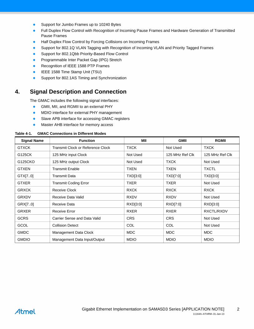
Support for Jumbo Frames up to 10240 BytesFull Duplex Flow Control with Recognition of Incoming Pause Frames and Hardware Generation of Transmitted Pause FramesHalf Duplex Flow Control by Forcing Collisions on Incoming FramesSupport for 802.1Q VLAN Tagging with Recognition of Incoming VLAN and Priority Tagged FramesSupport for 802.1Qbb Priority-Based Flow ControlProgrammable Inter Packet Gap (IPG) Stretch Recognition of IEEE 1588 PTP FramesIEEE 1588 Time Stamp Unit (TSU)Support for 802.1AS Timing and Synchronization
4. Signal Description and ConnectionThe GMAC includes the following signal interfaces:
GMII, MII, and RGMII to an external PHYMDIO interface for external PHY managementSlave APB interface for accessing GMAC registersMaster AHB interface for memory access
Table 4-1. GMAC Connections in Different Modes
Signal Name Function MII GMII RGMII
GTXCK Transmit Clock or Reference Clock TXCK Not Used TXCK
G125CK 125 MHz input Clock Not Used 125 MHz Ref Clk 125 MHz Ref Clk
G125CKO 125 MHz output Clock Not Used TXCK Not Used
GTXEN Transmit Enable TXEN TXEN TXCTL
GTX[7..0] Transmit Data TXD[3:0] TXD[7:0] TXD[3:0]
GTXER Transmit Coding Error TXER TXER Not Used
GRXCK Receive Clock RXCK RXCK RXCK
GRXDV Receive Data Valid RXDV RXDV Not Used
GRX[7..0] Receive Data RXD[3:0] RXD[7:0] RXD[3:0]
GRXER Receive Error RXER RXER RXCTL/RXDV
GCRS Carrier Sense and Data Valid CRS CRS Not Used
GCOL Collision Detect COL COL Not Used
GMDC Management Data Clock MDC MDC MDC
GMDIO Management Data Input/Output MDIO MDIO MDIO
2Gigabit Ethernet Implementation on SAMA5D3 Series [APPLICATION NOTE]11164A–ATARM–31-Jan-13

Figure 4-1. Connection between Ethernet PHY and Ethernet MAC in the MII/GMII Mode.
Figure 4-2. Connection between Ethernet PHY and Ethernet MAC in the RGMII Mode
3Gigabit Ethernet Implementation on SAMA5D3 Series [APPLICATION NOTE]11164A–ATARM–31-Jan-13

5. MII: Media Independent InterfaceThe MII bus (standardized by IEEE 802.3) is a generic bus that connects different types of PHYs to the same networkcontroller (MAC). The network controller may interact with any PHY using the same hardware interface, independent ofthe media the PHYs are connected to. The MII transfers data using 4bit words (nibble) in each direction, clocked at 25MHz to achieve 100 Mbit/s speed.
The basic operation of data transmission is that the enable signal (TXEN) is set active to indicate start of frame and untilit is completed. Then the clock signal (TXCLK) is set active for every group of bits (TXD[3:0]), at 2.5 MHz for 10 Mbit/smode and 25 MHz for 100 Mbit/s mode. When the reception is valid, the RXDV signal goes active when the frame startsand throughout the frame duration. Then the clock signal (RXCLK) goes active for every group of bits (RXD[3:0]). For theshortest possible frame this means ~130 clocks. Any frame transferred begins with sync bits before the data payload. Atpower-up, the PHY adapts to whatever it is connected to, unless you alter settings via the MDIO interface.
The following table describes MII signals:
Note: 1. Direction is defined from the chip side: IN = PHY to MAC, OUT = MAC to PHY.
Table 5-1. MII Signals
Channel Signal Direction(1) Description
PHY to MAC
TXCK IN Transmit clock (generated by the PHY): 2.5 MHz for 10 Mbit/s and 25 MHz for 100 Mbit/s
TXD[4:0] OUT Data to be transmitted
TXEN OUT Transmitter enable
TXER OUT Transmitter error (used to corrupt a packet)
MAC to PHY
RXCK IN Received clock
RXD[4:0] IN Received data
RXDV IN Signifies that received data is valid
RXER IN Signifies that received data has errors
Carrier and Collision
CRS IN Carrier Sense (half-duplex connections only)
COL IN Collision Detect (half-duplex connections only)
PHY Management
MDCK OUT
MDIO INOUT
4Gigabit Ethernet Implementation on SAMA5D3 Series [APPLICATION NOTE]11164A–ATARM–31-Jan-13

6. GMII: Gigabit Media Independent InterfaceGMII is an addendum to MII interface. It has been added to handle Gigabit Ethernet 1000 Mbit/s transfer rate. GMII doesnot replace MII, as it is not specified to work with 10 and 100 Mbit/s transfer rates. Therefore, for 10 or 100 Mbit/s transferrates, MII interface is used instead of GMII.
One of the major differences between MII and GMII is that TX clock (MAC to PHY clock) is not provided by the PHYanymore, it is the MAC that provides the clock. Then each of RX and TX channels provides its own clock. This preventstiming closure issues, as Gigabit mode frequency clock is 125 MHz (4 ns period). Four additional bits have been addedon Data signals in order to reach the 1000 Mbit/s rate (frequency is 5 times the one of 100 Mbit/s rate, and data bus widthis doubled, then the factor of 10 is reached).
The following table describes GMII signals:
Note: 1. Direction is defined from the chip side: IN = PHY to MAC, OUT = MAC to PHY.
Table 6-1. GMII Signals
Channel Signal Direction(1) Description
PHY to MAC
GTXCK OUT Transmit clock for 1000 Mbit/s: 125 MHz
TXCK INTransmit clock (generated by the PHY for MII compatibility): 2.5 MHz for 10 Mbit/s and 25 MHz for 100 Mbit/s
TXD[7:0] OUT Data to be transmitted (4 bits more than MII)
TXEN OUT Transmitter enable
TXER OUT Transmitter error (used to corrupt a packet)
MAC to PHY
RXCK IN Received clock
RXD[7:0] IN Received data (4 bits more than MII)
RXDV IN Signifies that received data is valid
RXER IN Signifies that received data has errors
Carrier and Collision
CRS IN Carrier Sense (half-duplex connections only)
COL IN Collision Detect (half-duplex connections only)
PHY Management
MDCK OUT SMI clock
MDIO INOUT SMI data
5Gigabit Ethernet Implementation on SAMA5D3 Series [APPLICATION NOTE]11164A–ATARM–31-Jan-13

7. RGMII: Reduced Gigabit Media Independent InterfaceRGMII uses half the number of data pins used in the GMII interface. This reduction is achieved by clocking data on boththe rising and the falling edges of the clock, and by eliminating non-essential signals (carrier sense and collisionindication).
Thus RGMII consists only of: RXC, RD[3:0], RX_CTL, TXC, TXD[3:0], and TX_CTL (12 pins, as opposed to 24 pins forGMII).
Unlike MII, the transmit clock signal is always provided by the MAC on the TXC line, rather than being provided by thePHY for 10/100 Mbit/s operation and by the MAC at 1000 Mbit/s.
RGMII supports Ethernet speeds of 10 Mbit/s, 100 Mbit/s and 1000 Mbit/s.
The following table describes RGMII signals:
Note: 1. Direction is defined from the chip side: IN = PHY to MAC, OUT = MAC to PHY.
Table 7-1. RGMII Signals
Channel Signal Direction(1) Description
Clock GTXCK IN 125 MHz reference clock
PHY to MAC
TX_CLK / GTXCKO OUT
Transmit clock (generated by the MAC with master clock GTXCK): 2.5 MHz for 10 Mbit/s, 25 MHz for 100 Mbit/s and 125 MHz for 1000 Mbit/s
TXD[3:0] OUT Data to be transmitted
TXCTL OUT Transmitter enable / Transmitter error
MAC to PHY
RXC IN Received clock: 2.5 MHz for 10 Mbit/s, 25 MHz for 100 Mbit/s and 125 MHz for 1000 Mbit/s
RXD[3:0] IN Received data
RXCTL IN Signifies that received data has errors
PHY Management
MDCK OUT SMI clock
MDIO INOUT SMI data
6Gigabit Ethernet Implementation on SAMA5D3 Series [APPLICATION NOTE]11164A–ATARM–31-Jan-13

8. Routing ConsiderationsThe user should refer to the design and layout guidelines of the PHY provider.
8.1 SAMA5D3 ExampleThis example shows how SAMA5D3-EK connects to KSZ9021GN PHY.
The functional mode is defined by the software. PHY is configured to operate in GMII, RGMII or MII mode, according tothe chosen hardware connection.
Figure 8-1. Functional Connection.
7Gigabit Ethernet Implementation on SAMA5D3 Series [APPLICATION NOTE]11164A–ATARM–31-Jan-13

Figure 8-2. Schematics Extract of SAMA5D3-EK
8Gigabit Ethernet Implementation on SAMA5D3 Series [APPLICATION NOTE]11164A–ATARM–31-Jan-13

Revision History
In the table that follows, the most recent version of the document appears first.
“rfo” indicates changes requested during the document review and approval loop.
Doc. Rev CommentsChange Request Ref.
11164A First issue.
9Gigabit Ethernet Implementation on SAMA5D3 Series [APPLICATION NOTE]11164A–ATARM–31-Jan-13

Atmel Corporation1600 Technology DriveSan Jose, CA 95110USATel: (+1) (408) 441-0311Fax: (+1) (408) 487-2600www.atmel.com
Atmel Asia LimitedUnit 01-5 & 16, 19FBEA Tower, Millennium City 5418 Kwun Tong RoadKwun Tong, KowloonHONG KONGTel: (+852) 2245-6100Fax: (+852) 2722-1369
Atmel Munich GmbHBusiness CampusParkring 4D-85748 Garching b. MunichGERMANYTel: (+49) 89-31970-0Fax: (+49) 89-3194621
Atmel Japan G.K.16F Shin-Osaki Kangyo Bldg1-6-4 Osaki, Shinagawa-kuTokyo 141-0032JAPANTel: (+81) (3) 6417-0300Fax: (+81) (3) 6417-0370
© 2013 Atmel Corporation. All rights reserved. / Rev.: 11164A–ATARM–31-Jan-13
Disclaimer: The information in this document is provided in connection with Atmel products. No license, express or implied, by estoppel or otherwise, to any intellectual property right is granted by thisdocument or in connection with the sale of Atmel products. EXCEPT AS SET FORTH IN THE ATMEL TERMS AND CONDITIONS OF SALES LOCATED ON THE ATMEL WEBSITE, ATMEL ASSUMESNO LIABILITY WHATSOEVER AND DISCLAIMS ANY EXPRESS, IMPLIED OR STATUTORY WARRANTY RELATING TO ITS PRODUCTS INCLUDING, BUT NOT LIMITED TO, THE IMPLIEDWARRANTY OF MERCHANTABILITY, FITNESS FOR A PARTICULAR PURPOSE, OR NON-INFRINGEMENT. IN NO EVENT SHALL ATMEL BE LIABLE FOR ANY DIRECT, INDIRECT,CONSEQUENTIAL, PUNITIVE, SPECIAL OR INCIDENTAL DAMAGES (INCLUDING, WITHOUT LIMITATION, DAMAGES FOR LOSS AND PROFITS, BUSINESS INTERRUPTION, OR LOSS OFINFORMATION) ARISING OUT OF THE USE OR INABILITY TO USE THIS DOCUMENT, EVEN IF ATMEL HAS BEEN ADVISED OF THE POSSIBILITY OF SUCH DAMAGES. Atmel makes norepresentations or warranties with respect to the accuracy or completeness of the contents of this document and reserves the right to make changes to specifications and products descriptions at any timewithout notice. Atmel does not make any commitment to update the information contained herein. Unless specifically provided otherwise, Atmel products are not suitable for, and shall not be used in,automotive applications. Atmel products are not intended, authorized, or warranted for use as components in applications intended to support or sustain life.
Atmel®, Atmel logo and combinations thereof, Enabling Unlimited Possibilities®, and others are registered trademarks or trademarks of Atmel Corporation or its subsidiaries. ARM®, ARMPowered® logo, Cortex™ are registered trademarks or trademarks of ARM Ltd.Other terms and product names may be trademarks of others.