atmel led driver-msl3162 - microchip...
TRANSCRIPT

Atmel LED Driver-MSL3162 16-string, RGB and White LED Drivers with AdaptivePower Control and 1MHz I2C/SMBus Serial Interface
Datasheet Brief

2 Atmel LED Driver-MSL3162
General Description
Atmel LED Driver-MSL3162
is a compact, high-power,
16-parallel-string LED driver.
It uses internal current control
MOSFETs to sink up to
100mA per LED string with
better than 3% accuracy and
with up to 10 series white
LEDs per string, or 160 LEDs
per MSL3162.
Atmel LED Driver-MSL316216-string, RGB and White LED Drivers with Adaptive Power Control and 1MHz I2C/SMBus Serial Interface
The advanced PWM engine is easily synchronized to the video signal and refresh timing using a built-in DLL multiplier and sync dividers. Per-string phase adjustment reduces unwanted LCD artifacts such as motion blur. Up to 16 MSL3162s can share the same 1MHz I2C/SMBus-compatible serial interface, which is fast enough for frame-by-frame LED string intensity control of 16 MSL3162s, or 2560 white LEDs in total.
The MSL3162 adaptively controls the voltage powering the LED strings using patented Atmel's Efficiency Optimizer control. The Efficiency Optimizer minimizes LED driver power losses while maintaining high current accuracy.
The MSL3162 uses 6-bit analog (LED current) dimming as well as 10-bit PWM dimming control. PWM dimming is derived from the product of the 8-bit individual string PWM setting, the 6-bit global intensity, and the 8-bit thermal derating. One external resistor provides the global reference current for all the LED strings.
The MSL3162 features fault monitoring of open circuit, short circuit, and over-temperature conditions, with fault status available through the dedicated FLTB output as well as the I2C/SMBus serial interface. It supports both individual device I2C read/write and broadcast write commands, allowing multiple MSL3162s to be configured simultaneously.
The MSL3162 includes on-chip user EEPROM, allowing customization of the internal register power-up defaults.
The MSL3162 is offered in a lead-free, halogen-free, RoHS-compliant package with a -40°C to +85°C temperature range.
ApplicationsLong Life, Efficient LED Backlighting for:
• Televisions and Desktop Monitors
• Medical and Industrial Instrumentation
• Automotive Audio-visual Displays
Digital Signage
Solid-State Lighting
Ordering Information
PART DESCRIPTION PACKAGE
MSL3162BT 16-ch LED driver 40-pin, 6x6x0.75mm TQFN

3Atmel LED Driver-MSL3162
Atmel LED Driver-MSL3162Atmel LED Driver-MSL316216-string, RGB and White LED Drivers with Adaptive Power Control and 1MHz I2C/SMBus Serial Interface
16-string, RGB and White LED Drivers with Adaptive Power Control and 1MHz I2C/SMBus Serial Interface
Key Features
Application Circuit
• 100ma Maximum Peak LED String Current
• Adaptive Power Correction Optimizes LED Supplies
• Multiple MSL3162s Can Share String Supplies
• MSL3162s Automatically Negotiate The Lowest Supply Voltage That Maintains Regulation Across All MSL3162s
• Better Than ±3% Current Accuracy and Balance
• Single Resistor Sets Peak Current For All LED Strings
• Individual LED String Intensity (Peak Current And PWM)
• Individual LED String Phase Controls
• Global LED Intensity Control – I2C Or PWM Input Pin
• Programmable String Phase Delays Reduce Motion Blur
• Supports Adaptive, Real-Time 2D Area Dimming For Highest Dynamic Range LCD TVs and Monitors
• Flexible Video Frame (VSYNC) And Line (HSYNC) Synchronization With DLL Multiplier and Dividers
• Sync Loss Detectors Optionally Disable LED Strings
• Open Circuit and Short Circuit Fault Detection
• Individual Fault Detection Enables For Each String
• 1Mhz I2C/SMbus Interface with 16 Slave Addresses
• I2C/SMbus Broadcast Mode Simplifies Configuration
• User EEPROM Saves Power-On Default Settings
• Die Over-Temperature Cutoff Protection
• <1µa LED String Current Sink Off Leakage Current
• Automatic LED Current Temperature Compensation
• -40°C To +85°C Operating Temperature Range
• Lead-Free, Halogen-Free, RoHs-Compliant Package

4 Atmel LED Driver-MSL3162
Quick Start GuideThe MSL3162 is an LED string driver that drives, monitors, and dims up to 160 white LEDs (up to 10 series and up to 16 parallel) at high efficiency for LCD backlighting and signage applications. This section summarizes the capabilities of the MSL3162 for quick evaluation.
How Many LEDS and Drivers?
The MSL3162 drives 16 strings of series-connected LEDs. The maximum number of LEDs per string is limited to 10 white LEDs by the 40V maximum string voltage rating. More series LEDs can be driven if their forward voltage (V
F) is
lower. When an LED string is turned off, the voltage across the LEDs does not drop to zero. This allows more series LEDs to be driven, but eliminates the MSL3162's ability to sustain a shorted LED string.
Sixteen MSL3162s can share an I2C/SMBus serial interface, with both individual and broadcast (all MSL3162s on a bus) addressing. The high total LED drive capability of multiple bussed MSL3162s makes the driver suitable for LCD TV and monitor backlights as well as LED signage and general lighting. The LED drive capability is summarized in Table 1.
LED TYPE VF(MAX)LEDs IN STRING
PER MSL3162
16 X MSL3162s
LED POWER PER MSL3162
LED POWER 16 X MSL3162s
White, Green, Blue 3.6V 10 LEDs 160 LEDs 2560 LEDs 34W
(at 60mA string current)544W
(at 60mA string current)Red 2.4V 15 LEDs 240 LEDs 3840 LEDs
RGB - 10 LEDs 50 RGB LEDs 800 RGB LEDs 26W (at 60mA) 415W (at 60mA)
LEDS, Power Supplies (PSUs), and Efficiency Optimizers
The MSL3162 obtains high efficiency by adjusting up to three LED string power supplies to deliver the minimum necessary voltage to accurately drive all LED strings connected to each LED string supply via the three Efficiency Optimizers. Multiple MSL3162s sharing string supplies automatically negotiate the voltage among themselves using the FBI/FBO pins. No system intervention is needed after initial configuration. Use any appropriate LED string power supply topology, typically a DC-DC boost or buck converter with a controllable resistive feedback voltage divider.
The Efficiency Optimizer sets the LED voltage to maintain regulation on the highest voltage LED string. The better the LED string voltage matching, the lower the dissipation the MSL3162 absorbs, and, therefore, better LED matching improves efficiency. RGB LEDs should be driven by three separate string supplies. Also, consider using multiple string supplies for high-power, single-color systems, such as a white backlight.
Table 1. Atmel LED Driver MSL3162 LED Drive Capability

5Atmel LED Driver-MSL3162
Timing, PWM, Intensity Controls and Synchronization
The internal PWM dimming is synchronized to the LCD's frame timing through the PHI input (typically VSYNC) and the GSC input (typically HSYNC) to eliminate beating artifacts and maintain high timing accuracy. Suitability for LED backlight architectures is shown in Table 2. LED area dimming for direct backlighting is supported for contrast improvement. Motion blur is reduced by setting each LED string's PWM phasing individually to synchronize PWM off times with the LCD refresh timing for the zone being lit.
BACKLIGHT TYPE STRING SUPPLY OPTIONS MOTION BLUR REMOVAL LED ZONE
MANAGEMENT
White LED – Bottom, edge-lit
Up to three efficiency optimized supplies
No No
White LED – Top/bottom, edge-lit No No
White LED – Four sides, edge-lit No No
White LED – Direct, back-lit Yes - LED strip phasing Higher contrast ratio (area dimming)
RGB LED – Direct, back-lit R, G, B efficiency optimized supplies Yes - LED strip phasing Higher contrast ratio and color
gamut
Table 2. Atmel LED Driver-MSL3162 LED Common Backlight Drive Architectures
Atmel LED Driver-MSL316216-string, RGB and White LED Drivers with Adaptive Power Control and 1MHz I2C/SMBus Serial Interface

6 Atmel LED Driver-MSL3162
Package Pin-out
Figure 1. 40-pin, 6mm x 6mm x 0.75mm TQFN (0.5mm pin pitch) with Exposed Pad
FBO
2 FB
I2
FBO
1 FB
I1
VD
D
VIN
E
N
ILE
D
N/C
G
ND
40 39 38 37 36 35 34 33 32 31
FBI3 1 30 N/C
FBO3 2 29 AD0
CGND 3 28 SDA
PHI 4 27 SCL
GSC 5 26 AD1
PWM 6 25 FLTB
STR0 7 24 STR15
STR1 8 23 STR14
STR2 9 22 STR13
STR3 10
MSL3162-TB
(TOP VIEW)
21 STR12 11 12 13 14 15 16 17 18 19 20
S
TR4
STR
5 S
TR6
STR
7 G
ND
C
GN
D
STR
8 S
TR9
STR
10
STR
11

7Atmel LED Driver-MSL3162
Package Pin-out
Figure 2. 40-pin TQFN Package Dimensions
Atmel LED Driver-MSL316216-string, RGB and White LED Drivers with Adaptive Power Control and 1MHz I2C/SMBus Serial Interface

8 Atmel LED Driver-MSL3162
Pin Descriptions
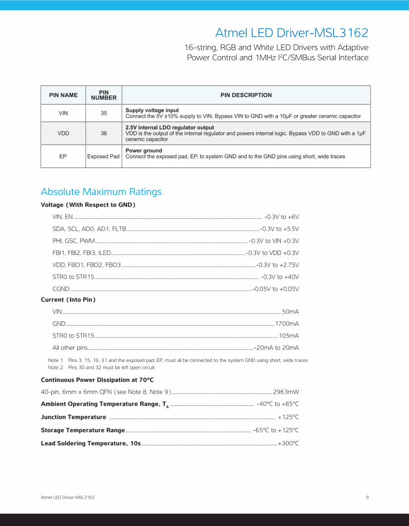
PIN NAME PIN NUMBER PIN DESCRIPTION
FBI1, FBI2, FBI3 37, 39, 1
Efficiency Optimizer feedback inputsWhen using a common LED voltage over multiple MSL3162s, connect FBIs and FBOs in a chain, with the first FBI grounded and the last FBO controlling the external power source. For standalone operation, connect FBI to GND.
FBO1, FBO2, FBO3 38, 40, 2
Efficiency Optimizer feedback outputsFBO controls the external regulator to dynamically adjust the LED voltage for optimal efficiency. When using a common LED voltage over multiple MSL3162s, connect FBIs and FBOs in a chain, with the first FBI grounded and the last FBO driving the feedback node of an external power source.
CGND 3, 16Signal groundConnect all CGND and GND pins to system GND and to the exposed pad, EP, using short, wide traces as close to the MSL3162 as possible
GND 15, 31Power groundConnect all GND and CGND pins to system GND and to the exposed pad, EP, using short, wide traces as close to the MSL3162 as possible
PHI 4Phase synchronization inputDrive PHI with an external signal from 40Hz to 10kHz to synchronize the MSL3162 PWM dimming to the signal at PHI. Connect PHI to GND if unused.
GSC 5Gate shift clock inputGSC sets the PWM dimming resolution. Drive GSC with the video signal gate shift clock up to 5MHz. Connect GSC to GND if unused.
PWM 6PWM dimming inputDrive PWM with a pulse-width modulated signal with a duty ratio ranging from 0% to 100% and frequency from 20Hz to 50kHz to control the brightness of all LED strings.
STR0to
STR15
7 - 14,17 - 24
STR0 to STR15 LED string current sink outputsConnect the cathode end of each series LED string to one of STR0 to STR15. Connect unused outputs to GND, and disable unused strings using the master control registers.
FLTB 25Fault indication output (open drain, active low)FLTB sinks current to GND whenever the MSL3162 detects a fault. Once a fault is detected, FLTB remains low until the fault registers have been read.
AD1, AD0 26, 29I²C slave ID selection inputsAD0 and AD1 select the I²C slave address used. Connect AD0 and AD1 to either GND, VDD, SCL, or SDA to select the slave ID.
SCL 27 I²C serial clock inputSCL is the I²C serial interface clock input.
SDA 28 I²C serial data I/OSDA is the I²C serial interface data I/O
N/C 30, 32 Factory connection. Leave unconnected.
ILED 33Maximum LED current control inputConnect a resistor from ILED to GND to set the full-scale LED string current. A 34.8kΩ resistor to GND sets a 60mA sink current through each LED string.
EN 34Enable input (active high)Drive EN high to turn on the MSL3162, and drive it low to turn it off. For automatic start-up, connect EN to VIN.
Table 3. Pin Descriptions
9Atmel LED Driver-MSL3162
Absolute Maximum RatingsVoltage (With Respect to GND)
VIN, EN .................................................................................................................................................................................... -0.3V to +6V
SDA, SCL, AD0, AD1, FLTB ...............................................................................................................................-0.3V to +5.5V
PHI, GSC, PWM .................................................................................................................................................. -0.3V to VIN +0.3V
FBI1, FBI2, FBI3, ILED ................................................................................................................................ -0.3V to VDD +0.3V
VDD, FBO1, FBO2, FBO3 ................................................................................................................................-0.3V to +2.75V
STR0 to STR15 ............................................................................................................................................................. -0.3V to +40V
CGND ..............................................................................................................................................................................-0.05V to +0.05V
Current (Into Pin)
VIN ..................................................................................................................................................................................................................50mA
GND .......................................................................................................................................................................................................1700mA
STR0 to STR15 ................................................................................................................................................................................105mA
All other pins ..............................................................................................................................................................-20mA to 20mA
Continuous Power Dissipation at 70°C
40-pin, 6mm x 6mm QFN (see Note 8, Note 9) ................................................................................................ 2963mW
Ambient Operating Temperature Range, TA ................................................................................. -40°C to +85°C
Junction Temperature ............................................................................................................................................................... +125°C
Storage Temperature Range ........................................................................................................................ -65°C to +125°C
Lead Soldering Temperature, 10s ..................................................................................................................................+300°C
Note 1. Pins 3, 15, 16, 31 and the exposed pad, EP, must all be connected to the system GND using short, wide tracesNote 2. Pins 30 and 32 must be left open circuit
PIN NAME PIN NUMBER PIN DESCRIPTION
VIN 35 Supply voltage inputConnect the 5V ±10% supply to VIN. Bypass VIN to GND with a 10µF or greater ceramic capacitor
VDD 362.5V internal LDO regulator outputVDD is the output of the internal regulator and powers internal logic. Bypass VDD to GND with a 1µF ceramic capacitor
EP Exposed PadPower ground Connect the exposed pad, EP, to system GND and to the GND pins using short, wide traces
Atmel LED Driver-MSL316216-string, RGB and White LED Drivers with Adaptive Power Control and 1MHz I2C/SMBus Serial Interface

10 Atmel LED Driver-MSL3162
Electrical Characteristics(Circuit of Figure 4, V
VIN = 5V, V
EN = 5V, default register settings of Table 5, T
A = -40°C to +85°C, unless otherwise noted. Typical values are at T
A = +25°C)
PARAMETER CONDITIONS AND NOTES MIN TYP MAX UNIT
DC ELECTRICAL CHARACTERISTICS
VIN operating supply voltage 4.5 5 5.5 V
VIN operating supply current Run mode; all LED strings driven 7 20 mA
VIN shutdown supply current Sleep mode; SDA, SCL, AD0, AD1, PWM, PHI, GSC at GND or VDD 20 25 µA
VDD regulation voltage 2.35 2.5 2.65 V
Input high voltageSDA, SCL, AD0, AD1, PWM, PHI, GSC
0.7 x VDD V
Input low voltageSDA, SCL, AD0, AD1, PWM, PHI, GSC
0.3 x VDD V
Input high voltage EN 1.2 V
Input low voltage EN 0.8 V
Output low voltage SDA Sinking 6mA 0.4 V
Output low voltage FLTB Sinking 6mA 0.6 V
ILED regulation voltage IILED = 10µA 340 355 370 mV
FBI_ feedback input current 0 140 μA
FBO_ feedback output current VFBO_ = 0 to 1.8V 0 55 μA
FBO_ feedback output current step size FBI_ = GND; TA = +25°C 2.5 3 3.6 μA
FBI_ input disable threshold (Note 10) 140 mV
LED string sink current STR0 to STR15
RILED = 34.8kΩ ±0.1%; ISTRn = 0x20; VSTRn = 1V;TA = +25°C
28.5 30 31.5 mA
58.9 mARILED = 34.8kΩ ±0.1%; ISTRn = 0x3F; VSTRn = 1V;TA = +25°C (Note 10)
LED string sink current matchingSTR0 to STR15 RILED = 34.8kΩ ±0.1%; ISTRn = 0x20; VSTRn = 1V; 3 %
LED string sink current maximumSTR0 to STR15 RILED = 20.5kΩ; ISTRn = 0x3F (Note 8, Note 9, Note 10) 100 mA
Short circuit fault detection threshold TA = +25°C 2.5 3.5 4.5 V
Thermal cutoff temperature (Note 10) 135 °C
Input leakage 10 µA
PARAMETER CONDITIONS AND NOTES MIN TYP MAX UNIT
AC ELECTRICAL CHARACTERISTICS
OSC initial accuracy OSCTRL = 0x04 (fOSC=20MHz); TA=25°C 18 20 22 MHz
PHI frequency 40 10000 Hz

11Atmel LED Driver-MSL3162
PARAMETER SYMBOL CONDITIONS AND NOTES MIN TYP MAX UNIT
I²C SWITCHING CHARACTERISTICS
SCL clock frequency 1/tSCL Bus timeout disabled (Note 2) 0 1000 kHz
Bus timeout period tTIMEOUT
OSCTRL = 0x04 (fOSC=20MHz); TA=25°C 27 30 33ms
OSCTRL = 0x00 to 0x07; fOSC=16 to 23MHz 600000 / fOSC
STOP to START condition bus free time tBUF 0.5 µs
Repeated START condition hold time tHD:STA 0.26 µs
Repeated START condition setup time tSU:STA 0.26 µs
STOP condition setup time tSU:STOP 0.26 µs
SDA data hold time tHD:DAT 5 ns
SDA data valid acknowledge time tVD:ACK (Note 3) 0.05 0.55 µs
SDA data valid time tVD:DAT (Note 4) 0.05 0.55 µs
SDA data set-up time tSU:DAT 100 ns
SCL clock low period tLOW 0.5 µs
SCL clock high period tHIGH 0.26 µs
SDA, SCL fall time tF (Note 5, Note 6) 120 ns
SDA, SCL rise time tR 120 ns
SDA, SCL input suppression filter period tSP (Note 7, Note 10) 50 ns
Note 1. All parameters are tested at TA=25°C unless otherwise noted. Specifications at temperature are guaranteed by design
Note 2. Minimum SCL clock frequency is limited by the bus timeout feature, which resets the serial bus interface if either SDA or SCL is held low for t
TIMEOUT. Disable bus timeout feature for DC operation
Note 3. tVD:ACK
= SCL low to SDA (out) low acknowledge timeNote 4. t
VD:DAT = minimum SDA output data-valid time following SCL low transition
Note 5. A master device must internally provide an SDA hold time of at least 300ns to ensure an SCL low stateNote 6. The maximum SDA and SCL rise times are 300ns. The maximum SDA fall time is 250ns. This allows series protection resistors to be
connected between SDA and SCL inputs and the SDA/SCL bus lines without exceeding the maximum allowable rise timeNote 7. MSL3162 includes input filters on SDA, SCL, AD0, and AD1 inputs that suppress noise less than 50nsNote 8. Subject to thermal dissipation characteristics of the deviceNote 9. When mounted according to JEDEC, JEP149, and JESD51-12 for a two-layer PCB, θ
JA = 18.6°C/W and θ
JC = 1.4°C/W
Note 10. Guaranteed by design and characterization. Not production tested
PARAMETER CONDITIONS AND NOTES MIN TYP MAX UNIT
GSC frequency 0 5 MHz
High and low time PHI, GSC 40 ns
PWM frequency 20 50000 Hz
PWM duty cycle 0.5 100 %
PHI DLL lock cycles (Note 10) 4 PHI cycles
Atmel LED Driver-MSL316216-string, RGB and White LED Drivers with Adaptive Power Control and 1MHz I2C/SMBus Serial Interface

12 Atmel LED Driver-MSL3162
Block Diagram
Figure 3. Atmel LED Driver-MSL3162 Block Diagram

13Atmel LED Driver-MSL3162
Typical Application Circuit
Figure 4. Single Atmel LED Driver-MSL3162 Driving 60 Red, 60 Green, and 60 Blue LED Strings at 60mA Per String
C1
1F
C2
1F
SDA
SCL
FLTB
PWM
HSY
NC
VSY
NC
EN
AB
LE
Rto
pBR
topG
Rto
pR
Rbo
ttom
RR
botto
mB
Rbo
ttom
G
VOU
TVO
UT
VOU
T
FBFB
FB
.
AD
126
AD
029
SDA
28SC
L27
FLTB
25
CG
ND
3
VIN35
VDD36
EN34
N/C
30
N/C32
PHI
4G
SC5
GND31
PWM
6ST
R0
7ST
R1
8ST
R2
9ST
R3
10
STR4 11STR5 12STR6 13STR7 14
STR8 17STR9 18STR10 19STR11 20
STR
1221
STR
1322
STR
1423
STR
1524
GND 15CGND 16
ILED33
EP
FBI137
FBO138
FBI239
FBO240
FBI3
1FB
O3
2
MSL
3162
BT
GN
D
GN
D
GN
D
GN
D
GN
D
GN
D
GN
D
GN
D
GN
D
GN
D
VD
D+5
V
Gre
en
LE
D S
trin
g
DC
-DC
Con
vert
er
Blu
eL
ED
Str
ing
DC
-DC
Con
vert
er
Red
LE
D S
trin
gD
C-D
CC
onve
rte
r
.
35k
RIL
ED
D2
CM
PSH
-3D
3C
MPS
H-3
D1
CM
PSH
-3
Atmel LED Driver-MSL316216-string, RGB and White LED Drivers with Adaptive Power Control and 1MHz I2C/SMBus Serial Interface

14 Atmel LED Driver-MSL3162
Detailed DescriptionInternal Regulators and Enable Input
Built-in current control MOSFETs capable of withstanding up to 40V provide a compact solution. The Efficiency Optimizer circuit controls the LED voltage generated by an external DC-DC converter to minimize losses on the current control MOSFETs, improving efficiency and reducing driver power dissipation. The MSL3162 uses a high-speed, 1MHz I2C serial interface to control LED current, PWM dimming, and fault detection circuitry, making it an optimal solution for driving LED backlights for LCD panels. Onboard EEPROM allows default settings to be reconfigured for customization and settings to be saved at turn-off, eliminating the need to re-write settings at the next turn-on. The tiny, 6mm x 6mm QFN package enables a compact solution while maintaining high power dissipation.
Internal Regulators and Enable Input
The MSL3162 includes an internal linear regulator that provides 2.5V supply voltage to power internal circuitry. Bypass VDD to GND with a 1µF or greater capacitor as close to the MSL3162 as possible.
The EN input turns the MSL3162 on and off. To turn on the MSL3162, drive EN high with a 5V logic level, and drive EN low to turn it off. When EN is low, the MSL3162 enters low-power mode, reducing input current to 20µA, and turns off the serial interface. For automatic start-up, connect EN to VIN, allowing the MSL3162 to start automatically when voltage is applied.
LED String Current Control
Each MSL3162 includes 16 current sink outputs, rated at 40V, each capable of sinking up to 100mA through a string of series connected LEDs. The internal Efficiency Optimizer circuit controls the LED voltage, minimizing power dissipated in the current sinks while maintaining high current-regulation accuracy. The MSL3162 power dissipation is limited to 2.1W. When using all 16 current sinks, maintain the total power dissipation within power dissipation limits.
Setting the Maximum LED String Current
The maximum IILED
current for the 16 LED strings STR0 to STR15 is set by external resistor R
ILED from the ILED
pin to GND and is determined by the equation:
ILEDILED R
I2050
=
where IILED
is in mA and RILED
is in kΩ.
RILED
=34.8kΩ sets the full-scale LED current to 58.9mA. R
ILED=20.5kΩ sets the full-scale LED current to 100mA,
the maximum allowed. The currents for the 16 LED strings, STR0 to STR15, are reduced individually from full scale with 6-bit resolution using the LED string current control registers.
If IILED
for the 16 LED strings, STR0 to STR15, is chosen to be 30mA or lower (by selecting the value of external resistor R
ILED to be greater than 68.3kΩ), then the
values programmed into the LED string current control registers must be limited to the range 0x00 to 0x1F. The full range of 0x00 to 0x3F is only available if I
ILED is
set to be greater than 30mA by using an RILED
value of 68.3kΩ or lower.

15Atmel LED Driver-MSL3162
Efficiency Optimizer
The Efficiency Optimizer improves power efficiency by adjusting each external LED power supply output voltage to the minimum required by the connected LED strings. It does this by injecting a current from the FBO output into the external LED power source voltage divider (Figure 5), thus lowering the LED supply voltage. The power supply's feedback voltage (internal reference voltage) must be 1.4V or less, and the voltage setting feedback network divider must be accessible. Use a Schottky diode (CMPSH-3 or similar) as shown to protect the power source against reverse current flow into the FBO pin, should the power supply circuit be powered before the MSL3162.
Figure 5. Atmel LED Driver-MSL3162FBO_Connection to Power Supply Voltage Divider
Connecting an LED String Power Supply to an Efficiency Optimizer
An LED string power supply uses a voltage divider (RTOP
and RBOTTOM
in Figure 6) to set its output voltage. The maximum output voltage is set by the voltage divider ratio and the power supply feedback regulation voltage per the equation:
BOTTOMTOP
BOTTOMMAXOUTFB RR
RVV+
= *)( or BOTTOM
BOTTOMTOPFBMAXOUT R
RRVV += *)(
VOUT(MAX)
must exceed the maximum LED string voltage to ensure regulation, but ensure that VOUT(MAX)
is always under the 40V maximum rating of the MSL3162’s LED string outputs, STR0 to STR15.
The Efficiency Optimizer modifies the feedback network by injecting a current, IFBO
, in the range of 0 to 45µA from the FBO output into the measurement node, FB. The minimum power supply output voltage is determined by the equation:
( )TOPMAXBOxFMAXOUTMINOUT RIVV *)()()( −=
where IFBOx(MAX)
is the 45µA maximum output current from the Efficiency Optimizer output.
From these equations, the equations to calculate the feedback resistors are:
)(
*MAXFBO
MINMAXFBTOP I
VVVR
−=
and
FBOUT
FBTOPBOTTOM VV
VRR−
= *
Atmel LED Driver-MSL316216-string, RGB and White LED Drivers with Adaptive Power Control and 1MHz I2C/SMBus Serial Interface

16 Atmel LED Driver-MSL3162
Using Multiple Atmel LED Driver-MSL3162s to Control a Single Power Supply
To use multiple MSL3162s to control a single power supply, connect the FBOx output of one MSL3162 to the FBIx input of another MSL3162 to form a chain(Figure 6). The Efficiency Optimizer decides whether the current at the FBIx input is less than what the FBOx output is programmed to. If the FBIx current is less than the programmed current, the FBIx current is transferred to the FBOx output. Otherwise, the programmed current is used at FBOx. The power supply output is, therefore, programmed to the minimum voltage required by all MSL3162s controlling it, and so all LED strings have sufficient voltage to maintain current regulation and power supply noise rejection.
Figure 6. Cascade Multiple Atmel LED Driver-MSL3162s to Control a Common Power Supply
The accuracy of the FBOx output current can degrade through each link of the FBIx/FBOx chain by as much as 2%. Therefore, the maximum output voltage correction current can drop by 2% per link. Calculate the worst-case FBOx current by the equation:
( ) 1)/( 98.0*45 −= N
MINMAXFBOx µAI
where IFBOx(MAX/MIN)
is the worst-case (minimum) maximum FBOx output current, and N is the number of MSL3162 FBIx/FBOx I/Os connected in series.
Take care in laying out the traces for the Efficiency Optimizer FBIx/FBOx I/Os. If the FBIx input is not used, connect it to GND as close to the MSL3162 as possible. When routing the FBIx/FBOx signals across circuit boards, minimize the trace length as much as possible. Do not route the traces close to other traces with large variations in voltage or current because such traces may couple noise into the FBIx/FBOx I/Os. If these traces must be routed near noisy signals, shield them from noise by use of ground planes or guard traces.
17Atmel LED Driver-MSL3162
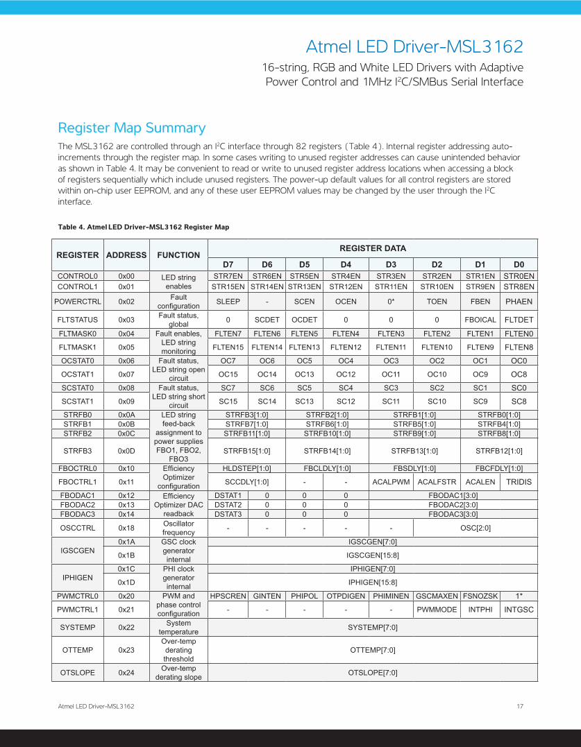
Register Map SummaryThe MSL3162 are controlled through an I2C interface through 82 registers (Table 4). Internal register addressing auto-increments through the register map. In some cases writing to unused register addresses can cause unintended behavior as shown in Table 4. It may be convenient to read or write to unused register address locations when accessing a block of registers sequentially which include unused registers. The power-up default values for all control registers are stored within on-chip user EEPROM, and any of these user EEPROM values may be changed by the user through the I2C interface.
Table 4. Atmel LED Driver-MSL3162 Register Map
REGISTER ADDRESS FUNCTIONREGISTER DATA
D7 D6 D5 D4 D3 D2 D1 D0CONTROL0 0x00 LED string
enablesSTR7EN STR6EN STR5EN STR4EN STR3EN STR2EN STR1EN STR0EN
CONTROL1 0x01 STR15EN STR14EN STR13EN STR12EN STR11EN STR10EN STR9EN STR8EN
POWERCTRL 0x02 Fault configuration SLEEP - SCEN OCEN 0* TOEN FBEN PHAEN
FLTSTATUS 0x03 Fault status, global 0 SCDET OCDET 0 0 0 FBOICAL FLTDET
FLTMASK0 0x04 Fault enables, LED string monitoring
FLTEN7 FLTEN6 FLTEN5 FLTEN4 FLTEN3 FLTEN2 FLTEN1 FLTEN0
FLTMASK1 0x05 FLTEN15 FLTEN14 FLTEN13 FLTEN12 FLTEN11 FLTEN10 FLTEN9 FLTEN8
OCSTAT0 0x06 Fault status, LED string open
circuit
OC7 OC6 OC5 OC4 OC3 OC2 OC1 OC0
OCSTAT1 0x07 OC15 OC14 OC13 OC12 OC11 OC10 OC9 OC8
SCSTAT0 0x08 Fault status, LED string short
circuit
SC7 SC6 SC5 SC4 SC3 SC2 SC1 SC0
SCSTAT1 0x09 SC15 SC14 SC13 SC12 SC11 SC10 SC9 SC8
STRFB0 0x0A LED string feed-back
assignment to power supplies FBO1, FBO2,
FBO3
STRFB3[1:0] STRFB2[1:0] STRFB1[1:0] STRFB0[1:0]STRFB1 0x0B STRFB7[1:0] STRFB6[1:0] STRFB5[1:0] STRFB4[1:0]STRFB2 0x0C STRFB11[1:0] STRFB10[1:0] STRFB9[1:0] STRFB8[1:0]
STRFB3 0x0D STRFB15[1:0] STRFB14[1:0] STRFB13[1:0] STRFB12[1:0]
FBOCTRL0 0x10 Efficiency Optimizer
configuration
HLDSTEP[1:0] FBCLDLY[1:0] FBSDLY[1:0] FBCFDLY[1:0]
FBOCTRL1 0x11 SCCDLY[1:0] - - ACALPWM ACALFSTR ACALEN TRIDIS
FBODAC1 0x12 Efficiency Optimizer DAC
readback
DSTAT1 0 0 0 FBODAC1[3:0]FBODAC2 0x13 DSTAT2 0 0 0 FBODAC2[3:0]FBODAC3 0x14 DSTAT3 0 0 0 FBODAC3[3:0]
OSCCTRL 0x18 Oscillator frequency - - - - - OSC[2:0]
IGSCGEN0x1A GSC clock
generator internal
IGSCGEN[7:0]
0x1B IGSCGEN[15:8]
IPHIGEN0x1C PHI clock
generator internal
IPHIGEN[7:0]
0x1D IPHIGEN[15:8]
PWMCTRL0 0x20 PWM and phase control configuration
HPSCREN GINTEN PHIPOL OTPDIGEN PHIMINEN GSCMAXEN FSNOZSK 1*
PWMCTRL1 0x21 - - - - - PWMMODE INTPHI INTGSC
SYSTEMP 0x22 System temperature SYSTEMP[7:0]
OTTEMP 0x23Over-temp derating threshold
OTTEMP[7:0]
OTSLOPE 0x24 Over-temp derating slope OTSLOPE[7:0]
Atmel LED Driver-MSL316216-string, RGB and White LED Drivers with Adaptive Power Control and 1MHz I2C/SMBus Serial Interface
18 Atmel LED Driver-MSL3162
REGISTER ADDRESS FUNCTIONREGISTER DATA
D7 D6 D5 D4 D3 D2 D1 D0
GSCMAX 0x25 Max osc. cycles per GSC pulse
GSCMAX[7:0]0x26 GSCMAX[15:8]
PHIMIN 0x27 Min GSC pulses over PHI period
PHIMIN[7:0]0x28 - - - - PHIMIN[15:8]
HPSCR 0x29 GSC divider - - - - HPSCR[3:0]
FRATE 0x2A PHI freq. multiplier - - - FRATE[4:0]
GINT 0x2B Global intensity - - GINT[6:0]ISTR0 0x30 LED string
6-bit individual analog current
settings
- - ISTR0[5:0]to - - to
ISTR15 0x3F - - ISTR15[5:0]
PHDLY0 0x40 LED string 8-bit individual PWMphase settings
PHDLY0[7:0]to to
PHDLY15 0x4F PHDLY15[7:0]PWM0 0x50 LED string 8-bit
individual PWM intensity settings
PWM0[7:0]to to
PWM15 0x5F PWM15[7:0]Do not access address range 0x60 to 0x8F
E2ADDR 0x90 User EEPROM read/write
access
- E2ADDR[6:0]
E2CTRLSTA 0x91 E2BUSY BLDACT E2ERR SLVATCNT[1:0] RWCTRL[1:0]
Table 4. Atmel LED Driver-MSL3162 Register Map
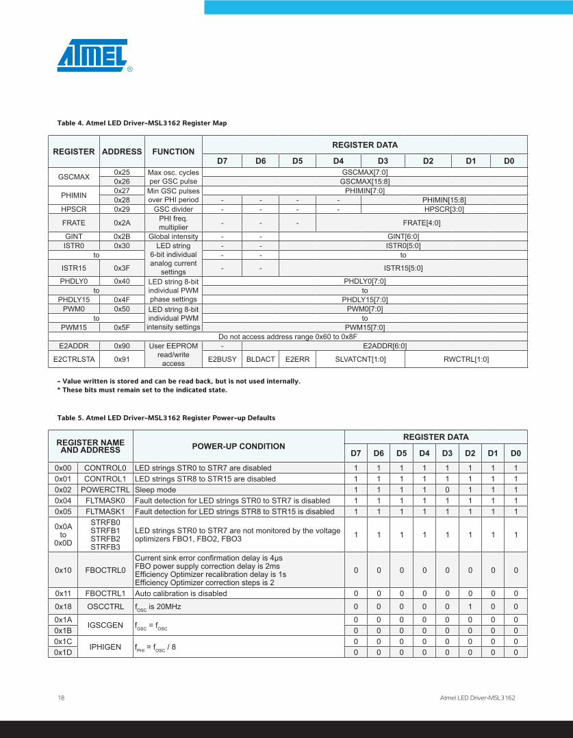
- Value written is stored and can be read back, but is not used internally.* These bits must remain set to the indicated state.
REGISTER NAMEAND ADDRESS POWER-UP CONDITION
REGISTER DATA
D7 D6 D5 D4 D3 D2 D1 D0
0x00 CONTROL0 LED strings STR0 to STR7 are disabled 1 1 1 1 1 1 1 10x01 CONTROL1 LED strings STR8 to STR15 are disabled 1 1 1 1 1 1 1 10x02 POWERCTRL Sleep mode 1 1 1 1 0 1 1 10x04 FLTMASK0 Fault detection for LED strings STR0 to STR7 is disabled 1 1 1 1 1 1 1 10x05 FLTMASK1 Fault detection for LED strings STR8 to STR15 is disabled 1 1 1 1 1 1 1 1
0x0Ato
0x0D
STRFB0STRFB1STRFB2STRFB3
LED strings STR0 to STR7 are not monitored by the voltage optimizers FBO1, FBO2, FBO3 1 1 1 1 1 1 1 1
0x10 FBOCTRL0Current sink error confirmation delay is 4µsFBO power supply correction delay is 2msEfficiency Optimizer recalibration delay is 1sEfficiency Optimizer correction steps is 2
0 0 0 0 0 0 0 0
0x11 FBOCTRL1 Auto calibration is disabled 0 0 0 0 0 0 0 0
0x18 OSCCTRL fOSC is 20MHz 0 0 0 0 0 1 0 0
0x1AIGSCGEN fGSC = fOSC
0 0 0 0 0 0 0 00x1B 0 0 0 0 0 0 0 00x1C
IPHIGEN fPHI = fOSC / 80 0 0 0 0 0 0 0
0x1D 0 0 0 0 0 0 0 0
Table 5. Atmel LED Driver-MSL3162 Register Power-up Defaults
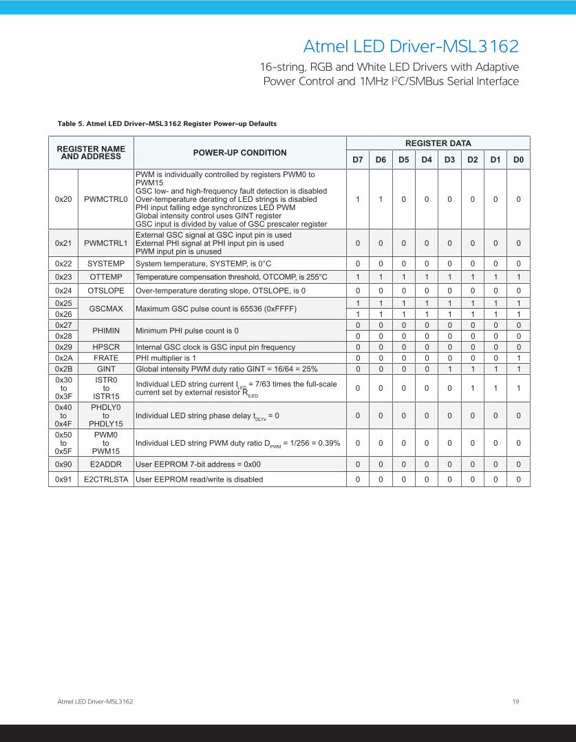
19Atmel LED Driver-MSL3162
Table 5. Atmel LED Driver-MSL3162 Register Power-up Defaults
REGISTER NAMEAND ADDRESS POWER-UP CONDITION
REGISTER DATA
D7 D6 D5 D4 D3 D2 D1 D0
0x20 PWMCTRL0
PWM is individually controlled by registers PWM0 to PWM15GSC low- and high-frequency fault detection is disabledOver-temperature derating of LED strings is disabledPHI input falling edge synchronizes LED PWMGlobal intensity control uses GINT registerGSC input is divided by value of GSC prescaler register
1 1 0 0 0 0 0 0
0x21 PWMCTRL1External GSC signal at GSC input pin is usedExternal PHI signal at PHI input pin is usedPWM input pin is unused
0 0 0 0 0 0 0 0
0x22 SYSTEMP System temperature, SYSTEMP, is 0°C 0 0 0 0 0 0 0 0
0x23 OTTEMP Temperature compensation threshold, OTCOMP, is 255°C 1 1 1 1 1 1 1 1
0x24 OTSLOPE Over-temperature derating slope, OTSLOPE, is 0 0 0 0 0 0 0 0 00x25
GSCMAX Maximum GSC pulse count is 65536 (0xFFFF)1 1 1 1 1 1 1 1
0x26 1 1 1 1 1 1 1 10x27
PHIMIN Minimum PHI pulse count is 00 0 0 0 0 0 0 0
0x28 0 0 0 0 0 0 0 00x29 HPSCR Internal GSC clock is GSC input pin frequency 0 0 0 0 0 0 0 00x2A FRATE PHI multiplier is 1 0 0 0 0 0 0 0 10x2B GINT Global intensity PWM duty ratio GINT = 16/64 = 25% 0 0 0 0 1 1 1 10x30
to0x3F
ISTR0to
ISTR15Individual LED string current ILED = 7/63 times the full-scale current set by external resistor RILED
0 0 0 0 0 1 1 1
0x40 to
0x4F
PHDLY0to
PHDLY15Individual LED string phase delay tDLYx = 0 0 0 0 0 0 0 0 0
0x50 to
0x5F
PWM0 to
PWM15Individual LED string PWM duty ratio DPWM = 1/256 = 0.39% 0 0 0 0 0 0 0 0
0x90 E2ADDR User EEPROM 7-bit address = 0x00 0 0 0 0 0 0 0 0
0x91 E2CTRLSTA User EEPROM read/write is disabled 0 0 0 0 0 0 0 0
Atmel LED Driver-MSL316216-string, RGB and White LED Drivers with Adaptive Power Control and 1MHz I2C/SMBus Serial Interface

Atmel Corporation2325 Orchard Parkway
San Jose, CA 95131
USA
Tel: (+1)(408) 441-0311
Fax: (+1)(408) 487-2600
www.atmel.com
© 2011 Atmel Corporation. All rights reserved. / Rev.: MSL3162DB1-E-US_06-11
Atmel®, logo and combinations thereof, and others are registered trademarks or trademarks of Atmel Corporation or its subsidiaries. Other terms and product names may be
trademarks of others.
Disclaimer: The information in this document is provided in connection with Atmel products. No license, express or implied, by estoppel or otherwise, to any intellectual property right is granted by this document or in connection with the sale of Atmel products. EXCEPT AS SET FORTH IN THE ATMEL TERMS AND CONDITIONS OF SALES LOCATED ON THE ATMEL WEBSITE, ATMEL ASSUMES NO LIABILITY WHATSOEVER AND DISCLAIMS ANY EXPRESS, IMPLIED OR STATUTORY WARRANTY RELATING TO ITS PRODUCTS INCLUDING, BUT NOT LIMITED TO, THE IMPLIED WARRANTY OF MERCHANTABILITY, FITNESS FOR A PARTICULAR PURPOSE, OR NON-INFRINGEMENT. IN NO EVENT SHALL ATMEL BE LIABLE FOR ANY DIRECT, INDIRECT, CONSEQUENTIAL, PUNITIVE, SPECIAL OR INCIDENTAL DAMAGES (INCLUDING, WITHOUT LIMITATION, DAMAGES FOR LOSS AND PROFITS, BUSINESS INTERRUPTION, OR LOSS OF INFORMATION) ARISING OUT OF THE USE OR INABILITY TO USE THIS DOCUMENT, EVEN IF ATMEL HAS BEEN ADVISED OF THE POSSIBILITY OF SUCH DAMAGES. Atmel makes no representations or warranties with respect to the accuracy or completeness of the contents of this document and reserves the right to make changes to specifications and products descriptions at any time without notice. Atmel does not make any commitment to update the information contained herein. Unless specifically provided otherwise, Atmel products are not suitable for, and shall not be used in, automotive applications. Atmel products are not intended, authorized, or warranted for use as components in applications intended to support or sustain life.
Atmel Asia LimitedUnit 01-5 & 16, 19F
BEA Tower, Millennium City 5
418 Kwun Tong Road
Kwun Tong, Kowloon
HONG KONG
Tel: (+852) 2245-6100
Fax: (+852) 2722-1369
Atmel Munich GmbHBusiness Campus
Parkring 4
D-85748 Garching b. Munich
GERMANY
Tel: (+49) 89-31970-0
Fax: (+49) 89-3194621
Atmel Japan9F, Tonetsu Shinkawa Bldg.
1-24-8 Shinkawa
Chuo-ku, Tokyo 104-0033
JAPAN
Tel: (+81)(3) 3523-3551
Fax: (+81)(3) 3523-7581