atom lithography of iron - pure - aanmelden
TRANSCRIPT

Atom lithography of iron
Citation for published version (APA):Sligte, te, E. (2005). Atom lithography of iron. Technische Universiteit Eindhoven.https://doi.org/10.6100/IR590725
DOI:10.6100/IR590725
Document status and date:Published: 01/01/2005
Document Version:Publisher’s PDF, also known as Version of Record (includes final page, issue and volume numbers)
Please check the document version of this publication:
• A submitted manuscript is the version of the article upon submission and before peer-review. There can beimportant differences between the submitted version and the official published version of record. Peopleinterested in the research are advised to contact the author for the final version of the publication, or visit theDOI to the publisher's website.• The final author version and the galley proof are versions of the publication after peer review.• The final published version features the final layout of the paper including the volume, issue and pagenumbers.Link to publication
General rightsCopyright and moral rights for the publications made accessible in the public portal are retained by the authors and/or other copyright ownersand it is a condition of accessing publications that users recognise and abide by the legal requirements associated with these rights.
• Users may download and print one copy of any publication from the public portal for the purpose of private study or research. • You may not further distribute the material or use it for any profit-making activity or commercial gain • You may freely distribute the URL identifying the publication in the public portal.
If the publication is distributed under the terms of Article 25fa of the Dutch Copyright Act, indicated by the “Taverne” license above, pleasefollow below link for the End User Agreement:www.tue.nl/taverne
Take down policyIf you believe that this document breaches copyright please contact us at:[email protected] details and we will investigate your claim.
Download date: 01. Dec. 2021
Atom Lithography
of Iron
PROEFSCHRIFT
ter verkrijging van de graad van doctor aan deTechnische Universiteit Eindhoven, op gezag vande Rector Magnificus, prof.dr.ir. C.J. van Duijn,voor een commissie aangewezen door het Collegevoor Promoties in het openbaar te verdedigen opmaandag 9 mei 2005 om 16.00 uur
door
Edwin te Sligte
geboren te Gouda
Dit proefschrift is goedgekeurd door de promotoren:
prof.dr. K.A.H. van Leeuwenenprof.dr. H.C.W. Beijerinck
Druk: Universiteitsdrukkerij Technische Universiteit EindhovenOntwerp omslag: Jan-Willem Luijten
CIP-DATA LIBRARY TECHNISCHE UNIVERSITEIT EINDHOVEN
Sligte, Edwin te
Atom Lithography of Iron / door Edwin te Sligte. -Eindhoven : Technische Universiteit Eindhoven, 2005 . - Proefschrift.ISBN 90-386-2201-5NUR 926Trefw.: atomaire bundels / deeltjesoptica / lithografie / nanotechnologie /magnetische dunne lagen / oppervlaktefysicaSubject headings: atomic beams / lithography / magnetic thin films / nan-otechnology / particle optics / surface physics
Contents
1 Introduction 3
1 Atom lithography . . . . . . . . . . . . . . . . . . . . . . . . . . . . . . . . . . 4
2 Laser cooling . . . . . . . . . . . . . . . . . . . . . . . . . . . . . . . . . . . . . 7
3 This thesis . . . . . . . . . . . . . . . . . . . . . . . . . . . . . . . . . . . . . . . 8
2 The choice for iron and its consequences 11
1 Choice of element . . . . . . . . . . . . . . . . . . . . . . . . . . . . . . . . . . 11
2 Fe source . . . . . . . . . . . . . . . . . . . . . . . . . . . . . . . . . . . . . . . . 13
3 Samples . . . . . . . . . . . . . . . . . . . . . . . . . . . . . . . . . . . . . . . . 17
4 Corrosion protection . . . . . . . . . . . . . . . . . . . . . . . . . . . . . . . . 17
5 Conclusions . . . . . . . . . . . . . . . . . . . . . . . . . . . . . . . . . . . . . . 18
3 Atoms in standing waves 21
1 Theory . . . . . . . . . . . . . . . . . . . . . . . . . . . . . . . . . . . . . . . . . 21
2 Numerical model . . . . . . . . . . . . . . . . . . . . . . . . . . . . . . . . . . . 25
3 Results . . . . . . . . . . . . . . . . . . . . . . . . . . . . . . . . . . . . . . . . . 28
4 Experimental apparatus 31
1 Vacuum system . . . . . . . . . . . . . . . . . . . . . . . . . . . . . . . . . . . 31
2 Fe source . . . . . . . . . . . . . . . . . . . . . . . . . . . . . . . . . . . . . . . . 33
3 Deposition . . . . . . . . . . . . . . . . . . . . . . . . . . . . . . . . . . . . . . . 36
4 Effusive Ag source . . . . . . . . . . . . . . . . . . . . . . . . . . . . . . . . . . 38
5 Optical system . . . . . . . . . . . . . . . . . . . . . . . . . . . . . . . . . . . . 39
6 Conclusion . . . . . . . . . . . . . . . . . . . . . . . . . . . . . . . . . . . . . . 44
5 Deposition experiments 47
1 Procedure . . . . . . . . . . . . . . . . . . . . . . . . . . . . . . . . . . . . . . . 47
2 Fe nanolines . . . . . . . . . . . . . . . . . . . . . . . . . . . . . . . . . . . . . . 48
3 Magnetism of thin films . . . . . . . . . . . . . . . . . . . . . . . . . . . . . . 52
6 Magnetism of periodic nanostructures 55
1 Demagnetizing field . . . . . . . . . . . . . . . . . . . . . . . . . . . . . . . . . 56
2 Energy of ferromagnetic nanostructures . . . . . . . . . . . . . . . . . . . . 57
3 Magnetic anisotropy model . . . . . . . . . . . . . . . . . . . . . . . . . . . . 59
1
CONTENTS
4 Calculated demagnetizing field . . . . . . . . . . . . . . . . . . . . . . . . . . 63
5 Calculated anisotropy field . . . . . . . . . . . . . . . . . . . . . . . . . . . . 66
6 Concluding remarks . . . . . . . . . . . . . . . . . . . . . . . . . . . . . . . . . 71
A Appendix . . . . . . . . . . . . . . . . . . . . . . . . . . . . . . . . . . . . . . . 74
7 Quantum Features in Atomic Nanofabrication using Exactly Resonant Stand-
ing Waves 77
8 Barrier-limited surface diffusion in atom lithography 85
1 Introduction . . . . . . . . . . . . . . . . . . . . . . . . . . . . . . . . . . . . . . 85
2 Numerical model . . . . . . . . . . . . . . . . . . . . . . . . . . . . . . . . . . . 87
3 Simulation parameters . . . . . . . . . . . . . . . . . . . . . . . . . . . . . . . 89
4 Pollutant limited surface diffusion . . . . . . . . . . . . . . . . . . . . . . . . 90
5 ES-barrier limited surface diffusion . . . . . . . . . . . . . . . . . . . . . . . 96
6 Conclusions . . . . . . . . . . . . . . . . . . . . . . . . . . . . . . . . . . . . . . 99
Summary 101
Samenvatting 102
Dankwoord 103
Curriculum Vitae 104
2
Chapter 1
Introduction
Optical lithography has enabled the microelectronics industry to achieve phenom-
enal growth and innovation rates over the past half century. The main cause for
this tremendous growth rate has been the relative ease with which the technique can
be applied to make ever smaller structures. At the turn of the 21st century, how-
ever, it has come close to some of its fundamental limits. The most noteworthy of
these limits is the size of the features that can be manufactured, a very important
characteristic in a field where smaller is often considered the definition of better.
In optical lithography, a pattern is most commonly transferred into a hard ma-
terial by coating it with a light-sensitive film - known as resist - and then selectively
illuminating the desired parts of the resist. This selective illumination is achieved by
placing a mechanical mask - called the reticle - in the light beam. The patterned light
beam is then projected on the sample. A selective chemical etchant then removes
either the unexposed or the exposed areas of the resist. The exposed underlying
material can then be removed in a plasma reactor, where the remaining areas of re-
sist act as an etch mask. After removing the remainder of the film, the patterned
layer remains. This technique can create arbitrary shapes, but with sizes limited
roughly to the wavelength of the light used to illuminate the mask film. The current
industry standard is 193 nm light; the attainable feature size is around 70 nm [1].
The industry road-map projects a shift to 14 nm extreme UV light in the next ten
years [2].
In atom lithography, on the other hand, light and matter change places. Now, a
spatial distribution of nearly-resonant light (called a light mask) modifies the profile
of a matter flux (in practice, an atomic beam). The atoms in the beam can then either
react with a suitable masking layer on a surface, developing it, or be deposited di-
rectly onto the surface. The first case directly parallels conventional lithography; the
latter, called direct write atom lithography, has no equivalent in optical lithography.
It is a simple, one-step nanostructuring process, in which the diffraction limit hardly
plays a role due to the small De Broglie wavelength of the atoms. Furthermore, the
process can be combined with the deposition of a second material, resulting in a
material with a structured doping on the nanoscale.
As optical lithography was used to create ever smaller ferromagnetic nanostruc-
tures, a fascinating physical properties came to light, such as quantized spin wave
3
INTRODUCTION
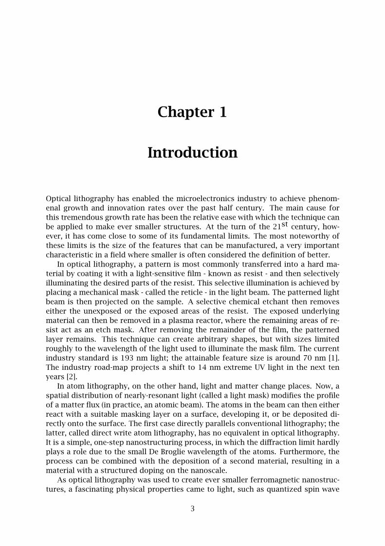
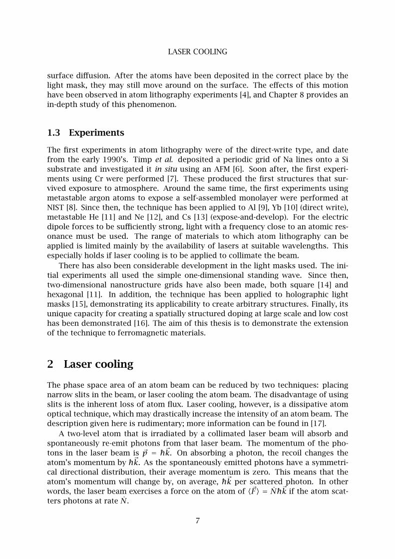
Figure 1.1: Principle of atom lithography. Atoms are focused by the induced dipole inter-
action with a standing wave. We intend to use this scheme to create arrays of 1D or 0D
ferromagnetic nanostructures.
spectra [3]. Atom lithography offers the possibility to create structures on the order
of 20 nm wide, with periods below 100 nm. Hence, the focus of this thesis is on the
application of direct write atom lithography to create ferromagnetic nanostructures.
1 Atom lithography
Atom lithography is usually practiced by focusing of atoms in the periodic potential
created by a standing laser light wave, as depicted in Fig. 1.1. Atoms exposed to a
light field experience a dipole force as a result of the electric field of the standing
wave. This results in a sinusoidal potential. The atoms are drawn towards the po-
tential minima; by placing a substrate in or behind the standing wave, one obtains
an array of nanolines. The following will be a simplified description of the principle
underlying the interaction of atoms and light masks. A more detailed description of
some of the physics of the atom-standing wave interaction will be given in Chapters 3
and 7.
1.1 Principle
The interaction of an atom with a light mask may in some cases be understood
classically. An electric field will induce a dipole moment in an atom. This dipole
moment will interact with the electric field it is in. The energy of this interaction is:
Udip = −~p · ~E, (1.1)
where ~p is the induced dipole moment and ~E is the applied field. For moderate
values of |~E|, the induced dipole moment is linear with respect to the applied field.
For an electric field that is caused by laser radiation, the potential may thus be
written in terms of the intensity I:
Udip = −α~E · ~E = −2α
ǫ0cI. (1.2)
4
ATOM LITHOGRAPHY
Usually, the polarizability α of the atoms is very small, and the effect is negligi-
ble. However, near an atomic resonance, its value increases by orders of magnitude.
Hence, we use nearly resonant laser light to control the atoms.
The simplest form of light mask conceivable is a one-dimensional standing wave.
In a Gaussian standing wave of beam radius w, the intensity profile I(~r) is given by:
I(~r) = 8P
πw2sin2(kx) exp
[
− 2(y2 + z2)
w2
]
. (1.3)
Here the wave propagates in the x direction with wave number k. The sign of the po-
tential is determined by the sign of the polarizability α. For an excitation frequency
below the resonance frequency, the induced dipole will be in phase with the field
and α > 0. This means that the atoms will be drawn towards the areas of maximum
intensity. Conversely, they will be pushed away from the intensity maxima for light
at higher frequencies than the atomic resonance.
For an exactly resonant light mask, the induced dipole moment will be phase
shifted by π/2 with respect to the electric field. Hence, its interaction energy with
the field will be zero. At this point, the classical description fails; quantum mechan-
ics predicts a rich interaction. The atom flux distribution is affected by all properties
of the standing wave. Chapter 7 presents an in-depth study of these phenomena.
1.2 Aberrations
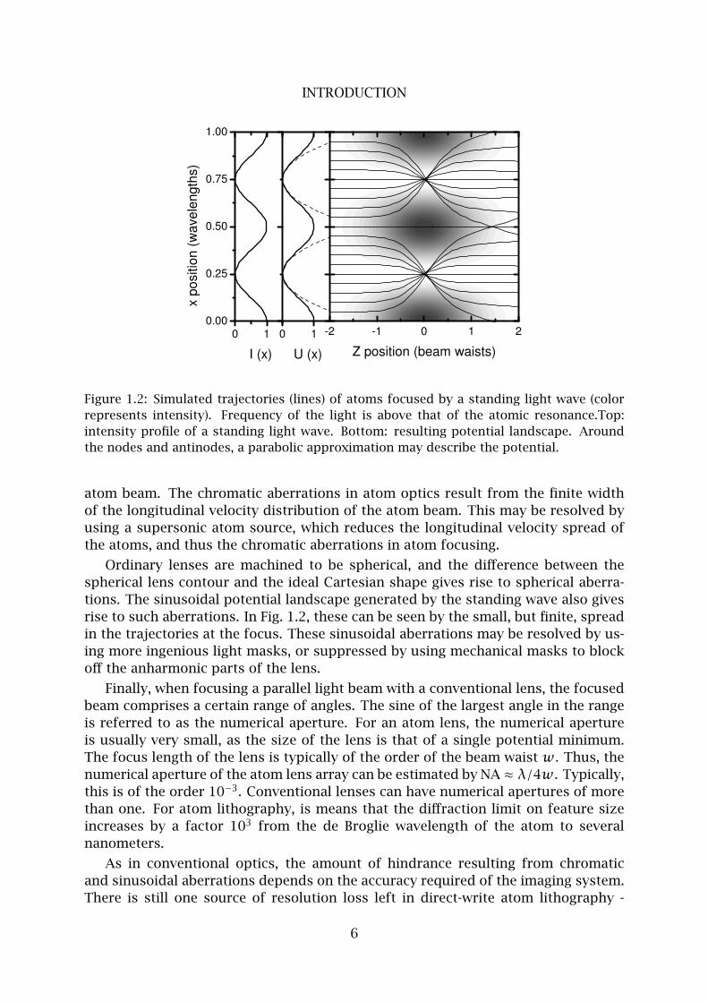
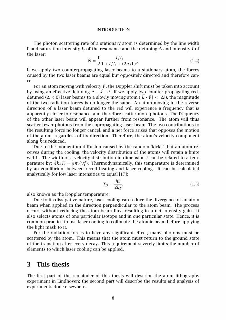
Figure 1.2 displays the intensity profile of a standing wave (left) and the resulting
potential landscape (center) for the case of positive detuning. Around the potential
minima, a parabolic approximation can be made (shown in the Figure as the dashed
line). In this region, the potential is that of a harmonic oscillator, in which the period
of an oscillation is independent of its amplitude. Atoms that start in a stationary
state will all converge on the potential minimum after a quarter oscillation time.
This focusing effect means that the standing wave acts as an infinite array of lenses.
The interaction of an atom beam with this lens array can be considered very similarly
to the classical focusing of a light beam using a normal lens array. An even more
accurate analogy in classical optics is an array of Gradient Index (GrIn) lenses.
The errors in the focusing can also be considered similarly to classical optical
aberrations. Foremost, the size of a projected image scales linearly with the size
of the original [5]. In atom optical terms, the largest contribution to the feature
size results from the finite (x,px) phase space area of the atom beam source. Laser
cooling is commonly used to reduce this error by non-conservative beam collima-
tion. Other significant errors in classical optics include chromatic aberration, and
spherical aberration.
In conventional optics, the chromatic aberration is caused by a wavelength de-
pendence of the refractive index of the lens. The resulting variation of focus length
with wavelength causes part of a non-monochromatic light beam to be out of focus,
leading to a blurred image. The wavelength of light is directly related to the momen-
tum of the photons that comprise it. Thus, the analogy of the spread in wavelength
of a non-monochromatic light source is the spread in longitudinal velocity of an
5
INTRODUCTION
-2 -1 0 1 2
Z position (beam waists)
0.00
0.25
0.50
0.75
1.00
0 1
I (x)
x po
sitio
n (w
avel
engt
hs)
0 1
U (x)
Figure 1.2: Simulated trajectories (lines) of atoms focused by a standing light wave (color
represents intensity). Frequency of the light is above that of the atomic resonance.Top:
intensity profile of a standing light wave. Bottom: resulting potential landscape. Around
the nodes and antinodes, a parabolic approximation may describe the potential.
atom beam. The chromatic aberrations in atom optics result from the finite width
of the longitudinal velocity distribution of the atom beam. This may be resolved by
using a supersonic atom source, which reduces the longitudinal velocity spread of
the atoms, and thus the chromatic aberrations in atom focusing.
Ordinary lenses are machined to be spherical, and the difference between the
spherical lens contour and the ideal Cartesian shape gives rise to spherical aberra-
tions. The sinusoidal potential landscape generated by the standing wave also gives
rise to such aberrations. In Fig. 1.2, these can be seen by the small, but finite, spread
in the trajectories at the focus. These sinusoidal aberrations may be resolved by us-
ing more ingenious light masks, or suppressed by using mechanical masks to block
off the anharmonic parts of the lens.
Finally, when focusing a parallel light beam with a conventional lens, the focused
beam comprises a certain range of angles. The sine of the largest angle in the range
is referred to as the numerical aperture. For an atom lens, the numerical aperture
is usually very small, as the size of the lens is that of a single potential minimum.
The focus length of the lens is typically of the order of the beam waist w. Thus, the
numerical aperture of the atom lens array can be estimated by NA≈ λ/4w. Typically,
this is of the order 10−3. Conventional lenses can have numerical apertures of more
than one. For atom lithography, is means that the diffraction limit on feature size
increases by a factor 103 from the de Broglie wavelength of the atom to several
nanometers.
As in conventional optics, the amount of hindrance resulting from chromatic
and sinusoidal aberrations depends on the accuracy required of the imaging system.
There is still one source of resolution loss left in direct-write atom lithography -
6
LASER COOLING
surface diffusion. After the atoms have been deposited in the correct place by the
light mask, they may still move around on the surface. The effects of this motion
have been observed in atom lithography experiments [4], and Chapter 8 provides an
in-depth study of this phenomenon.
1.3 Experiments
The first experiments in atom lithography were of the direct-write type, and date
from the early 1990’s. Timp et al. deposited a periodic grid of Na lines onto a Si
substrate and investigated it in situ using an AFM [6]. Soon after, the first experi-
ments using Cr were performed [7]. These produced the first structures that sur-
vived exposure to atmosphere. Around the same time, the first experiments using
metastable argon atoms to expose a self-assembled monolayer were performed at
NIST [8]. Since then, the technique has been applied to Al [9], Yb [10] (direct write),
metastable He [11] and Ne [12], and Cs [13] (expose-and-develop). For the electric
dipole forces to be sufficiently strong, light with a frequency close to an atomic res-
onance must be used. The range of materials to which atom lithography can be
applied is limited mainly by the availability of lasers at suitable wavelengths. This
especially holds if laser cooling is to be applied to collimate the beam.
There has also been considerable development in the light masks used. The ini-
tial experiments all used the simple one-dimensional standing wave. Since then,
two-dimensional nanostructure grids have also been made, both square [14] and
hexagonal [11]. In addition, the technique has been applied to holographic light
masks [15], demonstrating its applicability to create arbitrary structures. Finally, its
unique capacity for creating a spatially structured doping at large scale and low cost
has been demonstrated [16]. The aim of this thesis is to demonstrate the extension
of the technique to ferromagnetic materials.
2 Laser cooling
The phase space area of an atom beam can be reduced by two techniques: placing
narrow slits in the beam, or laser cooling the atom beam. The disadvantage of using
slits is the inherent loss of atom flux. Laser cooling, however, is a dissipative atom
optical technique, which may drastically increase the intensity of an atom beam. The
description given here is rudimentary; more information can be found in [17].
A two-level atom that is irradiated by a collimated laser beam will absorb and
spontaneously re-emit photons from that laser beam. The momentum of the pho-
tons in the laser beam is ~p = ~k. On absorbing a photon, the recoil changes the
atom’s momentum by ~k. As the spontaneously emitted photons have a symmetri-
cal directional distribution, their average momentum is zero. This means that the
atom’s momentum will change by, on average, ~k per scattered photon. In other
words, the laser beam exercises a force on the atom of 〈~F〉 = N~k if the atom scat-
ters photons at rate N.
7
INTRODUCTION
The photon scattering rate of a stationary atom is determined by the line width
Γ and saturation intensity Is of the resonance and the detuning ∆ and intensity I of
the laser:
N = Γ
2
I/Is
1+ I/Is + (2∆/Γ)2(1.4)
If we apply two counterpropagating laser beams to a stationary atom, the forces
caused by the two laser beams are equal but oppositely directed and therefore can-
cel.
For an atom moving with velocity ~v , the Doppler shift must be taken into account
by using an effective detuning ∆ − ~k · ~v . If we apply two counter-propagating red-
detuned (∆ < 0) laser beams to a slowly moving atom (|~k · ~v| < |∆|), the magnitude
of the two radiation forces is no longer the same. An atom moving in the reverse
direction of a laser beam detuned to the red will experience a frequency that is
apparently closer to resonance, and therefore scatter more photons. The frequency
of the other laser beam will appear further from resonance. The atom will thus
scatter fewer photons from the copropagating laser beam. The two contributions to
the resulting force no longer cancel, and a net force arises that opposes the motion
of the atom, regardless of its direction. Therefore, the atom’s velocity component
along ~k is reduced.
Due to the momentum diffusion caused by the random ‘kicks’ that an atom re-
ceives during the cooling, the velocity distribution of the atoms will retain a finite
width. The width of a velocity distribution in dimension i can be related to a tem-
perature by: 12kBTi = 1
2m〈v2
i 〉. Thermodynamically, this temperature is determined
by an equilibrium between recoil heating and laser cooling. It can be calculated
analytically for low laser intensities to equal [17]:
TD =Γ
2kB, (1.5)
also known as the Doppler temperature.
Due to its dissipative nature, laser cooling can reduce the divergence of an atom
beam when applied in the direction perpendicular to the atom beam. The process
occurs without reducing the atom beam flux, resulting in a net intensity gain. It
also selects atoms of one particular isotope and in one particular state. Hence, it is
common practice to use laser cooling to collimate the atomic beam before applying
the light mask to it.
For the radiation forces to have any significant effect, many photons must be
scattered by the atom. This means that the atom must return to the ground state
of the transition after every decay. This requirement severely limits the number of
elements to which laser cooling can be applied.
3 This thesis
The first part of the remainder of this thesis will describe the atom lithography
experiment in Eindhoven; the second part will describe the results and analysis of
experiments done elsewhere.
8
THIS THESIS
We begin by choosing an element to apply atom lithography to in Chapter 2.
This choice will have far-reaching consequences for many aspects of the experiment,
which will also be discussed.
Chapter 3 will describe a more rigorous theory of the atom-light interaction. Also,
it will describe the numerical model used to understand the experiments done in this
thesis.
We proceed to describe the Eindhoven atom lithography experiment in Chapter 4.
A reliable setup for generating and laser cooling an Fe atom beam was constructed.
The light mask and deposition setup are described in detail. Also, an effusive metal
beam source for a capping layer, and a sample storage chamber are characterized.
The nanostructures produced with this setup are characterized in Chapter 5. We
begin by describing the deposition procedure, and continue by describing the topo-
logical analysis of the nanostructures using an Atomic Force Microscope. We con-
clude by a comparison between the expected and observed features of the deposition
process.
First steps of theoretical research into the magnetic properties of these nanos-
tructures are presented in Chapter 6. We survey some of their interesting magnetic
features. Some considerations on the shape anisotropy of the nanostructures are
presented.
Chapter 7 describes an atom lithography experiment done at the University of
Konstanz [18]. We present a study of the effects of an exactly resonant light mask
on the atomic focusing. It was found that this light mask could produce structures
with a period of λ/4, a factor 2 improvement over the λ/2 period achieved using
off-resonant light masks. The author of this thesis contributed mainly to the theo-
retical part of this work; a more extensive report may be found in the PhD thesis of
Jurgens [19].
In Chapter 8, we describe an analysis of the effect of surface diffusion after de-
position on the width and resolution of Cr nanostructures. Starting from literature,
we numerically investigate surface diffusion, and several diffusion-blocking mecha-
nisms. One of the effects we consider has been investigated independently at around
the same time [20]; their findings are largely similar to ours. We obtained better re-
sults using a second hypothesis, and show that small amounts of pollutants can
have large effects on the surface diffusion of newly-deposited atoms, and that the
vacuum conditions during deposition may be essential for the feature sizes that can
be achieved.
References
[1] Specifications for ASML TWINSCAN XT:1250i
[2] P. J. Silverman, Intel Technology Journal 6, 55-61 (2002)
[3] Z. K. Wang, M. H. Kuok, S. C. Ng, D. J. Lockwood, M. G. Cottam, K. Nielsch, R. B.
Wehrspohn, and U. Gsele, Phys. Rev. Lett. 89, 027201 (2002)
9
INTRODUCTION
[4] W. R. Anderson, C. C. Bradley, J. J. McClelland, and R. J. Celotta, Phys. Rev. A 59,
2476-2485 (1999)
[5] F. L. Pedrotti and L. S. Pedrotti, Introduction to Optics, Prentice-Hall (1987)
[6] G. Timp, R. E. Behringer, D. M. Tennant, J. E. Cunningham, M. Prentiss, and K. K.
Berggren, Phys. Rev. Lett. 69, 1636-1639 (1992)
[7] J. J. McClelland, R. E. Scholten, E. C. Palm, and R. J. Celotta, Science 262, 877-880 (1993)
[8] K. K. Berggren, A. Bard, J. L. Wilbur, J. D. Gillaspy, A. G. Helg, J. J. McClelland, S. L. Rol-
ston, W. D. Phillips, M. Prentiss, and G. M. Whitesides, Science 269, 1255-1257 (1995)
[9] R. W. McGowan, D. Giltner, and S. A. Lee, Opt. Lett. 20, 2535-2537 (1995)
[10] R. Ohmukai, S. Urabe, and M. Watanabe, Appl. Phys. B 77, 415-419 (2003)
[11] B. Brezger, Th. Schulze, U. Drodofsky, J. Stuhler, S. Nowak, T. Pfau, and J. Mlynek, J.
Vac. Sci. Technol. B 15, 2905-2911 (1997)
[12] P. Engels, S. Salewski, H. Levsen, K. Sengstock, and W. Ertmer, Appl. Phys. B 69, 407
(1999)
[13] F. Lison, H. J. Adams, P. Schuh, D. Haubrich, and D. Meschede, Appl. Phys. B 65, 419
(1997)
[14] R. Gupta, J. J. McClelland, Z. J. Jabbour, and R. J. Celotta, Appl. Phys. Lett. 67, 1378-
1380 (1995)
[15] M. Mutzel, S. Tandler, D. Haubrich, D. Meschede, K. Peithmann, M. Flaspohler, and K.
Buse, Phys. Rev. Lett. 88, 083601 (2002)
[16] Th. Schulze, T. Muther, D. Jurgens, B. Brezger, M. K. Oberthaler, T. Pfau, and J. Mlynek,
Appl. Phys. Lett. 78, 1781-1783 (2001)
[17] H.Metcalf and P. van der Straten, Laser Cooling and Trapping, Springer Verlag, Heidel-
berg (1999)
[18] D. Jurgens, A. Greiner, R. Stutzle, A. Habenicht, E. te Sligte, and M. K. Oberthaler, Phys.
Rev. Lett. 93, 237402 (2004)
[19] D. Jurgens, PhD thesis, University of Konstanz (2004)
[20] J. Zhong, J. C. Wells, and Y. Braiman, J. Vac. Sci. Technol. B 20, 2758-2762 (2002)
10
Chapter 2
The choice for iron and its
consequences
This chapter will motivate the choice for the Fe atom for our atom lithography ex-
periment. As this choice has far-reaching consequences for almost every aspect of
the experiment, we will also describe the problems involved.
1 Choice of element
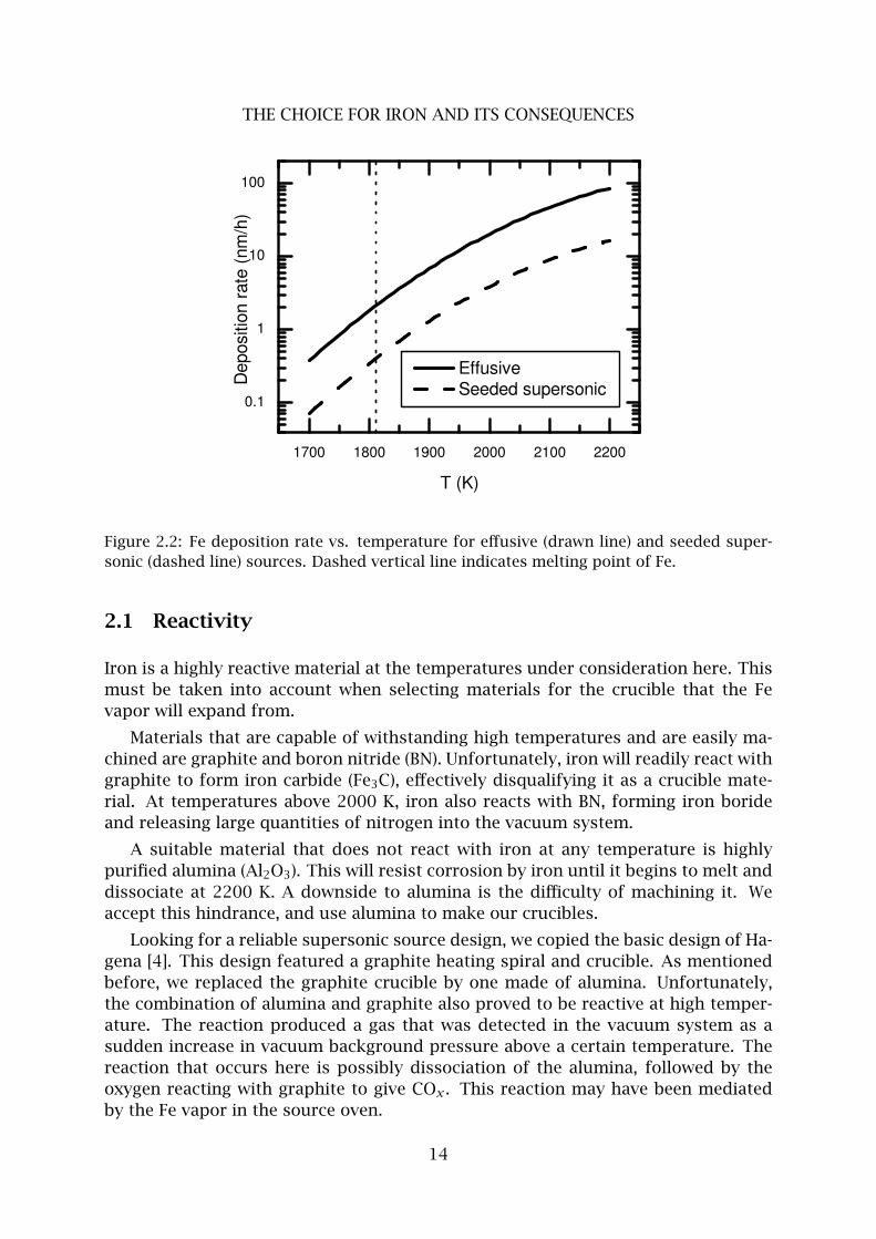
Ferromagnetic nanostructures can only be made from a single atomic species if a fer-
romagnetic element is used. The only elements that are consistently ferromagnetic
at room temperature are iron, nickel, and cobalt.
Table I shows the relevant properties of the three ferromagnetic transition met-
als. Investigating the magnetic properties, we find that the magnetization of Ni is
clearly smaller than that of the other two elements. Experiments investigating these
magnetic nanostructures could suffer from this smaller magnetization. Hence, we
prefer to use another element.
Looking at the atom optical properties of the candidate materials, we find that
the all candidates have a dominant isotope with an abundance of at least 68 %. This
implies that the majority of the atomic beam can be addressed by laser manipulation
with a single laser.
However, the atom optical properties of Co are disastrous. The wavelength of
its only transition suitable for laser cooling is deep in the UV, in a region that is
only accessible with the use of two frequency doubling stages, or doubling a blue
dye laser. In addition, laser cooling results in a very broad velocity distribution due
to the large natural line width. And worst, it would require many repumping laser
systems. The nuclear spin of the only stable isotope, 59Co, is 7/2, generating an
complicated hyperfine spectrum that contains no less than eighty Zeeman states.
The other candidates Fe and Ni are better, though they still present problems. In
the case of Ni, these are mainly inconveniences. Light at the wavelength of Ni can
only be made in sufficient amounts by frequency doubling a dye laser. The dye laser
11
THE CHOICE FOR IRON AND ITS CONSEQUENCES
would then be required to have a frequency stability and line width of better than
500 kHz to stay within one natural line width.
The Fe atom presents a more fundamental problem, namely, the fact that it does
not have a closed transition from the ground state. The 5F5 excited state can decay to
three intermediate states. These states have lifetimes of many milliseconds, which is
effectively infinite in an atom lithography experiment. The Doppler temperature of
Fe is 62 µK, corresponding to a velocity spread of 96 mm/s. Simulations [1] of laser
cooling using this leaky transition show that a suitably narrow-band laser system
would be able to achieve a collimation close to this value.
In conclusion, we find that Fe is the most promising magnetic candidate mate-
rial for atom lithography. Atom lithography is virtually impossible using Co. The
choice between Fe and Ni is motivated mainly by the greater saturation magnetiza-
tion and isotopic purity of Fe. The more cumbersome laser system that would be
needed for Ni should be weighed against the complication of laser cooling with a
leaky transition.
Table I: Properties of the ferromagnetic elements Fe, Co and Ni.
Fe Co Ni
magnetic properties
atomic magn. moment (µB) 4 3 2
bulk magn. moment (µB) 2.2 1.7 0.6
bulk phase crystal structure bcc hcp fcc
magnetization µ0Ms (T) 2.16 1.72 0.61
Curie temperature (K) 1044 1393 628
isotopes
Z 26 27 28
most abundant 56Fe 92% 59Co 100% 58Ni 68%
other isotopes 54Fe 6% 60Ni 26%57Fe 2% 62Ni 4%
61Ni 1%64Ni 1%
atomic properties
electron conf. 3d64s2 3d74s2 3d84s2
ground state conf. 5D44F9/2
3F4
ground state J 4 9/2 4
nuclear spin I 0 (56Fe) 7/2 (59Co) 0 (58Ni)
ground state pop. @ 2000 K 50% 12% 70%
atomic transitions from ground state
transition 5D4 →5 F54F9/2 →4 G11/2
3F4 →3 G5
wavelength (nm) 372.0 240.5 323.4
Γ upper state (MHz) 2.58 57.3 1.16
saturation intens. Is (W/m2) 62 5156 43
leak rate 1:243 0 0
12
FE SOURCE
1500 2000
-8
-6
-4
-2
0
log
P (
mba
r)
T (K)
Figure 2.1: Vapor pressure of Fe. Data from Ref. [10]. Vertical line indicates melting point
(1811 K).
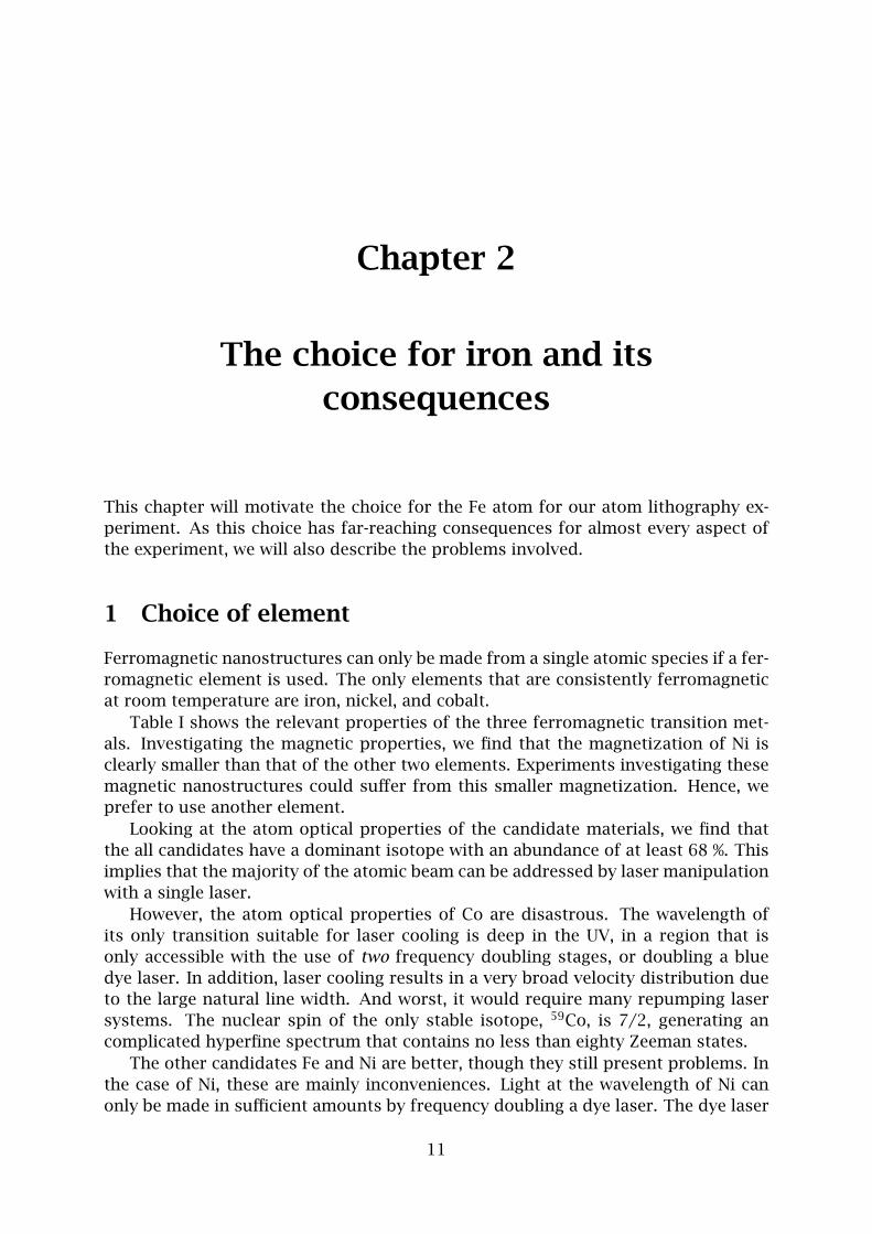
2 Fe source
We need a source of iron atoms that will generate a sufficient flux of ground state Fe
atoms. Therefore, we must heat Fe to a temperature at which its vapor pressure is
sufficient for our demands. Figure 2.1 shows the vapor pressure of Fe as a function
of temperature.
Ideally, we aim for a supersonic beam source to minimize the longitudinal ve-
locity spread of the Fe beam. For an expansion to become supersonic at zero back-
ground pressure, the Knudsen number in the orifice must be much smaller than one.
The Knudsen number Kn is defined as the mean free path λ divided by the orifice
diameter d:
Kn ≡ λ
d= 1
n√
2σd. (2.1)
The collision cross-section for Fe-Fe collisions is estimated at σ = 0.5 nm2, and the
atom density n can be derived from the ideal gas law. Around 2000 K, Kn is one
for a vapor pressure of 0.4 mbar. Although this temperature and pressure might
be feasible, a properly supersonic expansion would require a much higher pressure,
which is impossible to achieve by Fe vapor pressure alone.
This consideration led us to investigate the possibility of a seeded supersonic
expansion [2]. Letting the iron vapor mix with a high-pressure inert gas that sub-
sequently undergoes a supersonic expansion means that the velocity distribution of
the Fe will become similar to that of the Ar [3]. The other option is using an effusive
Fe source.
13
THE CHOICE FOR IRON AND ITS CONSEQUENCES
1700 1800 1900 2000 2100 2200
0.1
1
10
100
Effusive Seeded supersonic
Dep
ositi
on r
ate
(nm
/h)
T (K)
Figure 2.2: Fe deposition rate vs. temperature for effusive (drawn line) and seeded super-
sonic (dashed line) sources. Dashed vertical line indicates melting point of Fe.
2.1 Reactivity
Iron is a highly reactive material at the temperatures under consideration here. This
must be taken into account when selecting materials for the crucible that the Fe
vapor will expand from.
Materials that are capable of withstanding high temperatures and are easily ma-
chined are graphite and boron nitride (BN). Unfortunately, iron will readily react with
graphite to form iron carbide (Fe3C), effectively disqualifying it as a crucible mate-
rial. At temperatures above 2000 K, iron also reacts with BN, forming iron boride
and releasing large quantities of nitrogen into the vacuum system.
A suitable material that does not react with iron at any temperature is highly
purified alumina (Al2O3). This will resist corrosion by iron until it begins to melt and
dissociate at 2200 K. A downside to alumina is the difficulty of machining it. We
accept this hindrance, and use alumina to make our crucibles.
Looking for a reliable supersonic source design, we copied the basic design of Ha-
gena [4]. This design featured a graphite heating spiral and crucible. As mentioned
before, we replaced the graphite crucible by one made of alumina. Unfortunately,
the combination of alumina and graphite also proved to be reactive at high temper-
ature. The reaction produced a gas that was detected in the vacuum system as a
sudden increase in vacuum background pressure above a certain temperature. The
reaction that occurs here is possibly dissociation of the alumina, followed by the
oxygen reacting with graphite to give COx. This reaction may have been mediated
by the Fe vapor in the source oven.
14
FE SOURCE
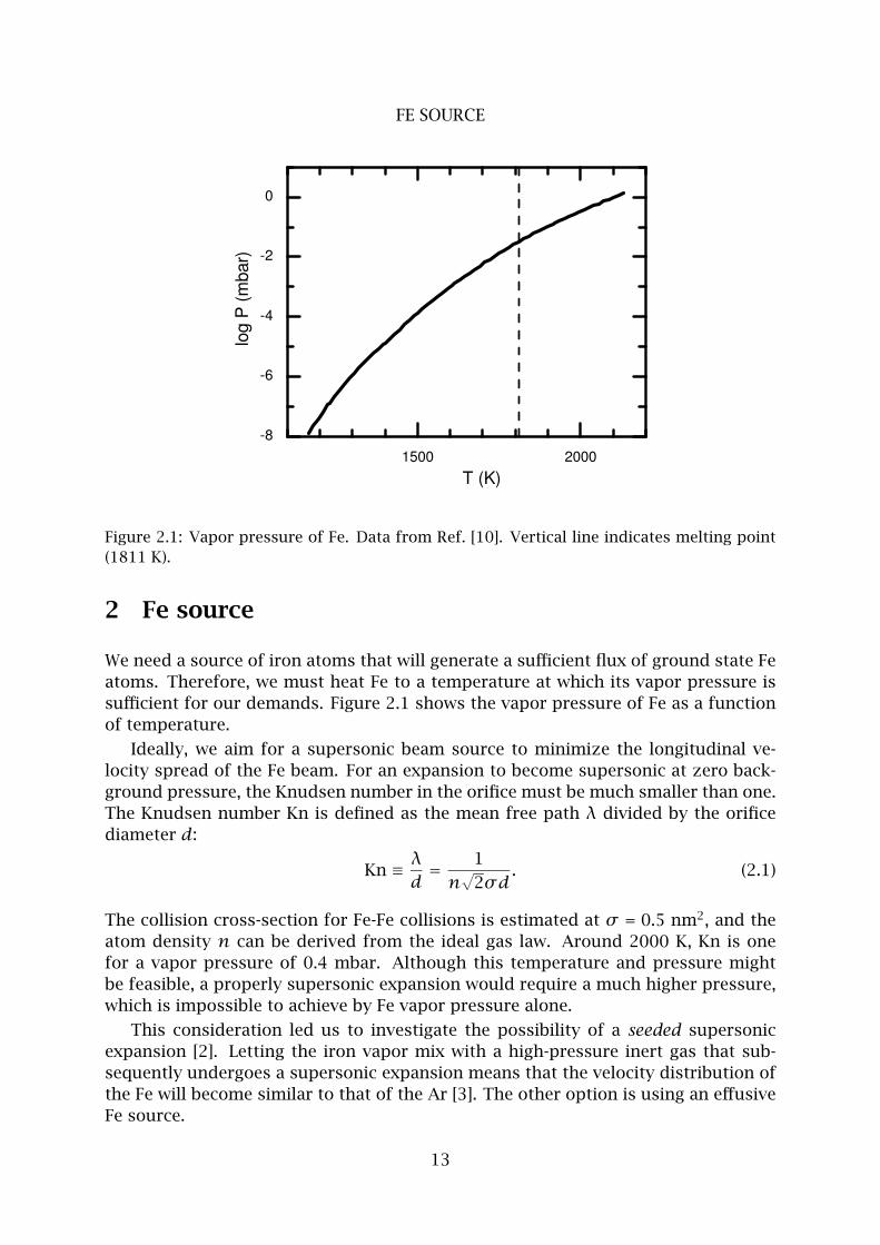
2.2 Crucible design
As the Fe is liquid at typical operating temperatures, it is free to move through the
crucible. This problem does not occur for Cr. As the droplet usually lies on a hori-
zontal surface, it will generally not flow, but it may creep. This creep is apparently
induced by temperature gradients, and was found always to go in the direction of
lowest temperature.
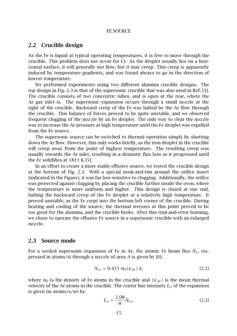
We performed experiments using two different alumina crucible designs. The
top design in Fig. 2.3 is that of the supersonic crucible that was also used in Ref. [3].
The crucible consists of two concentric tubes, and is open at the rear, where the
Ar gas inlet is. The supersonic expansion occurs through a small nozzle at the
right of the crucible. Backward creep of the Fe was halted by the Ar flow through
the crucible. This balance of forces proved to be quite unstable, and we observed
frequent clogging of the nozzle by an Fe droplet. The only way to clear the nozzle
was to increase the Ar pressure at high temperature until the Fe droplet was expelled
from the Fe source.
The supersonic source can be switched to thermal operation simply by shutting
down the Ar flow. However, this only works briefly, as the iron droplet in the crucible
will creep away from the point of highest temperature. The resulting creep was
usually towards the Ar inlet, resulting in a dramatic flux loss as it progressed until
the Fe solidifies at 1811 K [5].
In an effort to create a more stable effusive source, we tested the crucible design
at the bottom of Fig. 2.3. With a special nook-and-rim around the orifice insert
(indicated in the Figure), it was far less sensitive to clogging. Additionally, the orifice
was protected against clogging by placing the crucible further inside the oven, where
the temperature is more uniform and higher. This design is closed at one end,
halting the backward creep of the Fe droplet at a relatively high temperature. It
proved unstable, as the Fe crept into the bottom left corner of the crucible. During
heating and cooling of the source, the thermal stresses at this point proved to be
too great for the alumina, and the crucible broke. After this trial-and-error learning,
we chose to operate the effusive Fe source in a supersonic crucible with an enlarged
nozzle.
2.3 Source mode
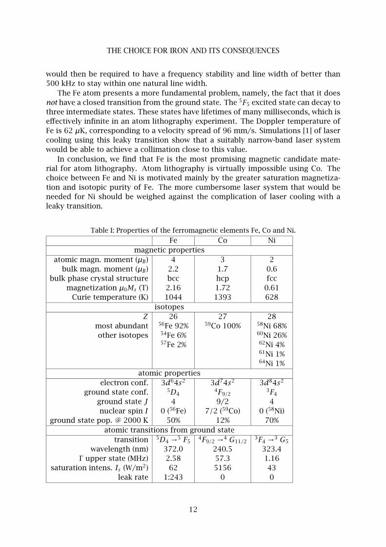
For a seeded supersonic expansion of Fe in Ar, the atomic Fe beam flux Nss (ex-
pressed in atoms/s) through a nozzle of area A is given by [6]:
Nss = 0.455 n0〈vAr〉A, (2.2)
where n0 is the density of Fe atoms in the crucible and 〈vAr〉 is the mean thermal
velocity of the Ar atoms in the crucible. The center line intensity Iss of the expansion
is given (in atoms/s/sr) by:
Iss =2.08
πNss . (2.3)
15
THE CHOICE FOR IRON AND ITS CONSEQUENCES
10 mm
Figure 2.3: Seeded supersonic mode crucible (top) and effusive mode crucible (bottom).
Dashed line indicates position of temperature maximum. Arrow points to anti-clogging rim
around orifice.
Expressed in terms of the properties of the Fe atoms in the crucible for comparison
with an effusive source, this expression reads:
Iss =4.31
4πn0〈vFe〉A. (2.4)
Here, 〈vFe〉 =√
8kT/πmFe is the mean thermal velocity of the Fe atoms in the cru-
cible. To achieve a satisfactory velocity distribution (σv/〈v〉 < 0.1), the expansion
must to operate at an Ar pressure over 100 mbar. Such an expansion imposes a huge
gas load on the vacuum system; we found that it was necessary to limit the nozzle
diameter to 0.23 mm. The calculated deposition rate at a sample located 0.6 m from
the nozzle from such a source is shown in Fig. 2.2 (dashed line). The velocity spread
σv/〈v〉 is typically around 0.07 for this supersonic expansion [3].
The Fe flux from the orifice of an effusive source can be estimated by assuming
that the Fe vapor inside the crucible is in thermal equilibrium. The total atom flux
Nth is given by:
Nth =1
4n0〈vFe〉A. (2.5)
The intensity of the thermal beam Ith is then given by:
Ith =1
πNth =
1
4πn0〈vFe〉A. (2.6)
The non-supersonic expansion of the Fe in the vacuum system has two effects. First,
the difference between a supersonic expansion and effusive flow results a factor 4.31
flux loss. However, the orifice diameter can be increased to 1 mm, as determined by
the acceptance of the rest of the setup. This leads to a factor 20 gain in flux. The net
effect is that the thermal effusive source yields 4.5 times more flux than the seeded
supersonic source. A theoretical calculation of this flux at 0.6 m from the nozzle is
shown in Fig. 2.2 (drawn line). For a purely effusive source, the longitudinal velocity
distribution is of the shape:
P(v/α) = 2∗ (v/α)3 exp−(v/α)2, (2.7)
16
SAMPLES
α =√
2kT/m being the most probable velocity of the Fe atoms in the source. This
distribution yields a velocity spread σv/〈v〉 = 0.36, a factor five more than the su-
personic source.
It is clear that the supersonic source works well to suppress the longitudinal
velocity spread of the Fe beam. However, the seeded supersonic expansion places
a tremendous gas load on the vacuum system. In the source chamber, a 50 l/s
roots blower had to be used instead of a turbomolecular pump, meaning far higher
background pressures and much more contamination throughout the entire vacuum
system. We conclude that the loss of beam intensity, the difficulty of making the
supersonic source function reliably, and the tremendous gas load on the vacuum
system clearly outweigh the benefits of the supersonic velocity distribution. For the
remainder of this thesis, we will work with the effusive source exclusively.
3 Samples
For the experiments described in this thesis, the sample was simply a piece of Si[100]
wafer, with the native oxide layer still intact. However, for better study of the sub-
strate dependence of the deposition experiments, we have also included the option
of using monocrystalline samples. The crystals to be used are W[110] crystals, as
these were shown to have a high activation energy for surface diffusion of atomic
Fe [7].
The 4 × 4 × 1 mm samples were prepared in the MMN group of Janssen by
annealing a monocrystalline piece of W in an oxygen environment at 1600 C for
five hours [8]. After cutting and polishing, the samples were ready for use. A
quick isotropic NaOH electrolytic etch was used to remove any metallic and organic
residues on the sample, and the clean sample was placed into the vacuum system. A
final cleaning stage takes place in vacuo, by annealing at 500 C for several minutes.
This treatment ensures a clean W surface, ready for deposition [8].
For the annealing phase, an electron gun was used that was integrated into the
sample assembly. In the sample holder, the sample rests on a Macor slab that serves
was used to electrically isolate the W sample from the rest of the vacuum system. A
∼ 1 kV bias voltage can thus be applied to the sample to extract an electron current
of up to several mA from a nearby W filament. This current can heat the sample up
to 500 C.
4 Corrosion protection
As the deposition setup does not include the possibility of in situ sample diagnos-
tics, we need to remove the samples from the vacuum system. Once outside, the iron
we have deposited will rapidly corrode. As the corrosion product - most likely rust
(Fe2O3) - is not ferromagnetic, this is highly undesirable. We protect the magnetic
nanostructures by covering them with a capping layer. This layer seals the nanos-
tructures from the atmosphere, preventing oxidation and preserving their magnetic
17
THE CHOICE FOR IRON AND ITS CONSEQUENCES
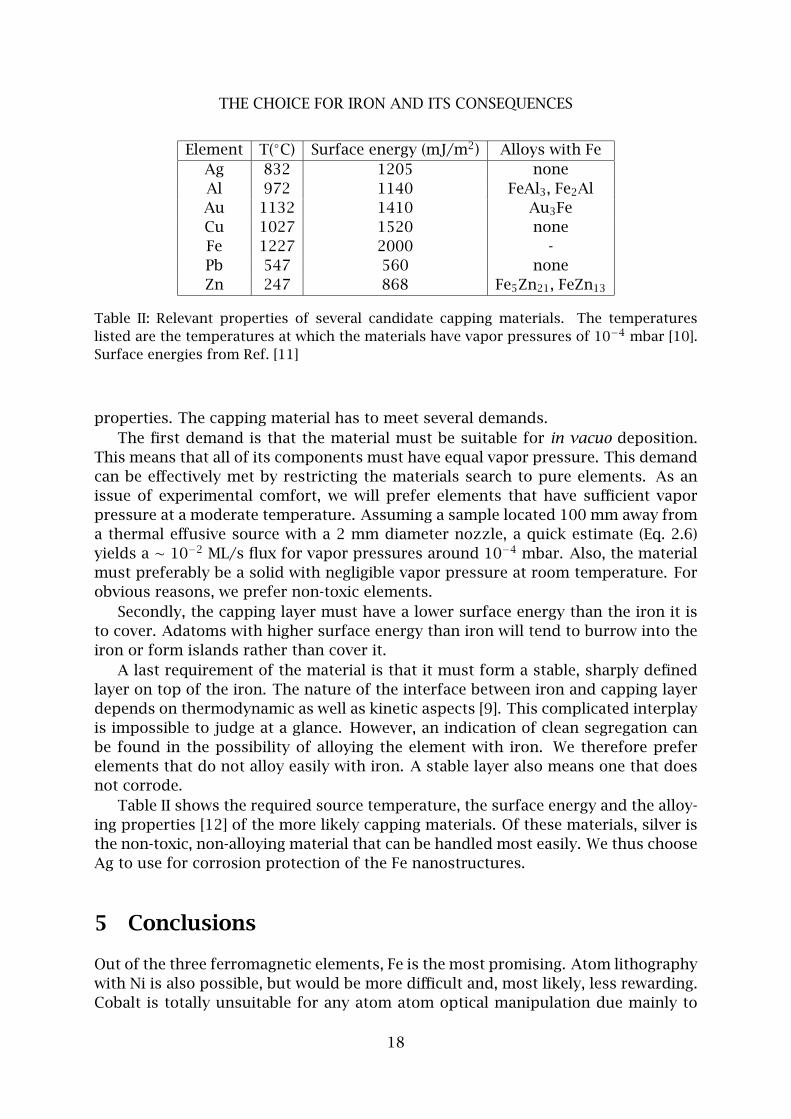
Element T(C) Surface energy (mJ/m2) Alloys with Fe
Ag 832 1205 none
Al 972 1140 FeAl3, Fe2Al
Au 1132 1410 Au3Fe
Cu 1027 1520 none
Fe 1227 2000 -
Pb 547 560 none
Zn 247 868 Fe5Zn21, FeZn13
Table II: Relevant properties of several candidate capping materials. The temperatures
listed are the temperatures at which the materials have vapor pressures of 10−4 mbar [10].
Surface energies from Ref. [11]
properties. The capping material has to meet several demands.
The first demand is that the material must be suitable for in vacuo deposition.
This means that all of its components must have equal vapor pressure. This demand
can be effectively met by restricting the materials search to pure elements. As an
issue of experimental comfort, we will prefer elements that have sufficient vapor
pressure at a moderate temperature. Assuming a sample located 100 mm away from
a thermal effusive source with a 2 mm diameter nozzle, a quick estimate (Eq. 2.6)
yields a ∼ 10−2 ML/s flux for vapor pressures around 10−4 mbar. Also, the material
must preferably be a solid with negligible vapor pressure at room temperature. For
obvious reasons, we prefer non-toxic elements.
Secondly, the capping layer must have a lower surface energy than the iron it is
to cover. Adatoms with higher surface energy than iron will tend to burrow into the
iron or form islands rather than cover it.
A last requirement of the material is that it must form a stable, sharply defined
layer on top of the iron. The nature of the interface between iron and capping layer
depends on thermodynamic as well as kinetic aspects [9]. This complicated interplay
is impossible to judge at a glance. However, an indication of clean segregation can
be found in the possibility of alloying the element with iron. We therefore prefer
elements that do not alloy easily with iron. A stable layer also means one that does
not corrode.
Table II shows the required source temperature, the surface energy and the alloy-
ing properties [12] of the more likely capping materials. Of these materials, silver is
the non-toxic, non-alloying material that can be handled most easily. We thus choose
Ag to use for corrosion protection of the Fe nanostructures.
5 Conclusions
Out of the three ferromagnetic elements, Fe is the most promising. Atom lithography
with Ni is also possible, but would be more difficult and, most likely, less rewarding.
Cobalt is totally unsuitable for any atom atom optical manipulation due mainly to
18
CONCLUSIONS
its complex hyperfine structure.
Constructing a source for an intense Fe beam is a very difficult task, especially if
the beam line is to be aligned horizontally. However, it is possible. Using a seeded
supersonic beam to reduce the longitudinal velocity spread of the Fe beam is also
possible, but only at the expense of Fe flux and source reliability.
Taking an interest in nanostructure broadening through surface diffusion, we
have the option of using W [110] samples for substrates.
As the Fe nanostructures need to be protected from corrosion, a capping layer
must be applied in situ. A suitable material for this capping layer is Ag.
References
[1] B. Smeets, R. W. Herfst, P. van der Straten, E. te Sligte, H. C. W. Beijerinck, and K. A. H.
van Leeuwen, manuscript in preparation
[2] R. C. M. Bosch, PhD thesis, TU/e (2002)
[3] R. C. M. Bosch, H. C. W. Beijerinck, P. van der Straten, and K. A. H. van Leeuwen, Eur.
Phys. J. A. P. 18, 221-227 (2002)
[4] O. F. Hagena, Z. Phys. D 20, 425 (1991)
[5] CRC Handbook of Chemistry and Physics, 84th Ed. (CRC Press, Boca Raton, 2003)
[6] H. C. W. Beijerinck and N. Verster, Physica 111 C, 327-352 (1981)
[7] D.Spisak and J. Hafner, Phys. Rev. B 70, 195426 (2004)
[8] R. Cortenraad, S. N. Ermolov, V. N. Semenov, A. W. Denier van der Gon, V. G. Glebovsky,
S. I. Bozhko, and H. H. Brongersma, J. Crystal Growth 222, 154-162 (2001)
[9] H. Luth, Surfaces and Interfaces of Solid Materials, 3rd ed., Springer (1997)
[10] R. E. Honig and D. A. Kramer, RCA Review 30, 285-305 (1969)
[11] V. K. Kumikov and Kh. B. Khokonov, J. Appl. Phys. 54, 1346-1349 (1983)
[12] Search for alloys and compounds performed using www.google.com
19

THE CHOICE FOR IRON AND ITS CONSEQUENCES
20
Chapter 3
Atoms in standing waves
The description of the atom-light interaction in terms of classical induced dipole
moments given in the introduction suffices to understand that standing waves can
act as lenses on atoms. However, it is not enough to understand all the experiments
discussed in this thesis. Hence, we need to discuss a more refined theory, specifically
the dressed state model [2]. We will first outline the theory, and then investigate its
implications for atom lithography experiments. This chapter is intended mainly to
help the reader understand the simulations and experiments done in Chapters 5
and 7.
1 Theory
An atom in a light field close to a resonance will absorb and re-emit photons. The
re-emission can occur in two ways: the atom can decay spontaneously to its ground
state, or it can undergo stimulated emission. The model discussed here seeks to
describe the effect of all stimulated emissions as a semiclassical dipole potential;
spontaneous emission is considered separately later on.
1.1 The semiclassical approximation
This approach is valid if the atom can be considered as a point particle that moves
through a potential landscape with a well-defined velocity. This means that the wave
nature of the atom can be neglected when considering its center-of-mass motion.
Hence, the position uncertainty of the atom must be much smaller than the wave-
length λ of the light. Taking the De Broglie wavelength λDB as a measure of this
uncertainty:
λDB ≪ λ. (3.1)
For iron atoms moving at 1000 m/s, λDB = 7 pm, and λDB/λ ≈ 2×10⁻⁵. However, the
diffraction limit for atom optics is far greater than the De Broglie wavelength, as the
numerical aperture of the lenses is very small. Typical values are around 10 nm [1].
21
ATOMS IN STANDING WAVES
In this context, the uncertainty in the velocity ∆(v) is effectively small if the
uncertainty in the Doppler shift it induces is much smaller than the natural linewidth
Γ = 2π × 2.58 MHz of the transition:
k∆(v)≪ Γ , (3.2)
with k the wave number of the laser light. The velocity uncertainty is of the order
of one recoil kick k/m = 0.02 m/s. This yields a Doppler shift of 0.02 Γ . We thus
conclude that the position and velocity of the atom are well-defined, and that it may
be considered as a point particle.
1.2 Dressed states
The dressed state model discussed here was first introduced by Dalibard and Cohen-
Tannoudji in 1985 [2]. The adjective “dressed” refers to the fact that one considers
not the eigenstates of the atom but rather those of the complete atom-light field
system.
A stationary atom in a light field will have a Hamiltonian of the form:
H = Hatom +Hlight +Hint, (3.3)
which is nothing more than saying that there will be energy contributions from the
state of the atom (Hatom), the state of the light field (Hlight), and the interaction
between the two (Hint). We assume that the atom is a two-level atom, though the
approach also works for more complicated atomic structures. The internal energy
of the atom is zero in the ground state, and ω0 in the excited state.
The frequency of the laser ωL is assumed to be such that |ωL −ω0| ≪ ω0. The
energy eigenvalues of the light field are En = (n + 12)ωL, with n the number of
photons in the light field. This is a “ladder” of states separated by ωL, as shown in
Fig. 3.1(a). If we now include the atom in the Hamiltonian, we get a ladder of pairs
of states. For blue detuning (∆ = ωL −ω0 > 0), the ladder is shown in Fig. 3.1(b).
The separation between the states in a pair is equal to ∆, much smaller than the
separation between the pairs ωL.
These states become dressed when the interaction between the atom and the light
field is taken into account. This interaction mixes the states of the light field and the
atom and shifts the eigenenergies of the system. The coupling between the atom and
the light field takes place almost entirely within a pair of states on the ladder, and
can be characterized by the Rabi frequency ωR and the phase φ of the light field.
The Rabi frequency is related to the intensity of the light field by ωR = Γ√
I/2Is .
After solving for the eigenstates and eigenenergies of the complete system, Dalibard
and Cohen-Tannoudji find that for each n, there is a pair of eigenstates with:
En,+ = (n+ 1)ωL −δ
2+ Ω
2,
En,− = (n+ 1)ωL −δ
2− Ω
2. (3.4)
22
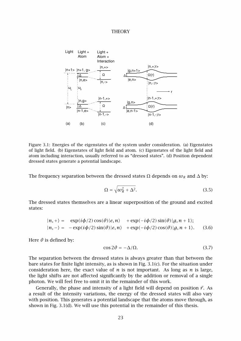
THEORY
(d)
ω0
Light +Atom + Interaction
Light +Atom
Light
|g,n+1>Ω
r
(c)(b)(a)
|n+1>
|n>
ωL
Ω
|n-1,->
|n-1,+>
|n,->
|n,+>
|n-1,e>
|n,g>
|n,e>
|n+1, g>
∆
∆
|e,n-1>
|g,n>
|e,n>
|n-1,-;r>
|n-1,+;r>
|n,-;r>
|n,+;r>
∆
∆
Ω(r)
Ω(r)
Figure 3.1: Energies of the eigenstates of the system under consideration. (a) Eigenstates
of light field. (b) Eigenstates of light field and atom. (c) Eigenstates of the light field and
atom including interaction, usually referred to as “dressed states”. (d) Position dependent
dressed states generate a potential landscape.
The frequency separation between the dressed states Ω depends on ωR and ∆ by:
Ω =√
ω2R +∆2. (3.5)
The dressed states themselves are a linear superposition of the ground and excited
states:
|n,+〉 = exp(iφ/2) cos(θ)|e,n〉 + exp(−iφ/2) sin(θ)|g,n+ 1〉;|n,−〉 = − exp(iφ/2) sin(θ)|e,n〉 + exp(−iφ/2) cos(θ)|g,n+ 1〉. (3.6)
Here θ is defined by:
cos 2θ = −∆/Ω. (3.7)
The separation between the dressed states is always greater than that between the
bare states for finite light intensity, as is shown in Fig. 3.1(c). For the situation under
consideration here, the exact value of n is not important. As long as n is large,
the light shifts are not affected significantly by the addition or removal of a single
photon. We will feel free to omit it in the remainder of this work.
Generally, the phase and intensity of a light field will depend on position ~r . As
a result of the intensity variations, the energy of the dressed states will also vary
with position. This generates a potential landscape that the atoms move through, as
shown in Fig. 3.1(d). We will use this potential in the remainder of this thesis.
23
ATOMS IN STANDING WAVES
1.3 Spontaneous emission
Not included in the dressed states are the effects of spontaneous emission. This
process is a transition from the excited state to the ground state, during which n
decreases by one. The rate at which an atom undergoes spontaneous emissions is
proportional to its excited state population. This population can be derived from
Eq. 3.6. The chance that an atom will end up in a given dressed state is given by
the ground state population of that state. An atom that undergoes a spontaneous
emission thus has a finite chance of remaining in its original dressed state, and a
finite chance of changing dressed state. The transition rates between dressed states
that result from these chances can be expressed in terms of the angle θ defined
above:
Γ+− = Γ cos4 θ; (3.8)
Γ−+ = Γ sin4 θ. (3.9)
After many spontaneous emissions, a balance between the dressed states is formed,
and the effective potential averaged over both dressed states can by described by a
logarithmic function [2]. In the case of atom lithography, this is explicitly not the
correct description. An atom that moves through a 0.1 mm laser beam at 1000 m/s
interacts with the light for some 100 ns. The natural decay time of the transition
under consideration in this thesis is 62 ns. The fact that less than half of the atoms
is in the excited state means that the effective decay time will be more than twice
this value. This means that typically, atoms will undergo zero or one spontaneous
emission events in the course of the entire focusing interaction, hardly enough for
any kind of radiative balance.
In addition, the atom receives a recoil kick in a random direction any time a spon-
taneous emission occurs. The effects of this recoil kick are normally small in atom
lithography. After one recoil at the start of the interaction, the resulting velocity
change of 0.02 m/s, entails a displacement of 2 nm at the end of the interaction.
This is not a significant displacement.
1.4 Moving atoms
The dressed states are eigenstates for stationary atoms. If the atomic center-of-mass
position ~r varies with time, so do the eigenstates of the atom-light system. The atom
can follow these variations adiabatically if its motion, and hence the rate of change
of its eigenstates, is slow enough. If the eigenstates change very quickly, the internal
state of the atom will remain unchanged, and only its description in terms of the
dressed states will change. Viewed from the dressed state perspective, there is a
chance that it is transferred from one dressed state into the other. This is called a
nonadiabatic transition.
An upper limit estimate of the nonadiabatic (NA) transition probability Pi→j be-
tween levels |n, i; ~r〉 and |n, j; ~r〉 can be found in Ref. [3]:
Pi→j ≤ max
|〈n, j; ~r | ddt|n, i; ~r〉|2
|ωij|2
, (3.10)
24
NUMERICAL MODEL
whereωij is the Bohr frequency between levels i and j at time t. In the dressed state
model, |i〉 and |j〉 can be |+〉 or |−〉, and ωij = Ω[~r(t)]. The overlap integral in the
enumerator can be found using Eq. 3.6 assuming constant phase φ:
d
dt|n, i; ~r〉 = d~r
dt· ~∇|n, i; ~r〉 = ±~v · ~∇θ(~r)|n, j; ~r〉. (3.11)
The gradient of θ can be found using Eq. 3.7. If we insert a sine-shaped standing
wave with maximum Rabi frequency ωR,max as the expression for I, we can thus
estimate the NA transition probability as:
Pi→j ≲ max[(~k · ~v
2
)2 |∆ ωR,max cos(~k · ~r)|2
|∆2 +ω2R,max sin2(~k · ~r)|3
]
. (3.12)
From this expression, we can find where the NA transitions are most likely to occur:
around the nodes of the standing wave. The chance for a NA transition when an
atom traverses a node is overestimated by:
Pi→j ≲∣
∣
∣
~k · ~v2
ωR,max
∆2
∣
∣
∣
2(3.13)
Clearly, a large detuning and modest Rabi frequency help limit the amount of NA
transitions. As with the spontaneous emissions, the model treats NA transitions as
a correction in hindsight.
2 Numerical model
We will now proceed to apply the dressed state model described above to atom
lithography. What we seek is a prediction of the atomic flux distribution after the in-
teraction with the light field. To this end, we will solve the equations of motion for a
large number of atoms numerically. We will discuss the results of these simulations.
2.1 Equations of motion
The atoms are classical point particles moving through a potential U . The energy
shift of the atoms as a function of the light field intensity I and detuning ∆ is:
U = ±2
√
I(~r)
2IsΓ 2 +∆2 − ∆
2, (3.14)
where the sign is that of the dressed state the atom is currently in. Calculating the
trajectory of an atom through a light mask is now just a matter of integrating its
Newtonian equation of motion.
We describe our light mask as a one-dimensional Gaussian standing wave, ob-
tained by superposition of two running waves with a waist of width w:
I(~r) = I0 sin2(kx) exp(−2z2
w2). (3.15)
25
ATOMS IN STANDING WAVES
Here k = 2π/λ is the wave number of the running wave, and the atoms are assumed
to move along the z-axis. The central intensity can be described in terms of the
running wave power by I0 = 8P/πw2
Assuming that the atoms’ kinetic energy is much larger than the potential height
of the light mask allows us to neglect its effect on their longitudinal motion. We thus
concentrate on their lateral motion, which is far slower:
Fx = −∂U
∂x=m∂2x
∂t2. (3.16)
As our interest lies in the trajectories of the atoms, we transform from t to z by
introducing vz. If we further introduce dimensionless parameters χ = kx and ζ =z/w, the resulting equation reads:
d2χ
dζ2= ±AB exp(−2ζ2) sin(2χ)
√
1+ B exp(−2ζ2) sin2(χ). (3.17)
Here, we have defined:
A = k2w2|∆|2mv2
z
B = 4PΓ2
πw2Is∆2 =ω2R,max
∆2 (3.18)
On inspection of A, we find that themv2z term is a measure for the kinetic energy
of the atoms. Also, the factor k2w2 can be traced directly to the aspect ratio w/λ
of the potential variations. The ratio mv2z/k
2w2 is a measure for the maximum
kinetic energy of the transverse motion of the atoms that fit within the acceptance
angle of the atom lenses. On the other hand, ∆ is the energy splitting between the
dressed states outside the light mask. Thus, we find that A physically represents the
ratio between the transverse kinetic energy of the atoms that can be focused and the
splitting of the dressed states outside the standing wave.
All the terms that enter into B are related to the light mask itself. The maximum
intensity in the light mask is given by Eq. 3.15, and reappears here. So B can clearly
be interpreted as a measure of the maximum saturation parameter divided by the
detuning expressed in linewidths. In terms of energy,√B measures the maximum
light shift in units of the splitting of the dressed states outside the standing wave.
Outside the standing wave, the intensity I of the light is zero, and the ground
state is |+〉 for ∆ > 0 and |−〉 for ∆ < 0. Unless they undergo a spontaneous or
nonadiabatic transition, they will stay in their initial state, and their trajectory can
be calculated by simply integrating Eq. 3.17.
2.2 Spontaneous emissions
We include the effects of spontaneous emission in the model by evaluating the
chance that an atom has undergone spontaneous emission at set intervals. The
spontaneous decay rate from one dressed state to the other can be obtained from
26
NUMERICAL MODEL
Eq. 3.8. Seeking to express θ in terms of the model parameters, we recall Eq. 3.7.
This can be rewritten as:
sin[2θ(~r)] = B(~r)/√
1+ B(~r)2, (3.19)
with B(~r) = B exp(−2ζ2) sin2(χ). Now, we can obtain an expression for the maxi-
mum spontaneous emission rate in terms of B(~r):
ΓDS(~r) =Γ
2
1+ 12B(~r)±
√
1+ B(~r)1+ B(~r) , (3.20)
where the sign is negative if the signs of the detuning ∆ and the dressed state are
the same. The chance that an atom has undergone a spontaneous emission in time
interval τ is now simply ΓDSτ .
An upper limit to the chance of spontaneous emission during the interaction with
the light mask is given by Γw/vz, as the light mask extends from z = −w to z = w,
and the spontaneous decay rate is Γ/2 at most. This is typically of order unity in our
experiments.
2.3 Non-adiabatic transitions
The probability for non-adiabatic transitions to occur is more difficult to calculate,
and one would be better off simply solving the optical Bloch equations numerically.
However, we can estimate the effects of non-adiabatic transitions crudely. Non-
adiabatic transitions are most likely to occur when atoms cross a node, and so we
state in our model that they occur exclusively when an atom crosses a node.
The estimate for the NA transition probability (Eq. 3.13) can be rewritten in terms
of the numerical model parameters:
Pi→j ≲(kv
2∆
)2B. (3.21)
We set the model NA transition probability to unity if the above estimate is greater
than unity; else, we set it to zero. Though it is only a crude approximation, it is
satisfactory for the present model. For an atom moving with 1 m/s in the x-direction
through a standing wave detuned by 150 MHz, the value of the estimate is unity for
B ∼ 104.
2.4 Calculation
We start with a number of atoms that are homogeneously distributed over a single
wave length in the x-direction. The transverse velocity distribution of a laser cooled
atomic beam is approximately Gaussian [4]; that of an uncooled beam from a round
nozzle can be approximated by a Gaussian. The atoms have a Gaussian transverse
velocity distribution. The longitudinal velocity distribution of the atom beam is that
of an effusive beam (see Ch. 2). The longitudinal velocities are assigned in ascending
order; all other parameters are chosen randomly for each trajectory.
27
ATOMS IN STANDING WAVES
0.0 0.5 1.0 1.5 2.0
-10
-5
0
5
10
|->
|+>
|->
|+>
Ene
rgy
(h∆)
x/λ
0.0 0.5 1.0 1.5 2.0
-1.01
-1.00
-0.99
0.99
1.00
1.01
x/λ
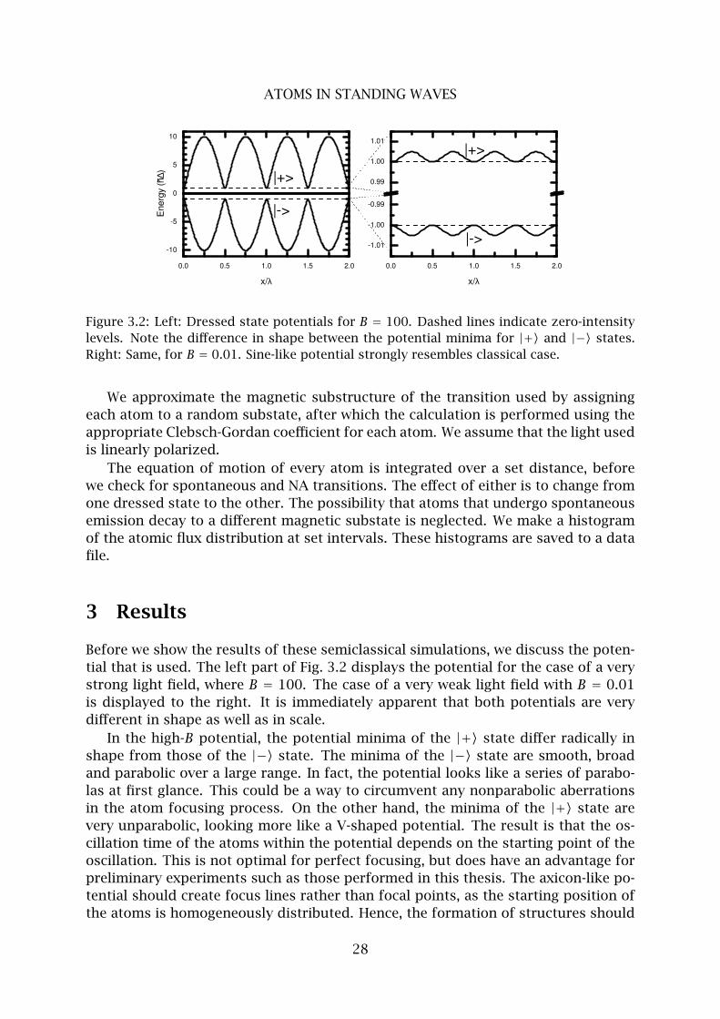
Figure 3.2: Left: Dressed state potentials for B = 100. Dashed lines indicate zero-intensity
levels. Note the difference in shape between the potential minima for |+〉 and |−〉 states.
Right: Same, for B = 0.01. Sine-like potential strongly resembles classical case.
We approximate the magnetic substructure of the transition used by assigning
each atom to a random substate, after which the calculation is performed using the
appropriate Clebsch-Gordan coefficient for each atom. We assume that the light used
is linearly polarized.
The equation of motion of every atom is integrated over a set distance, before
we check for spontaneous and NA transitions. The effect of either is to change from
one dressed state to the other. The possibility that atoms that undergo spontaneous
emission decay to a different magnetic substate is neglected. We make a histogram
of the atomic flux distribution at set intervals. These histograms are saved to a data
file.
3 Results
Before we show the results of these semiclassical simulations, we discuss the poten-
tial that is used. The left part of Fig. 3.2 displays the potential for the case of a very
strong light field, where B = 100. The case of a very weak light field with B = 0.01
is displayed to the right. It is immediately apparent that both potentials are very
different in shape as well as in scale.
In the high-B potential, the potential minima of the |+〉 state differ radically in
shape from those of the |−〉 state. The minima of the |−〉 state are smooth, broad
and parabolic over a large range. In fact, the potential looks like a series of parabo-
las at first glance. This could be a way to circumvent any nonparabolic aberrations
in the atom focusing process. On the other hand, the minima of the |+〉 state are
very unparabolic, looking more like a V-shaped potential. The result is that the os-
cillation time of the atoms within the potential depends on the starting point of the
oscillation. This is not optimal for perfect focusing, but does have an advantage for
preliminary experiments such as those performed in this thesis. The axicon-like po-
tential should create focus lines rather than focal points, as the starting position of
the atoms is homogeneously distributed. Hence, the formation of structures should
28
RESULTS
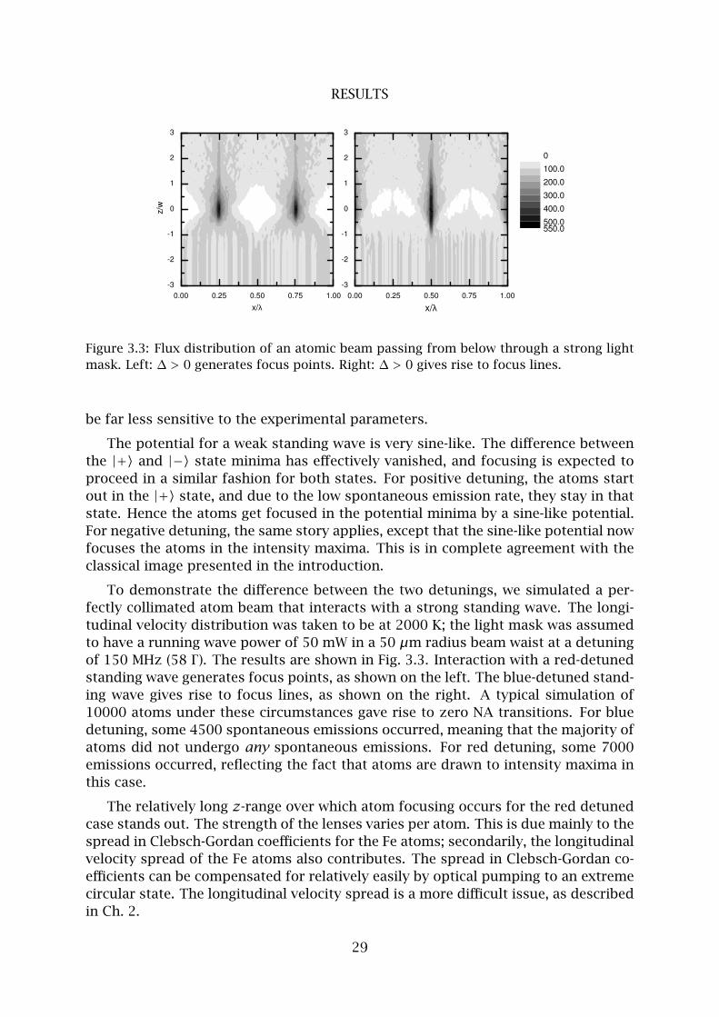
0.00 0.25 0.50 0.75 1.00-3
-2
-1
0
1
2
3
x/λ
z/w
0.00 0.25 0.50 0.75 1.00-3
-2
-1
0
1
2
3
x/λ
0
100.0
200.0
300.0
400.0
500.0550.0
Figure 3.3: Flux distribution of an atomic beam passing from below through a strong light
mask. Left: ∆ > 0 generates focus points. Right: ∆ > 0 gives rise to focus lines.
be far less sensitive to the experimental parameters.
The potential for a weak standing wave is very sine-like. The difference between
the |+〉 and |−〉 state minima has effectively vanished, and focusing is expected to
proceed in a similar fashion for both states. For positive detuning, the atoms start
out in the |+〉 state, and due to the low spontaneous emission rate, they stay in that
state. Hence the atoms get focused in the potential minima by a sine-like potential.
For negative detuning, the same story applies, except that the sine-like potential now
focuses the atoms in the intensity maxima. This is in complete agreement with the
classical image presented in the introduction.
To demonstrate the difference between the two detunings, we simulated a per-
fectly collimated atom beam that interacts with a strong standing wave. The longi-
tudinal velocity distribution was taken to be at 2000 K; the light mask was assumed
to have a running wave power of 50 mW in a 50 µm radius beam waist at a detuning
of 150 MHz (58 Γ ). The results are shown in Fig. 3.3. Interaction with a red-detuned
standing wave generates focus points, as shown on the left. The blue-detuned stand-
ing wave gives rise to focus lines, as shown on the right. A typical simulation of
10000 atoms under these circumstances gave rise to zero NA transitions. For blue
detuning, some 4500 spontaneous emissions occurred, meaning that the majority of
atoms did not undergo any spontaneous emissions. For red detuning, some 7000
emissions occurred, reflecting the fact that atoms are drawn to intensity maxima in
this case.
The relatively long z-range over which atom focusing occurs for the red detuned
case stands out. The strength of the lenses varies per atom. This is due mainly to the
spread in Clebsch-Gordan coefficients for the Fe atoms; secondarily, the longitudinal
velocity spread of the Fe atoms also contributes. The spread in Clebsch-Gordan co-
efficients can be compensated for relatively easily by optical pumping to an extreme
circular state. The longitudinal velocity spread is a more difficult issue, as described
in Ch. 2.
29
ATOMS IN STANDING WAVES
References
[1] C. J. Lee, Phys. Rev. A 61, 063604 (2000); S. J. H. Petra, K. A. H. van Leeuwen, L.
Feenstra, W. Hogervorst, and W. Vassen, Eur. Phys. J. D 27 83-91 (2003).
[2] J. Dalibard and C. Cohen-Tannoudji, J. Opt. Soc. Am. B 2, 1707-1720 (1985)
[3] A. Messiah, Mecanique Quantique II, Dunod, Paris (1964)
[4] H. Metcalf and P. van der Straten, Laser Cooling and Trapping, Springer Verlag,
Heidelberg (1999)
30
Chapter 4
Experimental apparatus
In this chapter, the experimental setup is described that is used to deposit the Fe
nanostructures. This setup must fulfill a number of criteria. It must obviously con-
tain an Fe evaporation source, and must provide for both laser cooling and the in-
teraction with the light mask. A laser system has to provide the necessary light for
both. Finally, it must allow for application of a capping layer in vacuo to protect the
nanostructures from oxidation.
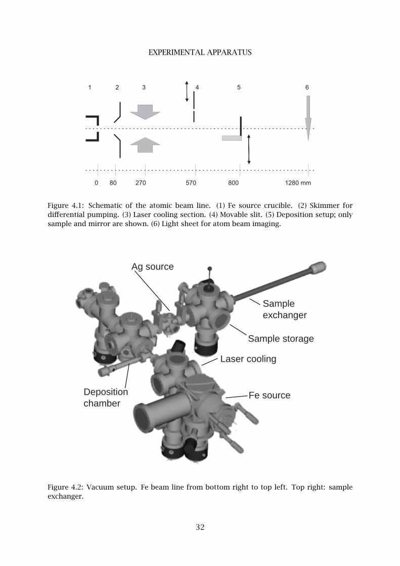
A schematic overview of the atomic beam line is given in Fig. 4.1. The atoms
exit the source (1) and pass through a 2 mm diameter aperture (2) before being
collimated in the laser cooling section (3). For alignment and diagnostic purposes, a
removable 10 µm slit (4) has been installed between the laser cooling and deposition
sections. The atoms are deposited onto a substrate (5) in the deposition chamber.
Finally, imaging of the atomic beam is possible with a light sheet and CCD camera
(6) at the end of the beam line.
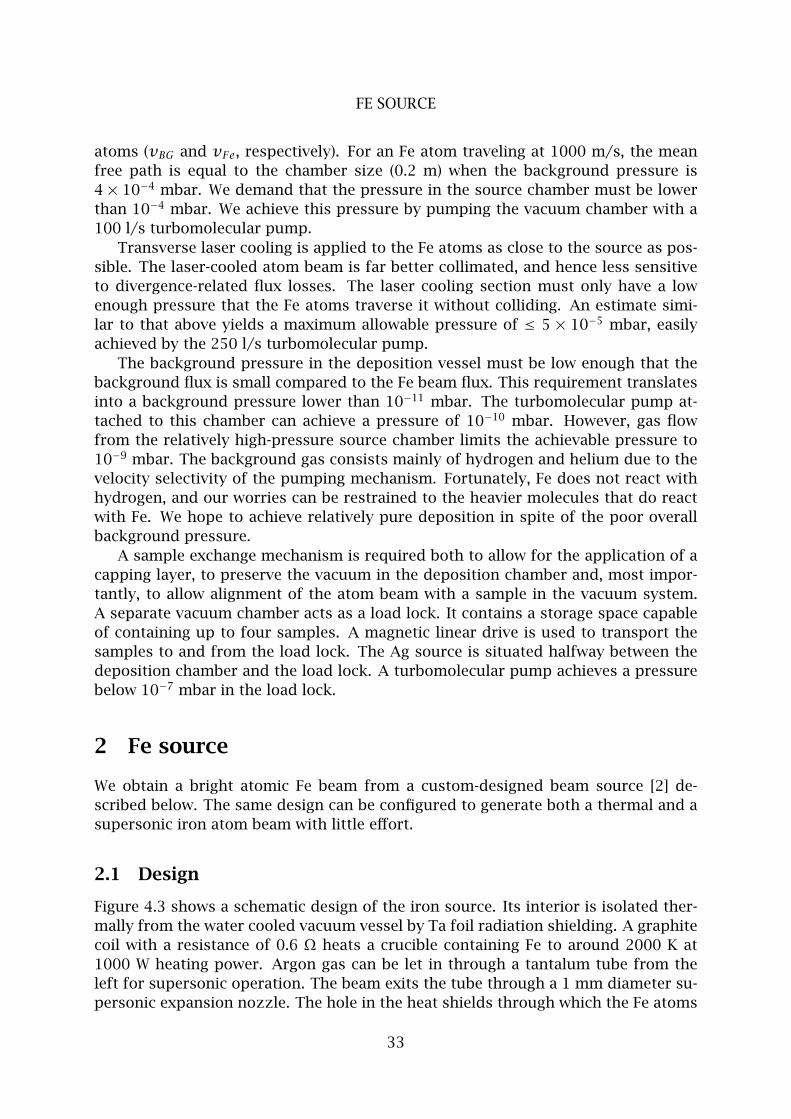
1 Vacuum system
We choose to house the three beam line sections in different stainless steel vacuum
chambers, allowing for differential pumping. Also, we add a load lock so that sam-
ples may be brought into the deposition chamber without breaking its vacuum. An
overview of the vacuum setup is shown in Fig. 4.2.
The evaporation source is located in a separate vacuum chamber. In effusive
mode, the background pressure in the source chamber must be low enough that
the Fe atoms that leave the source do not collide with background gas atoms as
they traverse the chamber. The mean free path of the Fe atoms λ with respect to
collisions with background gas is given by [1]:
λ = 1
nσvrelvFe
, (4.1)
where n is the background gas atomic number density, and σ is the collision cross-
section. We estimate σ at 0.5 nm2. The relative velocity of the atoms vrel =√
v2BG + v2
Fe depends on the velocities of the background gas molecules and the Fe
31
EXPERIMENTAL APPARATUS
Figure 4.1: Schematic of the atomic beam line. (1) Fe source crucible. (2) Skimmer fordifferential pumping. (3) Laser cooling section. (4) Movable slit. (5) Deposition setup; onlysample and mirror are shown. (6) Light sheet for atom beam imaging.
Fe sourceDepositionchamber
Ag source
Sample exchanger
Sample storage
Laser cooling
Figure 4.2: Vacuum setup. Fe beam line from bottom right to top left. Top right: sampleexchanger.
32
FE SOURCE
atoms (vBG and vFe, respectively). For an Fe atom traveling at 1000 m/s, the mean
free path is equal to the chamber size (0.2 m) when the background pressure is
4 × 10⁻⁴ mbar. We demand that the pressure in the source chamber must be lower
than 10−4 mbar. We achieve this pressure by pumping the vacuum chamber with a
100 l/s turbomolecular pump.
Transverse laser cooling is applied to the Fe atoms as close to the source as pos-
sible. The laser-cooled atom beam is far better collimated, and hence less sensitive
to divergence-related flux losses. The laser cooling section must only have a low
enough pressure that the Fe atoms traverse it without colliding. An estimate simi-
lar to that above yields a maximum allowable pressure of ≤ 5 × 10⁻⁵ mbar, easily
achieved by the 250 l/s turbomolecular pump.
The background pressure in the deposition vessel must be low enough that the
background flux is small compared to the Fe beam flux. This requirement translates
into a background pressure lower than 10−11 mbar. The turbomolecular pump at-
tached to this chamber can achieve a pressure of 10−10 mbar. However, gas flow
from the relatively high-pressure source chamber limits the achievable pressure to
10−9 mbar. The background gas consists mainly of hydrogen and helium due to the
velocity selectivity of the pumping mechanism. Fortunately, Fe does not react with
hydrogen, and our worries can be restrained to the heavier molecules that do react
with Fe. We hope to achieve relatively pure deposition in spite of the poor overall
background pressure.
A sample exchange mechanism is required both to allow for the application of a
capping layer, to preserve the vacuum in the deposition chamber and, most impor-
tantly, to allow alignment of the atom beam with a sample in the vacuum system.
A separate vacuum chamber acts as a load lock. It contains a storage space capable
of containing up to four samples. A magnetic linear drive is used to transport the
samples to and from the load lock. The Ag source is situated halfway between the
deposition chamber and the load lock. A turbomolecular pump achieves a pressure
below 10−7 mbar in the load lock.
2 Fe source
We obtain a bright atomic Fe beam from a custom-designed beam source [2] de-
scribed below. The same design can be configured to generate both a thermal and a
supersonic iron atom beam with little effort.
2.1 Design
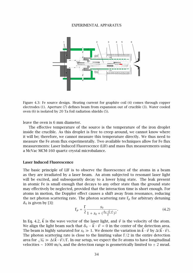
Figure 4.3 shows a schematic design of the iron source. Its interior is isolated ther-
mally from the water cooled vacuum vessel by Ta foil radiation shielding. A graphite
coil with a resistance of 0.6 Ω heats a crucible containing Fe to around 2000 K at
1000 W heating power. Argon gas can be let in through a tantalum tube from the
left for supersonic operation. The beam exits the tube through a 1 mm diameter su-
personic expansion nozzle. The hole in the heat shields through which the Fe atoms
33
EXPERIMENTAL APPARATUS
I
3 5 642 1
Figure 4.3: Fe source design. Heating current for graphite coil (4) comes through copper
electrodes (1). Aperture (7) defines beam from expansion out of crucible (3). Water cooled
oven (6) is isolated by 20 Ta foil radiation shields (5).
leave the oven is 6 mm diameter.
The effective temperature of the source is the temperature of the iron droplet
inside the crucible. As this droplet is free to creep around, we cannot know where
it will be; therefore, we cannot measure this temperature directly. We thus need to
measure the Fe atom flux experimentally. Two available techniques allow for Fe flux
measurements: Laser Induced Fluorescence (LIF) and mass flux measurements using
a McVac MCM-160 quartz crystal microbalance.
Laser Induced Fluorescence
The basic principle of LIF is to observe the fluorescence of the atoms in a beam
as they are irradiated by a laser beam. An atom subjected to resonant laser light
will be excited, and subsequently decay to a lower lying state. The leak present
in atomic Fe is small enough that decays to any other state than the ground state
may effectively be neglected, provided that the interaction time is short enough. For
atoms in motion, the Doppler effect causes a shift away from resonance, reducing
the net photon scattering rate. The photon scattering rate Γp for arbitrary detuning
δ0 is given by [3]:
Γp =Γ
2
s0
1+ s0 + (δ0−~k·~vΓ
)2. (4.2)
In Eq. 4.2, ~k is the wave vector of the laser light, and ~v is the velocity of the atom.
We align the light beam such that δ0 − ~k · ~v = 0 in the center of the detection area.
The beam is highly saturated for s0 ≫ 1. We denote the variation in ~k · ~v by ∆(~k · ~v).The photon scattering rate is close to the limiting value Γ/2 in the entire detection
area for√s0 ≫ ∆(~k · ~v)/Γ . In our setup, we expect the Fe atoms to have longitudinal
velocities ∼ 1000 m/s, and the detection range is geometrically limited to ± 2 mrad.
34
FE SOURCE
For saturation over the entire detection area, we need a saturation parameter such
that√s0 ≫ 2, which is easily obtained.
In principle, the emission pattern detected by a CCD camera can be used to deter-
mine the absolute atomic density, from which, in turn, the flux can be determined. In
practice, this requires knowing the quantum efficiency of the CCD detector and the
transmission coefficient and collection angle of the optics in front of it. This time-
consuming calibration has not been performed; instead, we use LIF as a relative flux
calibration. We derive the absolute flux calibration from growth rate measurements
using a quartz crystal microbalance.
Flux calibration
The measurements of the total mass flux out of the source are shown if Fig. 4.4
as squares. The LIF measurements are shown as circles, and have been fitted to the
curve by normalization at 32 A. Clearly, for source currents over 33 A, the total mass
flux increases much faster than the 5D4 Fe flux.
Kinetic gas theory yields a relationship between the effective source temperature
and the deposition rate at a given distance from the source, as detailed in Ch. 2. The
uncertainty in the experiment is in the temperature measurement. We determine an
effective temperature from the measurement of the Fe flux at 32 A. We relate this
to the temperature at other current settings by the Stefan-Boltzmann radiation law.
This is a safe assumption at these high temperatures. We have measured that the
heating coil is Ohmic, and can thus state that:
T(I1)/T(I0) = [P(I1)/P(I0)]14 = (I1/I0)
12 . (4.3)
This can then be used to predict the flux from the Fe source at all other input powers.
Here, too, we have normalized the curves at 32 A, where the operational temperature
proved to be 1830 K, and the Fe vapor pressure 0.05 mbar. This calculation is shown
in Fig. 4.4 as a dashed line.
Whereas the agreement between the theoretical curve and the LIF data is reason-
able, there is an obvious discrepancy between the mass flux and the LIF flux at higher
source currents. This means that matter other than Fe must be codeposited.
At source currents higher than 35 A, the overall pressure in the Fe source cham-
ber rises rapidly. This indicates that the source produces material that is gaseous
at room temperature. Given the elements present in the source (Fe, Al, O, C, and
Ta), the most likely gas is COx. This can only be generated if the carbon from the
heating coils somehow reacts with the oxygen in the alumina crucible. A possible
transfer mechanism is a reaction between the Fe vapor in the source oven and the
graphite heating coil to produce iron carbide (Fe3C). The iron carbide vapor could
then dissociate on the alumina crucible, producing COx. The Fe3C vapor then also
leaves the source with the Fe, explaining the increase in mass flux measured with
the microbalance. Further investigation would be necessary to ascertain the nature
of the reaction with any degree of certainty.
This problem can only be mitigated by replacing the graphite heating coil with,
for instance, a tungsten coil. However, tungsten is not as self-supporting as graphite
35
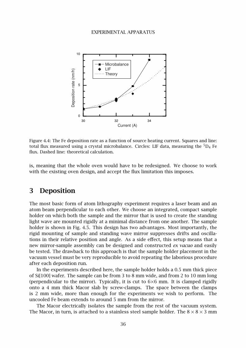
EXPERIMENTAL APPARATUS
30 32 34
0
5
10
Microbalance LIF Theory
Depositio
n r
ate
(nm
/h)
Current (A)
Figure 4.4: The Fe deposition rate as a function of source heating current. Squares and line:
total flux measured using a crystal microbalance. Circles: LIF data, measuring the 5D4 Fe
flux. Dashed line: theoretical calculation.
is, meaning that the whole oven would have to be redesigned. We choose to work
with the existing oven design, and accept the flux limitation this imposes.
3 Deposition
The most basic form of atom lithography experiment requires a laser beam and an
atom beam perpendicular to each other. We choose an integrated, compact sample
holder on which both the sample and the mirror that is used to create the standing
light wave are mounted rigidly at a minimal distance from one another. The sample
holder is shown in Fig. 4.5. This design has two advantages. Most importantly, the
rigid mounting of sample and standing wave mirror suppresses drifts and oscilla-
tions in their relative position and angle. As a side effect, this setup means that a
new mirror-sample assembly can be designed and constructed ex vacuo and easily
be tested. The drawback to this approach is that the sample holder placement in the
vacuum vessel must be very reproducible to avoid repeating the laborious procedure
after each deposition run.
In the experiments described here, the sample holder holds a 0.5 mm thick piece
of Si[100] wafer. The sample can be from 3 to 8 mm wide, and from 2 to 10 mm long
(perpendicular to the mirror). Typically, it is cut to 6×6 mm. It is clamped rigidly
onto a 4 mm thick Macor slab by screw-clamps. The space between the clamps
is 2 mm wide, more than enough for the experiments we wish to perform. The
uncooled Fe beam extends to around 5 mm from the mirror.
The Macor electrically isolates the sample from the rest of the vacuum system.
The Macor, in turn, is attached to a stainless steel sample holder. The 8× 8× 3 mm
36
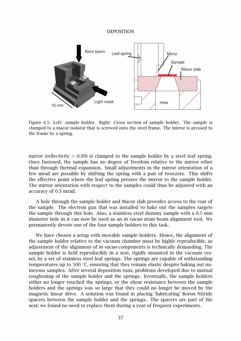
DEPOSITION
Atom beam
Light mask
Leaf spring
Sample
Macor slab
Mirror
Hole16 mm
Figure 4.5: Left: sample holder. Right: Cross section of sample holder. The sample is
clamped to a macor isolator that is screwed onto the steel frame. The mirror is pressed to
the frame by a spring.
mirror (reflectivity > 0.99) is clamped to the sample holder by a steel leaf spring.
Once fastened, the sample has no degree of freedom relative to the mirror other
than through thermal expansion. Small adjustments in the mirror orientation of a
few mrad are possible by shifting the spring with a pair of tweezers. This shifts
the effective point where the leaf spring presses the mirror to the sample holder.
The mirror orientation with respect to the samples could thus be adjusted with an
accuracy of 0.5 mrad.
A hole through the sample holder and Macor slab provides access to the rear of
the sample. The electron gun that was installed to bake out the samples targets
the sample through this hole. Also, a stainless steel dummy sample with a 0.5 mm
diameter hole in it can now be used as an in vacuo atom beam alignment tool. We
permanently devote one of the four sample holders to this task.
We have chosen a setup with movable sample holders. Hence, the alignment of
the sample holder relative to the vacuum chamber must be highly reproducible, as
adjustment of the alignment of in vacuo components is technically demanding. The
sample holder is held reproducibly in a seat, rigidly mounted in the vacuum ves-
sel, by a set of stainless steel leaf springs. The springs are capable of withstanding
temperatures up to 500 C, ensuring that they remain elastic despite baking out nu-
merous samples. After several deposition runs, problems developed due to mutual
roughening of the sample holder and the springs. Eventually, the sample holders
either no longer touched the springs, or the shear resistance between the sample
holders and the springs was so large that they could no longer be moved by the
magnetic linear drive. A solution was found in placing ’lubricating’ Boron Nitride
spacers between the sample holder and the springs. The spacers are part of the
seat; we found no need to replace them during a year of frequent experiments.
37
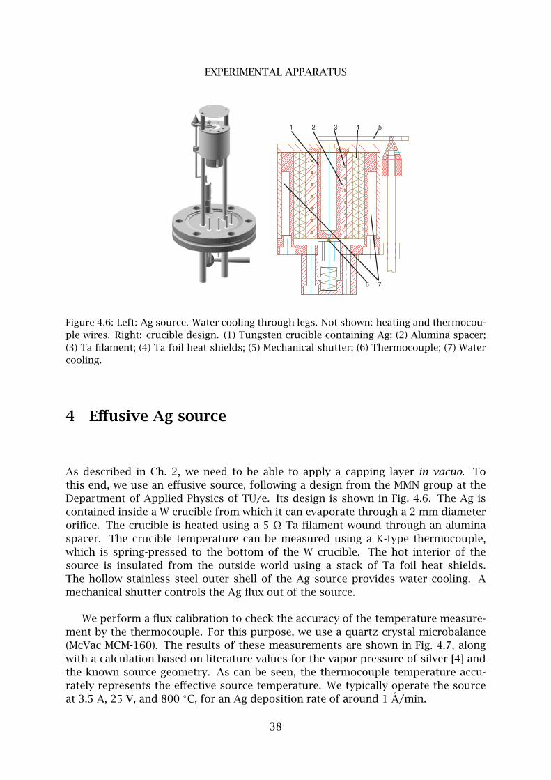
EXPERIMENTAL APPARATUS
1 2 3 4 5
6 7
Figure 4.6: Left: Ag source. Water cooling through legs. Not shown: heating and thermocou-
ple wires. Right: crucible design. (1) Tungsten crucible containing Ag; (2) Alumina spacer;
(3) Ta filament; (4) Ta foil heat shields; (5) Mechanical shutter; (6) Thermocouple; (7) Water
cooling.
4 Effusive Ag source
As described in Ch. 2, we need to be able to apply a capping layer in vacuo. To
this end, we use an effusive source, following a design from the MMN group at the
Department of Applied Physics of TU/e. Its design is shown in Fig. 4.6. The Ag is
contained inside a W crucible from which it can evaporate through a 2 mm diameter
orifice. The crucible is heated using a 5 Ω Ta filament wound through an alumina
spacer. The crucible temperature can be measured using a K-type thermocouple,
which is spring-pressed to the bottom of the W crucible. The hot interior of the
source is insulated from the outside world using a stack of Ta foil heat shields.
The hollow stainless steel outer shell of the Ag source provides water cooling. A
mechanical shutter controls the Ag flux out of the source.
We perform a flux calibration to check the accuracy of the temperature measure-
ment by the thermocouple. For this purpose, we use a quartz crystal microbalance
(McVac MCM-160). The results of these measurements are shown in Fig. 4.7, along
with a calculation based on literature values for the vapor pressure of silver [4] and
the known source geometry. As can be seen, the thermocouple temperature accu-
rately represents the effective source temperature. We typically operate the source
at 3.5 A, 25 V, and 800 C, for an Ag deposition rate of around 1 A/min.
38
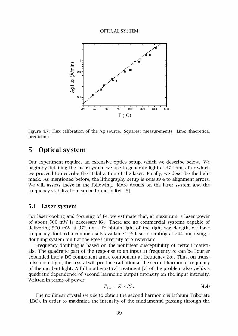
OPTICAL SYSTEM
720 740 760 780 800 820 840 860
0.1
0.5
1
Ag
flux
(Å/m
in)
T (°C)
Figure 4.7: Flux calibration of the Ag source. Squares: measurements. Line: theoretical
prediction.
5 Optical system
Our experiment requires an extensive optics setup, which we describe below. We
begin by detailing the laser system we use to generate light at 372 nm, after which
we proceed to describe the stabilization of the laser. Finally, we describe the light
mask. As mentioned before, the lithography setup is sensitive to alignment errors.
We will assess these in the following. More details on the laser system and the
frequency stabilization can be found in Ref. [5].
5.1 Laser system
For laser cooling and focusing of Fe, we estimate that, at maximum, a laser power
of about 500 mW is necessary [6]. There are no commercial systems capable of
delivering 500 mW at 372 nm. To obtain light of the right wavelength, we have
frequency doubled a commercially available Ti:S laser operating at 744 nm, using a
doubling system built at the Free University of Amsterdam.
Frequency doubling is based on the nonlinear susceptibility of certain materi-
als. The quadratic part of the response to an input at frequency ω can be Fourier
expanded into a DC component and a component at frequency 2ω. Thus, on trans-
mission of light, the crystal will produce radiation at the second harmonic frequency
of the incident light. A full mathematical treatment [7] of the problem also yields a
quadratic dependence of second harmonic output intensity on the input intensity.
Written in terms of power:
P2ω = K × P2ω. (4.4)
The nonlinear crystal we use to obtain the second harmonic is Lithium Triborate
(LBO). In order to maximize the intensity of the fundamental passing through the
39
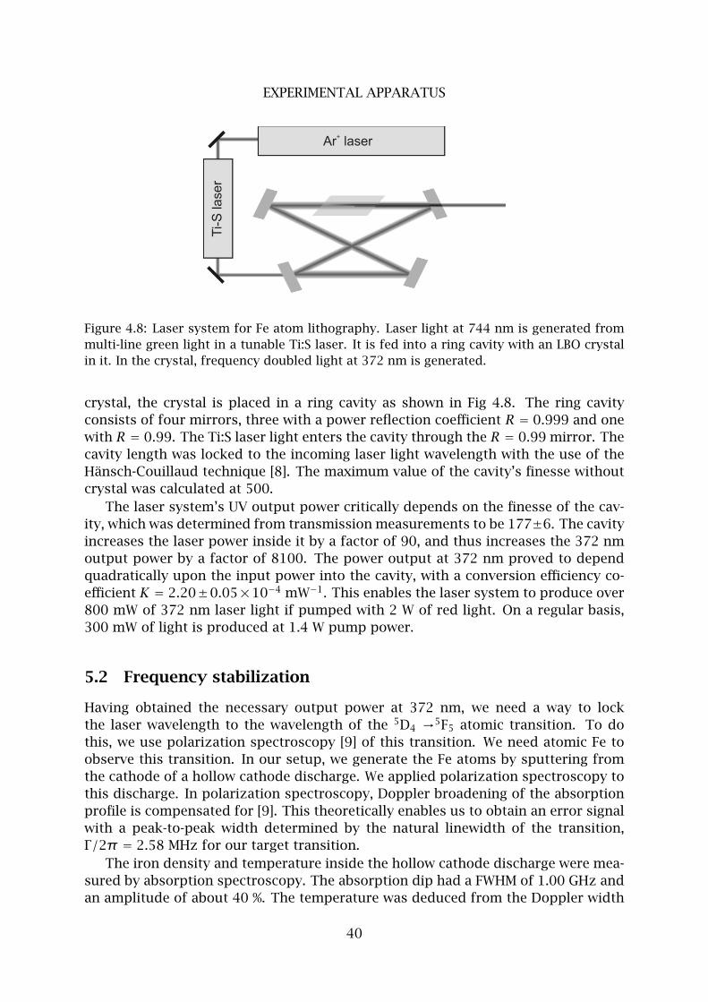
EXPERIMENTAL APPARATUS
Figure 4.8: Laser system for Fe atom lithography. Laser light at 744 nm is generated from
multi-line green light in a tunable Ti:S laser. It is fed into a ring cavity with an LBO crystal
in it. In the crystal, frequency doubled light at 372 nm is generated.
crystal, the crystal is placed in a ring cavity as shown in Fig 4.8. The ring cavity
consists of four mirrors, three with a power reflection coefficient R = 0.999 and one
with R = 0.99. The Ti:S laser light enters the cavity through the R = 0.99 mirror. The
cavity length was locked to the incoming laser light wavelength with the use of the
Hansch-Couillaud technique [8]. The maximum value of the cavity’s finesse without
crystal was calculated at 500.
The laser system’s UV output power critically depends on the finesse of the cav-
ity, which was determined from transmission measurements to be 177±6. The cavity
increases the laser power inside it by a factor of 90, and thus increases the 372 nm
output power by a factor of 8100. The power output at 372 nm proved to depend
quadratically upon the input power into the cavity, with a conversion efficiency co-
efficient K = 2.20±0.05×10⁻⁴ mW−1. This enables the laser system to produce over
800 mW of 372 nm laser light if pumped with 2 W of red light. On a regular basis,
300 mW of light is produced at 1.4 W pump power.
5.2 Frequency stabilization
Having obtained the necessary output power at 372 nm, we need a way to lock
the laser wavelength to the wavelength of the 5D4 →5F5 atomic transition. To do
this, we use polarization spectroscopy [9] of this transition. We need atomic Fe to
observe this transition. In our setup, we generate the Fe atoms by sputtering from
the cathode of a hollow cathode discharge. We applied polarization spectroscopy to
this discharge. In polarization spectroscopy, Doppler broadening of the absorption
profile is compensated for [9]. This theoretically enables us to obtain an error signal
with a peak-to-peak width determined by the natural linewidth of the transition,
Γ/2π = 2.58 MHz for our target transition.
The iron density and temperature inside the hollow cathode discharge were mea-
sured by absorption spectroscopy. The absorption dip had a FWHM of 1.00 GHz and
an amplitude of about 40 %. The temperature was deduced from the Doppler width
40
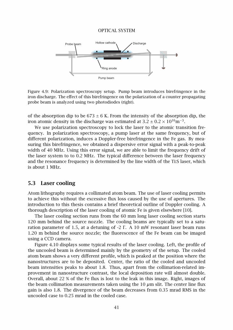
OPTICAL SYSTEM
Figure 4.9: Polarization spectroscopy setup. Pump beam introduces birefringence in the
iron discharge. The effect of this birefringence on the polarization of a counter propagating
probe beam is analyzed using two photodiodes (right).
of the absorption dip to be 673± 6 K. From the intensity of the absorption dip, the
iron atomic density in the discharge was estimated at 3.2± 0.2× 10¹⁶m−3.
We use polarization spectroscopy to lock the laser to the atomic transition fre-
quency. In polarization spectroscopy, a pump laser at the same frequency, but of
different polarization, induces a Doppler-free birefringence in the Fe gas. By mea-
suring this birefringence, we obtained a dispersive error signal with a peak-to-peak
width of 40 MHz. Using this error signal, we are able to limit the frequency drift of
the laser system to to 0.2 MHz. The typical difference between the laser frequency
and the resonance frequency is determined by the line width of the Ti:S laser, which
is about 1 MHz.
5.3 Laser cooling
Atom lithography requires a collimated atom beam. The use of laser cooling permits
to achieve this without the excessive flux loss caused by the use of apertures. The
introduction to this thesis contains a brief theoretical outline of Doppler cooling. A
thorough description of the laser cooling of atomic Fe is given elsewhere [10].
The laser cooling section runs from the 60 mm long laser cooling section starts
120 mm behind the source nozzle. The cooling beams are typically set to a satu-
ration parameter of 1.5, at a detuning of -2 Γ . A 10 mW resonant laser beam runs
1.20 m behind the source nozzle; the fluorescence of the Fe beam can be imaged
using a CCD camera.
Figure 4.10 displays some typical results of the laser cooling. Left, the profile of
the uncooled beam is determined mainly by the geometry of the setup. The cooled
atom beam shows a very different profile, which is peaked at the position where the
nanostructures are to be deposited. Center, the ratio of the cooled and uncooled
beam intensities peaks to about 1.8. Thus, apart from the collimation-related im-
provement in nanostructure contrast, the local deposition rate will almost double.
Overall, about 22 % of the Fe flux is lost to the leak in this image. Right, images of
the beam collimation measurements taken using the 10 µm slit. The center line flux
gain is also 1.8. The divergence of the beam decreases from 0.35 mrad RMS in the
uncooled case to 0.25 mrad in the cooled case.
41
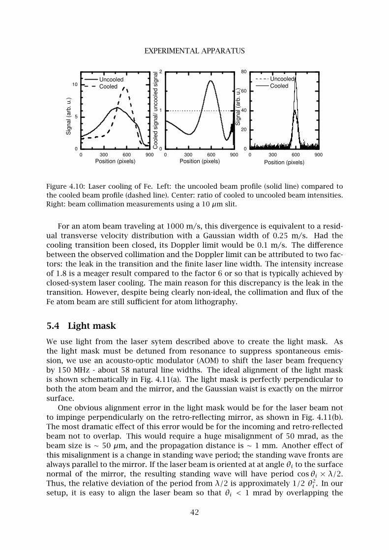
EXPERIMENTAL APPARATUS
0 300 600 9000
1
2
0 300 600 9000
20
40
60
80
0 300 600 9000
5
10
S
igna
l (ar
b. u
.)
Position (pixels)
Uncooled Cooled
Coo
led
sign
al/ u
ncoo
led
sign
alPosition (pixels)
Sig
nal (
arb.
u.)
Position (pixels)
Uncooled Cooled
Figure 4.10: Laser cooling of Fe. Left: the uncooled beam profile (solid line) compared to
the cooled beam profile (dashed line). Center: ratio of cooled to uncooled beam intensities.
Right: beam collimation measurements using a 10 µm slit.
For an atom beam traveling at 1000 m/s, this divergence is equivalent to a resid-
ual transverse velocity distribution with a Gaussian width of 0.25 m/s. Had the
cooling transition been closed, its Doppler limit would be 0.1 m/s. The difference
between the observed collimation and the Doppler limit can be attributed to two fac-
tors: the leak in the transition and the finite laser line width. The intensity increase
of 1.8 is a meager result compared to the factor 6 or so that is typically achieved by
closed-system laser cooling. The main reason for this discrepancy is the leak in the
transition. However, despite being clearly non-ideal, the collimation and flux of the
Fe atom beam are still sufficient for atom lithography.
5.4 Light mask
We use light from the laser sytem described above to create the light mask. As
the light mask must be detuned from resonance to suppress spontaneous emis-
sion, we use an acousto-optic modulator (AOM) to shift the laser beam frequency
by 150 MHz - about 58 natural line widths. The ideal alignment of the light mask
is shown schematically in Fig. 4.11(a). The light mask is perfectly perpendicular to
both the atom beam and the mirror, and the Gaussian waist is exactly on the mirror
surface.
One obvious alignment error in the light mask would be for the laser beam not
to impinge perpendicularly on the retro-reflecting mirror, as shown in Fig. 4.11(b).
The most dramatic effect of this error would be for the incoming and retro-reflected
beam not to overlap. This would require a huge misalignment of 50 mrad, as the
beam size is ∼ 50 µm, and the propagation distance is ∼ 1 mm. Another effect of
this misalignment is a change in standing wave period; the standing wave fronts are
always parallel to the mirror. If the laser beam is oriented at at angle θi to the surface
normal of the mirror, the resulting standing wave will have period cosθi × λ/2.
Thus, the relative deviation of the period from λ/2 is approximately 1/2 θ2i . In our
setup, it is easy to align the laser beam so that θi < 1 mrad by overlapping the
42
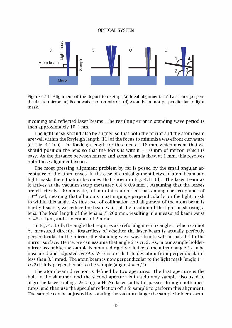
OPTICAL SYSTEM
Figure 4.11: Alignment of the deposition setup. (a) Ideal alignment. (b) Laser not perpen-
dicular to mirror. (c) Beam waist not on mirror. (d) Atom beam not perpendicular to light
mask.
incoming and reflected laser beams. The resulting error in standing wave period is
then approximately 10−4 nm.
The light mask should also be aligned so that both the mirror and the atom beam
are well within the Rayleigh length [11] of the focus to minimize wavefront curvature
(cf. Fig. 4.11(c)). The Rayleigh length for this focus is 16 mm, which means that we
should position the lens so that the focus is within ± 10 mm of mirror, which is
easy. As the distance between mirror and atom beam is fixed at 1 mm, this resolves
both these alignment issues.
The most pressing alignment problem by far is posed by the small angular ac-
ceptance of the atom lenses. In the case of a misalignment between atom beam and
light mask, the situation becomes that shown in Fig. 4.11 (d). The laser beam as
it arrives at the vacuum setup measured 0.8 × 0.9 mm2. Assuming that the lenses
are effectively 100 nm wide, a 1 mm thick atom lens has an angular acceptance of
10−4 rad, meaning that all atoms must impinge perpendicularly on the light mask
to within this angle. As this level of collimation and alignment of the atom beam is
hardly feasible, we reduce the beam waist at the location of the light mask using a
lens. The focal length of the lens is f=200 mm, resulting in a measured beam waist
of 45± 1µm, and a tolerance of 2 mrad.
In Fig. 4.11 (d), the angle that requires a careful alignment is angle 1, which cannot
be measured directly. Regardless of whether the laser beam is actually perfectly
perpendicular to the mirror, the standing wave wave fronts will be parallel to the
mirror surface. Hence, we can assume that angle 2 is π/2. As, in our sample holder-
mirror assembly, the sample is mounted rigidly relative to the mirror, angle 3 can be
measured and adjusted ex situ. We ensure that its deviation from perpendicular is
less than 0.5 mrad. The atom beam is now perpendicular to the light mask (angle 1 =π/2) if it is perpendicular to the sample (angle 4 = π/2).
The atom beam direction is defined by two apertures. The first aperture is the
hole in the skimmer, and the second aperture is in a dummy sample also used to
align the laser cooling. We align a He:Ne laser so that it passes through both aper-
tures, and then use the specular reflection off a Si sample to perform this alignment.
The sample can be adjusted by rotating the vacuum flange the sample holder assem-
43

EXPERIMENTAL APPARATUS
bly is attached to - the angle between the sample and the atom beam in the other
direction is not critical. The remaining aberration from perpendicular of angle 4 is
estimated around 0.3 mrad. This can only be done if the entire vacuum is brought
up to atmosphere. However, repeated sample exchanges showed that the alignment
of the standing light wave is preserved from sample to sample to within 0.3 mrad.
This means that the alignment procedure does not have to be repeated between
depositions.
6 Conclusion
In conclusion, we have constructed and tested a setup for atom lithography of Fe.
This setup allows for atom lithography in a clean environment, corrosion protection
of the atom lithography setup, and a relatively high production rate of several sam-
ples per day. It can also be used to investigate the influence of substrate conditions
on the diffusion and growth of the nanostructures. Adapting the light mask geome-
try only requires changing the sample holder. This is a unique versatility that is not
seen in other atom lithography setups.
Adapting the setup to fit other materials would not take a large amount of effort,
provided that the laser wavelength needed is not too far from that of Fe. In this case,
exchanging the crucible in the Fe source with one containing the desired element,
replacing the nonlinear crystal in the cavity, and using a different hollow cathode
for the frequency stabilization suffices.
References
[1] T. I. Gombosi, Gaskinetic theory (Cambridge University Press, Cambridge, 1994)
[2] R. C. M. Bosch, H. C. W. Beijerinck, P. van der Straten, and K. A. H. van Leeuwen, Eur.
Phys. J. A. P. 18, 221-227 (2002)
[3] H.Metcalf and P. van der Straten, it Laser Cooling and Trapping (Springer Verlag, Hei-
delberg, 1999).
[4] A. N. Nesmeyanov, Vapor pressure of the chemical elements, Elsevier (1963)
[5] B. Smeets, R. C. M. Bosch, P. van der Straten, E. te Sligte, R. E. Scholten, H. C. W. Beijer-
inck, and K. A. H. van Leeuwen, Appl. Phys. B, 76, 815-819 (2003)
[6] R. C. M. Bosch, PhD thesis, TU/e (2002)
[7] Y. R. Shen, The Principles of Nonlinear Optics, J. Wiley (1984)
[8] T. W. Hansch and B. Couillaud, Opt. Comm. 35, 441-444 (1980)
[9] W. Demtroder, Laser Spectroscopy, Basic Concepts and Instrumentation, Springer-
Verlag (1981)
44
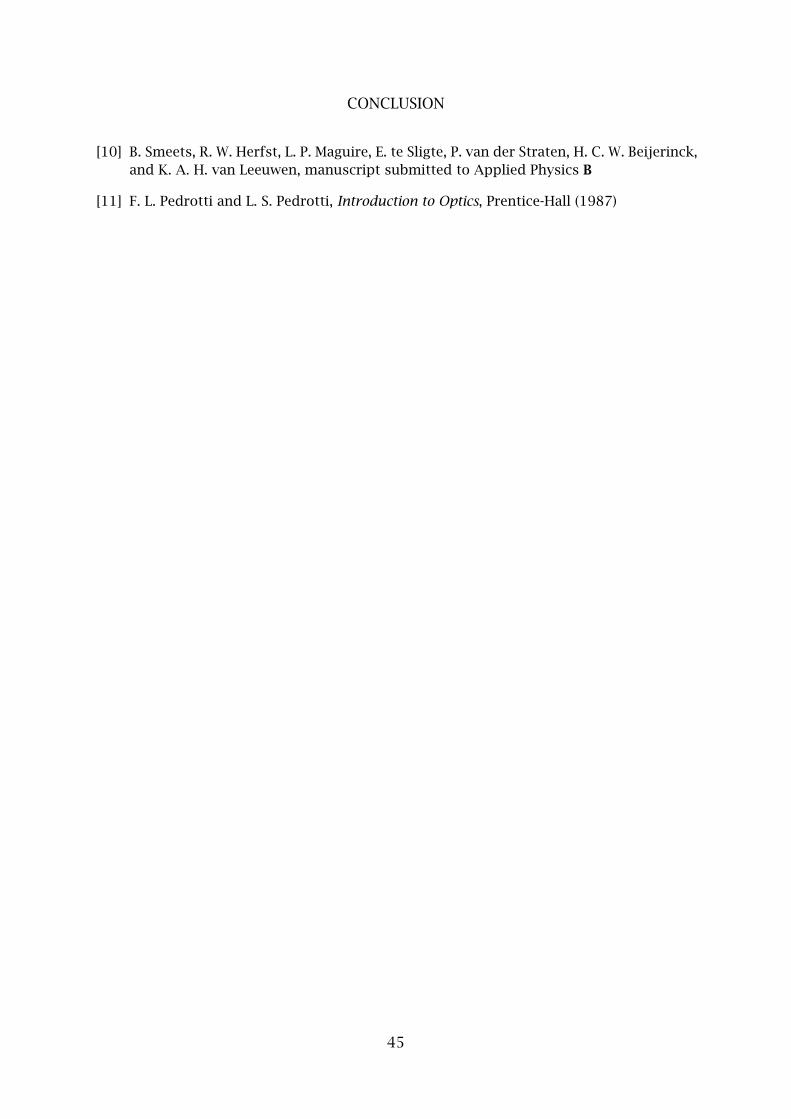
CONCLUSION
[10] B. Smeets, R. W. Herfst, L. P. Maguire, E. te Sligte, P. van der Straten, H. C. W. Beijerinck,
and K. A. H. van Leeuwen, manuscript submitted to Applied Physics B
[11] F. L. Pedrotti and L. S. Pedrotti, Introduction to Optics, Prentice-Hall (1987)
45

EXPERIMENTAL APPARATUS
46
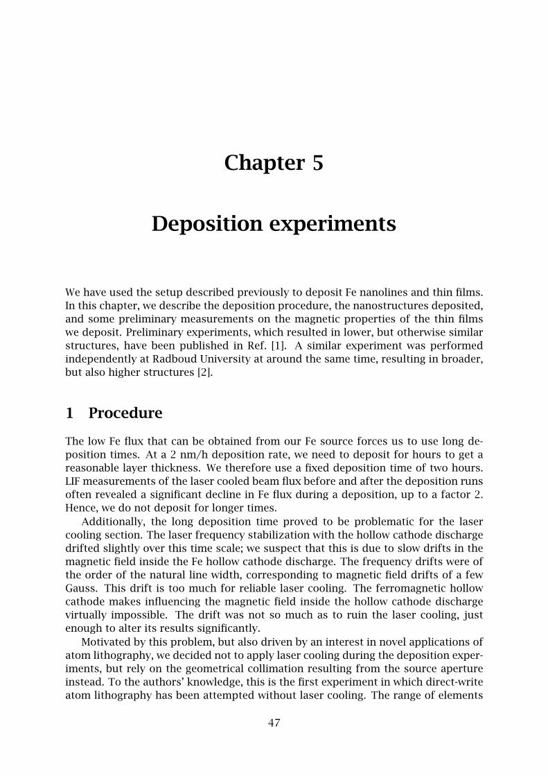
Chapter 5
Deposition experiments
We have used the setup described previously to deposit Fe nanolines and thin films.
In this chapter, we describe the deposition procedure, the nanostructures deposited,
and some preliminary measurements on the magnetic properties of the thin films
we deposit. Preliminary experiments, which resulted in lower, but otherwise similar
structures, have been published in Ref. [1]. A similar experiment was performed
independently at Radboud University at around the same time, resulting in broader,
but also higher structures [2].
1 Procedure
The low Fe flux that can be obtained from our Fe source forces us to use long de-
position times. At a 2 nm/h deposition rate, we need to deposit for hours to get a
reasonable layer thickness. We therefore use a fixed deposition time of two hours.
LIF measurements of the laser cooled beam flux before and after the deposition runs
often revealed a significant decline in Fe flux during a deposition, up to a factor 2.
Hence, we do not deposit for longer times.
Additionally, the long deposition time proved to be problematic for the laser
cooling section. The laser frequency stabilization with the hollow cathode discharge
drifted slightly over this time scale; we suspect that this is due to slow drifts in the
magnetic field inside the Fe hollow cathode discharge. The frequency drifts were of
the order of the natural line width, corresponding to magnetic field drifts of a few
Gauss. This drift is too much for reliable laser cooling. The ferromagnetic hollow
cathode makes influencing the magnetic field inside the hollow cathode discharge
virtually impossible. The drift was not so much as to ruin the laser cooling, just
enough to alter its results significantly.
Motivated by this problem, but also driven by an interest in novel applications of
atom lithography, we decided not to apply laser cooling during the deposition exper-
iments, but rely on the geometrical collimation resulting from the source aperture
instead. To the authors’ knowledge, this is the first experiment in which direct-write
atom lithography has been attempted without laser cooling. The range of elements
47
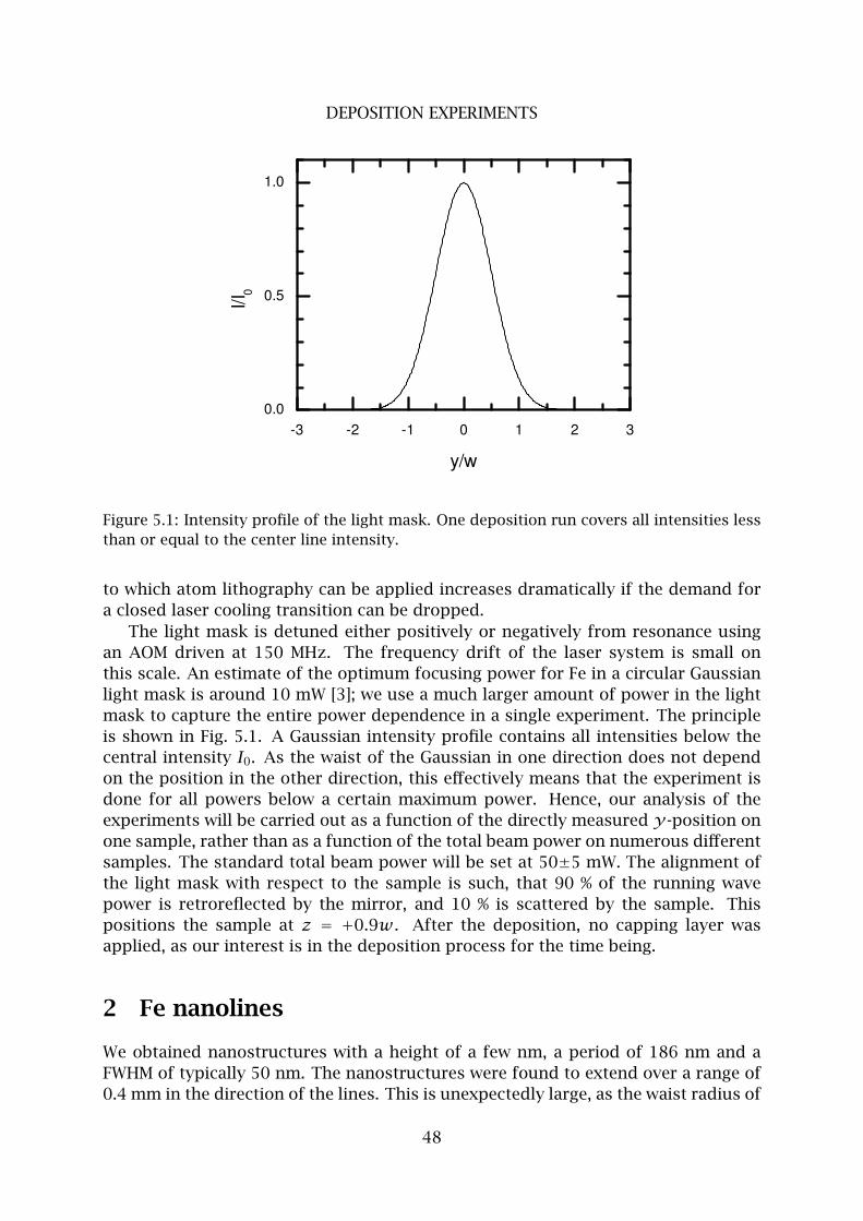
DEPOSITION EXPERIMENTS
-3 -2 -1 0 1 2 30.0
0.5
1.0
I/I0
y/w
Figure 5.1: Intensity profile of the light mask. One deposition run covers all intensities less
than or equal to the center line intensity.
to which atom lithography can be applied increases dramatically if the demand for
a closed laser cooling transition can be dropped.
The light mask is detuned either positively or negatively from resonance using
an AOM driven at 150 MHz. The frequency drift of the laser system is small on
this scale. An estimate of the optimum focusing power for Fe in a circular Gaussian
light mask is around 10 mW [3]; we use a much larger amount of power in the light
mask to capture the entire power dependence in a single experiment. The principle
is shown in Fig. 5.1. A Gaussian intensity profile contains all intensities below the
central intensity I0. As the waist of the Gaussian in one direction does not depend
on the position in the other direction, this effectively means that the experiment is
done for all powers below a certain maximum power. Hence, our analysis of the
experiments will be carried out as a function of the directly measured y-position on
one sample, rather than as a function of the total beam power on numerous different
samples. The standard total beam power will be set at 50±5 mW. The alignment of
the light mask with respect to the sample is such, that 90 % of the running wave
power is retroreflected by the mirror, and 10 % is scattered by the sample. This
positions the sample at z = +0.9w. After the deposition, no capping layer was
applied, as our interest is in the deposition process for the time being.
2 Fe nanolines
We obtained nanostructures with a height of a few nm, a period of 186 nm and a
FWHM of typically 50 nm. The nanostructures were found to extend over a range of
0.4 mm in the direction of the lines. This is unexpectedly large, as the waist radius of
48
FE NANOLINES
0 1000 2000 3000 4000 5000
0
500
1000
1500
2000
2500z (nm)
x (nm)
y (n
m)
0
1.000
2.000
3.000
4.000
Figure 5.2: AFM scan of Fe nanolines deposited by atom lithography.
the light mask was only 0.05 mm. An Atomic Force Microscope (AFM) scan of some
of these structures is shown in Fig. 5.2. The highly periodic nature of the structures
is immediately apparent. The slight wavering of the lines is most likely due to drifts
of the AFM piezos, as the same sample area looks slightly different for every scan.
We quantify the properties of the nanostructures by averaging ten lines of an AFM
scan. This yields a structure profile as shown in Fig. 5.3. The data are represented
by squares, and the drawn line represents a Gaussian fit. The width and height of all
nanostructures discussed in this thesis have been extracted from similar Gauss fits.
The asymmetry that is apparent in the peak shape is possibly an artifact caused by
e.g., the shape of the AFM tip, or the AFM electronics. It could also be caused by an
effect in the deposition process, such as a misalignment.
Curiously, we initially measured a period that differed significantly from the nom-
inal value of 186.05 nm, initially by over 20 %. To decide whether something was
wrong in the deposition process or in the AFM calibration, we used a sample that
had been treated atom lithographically with He* at the Free University of Amster-
dam [8]. The nominal period of these structures is 541.5 nm, half the wavelength of
the 1083 nm transition used in the experiment. The ratio of the two periods is 2.91;
with the AFM, we measured 2.87 ± 0.06. This excellent agreement was used for a
re-calibration of the AFM. For all further scans, we used the measured nanostructure
period as a length scale, which was set at 186 nm.
Scanning over y , we obtain an image of the power dependence of the charac-
teristics of the lines, and hence the deposition process. For positive detuning, this
measurement is shown in Fig. 5.4. The width of the lines is shown on the left; the full
width at half maximum (FWHM) of the nanolines is around 50 nm for all locations
where the nanolines can be clearly discerned. The height of the nanolines (on the
right) increases towards the center of the profile.
Similar measurements were performed for negative detuning. Due to a disap-
pointing overall Fe flux, these experiments have not yet yielded satisfactory data for
a proper analysis. However, it did become clear that the nanolines deposited at neg-
49
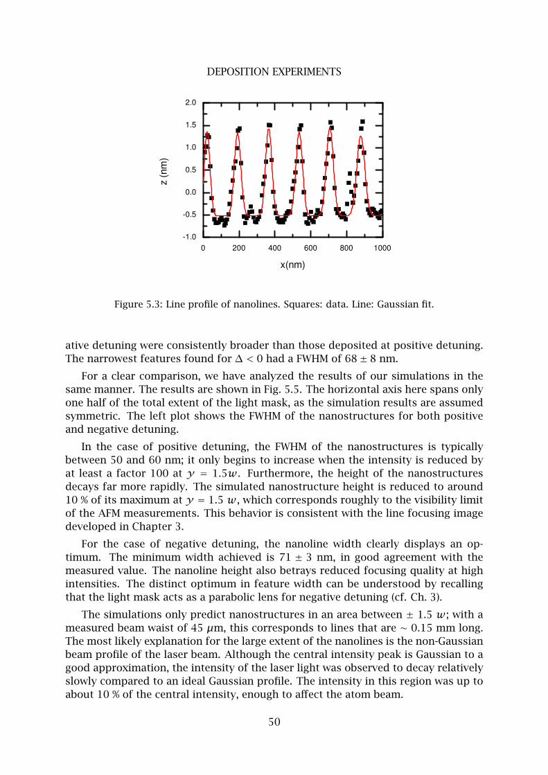
DEPOSITION EXPERIMENTS
0 200 400 600 800 1000-1.0
-0.5
0.0
0.5
1.0
1.5
2.0
z (n
m)
x(nm)
Figure 5.3: Line profile of nanolines. Squares: data. Line: Gaussian fit.
ative detuning were consistently broader than those deposited at positive detuning.
The narrowest features found for ∆ < 0 had a FWHM of 68± 8 nm.
For a clear comparison, we have analyzed the results of our simulations in the
same manner. The results are shown in Fig. 5.5. The horizontal axis here spans only
one half of the total extent of the light mask, as the simulation results are assumed
symmetric. The left plot shows the FWHM of the nanostructures for both positive
and negative detuning.
In the case of positive detuning, the FWHM of the nanostructures is typically
between 50 and 60 nm; it only begins to increase when the intensity is reduced by
at least a factor 100 at y = 1.5w. Furthermore, the height of the nanostructures
decays far more rapidly. The simulated nanostructure height is reduced to around
10 % of its maximum at y = 1.5 w, which corresponds roughly to the visibility limit
of the AFM measurements. This behavior is consistent with the line focusing image
developed in Chapter 3.
For the case of negative detuning, the nanoline width clearly displays an op-
timum. The minimum width achieved is 71 ± 3 nm, in good agreement with the
measured value. The nanoline height also betrays reduced focusing quality at high
intensities. The distinct optimum in feature width can be understood by recalling
that the light mask acts as a parabolic lens for negative detuning (cf. Ch. 3).
The simulations only predict nanostructures in an area between ± 1.5 w; with a
measured beam waist of 45 µm, this corresponds to lines that are ∼ 0.15 mm long.
The most likely explanation for the large extent of the nanolines is the non-Gaussian
beam profile of the laser beam. Although the central intensity peak is Gaussian to a
good approximation, the intensity of the laser light was observed to decay relatively
slowly compared to an ideal Gaussian profile. The intensity in this region was up to
about 10 % of the central intensity, enough to affect the atom beam.
50
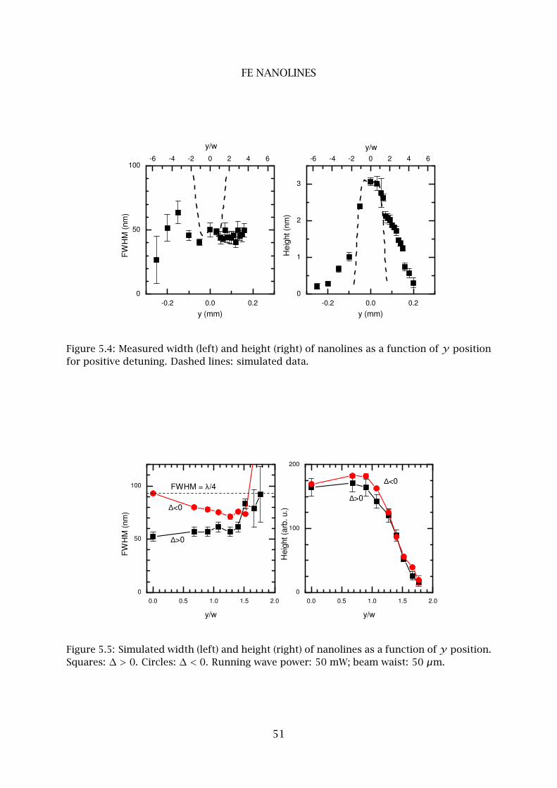
FE NANOLINES
-0.2 0.0 0.20
50
100
-0.2 0.0 0.20
1
2
3
-6 -4 -2 0 2 4 6-6 -4 -2 0 2 4 6
FW
HM
(nm
)
y (mm)
Hei
ght (
nm)
y (mm)
y/w y/w
Figure 5.4: Measured width (left) and height (right) of nanolines as a function of y position
for positive detuning. Dashed lines: simulated data.
0.0 0.5 1.0 1.5 2.00
50
100
0.0 0.5 1.0 1.5 2.00
100
200
FWHM = λ/4
∆<0
∆>0
FW
HM
(nm
)
y/w
∆>0
∆<0
Hei
ght (
arb.
u.)
y/w
Figure 5.5: Simulated width (left) and height (right) of nanolines as a function of y position.
Squares: ∆ > 0. Circles: ∆ < 0. Running wave power: 50 mW; beam waist: 50 µm.
51
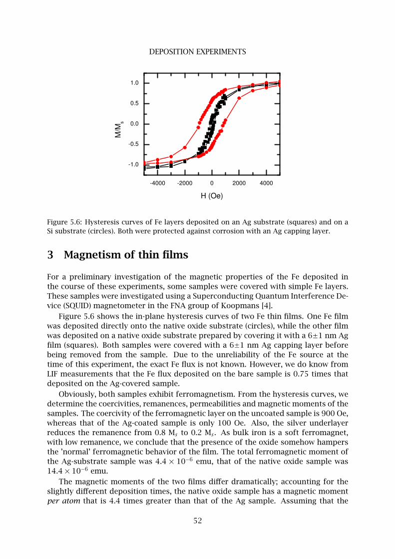
DEPOSITION EXPERIMENTS
-4000 -2000 0 2000 4000
-1.0
-0.5
0.0
0.5
1.0
M/M
s
H (Oe)
Figure 5.6: Hysteresis curves of Fe layers deposited on an Ag substrate (squares) and on a
Si substrate (circles). Both were protected against corrosion with an Ag capping layer.
3 Magnetism of thin films
For a preliminary investigation of the magnetic properties of the Fe deposited in
the course of these experiments, some samples were covered with simple Fe layers.
These samples were investigated using a Superconducting Quantum Interference De-
vice (SQUID) magnetometer in the FNA group of Koopmans [4].
Figure 5.6 shows the in-plane hysteresis curves of two Fe thin films. One Fe film
was deposited directly onto the native oxide substrate (circles), while the other film
was deposited on a native oxide substrate prepared by covering it with a 6±1 nm Ag
film (squares). Both samples were covered with a 6±1 nm Ag capping layer before
being removed from the sample. Due to the unreliability of the Fe source at the
time of this experiment, the exact Fe flux is not known. However, we do know from
LIF measurements that the Fe flux deposited on the bare sample is 0.75 times that
deposited on the Ag-covered sample.
Obviously, both samples exhibit ferromagnetism. From the hysteresis curves, we
determine the coercivities, remanences, permeabilities and magnetic moments of the
samples. The coercivity of the ferromagnetic layer on the uncoated sample is 900 Oe,
whereas that of the Ag-coated sample is only 100 Oe. Also, the silver underlayer
reduces the remanence from 0.8 Ms to 0.2 Ms . As bulk iron is a soft ferromagnet,
with low remanence, we conclude that the presence of the oxide somehow hampers
the ’normal’ ferromagnetic behavior of the film. The total ferromagnetic moment of
the Ag-substrate sample was 4.4 × 10⁻⁶ emu, that of the native oxide sample was
14.4× 10⁻⁶ emu.
The magnetic moments of the two films differ dramatically; accounting for the
slightly different deposition times, the native oxide sample has a magnetic moment
per atom that is 4.4 times greater than that of the Ag sample. Assuming that the
52
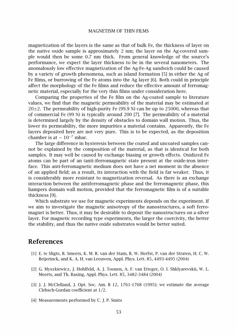
MAGNETISM OF THIN FILMS
magnetization of the layers is the same as that of bulk Fe, the thickness of layer on
the native oxide sample is approximately 2 nm; the layer on the Ag-covered sam-
ple would then be some 0.7 nm thick. From general knowledge of the source’s
performance, we expect the layer thickness to be in the several nanometers. The
anomalously low effective magnetization of the Ag-Fe-Ag sandwich could be caused
by a variety of growth phenomena, such as island formation [5] in either the Ag of
Fe films, or burrowing of the Fe atoms into the Ag layer [6]. Both could in principle
affect the morphology of the Fe films and reduce the effective amount of ferromag-
netic material, especially for the very thin films under consideration here.
Comparing the properties of the Fe film on the Ag-coated sample to literature
values, we find that the magnetic permeability of the material may be estimated at
20±2. The permeability of high-purity Fe (99.9 %) can be up to 25000, whereas that
of commercial Fe (99 %) is typically around 200 [7]. The permeability of a material
is determined largely by the density of obstacles to domain wall motion. Thus, the
lower its permeability, the more impurities a material contains. Apparently, the Fe
layers deposited here are not very pure. This is to be expected, as the deposition
chamber is at ∼ 10−7 mbar.
The large difference in hysteresis between the coated and uncoated samples can-
not be explained by the composition of the material, as that is identical for both
samples. It may well be caused by exchange biasing or growth effects. Oxidized Fe
atoms can be part of an (anti-)ferromagnetic state present at the oxide-iron inter-
face. This anti-ferromagnetic medium does not have a net moment in the absence
of an applied field; as a result, its interaction with the field is far weaker. Thus, it
is considerably more resistant to magnetization reversal. As there is an exchange
interaction between the antiferromagnetic phase and the ferromagnetic phase, this
hampers domain wall motion, provided that the ferromagnetic film is of a suitable
thickness [9].
Which substrate we use for magnetic experiments depends on the experiment. If
we aim to investigate the magnetic anisotropy of the nanostructures, a soft ferro-
magnet is better. Thus, it may be desirable to deposit the nanostructures on a silver
layer. For magnetic recording type experiments, the larger the coercivity, the better
the stability, and thus the native oxide substrates would be better suited.
References
[1] E. te Sligte, B. Smeets, K. M. R. van der Stam, R. W. Herfst, P. van der Straten, H. C. W.
Beijerinck, and K. A. H. van Leeuwen, Appl. Phys. Lett. 85, 4493-4495 (2004)
[2] G. Myszkiewicz, J. Hohlfeld, A. J. Toonen, A. F. van Etteger, O. I. Shklyarevskii, W. L.
Meerts, and Th. Rasing, Appl. Phys. Lett. 85, 3482-3484 (2004)
[3] J. J. McClelland, J. Opt. Soc. Am. B 12, 1761-1768 (1995); we estimate the average
Clebsch-Gordan coefficient at 1/2.
[4] Measurements performed by C. J. P. Smits
53
DEPOSITION EXPERIMENTS
[5] J. Oster, M. Huth, L. Wiehl, and H. Adrian, J. Magn. Magn. Mater. 272-276, 1588-1589
(2004)
[6] D. E. Burgler, C. M. Schmidt, D. M. Schaller, F. Meisinger, R. Hofer, and H.-J. Guntherodt,
Phys. Rev. B 56 4149-4158 (1997)
[7] CRC Handbook of Chemistry and Physics, 79th Ed. (CRC Press, Boca Raton, 1998)
[8] Samples courtesy of W. Vassen
[9] J.-G. Hu, G.-J. Jin, and Y.-Q. Ma, J. Appl. Phys. 94, 2529-2533 (2003)
54

Chapter 6
Magnetism of periodic nanostructures
The reason for using Fe in our atom lithography experiment was the fact that it is
ferromagnetic. We therefore desire to investigate the magnetic properties of the
nanostructures we have deposited. In the last chapter, we have proven the ferro-
magnetic nature of the material we deposit. The next step is to find a signature of
the nanostructured nature of the deposited layer.
The simplest analysis technique available is the magneto-optical Kerr effect (MOKE),
which investigates the reflectivity of the magnetic material to discern signs of ferro-
magnetism [1]. Varying the applied magnetic field in both size and direction allows
for detection of magnetic anisotropy. This involves a laser, and its resolution is thus
limited by the spot size of the laser beam. Hence, the technique can only investigate
the properties of the nanostructured material averaged over many lines.
A large amount of theoretical [2] and experimental [3] work has been done on fer-
romagnetic nanowire arrays. However, most of this work concerns two-dimensional
arrays of nanowires which have been obtained by electrodepositing the metal in a
matrix. The results cannot be straightforwardly translated to the present work. A
better match is provided by one-dimensional arrays of nanowires made using elec-
tron beam lithography [4]. These are typically arrays of wires with a rectangular
cross-section, which are also different from the continuous modulated thin films we
investigate. We would be interested primarily in the effect of the modulation of the
surface shape of our thin film, which we expect to show up as an anisotropy in the
direction that is perpendicular to the nanolines and in the substrate plane.
This chapter will present some considerations on the magnetic anisotropy of
the ferromagnetic nanostructures produced in this thesis. To this end, we begin
by introducing the magnetic field generated by a magnetization distribution, also
known as the demagnetizing field. We describe the magnetostatic energy terms that
can play a role in the anisotropy of the nanostructures in section 2. The model we
use to investigate the anisotropy is introduced in section 3. The resulting stray fields
are presented in Sec. 4; the ensuing anisotropy is discussed in Sec. 5. We conclude
with a summary of further potential experiments.
55
MAGNETISM OF PERIODIC NANOSTRUCTURES
1 Demagnetizing field
A magnetized object will generate a magnetic field that normally extends outside
the object itself. This field is called the demagnetizing field, and it can be calculated
using Maxwell’s equations. These relations between electric field ~E, magnetic induc-
tion ~B, charge density ρ, and current density ~J can be found in any textbook [5, 6]
and read:∇ · ~E = ρ
ǫ0
∇× ~E = −∂~B∂t
∇ · ~B = 0
∇× ~B = µ0 ~J + µ0ǫ0∂ ~E∂t
(6.1)
By definition, the magnetization ~M is such, that:
~B = µ0( ~M + ~H). (6.2)
Inserting this into Maxwells equations, we get:
∇ · ~E = ρǫ0
∇× ~E = −µ0∂ ~H∂t− µ0
∂ ~M∂t
∇ · ~H = −∇ · ~M∇× ~H = ~J + ǫ0
∂ ~E∂t−∇× ~M
(6.3)
Now let us begin by noting that the magnetization enters into the right hand side
of these equations as a source term. Its divergence, for example, generates ~H just
as electric charge generates ~E. This is why we introduce a magnetic charge density
ρ∗ ≡ µ0∇ · ~M , and a magnetic current density ~J∗ ≡ µ0∂ ~M/∂t. The rotation of ~M
is effectively a bound current density, which can be removed from the equations
by separating the current density ~J into a magnetization-dependent part and a free
current density according to ~J = ~Jf + ~∇× ~M :
∇ · ~E = ρǫ0
∇× ~E = −µ0∂ ~H∂t− ~J∗
∇ · ~H = −ρ∗
µ0
∇× ~H = ~Jf + ǫ0∂ ~E∂t
(6.4)
The free current density is now the current density that results from the applied
currents in the system. We now have a set of equations that can be used to calculate~H for any given magnetization configuration. This will be very useful later on. As a
last remark, note that magnetic charge is every bit as conserved as electric charge,
and that its total in all space must necessarily be zero.
The preceding showed that magnetic charge generates ~H in exactly the same way
that electric charge generates ~E. Coulomb’s law in integral form states that:
~E(~r) = 1
4π
∫
~r − ~r ′|~r − ~r ′|3
ρ
ǫ0d3~r ′. (6.5)
56
ENERGY OF FERROMAGNETIC NANOSTRUCTURES
In the absence of free currents, the analogous formula for calculating ~H is:
~H(~r) = −1
4π
∫
~r − ~r ′|~r − ~r ′|3
ρ∗
µ0d3~r ′ ≡ ~Hd(~r). (6.6)
This field is called the demagnetizing field ~Hd. As it is generated only by the magne-
tization of an object, it is the only non-vanishing field when all external field sources
are removed. This is typically the field that a Magnetic Force Microscope (MFM) seeks
to detect [9].
2 Energy of ferromagnetic nanostructures
The energy of ferromagnetic nanostructures has several terms. We will first briefly
describe them, before going into the calculation of their contributions.
An external applied field obviously has an interaction with the magnetic nanos-
tructure, and this is by far the simplest of the energy terms under consideration
here. The applied field energy density is given by:
Ea = −µ0 ~Ha · ~M. (6.7)
For an applied field of 1000 Oe, this energy density can be up to 172 kJ/m3 for iron.
2.1 Exchange energy
The exchange interaction is the quantum mechanical effect that underlies all mag-
netic ordering. It is caused directly by the Pauli principle, which states that the total
wave function of a set of identical fermions is anti-symmetric [7]. Suppose two elec-
trons have the same spin orientation and therefore a symmetric spin wave function.
Then their spatial wave function must be asymmetric, meaning that their chance
of being at the same place at the same time becomes zero. For two electrons with
opposite spins, the spatial wave function is symmetric, allowing the electrons to be
at the same place at the same time. Hence, the expectation value of the distance
between them increases if their spins are parallel, and the strength of the repulsive
Coulomb interaction between the two electrons decreases. The size of this effect
is proportional to the overlap of the two electronic spatial wave functions. Thus,
it is an electrostatic interaction that has a very short range. It is very strong be-
tween electrons at nearest-neighbor lattice sites, but generally negligible between
non-nearest-neighbor lattice sites.
The energy density Eex that results from the exchange interaction is given by [8]:
Eex = Aex(
∇~M
| ~M|
)2= Aex[(∇ cosαx)
2 + (∇ cosαy)2 + (∇ cosαz)
2], (6.8)
where αi is the angle between the magnetization and the i coordinate axis. For Fe,
the value of the proportionality constant Aex is 1.95× 10⁻¹¹J/m [1]. Assuming that
variations could occur at a length scale of ∼ 10 nm, the resulting energy density is
around 200 kJ/m3.
57
MAGNETISM OF PERIODIC NANOSTRUCTURES
2.2 Crystalline anisotropy
The crystalline anisotropy field is due to the fact that a ferromagnetic solid crystal is
not isotropic. For a cubic crystal, such as Fe, the energy difference between various
orientations is dictated by the angle to the orthogonal crystal axes. The spins in
Fe will normally align themselves along the crystal axes. The energy needed for a
different orientation of the spins is given by [1]:
Ec = K1[sin2α1 sin2α2 + sin2α2 sin2α3 + sin2α1 sin2α3]. (6.9)
In this, αi is the angle between the magnetization and the ith crystal axis. The
proportionality constant K1 depends on the crystal lattice. For Fe, K1 = 48 kJ/m3 [1].
The nanostructures currently under consideration have been deposited on an
amorphous SiO2 layer. As such, we do not know whether they would preferentially
crystallize with any specific orientation of the crystal axes. In addition, the slightly
grainy texture of the nanostructure surface profile seems to indicate that the nanos-
tructures are polycrystalline. If the crystals are oriented randomly, the resulting
crystalline anisotropy energy should be independent of the orientation of ~M . If they
are not, the crystalline anisotropy is still the smallest of the terms under considera-
tion. Hence, we neglect this term in the anisotropy model.
2.3 Dipole energy
The dipole energy finds its source in the interaction of the nanostructures with the
demagnetizing field they generate. In the magnetic charge view, the form (but not
the content) of Poynting’s theorem changes. The electromagnetic power density is
now given by [6]:
p = ~E · ~Jf + ~H · ~J∗, (6.10)
which can easily be seen from the symmetry of the set of equations 6.4. If we assume
that the free current density is zero everywhere, we can calculate the energy density
needed to magnetize a material. This looks like:
Ed ≡∫
p dt =∫
~H · ~J∗ dt = µ0
∫
~Hd ·∂ ~M
∂tdt. (6.11)
Now, ~Hd scales linearly with the overall magnitude of the magnetic charges that
generate it (cf. Eq. 6.6). This charge distribution is nothing more than the divergence
of ~M . Hence, ~Hd scales linearly with ~M : ~Hd = ~~N · ~M . The demagnetizing tensor ~~N
only depends on the geometry. Thus, the integral becomes:
Ed = µ0
∫Ms
0
~~N · ~M · d ~M = µ0
2~Hd · ~Ms (6.12)
In the case that | ~Hd| = |Ms| in Fe, this energy density can reach 3.7 MJ/m3; this
occurs for out-of-plane magnetization of a thin film. In this work, values are likely to
be a fraction of this, as we investigate the in-plane anisotropy of the nanostructures.
For any given structure, calculating the total dipole energy is now a straightforward
matter of integration.
58
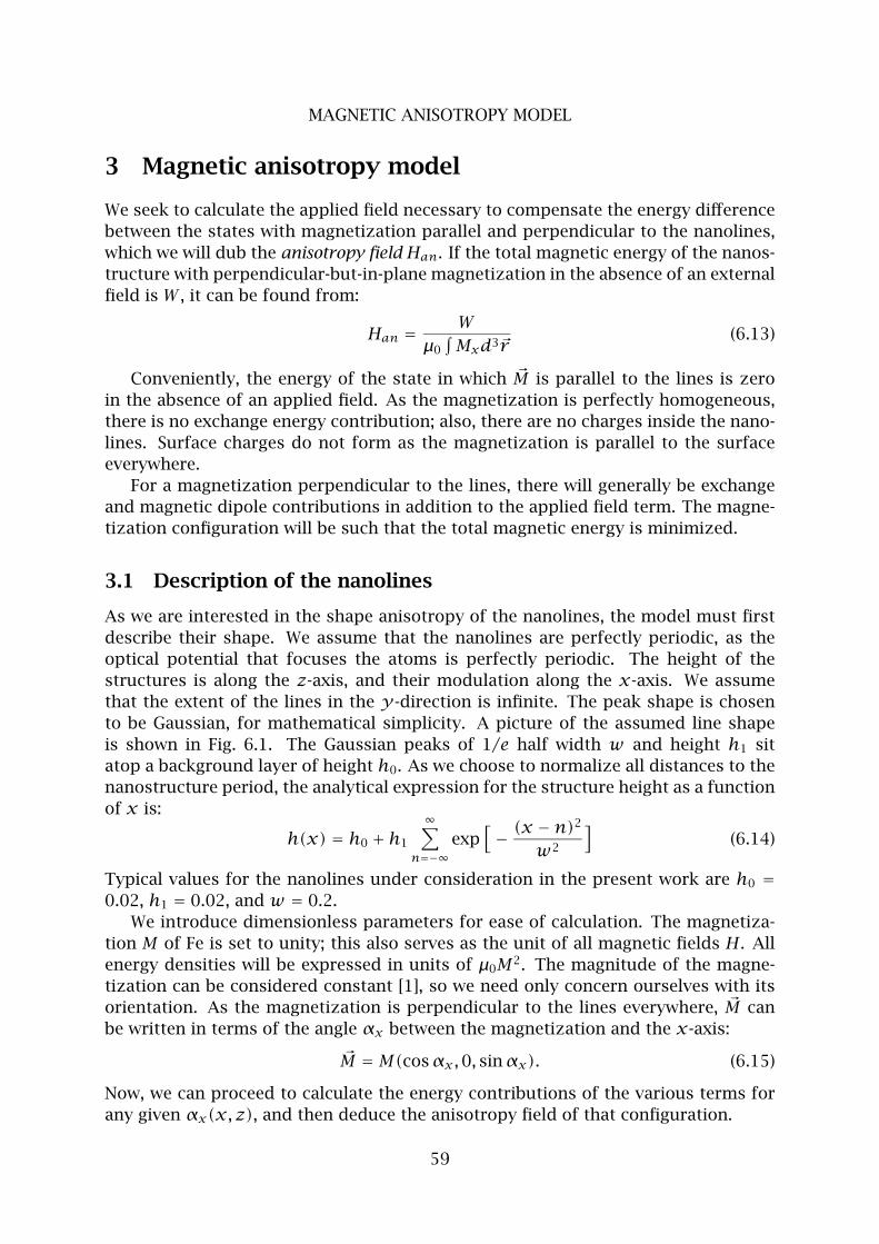
MAGNETIC ANISOTROPY MODEL
3 Magnetic anisotropy model
We seek to calculate the applied field necessary to compensate the energy difference
between the states with magnetization parallel and perpendicular to the nanolines,
which we will dub the anisotropy field Han. If the total magnetic energy of the nanos-
tructure with perpendicular-but-in-plane magnetization in the absence of an external
field is W , it can be found from:
Han =W
µ0
∫
Mxd3~r(6.13)
Conveniently, the energy of the state in which ~M is parallel to the lines is zero
in the absence of an applied field. As the magnetization is perfectly homogeneous,
there is no exchange energy contribution; also, there are no charges inside the nano-
lines. Surface charges do not form as the magnetization is parallel to the surface
everywhere.
For a magnetization perpendicular to the lines, there will generally be exchange
and magnetic dipole contributions in addition to the applied field term. The magne-
tization configuration will be such that the total magnetic energy is minimized.
3.1 Description of the nanolines
As we are interested in the shape anisotropy of the nanolines, the model must first
describe their shape. We assume that the nanolines are perfectly periodic, as the
optical potential that focuses the atoms is perfectly periodic. The height of the
structures is along the z-axis, and their modulation along the x-axis. We assume
that the extent of the lines in the y-direction is infinite. The peak shape is chosen
to be Gaussian, for mathematical simplicity. A picture of the assumed line shape
is shown in Fig. 6.1. The Gaussian peaks of 1/e half width w and height h1 sit
atop a background layer of height h0. As we choose to normalize all distances to the
nanostructure period, the analytical expression for the structure height as a function
of x is:
h(x) = h0 + h1
∞∑
n=−∞exp
[
− (x −n)2
w2
]
(6.14)
Typical values for the nanolines under consideration in the present work are h0 =0.02, h1 = 0.02, and w = 0.2.
We introduce dimensionless parameters for ease of calculation. The magnetiza-
tion M of Fe is set to unity; this also serves as the unit of all magnetic fields H. All
energy densities will be expressed in units of µ0M2. The magnitude of the magne-
tization can be considered constant [1], so we need only concern ourselves with its
orientation. As the magnetization is perpendicular to the lines everywhere, ~M can
be written in terms of the angle αx between the magnetization and the x-axis:
~M = M(cosαx,0, sinαx). (6.15)
Now, we can proceed to calculate the energy contributions of the various terms for
any given αx(x, z), and then deduce the anisotropy field of that configuration.
59
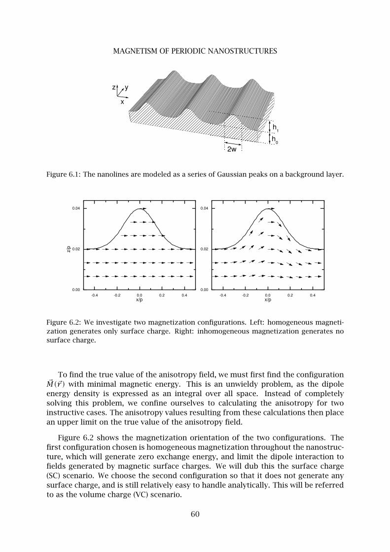
MAGNETISM OF PERIODIC NANOSTRUCTURES
z y
x
h0
h1
2w
Figure 6.1: The nanolines are modeled as a series of Gaussian peaks on a background layer.
-0.4 -0.2 0.0 0.2 0.40.00
0.02
0.04
x/p-0.4 -0.2 0.0 0.2 0.4
0.00
0.02
0.04
z/p
x/p
Figure 6.2: We investigate two magnetization configurations. Left: homogeneous magneti-
zation generates only surface charge. Right: inhomogeneous magnetization generates no
surface charge.
To find the true value of the anisotropy field, we must first find the configuration~M(~r) with minimal magnetic energy. This is an unwieldy problem, as the dipole
energy density is expressed as an integral over all space. Instead of completely
solving this problem, we confine ourselves to calculating the anisotropy for two
instructive cases. The anisotropy values resulting from these calculations then place
an upper limit on the true value of the anisotropy field.
Figure 6.2 shows the magnetization orientation of the two configurations. The
first configuration chosen is homogeneous magnetization throughout the nanostruc-
ture, which will generate zero exchange energy, and limit the dipole interaction to
fields generated by magnetic surface charges. We will dub this the surface charge
(SC) scenario. We choose the second configuration so that it does not generate any
surface charge, and is still relatively easy to handle analytically. This will be referred
to as the volume charge (VC) scenario.
60
MAGNETIC ANISOTROPY MODEL
3.2 SC model
We now proceed on the assumption that the magnetization of the nanoline is homo-
geneous over the entire structure, and is oriented along the x-axis with αx = 0. This
is the left configuration in Fig. 6.2. The surface charges are described by:
ρ∗ = −∇ · ~M = −δ(z − h(x,y)) ~M · ~n = δ(z − h(x,y))∂h∂x
√
1+ ( ∂h∂x)2. (6.16)
These expressions have been converted to the dimensionless units; the surface nor-
mal is referred to as ~n. The h-dependent part of the expression is simply a sine. As
we are looking for the anisotropy effect of the nanolines, we are interested mainly in
the x-component of the demagnetizing field. It is given by:
Hx(x,y, z) =1
4π
∫ ∫ ∂h∂x′ (x
′)√
1+ ( ∂h∂x′ (x
′))2
x − x′((x − x′)2 + (y −y ′)2 + (z − h(x′))2)3/2
dx′dy ′,
(6.17)
or, after integrating out the y-dependence:
Hx(x,y, z) =1
2π
∫ ∂h∂x′ (x
′)√
1+ ( ∂h∂x′ (x
′))2
x − x′(x − x′)2 + (z − h(x′))2dx
′. (6.18)
Similarly, the z component of the demagnetizing field can be shown to be:
Hz(x,y, z) =1
2π
∫ ∂h∂x′ (x
′)√
1+ ( ∂h∂x′ (x
′))2
z − h(x′)(x − x′)2 + (z − h(x′))2dx
′. (6.19)
Calculating the energy of the structure is simply the integral:
W
µ0M2= 1
2
∫
Hx(~r)d3~r , (6.20)
with the integration volume a cross-section of a nanoline over one full period by
some arbitrary y-length. This integration can be carried out numerically without
frustratingly large computation times.
3.3 VC model
We now explore another option, one that nulls the surface poles. The key physical
assumption in this model is the energetic dominance of surface poles over all else.
This assumption is made not because we believe it correct, but rather because we
want to investigate the other energy terms separately from the surface energy. We
impose the boundary condition:
α(x,h(x)) = arcsin∂h/∂x
√
1+ (∂h/∂x)2, (6.21)
61
MAGNETISM OF PERIODIC NANOSTRUCTURES
where h(x) is a function that describes the nanoline height profile. One guess at a
magnetization distribution α(x, z) is:
α(x, z) = α(x,h(x))∗ z
h(x), (6.22)
with α(x,h(x)) taken from Eq. 6.21. This expression is analytically very simple.
Also, it has a good chance at producing relatively low exchange energies, as its
derivative with respect to z is constant. The orientation of the magnetization vectors
is displayed on the right in Fig. 6.2. Given this distribution and the expressions for
the various energy terms, the rest is a matter of calculus.
The task of numerically computing the energy of these nanolines is not very
complicated, but it does require large amounts of calculation time if performed ex-
actly. The following will be a set of simplifications, so that the computation times
may remain limited and some physical insight may be gained. The most impor-
tant simplification will be the assumption that we deal with relatively low and broad
nanolines.
Exchange energy
The exchange energy density is a relatively straightforward energy density func-
tional, given the distribution α(x, z). From Eq. 6.8, it can be shown that:
Eex = Aex[(∂α
∂x)2 + (∂α
∂z)2]. (6.23)
The derivatives of α can be evaluated to:
∂α∂x= [
∂2h/∂x2
1+(∂h/∂x)2 −∂h/∂xh(x)
arcsin ∂h/∂x√1+(∂h/∂x)2
]z
h(x);
∂α∂z= 1
h(x)arcsin ∂h/∂x√
1+(∂h/∂x)2.
(6.24)
While this is enough to calculate exactly the exchange energy of any structure, we
are interested in low, wide nanolines, with widths typically in the tens of nanometers
and heights of a few nanometers. Thus, we may assume that h≪ w, and therefore
that ∂h/∂x ≪ 1. Keeping only terms in first order in the derivatives dramatically
simplifies them:∂α∂x= 0;
∂α∂z= ∂h
∂x1
h(x).
(6.25)
The exchange energy density is now approximated by:
Eex = Aex[∂h
∂x
1
h(x)
]2
. (6.26)
Converted into dimensionless units, the value of the exchange constant equals Aex =1.52× 10⁻⁴.
62
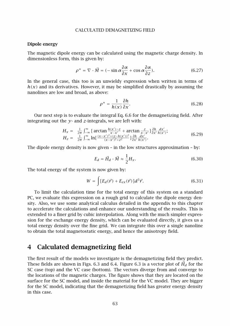
CALCULATED DEMAGNETIZING FIELD
Dipole energy
The magnetic dipole energy can be calculated using the magnetic charge density. In
dimensionless form, this is given by:
ρ∗ = ∇ · ~M = (− sinα∂α
∂x+ cosα
∂α
∂z). (6.27)
In the general case, this too is an unwieldy expression when written in terms of
h(x) and its derivatives. However, it may be simplified drastically by assuming the
nanolines are low and broad, as above:
ρ∗ = 1
h(x)
∂h
∂x. (6.28)
Our next step is to evaluate the integral Eq. 6.6 for the demagnetizing field. After
integrating out the y- and z-integrals, we are left with:
Hx = 12π
∫∞−∞ [ arctan h(x′)−z
x−x′ + arctan zx−x′ ]
∂h∂x′
dx′
h(x′) ;
Hz = 12π
∫∞−∞ ln[ (x−x
′)2+(z−h(x′))2(x−x′)2+z2 ] ∂h
∂x′dx′
h(x′) .(6.29)
The dipole energy density is now given – in the low structures approximation – by:
Ed = ~Hd · ~M ≈ 1
2Hx. (6.30)
The total energy of the system is now given by:
W =∫
[Ed(~r)+ Eex(~r)]d3~r . (6.31)
To limit the calculation time for the total energy of this system on a standard
PC, we evaluate this expression on a rough grid to calculate the dipole energy den-
sity. Also, we use some analytical calculus detailed in the appendix to this chapter
to accelerate the calculations and enhance our understanding of the results. This is
extended to a finer grid by cubic interpolation. Along with the much simpler expres-
sion for the exchange energy density, which can be evaluated directly, it gives us a
total energy density over the fine grid. We can integrate this over a single nanoline
to obtain the total magnetostatic energy, and hence the anisotropy field.
4 Calculated demagnetizing field
The first result of the models we investigate is the demagnetizing field they predict.
These fields are shown in Figs. 6.3 and 6.4. Figure 6.3 is a vector plot of ~Hd for the
SC case (top) and the VC case (bottom). The vectors diverge from and converge to
the locations of the magnetic charges. The figure shows that they are located on the
surface for the SC model, and inside the material for the VC model. They are bigger
for the SC model, indicating that the demagnetizing field has greater energy density
in this case.
63
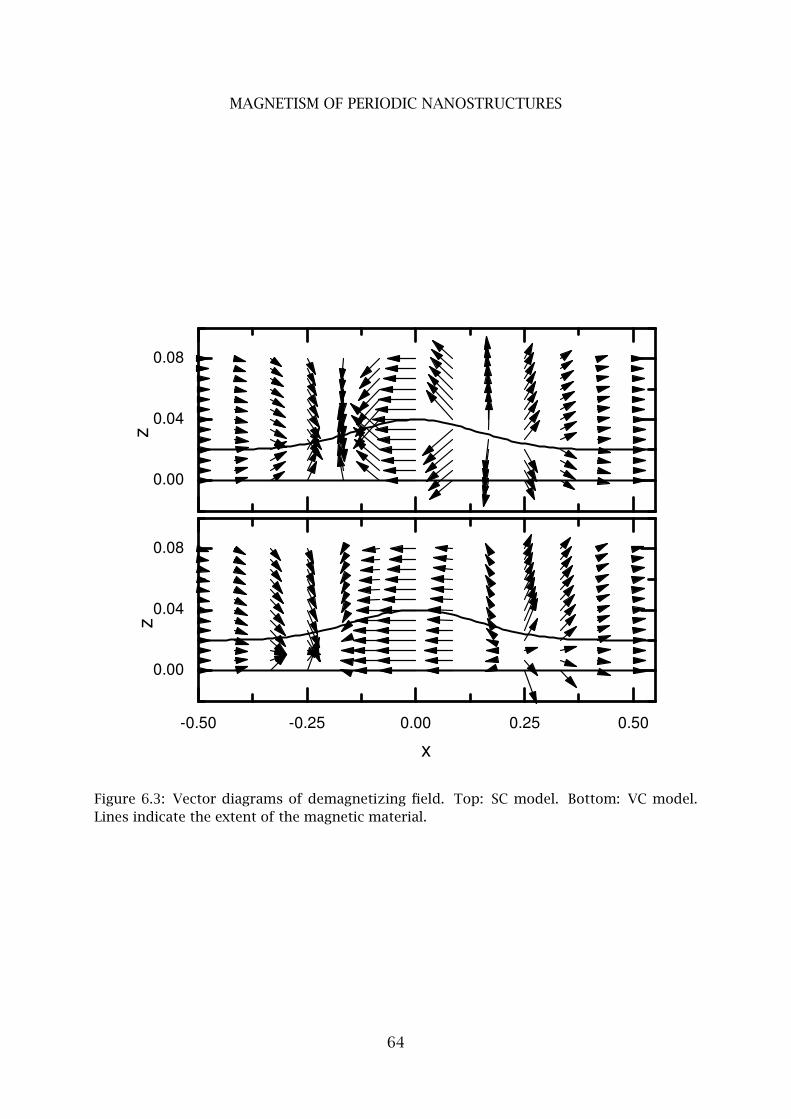
MAGNETISM OF PERIODIC NANOSTRUCTURES
-0.50 -0.25 0.00 0.25 0.50
0.00
0.04
0.08
z
x
0.00
0.04
0.08
z
Figure 6.3: Vector diagrams of demagnetizing field. Top: SC model. Bottom: VC model.
Lines indicate the extent of the magnetic material.
64
CALCULATED DEMAGNETIZING FIELD
b
-0.060
-0.030
0
0.030
0.060
0.00
0.05
0.10
0.15
a
z
-0.50 -0.25 0.00 0.25 0.50
0.00
0.05
0.10
0.15
x
c
z
-0.50 -0.25 0.00 0.25 0.50
x
d
Figure 6.4: Demagnetizing field for the SC model (a: x component; b: z component) and
the VC model (c: x component; d: z component). Lines indicate the extent of the magnetic
material.
65
MAGNETISM OF PERIODIC NANOSTRUCTURES
The x and z component of the field in the SC scenario are shown in Fig. 6.4 a and
b, respectively. Figure 6.4 c and d show the x and z components of Hd for the VC
case. Investigating the SC case, we find that the x component of Hd is opposite to
the magnetization direction inside the nanoline itself. This is its usual orientation,
hence the term ‘demagnetizing field’. In the background layer between the nano-
lines, however, its x component is aligned parallel to the magnetization. Although
this orientation may appear puzzling at first sight, it is less mysterious when consid-
ered in the magnetic charge view. The magnetization points out of the structure at
its right flank. Hence, a positive charge arises there. The next structure (not shown
in the figure) has a negative charge at its left flank. Hence, a field line will run from
one nanoline to the next that runs parallel to the magnetization. The total shape
anisotropy of the nanolines is now a sum of the energy cost of the nanolines and
the energy gain of the background layer in between. The z component (Fig. 6.4b)
shows the location of the surface poles very clearly. Though it does not contribute
to the anisotropy energy of the nanostructure as it is perpendicular to the magneti-
zation, it might in principle be used in stray field detection. Its advantage over the
x-component is that the latter has a relatively large applied field background, and
thus requires more sensitive detection.
For the VC case, the demagnetizing field x component (Fig. 6.4c) and z compo-
nent (Fig. 6.4d) are also shown. The picture of the x component is similar to its SC
counterpart. The main difference can be seen around x = ±0.3, where the demagne-
tizing field reaches a maximum. In contrast to the SC case in Fig. 6.4a, the maximum
is now inside the nanostructure. Hence, the contribution of the demagnetizing field
to the anisotropy field will be smaller. The z component of the demagnetizing field is
also smaller in the VC case, which stands to reason as the magnetic charge that gen-
erates it is spread out over a larger area. The most conspicuous feature of Fig. 6.4d
is the fact that the field maxima are located relatively far out to the sides of the
nanoline. We could find no obvious explanation for this phenomenon.
5 Calculated anisotropy field
We have run the simulations described above for both cases, choosing standard
settings: h0 = 0.02, h1 = 0.02, w = 0.2. This means that we have a set of Gaussian
peaks that are as high as the background, both being 3.72 nm high. The FWHM of
the peaks is 62 nm, which is realistic considering our deposition results. We will
vary the three parameters separately. Also, results are presented as a function of
the total atomic flux, and contrast ratio. A discussion of the results is provided.
Structure height
First, we vary the nanoline height h1. The results are shown in Fig. 6.5. In the SC case,
the anisotropy field is at first linear with respect to the nanoline height. This is to be
expected, as the surface charge density scales as ∂h/∂x. For high lines, the surface
charge density is less than would be expected from extrapolation of the linear case.
66
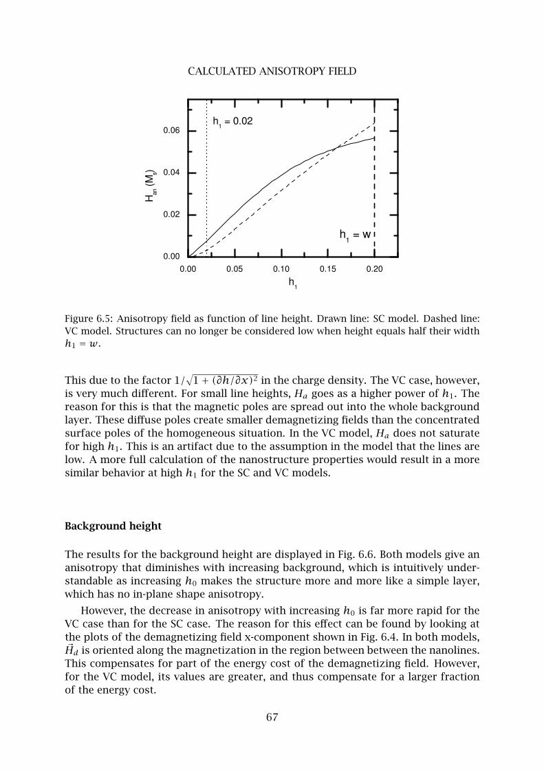
CALCULATED ANISOTROPY FIELD
0.00 0.05 0.10 0.15 0.20
0.00
0.02
0.04
0.06h
1 = 0.02
h1 = w
Han
(M
s)
h1
Figure 6.5: Anisotropy field as function of line height. Drawn line: SC model. Dashed line:
VC model. Structures can no longer be considered low when height equals half their width
h1 = w.
This due to the factor 1/√
1+ (∂h/∂x)2 in the charge density. The VC case, however,
is very much different. For small line heights, Ha goes as a higher power of h1. The
reason for this is that the magnetic poles are spread out into the whole background
layer. These diffuse poles create smaller demagnetizing fields than the concentrated
surface poles of the homogeneous situation. In the VC model, Ha does not saturate
for high h1. This is an artifact due to the assumption in the model that the lines are
low. A more full calculation of the nanostructure properties would result in a more
similar behavior at high h1 for the SC and VC models.
Background height
The results for the background height are displayed in Fig. 6.6. Both models give an
anisotropy that diminishes with increasing background, which is intuitively under-
standable as increasing h0 makes the structure more and more like a simple layer,
which has no in-plane shape anisotropy.
However, the decrease in anisotropy with increasing h0 is far more rapid for the
VC case than for the SC case. The reason for this effect can be found by looking at
the plots of the demagnetizing field x-component shown in Fig. 6.4. In both models,~Hd is oriented along the magnetization in the region between between the nanolines.
This compensates for part of the energy cost of the demagnetizing field. However,
for the VC model, its values are greater, and thus compensate for a larger fraction
of the energy cost.
67
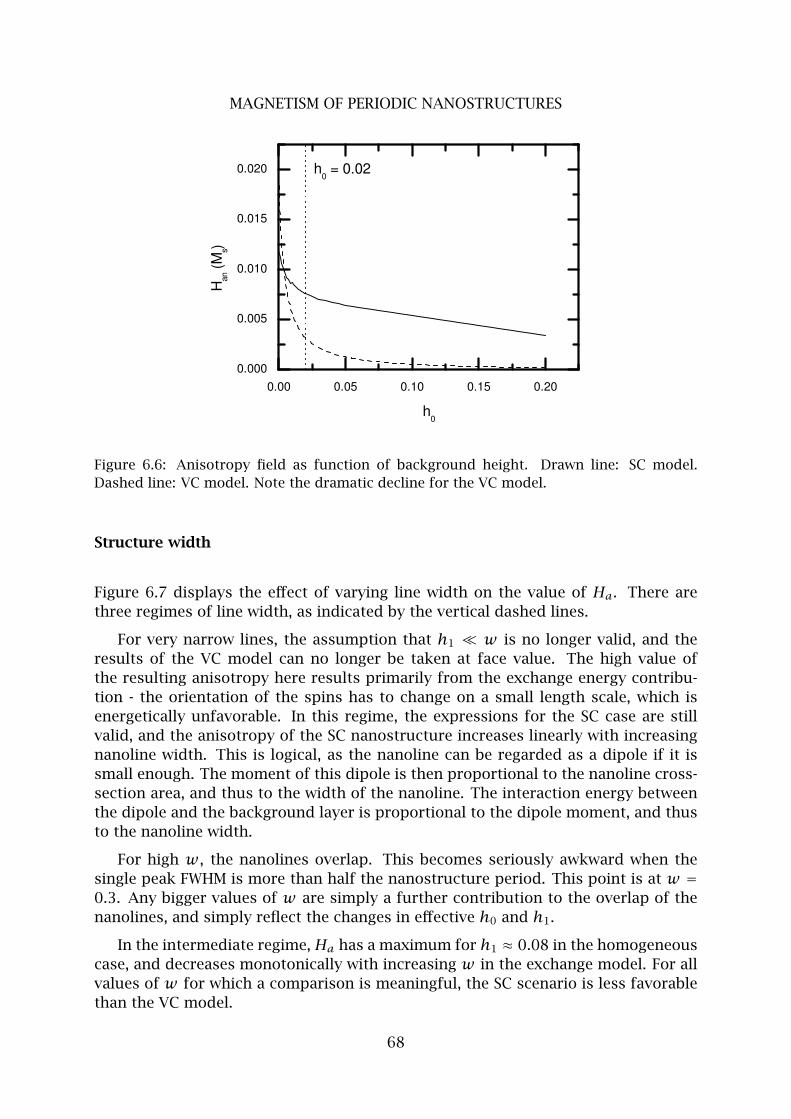
MAGNETISM OF PERIODIC NANOSTRUCTURES
0.00 0.05 0.10 0.15 0.20
0.000
0.005
0.010
0.015
0.020 h0 = 0.02
Han
(M
s)
h0
Figure 6.6: Anisotropy field as function of background height. Drawn line: SC model.
Dashed line: VC model. Note the dramatic decline for the VC model.
Structure width
Figure 6.7 displays the effect of varying line width on the value of Ha. There are
three regimes of line width, as indicated by the vertical dashed lines.
For very narrow lines, the assumption that h1 ≪ w is no longer valid, and the
results of the VC model can no longer be taken at face value. The high value of
the resulting anisotropy here results primarily from the exchange energy contribu-
tion - the orientation of the spins has to change on a small length scale, which is
energetically unfavorable. In this regime, the expressions for the SC case are still
valid, and the anisotropy of the SC nanostructure increases linearly with increasing
nanoline width. This is logical, as the nanoline can be regarded as a dipole if it is
small enough. The moment of this dipole is then proportional to the nanoline cross-
section area, and thus to the width of the nanoline. The interaction energy between
the dipole and the background layer is proportional to the dipole moment, and thus
to the nanoline width.
For high w, the nanolines overlap. This becomes seriously awkward when the
single peak FWHM is more than half the nanostructure period. This point is at w =0.3. Any bigger values of w are simply a further contribution to the overlap of the
nanolines, and simply reflect the changes in effective h0 and h1.
In the intermediate regime, Ha has a maximum for h1 ≈ 0.08 in the homogeneous
case, and decreases monotonically with increasing w in the exchange model. For all
values of w for which a comparison is meaningful, the SC scenario is less favorable
than the VC model.
68
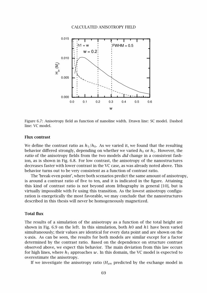
CALCULATED ANISOTROPY FIELD
0.0 0.1 0.2 0.3 0.4 0.5 0.6
0.000
0.005
0.010
0.015
w = 0.2
FWHM = 0.5h1 = w
Han
(M
s)
w
Figure 6.7: Anisotropy field as function of nanoline width. Drawn line: SC model. Dashed
line: VC model.
Flux contrast
We define the contrast ratio as h1/h0. As we varied it, we found that the resulting
behavior differed strongly, depending on whether we varied h0 or h1. However, the
ratio of the anisotropy fields from the two models did change in a consistent fash-
ion, as is shown in Fig. 6.8. For low contrast, the anisotropy of the nanostructures
decreases faster with lower contrast in the VC case, as was already noted above. This
behavior turns out to be very consistent as a function of contrast ratio.
The ’break-even point’, where both scenarios predict the same amount of anisotropy,
is around a contrast ratio of five to ten, and it is indicated in the figure. Attaining
this kind of contrast ratio is not beyond atom lithography in general [10], but is
virtually impossible with Fe using this transition. As the lowest anisotropy configu-
ration is energetically the most favorable, we may conclude that the nanostructures
described in this thesis will never be homogeneously magnetized.
Total flux
The results of a simulation of the anisotropy as a function of the total height are
shown in Fig. 6.9 on the left. In this simulation, both h0 and h1 have been varied
simultaneously; their values are identical for every data point and are shown on the
x-axis. As can be seen, the results for both models are similar except for a factor
determined by the contrast ratio. Based on the dependence on structure contrast
observed above, we expect this behavior. The main deviation from this law occurs
for high lines, where h1 approaches w. In this domain, the VC model is expected to
overestimate the anisotropy.
If we investigate the anisotropy ratio (Han predicted by the exchange model in
69
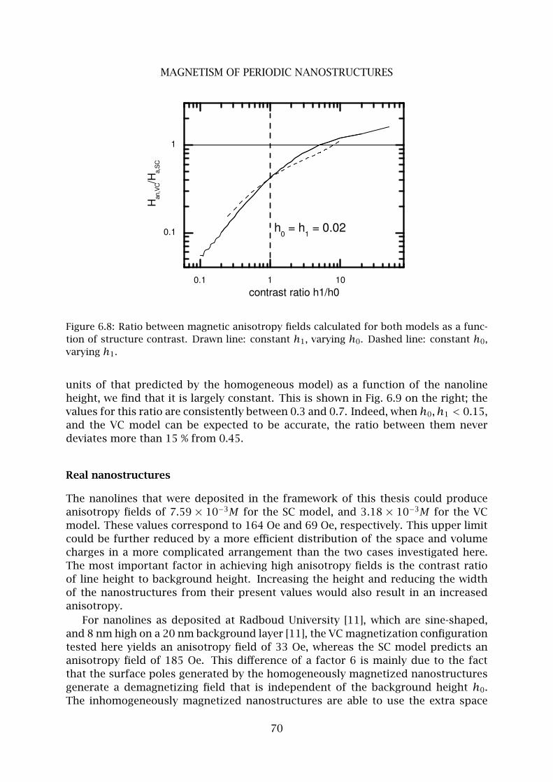
MAGNETISM OF PERIODIC NANOSTRUCTURES
0.1 1 10
0.1
1
h0 = h
1 = 0.02
Han
,VC/H
a,S
C
contrast ratio h1/h0
Figure 6.8: Ratio between magnetic anisotropy fields calculated for both models as a func-
tion of structure contrast. Drawn line: constant h1, varying h0. Dashed line: constant h0,
varying h1.
units of that predicted by the homogeneous model) as a function of the nanoline
height, we find that it is largely constant. This is shown in Fig. 6.9 on the right; the
values for this ratio are consistently between 0.3 and 0.7. Indeed, when h0, h1 < 0.15,
and the VC model can be expected to be accurate, the ratio between them never
deviates more than 15 % from 0.45.
Real nanostructures
The nanolines that were deposited in the framework of this thesis could produce
anisotropy fields of 7.59 × 10⁻³M for the SC model, and 3.18 × 10⁻³M for the VC
model. These values correspond to 164 Oe and 69 Oe, respectively. This upper limit
could be further reduced by a more efficient distribution of the space and volume
charges in a more complicated arrangement than the two cases investigated here.
The most important factor in achieving high anisotropy fields is the contrast ratio
of line height to background height. Increasing the height and reducing the width
of the nanostructures from their present values would also result in an increased
anisotropy.
For nanolines as deposited at Radboud University [11], which are sine-shaped,
and 8 nm high on a 20 nm background layer [11], the VC magnetization configuration
tested here yields an anisotropy field of 33 Oe, whereas the SC model predicts an
anisotropy field of 185 Oe. This difference of a factor 6 is mainly due to the fact
that the surface poles generated by the homogeneously magnetized nanostructures
generate a demagnetizing field that is independent of the background height h0.
The inhomogeneously magnetized nanostructures are able to use the extra space
70
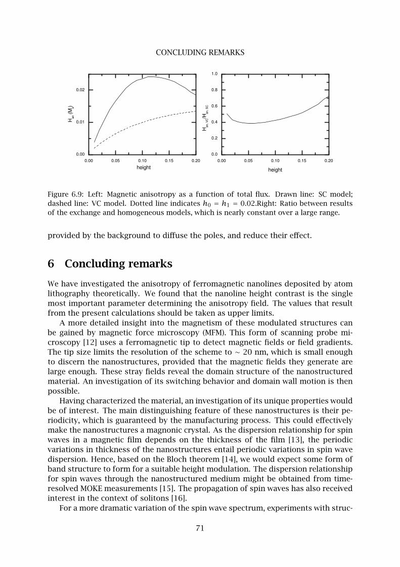
CONCLUDING REMARKS
0.00 0.05 0.10 0.15 0.20
0.00
0.01
0.02
H
an (
Ms)
height0.00 0.05 0.10 0.15 0.20
0.0
0.2
0.4
0.6
0.8
1.0
Han
, VC/H
an, S
C
height
Figure 6.9: Left: Magnetic anisotropy as a function of total flux. Drawn line: SC model;
dashed line: VC model. Dotted line indicates h0 = h1 = 0.02.Right: Ratio between results
of the exchange and homogeneous models, which is nearly constant over a large range.
provided by the background to diffuse the poles, and reduce their effect.
6 Concluding remarks
We have investigated the anisotropy of ferromagnetic nanolines deposited by atom
lithography theoretically. We found that the nanoline height contrast is the single
most important parameter determining the anisotropy field. The values that result
from the present calculations should be taken as upper limits.
A more detailed insight into the magnetism of these modulated structures can
be gained by magnetic force microscopy (MFM). This form of scanning probe mi-
croscopy [12] uses a ferromagnetic tip to detect magnetic fields or field gradients.
The tip size limits the resolution of the scheme to ∼ 20 nm, which is small enough
to discern the nanostructures, provided that the magnetic fields they generate are
large enough. These stray fields reveal the domain structure of the nanostructured
material. An investigation of its switching behavior and domain wall motion is then
possible.
Having characterized the material, an investigation of its unique properties would
be of interest. The main distinguishing feature of these nanostructures is their pe-
riodicity, which is guaranteed by the manufacturing process. This could effectively
make the nanostructures a magnonic crystal. As the dispersion relationship for spin
waves in a magnetic film depends on the thickness of the film [13], the periodic
variations in thickness of the nanostructures entail periodic variations in spin wave
dispersion. Hence, based on the Bloch theorem [14], we would expect some form of
band structure to form for a suitable height modulation. The dispersion relationship
for spin waves through the nanostructured medium might be obtained from time-
resolved MOKE measurements [15]. The propagation of spin waves has also received
interest in the context of solitons [16].
For a more dramatic variation of the spin wave spectrum, experiments with struc-
71
MAGNETISM OF PERIODIC NANOSTRUCTURES
tured doping could be considered. Codepositing another ferromagnetic material
would result in a magnetic layer of periodically varying composition. This, too,
would affect the dispersion relationship of the spin waves, resulting a magnonic crys-
tal. These experiments could be of great interest for spintronics applications [17].
References
[1] E. du Tremolet de Lacheisserie, D. Gignoux, M. Schlenker, Eds., Magnetism, Kluwer
Academic, Dordrecht (2002)
[2] A. J. Bennett and J. M. Xu, Appl. Phys. Lett. 82 3304-3306 (2003)
[3] Y. Peng, T.-H. Shen, B. Ashworth, X.-G. Zhao, C. A. Faunce, and Y.-W. Liu, Appl. Phys.
Lett. 83, 362-364 (2003)
[4] W. C. Uhlig and J. Shi, Appl. Phys. Lett. 84, 759-762 (2004); J. I. Martın, M. Velez, R.
Morales, J. M. Alameda, J. V. Anguita, F. Briones, and J. L. Vincent, J. Magn. Magn.
Mater. 249, 156-162 (2002)
[5] D. J. Griffiths, Introduction to Electrodynamics, 2nd Ed., Prentice-Hall, Englewood Cliffs
(1989)
[6] L. M. Magid, Electromagnetic Fields, Energy, and Waves, J. Wiley and Sons, New York
(1972)
[7] D. J. Griffiths, Introduction to Quantum Mechanics, 2nd Ed., Prentice Hall, Englewood
Cliffs (1995)
[8] C. Kittel, Rev. Mod. Phys. 21, 541-583 (1949)
[9] D. Rugar, H. J. Mamin, S. E. Lambert, J. E. Stern, I. McFadyen, and T. Yogi, J. Appl. Phys.
68, 1169-1183 (1990)
[10] V. Natarajan, R.E. Behringer, G. Timp, Phys Rev. A53, 4381-4385 (1996)
[11] G. Myszkiewicz, J. Hohlfeld, A. J. Toonen, A. F. van Etteger, O. I. Shklyarevskii, W. L.
Meerts, and Th. Rasing, Appl. Phys. Lett. 85, 3482 (2004)
[12] D. Sarid, Scanning Force Microscopy, Oxford University Press, Oxford (1994)
[13] B. Hillebrands and K. Ounadjela (Eds.), Spin Dynamics in Confined Magnetic Structures
I, Springer, Heidelberg (2002)
[14] C. Kittel, Introduction to solid state physics, 7th Ed., J. Wiley and Sons, New York
(1996)
[15] M. van Kampen, C. Jozsa, J. T. Kohlhepp, P. LeClair, L. Lagae, W. J. M. de Jonge, and B.
Koopmans, Phys. Rev. Lett. 88, 227201 (2002)
[16] J. W. Fleischer, M. Segev, N. K. Efremidis, D. N. Christodoulides, Nature 422, 147 - 150
(2003)
72
CONCLUDING REMARKS
[17] D. Awschalom, R. A. Buhrman, J. M. Daughton, S. von Molnar, and M. L. Roukes, Eds.,
Spin Electronics, Kluwer Academic, Dordrecht (2004)
73
MAGNETISM OF PERIODIC NANOSTRUCTURES
A Appendix
Empirically, it was found that the calculation of the energy of the VC magnetic con-
figuration was still a very time-consuming process, as the integral for the demagne-
tizing field is very slow to converge. This can be seen by looking at the integrand,
which goes as 1/x′ for large x′; thus, the integral only converges because ∂h/∂x′
periodically changes sign.
We therefore look for an analytical way to estimate the integral. This may be done
by splitting the integral in three parts – one for x′ < −xc , one for −xc < x′ < xc and
one for xc < x′. In the central part, the arctangents are crucial to keep the integrand
finite, and the integral is evaluated explicitly. In the outer parts, we approximate the
integrand by:
[ arctanh(x′)− zx − x′ + arctan
z
x − x′ ]∂h
∂x′dx′
h(x′)≈ 1
x − x′∂h
∂x′dx′. (6.32)
This approximation is valid provided that xc ≫ max(h), z. The integral now
becomes:∫∞
xc
∂h
∂x′dx′
x − x′ . (6.33)
Integration by parts yields:
∫∞
xc
∂h
∂x′dx′
x − x′ =h(xc)
xc − x−∫∞
xc
h(x′)
(x − x′)2dx′. (6.34)
This integral will at least converge much faster, but it can be estimated analytically.
In fact, if we assume that the Gaussian peaks are well-separated (exp(−0.25/w2)≪1) or roughly w <
√2/4 ≈ 0.35, the contribution of a single peak around x − x′ =
n, |n| ≫ x,w can be approximated further:
∫∞xc
h1 exp(−(x′−n)2/w2)(x−x′)2 dx′ =
∫∞xc−n
h1 exp(−y2/w2)(x+n−y)2 dy
=∫∞xc−n
h1 exp(−y2/w2)(1−(y/(x+n))2 dy ×
1(n+x)2
≈ h1w√π
n2 .
(6.35)
The approximation is possible because the Gaussian is zero except around y ≈0, and the derivatives of the function by which it is multiplied are very small at
this point. Summing this result over all n yields h1w√π × π2/6, and we must
only subtract the terms from that sum that we include in the numerically evaluated
integral.
Now the contribution of a background term h0 to the integral becomes:
∫∞
xc
h0
(x − x′)2dx′ = h0
x − xc. (6.36)
Putting the previous results together, we arrive at a result for the tail integral:
∫∞
xc
∂h
∂x′dx′
x − x′ =h(xc)− h0
x − xc− h1w
√π[π2
6−nc−1∑
n=1
1
n2]. (6.37)
74
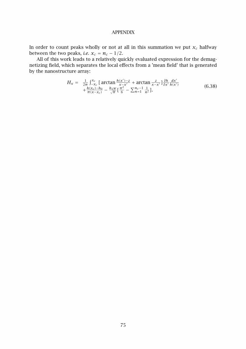
APPENDIX
In order to count peaks wholly or not at all in this summation we put xc halfway
between the two peaks, i.e. xc = nc − 1/2.
All of this work leads to a relatively quickly evaluated expression for the demag-
netizing field, which separates the local effects from a ’mean field’ that is generated
by the nanostructure array:
Hx = 12π
∫ xc−xc [ arctan h(x′)−z
x−x′ + arctan zx−x′ ]
∂h∂x′
dx′
h(x′)
+h(xc)−h0
π(x−xc) −h1w√π [
π2
6−∑nc−1n=1
1n2 ].
(6.38)
75

QUANTUM FEATURES IN ATOMIC NANOFABRICATION. . .
76
Chapter 7
Quantum Features in Atomic
Nanofabrication using Exactly Resonant
Standing Waves
The work described in this chapter was done at the University of Konstanz. The text
has been published in Phys. Rev. Lett. 93, 237402 (2004).
The ability to control the motion of atoms utilizing the atom-light interaction
has led to new fundamental physics such as laser cooling [1], Bose-Einstein conden-
sation [2], and precision experiments [3]. The control of the trajectories of atoms
has also found its way to applied science and allows the fabrication of nanostruc-
tures [4,5].
The basic idea of atomic nanofabrication is the controlled deposition of atoms
on a surface. This is achieved by employing spatially varying light forces, realized
in standard atomic nanofabrication with off resonant standing light waves. These
forces are well described within a classical atom-light interaction model [5]; how-
ever, this picture implies that these forces vanish for exactly resonant light fields.
Thus no nanostructures are expected, whereas the quantum mechanical treatment
of the atom-light interaction predicts the formation of structures for exactly reso-
nant standing light waves. Furthermore, the detailed analysis of the formed pattern
reveals that in contrast to the off resonant case the spatial phase of the light field
plays a crucial role for the quantum mechanical motion of the atoms. Additionally,
this system represents a new method for generating periodic patterns with feature
spacing smaller than the periodicity of the light intensity distribution. Introducing a
detuning in the order of the natural linewidth periodic nanostructures with doubled
periodicity can be fabricated. This adds a new scheme to the previously proposed
and demonstrated methods to beat the λ/2 periodicity limit of standard nanofabri-
cation [6–8].
In our experiments a chromium atomic beam is collimated to a divergence of
less than 1 mrad (full width at half maximum) by one-dimensional laser cooling
in a lin⊥lin configuration. The atomic beam impinges perpendicular onto the ex-
actly resonant standing light wave (7S3 →7P4 at λ=425.6 nm) which is realized by
77
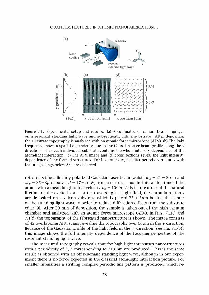
QUANTUM FEATURES IN ATOMIC NANOFABRICATION. . .
Figure 7.1: Experimental setup and results. (a) A collimated chromium beam impinges
on a resonant standing light wave and subsequently hits a substrate. After deposition
the substrate topography is analyzed with an atomic force microscope (AFM). (b) The Rabi
frequency shows a spatial dependence due to the Gaussian laser beam profile along the y
direction. Thus each individual substrate contains the whole intensity dependence of the
atom-light interaction. (c) The AFM image and (d) cross sections reveal the light intensity
dependence of the formed structures. For low intensity, peculiar periodic structures with
feature spacings below λ/2 are observed.
retroreflecting a linearly polarized Gaussian laser beam (waists wz = 21± 3µ m and
wy = 35±3µm, power P = 17±2mW) from a mirror. Thus the interaction time of the
atoms with a mean longitudinal velocity vz = 1000m/s is on the order of the natural
lifetime of the excited state. After traversing the light field, the chromium atoms
are deposited on a silicon substrate which is placed 35 ± 5µm behind the center
of the standing light wave in order to reduce diffraction effects from the substrate
edge [9]. After 30 min of deposition, the sample is taken out of the high vacuum
chamber and analyzed with an atomic force microscope (AFM). In Figs. 7.1(c) and
7.1(d) the topography of the fabricated nanostructure is shown. The image consists
of 42 overlapping AFM scans revealing the topography over 60µm in the y direction.
Because of the Gaussian profile of the light field in the y direction [see Fig. 7.1(b)],
this image shows the full intensity dependence of the focusing properties of the
resonant standing light wave.
The measured topography reveals that for high light intensities nanostructures
with a periodicity of λ/2 corresponding to 213 nm are produced. This is the same
result as obtained with an off resonant standing light wave, although in our exper-
iment there is no force expected in the classical atom-light interaction picture. For
smaller intensities a striking complex periodic line pattern is produced, which re-
78
QUANTUM FEATURES IN ATOMIC NANOFABRICATION. . .
veals lines spaced at 213 nm and additional features in between. We show that this
feature can be attributed to the quantum nature of the atom-light interaction and of
the atomic propagation.
First we give a qualitative discussion of the obtained experimental results in the
framework of dressed states. We then discuss our quantum mechanical simulations
which even allow a quantitative comparison between theory and experiment.
Dressed states are the eigenstates of the coupled atom-light system and are su-
perpositions of the eigenstates of the uncoupled atom |g〉 and |e〉. In the exactly
resonant case the dressed states and their energy are very simple [10] and are given
by:
|±; ~r〉 = 1√2(e−iφ(~r)/2|g〉 ± eiφ(~r)/2|e〉), E± = ±
2|Ω(~r)|, (7.1)
where the atom-light coupling is characterized by the complex Rabi frequencyΩ(~r) =−2 ~d · ~E(~r) = |Ω(~r)|eiφ(~r) , ~d is the atomic electric-dipole moment, and ~E represents
the electric field amplitude of the light field.
For a perfect standing light wave, the dressed states are degenerate at the nodes
where the electric field vanishes and thus E+ = E− = 0. This degeneracy is lifted
in our experiment, because we use a mirror with a reflectivity of R = 94%. The cor-
responding intensity distribution and resulting complex Rabi frequency is depicted
in Fig. 7.2(a). It is important to note that the phase of the Rabi frequency changes
dramatically at the nodes of the standing light wave that breaks the symmetry of the
light field there. In Fig. 7.2(b) the corresponding dressed state energies are shown
and the motion of a ground state atom is indicated.
In the regions where the Rabi frequency has a weak phase dependence the evo-
lution of a ground state atom is given by the corresponding dressed states, whose
motions are governed by Newtons equations of motion resulting from the corre-
sponding potential E+ and E−. In standard nanofabrication utilizing far off reso-
nance light forces the ground state atom is very well described by only one dressed
state (blue detuning mainly |+〉). But in an exactly resonant light field a ground state
atom is described as a fifty-fifty superposition of the two dressed states |+〉 and |−〉.Thus an atomic wave packet in a light field gradient will split into two parts. The
|−〉 is attracted to the intensity maxima while the |+〉 state is pulled to the inten-
sity minima as indicated in Fig. 7.2(b). This splitting is known as the optical Stern
Gerlach effect [11] and has already been observed by looking at the momentum dis-
tribution [12]. In our experiment we directly observe this effect by detecting the
atomic position on the nanometer scale.
The motion in the |−〉-state potential is almost perfectly harmonic close to its
minimum and concentrates the atoms like a lens for matter waves. This is very
similar to the standard atomic nanofabrication schemes. The |+〉-state potential
has a triangular shape in the vicinity of its minimum and corresponds to an atom
optical axicon, which produces a focal line. Since the distance between adjacent |+〉-state and |−〉-state potential minima is λ/4, nanostructures with half the standard
periodicity limit of λ/2 are expected.
The experimental observation that these λ/4 structures are not found for high
light intensity can easily be understood by realizing that nonadiabatic (NA) transi-
79
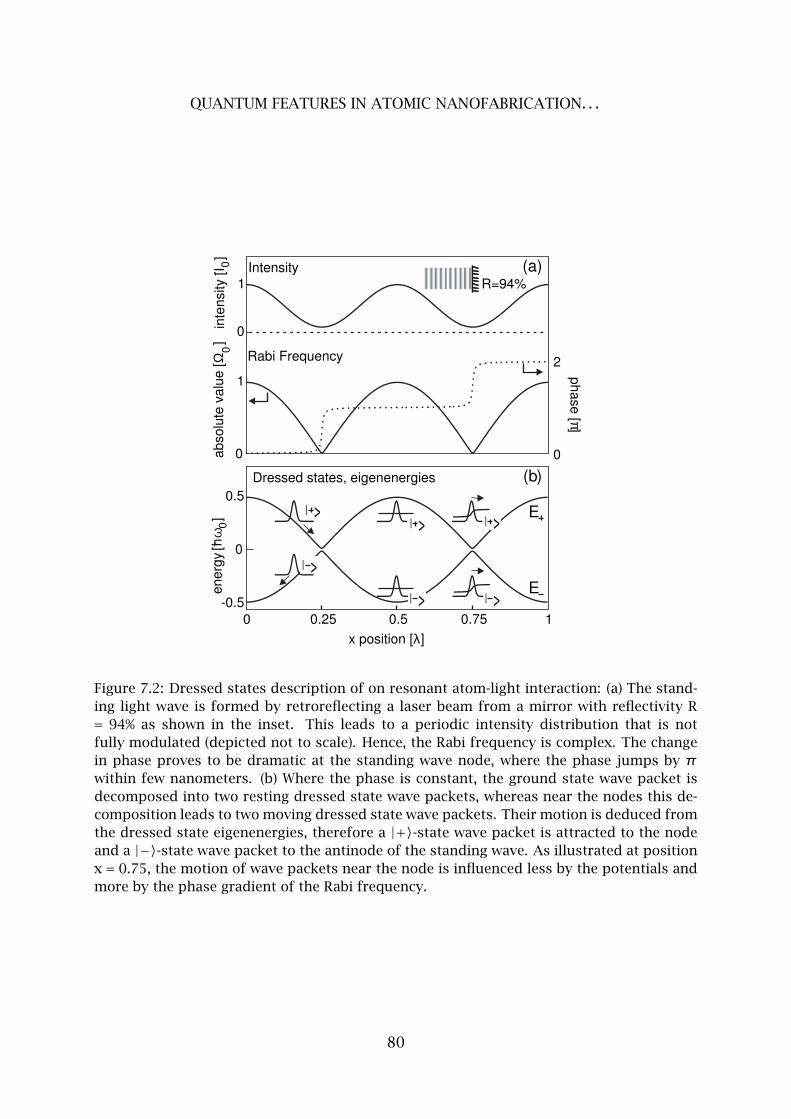
QUANTUM FEATURES IN ATOMIC NANOFABRICATION. . .
0
1
0
2
ph
ase
[π]
Rabi Frequency
ab
so
lute
va
lue
[Ω
]
1
0
R=94%
Intensity
inte
nsity [
I ] 0
0
0.5
en
erg
yh[
]
0
-0.5
Dressed states, eigenenergies
| >
| >| > | >
| > | >0 0.5 10.25 0.75
x position [λ]
E
E
(a)
(b)
0ω
Figure 7.2: Dressed states description of on resonant atom-light interaction: (a) The stand-
ing light wave is formed by retroreflecting a laser beam from a mirror with reflectivity R
= 94% as shown in the inset. This leads to a periodic intensity distribution that is not
fully modulated (depicted not to scale). Hence, the Rabi frequency is complex. The change
in phase proves to be dramatic at the standing wave node, where the phase jumps by π
within few nanometers. (b) Where the phase is constant, the ground state wave packet is
decomposed into two resting dressed state wave packets, whereas near the nodes this de-
composition leads to two moving dressed state wave packets. Their motion is deduced from
the dressed state eigenenergies, therefore a |+〉-state wave packet is attracted to the node
and a |−〉-state wave packet to the antinode of the standing wave. As illustrated at position
x = 0.75, the motion of wave packets near the node is influenced less by the potentials and
more by the phase gradient of the Rabi frequency.
80
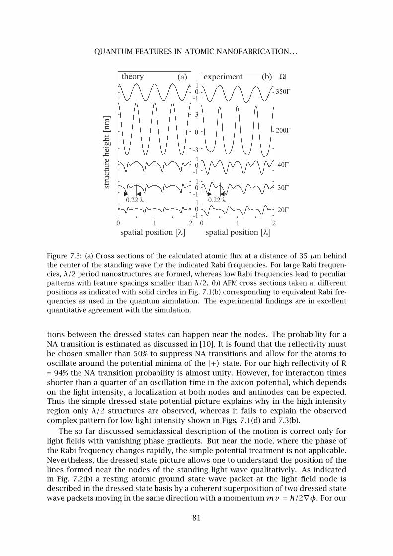
QUANTUM FEATURES IN ATOMIC NANOFABRICATION. . .
Figure 7.3: (a) Cross sections of the calculated atomic flux at a distance of 35 µm behind
the center of the standing wave for the indicated Rabi frequencies. For large Rabi frequen-
cies, λ/2 period nanostructures are formed, whereas low Rabi frequencies lead to peculiar
patterns with feature spacings smaller than λ/2. (b) AFM cross sections taken at different
positions as indicated with solid circles in Fig. 7.1(b) corresponding to equivalent Rabi fre-
quencies as used in the quantum simulation. The experimental findings are in excellent
quantitative agreement with the simulation.
tions between the dressed states can happen near the nodes. The probability for a
NA transition is estimated as discussed in [10]. It is found that the reflectivity must
be chosen smaller than 50% to suppress NA transitions and allow for the atoms to
oscillate around the potential minima of the |+〉 state. For our high reflectivity of R
= 94% the NA transition probability is almost unity. However, for interaction times
shorter than a quarter of an oscillation time in the axicon potential, which depends
on the light intensity, a localization at both nodes and antinodes can be expected.
Thus the simple dressed state potential picture explains why in the high intensity
region only λ/2 structures are observed, whereas it fails to explain the observed
complex pattern for low light intensity shown in Figs. 7.1(d) and 7.3(b).
The so far discussed semiclassical description of the motion is correct only for
light fields with vanishing phase gradients. But near the node, where the phase of
the Rabi frequency changes rapidly, the simple potential treatment is not applicable.
Nevertheless, the dressed state picture allows one to understand the position of the
lines formed near the nodes of the standing light wave qualitatively. As indicated
in Fig. 7.2(b) a resting atomic ground state wave packet at the light field node is
described in the dressed state basis by a coherent superposition of two dressed state
wave packets moving in the same direction with a momentummv = /2∇φ. For our
81
QUANTUM FEATURES IN ATOMIC NANOFABRICATION. . .
experimental situation we estimate the velocity of these wave packets to be ∼ 26vrwhere vr = k/m = 1.8 cm/s is the recoil velocity and k is the wave number of the
light. Thus one expects that atoms in the |+〉 state near the node run up the potential
due to this velocity [indicated in Fig. 7.2(b)]. An estimate of the expected shift after a
certain time can be found by calculating the classical trajectory of a particle starting
at the node with an initial velocity ∼ 26vr in the linear potential V(x) = k|Ω|x/2.
For the interaction time of 40 ns and a Rabi frequency of |Omega| = 20Γ we find the
position to be shifted by 14 nm from the node. Experimentally we observe 12±3 nm.
This effect is very closely connected to the scattering force [11] commonly applied
in laser cooling. There the situation is usually much simpler since the populations
of the dressed states can be assumed to be in steady state, while in our experiment
this is not the case.
Therefore to understand our experimental findings quantitatively we numerically
solve the Schrodinger equation for the two-level atom in momentum space [13].
Here, the two-level approach is reasonable as long as the intensive linearly polar-
ized light field defines the quantization axis and thus couples only magnetic sub-
states with equal quantum number (∆m = 0). This is strictly speaking not true near
the nodes. Therefore we numerically calculated the eigenenergies near the intensity
minimum including the earth magnetic field for arbitrary directions.We find that the
resulting eigenenergies are always symmetric with respect to the node of the stand-
ing light wave. Additionally the spatial range where anticrossings [6] between a few
of the involved energy levels occur is ±4 nm, which is the region where the dynam-
ics is governed anyway by NA transitions. In order to get a quantitative agreement
between the experimental findings and the numerical solution we include the effect
of spontaneous emissions empirically. According to the dressed state analysis given
in [10], spontaneous emissions can change the dressed state leading to momentum
diffusion due to the instantaneous sign reversal of the dipole force (the recoil kick
of the emitted photon is negligible). After the interaction time t this momentum
diffusion translates into a feature broadening ∆x(Ω)∝ vrΩt/Γ . To account for this
broadening a convolution of the calculated spatial probability distribution (taking
into account the divergence of the beam) with a Gaussian of width ∆x(Ω) is ap-
plied. This convolution is important only at high light intensities while it does not
significantly influence the structure shape at low light intensities. The additional
broadening effect due to the growth behavior of Cr [9] is negligible for our broad
structures (70 nm).
Cross sections of the calculated atomic flux at a distance of 35 µm behind the
center of the standing wave are shown in Fig. 7.3(a) and compared to the experi-
mental findings shown in Fig. 7.3(b). The experimental cross sections are taken at
positions indicated in Fig. 7.1(b) with solid circles. The theoretical curves shown
are obtained for the indicated Rabi frequencies. These values are consistent within
the uncertainty of the independently measured incoming power and beam waists.
Furthermore, we take into account the internal magnetic substructure of chromium
by multiplying the calculated Rabi frequency by a factor of 0.65 (average Clebsch-
Gordan coefficient for linear polarization), assuming equally populated substates.
This is valid in our case because the atoms travel 1 m in a magnetically unshielded
82
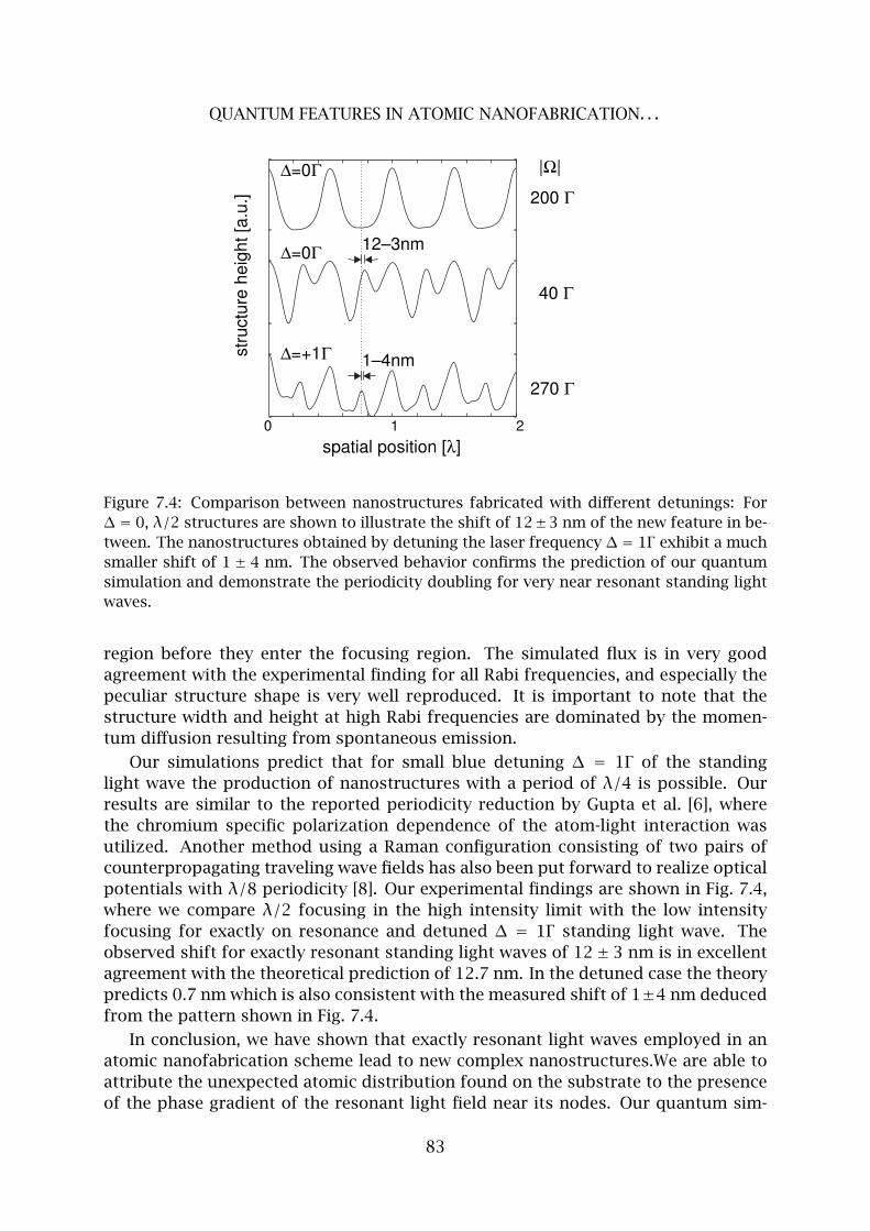
QUANTUM FEATURES IN ATOMIC NANOFABRICATION. . .
12–3nm
0 1 2
spatial position [λ]
str
uctu
re h
eig
ht
[a.u
.]
∆=0Γ
∆=0Γ
∆=+1Γ 1–4nm
|Ω|
270 Γ
40 Γ
200 Γ
Figure 7.4: Comparison between nanostructures fabricated with different detunings: For
∆ = 0, λ/2 structures are shown to illustrate the shift of 12±3 nm of the new feature in be-
tween. The nanostructures obtained by detuning the laser frequency ∆ = 1Γ exhibit a much
smaller shift of 1 ± 4 nm. The observed behavior confirms the prediction of our quantum
simulation and demonstrate the periodicity doubling for very near resonant standing light
waves.
region before they enter the focusing region. The simulated flux is in very good
agreement with the experimental finding for all Rabi frequencies, and especially the
peculiar structure shape is very well reproduced. It is important to note that the
structure width and height at high Rabi frequencies are dominated by the momen-
tum diffusion resulting from spontaneous emission.
Our simulations predict that for small blue detuning ∆ = 1Γ of the standing
light wave the production of nanostructures with a period of λ/4 is possible. Our
results are similar to the reported periodicity reduction by Gupta et al. [6], where
the chromium specific polarization dependence of the atom-light interaction was
utilized. Another method using a Raman configuration consisting of two pairs of
counterpropagating traveling wave fields has also been put forward to realize optical
potentials with λ/8 periodicity [8]. Our experimental findings are shown in Fig. 7.4,
where we compare λ/2 focusing in the high intensity limit with the low intensity
focusing for exactly on resonance and detuned ∆ = 1Γ standing light wave. The
observed shift for exactly resonant standing light waves of 12± 3 nm is in excellent
agreement with the theoretical prediction of 12.7 nm. In the detuned case the theory
predicts 0.7 nm which is also consistent with the measured shift of 1±4 nm deduced
from the pattern shown in Fig. 7.4.
In conclusion, we have shown that exactly resonant light waves employed in an
atomic nanofabrication scheme lead to new complex nanostructures.We are able to
attribute the unexpected atomic distribution found on the substrate to the presence
of the phase gradient of the resonant light field near its nodes. Our quantum sim-
83
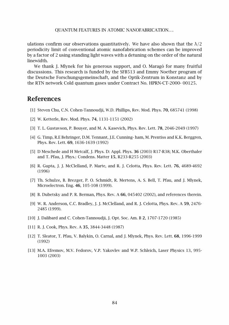
QUANTUM FEATURES IN ATOMIC NANOFABRICATION. . .
ulations confirm our observations quantitatively. We have also shown that the λ/2
periodicity limit of conventional atomic nanofabrication schemes can be improved
by a factor of 2 using standing light waves with a detuning on the order of the natural
linewidth.
We thank J. Mlynek for his generous support, and O. Marago for many fruitful
discussions. This research is funded by the SFB513 and Emmy Noether program of
the Deutsche Forschungsgemeinschaft, and the Optik-Zentrum in Konstanz and by
the RTN network Cold quantum gases under Contract No. HPRN-CT-2000- 00125.
References
[1] Steven Chu, C.N. Cohen-Tannoudji, W.D. Phillips, Rev. Mod. Phys. 70, 685741 (1998)
[2] W. Ketterle, Rev. Mod. Phys. 74, 1131-1151 (2002)
[3] T. L. Gustavson, P. Bouyer, and M. A. Kasevich, Phys. Rev. Lett. 78, 2046-2049 (1997)
[4] G. Timp, R.E Behringer, D.M. Tennant, J.E. Cunning- ham, M. Prentiss and K.K. Berggren,
Phys. Rev. Lett. 69, 1636-1639 (1992)
[5] D Meschede and H Metcalf, J. Phys. D: Appl. Phys. 36 (2003) R17-R38; M.K. Oberthaler
and T. Pfau, J. Phys.: Condens. Matter 15, R233-R255 (2003)
[6] R. Gupta, J. J. McClelland, P. Marte, and R. J. Celotta, Phys. Rev. Lett. 76, 4689-4692
(1996)
[7] Th. Schulze, B. Brezger, P. O. Schmidt, R. Mertens, A. S. Bell, T. Pfau, and J. Mlynek,
Microelectron. Eng. 46, 105-108 (1999).
[8] B. Dubetsky and P. R. Berman, Phys. Rev. A 66, 045402 (2002), and references therein.
[9] W. R. Anderson, C.C. Bradley, J. J. McClelland, and R. J. Celotta, Phys. Rev. A 59, 2476-
2485 (1999).
[10] J. Dalibard and C. Cohen-Tannoudji, J. Opt. Soc. Am. B 2, 1707-1720 (1985)
[11] R. J. Cook, Phys. Rev. A 35, 3844-3448 (1987)
[12] T. Sleator, T. Pfau, V. Balykin, O. Carnal, and J. Mlynek, Phys. Rev. Lett. 68, 1996-1999
(1992)
[13] M.A. Efremov, M.V. Fedorov, V.P. Yakovlev and W.P. Schleich, Laser Physics 13, 995-
1003 (2003)
84
Chapter 8
Barrier-limited surface diffusion in atom
lithography
This chapter has been published in J. Appl. Phys. 95 1749-1755 (2004).
1 Introduction
One of the many applications of the optical dipole force [1] is atom lithography [2].
In this technique, a laser light field induces an electrical dipole moment in atoms
passing through it. This electrical dipole experiences a force from the intensity
gradient of the light field. Using a plane standing wave, as shown in Fig. 8.1, the
light field will function as an array of lenses, focusing the atoms to the nodes or
antinodes for light frequencies above or below the atomic resonance. By placing
a substrate in the focal plane, the atoms are deposited onto this substrate with
a spatially modulated flux distribution with half-wavelength period. The resulting
structures can be investigated ex situ by techniques such as Atomic Force Microscopy
(AFM). The main advantages of this lithography technique are its compatibility with
Molecular Beam Epitaxy (MBE) [3] and its considerable parallelism [4].
This kind of experiment has been performed using Na [5], Cr [6] and Al [7] atoms,
and our group is pursuing it for Fe atoms [8]. In the case of Cr, an extensive study
on structure widths was done by Anderson et al. [9]. They found that the structures
deposited were always 20 to 30 nm wider than the incoming atomic beam flux dis-
tribution. Due to the confidence and thoroughness with which this atomic beam flux
distribution can be calculated, they concluded that the broadening of the nanos-
tructures must be caused by a diffusion process on the substrate. However, the
broadening proved oddly independent of substrate temperature. In Na deposition
experiments by Behringer et al. [10], details of the sample preparation method were
shown to be of crucial importance to the diffusion effects. Samples heat-cleaned in
a very well baked-out ultra-high vacuum (UHV) chamber proved to be so susceptible
to surface diffusion that there were no visible structures at the end of the deposi-
tion. Samples prepared in an unbaked vacuum chamber showed no signs of surface
85
BARRIER-LIMITED SURFACE DIFFUSION IN ATOM LITHOGRAPHY
Figure 8.1: Direct-write atom lithography schematic. Atoms are deflected and focused by
the laser standing wave and follow the trajectories indicated. They are deposited onto the
substrate, where a periodic structure is generated.
diffusion. Behringer et al. [10] attribute this effect to residual hydrocarbons on the
sample surface that limit surface diffusion and act as nucleation sites.
Jurdık et al. [11] attempt to explain the broadening of the Cr nanostructures using
thermally activated surface diffusion as a mechanism. They explore various atom-
istic models, and find that the resulting structures show a very strong dependence
on substrate temperature and on the diffusion parameters. This result prompted
Bradley et al. [12] to investigate the hypothesis that the surface diffusion was caused
by the energy released when the atoms hit the surface, a process dubbed Impact
Cascade Diffusion (ICD). However, this theory does not explain the immense depen-
dence on sample preparation conditions found by Behringer et al. [10]. As Jurdık et
al. point out, their thermal surface diffusion model does not take into account the
effects of pollution.
In this paper, we consider two alternative explanations for this diffusion effect.
One possible explanation is that pollutants such as hydrocarbons, oxygen, etc., act
as a limiting factor on the surface diffusion effects observed in atom lithography
experiments. A clear indication of this can be found in the extreme dependence
on vacuum conditions that Behringer et al. [10] find. The other effect under con-
sideration is the possibility that surface diffusion might be limited by an increased
hopping activation energy at terrace boundaries. This effect is well-known in surface
physics and is called the Ehrlich-Schwoebel barrier (ES barrier) [13].
The remainder of this paper will be dedicated to our numerical investigation of
structure broadening in atom lithography. We begin by describing the model we use
in section 2, and will continue by assigning values to most of its free parameters
86
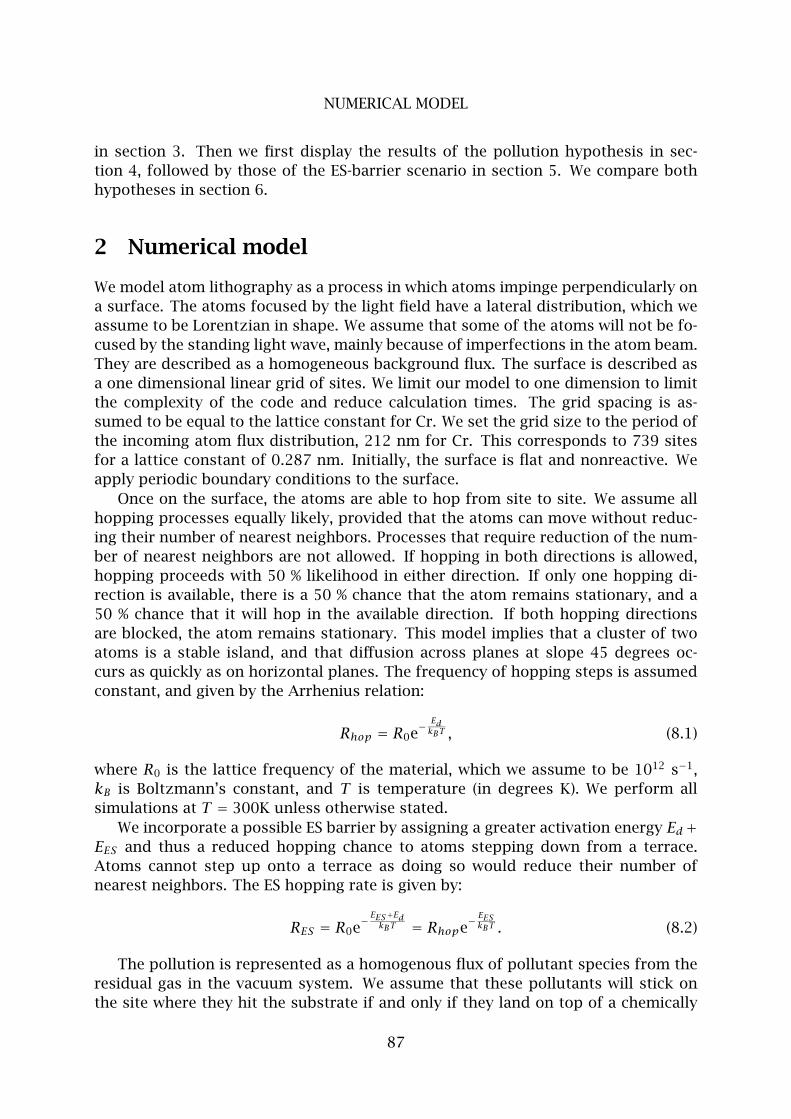
NUMERICAL MODEL
in section 3. Then we first display the results of the pollution hypothesis in sec-
tion 4, followed by those of the ES-barrier scenario in section 5. We compare both
hypotheses in section 6.
2 Numerical model
We model atom lithography as a process in which atoms impinge perpendicularly on
a surface. The atoms focused by the light field have a lateral distribution, which we
assume to be Lorentzian in shape. We assume that some of the atoms will not be fo-
cused by the standing light wave, mainly because of imperfections in the atom beam.
They are described as a homogeneous background flux. The surface is described as
a one dimensional linear grid of sites. We limit our model to one dimension to limit
the complexity of the code and reduce calculation times. The grid spacing is as-
sumed to be equal to the lattice constant for Cr. We set the grid size to the period of
the incoming atom flux distribution, 212 nm for Cr. This corresponds to 739 sites
for a lattice constant of 0.287 nm. Initially, the surface is flat and nonreactive. We
apply periodic boundary conditions to the surface.
Once on the surface, the atoms are able to hop from site to site. We assume all
hopping processes equally likely, provided that the atoms can move without reduc-
ing their number of nearest neighbors. Processes that require reduction of the num-
ber of nearest neighbors are not allowed. If hopping in both directions is allowed,
hopping proceeds with 50 % likelihood in either direction. If only one hopping di-
rection is available, there is a 50 % chance that the atom remains stationary, and a
50 % chance that it will hop in the available direction. If both hopping directions
are blocked, the atom remains stationary. This model implies that a cluster of two
atoms is a stable island, and that diffusion across planes at slope 45 degrees oc-
curs as quickly as on horizontal planes. The frequency of hopping steps is assumed
constant, and given by the Arrhenius relation:
Rhop = R0e− EdkBT , (8.1)
where R0 is the lattice frequency of the material, which we assume to be 1012 s−1,
kB is Boltzmann’s constant, and T is temperature (in degrees K). We perform all
simulations at T = 300K unless otherwise stated.
We incorporate a possible ES barrier by assigning a greater activation energy Ed+EES and thus a reduced hopping chance to atoms stepping down from a terrace.
Atoms cannot step up onto a terrace as doing so would reduce their number of
nearest neighbors. The ES hopping rate is given by:
RES = R0e− EES+EdkBT = Rhope
− EESkBT . (8.2)
The pollution is represented as a homogenous flux of pollutant species from the
residual gas in the vacuum system. We assume that these pollutants will stick on
the site where they hit the substrate if and only if they land on top of a chemically
87
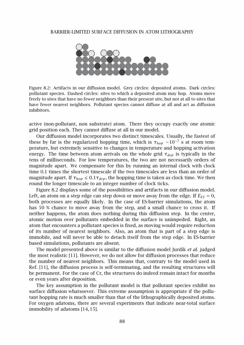
BARRIER-LIMITED SURFACE DIFFUSION IN ATOM LITHOGRAPHY
Figure 8.2: Artifacts in our diffusion model. Grey circles: deposited atoms. Dark circles:
pollutant species. Dashed circles: sites to which a deposited atom may hop. Atoms move
freely to sites that have no fewer neighbors than their present site, but not at all to sites that
have fewer nearest neighbors. Pollutant species cannot diffuse at all and act as diffusion
inhibitors.
active (non-pollutant, non substrate) atom. There they occupy exactly one atomic
grid position each. They cannot diffuse at all in our model.
Our diffusion model incorporates two distinct timescales. Usually, the fastest of
these by far is the regularized hopping time, which is τhop ∼10−7 s at room tem-
perature, but extremely sensitive to changes in temperature and hopping activation
energy. The time between atom arrivals on the whole grid τdep is typically in the
tens of milliseconds. For low temperatures, the two are not necessarily orders of
magnitude apart. We compensate for this by running an internal clock with clock
time 0.1 times the shortest timescale if the two timescales are less than an order of
magnitude apart. If τhop ≤ 0.1τdep, the hopping time is taken as clock time. We then
round the longer timescale to an integer number of clock ticks.
Figure 8.2 displays some of the possibilities and artifacts in our diffusion model.
Left, an atom on a step edge can step down or move away from the edge. If EES = 0,
both processes are equally likely. In the case of ES-barrier simulations, the atom
has 50 % chance to move away from the step, and a small chance to cross it. If
neither happens, the atom does nothing during this diffusion step. In the center,
atomic motion over pollutants embedded in the surface is unimpeded. Right, an
atom that encounters a pollutant species is fixed, as moving would require reduction
of its number of nearest neighbors. Also, an atom that is part of a step edge is
immobile, and will never be able to detach itself from the step edge. In ES-barrier
based simulations, pollutants are absent.
The model presented above is similar to the diffusion model Jurdık et al. judged
the most realistic [11]. However, we do not allow for diffusion processes that reduce
the number of nearest neighbors. This means that, contrary to the model used in
Ref. [11], the diffusion process is self-terminating, and the resulting structures will
be permanent. For the case of Cr, the structures do indeed remain intact for months
or even years after deposition.
The key assumption in the pollutant model is that pollutant species exhibit no
surface diffusion whatsoever. This extreme assumption is appropriate if the pollu-
tant hopping rate is much smaller than that of the lithographically deposited atoms.
For oxygen adatoms, there are several experiments that indicate near-total surface
immobility of adatoms [14,15].
88
SIMULATION PARAMETERS
3 Simulation parameters
We will now proceed to choose our parameters, being the atomic beam flux density
profile, the pollutant flux density, the deposition time, the hopping activation energy,
and the ES-barrier energy.
The atomic beam flux density profile is assumed to be a Lorentz distribution
on top of a homogeneous background, with a width equal to the values calculated
by Anderson et al.. We choose the contrast ratio (peak height to homogeneous back-
ground level) to be 3.5; our own simulations of focusing find that this is a reasonable
value in many cases. From the experimental data given by Anderson et al. [9], we de-
duce that the spatially averaged beam flux density was around 0.05 ML/s (1 ML =
1.21 × 10¹⁹ m−2). The deposition time is set at five minutes, as in the Anderson ex-
periment. The incoming flux distribution FWHM remains fixed at 20 nm when other
parameters are varied.
The diffusion activation energy Ed is the only free parameter in Eq. 8.1, and its
absolute value is unknown: the surface diffusion activation energy for Cr has never
been investigated experimentally. Only one calculation of its value is known to the
authors; Schindler [16] calculates a value of 0.22 eV for Cr[110]. In the same work,
he also finds values of 0.28 eV for Fe[110] and 0.47 eV for W[110]. Experimental
values for these systems are 0.225 eV and 0.87 eV, respectively. For other crystal
faces, the diffusion energies of Fe are consistently higher than those on the [110]
face. We conclude that for the structures under consideration, which are most likely
polycrystalline, the calculated value of 0.22 eV should be taken as a lower limit.
We choose to perform the simulations using an effective hopping activation energy
Ed = 0.30 eV.
We assume that the pollutant flux is constant and homogenous. We first make a
rudimentary estimate of the amount of pollution needed to explain the experimental
observations. The experimental structures are broadened by 20-30 nm with respect
to the incoming atom flux distribution. Per structure flank, the broadening is 10-
15 nm, or 35-50 sites. For a pollutant diffusion barrier, the distance to the nearest
pollutant adatom should be on the order of the diffusion length. The corresponding
amount of pollution is thus one in 35-50, or 2-3 %. In the absence of pollution, the
diffusion length has no fundamental limit. Thus, the influence of a small amount of
pollutants on the shape of the structures deposited could be immense.
The vacuum system was ion-pumped to a pressure of around 10−8 mbar [9],
which corresponds to a molecular background flux of around 2.5 × 10⁻³ ML/s. The
composition of the background gas is unknown. Literature indicates that the sticking
chance of oxygen on Cr is close to unity [17]. For nitrogen, the sticking coefficient is
similar [18]. Any water present can be assumed to stick as readily, and will therefore
also contribute O- or OH-groups to the surface. As there are at most two atoms per
molecule for these gases, we expect to find an effective chemically bonding pollutant
flux of up to 5×10⁻³ ML/s. The estimate above results in a pollutant flux of 1×10⁻³
to 1.5× 10⁻³ ML/s, well within this range. The model value will be determined from
the simulations.
The height of the ES-barrier also has never been determined experimentally for
89
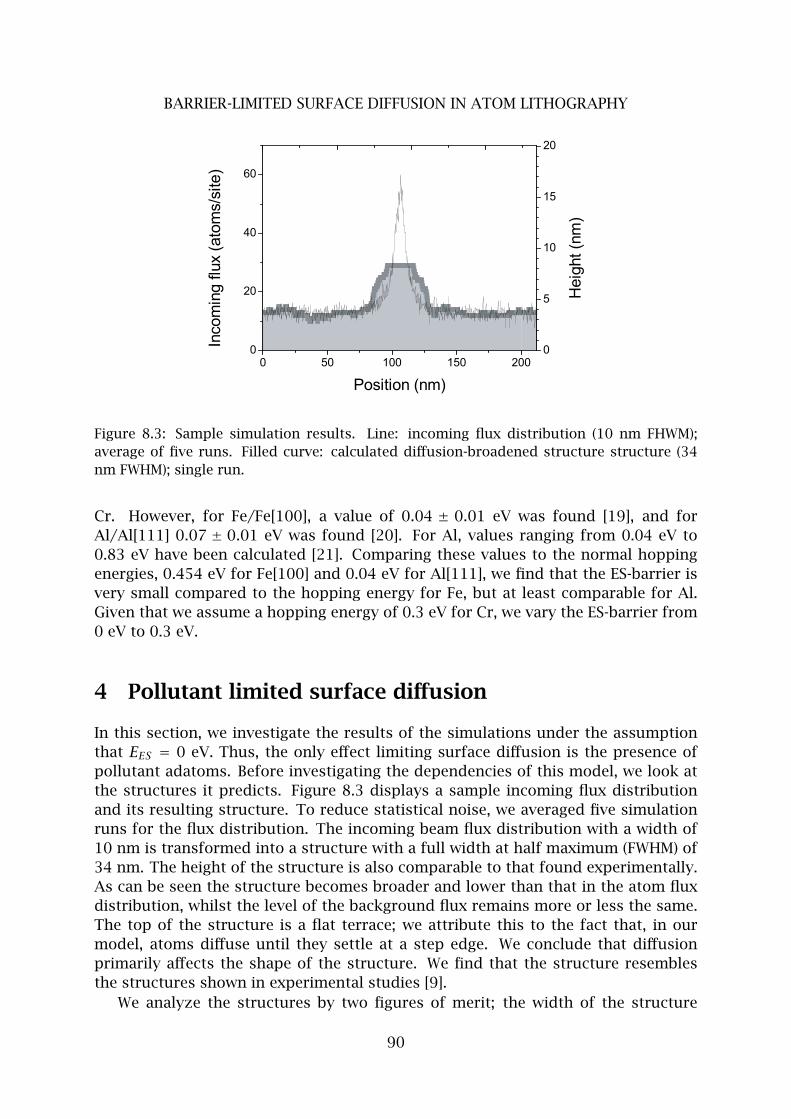
BARRIER-LIMITED SURFACE DIFFUSION IN ATOM LITHOGRAPHY
Figure 8.3: Sample simulation results. Line: incoming flux distribution (10 nm FHWM);
average of five runs. Filled curve: calculated diffusion-broadened structure structure (34
nm FWHM); single run.
Cr. However, for Fe/Fe[100], a value of 0.04 ± 0.01 eV was found [19], and for
Al/Al[111] 0.07 ± 0.01 eV was found [20]. For Al, values ranging from 0.04 eV to
0.83 eV have been calculated [21]. Comparing these values to the normal hopping
energies, 0.454 eV for Fe[100] and 0.04 eV for Al[111], we find that the ES-barrier is
very small compared to the hopping energy for Fe, but at least comparable for Al.
Given that we assume a hopping energy of 0.3 eV for Cr, we vary the ES-barrier from
0 eV to 0.3 eV.
4 Pollutant limited surface diffusion
In this section, we investigate the results of the simulations under the assumption
that EES = 0 eV. Thus, the only effect limiting surface diffusion is the presence of
pollutant adatoms. Before investigating the dependencies of this model, we look at
the structures it predicts. Figure 8.3 displays a sample incoming flux distribution
and its resulting structure. To reduce statistical noise, we averaged five simulation
runs for the flux distribution. The incoming beam flux distribution with a width of
10 nm is transformed into a structure with a full width at half maximum (FWHM) of
34 nm. The height of the structure is also comparable to that found experimentally.
As can be seen the structure becomes broader and lower than that in the atom flux
distribution, whilst the level of the background flux remains more or less the same.
The top of the structure is a flat terrace; we attribute this to the fact that, in our
model, atoms diffuse until they settle at a step edge. We conclude that diffusion
primarily affects the shape of the structure. We find that the structure resembles
the structures shown in experimental studies [9].
We analyze the structures by two figures of merit; the width of the structure
90
POLLUTANT LIMITED SURFACE DIFFUSION
and its contrast. As the structures are not Lorentzian in shape, we determine their
FWHM directly rather than from a curve fit. We define the contrast as the ratio of
the height difference between the structure top and the background and the height
difference between the background and substrate. We determine the background
level by taking the average height of the leftmost 50 grid points. All structure widths
and contrast ratios given from this point onwards are the averages of five simulation
runs, and all error bars indicate standard deviations of these distributions.
Figure 8.4 shows the resulting structure FWHM and contrast as a function of ef-
fective pollutant flux. At low fluxes, diffusion clearly causes a lot of broadening.
Also, the structure contrast is reduced strongly. These effects are very clearly sup-
pressed by increasing pollution. The width of the structures found matches that
found by Anderson et al. [9] for an effective pollutant flux of 2.0× 10⁻³ML/s. This is
well within the range predicted in section 3, and close to the rough estimate in the
introduction. We will use the value above throughout the remainder of this work.
The pollution model has no further free parameters.
4.1 Atom flux
We can now proceed to compare the results of our model to the experimental in-
vestigations of Anderson et al. [9]. That comparison is displayed at the bottom of
Fig. 8.5. The data points have been taken directly from their paper, and have been
plotted with the simulation results. We find very reasonable agreement between the
experiments and our simulations, with the two being within two standard deviations
of each other at all instances. Also shown is the incoming atom flux (dashed lines).
The diffusive broadening appears to be constant. This confirms our model of atoms
that can diffuse for a certain length until they encounter a pollutant atom. The
contrast of these structures is shown in the top half of Fig. 8.5. As can be seen, it
increases with increasing structure width. This supports our earlier conclusion that
the background height is not enhanced by the diffusion processes, but that instead
the peak area remains constant. The structure height then decreases as a result of
the broadening.
Varying the atom flux contrast ratio, we found no effect on the resulting struc-
ture widths; however, we did find that a greater atom flux contrast gives a greater
structure contrast, as shown in Fig. 8.6. This, too, favors the notion of the structure
being smeared out by diffusion more or less independently from the background.
4.2 Temperature
One peculiar experimental result was the lack of temperature dependence. The tem-
perature dependence of the results from our model is shown in Fig. 8.7. For a hop-
ping activation energy of 0.3 eV, we find no temperature dependence above 250 K.
Below this temperature, we find that the diffusion is limited by the low hopping rate
rather than by pollution. At higher temperatures, when the diffusion length of an
atom is determined by the distance to the nearest pollutant adatom or molecule,
diffusion becomes temperature independent. Lowering the activation energy lowers
91
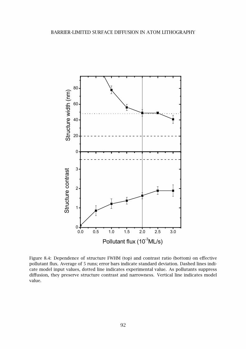
BARRIER-LIMITED SURFACE DIFFUSION IN ATOM LITHOGRAPHY
Figure 8.4: Dependence of structure FWHM (top) and contrast ratio (bottom) on effective
pollutant flux. Average of 5 runs; error bars indicate standard deviation. Dashed lines indi-
cate model input values, dotted line indicates experimental value. As pollutants suppress
diffusion, they preserve structure contrast and narrowness. Vertical line indicates model
value.
92
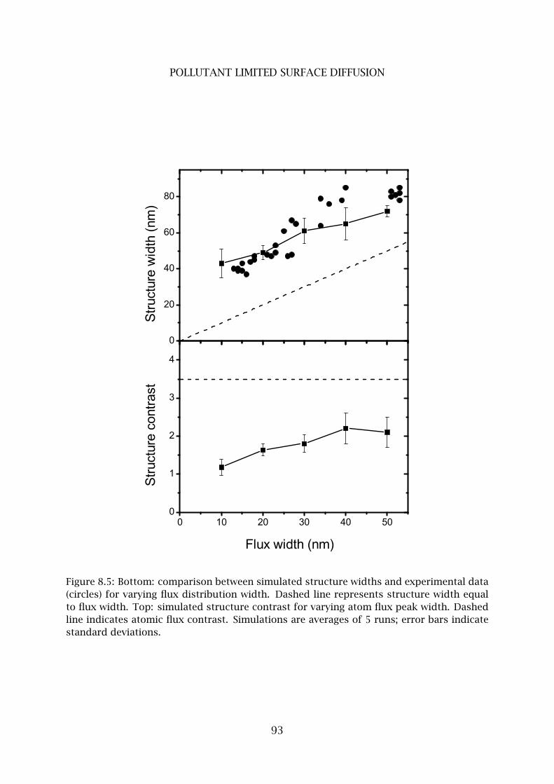
POLLUTANT LIMITED SURFACE DIFFUSION
Figure 8.5: Bottom: comparison between simulated structure widths and experimental data
(circles) for varying flux distribution width. Dashed line represents structure width equal
to flux width. Top: simulated structure contrast for varying atom flux peak width. Dashed
line indicates atomic flux contrast. Simulations are averages of 5 runs; error bars indicate
standard deviations.
93
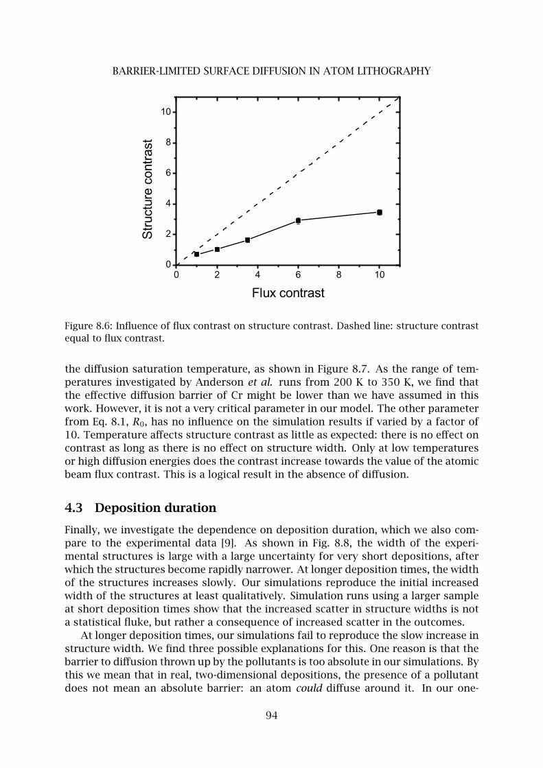
BARRIER-LIMITED SURFACE DIFFUSION IN ATOM LITHOGRAPHY
Figure 8.6: Influence of flux contrast on structure contrast. Dashed line: structure contrast
equal to flux contrast.
the diffusion saturation temperature, as shown in Figure 8.7. As the range of tem-
peratures investigated by Anderson et al. runs from 200 K to 350 K, we find that
the effective diffusion barrier of Cr might be lower than we have assumed in this
work. However, it is not a very critical parameter in our model. The other parameter
from Eq. 8.1, R0, has no influence on the simulation results if varied by a factor of
10. Temperature affects structure contrast as little as expected: there is no effect on
contrast as long as there is no effect on structure width. Only at low temperatures
or high diffusion energies does the contrast increase towards the value of the atomic
beam flux contrast. This is a logical result in the absence of diffusion.
4.3 Deposition duration
Finally, we investigate the dependence on deposition duration, which we also com-
pare to the experimental data [9]. As shown in Fig. 8.8, the width of the experi-
mental structures is large with a large uncertainty for very short depositions, after
which the structures become rapidly narrower. At longer deposition times, the width
of the structures increases slowly. Our simulations reproduce the initial increased
width of the structures at least qualitatively. Simulation runs using a larger sample
at short deposition times show that the increased scatter in structure widths is not
a statistical fluke, but rather a consequence of increased scatter in the outcomes.
At longer deposition times, our simulations fail to reproduce the slow increase in
structure width. We find three possible explanations for this. One reason is that the
barrier to diffusion thrown up by the pollutants is too absolute in our simulations. By
this we mean that in real, two-dimensional depositions, the presence of a pollutant
does not mean an absolute barrier: an atom could diffuse around it. In our one-
94
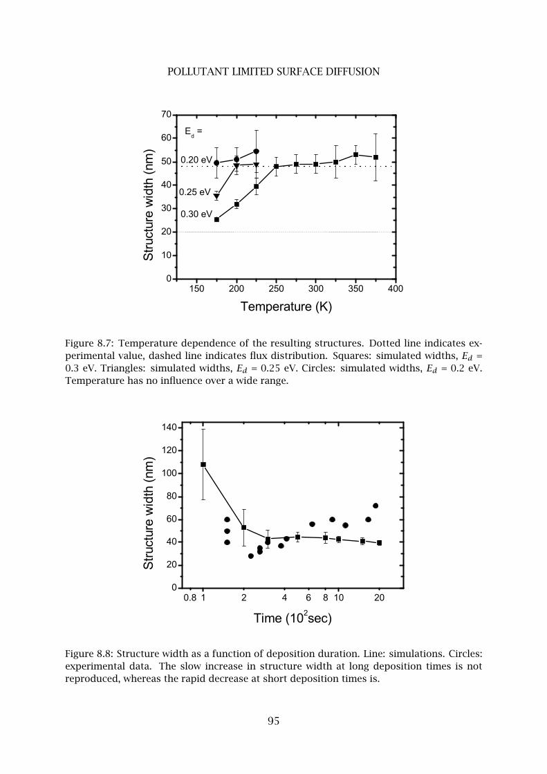
POLLUTANT LIMITED SURFACE DIFFUSION
Figure 8.7: Temperature dependence of the resulting structures. Dotted line indicates ex-
perimental value, dashed line indicates flux distribution. Squares: simulated widths, Ed =
0.3 eV. Triangles: simulated widths, Ed = 0.25 eV. Circles: simulated widths, Ed = 0.2 eV.
Temperature has no influence over a wide range.
Figure 8.8: Structure width as a function of deposition duration. Line: simulations. Circles:
experimental data. The slow increase in structure width at long deposition times is not
reproduced, whereas the rapid decrease at short deposition times is.
95
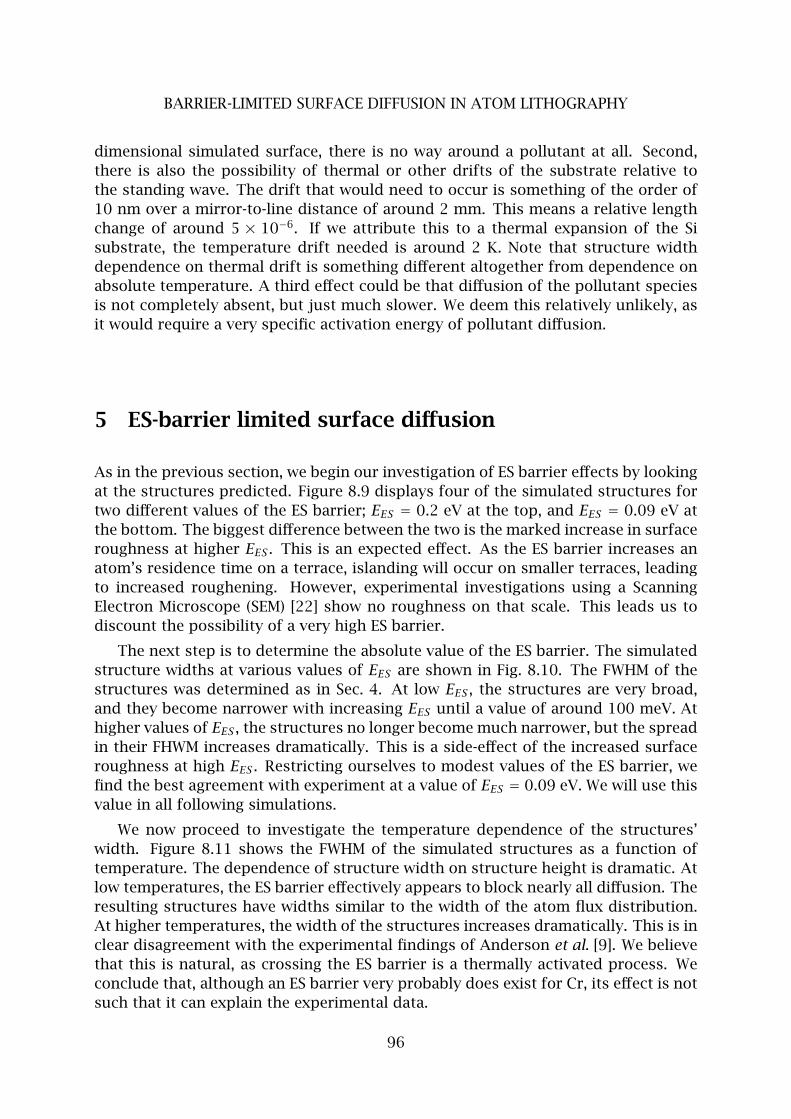
BARRIER-LIMITED SURFACE DIFFUSION IN ATOM LITHOGRAPHY
dimensional simulated surface, there is no way around a pollutant at all. Second,
there is also the possibility of thermal or other drifts of the substrate relative to
the standing wave. The drift that would need to occur is something of the order of
10 nm over a mirror-to-line distance of around 2 mm. This means a relative length
change of around 5 × 10⁻⁶. If we attribute this to a thermal expansion of the Si
substrate, the temperature drift needed is around 2 K. Note that structure width
dependence on thermal drift is something different altogether from dependence on
absolute temperature. A third effect could be that diffusion of the pollutant species
is not completely absent, but just much slower. We deem this relatively unlikely, as
it would require a very specific activation energy of pollutant diffusion.
5 ES-barrier limited surface diffusion
As in the previous section, we begin our investigation of ES barrier effects by looking
at the structures predicted. Figure 8.9 displays four of the simulated structures for
two different values of the ES barrier; EES = 0.2 eV at the top, and EES = 0.09 eV at
the bottom. The biggest difference between the two is the marked increase in surface
roughness at higher EES . This is an expected effect. As the ES barrier increases an
atom’s residence time on a terrace, islanding will occur on smaller terraces, leading
to increased roughening. However, experimental investigations using a Scanning
Electron Microscope (SEM) [22] show no roughness on that scale. This leads us to
discount the possibility of a very high ES barrier.
The next step is to determine the absolute value of the ES barrier. The simulated
structure widths at various values of EES are shown in Fig. 8.10. The FWHM of the
structures was determined as in Sec. 4. At low EES , the structures are very broad,
and they become narrower with increasing EES until a value of around 100 meV. At
higher values of EES , the structures no longer become much narrower, but the spread
in their FHWM increases dramatically. This is a side-effect of the increased surface
roughness at high EES . Restricting ourselves to modest values of the ES barrier, we
find the best agreement with experiment at a value of EES = 0.09 eV. We will use this
value in all following simulations.
We now proceed to investigate the temperature dependence of the structures’
width. Figure 8.11 shows the FWHM of the simulated structures as a function of
temperature. The dependence of structure width on structure height is dramatic. At
low temperatures, the ES barrier effectively appears to block nearly all diffusion. The
resulting structures have widths similar to the width of the atom flux distribution.
At higher temperatures, the width of the structures increases dramatically. This is in
clear disagreement with the experimental findings of Anderson et al. [9]. We believe
that this is natural, as crossing the ES barrier is a thermally activated process. We
conclude that, although an ES barrier very probably does exist for Cr, its effect is not
such that it can explain the experimental data.
96
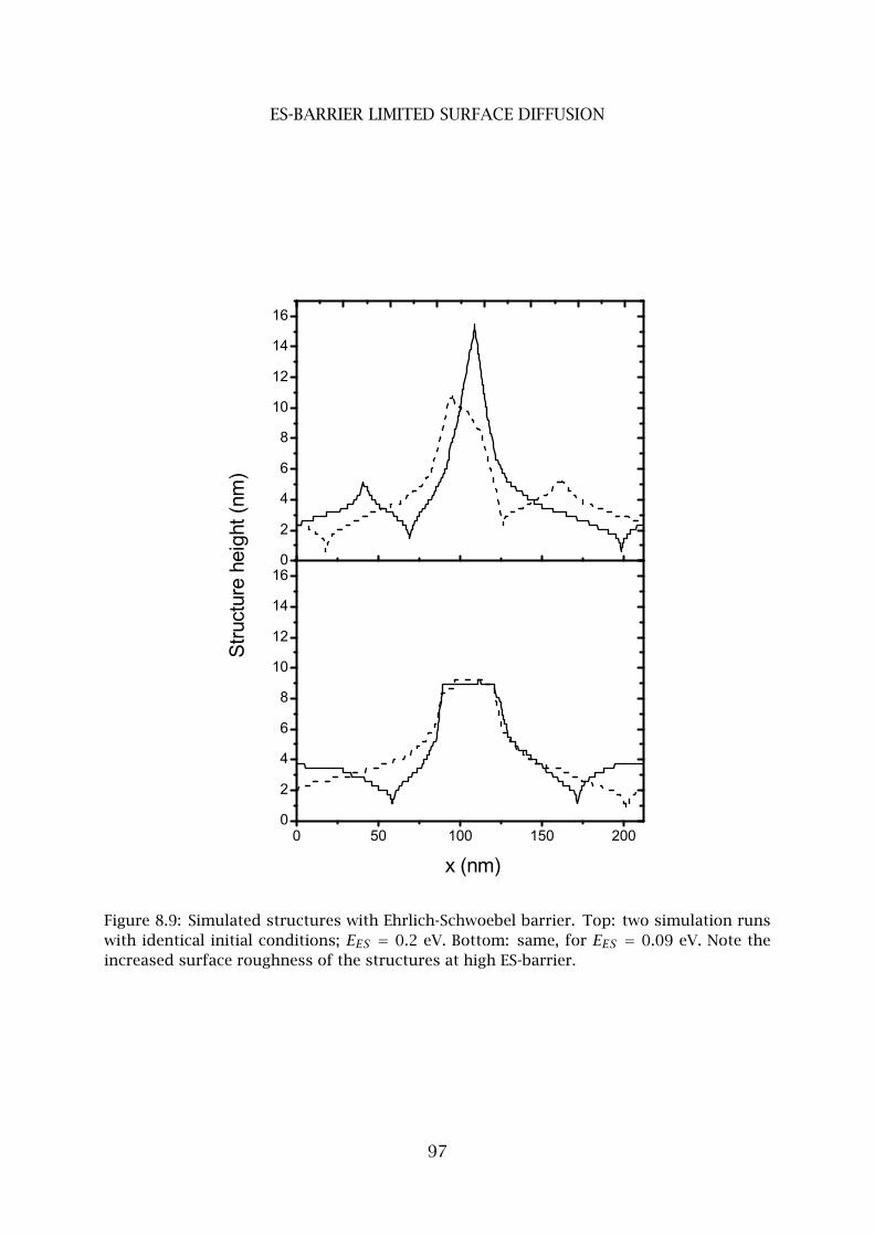
ES-BARRIER LIMITED SURFACE DIFFUSION
Figure 8.9: Simulated structures with Ehrlich-Schwoebel barrier. Top: two simulation runs
with identical initial conditions; EES = 0.2 eV. Bottom: same, for EES = 0.09 eV. Note the
increased surface roughness of the structures at high ES-barrier.
97
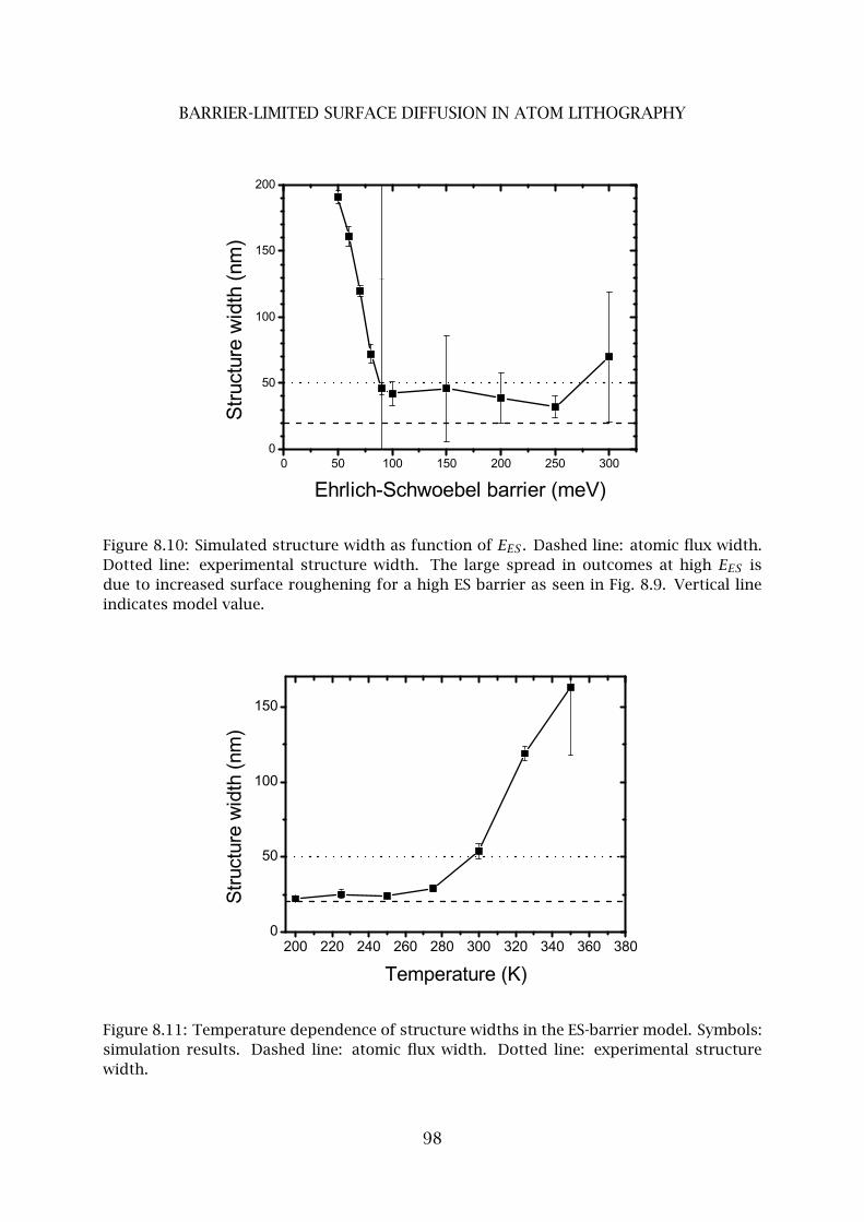
BARRIER-LIMITED SURFACE DIFFUSION IN ATOM LITHOGRAPHY
Figure 8.10: Simulated structure width as function of EES . Dashed line: atomic flux width.
Dotted line: experimental structure width. The large spread in outcomes at high EES is
due to increased surface roughening for a high ES barrier as seen in Fig. 8.9. Vertical line
indicates model value.
Figure 8.11: Temperature dependence of structure widths in the ES-barrier model. Symbols:
simulation results. Dashed line: atomic flux width. Dotted line: experimental structure
width.
98
CONCLUSIONS
6 Conclusions
We have modelled structure broadening by atomic diffusion in atom lithography. In
our models, we have assumed that atomic diffusion occurs as a thermally activated
process that is frustrated by some kind of barrier. We explore two different possible
causes for this barrier. One mechanism is that pollutant adatoms from the vacuum
background limit surface diffusion by posing a physical barrier. The alternative is
that surface diffusion is limited by an ES barrier that is inherent in surface diffusion.
We have performed KMC simulations of both limiting mechanisms.
The results of the pollutant-based simulation match the experimental results [9]
very well. The barrier imposed by the pollutant species effectively suppresses the
temperature dependence of the structure broadening. The only incongruence be-
tween our model and the experimental results is in the deposition time dependence
of the structure widths. At longer deposition times, our model fails to predict the
observed increase in structure broadening. This could be due to the one-dimensional
nature of our simulations or to experimental drifts. A third possibility is that it is
due to one of the many possible diffusion processes we have neglected. The ES-
barrier utterly fails to reproduce the experimental lack of temperature dependence,
and hence we believe that it is not the dominant factor in surface diffusion of Cr.
The veracity of the claims we make here would be interesting to test experimen-
tally. This would not be very difficult as all one has to do is to introduce a controlled
leak in the deposition vacuum. Furthermore, the pollutant barrier might be exploited
to tune structure widths in atom lithography. The diffusion model could be further
refined by the inclusion of several slower diffusion processes, such as, for instance,
step edge detachment and pollutant adatom diffusion.
This work is financially supported by the Dutch Foundation for Fundamental
Research on Matter (FOM). We wish to thank M. K. Oberthaler and D. Jurgens for
useful discussions.
References
[1] H. Metcalf and P. van der Straten, Laser Cooling and Trapping (Springer, New York,
1999)
[2] D. Meschede and H. Metcalf, J. Phys. D: Appl. Phys., 36, R17-R38 (2003)
[3] Th. Schulze, T. Muther, D. Jurgens, B. Brezger, M. K. Oberthaler, T. Pfau, and J. Mlynek,
Appl. Phys. Lett. 78, 1781-1783 (2001)
[4] R. E. Behringer, V. Natarajan, and G. Timp, Appl. Phys. Lett. 68, 1034-1036 (1996)
[5] G. Timp, R. E. Behringer, D. M. Tennant, J. E. Cunningham, M. Prentiss, and K. K.
Berggren, Phys. Rev. Lett. 69, 1636-1639 (1992)
[6] J. J. McClelland, R. E. Scholten, E. C. Palm, and R. J. Celotta, Science 262, 877 (1993)
[7] R. W. McGowan, D. M. Giltner, and S. A. Lee, Opt. Lett. 20, 2535-2537 (1995)
99
BARRIER-LIMITED SURFACE DIFFUSION IN ATOM LITHOGRAPHY
[8] E. te Sligte, R. C. M. Bosch, B. Smeets, P. van der Straten, H. C. W. Beijerinck, and K. A.
H. van Leeuwen, Proc. Natl. Acad. Sci. 99, 6509-6513 (2002)
[9] W. R. Anderson, C. C. Bradley, J. J. McClelland, and R. J. Celotta, Phys. Rev. A 59, 2476-
2485 (1999)
[10] R. E. Behringer, V. Natarajan, and G. Timp, Appl. Surf. Sci. 104/105, 291-296 (1996)
[11] E. Jurdık, Th. Rasing, H. van Kempen, C. C. Bradley, and J. J. McClelland, Phys. Rev. B
60, 1543-1546 (1999)
[12] R. M. Bradley, A. Eschmann, and S. A. Lee, Journ. Appl. Phys. 88, 3316-3322 (2000)
[13] A. Pimpinelli and J. Villain, Physics of Crystal Growth, Cambridge University Press,
Cambridge (1998)
[14] H. Brune, J. Wintterlin, R. J. Behm, and G. Ertl, Phys. Rev. Lett. 68, 624-626 (1992)
[15] R. X. Ynzunza, R. Denecke, F. J. Palomares, J. Morais, E. D. Tober, Z. Wang, F. J. Garcıa
de Abajo, J. Liesegang, Z. Hussain, M. A. van Hove, and C. S. Fadley, Surf. Sci. 459,
69-92 (2000)
[16] A. C. Schindler, PhD thesis, Gerhard-Mercator-Universitat, Duisburg (1999)
[17] G. Gewinner, J. C. Peruchetti, A. Jaegle, and A. Kalt, Surf. Sci. 78, 439-458 (1978)
[18] J. E. Simpkins and P. Mioduszewski, J. Vac. Sci. Tech. 20, 1321 (1982)
[19] J. G. Amar and F. Family, Thin Solid Films 272, 208-222 (1996)
[20] R. Stumpf and M. Scheffler, Phys. Rev. Lett. 72, 254-257 (1993)
[21] S. J. Liu, H. Huang, and C. H. Woo, Appl. Phys. Lett., 80, 3295-3297 (2002); M. G. Lagally
and Z. Zhang, Nature, 417, 907-908 (2002)
[22] J. J. McClelland, R. Gupta, Z. J. Jabbour, and R. J. Celotta, Aust. J. Phys., 49 555-565
(1996)
100
SUMMARY
Summary
Atom lithography is a technique in which a light field is used to pattern an atomic
beam. This patterned flux is then deposited onto a substrate, resulting in a nanos-
tructured thin film. The smallest structures that have been made thus far using this
technique are around 30 nm wide. This thesis investigates the technique, expanding
its possibilities.
The work-horse for the development of atom lithography has been Cr, as this
transition metal atom has a closed transition in a wavelength range that is accessible
to dye lasers. We extend the technique to Fe, the first ferromagnetic element to
be used for atom lithography. The setup that was used to do this experiment is
described, along with its critical design parameters.
We present nanostructures that are typically 50 nm wide, and up to 4 nm high.
The spacing between the nanolines is 186.05 nm. The nanostructure profile is com-
pared to that of a simulated deposition process, and found to match. To the authors’
knowledge, this is the first demonstration of direct write atom lithography without
laser cooling.
A preliminary incursion into the magnetic properties of the nanostructures de-
posited is presented. In addition to giving an overview of the general ferromagnetic
properties that might be expected, a deeper investigation of the magnetic anisotropy
of the nanostructures deposited in this experiment is given.
Novel resonant light masks are used in an experiment performed at the Univer-
sity of Konstanz (Germany). These light masks, using exactly instead of nearly reso-
nant light, reveal some intriguing quantum mechanical effects. The most important
of these features is the possibility to place structures closer together – at quarter
wavelength spacings rather than half-wavelength intervals.
Finally, the influence of surface diffusion on the structures obtained in an atom
lithography experiment is investigated using kinetic Monte Carlo simulations. Sev-
eral diffusion limiting effects are investigated; the influence of small amounts of
residual reactive background gas is found to describe the experimental observa-
tions.
101

SAMENVATTING
Samenvatting
Atoomlithografie is een techniek waarbij een lichtveld wordt gebruikt om een pa-
troon aan te brengen in een atoombundel. Deze gemoduleerde flux slaat vervolgens
neer op een substraat; het resultaat is een genanostructureerde dunne film. De
kleinste structuren die tot nu toe op deze wijze zijn gemaakt zijn lijntjes van 30 nm
breed. In dit proefschrift wordt deze experimentele techniek onderzocht en haar
mogelijkheden uitgebreid.
Het werkpaard in de ontwikkeling van de atoomlithografie is tot nu toe Cr ge-
weest, een overgangsmetaal waarvan de atomen een gesloten overgang hebben in
een golflengtebereik dat voor dye-lasers toegankelijk is. Wij breiden de techniek
uit naar Fe, het eerste ferromagnetische element dat voor atoomlithografie gebruikt
wordt. De opstelling die voor dit experiment is gebruikt wordt beschreven, met de
kritieke ontwerp-parameters.
Als experimenteel resultaat worden nanolijnen getoond die typisch 50 nm breed
zijn, en tot 4 nm hoog. De periode van de structuren is 186.05 nm. Het profiel van
de structuren wordt vergeleken met dat wat voortkomt uit een simulatie van het de-
positieproces; beiden stemmen overeen. Voor zover op dit moment aan de auteur
bekend is dit de eerste toepassing van depositie-atoomlithografie zonder laserkoe-
ling.
Een eerste theoretische verkenning van de magnetische eigenschappen van de
nanostructuren wordt gepresenteerd. Naast een overzicht van de algemene ferro-
magnetische eigenschappen die verwacht kunnen worden, wordt ook een dieper on-
derzoek naar de magnetische anisotropie van de nanostructuren uit dit experiment
gegeven.
Vernieuwende lichtmaskers worden gebruikt in een experiment dat is uitgevoerd
aan de Universiteit van Konstanz (Duitsland). Deze lichtmaskers, met exact re-
sonant in plaats van bijna resonant licht, brengen enkele fascinerende quantum-
mechanische effecten aan het licht. Het belangrijkste effect is dat het hierdoor mo-
gelijk wordt structuren dichter bij elkaar te plaatsen – met een periode van een kwart
golflengte in plaats van een halve golflengte.
Tenslotte wordt de invloed van oppervlaktediffusie op de structuren onderzocht
met behulp van kinetische Monte Carlo simulaties. Verschillende diffusie-effecten
worden onderzocht; de invloed van kleine hoeveelheden reactief achtergrondgas
blijkt de experimentele observaties te beschrijven.
102
DANKWOORD
Dankwoord
Hoewel een proefschrift veel eenzame arbeid vereist, heb ik bij de totstandkoming
ervan ook veel gehad aan anderen; hen wil ik hier graag bedanken.
In de eerste plaats natuurlijk mijn eerste promotor Ton van Leeuwen, voor ontel-
bare commentaren, tips en adviezen, en natuurlijk de ontdekking van Sambal Badjak.
Daarnaast mijn tweede promotor Herman Beijerinck, zonder wie ik waarschijnlijk
nooit aan dit project zou zijn begonnen, en zonder wiens noodgedwongen inzet ik
misschien ook niet op tijd de eindstreep zou hebben gehaald.
In het lab ben ik mijn collega Bart Smeets veel dank verschuldigd; voor een be-
langrijk deel dankzij zijn soms haast magische verstandhouding met de laser bevat
dit proefschrift ook experimentele resultaten. Ook afstudeerders Richard van der
Stam en Rodolf Herfst zijn van grote waarde geweest. Met Roel Bosch heb ik in mijn
eerste half jaar nog zeer prettig gewerkt aan een destijds zeer frustrerende opstel-
ling. De technische ondersteuning van Louis van Moll en Jolanda van de Ven is vier
jaar lang telkens weer van onschatbare waarde gebleken. Mijn collega’s in de groep
wil ik graag bedanken voor de goeie werksfeer.
I would also like to thank everybody I worked with at the University of Kon-
stanz for a splendid time. Especially, I would like to thank Dirk Jurgens and Markus
Oberthaler for a fruitful, interesting, and very friendly cooperation.
Tenslotte ben ik Sigrid erg dankbaar voor haar morele steun, warmte en hulp-
vaardigheid, vooral op onmogelijke en/of onverwachte tijdstippen.
103
DANKWOORD
Curriculum Vitae
3 september 1977 Geboren te Gouda
1988-1994 Gymnasium,
Lorentz Lyceum te Eindhoven
1994-2001 Studie Technische Natuurkunde,
Technische Universiteit Eindhoven,
doctoraal examen april 2001.
2001-2005 Assistent-In-Opleiding,
Experimentele Atoomfysica en Quantumelektronica,
Faculteit Technische Natuurkunde,
Technische Universiteit Eindhoven
104