audio engineering society convention paper - tc … · audio engineering society convention paper...
TRANSCRIPT

Audio Engineering Society Convention Paper
Presented at the 116th Convention 2004 May 8–11 Berlin, Germany
This convention paper has been reproduced from the author's advance manuscript, without editing, corrections, or consideration by the Review Board. The AES takes no responsibility for the contents. Additional papers may be obtained by sending request and remittance to Audio Engineering Society, 60 East 42nd Street, New York, New York 10165-2520, USA; also see www.aes.org. All rights reserved. Reproduction of this paper, or any portion thereof, is not permitted without direct permission from the Journal of the Audio Engineering Society.
Plug and Play? An investigation into problems and solutions of digital audio networks
Christian G. Frandsen1 and Morten Lave2
1 R&D, TC Electronic A/S, 8240 Risskov, Denmark [email protected]
2 TC Applied Technologies Ltd., Markham, ON, LR3 2Z5, Canada [email protected]
ABSTRACT
It is a challenge to predict fault tolerance of the total system using point-to-point digital audio interfaces to build complex routing structures. In real life, digital interfacing is therefore still considered less robust than analog. This paper provides a systematic investigation of factors determining reliability in a number of widely used professional audio and synchronisation interfaces such as AES3, SPDIF, ADAT, TDIF and Word Clock. Electrical characteris-tics, phase-offset and tolerance to offset, intrinsic jitter and tolerance to jitter, and sample rate precision have been tested. Additionally, compliancy with standards has been evaluated. Finally, a discussion how these problems can be dealt with followed by specific thoughts about the next generation of interfaces will be presented with examples.
1. INTRODUCTION
Even experienced audio engineers have difficulty under-standing why the same equipment interfaced digitally using the same connections can behave differently from day to day. What is the source of this inconsistency, and why doesn't interfacing standards take care of it?
Since the mid ’80’s when point-to-point interfaces for transporting digital audio were introduced, we have seen several types being added and now they form an indis-tinctive picture. Most of the new types have been added by manufacturers and some of the types have been standardised later e.g. by IEC. The interface types
typically differ by transport media, number of audio channels, supported sample rates, supported word lengths and connector type. Some types are related to typical working areas: For example the ADAT interface [7], which was introduced by Alesis on stand-alone 8 channel digital tape recorders. The ADAT interface is now widely used on computer interface cards due to its high channel density and small outline (8 channels in a small optical connector).
The indistinctive picture of digital interfacing shows when connecting a digital audio workstation (DAW) to external effects-machines. The DAW might have an interface card featuring an ADAT interface and the ex-ternal equipment might feature AES [1] and SPDIF (So-ny/Philips Digital Interface) [2]. A format converter is

Frandsen and Lave Plug and Play? Digital network investigation
AES 116th Convention, Berlin, Germany, 2004 May 8–11 Page 2 of 31
needed and furthermore there might be a wish for syn-chronising all products to a common source like Word Clock (WC), which is often referred to as a house clock. A simple setup fairly quickly becomes complex this way.
It might be due to the complexity and potential deficien-cy of such systems that analog interfacing is still consi-dered more robust than digital. Real life experience shows us that the connections are occasionally not “plug and play” - which would be the ideal situation. End-users find themselves fighting against problems like:
• Problems when synchronizing audio to picture
• Products that should but cannot communicate with each other in both general and specific setups
• Unfortunate digital receiver lock-up strategy in pro-ducts
• Problems when changing sample rate
• Insufficient validation of audio sources before lock-ing to them
• Unfortunate behaviour when losing lock
• Inputs that stop working when the product is clock master
How much time is spent on finding work-arounds instead of being creative in the music studio?
It is unfortunate that point-to-point interfaces seem to have significant deficiencies 20 years after their intro-duction to the market. Furthermore, it is unfortunate that the end-users therefore not fully exploit the advantages of the digital data transfer. These advantages are e.g. no induced hum and noise across the wire and no distortion in the interface front-end.
Are the problems overwhelming or too complex for the manufacturers to address? Are the standards too few or are they inadequate? Do the end-users have too little knowledge about the problems - and not enough to be self-reliant?
The shift from analog to digital connections has taken place with different speed in different areas. Project studios and conventional studios have moved towards digital setups mainly over the last decade. In the Public Address and the broadcast industry the shift is happe-ning these years. The reason for the PA and the broad-
cast industry to only reluctantly embrace the new tech-nology might be the discussed deficiencies on digital interfacing, which those industries are potentially extre-mely sensitive to.
Currently, the audio industry is facing a shift from point-to-point interfaces to intelligent networks. One advantage is that various data and not solely audio is transferred between the products. This data could be remote control information to the products and informa-tion for configuring the network. Because all products on the network are using the same interface system there should be a similar way of setting up the products. Furthermore, the way of working with products on the network will become comparable if not identical. Typi-cally, signal routing between products on the network is very flexible and configurable, which is also a big ad-vantage.
This amount of complexity represents a challenge to the audio industry. Is it ready to accept that challenge given the deficiencies still present on the conventional simple point-to-point connections?
This paper will examine the potential deficiencies of the conventional point-to-point audio and synchronisation interfaces. These include AES3, SPDIF, ADAT, TDIF [8] and Word Clock. We will focus on a number of parameters including both electrical and timing beha-viour. The results are compared to the standards avail-able, and the deficiencies are evaluated. This paper will only examine professional audio equipment but the fin-dings are discussed with respect to consumer equipment as well.
2. METHODS
In order to investigate the different interfaces, we examined 22 products on the market. The samples had different focus areas:
• 4 mixing consoles
• 7 effects-processors
• 3 AD and DA-converters
• 2 digital format converters
• 2 computer interfaces
• 3 stand-alone hard disk recorders
• 1 speaker set

Frandsen and Lave Plug and Play? Digital network investigation
AES 116th Convention, Berlin, Germany, 2004 May 8–11 Page 3 of 31
15 different manufacturers made the samples, the samp-les were released from 1996 to 2003 and they were pri-ced approximately from 400 to 18,000 USD.
The number of examined interfaces amounted to:
• 12 AES instances
• 10 SPDIF instances
• 15 ADAT instances
• 5 TDIF instances
• 17 Word Clock instances
The interfaces were tested with respect to a number of parameters including both electrical and timing beha-viour.
Electrical parameters consisted of:
• Output level (loaded)
• Input level sensitivity
• Impedances
• Rise-time
• High-pass filter corner frequency (ability to hold the signal level limited due to an AC coupling design)
• Ringing (overshoot peak-peak)
Timing parameters consisted of:
• Deviation of internal sample rate
• Intrinsic jitter in both clock master and clock slave mode
• Input-output phase offset
• Phase tolerance (data reading point or slip sample point) on inputs
• Jitter tolerance on inputs
• Input-output jitter transfer function (JTF)
Phase offset was also tested across interfaces e.g. AES output phase when the product clock slaved to WC input. Similarly, phase tolerance was tested across
interfaces e.g. phase tolerance on AES input when the product clock slaved to WC input.
Not all parameters were tested on all interfaces e.g. electrical parameters on the optical ADAT interface. Not all products provided opportunity to test all para-meters e.g. when a product could only be clock master there was no JTF to test.
All measurements were performed at 48 kHz unless otherwise noted.
An Audio Precision System 2 Cascade (AP) was used as the general measurement tool. For verification, a Tek-tronix TDS 220 scope was used to monitor e.g. the off-set parameters. A HP function generator 33120A was used to generate special signals for WC and TDIF inputs. In order to test ADAT and TDIF interfaces an RME ADI-8 DD digital format converter was connected between the AP AES interface and the interface on the product under test (Device Under Test, DUT).
Audio Precision has provided a number of test configu-ration files [4] for the System 2 Cascade measurement system. The files were used during the investigation.
2.1. Electrical parameters
The AP was used to measure all the electrical interface parameters for AES and SPDIF. The output levels were tested using different loads: AES 110 Ω, SPDIF 75 Ω and WC 75 Ω. On TDIF only the LR-clk was examined and the output load was 56 Ω.
For WC and TDIF input sensitivity test the HP function generator was used to find the minimum level that the product would lock to. The DC offset was adjusted so that the signal was always 0 to x V.
WC and TDIF rise time and ringing was measured on the oscilloscope.
The interface output level parameter was measured disregarding any potential droop (voltage droop on the horizontal waveform part due to an AC coupling de-sign). This means that the full peak-peak voltage was measured.

Frandsen and Lave Plug and Play? Digital network investigation
AES 116th Convention, Berlin, Germany, 2004 May 8–11 Page 4 of 31
Figure 1 Example of an ADAT test setup using RME
ADI8-DD to convert between AES and ADAT. Oscilloscope for verification and phase measurements.
Reference values for the electrical parameters specified in the standards are shown in Table 1. These are the values used to evaluate the compliance with the standards on the individual interfaces.
2.2. Timing parameters
As with the electrical parameters the AP was used to generate and measure the timing parameters.
Intrinsic jitter was measured with the product being clock master and clock slave to a specific interface type respectively.
Input-output phase offset was measured using oscillo-scope as shown in Figure 1.
Phase tolerance was measured with oscilloscope using the AP to generate the offset between its main output and its reference inputs and outputs. 1 UI peak (163 ns peak @ 48 kHz) of 100 Hz sine wave jitter was applied in that test to cross the receivers data reading point per-sistently. Receivers featuring hysteresis was examined using higher jitter levels (a maximum of 12.75 UI peak jitter is possible with the AP). It was verified that re-ceivers being exposed to this amount of jitter remained locked through the phase tolerance test.
The step size, in which the phase offset can be set in the AP, is 0.5 UI. The combination of the step size and the applied level of jitter meant that the receivers could have hysteresis of up to 2 UI and still would be regarded as hysteresis-free in this paper.
Jitter tolerance was tested using a number of sine wave jitter frequencies and wide band jitter and compared to the tolerance template from AES3 [1]. The mea-surement unit is UI because the AES tolerance template uses UI so for comparison reasons that unit was also used for testing ADAT and TDIF inputs. The UI defini-tion, which originates from the AES standard, is 128 UI per audio sample period e.g.
1 UI = 1/(48000 x 128) = 163 ns @ 48 kHz.
The jitter tolerance on WC inputs was only tested roughly (at 100 Hz jitter frequency) because the AP is unable to output jitter on its WC reference output sepa-rately i.e. there is also jitter on the main audio output. This meant that the interface (e.g. AES) used for veri-fication of audio-through during this test received the same amount of jitter and this interface typically lost lock before the WC interface did.
The jitter transfer function JTF was examined by
AP
AES out
AES in
WC out
RME DUT
AES ADAT
ADAT AES ADAT out
ADAT in
WC in
Output characteristics Impedance Output level
Input level tolerance
Rise time HPF corner Input Output
Standard
Vpp mVpp ns kHz Ω AES standard 2-7 <200 5-30 <100 88-132 88-132 60958 standard 0.4 - 0.6 <200 <65 <100 71-79 71-79
TDIF standard 2-3 N/A N/A N/A >1k5 45-67 ADAT N/A N/A N/A N/A N/A N/A WC, AES11-2003 <0.4/>2.4 V <0.4/>2.4 V N/A N/A N/A N/A
Table 1 Standards for the electrical parameters.

Frandsen and Lave Plug and Play? Digital network investigation
AES 116th Convention, Berlin, Germany, 2004 May 8–11 Page 5 of 31
applying a specific amount of sine wave jitter corres-ponding to the jitter level which an AES receiver must tolerate at all jitter frequencies. The AP extracts the returned jitter level as a function of the frequency and plots the transfer function.
Intrinsic jitter measurements on the ADAT and TDIF interface were affected by the performance of the RME (the AES-ADAT-TDIF format converter). In AES- ADAT conversion the RME adds 2.3 and 2.4 ns peak when 700 Hz and 50 Hz high-pass filtered (HPF) respectively and in AES-TDIF conversion it adds 3 and 3.5 ns peak respectively. There is a general upper corner frequency of 100 kHz on the jitter level measurement.
The RME affected the jitter level applied from the AP at the jitter frequencies used during the jitter tolerance test on ADAT and TDIF inputs insignificantly – the appro-ximate 0 dB of jitter gain through the RME was verified on oscilloscope.
The JTF on the RME had sufficiently high low-pass filter corner frequency and little peaking to not affect the measurements made on the chosen products except for a few cases where the JTF results were omitted.
Comment on phase measurements
All the results for phase offset and phase tolerance were found with respect to the phase definition in Figure 2. 0% phase reference is at the beginning of the X/Z-preamble of the AES and SPDIF signal and on the rising edge of the WC according to AES11-2003 [3]. The reference point is at the beginning of the sync pattern in the ADAT signal. TDIF LR-clk rising edge is defined at -25% offset from Word Clock according to the TEAC TDIF standard [8].
Figure 3 shows the relation between input-output phase offset and input phase tolerance in the AES11 standard; 360° on the circle describes one sample period. An output sample period frame must fall within +/-5% of the reference frame (either the internal reference point or e.g. the rising edge of an external word clock reference). An input must be tolerant enough to interpret the incoming sample within +/-25% phase offset to the reference (either the internal reference point or e.g. the rising edge of an external word clock reference) as the same audio sample.
All interfaces were compared to the AES11 standard with regards to phase offset and tolerance because it’s the only standard available on the subject but it does not apply to any other interfaces than AES. WC recom-mendations are included in the AES11-2003 standard.
Figure 3 Unit circle showing AES11 input-output phase offset (dotted grey) and input phase tolerance including approximate data reading point (black).
Percent of a sample period.
-25% tolerance
+25% tolerance
0% reference
+5% offset
-5% offset
Approx.Reading point
Figure 2 Phase relation between the examined interfaces. Percent of a sample period
Even channel
Even channel
Channel 7 Channel 0
Odd channel
Odd channel
B1 B1
X/Z-preamble
Sync pattern
Y-preamble
-25%
AES/SPDIF
ADAT
TDIF LR-clk
TDIF data
Word Clock
25% 50%0% reference

Frandsen and Lave Plug and Play? Digital network investigation
AES 116th Convention, Berlin, Germany, 2004 May 8–11 Page 6 of 31
Data streams on different formats
The AES stream has 64 bits per sample period which includes status/users information and 2 channels of 24 bit PCM audio. There are 128 UI (smaller elements) per sample period and the AES stream has a coding scheme which uses 2 UI to describe 1 data bit. AES and SPDIF are identical in this way. The ADAT stream has 256 bits per sample period which includes 8 channels of 24 bit of PCM audio and 64 bits for clock and user information. The TDIF stream has 4 parallel streams of 64 data bits per sample period. Each includes 2 channel of 24 bit of PCM audio and status/users information. See Figure 4.
Figure 4 Small 48 kHz data string of AES, ADAT and
TDIF.
Standards for the timing parameters
Reference values for the timing parameters specified in the standards are shown in Table 2, Table 3 and Table 4. These are the values used to evaluate the compliance with the standards on the individual interfaces. As mentioned above, there are no standard specifications for the ADAT, TDIF and WC interfaces. These interfa-ces are compared to the AES standard.
Internal sample rate deviation
Standard
ppm +/- 1, grade 1 AES11
+/- 10, grade 2 +/- 50, level 1 IEC60958
+/-1000, level 2
Table 3 Standards for the internal sample rate deviation.
Phase offset Phase
tolerance Standard
% 1/Fs % 1/Fs AES11 +/-5 +/-25
Table 4 Standard for phase offset and tolerance.
3. RESULTS
At first the general parameters (sample rate deviation and intrinsic jitter) are presented. Secondly the electrical parameters for all interfaces are shown, followed by phase offset and tolerance, and finally jitter aspects for all interfaces are presented. For all areas a summary including statistics is presented. Measurement traces from the AP are included.
All measurement results in this paper are presented in tables located in the appendix.
3.1. Sample rate deviation and intrinsic jitter
All products that could be set to clock master were examined with respect to internal sample rate deviation and intrinsic jitter generated from the internal master clock (typical a crystal based design) to the digital audio interface output.
“Half of 1”
1 UI, 163 ns
81 ns
325 ns
“Half of 1”
“0”
“0”“1” “1”“0”
AES/SPDIF
ADAT
TDIF data
Intrinsic jitter slave
Jitter tolerance Jitter transfer function, JTF
700 Hz HPF wide 100 Hz 1 kHz 10 kHz Peaking BW Roll-off
Standard
ns peak UI peak dB Hz dB/dec AES3 4.1 0.125 5 1 0.125 <2 N/A N/A IEC60958 8.1 0.1 0.25 0.125 0.125 <3 N/A N/A
Table 2 Standards for the intrinsic jitter, jitter tolerance and jitter transfer function.

Frandsen and Lave Plug and Play? Digital network investigation
AES 116th Convention, Berlin, Germany, 2004 May 8–11 Page 7 of 31
The test did not show many products complying with the allowed sample rate deviation in the AES11 standard. Most products complied with the SPDIF-IEC60958 standard but a few products were outside this range as well. Mixers (product A, B, C and D) showed a very low rate deviation as did the tested computer interfaces that nearly complied with the AES11 grade 2 range of +/- 10 ppm.
All products except one complied with the AES3 intrinsic jitter level standard, which is the stricter of AES3 and IEC60958. There was little difference in the results between those measured using the AES3 standard 700 Hz HPF and those measured using a 50 Hz HPF.
A summary of the results from the tables in the appen-dix is presented. See Table 5.
Comments on sample rate deviation and intrinsic
jitter in clock master mode
It could be argued that sample rate precision is more important for products that are typically clock masters in a setup. This might be the reason why mixing consoles and computer interfaces have low sample rate deviation (<1 ppm for most instances). Many of the other products in the test might typically be clock slaves and therefore internal rate precision has lower priority.
It can be seen that most products have an internal sample rate precision which makes it possible for a typical +/-100 ppm VCXO based (high Q, jitter rejec-tion type) clock regeneration circuits to lock to it. The AES11 specifies the grade 2 receiver lock range to be at
least +/-50 ppm, which according to this test will make compliant receivers lock to 95% of the tested products. Similarly, the grade 1 receiver lock range is specified to be at least +/-10 ppm, which according to this test will make compliant receivers lock to 49% of the tested products.
Note that the measurements were made in 22°C environment. Typical crystal based master clock fre-quencies deviates as a function of temperature and time for example +/-10 ppm from -20°C to 70°C and +/-5 ppm per year. These deviations should be taken into account in the design phase in order to ensure AES11 compliancy.
Intrinsic jitter is in general below 2 ns. Product I has a rather high intrinsic jitter level (12 ns), which indicates a poorly designed clock circuit or a flexible one e.g. a low Q (as opposed to a high Q crystal based design) design with the option to run vari-speed. An intrinsic jitter level of 12 ns could cause lock problems for a jitter sensitive product later in the chain - depending on the spectral content of the jitter (in this test there are examples of jitter sensitive products).
The little difference between jitter measured with 700 Hz and 50 Hz HPF indicates that there are rarely significant jitter components below 700 Hz. Jitter com-ponents below 700 Hz can occur in a low Q clock de-sign, for example a VCO based type, and they will often transfer directly through a receiving product (and also to its jitter sensitive DA-converter). This depends on the corner frequency of the Jitter Transfer Function of the receiving product.
Percentage of all products tested % Rate deviation Standard Compliance (SC) AES11, grade 1, +/- 1 ppm 13 Rate deviation SC AES11, grade 2, +/- 10 ppm 49 Rate deviation SC IEC60958-3, level 1, +/- 50 ppm 95 Rate deviation SC IEC60958-3, level 2, +/- 1000 ppm 100 Intrinsic jitter SC AES3, 4.1 ns peak @ 48 kHz 5 Intrinsic jitter SC IEC60958-3, 8.1 ns peak @ 48 kHz 5 Intrinsic jitter ≥ 10 ns peak 5
Table 5 Summary of sample rate deviation and intrinsic jitter in clock master mode on all interfaces. Deviations of all sample rates are included.

Frandsen and Lave Plug and Play? Digital network investigation
AES 116th Convention, Berlin, Germany, 2004 May 8–11 Page 8 of 31
3.2. Electrical characteristics
The investigation showed that loaded output level on the AES interface is within the standard range. For the SPDIF interfaces there were some instances with appro-ximately twice the standard level; 1 Vpp opposed to 0.5 Vpp. 40% of the TDIF interfaces had output level at about 80% of the standard specification. One of the 13 WC instances had loaded output level (0.15 Vpp oppo-sed to 2.4 Vpp) outside the AES11 recommendation.
25% of the AES inputs were less sensitive than they should be - product A was approximately a factor of 5 from the limit. 30% of the SPDIF interfaces also failed on sensitivity - product A was more than a factor of 2 from the limit. On the TDIF inputs one of the instances (C) had a threshold of 3.4 Vpp - the rest had a threshold of less than 1.5 Vpp. All the WC inputs were compliant with the sensitivity recommended in AES11.
Few of the AES and only one of the SPDIF outputs had higher rise time than the standard allows (maximum rise time on SPDIF: 65 ns). On TDIF all were below 40 ns. On WC, 3 instances had rise times from 100 ns to 250 ns. Neither of the TDIF and the WC interfaces have an available standard specification.
Only few TDIF and WC instances had higher ringing voltage than 0.3 Vpp. Product F had 3 Vpp ringing on the WC output. One of the AES and SPDIF instances (product Q – see Figure 5) had a higher HPF corner frequency than allowed.
Input and output impedances were only slightly off on the AES outputs, SPDIF inputs and outputs and TDIF outputs. On TDIF input, product C had 80 Ω opposed to the required more than 1.5 kΩ. The WC input impedan-ces varied from 50 Ω to Hi-Z, output impedance mostly from 20 to 50 Ω with examples of 10 Ω and 2400 Ω.
A summary of the results from the tables in the appendix is presented. See Table 6.
Figure 5 AES output waveform. Note the high HPF
corner frequency on product Q, which generates a droop on the waveform.
Comments on electrical characteristics
Output level and input sensitivity should match each other so that it is always possible to receive the sent signal. Two examples where this might not be possible
Percentage of all instances tested AES SPDIF TDIF WC* Output level Standard Compliance (SC) 100 60 60 92 Input sensitivity SC 75 70 N/A 100 Rise time SC 73 90 N/A N/A Corner frequency SC 91 100 N/A N/A Input impedance SC 100 60 80 N/A Output impedance SC 73 60 20 N/A Rise time ≥ 100 ns (no standard available) N/A N/A N/A 23 Ringing ≥ 2 V (no standard available) N/A N/A N/A 8 Output impedance ≥ 100 Ω (no standard available) N/A N/A N/A 16
Table 6 Summary of electrical parameters on all interfaces. *For WC AES11-2003 is used as standard.

Frandsen and Lave Plug and Play? Digital network investigation
AES 116th Convention, Berlin, Germany, 2004 May 8–11 Page 9 of 31
were observed. The SPDIF input on product A had higher input threshold than the minimum output level specification. Product Q output might fail when connec-ted to product A input. Another example was the TDIF input on product C, which had a threshold of 3.4 Vpp and input impedance of 80 Ω. This combination seems incompatible with typical unloaded output levels of 5 Vpp and output impedances of standard 56 Ω.
Higher rise time and HPF corner frequency on the AES and SPDIF interface contributes to unwanted data jitter [5].
If input and output impedances do not match it might result in problems with the input level threshold so that the receiving product never locks, but impedance mis-match typically also generate reflections, which could results in input trigger problems, data jitter and the receiver failing to lock.
Results on the WC interfaces represent the largest spread, which might be due to the interface not being standardised. It’s not until recently (by release of AES11-2003 [3]) that Word Clock has design recom-mendations.
Signal from product I having an output impedance of 2.4 kΩ cannot be received with 75 Ω inputs except if they have very low input threshold.
Ringing of 3 Vpp on a 3 Vpp signal might cause the receiver to trigger on both the signal edge and the rin-ging; the result being jitter or failing lock.
Product K featured a WC output with only 5V DC un-less loading it by which the square wave is generated. This matches Hi-Z inputs poorly.
3.3. Phase offset
A summary of the results from the tables in the appen-dix is presented. See Table 7.
25% of the AES interface instances were compliant with AES11, which means that the input-output phase offset was within +/-5% of a sample period. There are various reasons why the remaining 75% were not compliant and the reasons are the same for all the other interfaces. These reasons are elaborated in the following.
Inconsistent input-output phase offset
On several products the input-output phase offset was observed as being inconsistent from lock-up to lock-up on their receiver. Two unacceptable things can happen on the following audio input in a chain of products as a consequence of that. Either audio delay inconsistency or persistent sample slips.
In a setup where the product is in a loop e.g. an effects-machine in a send/return setup with a mixer, the audio delay on the mixer return input can be inconsistent from lock-up to lock-up on the input of the effects-machine; there will be N and N+1 or N-1 samples difference. The reason is that output phase on the effects-machine will either be before or after the data reading point on the mixer return input. This will delay the audio through the interface by +/-1 sample.
If the phase on the effects-machine arrives close to the data reading point of the mixer return input and there is a small amount of jitter on the signal, the data reading point will be affected by the jitter and the result could be persistent audible clicks due to sample slips. There might also only be occasional sample slips that the user
Percentage of all instances tested AES SPDIF ADAT TDIF WC AES11 compliance 25 25 38 100 100 Inconsistent offset 45 50 38 0 0 Fixed offset ≥ +/-20% 17 8 0 0 0 Fixed offset 49 - 51% 0 8 0 0 0 AES11 compliance across interfaces 29 19 13 22 45 Inconsistent offset across interfaces 19 38 30 0 9 Fixed offset across interfaces ≥ +/-20% 38 13 43 67 36 Fixed offset across interfaces 49 - 51% 10 6 21 0 13 AES11 compliance when clock slaved to WC 43 67 38 50 N/A
Table 7 Summary of phase offset on all interfaces. “Across interfaces” means in the AES column that AES input was reference and all other interfaces e.g. SPDIF were outputs.

Frandsen and Lave Plug and Play? Digital network investigation
AES 116th Convention, Berlin, Germany, 2004 May 8–11 Page 10 of 31
will not hear until later in the process where the pro-gram material will already be affected. It might only be a question of number of lock-ups until the problem occurs.
Fixed offset outside the AES11 specification
If the input-output phase offset is fixed but outside the AES11 specification from lock-up to lock-up on the input it means that there can be a significant phase accumulation in a chain of products. If a product in the chain receives the phase accumulated signal but is referenced to the original phase the audio input could arrive close to the receiver’s data reading point. The result could be unpredictable audio delay and/or audible clicks due to sample slips.
WC defined as 50% offset (falling edge)
Some of the products define their WC implementation as having their 0% phase reference at the falling edge of the WC instead of the rising edge. Their phase offset values in this test typically fall within 49 to 51% of the sample period. WC has not previously been standar-dised and therefore different types of implementations are on the market now.
The problem is that it makes it difficult to predict where the 0% reference point will be across a bigger audio setup. The result could again be unpredictable audio delay and/or audible clicks due to sample slips.
WC used for eliminating phase accumulation
WC is often used for eliminating phase accumulation and Table 7 shows that this will also happen on 45% of the products. On 9%, the output phase will be incon-sistent from lock-up to lock-up, on 36% of the products
the output phase will be more than +/-20% away from the WC input and on 13% it will be 50% out of phase and there will be significant risk that the phase arrives close to the data reading point of the next inputs.
Comparing the top and the bottom row on Table 7 shows that output phase on AES and SPDIF interfaces are AES11 compliant to a higher extent when the product is clock slaved to WC.
3.4. Phase tolerance
A summary of the results from the tables in the appen-dix is presented. See Table 8.
71% of the AES interface instances were compliant with AES11, which means that the input phase tolerance was more than +/-25% of a sample period. There are various reasons why the remaining 29% were not compliant and the reasons are the same for all the other interfaces. These reasons are elaborated in the following.
Inconsistent phase offset tolerance on inputs
This phenomenon is similar to the inconsistent input-output phase offset. It means that from lock-up to lock-up on the receiver, its data reading point will be located at an inconsistent phase. The result will be that the receiver suffers from unpredictable audio delay and/or audible clicks due to sample slips. Table 8 shows that between 0 and 13% of all interfaces in the test had inconsistent phase tolerance.
Fixed phase offset tolerance less than AES11
specification
If a receiver has less phase tolerance than the AES11 +/-25% specification it means that it will be less tolerant to
Percentage of all instances tested AES SPDIF ADAT TDIF AES11 compliance 71 67 27 40 Inconsistent tolerance 7 0 13 0 Tolerance window ≤ +/-10%* 0 0 13 20 AES11 compliance across interfaces 80 67 53 70 Inconsistent tolerance across interfaces 7 11 12 10 Tolerance window across interfaces ≤ +/-10%* 0 0 6 20 AES11 compliance when slaving to WC 78 50 66 50
Table 8 Summary of phase tolerance on all interfaces. “Across interfaces” means in the AES column that all interfaces e.g. WC were reference inputs and AES was audio input.
*Outside which the product would not accept data.

Frandsen and Lave Plug and Play? Digital network investigation
AES 116th Convention, Berlin, Germany, 2004 May 8–11 Page 11 of 31
phase offsets on previous products in a chain. For exam-ple, an effects-machine in send/return setup with a mi-xer where the mixer could be less tolerant to input-output phase offset across the effects-machine. If the effects-machine output phase arrives close to the mixer inputs data reading point unpredictable audio delay and/or audible clicks due to sample slips could occur.
Hysteresis on phase offset tolerance on inputs
Some receivers feature hysteresis around the data rea-ding point of e.g. 10% of a sample period. This means that a fixed phase offset on an input that would have arrived close to the data reading point and have caused persistent sample slips, will now be received correctly unless the jitter level is above 10% of a sample period. However the receiver still suffers from unpredictable audio delay of +/- one sample. The tested receivers adapt their hysteresis to the incoming phase so the most optimal phase location of the hysteresis is found.
Window of phase offset tolerance on inputs
Ideally a receiver has data reading point (a data rejecting point) which could be 1% of a sample period and thereby making the input able to accept input phase offsets arriving in the remaining 99% of the sample period. 6 to 20% of the ADAT and TDIF input imple-mentations in this test suffer from having only a win-dow of phase tolerance. This means that there is a small acceptance window of e.g. +/-5% of a sample period where the data are received properly - outside the accep-tance window the data are rejected.
WC defined as 50% offset (falling edge)
In general if a receiver does not feature hysteresis, the most tolerant data reading point is at 50% offset. If the WC is interpreted differently on a specific product (falling versus rising edge equal to 0% reference point), the incoming signal to a specific product could arrive close to its data reading point. Also this time the result could be unpredictable audio delay and/or audible clicks due to sample slips.
Inconsistent window on TDIF was observed
When slaving product D to its ADAT input the TDIF input had a tolerance window of only 1% of a sample period. Additionally, the location of the window was
inconsistent from lock-up to lock-up on the ADAT refe-rence input. This means that in real life it would be nearly impossible to get audio through the TDIF interface.
Can WC be used to clean up phase tolerance?
Just as WC is often used to remove phase accumulation it might be possible to clock slave to the WC input in order to maximise the phase tolerance. According to Table 8 (compare top and bottom row) there is a benefit on the AES, ADAT and TDIF interfaces but not on the SPDIF interface when slaving to the WC input; the in-crease in the number AES, ADAT and TDIF interfaces is this case being AES11 compliant is between 7% and 39%.
3.5. Intrinsic jitter, tolerance to jitter and JTF
A summary of the results from the tables in the appen-dix is presented. See Table 9.
3.5.1. Intrinsic jitter
Intrinsic jitter in clock slave mode
The results show that all SPDIF interfaces were com-pliant with IEC60958 and 30% of the AES interfaces failed to comply with AES3. There are indications that the ADAT interface has higher jitter level than the other interfaces. It is difficult to make a clear conclusion because all ADAT instances were measured through the RME format converter, which adds to the measured le-vel.
The table indicates that 20% to maybe 50% of all the products had slave mode intrinsic jitter levels higher than 6 ns peak with 700 Hz high-pass filter applied. Similarly, 0 to 20% of all the products had more than 10 ns peak jitter with 700 Hz high-pass filter applied. As mentioned earlier, according to this test an intrinsic jitter level of more than 10 ns could cause lock prob-lems for a jitter sensitive product later in the chain depending on the spectral content of the jitter. Note that 43% of the ADAT interfaces were intolerant to more than 0.1 UI peak wide band jitter (= 16 ns peak).
Where is jitter important?
There are two places where jitter becomes important: A) At the digital receiver as interface jitter, where a certain

Frandsen and Lave Plug and Play? Digital network investigation
AES 116th Convention, Berlin, Germany, 2004 May 8–11 Page 12 of 31
amount of jitter will prevent the receiver from locking. This jitter level is relatively high. B) At the converter (ADC, DAC or Asynchronous Sample Rate Converter ARSC) as sampling jitter, where it will modulate into the audio being converted and result in disharmonic distortion on the converted signal. The jitter level at this place is typically referred to as being significant at a much lower level than on the interfaces. Depending on the JTF the interface jitter on the digital input will transfer to the converter as sampling jitter if the product is set to clock slave mode. Therefore it is of general interest to reduce interface jitter to a level significantly lower than the point where the receiver is unable to lock.
Intrinsic jitter in clock master and slave mode
The observations show that the intrinsic jitter level was higher when products were in clock slave mode than in clock master mode. There are mainly two reasons for this: A) When in slave mode any jitter on the input will be translated to the output as described by the JTF. B) The intrinsic jitter in a slave circuit is typically high compared with the intrinsic jitter in a clock master circuit which is typically crystal based. The slave circuit could be the audio receiver or the WC input Phase Locked Loop (PLL), which multiplies the incoming 1Fs to e.g. 256Fs used for clocking converters and digital interfaces.
Jitter below 700 Hz
Some of the measurements show significant jitter com-ponents below 700 Hz. Sources for these components are typically the same as mentioned above. Intrin-sic jitter in a slave circuit is often dominated by selfnoise in
the oscillator, which typically has a relatively large locking range in order to support sample rates from 30 kHz to 50 kHz (a low Q circuit). The oscillator self-noise is typically higher at low frequencies than at high frequencies. This self-noise is reduced by choosing a high bandwidth in the PLL circuit (equal to corner frequency on the JTF for that circuit) but it is not a simple task to design a PLL, which locks to WC (1Fs), multiplies by 256, has a lock range of 30 to 50 kHz and has a high bandwidth. Therefore with less than ideal high PLL bandwidth, the oscillator self-noise often becomes the dominant low frequency jitter source in WC slave circuits. Depending on the design this is often similar in digital audio receiver designs.
3.5.2. Jitter tolerance
In general, the AES receivers were AES3 compliant with respect to jitter tolerance. One product was slightly less tolerant than the standard specifies. On the SPDIF inputs the picture was similar. One product was capable of hand-ling only 9.6 ns peak of wide band jitter. All SPDIF and AES interfaces were also tested using the AES3 template as shown in Figure 6 which all AES interfaces except one passed. 67% of the SPDIF interfa-ces passed the same test despite the fact that IEC60958 uses a much less tolerant template.
As mentioned earlier, 43% of the ADAT interfaces were unable to lock to more than 0.1 UI peak (= 16 ns peak) of wide band jitter. 21% could tolerate as little as 0.04 UI peak (= 6.5 ns peak) of wide band jitter. This level could easily build up in a digital system and depending on the spectral content of the jitter, the ADAT receivers might not be able to lock to it.
Percentage of all instances tested AES SPDIF ADAT* TDIF* WC Intrinsic jitter Standard Compliance (SC) 70 100 N/A N/A N/A Jitter tolerance SC 92 89 N/A N/A N/A Jitter peaking SC 80 75 N/A N/A N/A Intrinsic jitter ≥ 6 ns peak 20 37 50 33 27 Intrinsic jitter ≥ 10 ns peak 10 0 20 0 7 Jitter tolerance ≤ 0.1 UI peak (16 ns peak) 0 11 43 20 0 Jitter peaking ≥ 5 dB 20 25 15 0 27 Jitter peaking ≥ 10 dB 20 0 8 0 13
Table 9 Summary of intrinsic jitter in clock slave mode, jitter tolerance and jitter transfer function. *ADAT and TDIF intrinsic jitter was measured through the RME format converter,
which affects the performance. TDIF statistics is based on 3 to 5 instances.

Frandsen and Lave Plug and Play? Digital network investigation
AES 116th Convention, Berlin, Germany, 2004 May 8–11 Page 13 of 31
Figure 6 Product J jitter tolerance. THD+N through the DUT was measured to observe any problems in locking or receiving the audio while applying the jitter signal.
The TDIF interface receivers showed more tolerance to jitter but not many instances were tested. For both ADAT and TDIF interfaces one product (not the same) was intolerant to more than 110 ns peak of 100 Hz jitter, which is a small amount and not typical. Many of the interfaces could tolerate 2 µs peak of 100 Hz jitter.
The rough tolerance test made on WC receivers showed no problem in locking to 5 UI peak of 100 Hz jitter, which is the AES3 standard level.
Jitter tolerance on ADAT and TDIF inputs
ADAT interfaces in general will have difficulties in being as tolerant as AES due to the smaller bit width of ADAT data, which is half of the smaller AES data element (half of “1”) being 81 ns @ 48 kHz sample rate. There is potentially close to twice the number of edges in an ADAT signal compared to AES and a receiver must be able to detect all of them or the level between the edges. See Figure 4.
As described in the Chapter of methods data and clock are split in TDIF and the data are 325 ns wide @ 48 kHz. Ideally that should give TDIF a relatively large jitter tolerance.
The smaller width of the data stream becomes important when the typical receiver PLL stops tracking the incoming jitter. This happens above the JTF corner
frequency and incoming jitter above this frequency will disturb the detection of the edges in the data stream. Wide band jitter is a good test signal for investigating the jitter tolerance above the receiver PLL corner frequency.
3.5.3. Jitter Transfer Function, JTF
Jitter peaking
Figure 7 JTF of Product P. Two different jitter levels
have been used in the test. The jitter peaking on WC is approx. 17 dB and there is no jitter peaking on AES.
The JTF was tested on all interfaces and as mentioned earlier the JTF describes how jitter is transferred from input to output. The test has shown bandwidths from 10 Hz to 70 kHz and jitter peaking from 0 to 17 dB.
0 to 27% of the interfaces had more than 5 dB peaking and 0 to 20% had more than 10 dB peaking cp. Table 9.
Jitter peaking takes place because the designer has little control of the PLL loop. It is a sign of a marginally stable PLL design and often it can be fixed easily by moving the poles and zeros in the loop.
Jitter peaking contributes to jitter accumulation in a chain of products and it can affect the jitter tolerance on the product. A Mathcad simulation of the jitter peaking consequences is shown in Figure 8. The simulation is similar to the JTF of some of the tested products and it can be seen that the jitter peaking is mirrored to a tolerance dip at nearly the same frequency and that the dip is of the same size in dB as the peaking. This means that the jitter peaking can result in a significant jitter
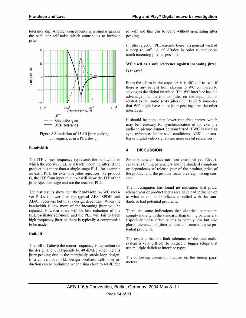
Frandsen and Lave Plug and Play? Digital network investigation
AES 116th Convention, Berlin, Germany, 2004 May 8–11 Page 14 of 31
tolerance dip. Another consequence is a similar gain in the oscillator self-noise which contributes to intrinsic jitter.
Figure 8 Simulation of 13 dB jitter peaking
consequences in a PLL design.
Bandwidth
The JTF corner frequency represents the bandwidth in which the receiver PLL will track incoming jitter. If the product has more than a single stage PLL, for example an extra PLL for extensive jitter rejection like product G, the JTF from input to output will show the JTF of the jitter rejection stage and not the receiver PLL.
The test results show that the bandwidth on WC recei-ver PLLs is lower than the typical AES, SPDIF and ADAT receivers but this is design dependent. When the bandwidth is low more of the incoming jitter will be rejected. However there will be less reduction of the PLL oscillator self-noise and the PLL will fail to track high frequency jitter so there is typically a compromise to be made.
Roll-off
The roll-off above the corner frequency is dependent on the design and will typically be 40 dB/dec when there is jitter peaking due to the marginally stable loop design. In a conventional PLL design oscillator self-noise re-duction can be optimised when using close to 40 dB/dec
roll-off and this can be done without generating jitter peaking.
In jitter rejection PLL-circuits there is a general wish of a steep roll-off e.g. 60 dB/dec in order to reduce as much incoming jitter as possible.
WC used as a safe reference against incoming jitter.
Is it safe?
From the tables in the appendix it is difficult to read if there is any benefit from slaving to WC compared to slaving to the digital interface. The WC interface has the advantage that there is no jitter on the input that is related to the audio (data jitter) but Table 9 indicates that WC might have more jitter peaking than the other interfaces.
It should be noted that lower rate frequencies, which may be necessary for synchronization of for example audio to picture cannot be transferred if WC is used as sync reference. Under such conditions, AES11 or ana-log or digital video signals are more useful references.
4. DISCUSSION
Some parameters have not been examined yet: Electri-cal versus timing parameters and the standard complian-cy dependency of release year of the product, price of the product and the product focus area e.g. mixing con-sole.
The investigation has found no indication that price, release year or product focus area have had influence on to what extent the interfaces complied with the stan-dards or had potential problems.
There are some indications that electrical parameters comply more with the standards than timing parameters. Especially phase offset seems to comply less but also phase tolerance and jitter parameters seem to cause po-tential problems.
The result is that the fault tolerance of the total audio system is very difficult to predict in bigger setups that use multiple deficient interface types.
The following discussion focuses on the timing para-meters.

Frandsen and Lave Plug and Play? Digital network investigation
AES 116th Convention, Berlin, Germany, 2004 May 8–11 Page 15 of 31
4.1. Possible reasons for the observed deficiencies
As mentioned, there are indications that the electrical parameters to a higher degree comply with the stan-dards. A reason could be that the industry has dealt with similar parameters for many years on analog interfaces and is familiar with the importance of them. The electri-cal part of the interfaces might also be less complex to design and test than the timing controlling part.
Timing
One reason for the observed deficiency could be that the industry still might not be fully aware of the complexity of the timing parameters. A possible factor limiting the design verification of the interface could be that it usually takes expensive test equipment to generate and measure phase and jitter.
Regarding standard chips
If the designer uses off-the-shelf components in the design there is often little focus on phase relations. For example, the AES receiver chips on the market often have significant phase offset from the AES stream to the regenerated internal 1Fs signal and similarly on the AES transmitters (an internal square wave signal at 1 times the sample frequency is often referred to as 1Fs). This means that it often takes extra components (e.g. an FPGA) to compensate for the offsets in the standard chips. Another example could be products featuring AES outputs which are made using the on-chip AES transmitters on some DSPs. The AES transmitter on these DSPs may not have any fixed 1Fs relation unless it is made in software by using a timer, which could be started on an internal fixed 1Fs edge. Often those DSPs are targeted for consumer systems which only have digital outputs and therefore don’t need to be synchro-nized. To involve programmers in a standard complian-cy task of this type could result in more complex design flows. A more ideal approach might be to have HW de-signs that assure a fixed 1Fs relation and standard com-pliancy. Reuse of the HW platform this way becomes easy for the system designer.
Deficiency on tolerance to phase offset might be due to similar reasons.
Jitter
Intrinsic jitter, tolerance to jitter and jitter peaking are PLL related parameters. Some designers find PLLs complex and the often used terminology might be far from what is used in conventional HW designs. Not being able to measure the jitter parameters, or not knowing how to do it, might be the most significant reasons for the observed deficiencies.
Specification missing in standards
Most standards do not address phase and jitter issues and there is rarely an inter-format standardisation, with the exception of AES11 and the recently added WC recommendation. Another exception is the TDIF and WC relation, which is specified in the TDIF standard, but rarely met as this investigation shows.
There are historical reasons why phase is not specified in some standards. SPDIF was initially developed for the consumer industry, which until recently has used the interface primarily for chain setups e.g. from a CD player to a receiver-amplifier. Typically this type of setup does not need phase offset and phase tolerance specifications. Because of its small and inexpensive interface front-end, the semi-professional and partly the professional audio industry has adopted the interface with the result that it is now used in setups with increased complexity. The (semi-) professional system complexity very quickly increases to a level where dealing with phase becomes important.
4.2. How to deal with the deficiency
4.2.1. Users
The end-users are most likely helpless with respect to the examined problems because they have few options if a product misbehaves in some situations. Many of the investigated parameters are not easily assessed e.g. through measurements and it is therefore often difficult for the user to locate the exact problem.
However there is a posibility for them. The investiga-tions indicate that locking to the WC interface can opti-mise phase offset and tolerance to phase offset on some products. This has been a rule of thumb in the industry for many years and it is therefore comparable to real life experience. Note that the investigation only indicates

Frandsen and Lave Plug and Play? Digital network investigation
AES 116th Convention, Berlin, Germany, 2004 May 8–11 Page 16 of 31
this phase optimisation meaning that locking to the WC interface does not solve all phase problem situations.
DICE II as IO engine and measurement tool.
Some products provide help for the user to be able to examine the setup without having to buy expensive test equipment. An example is the DICE II chip from TC Applied Technologies [9] which offers extensive on- chip measurement functions including phase offset and sample rate frequency measurements on all inputs. This way the user can get information about the fault tolerance of the total system. Additionally the user will be able to point out potential deficiencies on the pro-ducts connected to the DICE II.
In general the DICE II chip features multiple audio interface types including AES3, ADAT, TDIF, ADC and DAC ports. Additionally high-order jitter rejection and IEEE1394B IEC 61883-6 audio streaming is fea-tured.
4.2.2. Manufacturers
For electrical characteristics the best suggestion might be to increase the effort in complying with the standards available. For the WC interface the designers are guided by the AES11 standard.
Designers should increase their effort in complying with AES11 with regards to phase issues. If AES11 was used for SPDIF, ADAT and TDIF interfaces as well, future networks using point-to-point connections would suffer less from phase related faults. Especially when developing products featuring multiple interface types, the designers should pay attention to AES11 in both the design and the verification phase.
Again with respect to jitter and PLLs, the designers should focus on both the design and the verification phase.
AES3 and AES11 as reference when proposing new
interface types.
It is likely that the number of potential problems increases when the number of different interface types increases in a system. Individual products will continue to support multiple interface types and as more types are developed, the products will start featuring these. Therefore, it will be important to relate the new inter-
face types to the existing ones in order to increase the fault tolerance on the total system.
This can be ensured through standardisation - and perhaps AES11 and its WC recommendation could be used as common standard for future point-to-point stan-dards and - whenever appropriate - for future network standards.
AES3 and AES11 as reference for existing interface
types.
It could improve implementation of existing interface types like ADAT and TDIF if the AES11 phase speci-fications were applied. It would be difficult to apply all the AES3 jitter specifications without compensating for the different bit lengths on the ADAT and TDIF inter-faces. In general it would be beneficial to apply the AES3 jitter peaking specifications to ADAT and TDIF implementations.
4.2.3. The chip industry
It might be possible for the chip manufacturers to further assist the product designer when designing the chips. It would be possible to design chips which made a product design AES11 compliant without the need for adding extra components to compensate for inherent phase offsets in the off-the-shelf chips.
Some deficiencies could be a result of the chip designs not being driven by the professional audio industry. The chips originally being targeted at simpler applications with consumer products and later adopted in profes-sional products (as with the mentioned DSPs including an AES transmitter) mean that not all professional appli-cations have been taken into account.
The development of e.g. the DICE II chip has been dri-ven from the professional audio industry and therefore it is designed to fit complex setups and to provide solid interfaces and tools for the user.
4.3. The next generation of interfaces
This paper has discussed deficiencies observed on point-to-point interfaces known by the professional audio industry. This way of connecting products is not very ideal when setting up a network. Recently inter-faces have been developed which approach the question of connection from a network point of view. But what

Frandsen and Lave Plug and Play? Digital network investigation
AES 116th Convention, Berlin, Germany, 2004 May 8–11 Page 17 of 31
are the demands on a network that would make it close to ideal? Some of the important factors are mentioned here:
• Numerous audio channels
• Several sample rates, high bandwidth
• Zero or minimal audio delay
• No jitter or phase problems
• Easy access to signals
• No re-wiring in order to re-route signals between products
• Easy control and setup e.g. from software
• Good support of known/old interfaces types
IEEE1394 fulfils most of the needs and therefore could a realistic solution.
This calls for interface designs with increased complexi-ty for both the HW and SW part. There is a risk that real life implementations will show numerous proprietary interfaces called “1394” instead of well functioning networks with high system fault margin.
Is the audio industry undermining itself?
So how will the audio industry convince end-users that future networks will work reliably? End-users might have found that known and relatively simple interfaces as for example AES seems to be a problem for manufac-tures to design reliably. A natural assumption for the end-user could then be that manufacturers will find it such a large task to design e.g. IEEE1394 that it might not work well across brands.
In this way the audio industry seems to undermine its perceived reliability by making even simple interfaces deficient.
The consumer industry
Compared to the professional audio industry the consu-mer industry has until recently only focussed a little on some of the network and system parameters. An exam-ple is the SPDIF interface which has primarily been used for chain setups e.g. from a CD player to a recei-ver-amplifier and as a result there has only been one
clock master and one clock slave product at the same time.
It might be a question of time until the consumer indus-try will have to address the issues the professional in-dustry has dealt with for years. Home network with multiple digital sources running simultaneously and multiple listener/viewer locations will dictate the need for addressing the timing parameters investigated in this paper. Such sources and players could be multiple televisions, DVD-players/recorders, set-top boxes, com-puters, hard disks and telephones which could be lo-cated at different places.
5. CONCLUSIONS
In conclusion, we have demonstrated that digital interfa-ces like AES, SPDIF, ADAT, TDIF and WC in real life implementations have potential problems which are not all addressed by the standards for the individual inter-face types. Connecting equipment in an ideal way may be impossible even for an experienced engineer, so sys-tem reliability can end up being different each time a machine is turned on or synchronized.
We have learned that primarily timing as opposed to electrical parameters are subject to deficiency. The number of potential problems seems independent of the price of the product, of the product release year and of the product focus area e.g. a mixing console.
There are indications that the number of interface types on a product results in a higher probability of problems on the product. The problems do not solely belong to one interface type; there are problems to be found on implementations of every one of the tested interface types.
Insufficient specification in standards, insufficient knowledge of the interface parameters and insufficient verification during the design phase might be reasons for the interface deficiencies presented in this paper.
A suggestion could be to relate new interface proposals to existing interfaces. In this way deficiency in complex network setups using multiple interface types (new and old) might be reduced and system fault tolerance increa-sed. Perhaps AES11 and its WC recommendation could be used as common standard for future point-to-point standards and - whenever appropriate - for future net-work standards.

Frandsen and Lave Plug and Play? Digital network investigation
AES 116th Convention, Berlin, Germany, 2004 May 8–11 Page 18 of 31
The consumer audio industry has paid little attention to complex networks until now but this may have to change in near future. Home networks with multiple digital sources running simultaneously and multiple listener/viewer locations will dictate the need for addressing the parameters investigated in this paper.
End-users are dependent on the audio industry to design well functioning interfaces because they are unable to address potential deficiencies. If the audio industry does not design well working conventional digital interfaces there is a risk that the users will not trust and accept new and highly complex networks like IEEE1394. In this way the industry might undermine itself by designing deficient conventional digital interfaces.
6. REFERENCES
[1] AES3-1992 (r1997) incl. amendment 1-4, AES recommended practice for digital audio engineering – Serial transmission format for two-channel linear-ly represented digital audio data.
[2] IEC60958-3, Digital audio interface – Consumer applications.
[3] AES11-2003, AES recommended practice for digi-tal audio engineering – Synchronization of digital audio equipment in studio operations.
[4] Audio Precision, Tech note 26, The AES3 and IEC60958 Digital Interface, by Julian Dunn. Associated AP measurement files. Available at www.ap.com.
[5] AES-2id-1996 (reaffirmed 2001), AES information document for digital audio engineering – Guideli-nes for use of the AES3 interface.
[6] Operation manuals for all the products used in the test. They were all available on the internet at the manufacturers’ websites.
[7] Alesis Corp., ADAT specifications. NDA applies.
[8] TEAC Corp., TDIF-1 specifications. NDA applies.
[9] TC Applied Technologies www.tctechnologies.tc. Information regarding the DICE II chip, which features multiple audio interface types: AES3, ADAT, TDIF, ADC and DAC ports. Additionally
high-order jitter rejection and IEEE1394B IEC 61883-6 audio streaming is featured.

Frandsen and Lave Plug and Play? Digital network investigation
AES 116th Convention, Berlin, Germany, 2004 May 8–11 Page 19 of 31
7. APPENDIX Product focus area DUT Approx. price USD Release year Interfaces
AES SPDIF ADAT
A 12500 1997
TDIF SPDIF B 4400 1998 ADAT AES
SPDIF ADAT TDIF
C 9700 1996
WC SPDIF ADAT TDIF
Mixing console
D 2000 2001
WC AES
SPDIF ADAT
E 3900 1996
WC AES F 18000 2000 WC AES G 10000 1999 WC AES
SPDIF H 3300 1999
WC AES
SPDIF I 4400 1999
WC J 900 1999 SPDIF
AES
Effects processing
K 8000 2000 WC
ADAT L 330 2003 WC
ADAT M 1900 1999 WC
ADAT TDIF
ADC/DAC
N 2300 2001
WC AES
ADAT TDIF
O 1900 2001
WC AES
ADAT
Format conversion
P 630 2001
WC AES
SPDIF ADAT
Q 1200 1998
WC SPDIF ADAT
Computer interfaces
R 410 1999
WC S 2200 1999 ADAT T 2400 1996 ADAT
ADAT
HD recorder
U 4200 2001 WC AES Speakers V 2600 2001 WC
Table 10 Overview of product focus area, DUT name, price, release year and featured interfaces.

Frandsen and Lave Plug and Play? Digital network investigation
AES 116th Convention, Berlin, Germany, 2004 May 8–11 Page 20 of 31
Internal sample rate deviation Intrinsic jitter 44.1/88.2 kHz 48/96 kHz 700 Hz HPF 50 Hz HPF
DUT
ppm ns peak A 0 0 1.9 2.2 B 0 2.2 2.5 C 0 0 1.8 2 D -13 33 0.7 0.9 E -11 -11 1.2 2 F -7 -3 0.5 0.7 G -26 -34 0.7 0.9 H 13 3 1.5 1.7 I -4.5 -5 12 13 J -5 -18 1 1.2 K -4 -3 0.9 1.2 L 76 65 2.4 2.6 M 23 23 2.2 2.4 N -7 24 2.6 2.9 O -3 -2 1.3 1.7 Q -12 -9 0.8 1 R 11 7 0.6 1 S -8 -22 2.5 2.7 T 47 48 2 2.2 U -49 35 2.5 2.6
Mean value 1.3 6.8 2.1 2.4 +/- 1, grade 1 +/- 1, grade 1 4.1 AES standard +/- 10, grade 2 +/- 10, grade 2 +/- 50, level 1 +/- 50, level 1 8.1 60958 standard
+/-1000, level 2 +/-1000, level 2
Table 11 Internal sample rate deviation and intrinsic jitter when clock master. Note: Intrinsic jitter measurements on product L, M, N, S, T, U are affected by the RME ADAT/AES converter.
The result tables in this paper shows two different shades. A light grey for parameters that might be potential problems in a digital setup but are not incompliant with any standard. A dark grey for parameters that are incom-pliant with a standard.
The abbreviations used in the results tables are explained here:
UtL: The product was unable to lock to the signal.
Hi Z: Using e.g. 75 Ω source impedance did not affect the input level to the product so the input impedance was regarded as “high”.
Incs: The phase offset or data reading point is inconsistent from lock-up to lock-up.

Frandsen and Lave Plug and Play? Digital network investigation
AES 116th Convention, Berlin, Germany, 2004 May 8–11 Page 21 of 31
13 Hys: There is 13% frame period hysteresis around receiver data reading point. The data reading point will move depending on incoming phase to optimise location of the hysteresis. Consequently the resulting phase tolerance will be bigger than 13% of a sample period.
2/-3 Win: There is a +2%/-3% frame period window in which the data will be received correctly. Outside this window the receiver will not accept data.
NDt: The data reading point was not detectable while moving the phase from +50% to -50% of a sample period and/or applying 25 UI peak-peak jitter (100 Hz sine wave type).
0.5/-0.5 Win Incs: Like “Win” but the location of the window is inconsistent from lock-up to lock-up.
Output characteristics Impedance Output level
Input level tolerance
Rise time HPF corner Ringing Input Output
DUT
Vpp mVpp ns kHz Vpp Ω A 1.9 1100 75 15 0 96 56 C 4.8 280 28 20 0 110 42 E 4.75 200 33 15 0 106 90 F 4.8 100 30 15 0 112 98 G 4.3 90 40 15 0 110 115 H 4.3 130 60 10 0 110 115 I 4.6 100 28 10 0 108 103 K 5.9 180 30 25 0.2 104 12 O 5 170 33 55 0 110 127 P 3.8 130 30 5 0 116 138 Q 4.8 250 33 160 0 90 110 V 440 104 Mean value 4.4 264 38 31 106 91 AES standard 2-7 <200 5-30 <100 88-132 88-132
Table 12 AES electrical characteristics

Frandsen and Lave Plug and Play? Digital network investigation
AES 116th Convention, Berlin, Germany, 2004 May 8–11 Page 22 of 31
Phase offset
Phase offset across interfaces. Below are outputs
When slave AES SPDIF ADAT TDIF WC
DUT
% 1/Fs % 1/Fs A 0 0 35 -40 C 0.7 -32 0.7 -49.3 25.5 0.5 E 12.2 0.3 F Incs 17 G 0.3 0.6 H Incs Incs I Incs -9 K -31 20 O Incs 6.2 25 24 P 11 -0.5 50.3 Q Incs Incs Incs Incs V AES standard +/-5 +/-5
Table 13 AES phase offset from in-to-out and across interfaces.
Phase tolerance
Phase tolerance across interfaces. Below are references
When master Input 1 WC SPDIF ADAT TDIF
DUT
% 1/Fs % 1/Fs A NDt C NDt NDt NDt NDt 40 Hys NDt E -19.5 -20 F 25 Incs 43 G 26 -6 26 H -55 I 17 K 25 25 O -7 -28 -28 -2.4 -32 P 16 Hys Q 25 Incs V 26 27 AES standard +/-25 +/-25
Table 14 AES phase tolerance when clock master and clock slave to other interfaces. The column “Input 1” means that AES input 1 is reference and the tolerance on AES input 2 is tested on a product with multiple AES inputs.

Frandsen and Lave Plug and Play? Digital network investigation
AES 116th Convention, Berlin, Germany, 2004 May 8–11 Page 23 of 31
Intrinsic jitter slave Jitter tolerance Jitter transfer function,
JTF 700 Hz HPF 50 Hz HPF wide 100 Hz 1 kHz 10 kHz Peaking BW Roll-off
DUT
ns peak UI peak dB Hz dB/dec A 0.18 12.75 12.75 0.5 C 8 15 0.23 12.75 3.5 1.5 0 4000 10 E 1.8 2.7 0.11 9.7 9.7 0.7 0 500 20 F 0.5 1 0.19 12.75 12.75 1 0 200 40 G 0.7 0.9 0.2 10 10 2 0 10 40 H 1.6 2 0.2 10 3 2.4 0.5 70000 40 I 12 13 0.21 12.75 12.75 2.1 10 7000 40 K 0.9 1.9 0.18 8 6.6 1 13 250 40 O 2.1 2.7 0.22 12.75 4.5 0.5 0 18000 20 P 5.2 6.8 0.21 12.75 1.4 0.37 1 4000 20 Q 2.9 3.5 0.16 12.75 12.75 0.57 1 20000 20 V 0.28 12.75 3.4 4 Mean value 3.6 5.0 0.20 11.6 7.8 1.4 AES standard 4.1 0.125 5 1 0.125 <2
Table 15 AES intrinsic jitter when slave, jitter tolerance and jitter transfer function.
Output level
Input level tolerance
Output characteristics Impedance
Rise time HPF corner Ringing Input Output
DUT
Vpp mVpp
ns kHz Vpp Ω A 0.97 450 100 5 0 85 75 B 0.53 220 33 50 0 77 81 C 0.49 280 33 20 0 75 72 D 0.49 30 30 10 0 75 73 E 0.9 90 60 5 0 78 69 H 0.54 110 30 10 0 81 77 I 0.91 110 40 5 0 78 75 J 0.5 110 30 5 0 80 78 Q 0.45 100 35 100 0 55 60 R 1 180 60 30 0 90 50 Mean value 0.68 168 45 24 0 77.4 71 60958 standard 0.4 - 0.6 <200 <65 <100 71-79 71-79
Table 16 SPDIF electrical characteristics.

Frandsen and Lave Plug and Play? Digital network investigation
AES 116th Convention, Berlin, Germany, 2004 May 8–11 Page 24 of 31
Phase offset
Phase offset across interfaces. Below are outputs
When slave AES ADAT TDIF WC
DUT
% 1/Fs % 1/Fs A B 0.5 -4 C 0.7 0.7 -49 26 0.5 D -14 18 -17 E 12.2 12.2 H Incs Incs I Incs -9 J 5.8 Q Incs Incs Incs Incs R Incs Incs Incs 60958 standard AES standard +/-5 +/-5
Table 17 SPDIF phase offset from in-to-out and across interfaces.
Phase tolerance
Phase tolerance across interfaces. Below are references
When master Input 1 WC AES ADAT TDIF
DUT
% 1/Fs % 1/Fs A NDt B NDt NDt C NDt NDt NDt 40 Hys NDt D E -19.5 -20 H -55 I 17 J -9.5 Q 25 Incs R 60958 standard AES standard +/-25 +/-25
Table 18 SPDIF phase tolerance when clock master and clock slave to other interfaces. The column “Input 1” means that SPDIF input 1 is reference and the tolerance on SPDIF input 2 is tested on a product with multiple SPDIF
inputs.

Frandsen and Lave Plug and Play? Digital network investigation
AES 116th Convention, Berlin, Germany, 2004 May 8–11 Page 25 of 31
Intrinsic jitter slave Jitter tolerance Jitter transfer function, JTF
700 Hz HPF 50 Hz HPF wide 100 Hz 1 kHz 10 kHz Peaking BW Roll-off
DUT
ns peak UI peak dB Hz dB/dec A 0.18 12.75 12.75 0.5 B 4.7 4.9 0.06 12.75 1 0.1 7 7000 40 C 8 13 0.22 12.75 3.4 1.6 0 4000 10 D 0.27 7 0.3 3 E 1.8 2.7 0.11 9.7 9.7 0.7 0 500 20 H 2.5 2.8 0.2 10 3 2.4 0.5 70000 40 I 8 10 0.21 12.75 12.75 2 8 6000 40 J 1.2 1.4 0.18 12.75 12.75 1.1 1.5 30000 20 Q 3.4 3.5 0.17 12.75 12.75 0.64 1 20000 10 R 7 15 3 400 40 Mean value 4.6 6.7 0.18 11.5 7.6 1.3 60958 standard 8.1 0.1 0.25 0.125 0.125 <3
Table 19 SPDIF intrinsic jitter when slave, jitter tolerance and jitter transfer function.
Phase offset
Phase offset across interfaces. Below are outputs
When slave AES SPDIF TDIF WC
DUT
% 1/Fs % 1/Fs A B 1.2 4.8 C 1 -49 -49 -25 -49 D Incs Incs Incs Incs E 1.9 -3.6 L Incs 50.4 M 1.1 50.4 N 7.6 -42 32.6 O Incs 7.2 31 31 P 49.2 Incs 0.2 Q Incs Incs Incs Incs R 1 3 1 S Incs T 5.7 U AES standard +/-5 +/-5
Table 20 ADAT phase offset from in-to-out and across interfaces.

Frandsen and Lave Plug and Play? Digital network investigation
AES 116th Convention, Berlin, Germany, 2004 May 8–11 Page 26 of 31
Phase
tolerance Phase tolerance across interfaces.
Below are references When master input 1 WC AES SPDIF TDIF
DUT
% 1/Fs % 1/Fs A NDt B 43 Hys 43 Hys C -23 28 26 26 3.8 D 7.2 Incs 9.6 E -10 -15 L 6.2 -41 M 2.4/-3.1 Win 4/-1.5 Win 53/-48 Win N 19 Hys 19 Hys O -5 -28 -12 -36 P 5/-5 Win Q -22 Incs Incs Incs R S -2.4 T U 6 8 AES standard +/-25
Table 21 ADAT phase tolerance when clock master and clock slave to other interfaces. The column “Input 1” means that ADAT input 1 is reference and the tolerance on ADAT input 2 is tested on a product with multiple ADAT
inputs.

Frandsen and Lave Plug and Play? Digital network investigation
AES 116th Convention, Berlin, Germany, 2004 May 8–11 Page 27 of 31
Intrinsic jitter slave Jitter tolerance Jitter transfer function, JTF
700 Hz HPF 50 Hz HPF wide 100 Hz 1 kHz 10 kHz Peaking BW Roll-off
DUT
ns peak UI peak dB Hz dB/dec A 0.16 12.75 2.5 0.4 B 12 13 0.04 12.75 0.9 0.05 12 C 8 10 0.14 10 2 0.22 0.5 3000 10 D 2.7 3.6 0.2 12.75 2.1 0.5 2 3000 20 E 3 7 0.15 11 5 0.4 0 300 20 L 2.2 2.6 0.04 12.75 0.4 0.15 2 4000 20 M 3 3.2 0.1 0.6 0.17 0.14 0 500 20 N 6.5 6.5 0.12 12.75 1.2 0.12 0 30000 20 O 2.3 2.4 0.16 12.75 1.2 0.25 0 50000 20 P 0.2 12.75 1.1 0.5 2 4000 20 Q 11 12 0.07 12.75 1.2 0.11 0 15000 20 R 3.6 3.8 0 30000 20 S 7.5 8.5 0.04 12.75 2.6 0.14 5 45000 40 T 8 10 0.06 12.75 1 0.12 0 30000 20 U 0.13 12.75 5.5 0.35 Mean value 0.12 11.56 1.9 0.25 AES standard 4.1 0.125 5 1 0.125 <2
Table 22 ADAT intrinsic jitter when slave, jitter tolerance and jitter transfer function. Note: All intrinsic jitter measurements are affected by the RME ADAT/AES converter; therefore no mean value has been calculated.
Output level Input level tolerance
Output characteristics
Impedance
Rise time Ringing Input Output
DUT
Vpp mVpp ns Vpp Ω
A 2.1 5 0.7 Hi Z 75 C 2.1 3400 25 0 80 75 D 1.6 40 0.3 Hi Z 97 N 1.7 1500 5 0.5 Hi Z 75 O 2.1 1300 5 0.5 Hi Z 64 Mean value 1.9 2070 16 0.4 77 TDIF standard 2-3 >1k5 45-67
Table 23 TDIF electrical characteristics.

Frandsen and Lave Plug and Play? Digital network investigation
AES 116th Convention, Berlin, Germany, 2004 May 8–11 Page 28 of 31
Phase offset
Phase offset across interfaces. Below are outputs
When slave AES SPDIF ADAT WC
DUT
% 1/Fs % 1/Fs A C 0.6 -25 -25 26 26 D N 0.1 -24 0 O 0 -25 19 0 TDIF standard +/-0.24 +/-0.24 AES standard -/- 5
Table 24 TDIF phase offset from in-to-out and across interfaces.
Phase tolerance
Phase tolerance across interfaces. Below are references
When master Input 1 WC AES SPDIF ADAT
DUT
% 1/Fs % 1/Fs A 8.2 C 47 Hys 47 Hys 47 Hys 47 Hys 47 Hys D 0.5/-0.5 Win 0.5/-0.5 Win 0.5/-0.5 Win Incs N 19 Hys 19 Hys O -6 -3 -28 25 TDIF standard AES standard +/-25
Table 25 TDIF phase tolerance when clock master and clock slave to other interfaces. The column “Input 1” means that TDIF input 1 is reference and the tolerance on TDIF input 2 is tested on a product with multiple TDIF inputs.

Frandsen and Lave Plug and Play? Digital network investigation
AES 116th Convention, Berlin, Germany, 2004 May 8–11 Page 29 of 31
Intrinsic jitter slave Jitter tolerance Jitter transfer function, JTF
700 Hz HPF 50 Hz HPF wide 100 Hz 1 kHz 10 kHz Peaking BW Roll-off
DUT
ns peak UI peak dB Hz dB/dec A 0.21 8 5 0.5 C 8 13 0.22 10 1 0.45 0 2500 10 D 0.15 0.7 0.7 0.7 N 3.1 3.8 0.24 8 0.8 0.1 1 4000 20 O 3 3.5 0.22 12.75 3 0.5 0 4000 40 Mean value 0.21 7.9 2.1 2.25 TDIF standard AES standard 4.1 0.125 5 1 0.125 <2
Table 26 TDIF intrinsic jitter when slave, jitter tolerance and jitter transfer function. Note: All intrinsic jitter measurements are affected by the RME TDIF/AES converter; therefore no mean value has been calculated.
Output level Input level tolerance
Output characteristics
Impedance
Rise time Ringing Input Output
DUT
Vpp mVpp
ns Vpp Ω C 3.1 1600 25 0 75 10 D 3.2 1700 50 0.2 Hi Z 56 E 100 86 F 3.3 1800 10 3 50 21 G 50 81 H 3.1 2000 4 0.3 80 51 I 0.15 2400 100 0 80 2400 K 3 1600 100 0.3 88 25 L 1000 Hi Z M 3 410 4 0.3 75 70 N 4 500 5 0 Hi Z 19 O 4 110 3 0.3 Hi Z 165 P 4.6 1800 250 0 81 16 Q 3.3 15 0.3 30 R 4 1500 4 0.3 105 22 U 3.7 1900 5 0.2 86 30 V 50 Hi Z Mean value 3.3 1150 44 0.4 225 AES11-2003 <0.4/>2.4 V <0.4/>2.4 V
Table 27 WC electrical characteristics.

Frandsen and Lave Plug and Play? Digital network investigation
AES 116th Convention, Berlin, Germany, 2004 May 8–11 Page 30 of 31
Phase offset Phase offset across interfaces. Below are outputs
When slave AES SPDIF ADAT TDIF
DUT
% 1/Fs % 1/Fs C 0.7 0.7 0.7 -49 26 D 0.7 17 2.9 25.7 E F 0.2 Incs G H 1.2 2.5 I 2.4 Incs K 1.7 4.2 L M 0.2 50.7 N 0.2 -24.9 0 O 0.2 -25 -31 0 P 0.1 14 49.2 Q R 2 4 2 U 1 1.4 V AES11-2003 +/-5 +/-5
Table 28 WC phase offset from in-to-out and across interfaces.

Frandsen and Lave Plug and Play? Digital network investigation
AES 116th Convention, Berlin, Germany, 2004 May 8–11 Page 31 of 31
Intrinsic jitter slave Jitter tolerance Jitter transfer function, JTF
700 Hz HPF 50 Hz HPF 100 Hz Peaking BW Roll-off
DUT
ns peak UI peak dB Hz dB/dec C 9 17 12.75 0.5 3000 10 D 2.8 3 12.75 8 7000 40 E 1.8 2.7 9.7 0 500 20 F 0.5 1 5 0 200 40 G 0.7 0.9 10 0 10 40 H 3 7 9 0 450 20 I 8 9 12.75 8 6000 40 K 0.9 1.6 7.5 13 250 40 L 3.3 3.6 12.75 1 2000 40 M 2.2 2.4 0 500 20 N 10 15 7 1 2000 20 O 2.6 2.7 12.75 0 4000 40 P 3.6 4 12.75 17 4000 40 Q R 6 12 3 400 40 U 2.5 3 12.75 4 2500 40 V 12.75 Mean value 3.8 5.7 10.7 AES standard 4.1 5 <2
Table 29 WC intrinsic jitter when slave, jitter tolerance and jitter transfer function. Note: Intrinsic jitter measurements L, M, N and U are affected by the RME ADAT/TDIF/AES converter.