author's personal copy - uth circuits and systems group · [email protected] nikolaos...
TRANSCRIPT

1 23
Circuits, Systems, and SignalProcessing ISSN 0278-081X Circuits Syst Signal ProcessDOI 10.1007/s00034-015-0082-9
Phase Interpolator with Improved Linearity
George Souliotis, Costas Laoudias, FotisPlessas & Nikolaos Terzopoulos

1 23
Your article is protected by copyright and all
rights are held exclusively by Springer Science
+Business Media New York. This e-offprint is
for personal use only and shall not be self-
archived in electronic repositories. If you wish
to self-archive your article, please use the
accepted manuscript version for posting on
your own website. You may further deposit
the accepted manuscript version in any
repository, provided it is only made publicly
available 12 months after official publication
or later and provided acknowledgement is
given to the original source of publication
and a link is inserted to the published article
on Springer's website. The link must be
accompanied by the following text: "The final
publication is available at link.springer.com”.

Circuits Syst Signal ProcessDOI 10.1007/s00034-015-0082-9
Phase Interpolator with Improved Linearity
George Souliotis1 · Costas Laoudias1 ·Fotis Plessas2 · Nikolaos Terzopoulos3
Received: 12 January 2014 / Revised: 16 May 2015 / Accepted: 18 May 2015© Springer Science+Business Media New York 2015
Abstract An analog phase interpolator with improved step linearity is presented inthis paper. The linearity is improved by setting the time constant of the output nodesin suitable value and by employing a fine trimming technique. The performance andthe improved linearity have been verified with post-layout simulations using a well-established CMOS 65nm technology and transistors with standard threshold voltages.The clock frequency is at 2.5GHz and the core voltage supply at 1.2V. Its low phasenoise makes the circuit suitable for high-speed systems where low jitter performanceis required.
Keywords Phase interpolator · Clock and data recovery · SerDes
B George [email protected]
Costas [email protected]
Fotis [email protected]
Nikolaos [email protected]
1 Department of Physics, University of Patras, Patras, Greece
2 Department of Electrical and Computer Engineering, University of Thessaly, Volos, Greece
3 Department of Computing and Communication Technologies, Faculty of Technology, Design andEnvironment, Oxford Brookes University, Wheatley, Oxford, UK
Author's personal copy

Circuits Syst Signal Process
1 Introduction
The phase interpolator (PI) is a critical block in the clock and data recovery (CDR)loop. PI is interposed in SerDes systems, between the PLL and the data samplers, inorder to shift the clock phase accordingly in the data sampling window. It receives twoclocks of the same frequency with phases φ andψ , respectively, and generates a clockoutput whose phase Θ is the weighted summation of the two input phases [11]. Theideal PI must generate a number of equally spaced phase steps for a full cycle from 0◦to 360◦. In fact, the generation of equally spaced steps is a hard process in real PIs, andthis is one of the major problems that needs correction for a proper operation. Severaldigital or analog PI circuits have been proposed in the literature focusingmostly in steplinearity [3] with a robust circuit and design flexibility. Some papers propose simplemethods to improve linearity, like better control, or feedback from the output, whilesome others propose more complicated techniques, like multiple step stages [2,7,12],but some of them are not suitable for high-speed systems [8]. The specifications forthe phase linearity and step size depend on the system architecture, where usually, anumber of 32 steps in total is good enough for a typical high-speed de-serializer. Thephase step should not be too short to follow the long phase variations within specificclock cycles, but also should not be too long because it may create longer phase stepsthan the required ones, and then, the clock could be out of the valid data window. Acontroller is used to drive the steps of the phase interpolator, up or down. This is a fullydigital circuit operating as an up/down counter. Also, in most of the high-frequencysystems and especially when a spread spectrum clock is used, the phase changes musttake place very fast, ideally, in only one bit period in order that the clock will remainin the valid window of the CDR; therefore, both the phase interpolation and its digitalcontroller must be high-speed circuits.
Two generic methods are followed in designing PIs: the analog and the digital.Usually, the analog PIs are employed in high-speed systems with high operating fre-quency. Some systems use low-frequency PI, but they require a really large number ofinput phases to feed its input [3]. The large number of phases and the multiple clockdistribution make the layout a tough procedure, especially when used in high bit-ratesystems. Also, for the digital PIs, highly accurate phases must be generated and dis-tributed from the oscillator. A digital PI proposed in [10] is very simple in designand shows improved linearity but offers small number of steps with large delays, andtherefore, it is not suitable for high-speed architectures.
The analog PI is based on the weighted current summation of the two input clocks.The topology is constructed from two arrays of controlled current-mode logic (CML)buffers, as shown in Fig. 1 [1–3,6,9,11,13]. Usually, two clocks with 90◦ phase dif-ference feed the input. By selecting the combinations of 0 and 90 phases and theirinversions through multiplexers, all the possible phases for a circle of 360 are avail-able, as shown in Fig. 2. The output of the PI is the corrected in phase clock whichis a CML signal. Therefore, a CML-to-CMOS converter is required to feed forwardall the digital cells. Also, a digital controller controls the operation of the interpolatorincreasing or decreasing the phase, one step each time.
A flexible, analog-based PI with improved step linearity is proposed in this paper.The improvement is achieved by introducing two techniques; firstly, an integral of the
Author's personal copy

Circuits Syst Signal Process
Fig. 1 The analog PI
output signal is produced, and secondly, a fine trimming is carried out by increasingthe resolution. The paper is organized as follows: In Sect. 2, the design of the proposedPI is described and the nonlinearity effects are explained. In Sect. 3, the theoreticalanalysis and some linearity improvements are provided, and in Sect. 3, the simulationresults are presented before and after the linearity improvement. Finally, the resultsregarding the PI performance are summarized.
Author's personal copy

Circuits Syst Signal Process
Fig. 2 The topology of the PI
2 The Phase Interpolator
PI receives two clock phases and generates intermediate phases with specific steps.Usually, the input signals, in analog PIs, are of CML type and have a phase differenceof 90◦ in order to produce intermediate phase shifts from 0◦ to 90◦. The full range from0◦ to 360◦ is produced by inverting the inputs, as shown in Fig. 2, giving four quartersof 90◦ each. The output is also of a CML type and is produced by the weighted currentsummation of two currents, based on the topology shown in Fig. 1. Two groups ofdifferential pairs are connected on the same output, terminated by resistors RL . Eachgroup is an array of the same differential pairs with switches connected on theiroutputs. The differential pair is the PI unit cell and is controlled by Ictl control signalthat enables or disables the output current resulting to the total weighted current. InFig. 1, the total capacitance CL connected at the output is depicted by dashed lines.This is the total capacitance including all the parasitic effects and has a significantcontribution to phase interpolator operation.
The digitally controlled weighted output current is given by,
Iout(t) = nIout1 + (N − n)Iout2, n = N : 0 (1)
where the two currents Iout1 and Iout2 have phase difference 90◦. N and n are integers,and the intermediate phases generated by the phase interpolator is N + 1 resulting toN phase steps. In (1), both currents have the same amplitude Ip.
The weight of currents Iout1 and Iout2 is controlled by enabling or disabling thecorresponding number of PI unit cells, through the ports Ictl depicted in Fig. 1. A PIcontroller produces the corresponding signals every time an up/down step is required.Its most simplified version is a thermometer coder which enables or disables only oneunit cell each time to increase or decrease the phase step.
Author's personal copy

Circuits Syst Signal Process
Fig. 3 PI a input, b ideal output, c real output and d improved output
Amore careful view on (1) shows some potential problems. Assuming that the idealinput signals are shown in Fig. 3a, where the phase 0◦ signal is depicted in black andthe 90◦ in red color, then according to (1), the resulted ideal current is a stepwise signalconsisting of the weighted contribution of each input, as shown in Fig. 3b. The outputvoltage also takes a similar form according to the relation Vout = Iout · RL . In Fig. 3b,a case of eight phases is shown, with the phase number 0 to correspond to phase 0◦ andthe phase number 7, depicted in red color, to phase 90◦. For a better understanding,the phase number 1 is depicted in green color. The stepwise output in its ideal formis not viable in the analog or digital domain, because these steps cannot be processedby a typical following stage, in example a buffer, which requires a normal rising orfalling edge to distinguish the low from high state. However, in practice, the idealoutput is not expected to be shown in a real high-speed circuit, because of the parasiticcapacitances of the output nodes. Instead, an integral of this signal is produced, asshown in Fig. 3c. In that case, the parasitic capacitances act beneficially at the outputnodes, creating the output in Fig. 3c, which can be exploited to create phase delays,clearly separated from each other. For example, the phase step 1, indicated with thegreen line, is now clearly separated from the previous and the next step.
Author's personal copy

Circuits Syst Signal Process
Fig. 4 Equivalent circuit of PI output
The inherent problem at PI’s output is that although the final phase steps are avail-able, each step has a different shape, different rise and fall time and does not follow theprevious with a uniform way. Therefore, each step does not produce the equal delay.
A simplified analysis for the nonlinearity is provided in [13] which predicts an erroron the phase step, due to the exponential form of the output. In [3,4,7], it is reportedthat the interpolator cells should be asymmetrically weighted, 40% for leading phaseand 60% for lagging phase, in order to place the interpolated clock phase in the middleof two adjacent clock phases. However, this asymmetric structure is sensitive to devicemismatch, and this increases the risk of amisalignment of the interpolated phase. Thus,interpolator cells with symmetrical structure were finally preferred in [7] to eliminatethat risk.
3 Theoretical Analysis and Improvements
The output topology of the PI in Fig. 1 can be represented by the equivalent circuitshown in Fig. 4. For simplicity and without losing the concept, only one of the differ-ential outputs is shown. Vout is the output voltage corresponding to the output nodesOut, Iout1 and Iout2 are the output currents generated by the output transistors, RL is theterminating resistor, ro is the total equivalent output resistance of the transistors in theinterpolator unit cells, and CL is the total capacitance at the output nodes, includingall the parasitic capacitances and any other capacitive load charging the output nodes.After a routine analysis, it can be found that the differential equation of the circuit canbe given as,
RLCLdVoutdt
= VDD −(RL
ro+ 1
)Vout − RL (Iout1 + Iout2) (2)
As RL << ro, it isRLro
+ 1 ∼= 1. Then, this first-order linear constant-coefficientordinary differential equation (LCCODE) can be given as,
RLCLdVoutdt
+ Vout = VDD − RL (Iout1 + Iout2) (3)
The homogeneous solution can be found by setting the right side to zero. The solutionin (3) is given by setting,
Author's personal copy

Circuits Syst Signal Process
Vout (t) = Ae−t/τ (4)
where A is a constant and τ = RLCL is the time constant. To resolve for the totalresponse, the undetermined coefficient can be a function of time as,
Vout(t) = A (t) e−t/τ (5)
Substituting (5) into the differential Eq. (3) results in
τ
[A′(t)e−t/τ − 1
τA(t)e−t/τ
]+ A(t)e−t/τ = VDD − RL(Iout1 + Iout2) (6)
From (6), it can be easily found that
A(t) = 1
τ
∫ t
x=0
[ex/τ (VDD − RL (Iout)) dx
] + VDD (7)
The last term VDD in (6) is an initial condition assuming that the capacitor CL ischarged on that voltage for t = 0, according to Fig. 4.
Finally, substituting (7) into (5) results in the solution of the differential equation,
Vout (t) = 1
τe−t/τ ·
∫ t
x=0
[ex/τ (VDD − RL (Iout)) dx
] + VDDe−t/τ (8)
Also, Iout is the summation of the drain currents of the output transistors shown inFig. 1.
Iout = Iout1 + Iout2 (9)
The output currents in their ideal form can be described from weighted pulses. If N isthe total number of phases from 0 phase to 90◦ phase and n is the specific phase, thenIout1 and Iout2 can be given by the following expressions,
Iout1 = ((N−1)−n)N−1 I p
[u (t − 0) − u
(t − T
2
)], n = 0, 1, 2, . . . N − 1
Iout2 = nN−1 I p
[u
(t − T
4
) − u(t − 3T
4
)], n = 0, 1, 2, . . . N − 1
}(10)
where Ip is the amplitude of currents Iout1 and Iouts2, according to (1).In frequency domain, the transfer function corresponds to a first-order lowpass
filter,
H(s) = 1
τ s + 1(11)
where τ is the time constant. If τ takes a low value, for example 0.2, then the outputis of the form as shown in Fig. 3c, which is similar to the expected real circuit.
A way for improving the shape of the output signal is to make the edges evensmoother by taking the integral of that output. This can improve the linearity of riseand fall edges, resulting in an improved step linearity. Enlarging the time constant τ ,for example by five times, then the output takes the form of Fig. 3d, which shows animproved shape with less edges comparing with that of Fig. 3c. The change of the time
Author's personal copy

Circuits Syst Signal Process
constant τ is easily realized, in a real circuit, by simply adding an extra capacitor onthe output nodes. The drawback here is that, although a high capacitor improves thelinearity, the output swing is reduced significantly, because the output node operatesobeying the lowpass transfer function, as defined in (11). Therefore, there is a trade-off between the time constant and voltage swing. The exact value of the additionalcapacitor is not critical; however, a suitable value can be found by the time constantτ defined at the output node. If τo corresponds to the operating frequency ωo of thephase interpolator, then τo = 1/ωo and the suitable value for the total capacitance CL
is found by setting τ = 2τo, which is a good compromise between linearity and outputswing,
CL = 2
RLωo(12)
In (12), CL is the total value, including the additional capacitor and the parasiticcapacitive load. Therefore, the final calculation of the additional capacitor can befound by taking into account the parasitic elements which can be found accuratelyafter the layout extraction. Nevertheless, the additional capacitor is the dominant termin this procedure.
However, even after that method, the linearity is still not greatly improved. A rel-atively easy procedure to improve the linearity even more is to create a higher stepresolution and to keep the best eight steps among them for phases from 0◦ to 90◦.Designing a PI with the number of steps multiplied by 4 (32 steps) for 0◦ to 90◦, byequally divided currents which produce again nonlinear steps, is a relatively straightforward procedure. The selection of the 8 steps among the 32 steps, not necessarilyin equally increasing sequence, can give steps with approximated linear relation. Thefinal 8 steps are selected with an order suitable to produce equally shifted steps.
The exact, increased resolution is decided by the step error requirement. Eachunit cell shown in Fig. 1 splits k times into sub-unit cells. In this design, k was setequal to 4 to comply with the step error specifications, resulting to 32 steps in totalfor 0 to 90◦. All the transistors of the sub-unit cell have k times smaller width thanthe corresponding transistors of the unit cell and also are biased by k times smallercurrent. So, after the split, there are employed totally (k × N ) sub-unit cells meaningthat the controller must control (k × N ) devices. Except this controller overhead, thetotal design is same in terms of layout dimensions and power consumption, becausethere are k times more cells which, however, are k times smaller in layout and currentdissipation. The important point is that the phase interpolator finally dissipates thesame current after the cells splitting, keeping the same performance. The controller,however, must bemodified because as explained previously, it is programmed to selectgroups of sub-unit cells resulting to the best Nsteps among the totally available k× Nsteps in the high-resolution topology. Each group contains different number of sub-unit cells depending on the compensation which is required. If no compensation isrequired for a specific step, then the group contains k sub-unit cells otherwise containsless or greater number than k. Finally, the new controller is again a thermometer coder,but modified in order to enable/disable more than one sub-unit cells at every up/downstep coming from a finite state machine (FSM). In the following section, simulationresults are provided for the high-resolution phase interpolator which selects the bestlow-resolution steps.
Author's personal copy

Circuits Syst Signal Process
Fig. 5 a Glitch and b correctionduring step change
4 Simulations Results
The analog PI has been designed in a 65nm CMOS technology, and post-layout sim-ulation results are provided to verify the proposed interpolation method. The supplyvoltage was 1.2V, and standard threshold voltage transistors (SVT) were employed.In our system, an 8-step PI was required for the intermediate phases from 0◦ to 90◦at a frequency of 2.5GHz. The full-cycle phase steps from 0◦ to 360◦ is realized bychanging the inputs with their opposite signals.
Three issues were to be dealt efficiently in this topology where their combinationcreates a challenging design: the relatively low supply voltage of 1.2V in a high-speedcircuit, the common mode variations and the glitches during the phase step. The lowsupply voltage does not allow the cascade connection from rail to rail of a large numberof SVT. Therefore, the use of PMOS transistors as active load [11] was not followedin this design. Thus, passive terminating resistors were employed which, however,cannot control effectively the common mode variations. The main advantage of usingPMOS transistors is the commonmode compensation. Both the commonmode and theoutput amplitude are significantly varied by step to step alteration. The reason is thateach step drives different current from the two weighted, 90◦ phase-shifted outputs,and there is not a uniform current drive from step to step. The solution for the commonmode variations is the output to be sensed sufficiently by a suitable next stage buffer.
The timing of the PI controller also is important to avoid glitches of PI output. Thecontroller is clocked by a system clock, and if special care is not taken, it is certainthat some of the step switching will occur exactly during the rise or fall edge, as thesteps make a full cycle from 0◦ to 360◦. The result, in such a case, is a glitch duringthe edges [3], as shown in Fig. 5a. It is important to avoid this effect as it gives anuncertain logic value. The glitch can be avoided if the switching takes place alwaysin the middle of the pulse, as shown in Fig. 5b, where there is no side effect in the
Author's personal copy
Circuits Syst Signal Process
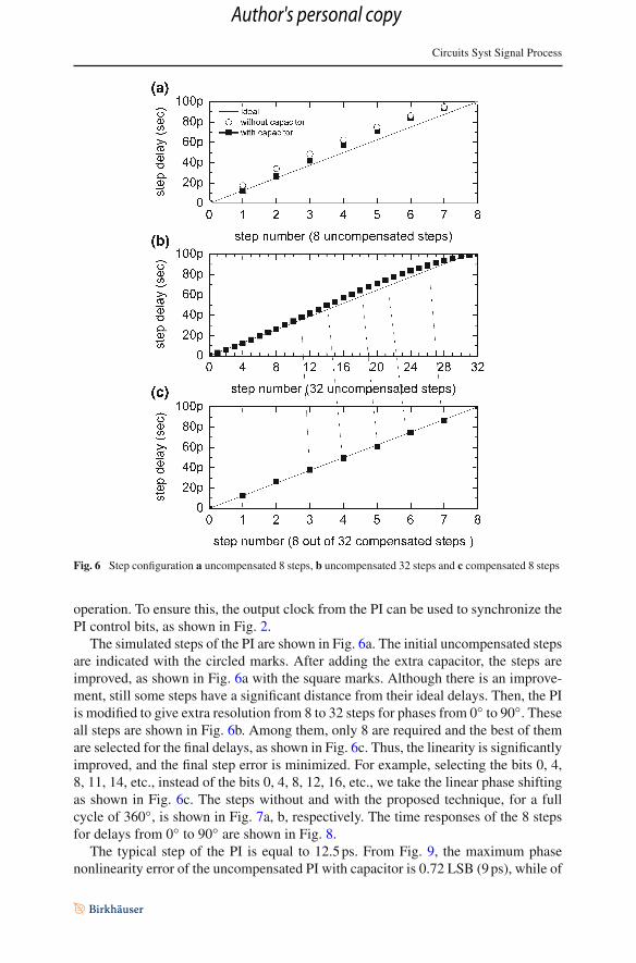
Fig. 6 Step configuration a uncompensated 8 steps, b uncompensated 32 steps and c compensated 8 steps
operation. To ensure this, the output clock from the PI can be used to synchronize thePI control bits, as shown in Fig. 2.
The simulated steps of the PI are shown in Fig. 6a. The initial uncompensated stepsare indicated with the circled marks. After adding the extra capacitor, the steps areimproved, as shown in Fig. 6a with the square marks. Although there is an improve-ment, still some steps have a significant distance from their ideal delays. Then, the PIis modified to give extra resolution from 8 to 32 steps for phases from 0◦ to 90◦. Theseall steps are shown in Fig. 6b. Among them, only 8 are required and the best of themare selected for the final delays, as shown in Fig. 6c. Thus, the linearity is significantlyimproved, and the final step error is minimized. For example, selecting the bits 0, 4,8, 11, 14, etc., instead of the bits 0, 4, 8, 12, 16, etc., we take the linear phase shiftingas shown in Fig. 6c. The steps without and with the proposed technique, for a fullcycle of 360◦, is shown in Fig. 7a, b, respectively. The time responses of the 8 stepsfor delays from 0◦ to 90◦ are shown in Fig. 8.
The typical step of the PI is equal to 12.5ps. From Fig. 9, the maximum phasenonlinearity error of the uncompensated PI with capacitor is 0.72 LSB (9ps), while of
Author's personal copy

Circuits Syst Signal Process
Fig. 7 Step linearity improvement for 360◦ a uncompensated 128 steps, b compensated 32 steps
the compensated PI is less than 0.12 LSB (1.5ps). Monte Carlo simulations performedto estimate the sensitivity on mismatches and device variations. A single typical stepwas simulated for 100 runs with random mismatches and variations, following theGaussian distribution in the range of the mean value of +4 sigma. The expected typicalstep values were 12.5ps, and are in agreement with the results shown in Fig. 10, wherethe mean value was 12.56ps and the standard deviation σ was 0.35ps.
The phase noise of the phase interpolator must be kept low in order to minimize itscontribution to the total noise budget of the system. The phase noise was simulatedsetting the phase interpolator at a locked, constant phase number for each measure-ment. Totally, several steps were simulated to find the phase noise level which wasfound equal to −135dBc/Hz at 1MHz for typical operation conditions. Corner sim-ulation results, presented in Table 1, show that the phase noise kept low in all casesfor slow–slow and fast–fast technology parameters, from −40 to 125◦C temperaturevariations and from 1.08 to 1.32V voltage supply. The worst case for the phase noiseis −131dBc/Hz at fast–fast 1.08V voltage supply and 125◦C temperature.
Author's personal copy

Circuits Syst Signal Process
Fig. 8 0◦–90◦ steps of the PI
Fig. 9 Step error of phase interpolator
The performance of the PI is summarized in Table 2, and in Fig. 11, the layoutis depicted, with some supporting cells. The supporting cells include input CMLmultiplexers, buffers and CML-to-CMOS conversion cells. Also, the extra capacitorsused to improve linearity are shown in this figure. The die area of the core of the PIis 145µm × 35µm, while the total area with the supporting cells, like buffers andCML-to-CMOS converters, is 295µm × 95µm.
A comparison of the performance of the proposed design with other phase inter-polators is presented in Table 3. This table includes only papers which give detailsabout the phase interpolator and not refer to it just as a simple operating block in abigger system. In Table 3, it is presented the typical step, and in the last column, it ispresented the error in ps and the relative error comparing with the typical value. Thephase interpolator in [3,11] runs at low speed, and therefore, the control is easy. In
Author's personal copy

Circuits Syst Signal Process
Fig. 10 Monte carlo results of the step variations
Table 1 Phase noise in several corners
Technology variation Voltage supply (V) Temp. (◦C) Phase noise @ 1MHz
Typical 1.2 27 −135.7
Fast–fast 1.08 −40 −135.5
Fast–fast 1.08 125 −131
Fast–fast 1.32 −40 −136.4
Fast–fast 1.32 125 −132.5
Slow–slow 1.08 −40 −136.5
Slow–slow 1.08 125 −133.9
Slow–slow 1.32 −40 −137.3
Slow–slow 1.32 125 −135.2
Table 2 Performance of PIParameter Value
VDD (V) 1.2
Tech. (nm) 65
Power (mW) 10
Clock (GHz) 2.5
Typical step (ps) 12.5
Step error of a typical step (ps) <1
Area (µm × µm) 145 × 35
[11], several proposed methods improve the phase linearity, which initially was verylow. However, this is a first attempt to create phase interpolation by an accurate way.In [3], although a high-resolution interpolator is proposed, no information is givenabout the error in linearity. High-resolution interpolator is proposed in [7]. Because
Author's personal copy

Circuits Syst Signal Process
Fig.1
1PI
layout
Author's personal copy

Circuits Syst Signal Process
Table3
Com
parisontable
References
Tech.
VDD(V
)Po
wer
(mW)
Clock
(GHz)
Typicalstep(ps)
Step
error(ps),(%)
[1]
0.8µm
3.3
na<0.4
22.5
20.25,
(90%)
[3]
0.25
µm
2.5
na0.12
562
.5na
[7]
130nm
1.2
<10
3.12
53.2
1.2,
(37%)a
[12]
110nm
1.2
na2.5
1.56
1ps,(64
%)b
[2]
65nm
1.2
22.5
56.25
na
[13]
65nm
0.5
nana
>10
00na
[1]
65nm
1.2
na4
20.83
4.51
,(21
%)
613
.88
0.93
,(7%)
[6]
65nm
1na
53.12
50.83
,(27
%)
[9]
130nm
1.2
na1
15.625
na
Thiswork
65nm
1.2
102.5
12.5
1,(8%)a
aInclud
ingmismatch/process
variations
bWorst-casetim
ingequalto8ps
Author's personal copy
Circuits Syst Signal Process
of the high resolution, the absolute step error is improved, but the relative error takesvalues up to 25%. Moreover, high resolution is achieved by feeding the interpolatorwith clocks that have phase difference 30◦, needing extra input clock phases, extra cir-cuits and additional control. Also, in [12], a high-resolution topology is utilized withadditional feedback control of the linearity, showing small nonlinearity error takenby spice simulations and worst-case timing variation 8ps due to 50-mV VDD step.A phase interpolator at 10GHz is presented in [2], but no information about the steperror is provided. In [8], a 0.5V phase interpolator is proposed based on controllingthe slew rate of the output, through controllable inverters. However, this operates atlow speed, probably due to the low supply voltage and needs multiphase oscillator. Ahigh-frequency phase interpolator which tested at 4 and 6GHz is referenced in [1]. Itexhibits an improved performance at 6GHz that is significantly reduced at 4GHz, andtherefore, it must be optimized for each frequency clock. The step resolution, however,is only 30◦ which offers simplicity in terms of design and operation, but on the otherhand, this may be too low for many SerDes systems. In [6], a 5GHz phase interpolatorwith high resolution and 27% worst step error are reported, and a phase interpolatoroperating at 1GHz is given in [9]. Other references are not placed in the table becausethey operate in low speed, which is out the scope of this work or they use the phaseinterpolator as a block without giving specific information about its implementation[5].With regard to Table 3, the proposed phase interpolator shows a good performancefor high-speed clock and improved relative linearity. If required, it could be furtherimproved by using a higher resolution step.
5 Conclusions
A design technique for improving the linearity of analog phase interpolators is pre-sented in this paper. The technique focuses on two main actions: One is by settingsuitable integration of the output signal and second is by creating higher step resolu-tion. The phase interpolator operating at 2.5GHz with a 1.2V voltage supply has beendesigned using a 65nm CMOS technology. The phase error is less than 1ps, and thephase noise is −135dBc/Hz.
References
1. B. Abiri, A. Shivnaraine, R. Sheikholeslami, H. Tamura, M. Kibune, A 1-to-6Gb/s phase-interpolator-based burst-mode CDR in 65 nm CMOS, in Proceedings of Solid-State Circuits Conference Digest ofTechnical Papers. pp. 154–155 (2011)
2. M. Benyahia, J. B. Moulard, F. Badets, A. Mestassi, T. Finateu, L. Vogt, F. Boissieres, A digitallycontrolled 5 GHz analog phase interpolator with 10 GHz LC PLL, in Proceedings of InternationalConference Design & Technology of Integrated Systems in Nanoscale Era. pp. 130–135 (2007)
3. H. Chung, D.-K. Jeong, W. Kim, An 128-phase PLL using interpolation technique. J. Semicond.Technol. Sci. 3(4), 181–186 (2003)
4. B.W. Garlepp, K.S. Donnelly, J. Kim, P.S. Chau, J.L. Zerbe, C. Huang, C. V. Tran, C.L. Portmann, D.Stark, Y.-F. Chan, T.H. Lee, M.A. Horowitz, A portable digital DLL architecture for CMOS interfacecircuits, in Proceedings of 1998 Symposium on VLSI Circuits. Digest of Technical Papers. pp. 214–215(1998)
Author's personal copy

Circuits Syst Signal Process
5. P.K. Hanumolu, G.-Y. Wei, U.-K. Moon, A wide-tracking range clock and data recovery circuit. IEEEJ. Solid State Circuits 43(2), 425–429 (2008)
6. S. Hu, C. Jia, K. Huang, C. Zhang, X. Zheng, Z. Wang, A 10 Gbps CDR based on phase interpolatorfor source synchronous receiver in 65 nm CMOS, in Proceedings of IEEE International SymposiumCircuits Systems. pp. 309–312 (2012)
7. Y. Jiang, A. Piovaccan, A compact phase interpolator for 3.1256G Serdes application, in Proceedingsof Southwest Symposium Mixed-Signal Design. pp. 249–252 (2003)
8. S. Kumakil, A.H. Johari, T. Matsubara, I. Hayashi, H. Ishikurol, A 0.5 V 6-bit scalable phase interpo-lator, in Proceedigs of IEEE Asia Pacific Conference on Circuits and Systems. pp. 1019–1022 (2010)
9. L.N. Li, W.P. Cai, A phase interpolator CDR with low-voltage CML circuits. J. Electron. Sci. Technol.10(4), 314–318 (2012)
10. A. Nicholson, J. Jenkins, A. van Schaik, T.J. Hamilton, T. Lehmann, A 1.2 V 2-bit phase interpolatorfor 65 nm CMOS, in Proceedings of IEEE International Symposium Circuits Systems. pp. 2039–2042(2012)
11. S. Sidiropoulos, M. Horowitz, A semidigital dual delay-locked loop. IEEE J. Solid State Circuits32(11), 1683–1692 (1997)
12. H. Takauchi, H. Tamura, S. Matsubara, M. Kibune, Y. Doi, T. Chiba, H. Anbutsu, H. Yamaguchi, T.Mori, M. Takatsu, K. Gotoh, T. Sakai, T. Yamamura, A CMOSmultichannel 10-Gb/s transceiver. IEEEJ. Solid State Circuits 38(12), 2094–2100 (2003)
13. C.-K.K. Yang, Design of High-Speed Serial Links in CMOS. Technical report: CSL-TR-98-775.Computer Systems Lab, Department of Electrical Engineering and Computer Science, Stanford Uni-versity. http://i.stanford.edu/pub/cstr/reports/csl/tr/98/775/CSL-TR-98-775.pdf (1998). Accessed 20May 2015
Author's personal copy