automated synthesis of wideband bandpass filters based on ... · this paper is focused on the...
TRANSCRIPT

Copyright © 2016 Tech Science Press CMC, Vol.52, No.3, pp.157-172, 2016
Automated Synthesis of Wideband Bandpass Filters Based on Slow-wave EBG Structures
Marco Orellana1, Jordi Selga1, Paris Vélez1, Marc Sans1, Ana Rodríguez2, Vicente Boria2 and Ferran Martín1
Abstract This paper is focused on the automated synthesis of wideband bandpass filters operating at microwave frequencies and based on electromagnetic bandgap (EBG) structures. The classical counterpart of such filter consists of a combination of transmission line sections and shunt-connected grounded stubs placed at equidistant positions. By replacing the transmission line sections with capacitively-loaded lines (a kind of EBG-based lines) exhibiting the same phase shift at the lower cutoff frequency and the same characteristic (actually Bloch) impedance, filter size is reduced and the spurious pass bands can be efficiently suppressed. In practice, the loading capacitances are implemented by means of patches, in order to achieve a fully planar filter implementation. The presence of the patches reduces the effective phase velocity of the capacitively-loaded lines, thus providing a slow-wave effect useful for filter miniaturization. Moreover, due to periodicity, such EBG-based lines exhibit wide stop bands, which are used for spurious suppression. Even though such EBG-based filters were previously reported by some of the authors, a systematic synthesis method was not applied for filter design. In this paper, the main aim is to demonstrate the potential of aggressive space mapping (ASM) for that purpose, and it will be shown that such filters can be automatically synthesized.
Keywords: Electromagnetic bandgaps (EBG), microwave filters, slow-wave transmission lines, space mapping.
1 Introduction
Electromagnetic bandgaps (EBGs), known as photonic bandgaps (PBGs) or photonic crystals at optical frequencies, are periodic structures able to inhibit wave propagation at certain frequencies due to the well known Bragg effect, derived from periodicity [Yablonovitch (1993); Joannopoulos, Meade, and Winn (1995)]. In planar technology, EBG-based structures have been proposed in applications such as microwave reflectors [Qian, Radisic and Itoh (1997); Erro, Laso, Lopetegi, Benito, Garde, and Sorolla (2000); Laso, Lopetegi, Erro, Benito, Garde and Sorolla (2000a); Falcone, Lopetegi, Irisarri, Laso,
1 GEMMA/CIMITEC, Departament d’Enginyeria Electrònica, Universitat Autònoma de Barcelona, 08193 Bellaterra (Barcelona), Spain. 2 Departamento de Comunicaciones-iTEAM, Universitat Politècnica de València, 46022 Valencia, Spain.

158 Copyright © 2016 Tech Science Press CMC, Vol.52, No.3, pp.157-172, 2016
Erro, and Sorolla (1999); Laso, Lopetegi, Erro, Benito, Garde and Sorolla (2000b) ], high-Q resonators [Lopetegi, Falcone and Sorolla (1999); Yun and Chang (2001)], spurious suppression in filters [Lopetegi, Laso, Hernández, Bacaicoa, Benito, Garde, Sorolla and Guglielmi (2001); Lopetegi, Laso, Falcone, Martín, Bonache, Pérez-Cuevas and Sorolla (2004); Martín, Falcone, Bonache, Lopetegi, Laso and Sorolla (2002); Martín, Bonache, Gil, Falcone, Lopetegi, Laso and Sorolla (2004); Martín, Falcone, Bonache, Laso, Lopetegi and Sorolla (2003a)], and harmonic suppression in active circuits [Radisic, Qian, and Itoh (1998); Hang, Radisic, Qian, and Itoh (1999); Yang, Qian, and Itoh (1999); Xue, Shum, and Chan (2001); Lee, Lim, Park, Ahn, and Nam (2002)], among others. In the previous applications, the EBG structures typically consist of transmission lines with ground plane etching (e.g., holes at periodic position), or with modulation of the line width (non-uniform transmission lines). In both cases, stop bands appear at the Bragg frequency, given by
lv
f p
2=
(1) and at its harmonics, where vp is the phase velocity and l is the period of the EBG structure. According to the previous expression, the first stop band occurs at that frequency satisfying that the period is half the wavelength (the rejection level and stopband bandwidth depend on the magnitude of the perturbation and number of periods, and analytical expressions can be found in [Martín (2015)]). Other periodic transmission lines are implemented by loading it with shunt capacitances. Such reactive elements increase the effective capacitance of the line, providing a slow-wave effect that decreases the phase velocity [Görür (1994); Görür, Karpuz and Alkan (1998); Sor, Qian, and Itoh (2001); Nesic (2002); Martín, Falcone, Bonache, Laso, Lopetegi and Sorolla (2003b); Martín, Bonache, Gil, Falcone, Lopetegi, Laso and Sorolla (2004); Kaddour, Issa, Franc, Corrao, Pistono, Podevin, Fournier, Duchamp, and Ferrari (2009); Franc, Kaddour, Issa, Pistono, Corrao, Fournier and Ferrari (2010); Abdel Aziz, Issa, Kaddour, Podevin, Safwat, Pistono, Duchamp, Vilcot, Fournier, and Ferrari (2012)]. Thus, capacitively loaded EBG-based lines behave as slow-wave transmission lines with stopbands related to periodicity. According to this, such artificial lines can be useful to simultaneously reduce device size in planar microwave circuits and to suppress spurious bands, inherent to distributed circuits. To avoid the presence of lumped elements (with the corresponding penalty in terms of cost and fabrication complexity), capacitively loaded lines have been typically implemented by means of patch capacitances or with other planar geometries that effectively increase the line capacitance [Orellana, Selga, Sans, Rodríguez, Boria, and Martín (2015)]. In the field of microwave filters these slow-wave structures have been used to reduce size and improve the stopband response (by suppressing the spurious bands) [Martín, Bonache, Gil, Falcone, Lopetegi, Laso and Sorolla (2004); García-García, Bonache and Martín (2006)]. In the present paper, we deal with capacitively loaded EBG transmission lines, applied to the design of a class of bandpass filters able to provide wide pass bands but wide spurious bands as well. By replacing part of the distributed elements (transmission line sections) with patch loaded lines, the spurious bands can be substantially rejected, as will be shown
Automated Synthesis of Wideband Bandpass Filters Based 159
later. Moreover, filter length is also reduced by the above-mentioned slow-wave effect. This idea was already proposed by some of the authors [García-García, Bonache and Martín (2006)]. Here, the main focus is to provide an automated and systematic synthesis procedure for such EBG-based filters relying on space mapping optimization [Bandler, Biernacki, Chen, Grobelny and Hemmers (1994)], and particularly using quasi-Newton type iteration (namely, implementing an iterative algorithm based on the so-called aggressive space mapping -ASM- [Bandler, Biernacki, Chen, Hemmers, and Madsen (1995)]). The paper is organized as follows. In section 2, the topology and design of the classical (i.e., EBG-less) filters considered in this work are presented. Section 3 is focused on the considered slow-wave structures. In section 4, the general formulation of ASM is presented for coherence and completeness. In section 5, the ASM is applied to the synthesis of the slow-wave structures necessary to suppress the spurious bands of the filter and reduce device size. Section 6 presents the results, including measurements. Finally, the main conclusions are highlighted in section 7.
2 Wideband Bandpass Filters Based on Shunt Stubs: Topology and Design
Let us first briefly review the topology and design of the wideband (EBG-less) filters in which the proposed EBG-based filters of this work are inspired. Such filters consist of a cascade of shunt stubs of equal length, alternating with transmission lines of twice the stub electrical length. The analysis of this type of filters was done by Levy [Levy (1970)]. By using n stubs, an insertion function of degree 2n−1 is implemented in these filters, which are useful to generate wide transmission bands. However, wideband spurious are also present in their frequency response. The schematic of the filter is depicted in Fig. 1. The network shown in Fig. 1 implements the transfer function described in expression (2a) as a function of the normalized frequency variable θ = θc f/fc [Hong and Lancaster (2001)]:
)(11)( 22
221 θκθ
nFS
+=
(2a) with
( ) ( )
2cos −
−−−
−+
=−−
θπθ
2
·11·11)(
322
122
cnc
cnc
n
xxTx
xxTx
F
(2b)
−= θπ
2sinx
(2c)
−= ccx θπ
2sin
(2d)

160 Copyright © 2016 Tech Science Press CMC, Vol.52, No.3, pp.157-172, 2016
where ( ))xTn = cos(ncos−1 and κ is the pass band ripple constant. The bandwidth of the and κ is the pass band ripple constant. The bandwidth of the filter is delimited by the frequencies fc and (π/θc−1)fc; therefore, the bandwidth can be controlled by the value of the angle θc . The impedance values of the short-circuit stubs and line elements can be chosen for optimum distributed highpass filters according to tabulated element values supplied e.g. in ref. [Hong and Lancaster (2001)].
Figure 1: Schematic of the wideband bandpass filter where yi and yjk are the normalized characteristic admittances of the stubs and transmission lines, respectively.
3 Slow-wave Structures Based on Capacitively-loaded Line
As mentioned before, the filters considered in the previous section exhibit wide spurious bands, and the first one is close to the band of interest. Such spurious can be eliminated by loading the line sections with patch capacitors [García-García, Bonache and Martín (2006)]. The effect of the capacitances in the line sections is twofold: (i) stop bands appear in the transmission spectrum of these line sections as consequence of periodicity; (ii) the phase velocity is reduced since the effective capacitance per unit length of the line increases. Thus, by loading the line sections with the patch capacitors, not only the filter spurious can be suppressed, but also the filter length can be reduced. Even though the main interest in this paper is to present an automated synthesis method for these capacitively-loaded filters, let us first briefly review the analysis of these capacitively-loaded lines. In a transmission line periodically loaded with shunt connected capacitances (Fig. 2a), the dispersion relation is [Orellana, Selga, Sans, Rodríguez, Boria, and Martín (2015)]:
klZCkll ols sin2
coscos ωβ −= (3)
where k and β are the phase constants of the unloaded and loaded line, respectively, Cls are the loading capacitances, l is the distance between adjacent capacitances (period) and Zo is the characteristic impedance of the line sections between adjacent capacitances. According to this dispersion relation, the structure exhibits a low pass filter type response with multiple spurious bands (or multiple stop bands). For design purposes, however, a lumped element circuit model of the capacitively loaded transmission line is convenient. This circuit model is depicted in Fig. 2(b), where C and L are the per-section capacitance and inductance of the line, respectively. This model is valid under the assumption that Cls >> C. According to the lumped element equivalent circuit of the periodically loaded

Automated Synthesis of Wideband Bandpass Filters Based 161
line, the first pass band of the structure is delimited by the following cut-off frequency
[Martín (2015)]
)(1
lsB CCL
f+
=π (4)
the characteristic (or Bloch) impedance of the loaded line at low frequencies is given by
lsB CC
LZ+
= (5)
and the lower frequency of the first spurious band is
LCfS 2
1=
(6) The slow-wave factor, defined as the ratio between the phase velocity of the loaded and unloaded line is given by
CCLCl
CCLlvv
swrls
ls
po
p
+=
+==
1
1/
)(/
(7) and the electrical length of the unit cell (3) at low frequencies, i.e., far enough from the Bragg frequency, can be approximated by
( )Cell lsl L C Cφ β ω= = + (8) Even though the previous equations are approximate, they are useful for design purposes.
Figure 2: Schematic of the slow-wave structure based on a capacitively loaded line (a), and lumped element equivalent circuit model (b).

162 Copyright © 2016 Tech Science Press CMC, Vol.52, No.3, pp.157-172, 2016
Note that the number of variables of the circuit model of Fig. 2(b) is three; hence three conditions are needed to determine these element values. The characteristic impedance (expression 5) is one of these conditions, directly dictated from filter specifications. The second one is given by (8), since we must set the phase shift per cell at a given frequency, for instance fc. Inspection of (5) and (8) reveals that these two conditions determine univocally L and C + Cls. To infer C and Cls, the slow-wave factor (7) was used in [Martín (2015)] as an additional condition. Alternatively, (6) can be used if, rather than the reduction of the line length, the main interest is the control of the stopband bandwidth (note that expression 6 provides the upper limit of the stop band). An important aspect to be considered in the present application of these capacitively-loaded lines concerns the position of the first cutoff frequency, given by (4). This frequency must be forced to be between the first filter pass band (i.e., the band of interest) and the first spurious band; otherwise, either the first spurious is not efficiently suppressed, or the filter cutoff frequency is decreased. However, note that fB is determined from the phase of the unit cell at the considered frequency (expression 8). From (4) and (8), it follows:
B
ccell f
f2=φ
(9) Since the upper limit of the filter pass band and the lower limit of the first spurious bands are given by (π/θc−1)fc and (π/θc+1)fc, it follows that the phase shift per cell is limited by the following values:
c
ccell
c
c
θπθφ
θπθ
−<<
+22
(10) Now, let us assume that the number of cells of each transmission line section is N. This means that φcell = 2θc/N at fc, or
cc N θπθπ +<<− (11) Thus, according to this analysis, N cannot be arbitrary, and the possible values are dictated by θc.
4 General Formulation of ASM
The expressions (5) and (8) are approximate and therefore, optimization of the patch loaded lines is necessary. Indeed, it is first necessary to find the schematic of such lines (Fig. 2a) providing exactly the required values of Bloch impedance and phase shift, and once this schematic is determined, the next step is the determination of the layout of such artificial lines. Following our previous work [Orellana, Selga, Sans, Rodríguez, Boria, and Martín (2015)], we have implemented two aggressive space mapping (ASM) algorithms; the first one provides the schematic; the second one generates automatically the layout. Our hypothesis is that, once the layouts of the capacitvely loaded transmission line sections are determined, the layout of the filter is simply constructed by cascading these artificial transmission line sections with the shunt stubs, also subjected to a simple ASM optimization algorithm.

Automated Synthesis of Wideband Bandpass Filters Based 163
For completeness, let us briefly review the general formulation of ASM. In ASM, two simulation spaces are considered [Bandler, Biernacki, Chen, Grobelny and Hemmers (1994); Bandler, Biernacki, Chen, Hemmers, and Madsen (1995)]: (i) the optimization space, Xc, where the variables are linked to a coarse model, which is simple and computationally efficient, although not accurate, and (ii) the validation space, Xf, where the variables are linked to a fine model, typically more complex and CPU intensive, but significantly more precise. In each space, a vector containing the different model parameters can be defined. Let us call such vectors xf and xc in the fine and coarse model spaces, respectively, and let us designate by Rf(xf) and Rc(xc) their corresponding responses. The goal in ASM is to minimize the error function in (12) following a quasi-Newton iterative process.
*cff xxPxf −= )()( (12)
where xc* is the coarse model solution that gives the target response, Rc(xc
*), and P(xf) is a parameter extraction function that gives the parameters of the coarse model from those of the fine model. Let us assume that xf
( j ) is the j-th approximation to the solution in the validation space, and f( j ) the error function corresponding to f(xf
( j )). The next vector of the iterative process xf
( j+ 1) is obtained according to )()()1( jjj hxx ff +=+
(13) where h( j) is given by:
( ) )(1)()( jjj fBh −−= (14)
and B(j) is an approximate to the Jacobian matrix which is also updated by a simplification of the classical Broyden formula [Bandler, Biernacki, Chen, Hemmers, and Madsen (1995); Broyden (1965)] at each iterative step.
)()(
)()1()()1(
jTj
Tjjjj
hhhfBB
++ +=
(15) In (15), f( j+1) is obtained by evaluating (12) using a certain parameter extraction method providing the coarse model parameters from the fine model parameters, and the super-index T stands for transpose. In the next section, the new proposed two-step ASM synthesis algorithm is explained in detail.
5 The ASM Algorithm The specific ASM algorithm for the synthesis of the capacitively-loaded transmission line sections was first presented in [Orellana, Selga, Sans, Rodríguez, Boria, and Martín (2015)]. It was divided in two steps: (i) the determination of the optimum schematic, providing the required specifications, and (ii) the generation of the layout. The first step is necessary since expressions (5) and (8) are approximate. The variables of the coarse space are the three specifications: Bloch impedance, ZB, electrical length per unit cell, βl, and slow-wave ratio, swr. The response of these variables in the coarse space is simply given by the electrical simulation of the circuit of Fig. 2(b) with the element values

164 Copyright © 2016 Tech Science Press CMC, Vol.52, No.3, pp.157-172, 2016
inferred from expressions (5), (7) and (8). The variables of the fine model are Zo, kl and Cls, and the response of this model is given by the circuit simulation of the schematic of Fig. 2(a). To initiate this first ASM, we must provide the values of the variables of the fine model according to some criterion. The most straightforward one is to identify Cls with the value of this variable inferred by isolation of (5), (7) and (8). The values of C and L also provide Zo, i.e.,
CLZo =
(16) and kl, given by:
LCkl ω= (17) Once the variables of the fine model are determined, the response is obtained by circuit simulation of the schematic (Fig. 2a). From this response (or from analytical expressions provided in [Orellana, Selga, Sans, Rodríguez, Boria, and Martín (2015)]), we extract the variables of the coarse model corresponding to the first iteration xc
(1). Then, we compare such values with the target (xc
*) and this gives the first error function (12). After that, the matrix B must be calculated. To obtain the first approximation to this matrix, we slightly perturb each variable of the fine model from the first value inferred as indicated above. Then we obtain the circuit response, and from it we obtain the resulting variables of the coarse model corresponding to each perturbation. The relative changes can be expressed in a matrix form as follows:
(1)B
B B B
o ls
o ls
o ls
Z Z ZZ kl C
l l lZ kl C
swr swr swrZ kl C
δ δ δδ δ δδβ δβ δβδ δ δδ δ δδ δ δ
= (18)
which corresponds to the initial matrix B. Once the matrix B(1) is known, the fine model parameters of the following iteration can be derived from (14), and the process is iterated until convergence is obtained. Once the schematic is determined, layout synthesis is achieved by considering a specific ASM algorithm where the dimension of the (square) patch capacitor and the host line length are determined independently (the host line width is not considered an optimization variable since the analytical formulas are very accurate). The specific procedure, detailed in [Orellana, Selga, Sans, Rodríguez, Boria, and Martín (2015)], involves thus two independent sub-ASM processes. Once the layouts of the capacitively-loaded line sections are determined, determination of the layout of the shunt stubs is required to complete the filter synthesis. However, this last step is simple since only optimization of the stub length is necessary.
Automated Synthesis of Wideband Bandpass Filters Based 165
6 Results
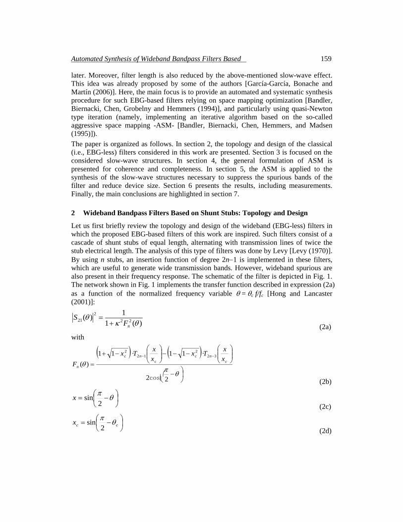
To demonstrate the potential of the proposed ASM scheme, let us consider as an example the synthesis of a filter with the following specifications: fc = 1 GHz, bandwidth BW = 3 GHz, and 3 stubs (i.e., n = 3). With these filter parameters, the electrical length of the stubs is found to be θc = 36o, and that of the transmission line sections is, hence, 2θc = 72o. The characteristic impedances of the transmission line sections and stubs, as well as their lengths and widths, are indicated in Fig. 3(a), corresponding to the topology of the conventional implementation (the Rogers RO4003C substrate with thickness h = 0.813 mm and dielectric constant εr = 3.55 is considered). Fig. 3(b) depicts the simulated frequency response, where the presence of the spurious band, close to the band of interest, can be appreciated (the electromagnetic simulation has been carried out by means of Keysight Momentum and the response of the schematic by means of the circuit simulator of Keysight ADS).
Figure 3: Layout of the conventional filter of the reported example (a) and simulated frequency response (b).
166 Copyright © 2016 Tech Science Press CMC, Vol.52, No.3, pp.157-172, 2016
Let us now replace the transmission line sections of characteristic impedance 48.59 Ω with capacitively-loaded slow wave transmission lines. The considered slow wave factor is swr = 0.5. According to (11) and the value of θc, the number of cells of the transmission lines must be set to N = 3. Therefore, φcell = βl = 24o. According to these values, inversion of expressions (5), (7) and (8) provides the following element values for the circuit of Fig. 2(b): C = 0.34 pF, Cls = 1.03 pF and L = 3.24 nH. From equations (16)-(17), the values of the first iteration of the fine model, xf
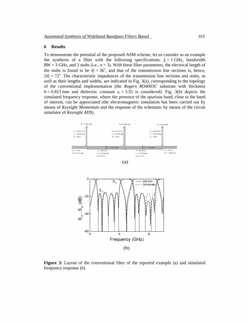
(1) are: Zo = 97.18 Ω, kl = 12.0o, and Cls = 1.03 pF. Using the first ASM algorithm, we have determined the optimum schematic. Convergence, with a relative error of 0.09%, has been achieved after 2 iterations. The resulting values of the fine model are Zo = 98.28 Ω, kl = 12.0o, and Cls = 1.01 pF. The electrical length and characteristic impedance of the schematic (unit cell) using the previous values of the fine model parameters is depicted in Fig. 4. The frequency response that results by cascading three cells is shown in Fig. 5. In view of these figures, at schematic level the resulting electrical length at fc, Bloch impedance and slow-wave factor of the cell after convergence are found to be ZB = 48.62 Ω, φcell = 23.99o and swr = 0.50, respectively.
Figure 4: Characteristic impedance (a) and electrical length (b) of the synthesized unit cell.

Automated Synthesis of Wideband Bandpass Filters Based 167
Figure 5: Frequency response of the synthesized artificial transmission line consisting of three cells.
Once the optimum schematic has been obtained, the application of the second ASM has led us to the layout (unit cell) depicted in Fig. 6. The response of this structure, considering three cells, inferred from electromagnetic simulation using the Keysight Momentum commercial simulator, is also depicted in Fig. 5, and reveals that the Bragg frequency lies between the upper cutoff frequency of the first pass band and the lower cutoff frequency of the spurious band. There is some discrepancy between the response of the schematic and the one inferred from electromagnetic simulation due to the fact that the model of the patch capacitors is valid at low frequencies (such discrepancies can be also appreciated in Fig. 4). Nevertheless, the Bragg frequency obtained from electromagnetic simulation has the correct value, and a huge stop band, useful for the suppression of the spurious band of the filter, results.
Figure 6: Layout of the unit cell. Dimensions are: l = 6.767 mm, lp = 4.282 mm, Wacc = 2.141 mm (0.5lp), lacc = 0.583 mm, Whost = 0.475 mm

168 Copyright © 2016 Tech Science Press CMC, Vol.52, No.3, pp.157-172, 2016
By cascading three unit cells, we have constructed the capacitively-loaded transmission line sections of the filter. The final layout of the filter is depicted in Fig. 7(b), where it is compared to the conventional one in Fig. 7(a). The responses (inferred from lossless electromagnetic simulation) are compared in Fig. 7(c). The filter has been fabricated by means of a LPKF-H100 drilling machine and has been characterized by means of the Agilent E8364B vector network analyzer. The photograph of the prototype is depicted in Fig. 8(a), whereas Fig. 8(b) depicts the measured frequency response compared to the one inferred from electromagnetic simulation (including losses). Thanks to the presence of the capacitively loaded lines, significant attenuation of the spurious band (better than 36 dB up to 10 GHz) is achieved.
Figure 7: Layout of the conventional filter (a), layout of the synthesized EBG loaded filter (b), and simulated frequency response of both filters (c). Dimensions are indicated.

Automated Synthesis of Wideband Bandpass Filters Based 169
Figure 8: Photograph of the fabricated filter (a) and frequency response (b).
7 Conclusions
In summary, it has been demonstrated that aggressive space mapping (ASM) optimization can be applied to the synthesis of wideband bandpass filters based on capacitively-loaded electromagnetic bandgap (EBG) transmission lines. A systematic design approach, based on a two-step ASM iterative algorithm, where first the optimum circuit schematic is determined, and then the filter layout is generated, has been presented. Thanks to the slow wave effect of the capacitively loaded lines, significant compactness, as compared to the conventional filter implementation, has been achieved. Moreover, the designed filter is spurious free up to high frequencies due to the reflection properties of the EBG-based transmission lines.

170 Copyright © 2016 Tech Science Press CMC, Vol.52, No.3, pp.157-172, 2016
Acknowledgement This work has been supported by MINECO (Spain) under projects TEC2013-40600-R and TEC2013-49221-EXP, by AGAUR-Generalitat de Catalunya under project 2014SGR-157, and by FEDER funds. Ferran Martín is in debt to Institució Catalana de Recerca i Estudis Avançats (ICREA) for supporting his work. Marco Orellana acknowledges the support of the Universidad de Costa Rica, MICITT and CONICIT to study at the Univesitat Autònoma de Barcelona.
References
Abdel Aziz, M.; Issa, H.; Kaddour, D.; Podevin, F.; Safwat, A.M.E.; Pistono, E.; Duchamp, J.-M.; Vilcot, A.; Fournier, J.-M.; Ferrari, P. (2012): Slow-wave high-Q coplanar striplines in CMOS technology and their RLCG model, Microw. Opt. Techn. Lett., vol. 54, pp. 650-654. Bandler, J.W.; Biernacki, R.M.; Chen, S.H.; Grobelny, P.A.; Hemmers, R.H. (1994): Space mapping technique for electromagnetic optimization, IEEE Trans. Microw. Theory Tech., vol. 42, pp. 2536-2544. Bandler, J.W.; Biernacki, R.M.; Chen, S.H.; Hemmers, R.H.; Madsen, K. (1995): Electromagnetic optimization exploiting aggressive space mapping, IEEE Trans. Microw. Theory Tech., vol. 43, pp. 2874-2882. Broyden, C. G. (1965): A Class of Methods for Solving Nonlinear Simultaneous Equations, Mathematics of Computation, vol. 19, no. 92, pp. 577-593. Erro, M. J.; Laso, M. A. G.; Lopetegi, T.; Benito, D.; Garde, M. J.; Sorolla, M. (2000): Optimization of tapered bragg reflectors in microstrip technology, Int. J. Infrared Millimeter Waves, vol. 21, pp. 231- 245. Falcone, F.; Lopetegi, T.; Irisarri, M.; Laso, M. A. G.; Erro, M. J.; Sorolla, M. (1999): Compact photonic bandgap microstrip structures, Microw. Opt. Techn. Lett., vol 23, pp. 233-236. Franc, A.-L.; Kaddour, D.; Issa, H.; Pistono, E.; Corrao, N.; Fournier, J.-M.; Ferrari, P. (2010): Impact of technology dispersion on slow-wave high performance shielded CPW transmission lines characteristics, Microw. Opt. Techn. Lett., vol. 52, pp. 2786, 2789. García-García, J.; Bonache, J.; Martín, F. (2006): Application of electromagnetic bandgaps (EBGs) to the design of ultra wide band pass filters (UWBPFs) with good out-of-band performance, IEEE Trans. Microw. Theory Tech., vol. 54, pp. 4136-4140. Görür, A. (1994): A novel coplanar slow-wave structure, IEEE Microw. Guided Wave Lett., vol. 4, pp. 86–88. Görür, A.; Karpuz, C.; Alkan, M. (1998): Characteristics of periodically loaded CPW structures, IEEE Microw. Guided Wave Lett., vol. 8, pp. 278-280. Hang, C. Y.; Radisic, V.; Qian, Y.; Itoh, T. (1999): High efficiency power amplifier with novel PBG ground plane for harmonic tuning, IEEE MTT-S Int. Microw. Symp. Dig., Anaheim, CA, June 1999, pp. 807-810. Hong, J.-S.; Lancaster, M.L. (2001): Microstrip Filters for RF/Microwave Applications, New York, John Wiley.
Automated Synthesis of Wideband Bandpass Filters Based 171
Joannopoulos, J. D.; Meade, R. D.; Winn, J. N. (1995): Photonic Crystals: Molding the Flow of Light, Princeton, NJ, Princeton University Press. Kaddour, D.; Issa, H.; Franc, A.-L.; Corrao, N.; Pistono, E.; Podevin, F.; Fournier, J.-M.; Duchamp, J.-M.; Ferrari, P. (2009): High-Q slow-wave coplanar transmission lines on 0.35-μm CMOS process, IEEE Microw. Wireless Compon. Lett., vol. 19, pp. 542-544. Laso, M. A. G.; Lopetegi, T.; Erro, M. J.; Benito, D.; Garde, M. J.; Sorolla M. (2000): Multiple-frequency-tuned photonic bandgap microstrip structures, IEEE Microw. Guided Wave Lett., vol. 10, pp. 220-222. Laso, M. A. G.; Lopetegi, T.; Erro, M. J.; Benito, D.; Garde, M. J.;Sorolla, M. (2000): Novel wideband photonic bandgap microstrip structures, Microw. Opt. Techn. Lett., vol. 24, pp. 357-360. Lee, Y. T.; Lim, J. S.; Park, J. S.; Ahn, D.; Nam, S. (2002): A novel phase noise reduction technique in oscillators using defected ground structure, IEEE Microw. Wireless Compon. Lett., vol. 12, pp. 39-41. Levy, R. (1970): A new class of distributed prototype filters with applications to mixed lumped/distributed component design, IEEE Trans. Microw. Theory Tech., vol. 18, pp. 1064-1071. Lopetegi, T.; Falcone, F.; Sorolla, M. (1999): Bragg reflectors and resonators in microstrip technology based on electromagnetic crystal structures, Int. J. Infrared Millimeter Waves, vol. 20, pp. 1091-1102. Lopetegi, T.; Laso, M.A.G.; Hernández, J.; Bacaicoa, M.; Benito, D.; Garde, M.J.; Sorolla, M.; Guglielmi, M. (2001): New microstrip wiggly-line filters with spurious passband suppression, IEEE Trans. Microw. Theory Tech., vol. 49, pp 1593-1598. Lopetegi, T.; Laso, M.A.G.; Falcone, F.; Martín, F.; Bonache, J.; Pérez-Cuevas, L.; Sorolla, M. (2004): Microstrip wiggly line band pass filters with multispurious rejection, IEEE Microw. Wireless Compon. Lett., vol. 14, pp.531-533. Martín, F.; Falcone, F.; Bonache, J.; Lopetegi, T.; Laso, M.A.G.; Sorolla, M. (2002): New periodic-loaded electromagnetic bandgap coplanar waveguide with complete spurious passband suppression, IEEE Microw. Wireless Compon. Lett., vol. 12, pp. 435-437. Martín, F.; Falcone, F.; Bonache, J.; Laso, M.A.G.; Lopetegi, T.; Sorolla, M. (2003): Dual electromagnetic bandgap CPW structures for filter applications, IEEE Microw. Wireless Compon. Lett., vol. 13, pp. 393-395. Martín, F.; Falcone, F.; Bonache, J.; Laso, M.A.G.; Lopetegi, T.; Sorolla, M. (2003): New CPW low pass filter based on a slow wave structure, Microw. Opt. Techn. Lett., vol. 38, pp. 190-193. Martín, F.; Bonache, J.; Gil, I.; Falcone, F.; Lopetegi, T.; Laso, M.A.G.; Sorolla, M. (2004): Compact spurious free CPW band pass filters based on electromagnetic bandgap structures, Microw. Opt. Techn. Lett, vol. 40, pp. 146-148. Martín, F. (2015): “Artificial Transmission Lines for RF and Microwave Applications”, John Wiley, Hoboken, NJ.

172 Copyright © 2016 Tech Science Press CMC, Vol.52, No.3, pp.157-172, 2016
Nesic, D. (2002): A new type of slow-wave 1-D PBG microstrip structure without etching in the ground plane for filter and other applications, Microw. Opt. Techn. Lett., vol. 33, pp. 440-443. Orellana, M.; Selga, J.; Sans, M.; Rodríguez, A.; Boria, V.; Martín, F. (2015): Synthesis of slow-wave structures based on capacitive-loaded lines through aggressive space mapping (ASM), International Journal of RF and Microwave Computer-Aided Engineering, vol. 25, pp. 629-638. Qian, Y.; Radisic, V.; Itoh, T. (1997): Simulation and experiment of photonic band-gap structures for microstrip circuits, Proc. Asia-Pacific Microwave Conf., Hong Kong, Dec. 1997, pp. 585-588. Radisic, V.; Qian, Y.; Itoh, T. (1998): Broad-band power amplifier using dielectric photonic bandgap structure, IEEE Microw. Guided Wave Lett., vol. 8, pp. 13-14. Sor, J.; Qian, Y.; Itoh, T. (2001): Miniature low-loss CPW periodic structures for filter applications, IEEE Trans. Microw. Theory Tech., vol. 49, pp. 2336-2341. Xue, Q.; Shum, K. M.; Chan, C. H. (2001): Novel oscillator incorporating a compact microstrip resonant cell, IEEE Microw. Wireless Compon. Lett., vol. 11, pp. 202-204. Yablonovitch, E. (1993): Photonic band gap structures, J. Opt. Soc. Amer. B 10, pp. 283-295. Yang, F. R.; Qian, Y.; Itoh, T. (1999): A novel uniplanar compact PBG structure for filter and mixer applications, IEEE MTT-S Int. Microw. Symp. Dig., Anaheim, CA, June 1999, pp. 919-922. Yun, T-Y.; Chang, K. (2001): Uniplanar one-dimensional photonic-bandgap structures and resonators, IEEE Trans. Microw. Theory Tech., vol. 49, pp. 549-553.