automatic clock abstraction from sequential circuits · pdf fileautomatic clock abstraction...
TRANSCRIPT
CARNEGIE MELLONDepartment of Electrical and Computer Engineering~
Automatic Clock Abstractionfrom Sequential Circuits
Samir Jain
1994
Advisor: Prof. Bryant
Automatic Clock Abstraction from Sequential Circuits
Samir Jain
Department of Electrical and Computer Engineering
Carnegie Mellon University
Pittsburgh, Pennsylvania 15213
November 1994
Submitted in partial fulfillment of the requirements for the degree of Master of Science in
Electrical and Computer Engineering.

Acknowledgments
First and foremost, I would like to thank my advisor, Randy Bryant, for providing such an interest-
ing research topic. Randy’s guidance and suggestions during our weekly meetings were invalu-
able.
Alok Jain served as my mentor for the project, but was really more of a second advisor. Without
his daily teaching and advice, I never would have been able to complete this project.
Sari Coumeri and Shailavi Shah both proofread my thesis, for which I am grateful. Sari’s feedback
of my technical details was insightful and beneficial. Shailavi provided daily moral support and
reminded me that there are other things in life outside of research.
Finally, I would like to thank my family, simply for being my family. They have offered me end-
less amounts of support, encouragement, and love.
Abstract
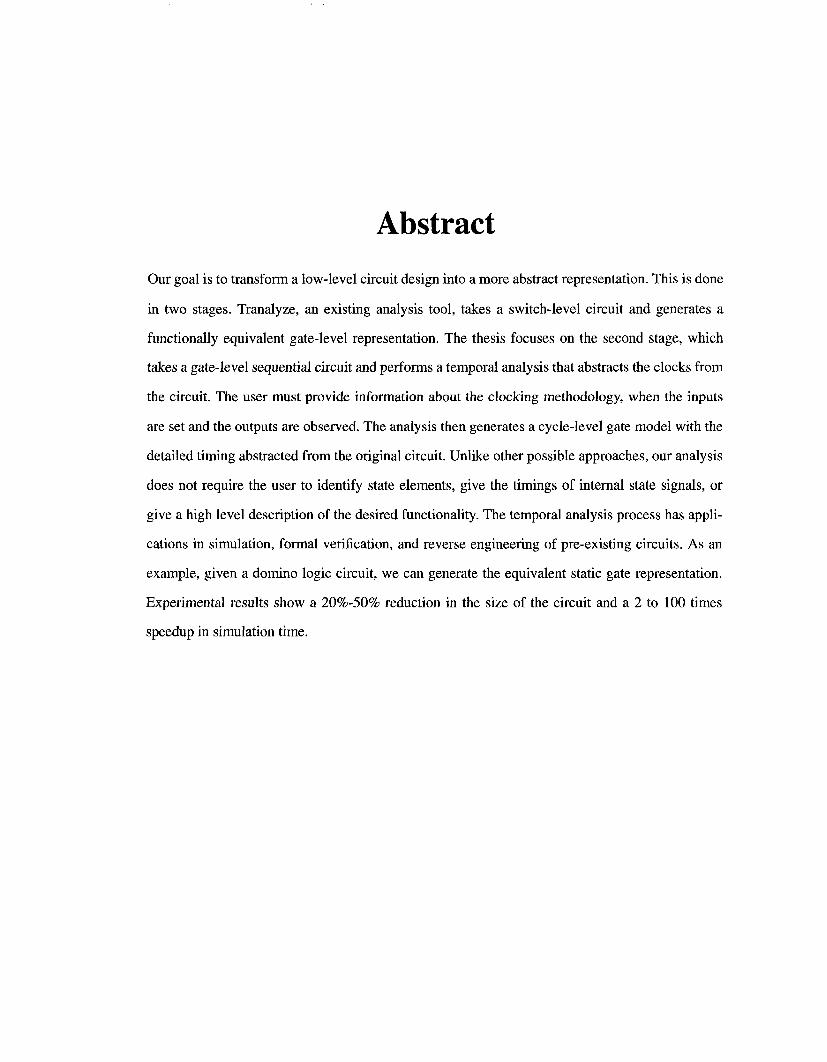
Our goal is to transform a low-level circuit design into a more abstract representation. This is done
in two stages. Tranalyze, an existing analysis tool, takes a switch-level circuit and generates a
functionally equivalent gate-level representation. The thesis focuses on the second stage, which
takes a gate-level sequential circuit and performs a temporal analysis that abstracts the clocks from
the circuit. The user must provide information about the clocking methodology, when the inputs
are set and the outputs are observed. The analysis then generates a cycle-level gate model with the
detailed timing abstracted from the original circuit. Unlike other possible approaches, our analysis
does not require the user to identify state elements, give the timings of internal state signals, or
give a high level description of the desired functionality. The temporal analysis process has appli-
cations in simulation, formal verification, and reverse engineering of pre-existing circuits. As an
example, given a domino logic circuit, we can generate the equivalent static gate representation.
Experimental results show a 20%-50% reduction in the size of the circuit and a 2 to 100 times
speedup in simulation time.
TABLE OF CONTENTS
Introduction 1
1.11.2
1.3
1.4
1.5
Background and Motivation ................................................................................................ 1Domino Example .................................................................................................................3Previous Work ......................................................................................................................51.3.1 Clock Suppression ................................................................................................. 51.3.2 Other methods ....................................................................................................... 7
Our Approach .......................................................................................................................7
Organization of the M.S. report ........................................................................................... 8
Clock Abstraction 9
2.1 Discrete Timing Model ........................................................................................................ 92.1.1 Basic Model ...........................................................................................................92.1.2 Timing Specifications .......................................................................................... 112.1.3 Detailed Model ....................................................................................................12
2.2 Temporal Analysis Algorithm ............................................................................................ 142.2.1 Presimulation algorithm ...................................................................................... 142.2.2 Core Temporal Analysis algorithm ..................................................................... 152.2.3 Cycle delays .........................................................................................................16
2.3 Examples ............................................................................................................................162.3.1 Delay Flip-flop ..................................................................................................... 162.3.2 Mead and Conway Stack ..................................................................................... 21
Implementation 27
3.1 Tranalyze ............................................................................................................................273.1.1 Logic States .........................................................................................................273.1.2 Gate Primitives ....................................................................................................283.1.3 3-input nand example .......................................................................................... 293.1.4 Redundancy check ...............................................................................................303.1.5 Unit delays ...........................................................................................................313.1.6 Domino Example ................................................................................................. 32
3.2 Symbolic Simulation ..........................................................................................................333.2.1 Delay models .......................................................................................................343.2.2 Binary Decision Diagrams .................................................................................. 343.2.3 Types of Simulation .............................................................................................35
Results 374.1
4.2
4.3
Tranalyze vs. COSMOS ..................................................................................................... 37
Redundancy Check ............................................................................................................39Temporal Analysis .............................................................................................................41
Conclusions and Future Work 44Bibliography 46
Section 1
Introduction
1.1 Background and Motivation
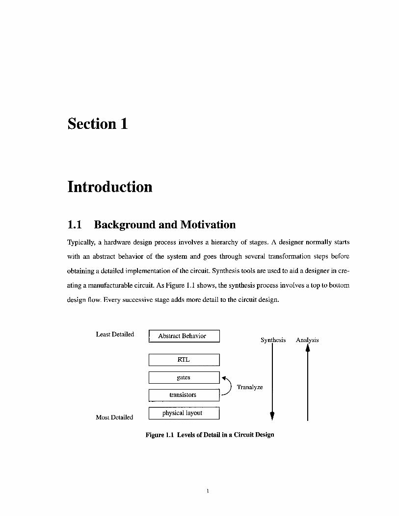
Typically, a hardware design process involves a hierarchy of stages. A designer normally starts
with an abstract behavior of the system and goes through several transformation steps before
obtaining a detailed implementation of the circuit. Synthesis tools are used to aid a designer in cre-
ating a manufacturable circuit. As Figure 1.1 shows, the synthesis process involves a top to bottom
design flow. Every successive stage adds more detail to the circuit design.
Least Detailed [ Abstract Behavior
gates
transistors
Most Detailed I physical lay°ut
Tranalyze
Synthesis Anal’ ~sis
Figure 1.1 Levels of Detail in a Circuit Design
While synthesis tools help a designer create a manufacturable circuit, there exists a need for tools
that transform detailed circuit models into more abstract, less complicated models. This process,
also shown in Figure 1.1, is a bottom to top flow. A more abstract circuit design may provide
advantages in the areas of simulation, formal hardware verification, and reverse engineering of
existing circuits. As designs grow larger, it becomes impractical to simulate an entire low-level
design. Transformations are performed to remove details from the circuit design, thus producing a
smaller abstracted circuit and improving the performance of a simulator. The task of formal verifi-
cation is to verify that a circuit functions according to its abstract specification. Typically, there is a
wide gap between a detailed circuit and its specification. Tools that move a circuit up the design
chain allow us to reduce this gap. Finally, there has been a recent interest in being able to reverse
engineer an existing circuit design. As the design industry matures, old circuit designs are uncov-
ered in which the functionality of the circuit is unknown or lost. The circuits may have compli-
cated clocking and timing patterns, making them difficult to understand. Performing a temporal
analysis will abstract out the timing, thus enabling the user to understand the functionality.
A tool called Tranalyze [9] has been created that transforms a switch-level circuit into a function-
ally equivalent gate-level representation. However, this circuit generated from the switch-level
analysis is still a very low-level representation. If the clocking methodology is known, the clocks
can be abstracted through a "temporal analysis" that would generate a higher-level circuit, as
shown in Figure 1.2. This new circuit will provide the three advantages described previously.
Since as much as 90% [15] of the circuit activity in sequential circuits is directly attributable to
clocks, abstracting out the clocks will speed up the simulation process. The removal of the clocks
will also make the new circuit more readable than the original circuit, since the new circuit will not
contain logic corresponding to the clocks.

RTL .... I
gates-cycle level
gates-explicit timing
transistors
ANALYSIS
Switch-levelAnalysis
Tranalyze
Figure 1.2 Abstraction process in circuit design
1.2 Domino ExampleThe following example explains the benefit of temporal analysis. Consider the switch-level dom-
ino circuit shown in Figure 1.3.
Figure 1.3 Switch Level Domino Circuit
The abstraction process of Tranalyze can be broken down into a few steps. The first step performs
a switch-level analysis and generates a low-level gate circuit. For this domino circuit, the switch-
level analysis generates a functionally correct but very complicated gate-level representation.
Without the clocking pattern, all clocks are treated as generic inputs. The gate-level circuit in Fig-
ure 1.4 represents most aspects of the circuit generated by the switch-level analysis. The behavior
of the circuit is similar to an RS latch with the set activated on a low clock and the reset on the
and of the clock and data inputs. More about the actual circuit that the switch-level analysis in
Tranalyze generates will be covered later.
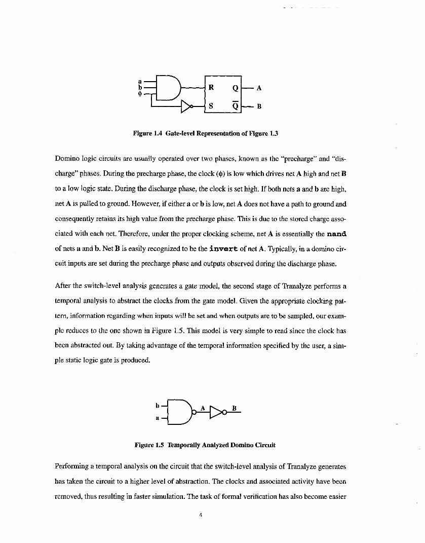
Figure 1.4 Gate-level Representation of Figure 1.3
Domino logic circuits are usually operated over two phases, known as the "precharge" and "dis-
charge" phases. During the precharge phase, the clock (~) is low which drives net A high and net
to a low logic state. During the discharge phase, the clock is set high. If both nets a and b are high,
net A is pulled to ground. However, if either a or b is low, net A does not have a path to ground and
consequently retains its high value from the precharge phase. This is due to the stored charge asso-
ciated with each net. Therefore, under the proper clocking scheme, net A is essentially the rx~tx’xd
of nets a and b. Net B is easily recognized to be the ~.rx~re~’l: of net A. Typically, in a domino cir-
cuit inputs are set during the precharge phase and outputs observed during the discharge phase.
After the switch-level analysis generates a gate model, the second stage of Tranalyze performs a
temporal analysis to abstract the clocks from the gate model. Given the appropriate clocking pat-
tern, information regarding when inputs will be set and when outputs are to be sampled, our exam-
ple reduces to the one shown in Figure 1.5. This model is very simple to read since the clock has
been abstracted out. By taking advantage of the temporal information specified by the user, a sim-
ple static logic gate is produced.
Figure 1.5 Temporally Analyzed Domino Circuit
Performing a temporal analysis on the circuit that the switch-level analysis of Tranalyze generates
has taken the circuit to a higher level of abstraction. The clocks and associated activity have been
removed, thus resulting in faster simulation. The task of formal verification has also become easier
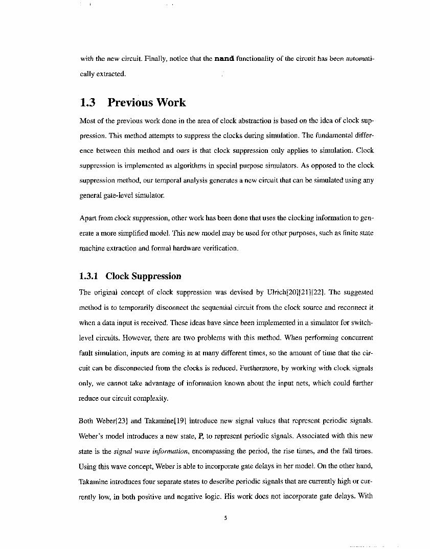
with the new circuit. Finally, notice that the rx~trxd functionality of the circuit has been automati-
cally extracted.
1.3 Previous WorkMost of the previous work done in the area of clock abstraction is based on the idea of clock sup-
pression. This method attempts to suppress the clocks during simulation. The fundamental differ-
ence between this method and ours is that clock suppression only applies to simulation. Clock
suppression is implemented as algorithms in special purpose simulators. As opposed to the clock
suppression method, our temporal analysis generates a new circuit that can be simulated using any
general gate-level simulator.
Apart from clock suppression, other work has been done that uses the clocking information to gen-
erate a more simplified model. This new model may be used for other purposes, such as finite state
machine extraction and formal hardware verification.
1.3.1 Clock Suppression
The original concept of clock suppression was devised by Ulrich[20][21][22]. The suggested
method is to temporarily disconnect the sequential circuit from the clock source and reconnect it
when a data input is received. These ideas have since been implemented in a simulator for switch-
level circuits. However, there are two problems with this method. When performing concurrent
fault simulation, inputs are coming in at many different times, so the amount of time that the cir-
cuit can be disconnected from the clocks is reduced. Furthermore, by working with clock signals
only, wc cannot take advantage of information known about the input nets, which could further
reduce our circuit complexity.
Both Weber[23] and Takamine[19] introduce new signal values that represent periodic signals.
Weber’s model introduces a new state, P, to represent periodic signals. Associated with this new
state is the signal wave information, encompassing the period, the rise times, and the fall times.
Using this wave concept, Weber is able to incorporate gate delays in her model. On the other hand,
Takamine introduces four separate states to describe periodic signals that are currently high or cur-
rently low, in both positive and negative logic. His work does not incorporate gate delays. With
both Weber’s and Takamine’s methods, gains are realized because signals are combined to reduce
the number of periodic signals that need to be evaluated.
Both Weber and Takamine’s models produce good results, with most of the clocking information
being suppressed. However, with either method, there is no guarantee of a full clock suppression,
but rather a "partial clock suppression". Although the number of periodic signals has been
reduced, there may still be some signals that cannot be suppressed by these methods and are thus
evaluated during simulation. Another disadvantage of both Weber and Takamine’s methods is that
with the introduction of new states, new truth tables must be developed for each gate primitive that
incorporates the newly introduced signal values. For Takamine’s method, in which four new states
are introduced, this quickly complicates even the simplest of logic gate truth tables.
A new general approach is called "Static Clock Suppression"[15][ 16]. Razdan performs his analy-
sis on a phase-level model similar to that of COSMOS[7]. A change in any of the clocks is defined
as a new phase. Razdan only allows inputs to change at the beginning of a phase. His algorithm
can be broken down into three parts: Presimulation, Event Analysis, and Augmented Simulation.
During Presimulation, all nets (except constants) are initialized to a logic value X. The clocks are
then assigned their corresponding values for the first phase. An initial event-driven simulation is
performed to determine if the value of the clocks can be propagated to the sequential elements of
the circuit. This is repeatedly done for each phase, and the results are then stored at each net for
each phase. Simplifications are done since only non-X values are stored. During the Event Analy-
sis stage, the nodes are partitioned into modules, which are defined as evaluation functions whose
activity is likely to be suppressed. It is also at this stage that all nodes are scheduled for simulation.
Finally, during the Augmented Simulation stage, an event-driven simulation is performed on all
modules.
Like other work done in this area, this algorithm produces very impressive simulation results with
improvements of up to 200%. However, a few restrictions have been placed with Razdan’s
method. As mentioned earlier, inputs can only be set at phase boundaries. In addition, nets must
stabilize before their values are reported to the user. Thus the user is unable to view nets during an
oscillatory period.

1.3.2 Other methods
Kam [11] generates a finite state machine (FSM) from a transistor netlist, given information relat-
ing to clock signals and clock modules. The method involves performing a fix point computation
of the steady state response. This is similar to symbolically simulating the circuit until it reaches
stability. The FSM generated is described as a binary decision diagram (BDD), as opposed to our
gate-level circuit representation.
One immediate problem with Kam’s method is that it is not able to handle circuits that do not sta-
bilize, i.e. oscillating circuits. Another disadvantage is that inputs can only be changed on phase
boundaries, similar to the restrictions placed by other methods in section 1.3.1.
1.4 Our Approach
All of the previously mentioned methods deal with circuits at a phase-level, meaning data inputs
can only be set at phase boundaries, i.e. when a clock is changed. We remove this limitation by
working with a discrete time model. This allows inputs to be changed and outputs to be sampled at
arbitrary points in time. As opposed to previous approaches, our approach also allows input nets to
take on multiple values in one phase. Similarly, any net can be sampled at multiple points in the
same phase. In effect, these input and output nets are multiplexed into and out of the circuit over a
period of time.
Another limitation of earlier approaches is the lack of a way to deal with oscillating nets. Most of
the previous approaches either could not deal with oscillating nets or merely set the net to be a
logic X. We can display the true value to the user for a given discrete time.
All of the clock suppression approaches are implemented inside a logic simulator. However, we
will generate a new abstracted gate-level circuit that can be simulated using any gate-level simula-
tor. A form of symbolic simulation is used to perform the temporal analysis.
1.5 Organization of the M.S. reportSection 2 will present a detailed description of the temporal analysis that we are performing on cir-
cuits. Section 3 describes the actual implementation of our work, and Section 4 presents our
results. Finally, Section 5 offers concluding remarks.
Section 2
Clock Abstraction
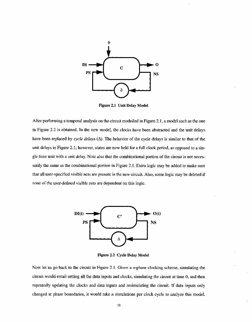
We have developed a tool that abstracts clocks from sequential gate-level circuits. Given a sequen-
tial circuit and the corresponding clocking scheme, we produce a new, simpler circuit that has
implicitly incorporated the clocking scheme. As opposed to traditional phase-level timing
approaches, our approach uses a discrete timing model. After presenting our algorithm, examples
will be given that help to explain our temporal analysis method.
2.1 Discrete Timing Model
2.1.1 Basic Model
It is worthwhile to define the terminology used to describe sequential circuits. Figure 2.1 shows a
basic model for a sequential circuit. Primary inputs (PI), or external inputs, are made up of data
inputs (DI) and clocks (q)). The combinational portion of the circuit (C) uses the primary inputs and
present states (PS) to generate the outputs (O) and next states (NS). The next states are a function
of the inputs and present states, thus implying a Mealy machine model. The states are held during
a zero-delay evaluation of the circuit. The next states are updated to present states as each next
state passes through a unit delay (~). This delay represents the smallest increment of a time delay.
Thus, with a unit delay model a state is held for one time unit.
DI OC
PS NS
Figure 2.1 Unit Delay Model
After performing a temporal analysis on the circuit modelled in Figure 2.1, a model such as the one
in Figure 2.2 is obtained. In the new model, the clocks have been abstracted and the unit delays
have been replaced by cycle delays (A). The behavior of the cycle delays is similar to that of the
unit delays in Figure 2. !; however, states are now held for a full clock period, as opposed to a sin-
gle time unit with a unit delay. Note also that the combinational portion of the circuit is not neces-
sarily the same as the combinational portion in Figure 2.1. Extra logic may be added to make sure
that all user-specified visible nets are present in the new circuit. Also, some logic may be deleted if
none of the user-defined visible nets are dependent on this logic.
DI(t) O(t)C’
PS NS
Figure 2.2 Cycle Delay Model
Now let us go back to the circuit in Figure 2.1. Given a n-phase clocking scheme, simulating the
circuit would entail setting all the data inputs and clocks, simulating the circuit at time 0, and then
repeatedly updating the clocks and data inputs and resimulating the circuit. If data inputs only
changed at phase boundaries, it would take n simulations per clock cycle to analyze this model.
10

However, since we allow data inputs to change outside of phase boundaries, it may actually take
more than n simulations per cycle.
Given the nature of sequential circuits, it is probable that each clock "activates" the circuit during
one phase, and uses the other phases to hold the value. While these other phases do not update the
states, under conventional simulation they still must be simulated. Since there are no clocks in the
circuit in Figure 2.2, this circuit need only be simulated once for each clock cycle.
2.1.2 Timing Specifications
In order to temporally analyze a sequential circuit, the user must provide the temporal details of
the circuit. All primary inputs are set over periods of time, and output nets are sampled at discrete
points in time. This information must be supplied by the user in a separate file.
One restriction of earlier work done in this area was that the inputs can only be changed when
clocks are changed. Our scheme allows the user to change the inputs at any time in a cycle. Thus,
we have chosen to use a discrete timing model over a phase-level timing model. Under a discrete
timing system, data inputs and clocks are set for an interval of time. Clocks must be set to a con-
stant logic value. If the value of a data input is known, it can be set to a logic value. Otherwise, a
symbolic variable is introduced and the data input is set to this variable. Variable names must
explicitly be given by the user for every interval in which an input may take on a different value.
The user must specify the output nets or visible nets in the circuit and the discrete points in time
which the user wishes to sample each output net. Note that whereas data inputs and clocks are
specified over an interval of time, outputs are sampled at discrete points in time. This allows for
nets that oscillate over time to be reported. With traditional simulators such as COSMOS [7], a net
must be stabilized before it can be reported. If the net does not stabilize, i.e. it oscillates, COSMOS
will report an X. With our methodology, we can report unstable values since we are only interested
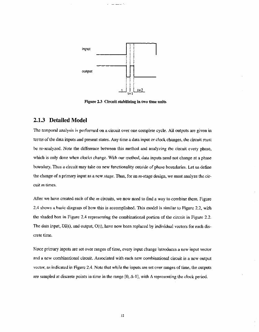
in the value at a particular time. For instance, Figure 2.3 shows a timing diagram for a circuit that
takes two time units to stabilize. With our temporal analysis, the user may sample points at any
discrete time in the cycle, including points t, t+l, and t+2. Traditionally, phase-level simulators will
only report the value after time t+2.
11
input
output
t+2
Figure 2.3 Circuit stabilizing in two time units
2.1.3 Detailed Model
The temporal analysis is performed on a circuit over one complete cycle. All outputs are given in
terms of the data inputs and present states. Any time a data input or clock changes, the circuit must
be re-analyzed. Note the difference between this method and analyzing the circuit every phase,
which is only done when clocks change. With our method, data inputs need not change at a phase
boundary. Thus a circuit may take on new functionality outside of phase boundaries. Let us define
the change of a primary input as a new stage. Thus, for an m-stage design, we must analyze the cir-
cuit m times.
After we have created each of the m circuits, we now need to find a way to combine them. Figure
2.4 shows a basic diagram of how this is accomplished. This model is similar to Figure 2.2, with
the shaded box in Figure 2.4 representing the combinational portion of the circuit in Figure 2.2.
The data input, DI(t), and output, O(t), have now been replaced by individual vectors for each
crete time.
Since primary inputs are set over ranges of time, every input change introduces a new input vector
and a new combinational circuit. Associated with each new combinational circuit is a new output
vector, as indicated in Figure 2.4. Note that while the inputs are set over ranges of time, the outputs
are sampled at discrete points in time in the range [0, A-l], with A representing the clock period.
12
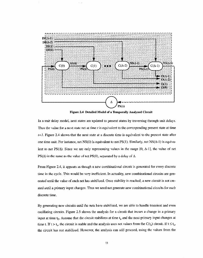
Figure 2.4 Detailed Model of a Temporally Analyzed Circuit
In a unit delay model, next states are updated to present states by traversing through unit delays.
Thus the value for a next state net at time t is equivalent to the corresponding present state at time
t+l. Figure 2.4 shows that the next state at a discrete time is equivalent to the present state after
one time unit. For instance, net NS(0) is equivalent to net PS(1). Similarly, net NS(A-1) is equiva-
lent to net PS(A). Since we are only representing values in the range [0, A-l], the value of net
PS(A) is the same as the value of net PS(0), separated by a delay of
From Figure 2.4, it appears as though a new combinational circuit is generated for every discrete
time in the cycle. This would be very inefficient. In actuality, new combinational circuits are gen-
erated until the value of each net has stabilized. Once stability is reached, a new circuit is not cre-
ated until a primary input changes. Thus we need not generate new combinational circuits for each
discrete time.
By generating new circuits until the nets have stabilized, we are able to handle transient and even
oscillating circuits. Figure 2.5 shows the analysis for a circuit that incurs a change in a primary
input at time t0. Assume that the circuit stabilizes at time t s and the next primary input changes at
time t. If t > ts, the circuit is stable and the analysis uses net values from the C(ts) circuit. If < ts,
the circuit has not stabilized. However, the analysis can still proceed, using the values from the
13
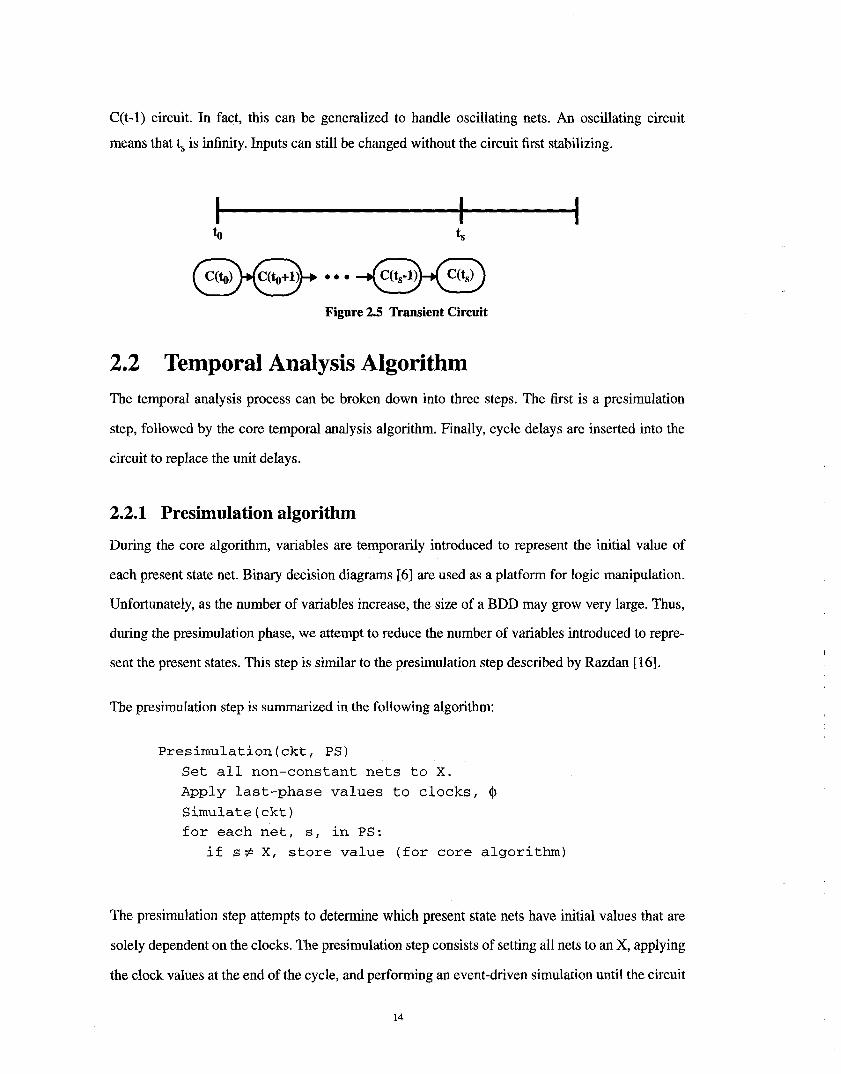
C(t-1) circuit. In fact, this can be generalized to handle oscillating nets. An oscillating circuit
means that t s is infinity. Inputs can still be changed without the circuit first stabilizing.
I I Ito ts
Figure 2.5 Transient Circuit
2.2 Temporal Analysis Algorithm
The temporal analysis process can be broken down into three steps. The first is a presimulation
step, followed by the core temporal analysis algorithm. Finally, cycle delays are inserted into the
circuit to replace the unit delays.
2.2.1 Presimulation algorithm
During the core algorithm, variables are temporarily introduced to represent the initial value of
each present state net. Binary decision diagrams [6] are used as a platform for logic manipulation.
Unfortunately, as the number of variables increase, the size of a BDD may grow very large. Thus,
during the presimulation phase, we attempt to reduce the number of variables introduced to repre-
sent the present states. This step is similar to the presimulation step described by Razdan [16].
The presimulation step is summarized in the following algorithm:
Preslmulation(ckt, PS)
Set all non-constant nets to X.
Apply last-phase values to clocks,
Simulate(ckt)
for each net, s, in PS:
if s~ X, store value (for core algorithm)
The presimulation step attempts to determine which present state nets have initial values that are
solely dependent on the clocks. The presimulation step consists of setting all nets to an X, applying
the clock values at the end of the cycle, and performing an event-driven simulation until the circuit
14
stabilizes. Next, a check is made to see if any of the present state nets have changed from their ini-
tial value of X. If they have, we know that the initial values of these nets are only dependent on the
clocks. Thus, we need not introduce new variables for these present states. Instead, the constant
values of these nets are stored for the core algorithm. In the core algorithm, we simply initialize
these present state variables to the constants generated during the presimulation stage.
2.2.2 Core Temporal Analysis algorithm
Once a presimulation of the circuit has been performed and all of the data input and present state
variables have been introduced, the main procedure is invoked. An algorithm for the analysis is
presented below. The routine S~dzol±cS±mulate performs a zero-delay symbolic simulation
of the circuit. More about the symbolic simulator will be covered in the next section. This routine
takes in a circuit called cke and generates a new temporally analyzed circuit called ckt’, while
leaving ckt unchanged.
Clock_cycle(ckt)
time : 0
apply inputs and clocks at time O.
apply constant present states (from Presimulation)
introduce variables for non-constant present states
SymbolicSimulate(ckt)
for each unique net in ckt, create new net in ckt’
sample outputs at time 0
while (time < cycle_time):
apply any new data inputs and/or clocks
SymbolicSimulate(ckt)
for each net in ckt
if there is no logically equivalent net in ckt’,
create new net
sample outputs at current time
update time to point of next change in data input or
clock
return ckt’
The procedure analyzes the circuit for one complete clock cycle. It begins by applying values to
constant data inputs and clocks at time 0. Non-constant data inputs and present state nets are
assigned symbolic variables. Then a zero-delay symbolic simulation of the circuit is performed
15
until the circuit stabilizes. After each symbolic simulation call, nets are added to ckt’. Logical
equivalence is checked by building up BDDs for each net.
2.2.3 Cycle delays
In the core algorithm, present states for the first stage were represented by introducing new vari-
ables. These were created for temporary purposes, as they actually represented states from the pre-
vious cycle. Upon completion of the core temporal analysis algorithm, these variables must be
removed. The initial present state nets become cycle delays to the next state nets in the last stage.
Referring back to Figure 2.4, the initial present state nets are PS(0). The next state nets in the last
stage are NS(A-1). Note that this net is equivalent to the value of the artificial net PS(A). After
present and next state nets have been created, the temporary variables introduced for the PS(0) nets
are replaced by cycle delays to PS(A) nets.
Since the cycle delays are dependent on the values of the next states in the last stage, we must
ensure that each of these nets are represented in our circuit. Thus, the temporal analyzer automati-
cally identifies each of the state nets and marks each of these nets to be visible at time ’cycle_time
- 1’, which is the last discrete time in our cycle. The values at this time represent the values in the
last stage of the cycle, and thus guarantees that the next states in the last stage will be represented
in the temporally analyzed circuit.
2.3 Examples
We now introduce two examples to illustrate the points made previously. The first is a simple static
Delay flip-flop. The second is bit more complicated as it incorporates a pipelined architecture and
multiplexed pins.
2.3.1 Delay Flip-flop
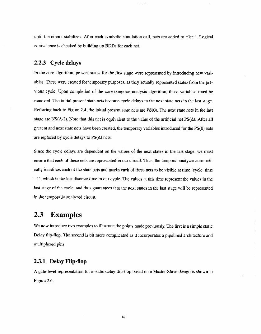
A gate-level representation for a static delay flip-flop based on a Master-Slave design is shown in
Figure 2.6.
16
d
A
B
Figure 2.6 Gate.level Delay Flip-flop
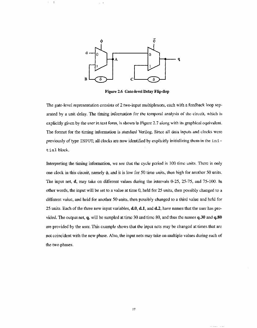
The gate-level representation consists of 2 two-input multiplexors, each with a feedback loop sep-
arated by a unit delay. The timing information for the temporal analysis of the circuit, which is
explicitly given by the user in text form, is shown in Figure 2.7 along with its graphical equivalent.
The format for the timing information is standard Verilog. Since all data inputs and clocks were
previously of type IlqPUT, all clocks are now identified by explicitly initializing them in the ±n± -
t±a]_ block.
Interpreting the timing information, we see that the cycle period is 100 time units. There is only
one clock in this circuit, namely ~), and it is low for 50 time units, then high for another 50 units.
The input net, d, may take on different values during the intervals 0-25, 25-75, and 75-100. In
other words, the input will be set to a value at time 0, held for 25 units, then possibly changed to a
different value, and held for another 50 units, then possibly changed to a third value and held for
25 units. Each of the three new input variables, d.0, d.1, and d.2, have names that the user has pro-
vided. The output net, q, will be sampled at time 30 and time 80, and thus the names q.30 and q.80
are provided by the user. This example shows that the input nets may be changed at times that are
not coincident with the new phase. Also, the input nets may take on multiple values during each of
the two phases.
17
reg d.O,
initial
begin
phi =
end
d.l, d.2, q.30, q.80;
/* all new variables declared */
l’bO; /*phi initialized to a 0 and identified to
be a clock */
always
begin
d =
#25
#5
#20
#25
#5
#20
end
d. 0 ; /* input format: old net = new net "/
d = d. 1 ; /*advance 25 time units and then set input */
q. 3 0 = q; /* output format: new net = oM net */
phi = l’bl;
d = d.2;
q. 80 = q;
phi = i’ bO ; ~*full cycle */
0 50 100
q ~ -~q.30 q.80
Figure 2.7 Timing Information for Delay Flip-flop
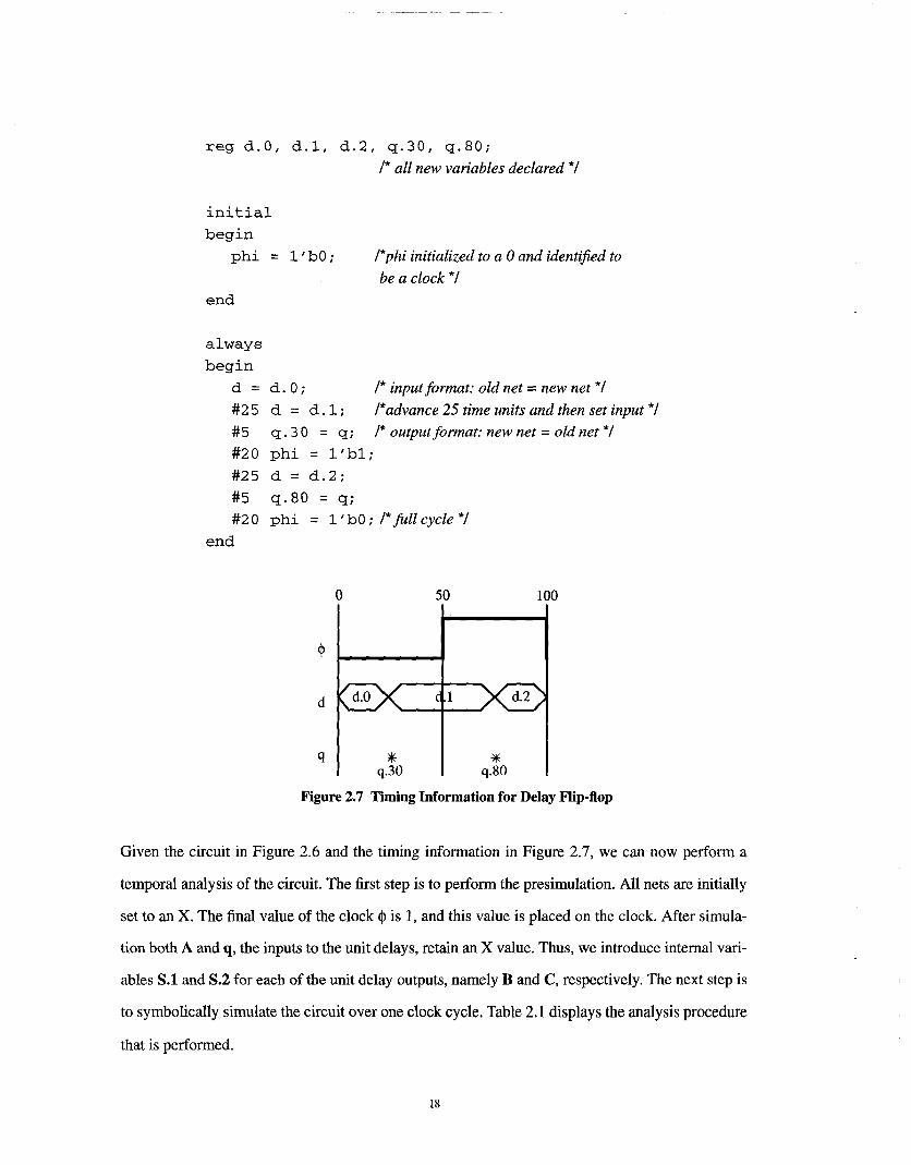
Given the circuit in Figure 2.6 and the timing information in Figure 2.7, we can now perform a
temporal analysis of the circuit. The first step is to perform the presimulation. All nets are initially
set to an X. The final value of the clock ~ is 1, and this value is placed on the clock. After simula-
tion both A and q, the inputs to the unit delays, retain an X value. Thus, we introduce internal vari-
ables S.1 and S.2 for each of the unit delay outputs, namely B and C, respectively. The next step is
to symbolically simulate the circuit over one clock cycle. Table 2.1 displays the analysis procedure
that is performed.
18
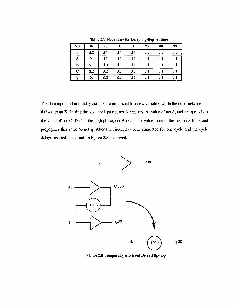
Table 2.1 Net values for Delay flip-flop vs. time
Net 0- 25 30 50 75 80 99
d d.0 d.1 d.1 d.1 d.2 d.2 d.2
A X d.1 d.1 d.1 d.1 d.1 d.1
B S.1 d.0 d.1 d.1 d.1 d.1 d.1
C S.2 S.2 S.2 S.2 d.1 d.1 d.1
q X S.2 S.2 d.1 d.1 d.1 d.1
The data input and unit delay outputs are initialized to a new variable, while the other nets are ini-
tialized to an X. During the low clock phase, net A receives the value of net d, and net q receives
the value of net C. During the high phase, net A retains its value through the feedback loop, and
propagates this value to net q. After the circuit has been simulated for one cycle and the cycle
delays inserted, the circuit in Figure 2.8 is derived.
d.1~ q.80
d.1 C.100
C.0 q.30
0,1 m
Figure 2.8 Temporally Analyzed Delay Flip-flop
q.30
19

Interpreting these results, we see that q.$0 is simply an ident to the data input d.1, set during the
middle 50 time units. From the figure, it appears as though the input net is transparently passed to
the output net, which seems to conflict with the definition of an edge-triggered flip-flop. But let us
be careful in interpreting these results. From Figure 2.7, we see that net d.1 is set during the time
interval 25-75, while the output q.80 is viewed at time 80 units. The input gets latched at the posi-
tive edge of the clock (time 50) and thus the value of the input is only important at this point. Thus
the ident gate shows that the output is identically equal to the input only under the timing con-
ditions specified by the user.
Output net q.30 is now a 100-unit (cycle-time) delay to the input d.1. At time 30, net q was deter-
mined to be equivalent to the initial value at net C. The value of net q at time 99, which is equiva-
lent to the value of net C at time 100, is d.1. Thus the temporary variable S.2 is replaced by a cycle
delay to d.1. This implies that the value of net q at time 30 is equivalent to value of d.1 set in the
previous cycle. Remembering the operation of a delay flip-flop, we see that this is what we would
expect. At times other than the positive clock edge, the output of the flip-flop holds the value of the
input set during the most recent positive clock edge. The temporal analysis thus inserts a cycle-
level delay to represent the value from the previous cycle.
Finally, note that the output nets are only a function of d.1. The user-specified output nets do not
depend on the values of d.0 or d.2. Once again, this is what we would expect: only the value of the
data input during the positive clock edge is important. This is a useful "side-effect" of the temporal
analysis: we can now determine when the value of the inputs are relevant to the operation of the
circuit.
The temporal analysis only required the user to specify the clocking pattem and information
regarding when inputs will be set and outputs observed. Unlike other possible approaches, none of
the following were required: explicit identification of state elements; timings of internal state sig-
nals; or a high level description of the desired functionality.
20
2.3.2 Mead and Conway Stack
The temporal analysis can also correctly evaluate pipelined circuits and multiplexed pins. Figure
2.9 shows a block diagram for a stack, as described by Mead and Conway [13].
Iin S0 S1 Sna
So
:
Si-1
SiSi+l:
Sn-1
Figure 2.9 Block Diagram for Mead and Conway Stack
A PUSH operation will shift the data input (in) into the stack and shift stored data (Si) deeper into
the stack. A POP operation does the reverse -- the data stored in state SO is outputted and the rest of
the data is shifted up one level. The third mode is a HOLD, which retains the states in the stack.
The circuit uses a two-phase nonoverlapping clock. The mode of operation is selected by the
sequence of values on the op signal. Figure 2.10 shows the timing for the circuit.
21
50
t-1
100 150I
2OO 250
t
300 350
I400
op
in
state
out
aim ~x
Our’Cycle~5 1~5 175 200
(opzt.13
~" OUt. "h
Figure 2.10 Timing Diagram for Stack
To represent the three modes, two states are multiplexed onto the control signal op. Note that op2
is set during the previous cycle, therefore creating a pipelined design. The following table gives
the encoding for the modes of operation.
op2
2.2 Modes of Operation for Stack
stackopl mode operation
1 0 PUSH Si_1 -->Si0 1 POP Si+1 --->Si0 0 HOLD Si--)Si
In order to incorporate all of the input information in one clock cycle, we have chosen to shift the
cycle boundaries, as shown in Figure 2.10. As the user, we have chosen output net out to be visible
22
at time 50 within our cycle. This net is a function of the data input from the previous cycle and the
op-signal from both the previous and present cycles.
Figure 2.11 shows a generalized section of the circuit generated after the temporal analysis has
been performed. The shaded region in the figure represents the circuitry required for the i th bit of
the stack. Since all three inputs to MuxC are delayed, we can replace these three input delays with
a single delay at the output of Si. The shaded circuit can then be reduced to a four-input mux as
shown in the figure. Referring back to Table 2.2, the functionality of state Si is correct for the three
modes of operation. For example, when opl=op2=0, a HOLD operation is performed. From Fig-
ure 2.11, this means that states Si+l, Si, and Si. 1 all retain their previous value. For a POP opera-
tion, the values of the states get updated as follows: Si+2-~Si+l, Si+l---)Si, and Si----~Si. 1. The values
in each state is shifted up one level. The operation of the PUSH is similar. The fourth case, when
both opl and op2 are high, was designed to be a don’t care. Our temporal analyzer has correctly
identified this case to implement a HOLD operation.
23
(POP)
Si+l
op2
op2
opl
Dopl
Si+l
(HOLD) Siop2
Si
(PUSH)
Si.1
Si.2
op2
Dopl
Si.1
HOLD
POP
PUSH
HOLD
Si
Si
Si
Figure 2.11 Temporally analyzed stack (generalized)
Note that MuxA is shared between circuitry for the i th bit and the i÷l th bit. Similarly, MuxB is
shared between circuitry for the i th bit and the i-1th bit. In fact, an n-bit stack can be represented in
3n+C gates, where C represents the constant circuitry required to set up the stack. The thick line
represents the added circuitry with each bit.
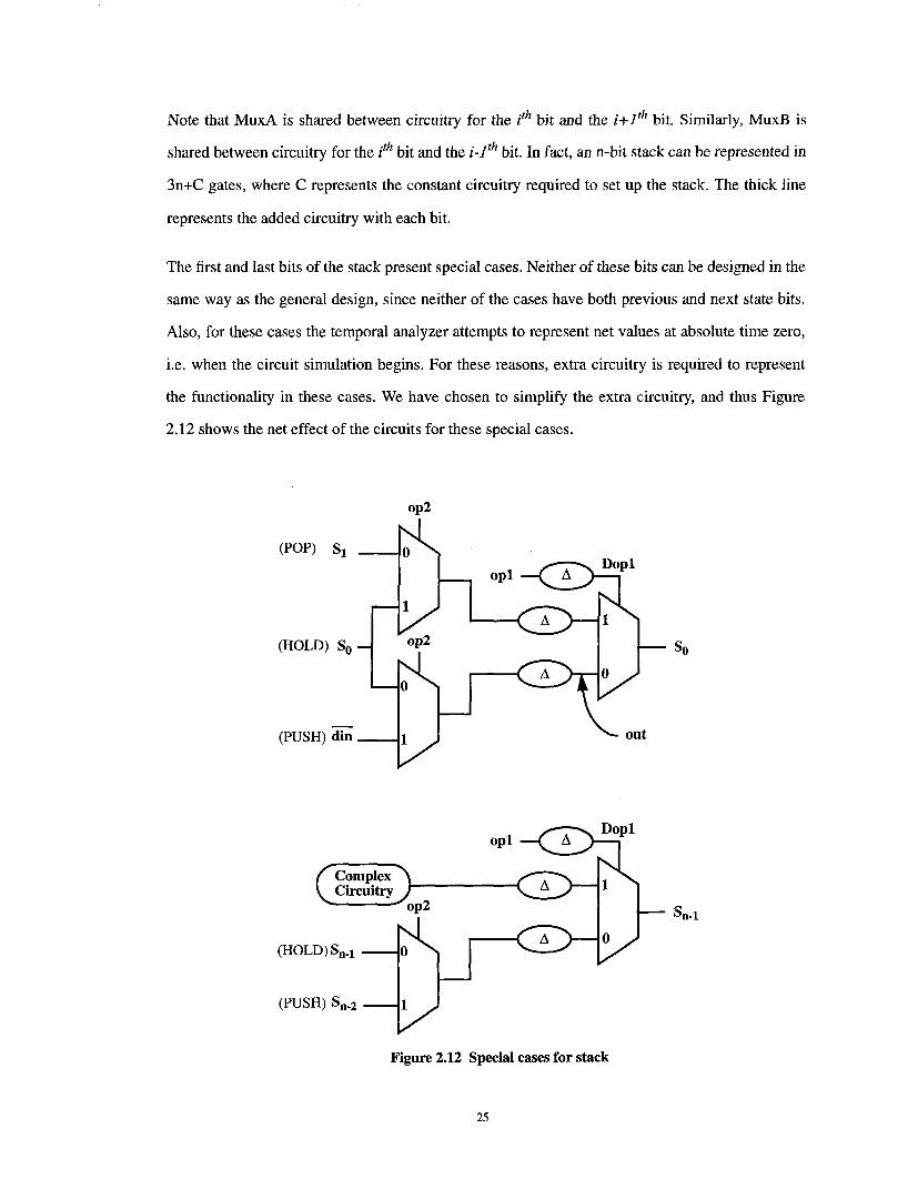
The first and last bits of the stack present special cases. Neither of these bits can be designed in the
same way as the general design, since neither of the cases have both previous and next state bits.
Also, for these cases the temporal analyzer attempts to represent net values at absolute time zero,
i.e. when the circuit simulation begins. For these reasons, extra circuitry is required to represent
the functionality in these cases. We have chosen to simplify the extra circuitry, and thus Figure
2.12 shows the net effect of the circuits for these special cases.
(POP)
(HOLD)
(PUSH) din
op2
1
SOop2
Complex TM
Circuitry_/
(HOLD) Sn. 1 ~ ~
(PUSH) Sn. 2 ~
Figure 2.12 Special cases for stack
25
The first bit circuitry is similar to the generalized case, with din replacing what would be the S.1
net. Notice that the output net out is independent of the value on opl. The op2=l case corresponds
to the PUSlt or a I-IOLD case, and the output is equivalent to din. The op2=0 case corresponds to
the POP or a HOLD case, and the output is equivalent to S0. The output is only interesting during
the POP operation, and here it correctly produces the storage net So.
With the last bit circuitry, a POP operation cannot be performed, since we are at the maximum
depth of the stack. Due to charge sharing, complex circuitry is generated for the case when Dopl =
1, and thus the value is undetermined here. Thus, for the last bit the (opl=op2=0) I/OLD operation
and PUSI/operation are valid, but the (opl=op2=l) t/OLD and POP operations are not. However,
we are not concerned with the last two op-patterns for the last bit. The I/OLD operation is only
defined when opl=op2=0. The POP operation is invalid at the bottom of the stack.
26

Section 3
Implementation
We have chosen to incorporate our temporal analysis within Tranalyze, the tool that extracts gate-
level representations from a transistor-level circuit. This section describes the details of Tranalyze
and the symbolic simulator used in our temporal analysis.
3.1 Tranalyze
Tranalyze [9] takes a switch-level circuit and generates a functionally equivalent gate-level circuit.
Tranalyze is able to capture aspects of switch-level circuits such as hi-directional transistors, pre-
charged logic, stored charge, and multiple signal strengths.
3.1.1 Logic States
Tranalyze uses a 4-valued set of logic states, namely {Z, 0, 1, X}. The Z value indicates a "high-
impedance" value such as those found in tri-state buffers. The X value indicates either an unknown
or indeterminate value. An unknown value is one which is either logic 0 or 1 but is not known,
whereas an indeterminate value represents a non-digital voltage due to the shorting of the ground
and power rails or the decay of stored charge. A partial ordering [10] has been imposed on the set
of logic states under the relation <, as shown in Figure 3.1. The partial ordering implies that a func-
tion defined under this set of logic states is monotonic. Thus if f(X) = c, where c is a value in the
subset {Z, 0, 1 }, then it must be true that f(Z) = f(0) = f(1)
27
0 1 Z
X
Figure 3.1 Partial Ordering of Logic Values
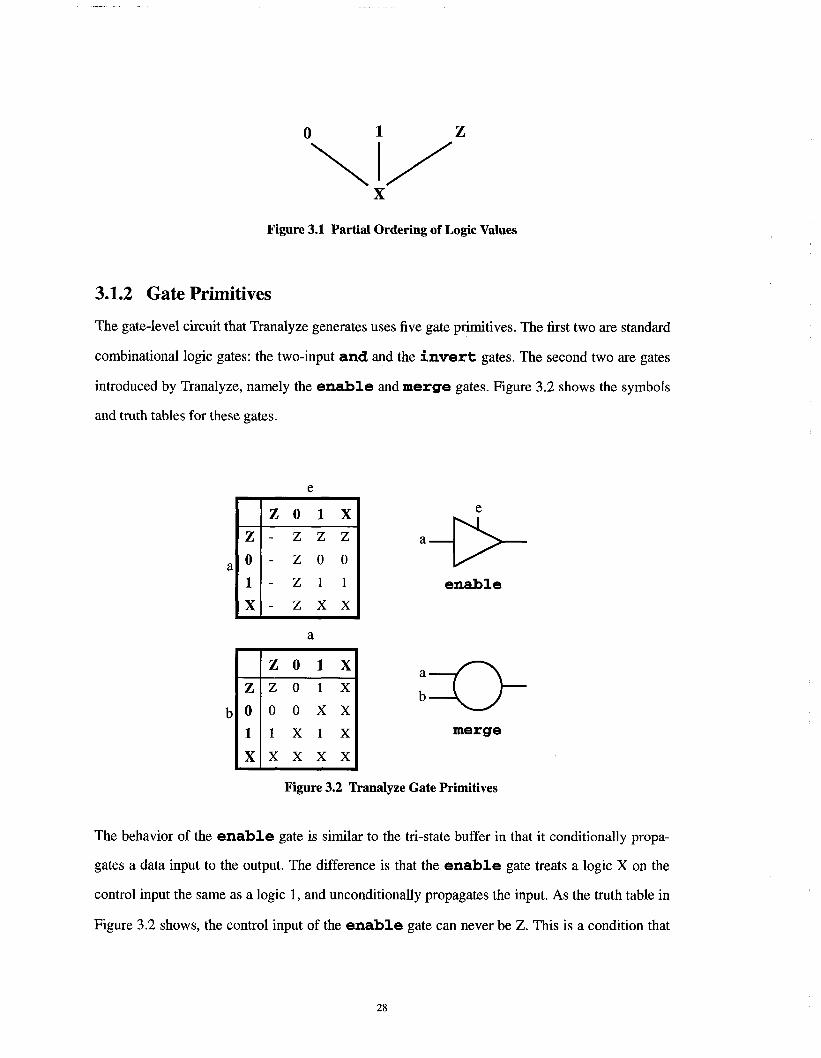
3.1.2 Gate Primitives
The gate-level circuit that Tranalyze generates uses five gate primitives. The first two are standard
combinational logic gates: the two-input and and the in~rert gates. The second two are gates
introduced by Tranalyze, namely the enable and m@rge gates. Figure 3.2 shows the symbols
and truth tables for these gates.
a
b
e
Z 0 1 X
Z Z Z Z
0 Z 0 01 Z 1 1X Z X X
a
e
enable
Z 0 1 X
Z Z 0 1 X
0 0 0 X X1 1 X 1 XX X X X X
merge
Figure 3.2 Tranalyze Gate Primitives
The behavior of the enable gate is similar to the tri-state buffer in that it conditionally propa-
gates a data input to the output. The difference is that the enable gate treats a logic X on the
control input the same as a logic 1, and unconditionally propagates the input. As the truth table in
Figure 3.2 shows, the control input of the enable gate can never be Z. This is a condition that
28
Tranalyze will ensure. The merge gate can be thought of as a "wired-logic" function as it combines
two nets. Each net in Tranalyze can be driven by only one gate, thus the reason for a mer~e gate.
The last gate is a delay gate, which inserts a unit-delay into the circuit. All other gates are zero-
delay.
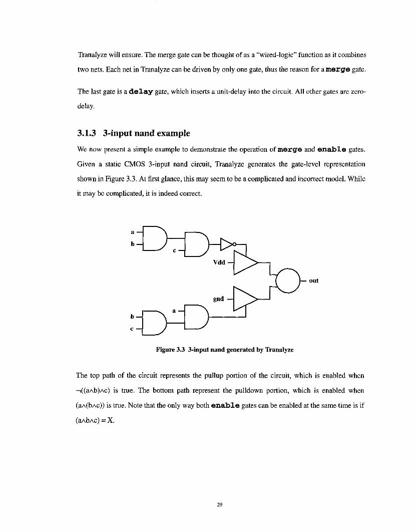
3.1.3 3-input nand example
We now present a simple example to demonstrate the operation of mettle and enable gates.
Given a static CMOS 3-input nand circuit, Tranalyze generates the gate-level representation
shown in Figure 3.3. At first glance, this may seem to be a complicated and incorrect model. While
it may be complicated, it is indeed correct.
out
gnd --] ~
Figure 3.3 3-input nand generated by Tranalyze
The top path of the circuit represents the pullup portion of the circuit, which is enabled when
~((a^b)^c) is true. The bottom path represent the pulldown portion, which is enabled
(a~(bAc)) is true. Note that the only way both enable gates can be enabled at the same time is
(a~b^c) =
29
3.1.4 Redundancy check
As mentioned earlier, our temPoral analysis builds a new circuit by making multiple copies of the
original circuit, inserting only non-redundant nets into the new circuit. Since redundancy detection
is such an important part of the analysis, this procedure is described in greater detail.
Referring again to the circuit in Figure 3.3, we see a limitation of the switch-level analysis in Tran-
alyze. It is unable to exploit the associative property of the a.nd operation and thus inserts redun-
dant logic. A version of Tranalyze was implemented by building up BDDs while analyzing the
switch-level circuit [3]. BDDs offer a canonical representation for logic functions and thus testing
for equivalence is a constant-time operation. While this eliminated the redundancies generated by
Tranalyze, the cost of using BDDs in the analysis process was very high. Upon experimentation, it
was discovered that a cheaper method could be implemented that uses BDDs to test for redun-
dancy after a gate-level model has been generated [5]. BDDs are built up for each net, starting
from the primary inputs and present states, and working outwards to the outputs and next states. As
each BDD is constructed, it is tested to see if an equivalent net already exists in the circuit. If it is
found to be equivalent to another net, the net with the greater fanin circuitry is removed, provided
it is not being used for anything else. If at any time the memory used by BDDs becomes too large,
the redundancy detection is halted. However, since redundancies are recognized and removed
while the BDDs are being constructed, some reduction is still accomplished. While this postpro-
cessing method of redundancy checking may not remove all of the redundancies in a circuit, it has
been very effective in finding and removing redundancies at a fraction of the cost of the original
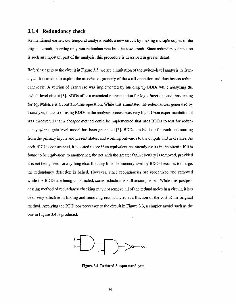
method. Applying the BDD postprocessor to the circuit in Figure 3.3, a simpler model such as the
one in Figure 3.4 is produced.
out
Figure 3.4 Reduced 3-input nand gate
30
Since the size of a BDD is very dependent upon the variable ordering, heuristics are used to pro-
duce a "good" ordering. During the redundancy analysis, which is performed after the circuit has
been constructed, we use heuristics [3] to assign a variable ordering. The heuristic first assigns a
height to each net. Assume a net p with inputs {il...in}. Let hp denote the height of net p. Then
t O, pe PIhp = MAX (hi1 .... hi. ) + 1, otherwise
(EQ 1)
The heuristic algorithm is as follows:
Sort all ~true" outputs (no fanout) by decreasing heightFor each output net
Traverse back on input with greatest heightIn case of a tie, choose input with greatest fanout count
Create new variable at input or present state net
This algorithm rearranges the circuit so that as inputs and present states are encountered, variables
are created as per the heuristic. The heuristic tries to find the longest path from an output to an
input and creates a variable for this input. This process is repeated until all variables have been cre-
ated. While the variable ordering may not be optimal, the heuristic ensures a "good" ordering for
most circuits.
3.1.5 Unit delays
Before analyzing the switch-level circuit, Tranalyze checks to see if there are any zero-delay
cycles. If one is found, a unit-delay is inserted into the circuit to break the cycle. Tranalyze then
ensures that each gate-level circuit that it generates will not have any zero-delay cycles in the cir-
cuit. The circuit that Tranalyze generates can be modeled exactly like the one in Figure 2.2. Under
this model, present state variables (S) are easily identified as the output of unit delays. Therefore,
this model lends itself well for performing temporal analysis.
In order to perform a temporal analysis on the circuit, all of the data inputs and present states must
be identified. Identifying the data inputs is generally very straight-forward. Identifying all of the
31

present states in the circuit, generally thought of as the output of unit delays, requires more effort.
Tranalyze builds a directed acyclic graph (DAG) of the circuit with each node representing a net
the circuit and each edge a gate. Figure 3.5 shows the DAG for the circuit in Figure 2.6.
Figure 3.5 DAG for Delay Flip-Flop in Figure 2.6
Feedback loops present a problem because they become cycles when a DAG is constructed, as
shown by the faded line in Figure 3.5. We can eliminate these cycles by breaking the cycles at the
unit delays. Thus, if we make inputs and unit delays the leafs of the DAG, we can generate a DAG
for sequential circuits with feedback loops.
3.1.6 Domino Example
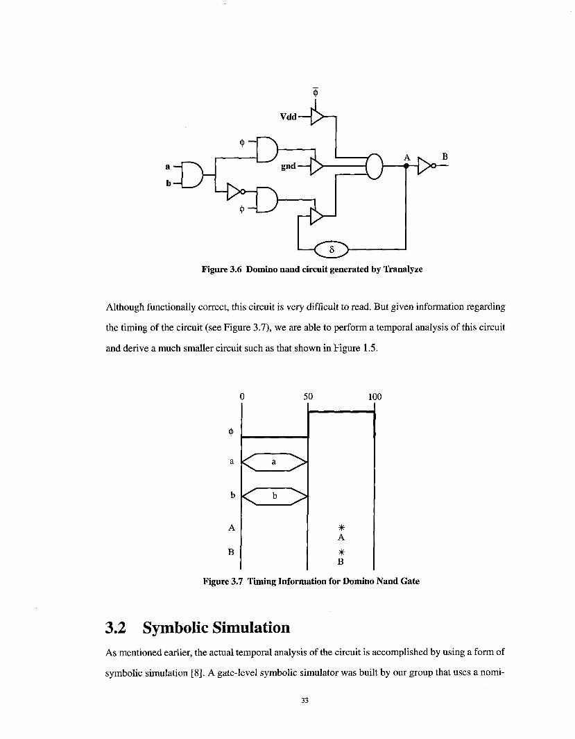
In section 1.2, we described a domino nand circuit. The gate-level circuit generated by Tranalyze
is very complicated as shown in Figure 3.6. For sake of simplicity, we have replaced a pair of
sequential merge gates generated by Tranalyze by one three-input merge gate.
Node A effectively represents the nand of inputs a and b, and node B is the and of the two. Ana-
lyzing this circuit, we see that if the clock ~ is low only the top enable gate is on and Vdd
passes through to A. If the clock and the data inputs a and b are all high, ground is passed through
to A. Finally, the default case is that the value of A is simply the previous value of A, delayed by
one time unit. This feedback is attributed to the stored charge implicit on every node.
32
Vdd---~
Figure 3.6 Domino nand circuit generated by Tranalyze
Although functionally correct, this circuit is very difficult to read. But given information regarding
the timing of the circuit (see Figure 3.7), we are able to perform a temporal analysis of this circuit
and derive a much smaller circuit such as that shown in Figure 1.5.
0 50 100
a
A
B
A
B
Figure 3.7 Timing Information for Domino Nand Gate
3.2 Symbolic Simulation
As mentioned earlier, the actual temporal analysis of the circuit is accomplished by using a form of
symbolic simulation [8]. A gate-level symbolic simulator was built by our group that uses a nomi-
33
nal, transport delay model. In this section, we will discuss different delay models, different types
of simulation, and bring up issues regarding binary decision diagrams.
3.2.1 Delay models
When doing gate-level simulation, there are two models commonly used to represent delays[l].
The first is a transport delay model, and the second is an inertial delay model. A transport delay
model unconditionally propagates input and gate delays to the output. An inertial delay model is
derived from the fact that all circuits require energy to switch. If the input pulse given to the circuit
is too short, the output signal may suppress or filter the signal. Unlike transport delay models, an
inertial delay output may not propagate all the values of its inputs. We use a transport delay model
in our symbolic simulator. In fact, most conventional symbolic simulators use a transport delay
model. However, Seger and Bryant [18] have shown how an inertial delay model can be used with
symbolic simulation.
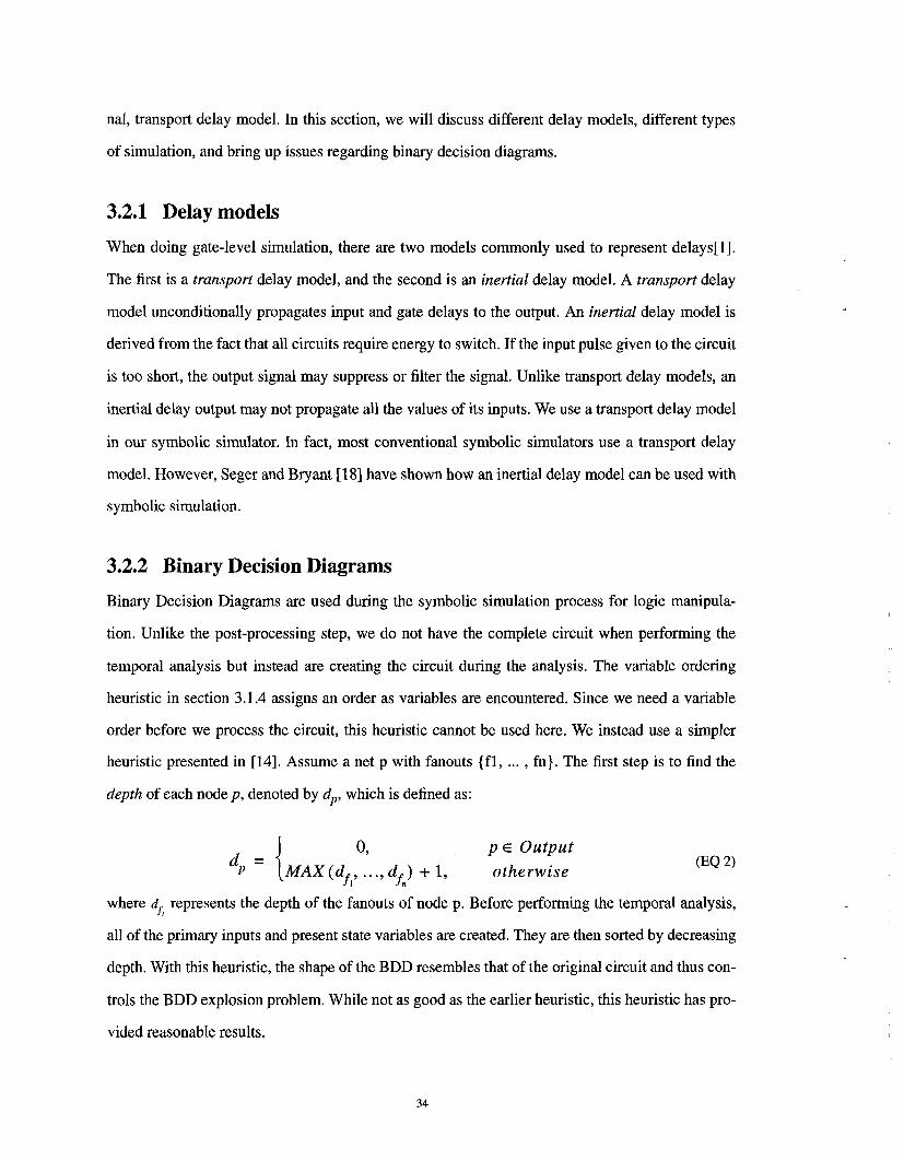
3.2.2 Binary Decision Diagrams
Binary Decision Diagrams are used during the symbolic simulation process for logic manipula-
tion. Unlike the post-processing step, we do not have the complete circuit when performing the
temporal analysis but instead are creating the circuit during the analysis. The variable ordering
heuristic in section 3.1.4 assigns an order as variables are encountered. Since we need a variable
order before we process the circuit, this heuristic cannot be used here. We instead use a simpler
heuristic presented in [14]. Assume a net p with fanouts {fl, ..., fn}. The first step is to find the
depth of each node p, denoted by dp, which is defined as."
t O, p ~ Output(EQ2)
MaX(df~,...,df) + 1, otherwise
where dy, represents the depth of the fanouts of node p. Before performing the temporal analysis,
all of the primary inputs and present state variables are created. They are then sorted by decreasing
depth. With this heuristic, the shape of the BDD resembles that of the original circuit and thus con-
trois the BDD explosion problem. While not as good as the earlier heuristic, this heuristic has pro-
vided reasonable results.
34
3.2.3 Types of Simulation
Simulators are classified along two orthogonal dimensions [2], which will now be discussed. Sim-
ulation algorithms are classified as event-driven and oblivious. The control scheme deals with the
type of implementation used and can be compiled or interpretive.
With an oblivious or levelized simulation algorithm, each gate is evaluated exactly once for each
time point. Thus, the number of evaluations is a fixed number for a particular network. With an
event-driven simulation algorithm, a gate is evaluated if any of its inputs have changed. Typically,
this is a more efficient method than oblivious. However, depending on the gate evaluation
sequence, some gates may be computed multiple times at one time point. Given a circuit that has a
large amount of external changes, an event-driven simulation algorithm may actually prove to be
less efficient than an oblivious algorithm.
The two common types of implementation methods are interpretive and compiled. Interpretive
uses a data structure that represents the network. This model is straight forward, since it follows
the method done when simulating a network by hand. However, this method is inefficient since the
cost of traversing through the data structures is high. A compiled simulator produces an executable
program that efficiently simulates the network. It may even use assembly code to achieve maxi-
mum efficiency.
Most simulators choose to use a compiled simulator with an oblivious algorithm or an interpretive
simulator with an event-driven algorithm. The reason for this is explained by Lewis [12], and will
not be discussed here. One notable exception is COSMOS [7], which uses a compiled simulator
with an event-driven algorithm.
We have chosen to use an interpretive simulator for our temporal analysis, since the data structures
for the network is already set up by Tranalyze. We initially chose to implement the simulator with
a classic event-driven method. However, since many gates were evaluated more than once, an
event-driven simulator became very inefficient. Furthermore, given the nature of sequential cir-
cuits, a casual observation is that clocks have high fanouts. Thus, a change in a clock results in sig-
nificant amounts of activity to the circuit. The method implemented is as follows: when a clock
changes, a levelized simulation is performed. If the scheduled simulation is not due to a clock
35
change, i.e. a data input change or a state variable being updated, an event-driven simulation is
performed.
While this mixed method produced better results than using just one of the simulators, other meth-
ods were looked into that would make the simulation more efficient. One possible method is to use
a "modified event-driven" simulator, which enqueues nets in sorted order, thus eliminating the
possibility of evaluating a gate multiple times during simulation to find a steady state value. The
advantage is that one simulator could be used for all cases, as opposed to the current setup. How-
ever, this method may require a large overhead.
An improvement was later made to the levelized simulator used in the temporal analysis. In this
"modified levelized" simulator, each node is given an evaluation flag. Before each simulation, all
flags are reset. Any primary input that is changed causes that net to have its evaluation flag set.
Before simulating a gate, the evaluation flags of the inputs of the gate are checked and a simulation
is performed if and only if the flag of one of its inputs is set. Upon evaluation of a gate, the flag on
the output net of the gate is set. Thus, we will only evaluate a gate if at least one of its inputs have
changed.
This modified levelized / event-driven simulation method may seem more costly than the modified
event-driven simulation method, since every net’s flag must be reset before each simulation. How-
ever, unlike a classic simulator, the evaluation of a gate is very costly and efforts should be focused
on reducing the number of gate evaluations. The reason for the high cost is that the symbolic eval-
uations are done by building up BDDs for each net, and performing a series of BDD operations
that correspond to the gate primitives. Unfortunately, BDD sizes can grow very large, thus slowing
down the simulator. Thus, the efficiency of our modified levelized / event-driven simulator should
compare with the modified event-driven simulator.
36
Section 4
Results
Tranalyze was originally developed as a replacement to COSMOS [7], a pre-existing switch-level
simulator. We will compare the performance of Tranalyze versus COSMOS in the first section.
Then we will show the improvement and added cost of using BDDs to detect redundant nets.
Finally, we shall show the results obtained by the temporal analysis performed on the gate-level
circuits generated by Tranalyze.
4.1 Tranalyze vs. COSMOSCOSMOS was developed to simulate switch-level circuits. Internal to COSMOS is a tool called
ANAMOS that performs a switch-level analysis of a circuit. After ANAMOS analyzes the circuit,
COSMOS performs a compiled-code event-driven simulation.
Tranalyze, on the other hand, extracts from a switch-level circuit a functionally equivalent gate-
level representation that can be simulated using any conventional hardware simulator. We have
simulated our tests using Cadence Verilog-XL 1.7. Table 4.1 and Table 4.2 show a comparison
between COSMOS and Tranalyze. The first table shows the gate count of Tranalyze vs. COSMOS,
and the second table compares the analysis, compilation, and simulation times of the two. All test
results presented in this section were performed on a DEC 5000 workstation with 50 MB of RAM.
37
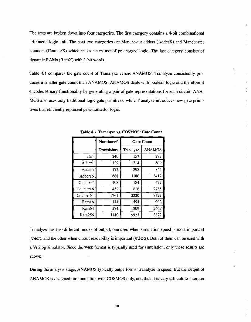
The tests are broken down into four categories. The first category contains a 4-bit combinational
arithmetic logic unit. The next two categories are Manchester adders (AdderX) and Manchester
counters (CounterX) which make heavy use of precharged logic. The last category consists
dynamic RAMs (RamX) with 1-bit words.
Table 4.1 compares the gate count of Tranalyze versus ANAMOS. Tranalyze consistently pro-
duces a smaller gate count than ANAMOS. ANAMOS deals with boolean logic and therefore it
encodes ternary functionality by generating a pair of gate representations for each circuit. ANA-
MOS also uses only traditional logic gate primitives, while Tranalyze introduces new gate primi-
tives that efficiently represent pass-transistor logic.
Table 4.1 Tranalyze vs. COSMOS: Gate Count
Number of
Transistors
Gate Count
Tranalyze ANAMOS
alu4 240 157 277
Adderl 129 214 609
Adder4 172 298 844
Adderl6 688 1186 3412
Counter4 108 184 677
Counter 16 432 816 2765
Counter64 1761 3320 8333
Raml6 144 594 902
Ram64 374 1809 2667
Ram256 1140 9927 8372
Tranalyze has two different modes of output, one used when simulation speed is most important
(~re~’), and the other when circuit readability is important (arlog). Both of them can be used
a Verilog simulator. Since the ~re~" format is typically used for simulation, only these results are
shown.
During the analysis stage, ANAMOS typically outperforms Tranalyze in speed. But the output of
ANAMOS is designed for simulation with COSMOS only, and thus it is very difficult to interpret
38
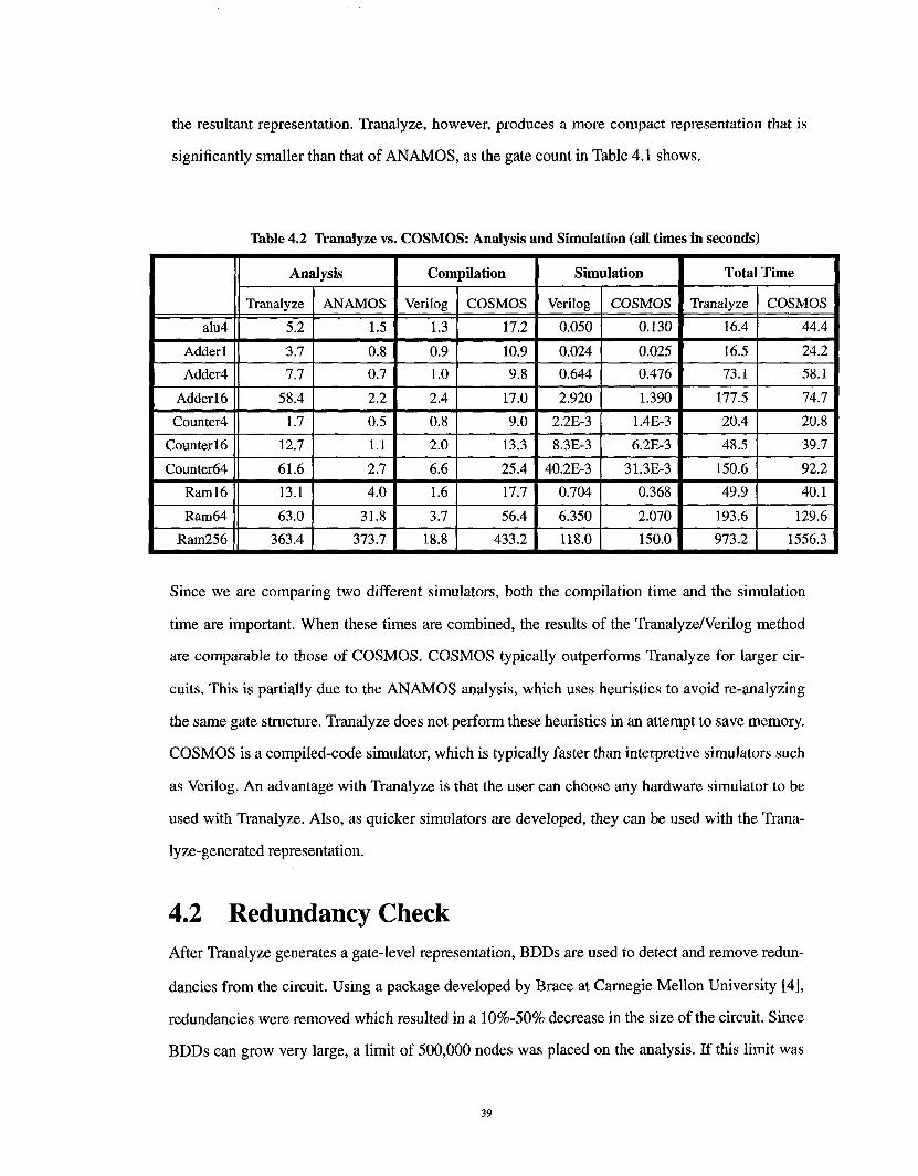
the resultant representation. Tranalyze, however, produces a more compact representation that is
significantly smaller than that of ANAMOS, as the gate count in Table 4.1 shows.
alu4
Adderl
Adder4
Adderl6
Counter4
Counter 16
Counter64
Raml6
Table 4.2 Tranalyze vs. COSMOS: Analysis and Simulation (all times in seconds)
Analysis
Tranalyze
5.2
3.7
ANAMOS
1.5
0.8
Total Time
Tranalyze COSMOS
16.4
16.5
44.4
24.2
7.7 0.7 73.1 58.1
58.4
1.7
2.2
0.5
1.112.7
Compilation
Verilog COSMOS
1.3 17.2
0.9 10.9
1.0 9.8
2.4 17.0
0.8 9.0
2.0 13.3
6.6 25.4
1.6 17.7
3.7 56.4
18.8 433.2
Simulation1
Verilog COSMOS
0.050 0.130
0.024 0.025
0.644 0.476
2.920 1.390
2.2E-3 1.4E-3
8.3E-3 6.2E-3
40.2E-3 31.3E-3
0.704 0.368
6.350 2.070
118.0 150.0
61.6
13.1
2.7
4.0
Ram256 363.4
177.5
20.4
74.7
20.8
Ram64 63.0 31.8
373.7
48.5 39.7
150.6 92.2
49.9 40.1
193.6 129.6
973.2 1556.3
Since we are comparing two different simulators, both the compilation time and the simulation
time are important. When these times are combined, the results of the Tranalyze/Verilog method
are comparable to those of COSMOS. COSMOS typically outperforms Tranalyze for larger cir-
cuits. This is partially due to the ANAMOS analysis, which uses heuristics to avoid re-analyzing
the same gate structure. Tranalyze does not perform these heuristics in an attempt to save memory.
COSMOS is a compiled-code simulator, which is typically faster than interpretive simulators such
as Verilog. An advantage with Tranalyze is that the user can choose any hardware simulator to be
used with Tranalyze. Also, as quicker simulators are developed, they can be used with the Trana-
lyze-generated representation.
4.2 Redundancy Check
After Tranalyze generates a gate-level representation, BDDs are used to detect and remove redun-
dancies from the circuit. Using a package developed by Brace at Carnegie Mellon University [4],
redundancies were removed which resulted in a 10%-50% decrease in the size of the circuit. Since
BDDs can grow very large, a limit of 500,000 nodes was placed on the analysis. If this limit was
39
reached, the redundancy analysis would give up and retum the circuit with some redundancies
removed. Most of the circuits we tested did not reach this limit. However, when the analysis did
reach the limit, the resultant circuit was still smaller than the original circuit, implying that some
redundancies were still recognized and removed. The results of this redundancy analysis is shown
in Table 4.3 under the "BDD" heading. While the 16-bit Manchester Adder reached the BDD
limit, the circuit size was still partially reduced.
alu4
Adderl
Adder4
Adderl6
Counter4
Counter 16
Counter64
Raml6
Ram64
Ram256
Table 4.3 Tranalyze with and without redundancy detection
Analysis (sec)
None BDD Sift
5.2 5.3 6.1
3.7 5.6 9.4
7.7 20.9 327.3
58.4 137.7 3376.8
1.7 1.7 2.0
12.7 12.9 13.9
61.6 63.1 66.2
13.1 14.0 15.1
63.0 69.4 281.8
363.4 404.6 2928.3
Memory (MB)
None BDD Sift
0.77 0.80 0.90
0.67 1.06 1.06
0.74 3.19 2.03
1.06 14.00 4.94
0.67 0.67 0.74
0.90 0.90 0.96
1.72 1.78 2.00
0.80 0.93 1.09
1.12 1.94 1.88
2.81 7.97 5.44
Gate Count
None BDD Sift
157 117 117
214 144 144
298 241 241
1186 1016 1016
184 102 102
816 463 463
3320 1883 1883
594 570 570
1809 1734 1734
9927 5541 5541
Since the size of the BDD is so dependent on the variable ordering, we also experimented with a
dynamic variable reordering package developed by David Long at Carnegie Mellon University.
The concept of dynamic variable reordering was developed by Rudell [17]. He describes two gen-
eral algorithms: sift and window permutation. The sift algorithm generally produces better results
at an added cost. We tested both algorithms with various limits, and have presented results derived
from using the sift algorithm with a 100,000 node limit. This is listed under "Sift" in Table 4.3.
When the analysis time is comparable to the package without variable reordering, the BDD size
remained small and thus variable reordering was not invoked. Generally, dynamic variable reor-
dering was very expensive in terms of CPU time, especially for large circuits. The memory of the
large circuits is indeed smaller, but the added cost of CPU time may be too large to merit its use.
40
Perhaps more experimentation with this package may find an acceptable compromise for both
speed and memory.
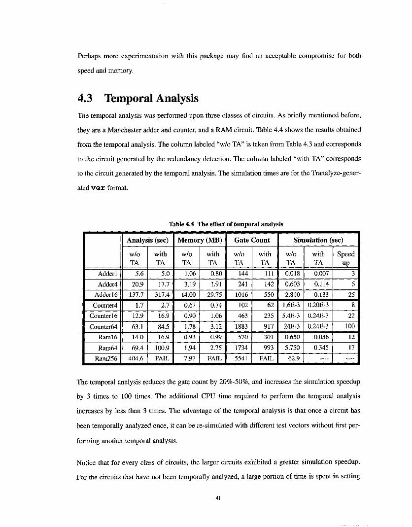
4.3 Temporal Analysis
The temporal analysis was performed upon three classes of circuits. As briefly mentioned before,
they are a Manchester adder and counter, and a RAM circuit. Table 4.4 shows the results obtained
from the temporal analysis. The column labeled "w/o TA" is taken from Table 4.3 and corresponds
to the circuit generated by the redundancy detection. The column labeled "with TA" corresponds
to the circuit generated by the temporal analysis. The simulation times are for the Tranalyze-gener-
ated ~re~" format.
Adderl
Adder4
Adderl6
Counter4
Counter16
Counter64
Raml6
Ram64
Ram256
Table 4.4 The effect of temporal analysis
Analysis (sec)
w/o withTA TA
5.6 5.0
20.9 17.7
137.7 317.4
1.7 2.7
12.9 16.9
63.1 ’84.5
14.0 16.9
69.4 100.9
404.6 FAIL
Memory (MB)
w/o withTA TA
1.06 0.80
3.19 1.91
14,00 29.75
0.67 0.74
0.90 1.06
1.78 3.12
0.93 0.99
1.94 2.75
7.97 FAIL
Gate Count
w/o withTA TA
144 111
241 142
1016 550
102 62
463 235
1883 917
570 301
1734 993
5541 FAIL
Simulation (sec)
w/oTA
0.018
0.603
2.810
1.6E-3
5.4E-3
24E-3
0.650
5.750
62.9
with SpeedTA up
0.007 3
0.114 5
0.133 25
0.20E-3 8
0.24E-3 22
0.24E-3 100
0.056 12
0.345 17
The temporal analysis reduces the gate count by 20%-50%, and increases the simulation speedup
by 3 times to 100 times. The additional CPU time required to perform the temporal analysis
increases by less than 3 times. The advantage of the temporal analysis is that once a circuit has
been temporally analyzed once, it can be re-simulated with different test vectors without first per-
forming another temporal analysis.
Notice that for every class of circuits, the larger circuits exhibited a greater simulation speedup.
For the circuits that have not been temporally analyzed, a large portion of time is spent in setting
41
up the simulation for each clock phase. As the circuit size grows larger, more time may be spent in
the setup mode. After temporal analysis, the simulator significantly reduces this setup time, thus
improving the simulation. Larger circuits should display an even greater speedup after temporal
analysis.
During the redundancy analysis, the BDD node limit was set to 0.5 million nodes. If this limit
were reached, the analysis would terminate and return the circuit with some redundancies
removed. During the temporal analysis, the entire analysis must be completed to produce a valid
circuit. Thus, the limit for temporal analysis is set much larger to 1.5 million nodes. However, this
limit was not large enough for the 256-bit RAM as it reached the limit and did not successfully
complete.
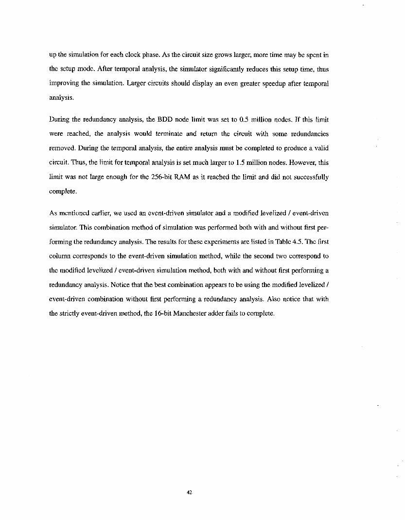
As mentioned earlier, we used an event-driven simulator and a modified levelized / event-driven
simulator. This combination method of simulation was performed both with and without first per-
forming the redundancy analysis. The results for these experiments are listed in Table 4.5. The first
column corresponds to the event-driven simulation method, while the second two correspond to
the modified levelized / event-driven simulation method, both with and without first performing a
redundancy analysis. Notice that the best combination appears to be using the modified levelized /
event-driven combination without first performing a redundancy analysis. Also notice that with
the strictly event-driven method, the 16-bit Manchester adder fails to complete.
42
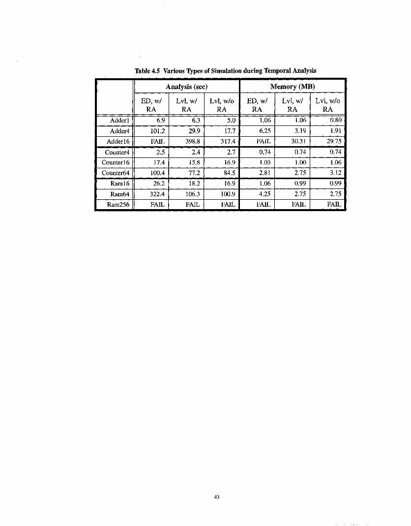
Table 4.5 Various Types of Simulation during Temporal Analysis
Analysis (sec) Memory (MB)
Ram256
ED, w/ Lvl, w/ Lvl, w/o ED, w/ Lvl, w/ Lvl, w/oRA RA RA RA RA RA
Adderl 6.9 6.3 5.0 1.06 1.06 0.80
Adder4 101.2 29.9 17.7 6.25 3.19 1.91
Adder 16 FAIL 398.8 317.4 FAIL 30.31 29.75
Counter4 2.5 2.4 2.7 0.74 0.74 0.74
Counterl6 17.4 15.8 16.9 1.03 1.00 1.06
Counter64 100.4 77.2 84.5 2.81 2.75 3.12
Raml6 26.2 18.2 16.9 1.06 0.99 0.99
Ram64 322.4 106.3 100.9 4.25 2.75 2.75
FAILFAIL FAIL FAIL FAIL FAIL
43
Section 5
Conclusions and Future Work
We have developed a tool that performs a temporal analysis on gate-level circuits. The net effect of
this temporal analysis is that the clocks are abstracted from the circuit, and a new gate-level circuit
is produced. This new circuit has applications in simulation, formal hardware verification, and
reverse engineering of pre-existing circuits.
We have observed a significant reduction in the size of the circuit after a temporal analysis is per-
formed. The speedup of the simulation ranges from 3X-100X, with speedup increasing as the size
of the circuit increases.
One major limitation we discovered is the memory needed to perform the analysis. Our tool uses
BDDs, which can easily become very large if a non-optimal variable ordering scheme is used.
Therefore, we should focus future efforts on ensuring a good variable ordering to control the size
of the BDD. In order to represent each of the state nodes, our temporal analysis generates new
variables for nearly all unit delays in the original circuit. Minor heuristics are used in the presimu-
lation step, as described in section 2.2.1, to prevent some variables from being introduced. Some
of the unit delays do not represent states that are important for our temporal analysis. Thus we
would like to be able to identify all of the state nodes in the circuit, and only create new variables
for these nodes.
Currently, our temporal analysis samples outputs at a discrete point in time. The formal verifica-
tion strategy used by our group requires outputs to be valid over a range of time, so it would be
advantageous for us to extend our temporal analysis so that outputs are sampled over a range of
time.
Finally, by performing a temporal analysis on sequential circuits, we have generated a more
abstract circuit. We would like to extend our analysis so that we can extract out an even more
abstract circuit. The next logical step would be to extract a finite state machine from the temporally
analyzed circuit.
45
Bibliography
[1] M. Abramovici, M.A. Breuer, and A.D. Friedman. Digital Systems Testing and Testable
Design. New York: W.H. Freeman and Company, 1990.
[2] Z. Barzilai, J. L. Carter, B. K. Rosen, and J. D. Rutledge. "HSS--A High-Speed Simulator,"
IEEE Transactions on Computer-Aided Design of Integrated Circuits and Systems, Vol. 6,
No. 4, July 1987, pp. 601-617.
[3] K.S. Brace. Ordered Binary Decision Diagrams for Optimization in Symbolic Switch-Level
Analysis of MOS Circuits. Ph.D. thesis, Carnegie Mellon University, 1992.
[4] K.S. Brace, R. E. Bryant, and R. L. Rudell. "Efficient Implementation of a BDD package,"
27th A CM/IEEE Design Automation Conference Proceedings, 1990, pp. 40-45,
[5] K.S. Brace. Personal Communication, 1993.
[6] R.E. Bryant. "Graph-Based Algorithms for Boolean Function Manipulation," IEEE Trans-
actions on Computers, August 1986, pp. 677-691.
[7] R.E. Bryant, D. Beatty, K. Brace, K. Cho, and T. Sheffler. "COSMOS: A Compiled Simula-
tor for MOS Circuits," 24th ACM/IEEE Design Automation Conference Proceedings, 1987,
pp. 9-16.
[8] R. E. Bryant. "Symbolic Simulation -- Techniques and Applications," 27th ACM/1EEE
Design Automation Conference Proceedings, 1990, pp. 517-521.
[9] R. E. Bryant. "Extraction of Gate Level Models from Transistor Circuits by Four-Valued
Symbolic Analysis," Proceedings of the IEEE/A CM International Conference on Computer
Aided Design, 1991, pp. 350-353.
[10] R. Gamier and J. Taylor. Discrete Mathematics for New Technologies. Bristol, England:
Adam Hilger, 1992.
[11] Timothy Kam and P.A. Subrahmanyam. "Comparing Layouts with HDL Models: A Formal
Verification Technique," Proceedings of the International Conference on Computer Design,
1992, pp. 588-591.
[12] D.M. Lewis. "A Hierarchical Compiled Code Event-Driven Logic Simulator," IEEE Trans-
actions on Computer-Aided Design of Integrated Circuits and Systems, Vol.10, No.6, June
1991, pp.726-737.
[13] C. A. Mead and L. A. Conway. Introduction to VLSI Systems. Reading, Massachusetts:
Addison-Wesley Publishing Company, 1980.
[14] S. Malik, A. R. Wang, R. K. Brayton, and A. Sangiovanni-Vincentelli. "Logic Verification
using Binary Decision Diagrams in a Logic Synthesis Environment," Proceedings of the
IEEE/ACM International Conference on Computer Aided Design, 1988, pp. 6-9.
[15] R. Razdan, G. Bischoff, and E. Ulrich. "Exploitation of Periodicity in Logic Simulation of
Synchronous Circuits," Proceedings of the IEEE/ACM International Conference on Com-
puter Aided Design, 1990, pp. 62-65.
[16] R. Razdan and G. Bischoff. "Clock Suppression Techniques for Synchronous Circuits,"
IEEE Transactions on Computer-Aided Design of lntegrated Circuits and Systems, Vol.12,
No.10, October 1993, pp.1547-1556.
[17] Richard Rudell. "Dynamic Variable Ordering for Ordered Binary Decision Diagrams," Pro-
ceedings of the IEEE/ACM International Conference on Computer Aided Design, 1993, pp.
42-47.
[18] C-J. Seger and R. E. Bryant. "Modeling of Circuit Delays in Symbolic Simulation," IMEC-
IFIP International Workshop on Applied Formal Methods for Correct VLSI Design, 1989,
pp. 766-779.
47
[19] Y. Takamine, S. Miyamoto, S. Nagashima, M. Miyoshi, and S. Kawabe. "Clock Event Sup-
pression Algorithm of VELVET And Its Application to S-820 Development," 25th ACM/
IEEE Design Automation Conference Proceedings, 1988, pp. 716-719.
[20] E. Ulrich and D. Hebert. "Speed and Accuracy in Digital Network Simulation Based on
Structural Modeling," 19th A CM/IEEE Design Automation Conference Proceedings, 1982,
pp. 587-593.
[21] E. Ulrich. "A Design Verification Methodology based on Concurrent Simulation and Clock
Suppression," 20th A CM/IEEE Design Automation Conference Proceedings, 1983, pp. 709-
712.
[22] E. Ulrich, M, Kearney, J. Tellier, and S. Demba. "Design Verification for very large digital
networks based on Concurrent Simulation and Clock Suppression," Proceedings of the
International Conference on Computer Design, 1983, pp. 277-280.
[23] T. Weber and F. Somenzi. "Periodic Signal Suppression in a Concurrent Fault Simulator,"
Proceedings of The European Conference on Design Automation, 1991, pp. 565-569.
48

49