automotive adjustable voltage reference - … · automotive adjustable voltage reference datasheet...
TRANSCRIPT
This is information on a product in full production.
December 2017 DocID4467 Rev 12 1/21
TL431TL432
Automotive adjustable voltage reference
Datasheet - production data
Features
AEC-Q100 qualified
Adjustable output voltage: 2.5 to 36 V
Sink current capability: 1 to 100 mA
Typical output impedance: 0.22 Ω
1% and 2% voltage precision
Automotive temp. range -40 °C to +125 °C
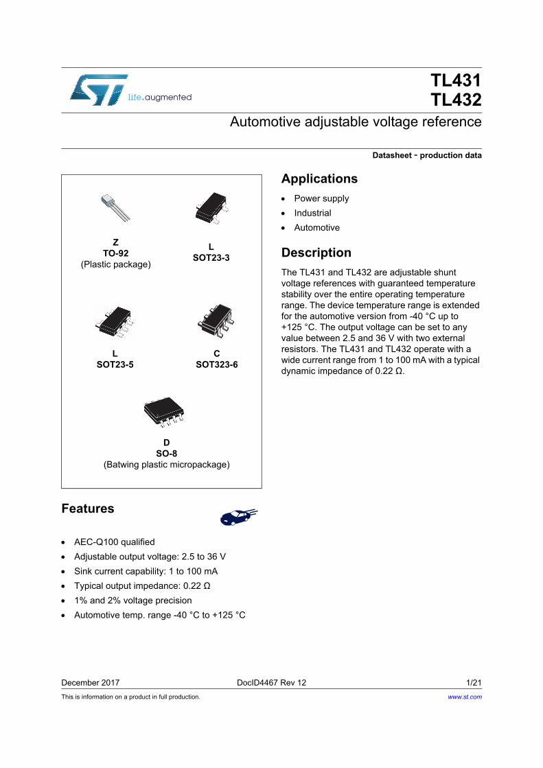
Applications
Power supply
Industrial
Automotive
Description
The TL431 and TL432 are adjustable shunt voltage references with guaranteed temperature stability over the entire operating temperature range. The device temperature range is extended for the automotive version from -40 °C up to +125 °C. The output voltage can be set to any value between 2.5 and 36 V with two external resistors. The TL431 and TL432 operate with a wide current range from 1 to 100 mA with a typical dynamic impedance of 0.22 Ω.
DSO-8
(Batwing plastic micropackage)
ZTO-92
(Plastic package)
LSOT23-3
LSOT23-5
CSOT323-6
www.st.com
Contents TL431, TL432
2/21 DocID4467 Rev 12
Contents
1 Schematic diagrams . . . . . . . . . . . . . . . . . . . . . . . . . . . . . . . . . . . . . . . . . 3
2 Absolute maximum ratings and operating conditions . . . . . . . . . . . . . 4
3 Electrical characteristics . . . . . . . . . . . . . . . . . . . . . . . . . . . . . . . . . . . . . 5
Reference input voltage deviation over temperature range . . . . . . . . . . . . . . . . . . 7
4 Package information . . . . . . . . . . . . . . . . . . . . . . . . . . . . . . . . . . . . . . . . 11
4.1 SO-8 package information . . . . . . . . . . . . . . . . . . . . . . . . . . . . . . . . . . . . 12
4.2 TO-92 ammopack and tape and reel package information . . . . . . . . . . . 13
4.3 TO-92 (bulk) package information . . . . . . . . . . . . . . . . . . . . . . . . . . . . . . 14
4.4 SOT23-3 package information . . . . . . . . . . . . . . . . . . . . . . . . . . . . . . . . . 15
4.5 SOT23-5 package information . . . . . . . . . . . . . . . . . . . . . . . . . . . . . . . . . 16
4.6 SOT323-6 package information . . . . . . . . . . . . . . . . . . . . . . . . . . . . . . . . 17
5 Ordering information . . . . . . . . . . . . . . . . . . . . . . . . . . . . . . . . . . . . . . . 18
6 Revision history . . . . . . . . . . . . . . . . . . . . . . . . . . . . . . . . . . . . . . . . . . . 20
DocID4467 Rev 12 3/21
TL431, TL432 Schematic diagrams
21
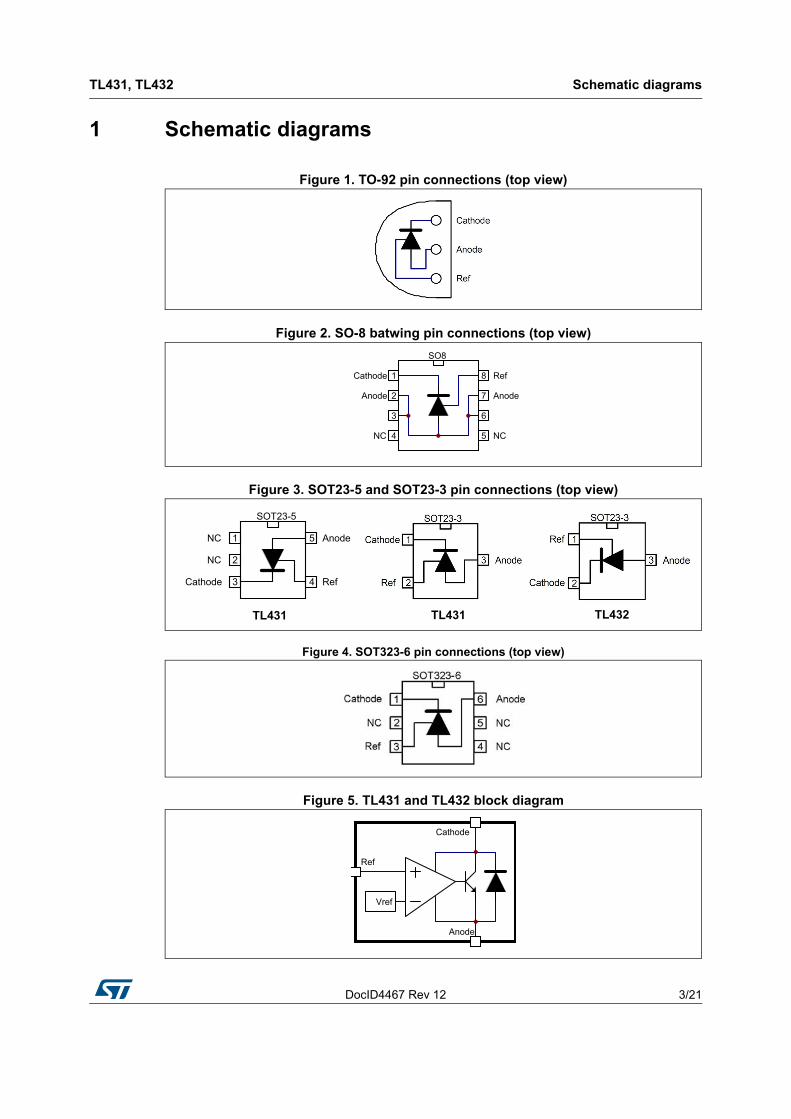
1 Schematic diagrams
Figure 1. TO-92 pin connections (top view)
Figure 2. SO-8 batwing pin connections (top view)
Figure 3. SOT23-5 and SOT23-3 pin connections (top view)
Figure 4. SOT323-6 pin connections (top view)
Figure 5. TL431 and TL432 block diagram
SO8
Anode
Cathode Ref1
2
3
7
8
4
6
NC5
Anode
NC
SOT23-3SOT23-5
NC
NC
Cathode Ref
Anode1
2
3 4
5 Cathode
Ref Anode
1
2 3
TL431 TL431 TL432
Anode
Cathode
Vref
Ref
Absolute maximum ratings and operating conditions TL431, TL432
4/21 DocID4467 Rev 12
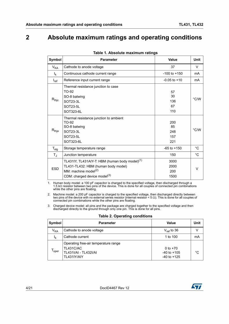
2 Absolute maximum ratings and operating conditions
Table 1. Absolute maximum ratings
Symbol Parameter Value Unit
VKA Cathode to anode voltage 37 V
Ik Continuous cathode current range -100 to +150 mA
Iref Reference input current range -0.05 to +10 mA
Rthjc
Thermal resistance junction to case
TO-92
SO-8 batwing
SOT23-3L
SOT23-5L
SOT323-6L
5730
136
67
110
°C/W
Rthja
Thermal resistance junction to ambientTO-92SO-8 batwing
SOT23-3L
SOT23-5L
SOT323-6L
20085
248
157
221
°C/W
Tstg Storage temperature range -65 to +150 °C
TJ Junction temperature 150 °C
ESD
TL431IY, TL431AIY-T: HBM (human body model)(1)
TL431-TL432: HBM (human body model)
MM: machine model(2)
CDM: charged device model(3)
1. Human body model: a 100 pF capacitor is charged to the specified voltage, then discharged through a 1.5 kresistor between two pins of the device. This is done for all couples of connected pin combinations while the other pins are floating.
2. Machine model: a 200 pF capacitor is charged to the specified voltage, then discharged directly between two pins of the device with no external series resistor (internal resistor < 5 ). This is done for all couples of connected pin combinations while the other pins are floating.
3. Charged device model: all pins and the package are charged together to the specified voltage and then discharged directly to the ground through only one pin. This is done for all pins.
3000
2000
200
1500
V
Table 2. Operating conditions
Symbol Parameter Value Unit
VKA Cathode to anode voltage Vref to 36 V
Ik Cathode current 1 to 100 mA
Toper
Operating free-air temperature range
TL431C/ACTL431I/AI - TL432I/AITL431IY/AIY
0 to +70-40 to +105-40 to +125
°C

DocID4467 Rev 12 5/21
TL431, TL432 Electrical characteristics
21
3 Electrical characteristics
Table 3. TL431C (Tamb = 25 °C unless otherwise specified)
Symbol ParameterTL431C TL431AC
UnitMin. Typ. Max. Min. Typ. Max.
Vref
Reference input voltage
VKA = Vref, Ik = 10 mA, Tamb = 25 °CTmin Tamb Tmax
2.442.423
2.495-
2.552.567
2.472.453
2.495-
2.522.537
V
Vref
Reference input voltage deviation overtemperature
range (1)
VKA = Vref, Ik = 10 mA, Tmin Tamb Tmax - 3 17 - 3 15mV
Ratio of change in reference input voltage to change in cathode to anode voltage
Ik = 10 mA - VKA = 10 V to Vref VKA = 36 V to 10 V
-2.7-2
-1.4-1
-
-
-2.7-2
-1.4-1
-
-
mV/V
Iref
Reference input currentIk = 10 mA, R1 = 10 k, R2 =
Tamb = 25 °CTmin Tamb Tmax
-
-
1.8
-4
5.2-
-
1.8
-4
5.2
µA
Iref
Reference input current deviation overtemperature range
Ik = 10 mA, R1 = 10 k, R2 =Tmin Tamb Tmax - 0.4 1.2 - 0.4 1.2
µA
IminMinimum cathode current for regulation
VKA = Vref-
0.5 1-
0.5 0.6mA
Ioff Off-state cathode current - 2.6 1000 - 2.6 1000 nA
ZKADynamic impedance(2)
VKA = Vref, Ik = 1 to 100 mA, f 1 kHZ - 0.22 0.5 - 0.22 0.5
1. See definition of Section : Reference input voltage deviation overtemperature range.
2. The dynamic impedance is defined as ZKA=
VrefVka------------
VKA
Ik----------------
Electrical characteristics TL431, TL432
6/21 DocID4467 Rev 12
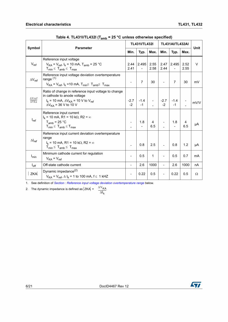
Table 4. TL431I/TL432I (Tamb = 25 °C unless otherwise specified)
Symbol ParameterTL431I/TL432I TL431AI/TL432AI
UnitMin. Typ. Max. Min. Typ. Max.
Vref
Reference input voltage
VKA = Vref, Ik = 10 mA, Tamb = 25 °CTmin Tamb Tmax
2.442.41
2.495-
2.552.58
2.472.44
2.495-
2.522.55
V
Vref
Reference input voltage deviation overtemperature range (1)
VKA = Vref, Ik =10 mA, Tmin Tamb Tmax- 7 30 - 7 30 mV
Ratio of change in reference input voltage to change in cathode to anode voltage
Ik = 10 mA, VKA = 10 V to Vref VKA = 36 V to 10 V
-2.7-2
-1.4-1
-
-
-2.7-2
-1.4-1
-
-mV/V
Iref
Reference input current Ik = 10 mA, R1 = 10 k, R2 =
Tamb = 25 °CTmin Tamb Tmax
-
-
1.8-
46.5
-
-
1.8-
46.5
µA
Iref
Reference input current deviation overtemperature range
Ik = 10 mA, R1 = 10 k, R2 = Tmin Tamb Tmax
- 0.8 2.5 - 0.8 1.2 µA
IminMinimum cathode current for regulation
VKA = Vref- 0.5 1 - 0.5 0.7 mA
Ioff Off-state cathode current - 2.6 1000 - 2.6 1000 nA
ZKADynamic impedance(2)
VKA = Vref, Ik = 1 to 100 mA, f 1 kHZ- 0.22 0.5 - 0.22 0.5
1. See definition of Section : Reference input voltage deviation overtemperature range below.
2. The dynamic impedance is defined as ZKA=
VrefVka------------
VKA
Ik----------------
DocID4467 Rev 12 7/21
TL431, TL432 Electrical characteristics
21
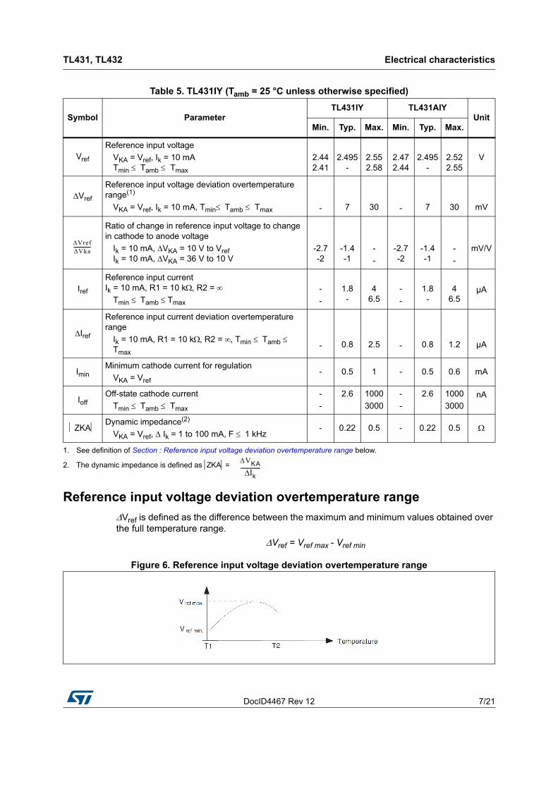
Reference input voltage deviation overtemperature range
Vref is defined as the difference between the maximum and minimum values obtained over the full temperature range.
Vref = Vref max - Vref min
Figure 6. Reference input voltage deviation overtemperature range
Table 5. TL431IY (Tamb = 25 °C unless otherwise specified)
Symbol ParameterTL431IY TL431AIY
UnitMin. Typ. Max. Min. Typ. Max.
Vref
Reference input voltage
VKA = Vref, Ik = 10 mATmin Tamb Tmax
2.442.41
2.495-
2.552.58
2.472.44
2.495-
2.522.55
V
Vref
Reference input voltage deviation overtemperature range(1)
VKA = Vref, Ik = 10 mA, Tmin Tamb Tmax - 7 30 - 7 30 mV
Ratio of change in reference input voltage to change in cathode to anode voltage
Ik = 10 mA, VKA = 10 V to Vref Ik = 10 mA, VKA = 36 V to 10 V
-2.7-2
-1.4-1
-
-
-2.7-2
-1.4-1
-
-
mV/V
Iref
Reference input current Ik = 10 mA, R1 = 10 k, R2 =
Tmin Tamb Tmax
-
-
1.8-
46.5
-
-
1.8-
46.5
µA
Iref
Reference input current deviation overtemperature range
Ik = 10 mA, R1 = 10 k, R2 = Tmin Tamb Tmax
- 0.8 2.5 - 0.8 1.2 µA
IminMinimum cathode current for regulation
VKA = Vref- 0.5 1 - 0.5 0.6 mA
IoffOff-state cathode current
Tmin Tamb Tmax
-
-
2.6 1000
3000
-
-
2.6 1000
3000nA
ZKADynamic impedance(2)
VKA = Vref, Ik = 1 to 100 mA, F 1 kHz- 0.22 0.5 - 0.22 0.5
1. See definition of Section : Reference input voltage deviation overtemperature range below.
2. The dynamic impedance is defined as ZKA=
VrefVka------------
VKA
Ik----------------
Electrical characteristics TL431, TL432
8/21 DocID4467 Rev 12
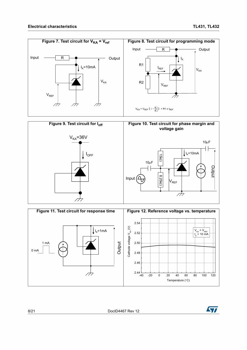
Figure 7. Test circuit for VKA = Vref Figure 8. Test circuit for programming mode
Input
VKA
VREF
IK=10mA
OutputR
VKA = VREF + R1 x IREF 1 R1R2-------+
Input
VKA
VREF
IK
R1
R2
IREF
R Output
Figure 9. Test circuit for Ioff Figure 10. Test circuit for phase margin and voltage gain
VKA=36V
IOFF
InputVREF
IK=10mA
Ou
tput
10F
10F
15k
8.25k
Figure 11. Test circuit for response time Figure 12. Reference voltage vs. temperature
IK=1mA
Ou
tpu
t
0 mA
1 mA
-40 -20 0 20 40 60 80 100 1202.44
2.46
2.48
2.50
2.52
2.54
VKA
= VREF
IK = 10 mA
Cat
hode
vo
ltag
e V
KA (
V)
Temperature (C)
DocID4467 Rev 12 9/21
TL431, TL432 Electrical characteristics
21
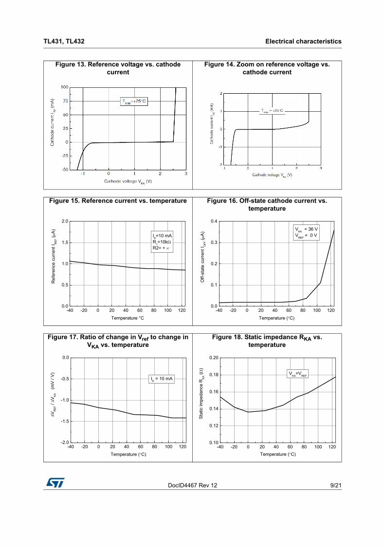
Figure 13. Reference voltage vs. cathode current
Figure 14. Zoom on reference voltage vs. cathode current
Figure 15. Reference current vs. temperature Figure 16. Off-state cathode current vs. temperature
-40 -20 0 20 40 60 80 100 1200.0
0.5
1.0
1.5
2.0
IK=10 mA
R1=10k
R2= +
Re
fere
nce
cur
rent
IR
EF (A
)
Temperature °C
-40 -20 0 20 40 60 80 100 1200.0
0.1
0.2
0.3
0.4
VKA
= 36 VV
REF = 0 V
Off
-sta
te c
urre
nt
I OF
F (A
)
Temperature (C)
Figure 17. Ratio of change in Vref to change in VKA vs. temperature
Figure 18. Static impedance RKA vs. temperature
-40 -20 0 20 40 60 80 100 120-2.0
-1.5
-1.0
-0.5
0.0
IK = 10 mA
VR
EF /
V
KA
(m
V /
V)
Temperature (C)
-40 -20 0 20 40 60 80 100 1200.10
0.12
0.14
0.16
0.18
0.20
VKA
=VREF
Sta
tic im
ped
ance
RK
A (
)
Temperature (C)
Electrical characteristics TL431, TL432
10/21 DocID4467 Rev 12
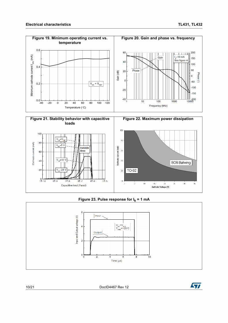
Figure 19. Minimum operating current vs. temperature
Figure 20. Gain and phase vs. frequency
-40 -20 0 20 40 60 80 100 1200.0
0.2
0.4
0.6
VKA
= VREF
Min
imum
cat
hod
e cu
rren
t I M
IN (
mA
)
Temperature (C)
Figure 21. Stability behavior with capacitive loads
Figure 22. Maximum power dissipation
Figure 23. Pulse response for Ik = 1 mA
DocID4467 Rev 12 11/21
TL431, TL432 Package information
21
4 Package information
In order to meet environmental requirements, ST offers these devices in different grades of ECOPACK® packages, depending on their level of environmental compliance. ECOPACK® specifications, grade definitions and product status are available at: www.st.com. ECOPACK® is an ST trademark.
Package information TL431, TL432
12/21 DocID4467 Rev 12
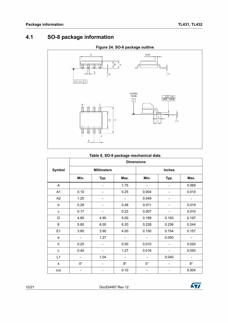
4.1 SO-8 package information
Figure 24. SO-8 package outline
Table 6. SO-8 package mechanical data
Symbol
Dimensions
Millimeters Inches
Min. Typ. Max. Min. Typ. Max.
A - 1.75 - - 0.069
A1 0.10 - 0.25 0.004 - 0.010
A2 1.25 - - 0.049 - -
b 0.28 - 0.48 0.011 - 0.019
c 0.17 - 0.23 0.007 - 0.010
D 4.80 4.90 5.00 0.189 0.193 0.197
E 5.80 6.00 6.20 0.228 0.236 0.244
E1 3.80 3.90 4.00 0.150 0.154 0.157
e - 1.27 - - 0.050 -
h 0.25 - 0.50 0.010 - 0.020
L 0.40 - 1.27 0.016 - 0.050
L1 - 1.04 - - 0.040 -
k 0° - 8° 0° - 8°
ccc - - 0.10 - - 0.004
DocID4467 Rev 12 13/21
TL431, TL432 Package information
21
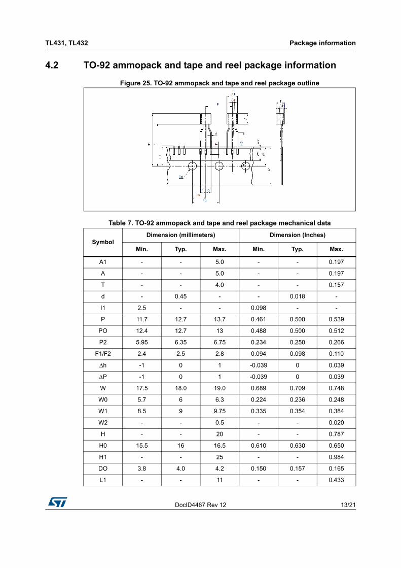
4.2 TO-92 ammopack and tape and reel package information
Figure 25. TO-92 ammopack and tape and reel package outline
Table 7. TO-92 ammopack and tape and reel package mechanical data
SymbolDimension (millimeters) Dimension (Inches)
Min. Typ. Max. Min. Typ. Max.
A1 - - 5.0 - - 0.197
A - - 5.0 - - 0.197
T - - 4.0 - - 0.157
d - 0.45 - - 0.018 -
I1 2.5 - - 0.098 - -
P 11.7 12.7 13.7 0.461 0.500 0.539
PO 12.4 12.7 13 0.488 0.500 0.512
P2 5.95 6.35 6.75 0.234 0.250 0.266
F1/F2 2.4 2.5 2.8 0.094 0.098 0.110
h -1 0 1 -0.039 0 0.039
P -1 0 1 -0.039 0 0.039
W 17.5 18.0 19.0 0.689 0.709 0.748
W0 5.7 6 6.3 0.224 0.236 0.248
W1 8.5 9 9.75 0.335 0.354 0.384
W2 - - 0.5 - - 0.020
H - - 20 - - 0.787
H0 15.5 16 16.5 0.610 0.630 0.650
H1 - - 25 - - 0.984
DO 3.8 4.0 4.2 0.150 0.157 0.165
L1 - - 11 - - 0.433
Package information TL431, TL432
14/21 DocID4467 Rev 12
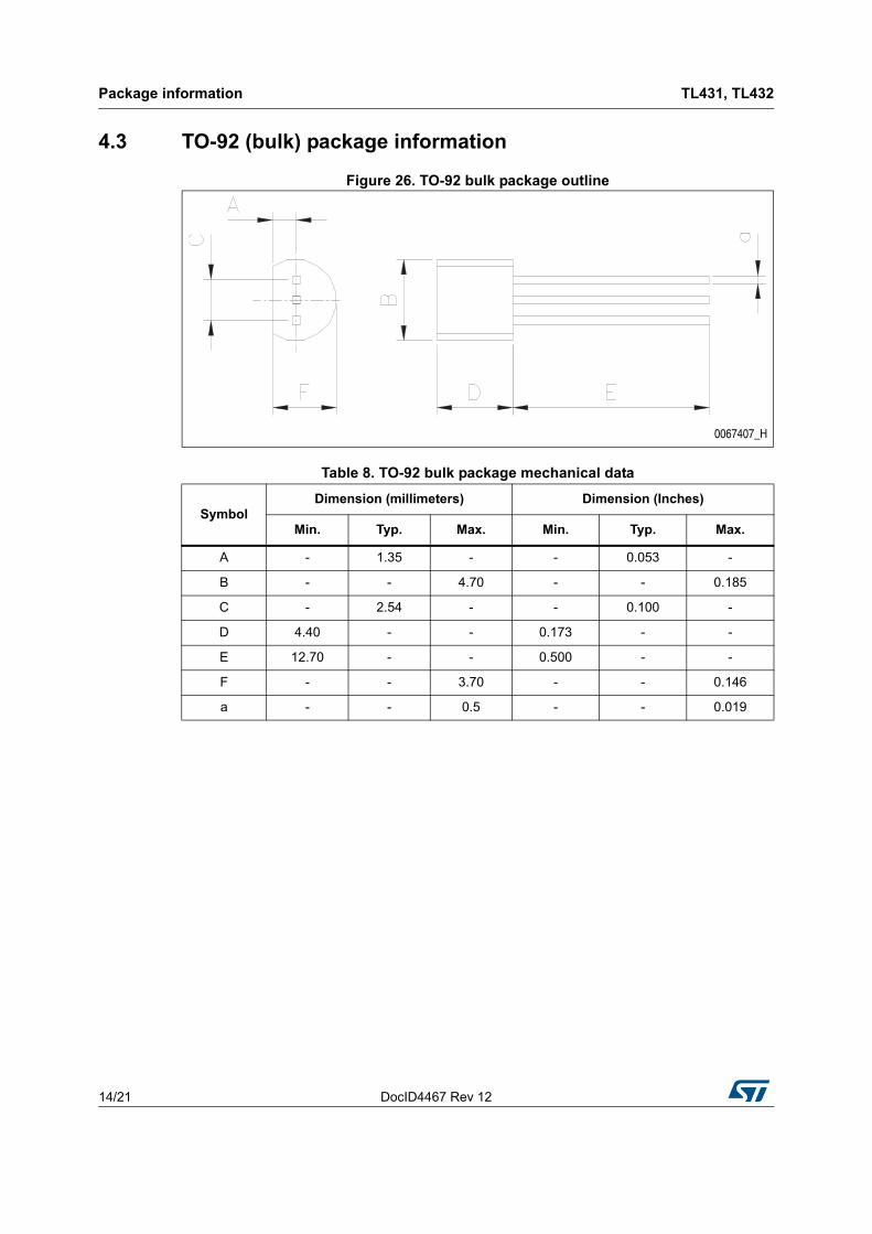
4.3 TO-92 (bulk) package information
Figure 26. TO-92 bulk package outline
Table 8. TO-92 bulk package mechanical data
SymbolDimension (millimeters) Dimension (Inches)
Min. Typ. Max. Min. Typ. Max.
A - 1.35 - - 0.053 -
B - - 4.70 - - 0.185
C - 2.54 - - 0.100 -
D 4.40 - - 0.173 - -
E 12.70 - - 0.500 - -
F - - 3.70 - - 0.146
a - - 0.5 - - 0.019
0067407_H
DocID4467 Rev 12 15/21
TL431, TL432 Package information
21
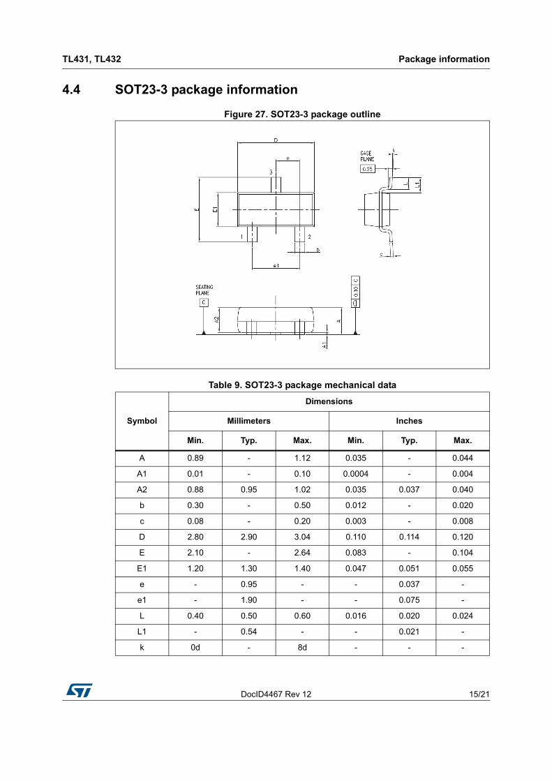
4.4 SOT23-3 package information
Figure 27. SOT23-3 package outline
Table 9. SOT23-3 package mechanical data
Symbol
Dimensions
Millimeters Inches
Min. Typ. Max. Min. Typ. Max.
A 0.89 - 1.12 0.035 - 0.044
A1 0.01 - 0.10 0.0004 - 0.004
A2 0.88 0.95 1.02 0.035 0.037 0.040
b 0.30 - 0.50 0.012 - 0.020
c 0.08 - 0.20 0.003 - 0.008
D 2.80 2.90 3.04 0.110 0.114 0.120
E 2.10 - 2.64 0.083 - 0.104
E1 1.20 1.30 1.40 0.047 0.051 0.055
e - 0.95 - - 0.037 -
e1 - 1.90 - - 0.075 -
L 0.40 0.50 0.60 0.016 0.020 0.024
L1 - 0.54 - - 0.021 -
k 0d - 8d - - -
Package information TL431, TL432
16/21 DocID4467 Rev 12
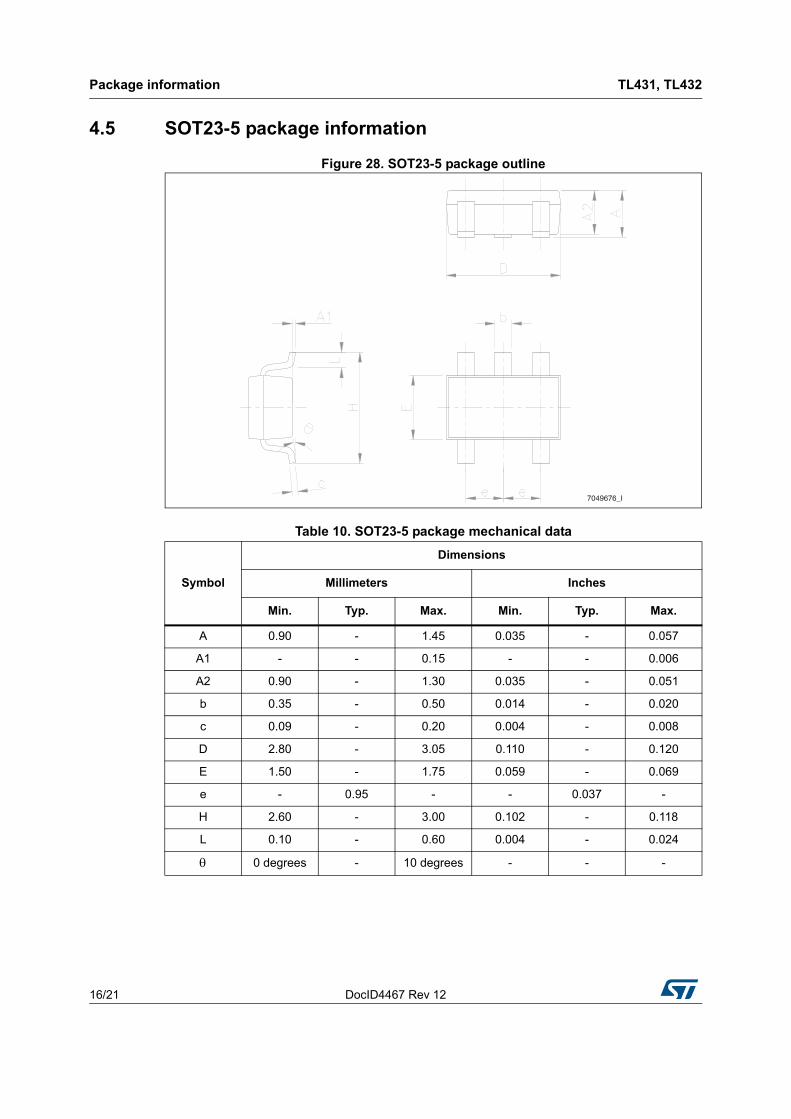
4.5 SOT23-5 package information
Figure 28. SOT23-5 package outline
Table 10. SOT23-5 package mechanical data
Symbol
Dimensions
Millimeters Inches
Min. Typ. Max. Min. Typ. Max.
A 0.90 - 1.45 0.035 - 0.057
A1 - - 0.15 - - 0.006
A2 0.90 - 1.30 0.035 - 0.051
b 0.35 - 0.50 0.014 - 0.020
c 0.09 - 0.20 0.004 - 0.008
D 2.80 - 3.05 0.110 - 0.120
E 1.50 - 1.75 0.059 - 0.069
e - 0.95 - - 0.037 -
H 2.60 - 3.00 0.102 - 0.118
L 0.10 - 0.60 0.004 - 0.024
0 degrees - 10 degrees - - -
7049676_I
DocID4467 Rev 12 17/21
TL431, TL432 Package information
21
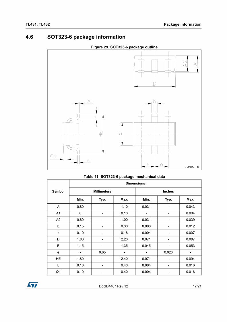
4.6 SOT323-6 package information
Figure 29. SOT323-6 package outline
Table 11. SOT323-6 package mechanical data
Symbol
Dimensions
Millimeters Inches
Min. Typ. Max. Min. Typ. Max.
A 0.80 - 1.10 0.031 - 0.043
A1 0 - 0.10 - - 0.004
A2 0.80 - 1.00 0.031 - 0.039
b 0.15 - 0.30 0.006 - 0.012
c 0.10 - 0.18 0.004 - 0.007
D 1.80 - 2.20 0.071 - 0.087
E 1.15 - 1.35 0.045 - 0.053
e - 0.65 - - 0.026 -
HE 1.80 - 2.40 0.071 - 0.094
L 0.10 - 0.40 0.004 - 0.016
Q1 0.10 - 0.40 0.004 - 0.016
7095021_E
Ordering information TL431, TL432
18/21 DocID4467 Rev 12
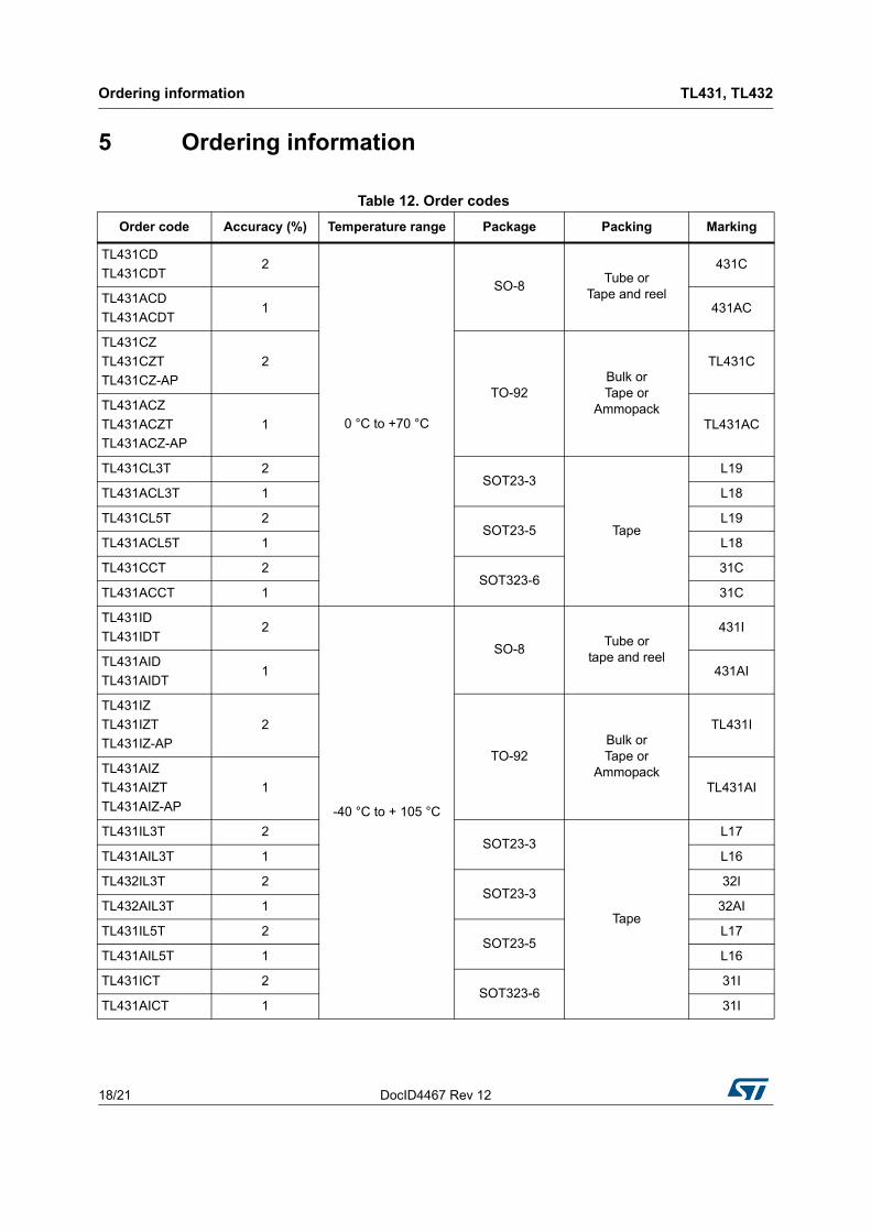
5 Ordering information
Table 12. Order codes
Order code Accuracy (%) Temperature range Package Packing Marking
TL431CD
TL431CDT2
0 °C to +70 °C
SO-8Tube or
Tape and reel
431C
TL431ACD
TL431ACDT1 431AC
TL431CZ
TL431CZT
TL431CZ-AP
2
TO-92Bulk orTape or
Ammopack
TL431C
TL431ACZ
TL431ACZT
TL431ACZ-AP
1 TL431AC
TL431CL3T 2SOT23-3
Tape
L19
TL431ACL3T 1 L18
TL431CL5T 2SOT23-5
L19
TL431ACL5T 1 L18
TL431CCT 2SOT323-6
31C
TL431ACCT 1 31C
TL431ID
TL431IDT2
-40 °C to + 105 °C
SO-8Tube or
tape and reel
431I
TL431AID
TL431AIDT1 431AI
TL431IZ
TL431IZT
TL431IZ-AP
2
TO-92Bulk orTape or
Ammopack
TL431I
TL431AIZ
TL431AIZT
TL431AIZ-AP
1 TL431AI
TL431IL3T 2SOT23-3
Tape
L17
TL431AIL3T 1 L16
TL432IL3T 2SOT23-3
32I
TL432AIL3T 1 32AI
TL431IL5T 2SOT23-5
L17
TL431AIL5T 1 L16
TL431ICT 2SOT323-6
31I
TL431AICT 1 31I
DocID4467 Rev 12 19/21
TL431, TL432 Ordering information
21
TL431IYD(1)
TL431IYDT(1) 2
-40 °C to + 125 °CSO-8
(Automotive grade level)
Tube ortape and reel
431IY
TL431AIYD(1)
TL431AIYDT(1) 1 431AIY
1. Qualification and characterization according to AEC Q100 and Q003 or equivalent, advanced screening according to AEC Q001 and Q 002 or equivalent.
Table 12. Order codes (continued)
Order code Accuracy (%) Temperature range Package Packing Marking
Revision history TL431, TL432
20/21 DocID4467 Rev 12
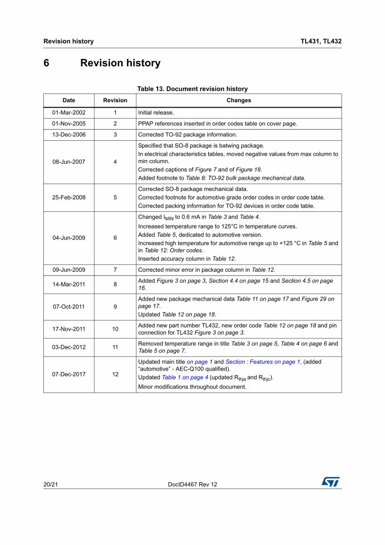
6 Revision history
Table 13. Document revision history
Date Revision Changes
01-Mar-2002 1 Initial release.
01-Nov-2005 2 PPAP references inserted in order codes table on cover page.
13-Dec-2006 3 Corrected TO-92 package information.
08-Jun-2007 4
Specified that SO-8 package is batwing package.
In electrical characteristics tables, moved negative values from max column to min column.
Corrected captions of Figure 7 and of Figure 18.
Added footnote to Table 8: TO-92 bulk package mechanical data.
25-Feb-2008 5
Corrected SO-8 package mechanical data.
Corrected footnote for automotive grade order codes in order code table.
Corrected packing information for TO-92 devices in order code table.
04-Jun-2009 6
Changed IMIN to 0.6 mA in Table 3 and Table 4.
Increased temperature range to 125°C in temperature curves.
Added Table 5, dedicated to automotive version.
Increased high temperature for automotive range up to +125 °C in Table 5 and in Table 12: Order codes.
Inserted accuracy column in Table 12.
09-Jun-2009 7 Corrected minor error in package column in Table 12.
14-Mar-2011 8Added Figure 3 on page 3, Section 4.4 on page 15 and Section 4.5 on page 16.
07-Oct-2011 9Added new package mechanical data Table 11 on page 17 and Figure 29 on page 17.
Updated Table 12 on page 18.
17-Nov-2011 10Added new part number TL432, new order code Table 12 on page 18 and pin connection for TL432 Figure 3 on page 3.
03-Dec-2012 11Removed temperature range in title Table 3 on page 5, Table 4 on page 6 and Table 5 on page 7.
07-Dec-2017 12
Updated main title on page 1 and Section : Features on page 1, (added “automotive” - AEC-Q100 qualified).
Updated Table 1 on page 4 (updated Rthja and Rthjc).
Minor modifications throughout document.
DocID4467 Rev 12 21/21
TL431, TL432
21
IMPORTANT NOTICE – PLEASE READ CAREFULLY
STMicroelectronics NV and its subsidiaries (“ST”) reserve the right to make changes, corrections, enhancements, modifications, and improvements to ST products and/or to this document at any time without notice. Purchasers should obtain the latest relevant information on ST products before placing orders. ST products are sold pursuant to ST’s terms and conditions of sale in place at the time of order acknowledgement.
Purchasers are solely responsible for the choice, selection, and use of ST products and ST assumes no liability for application assistance or the design of Purchasers’ products.
No license, express or implied, to any intellectual property right is granted by ST herein.
Resale of ST products with provisions different from the information set forth herein shall void any warranty granted by ST for such product.
ST and the ST logo are trademarks of ST. All other product or service names are the property of their respective owners.
Information in this document supersedes and replaces information previously supplied in any prior versions of this document.
© 2017 STMicroelectronics – All rights reserved