avalanche photodiodes in submicron cmos technologies …cdn.intechweb.org/pdfs/14343.pdf · 11...
TRANSCRIPT

11
Avalanche Photodiodes in Submicron CMOS Technologies for High-Sensitivity Imaging
Gian-Franco Dalla Betta1, Lucio Pancheri2, David Stoppa2, Robert Henderson3 and Justin Richardson3,4
1University of Trento 2Fondazione Bruno Kessler
3University of Edinburgh 4Dialog Semiconductor Ltd., Edinburgh
1,2Italy 3,4United Kingdom
1. Introduction
Vacuum based devices, such as Photo Multiplier Tubes (PMT) and Micro Channel Plates (MCP), have been for many years the sensors of choice for most applications calling for photon counting and timing (Renker, 2004). While providing very good sensitivity, noise and timing characteristics, these photodetectors feature a number of disadvantages: they are bulky, fragile, and sensitive to magnetic fields; they require very high operation voltages, and have large power consumption; in their high-performance models, providing good spatial resolution, they are still very expensive. For high-sensitivity imaging applications, suitable solutions are represented by CCD cameras coupled with either MCP Image Intensifiers (I-CCDs) or Electron Multipliers (EM-CCDs) (Dussault & Hoess, 2004). However, besides being very expensive, their performance is not completely satisfactory in extreme time resolved measurements. For reasons of cost, miniaturization, ruggedness, reliability, design flexibility, integration density, and signal processing capabilities, a fully solid-state solution (and, particularly, CMOS technology) would be highly desirable. Among the advanced CMOS image sensors so far reported, the most promising ones in terms of high sensitivity and fast timing are those based on Single Photon Avalanche Diodes (SPADs). SPADs are avalanche photodiodes operated in the so-called Geiger mode, i.e., biased above breakdown, so as to be sensitive to single photons (Cova et al., 1996). Although these sensors have been developed for more than 30 years, in particular owing to the group of Prof. Cova at Politecnico di Milano, and single devices have reached outstanding performance (Ghioni et al., 2007), only recently the perspective of making a SPAD-based camera has become feasible. The first SPAD-based pixel arrays in CMOS technology have been demonstrated only a few years ago (Rochas et al., 2003a), but since then further developments rapidly followed, also facilitated by the availability of commercial, High-Voltage CMOS technologies (HV-CMOS) aimed at integrated circuits for power electronics, as well as of specially tailored “imaging” processes, which have been boosted by the huge market of
www.intechopen.com

Advances in Photodiodes
226
mobile phone cameras. As a result, also submicron CMOS technologies with ever decreasing minimum feature size, down to 130nm, could be used for SPAD fabrication. The electro-optical characteristics of CMOS SPADs are not optimized in some respects, but their monolithic integration with readout electronics might offer several advantages for the design of low-cost and high-performance fully integrated imaging systems with time-resolved, single-photon detection capabilities. These devices can be used in many application fields: imaging in extreme low-level light conditions (night, caves, …), real time imaging of the motion of natural gravity-driven flows (snow avalanches, landslides, …), ranging and three-dimensional vision, biomedical and molecular biology (single molecule spectroscopy, luminescence microscopy, fluorescence lifetime imaging, etc.), scintillation detection in nuclear medicine (SPECT - Single Photon Emission Compute Tomography; PET - Positron Emission Tomography) and particle/nuclear physics, quantum cryptography, astronomy, adaptive optics, non invasive testing of VLSI circuits, to cite but a few. While a considerable number of CMOS image sensors based on SPADs have already been presented, CMOS Avalanche Photodiodes (APDs) operating in the linear regime have not evolved to the same extent. Only a few successful implementations have been proposed so far, and large arrays are not available yet. These devices could be interesting for some applications, especially in the detection of blue and UV light, where the noise factor of the device is small, whereas at larger wavelengths the noise is normally higher. In this Chapter, after reviewing basic operation principles, figures of merit, and state-of-the-art, we report on the design and experimental characterization of both Geiger- and linear-mode avalanche photodiodes devices fabricated in different submicron CMOS technologies. The electro-optical properties are evaluated, underlining the impact of technology scaling on the device characteristics. Moreover, we discuss the main design issues relevant to integrated read-out channels for SPADs to be used in active pixel sensor arrays for high-sensitivity imaging applications.
2. Operation principle
Avalanche photodiodes are p-n junction photodiodes purposely made to be operated at high electric fields in order to achieve an internal gain. In reverse biased photodiodes, the electric field increases with the applied voltage, causing the drift velocity and kinetic energy of charge carriers injected in the depletion region to increase. By doing so, an electron (or a hole) can reach an energy high enough to break a bond when colliding with lattice atoms, thus generating a new electron-hole pair, and losing part of its energy in this process, which is called impact ionization (Sze & Ng, 2007). Both the original carrier (electron or hole) and the secondary electron and hole will be accelerated by the electric field and possibly contribute to the generation of more electron-hole pairs, this resulting in a positive feedback loop which gradually increases the overall number of carriers, hence the term avalanche. Note that this applies both to optically generated carriers and to carriers generated by any other mechanism (e.g., thermally generated carriers). The magnitude of the avalanche phenomenon is governed by two concurrent factors: the carrier ionization rates, which are defined as the number of pairs created by a carrier per unit distance travelled, and the rate at which electrons and holes leave the high-field region and are collected at the device electrodes (Aull et al., 2002). Ionization rates are strongly increasing with the electric field. Although in silicon electrons have a higher ionization rate than holes, on average an electric field value of about 3×10⁵ V/cm is required to create one electron-hole pair per 1 μm
www.intechopen.com

Avalanche Photodiodes in Submicron CMOS Technologies for High-Sensitivity Imaging
227
travelled. For bias voltages below the breakdown voltage, ionization rates are balanced by the extraction rate, so that carrier concentration and output current are increased by a finite multiplication factor or gain, M, normally in the range between a few tens and a few hundreds. This is the case of linear-mode APDs, which provide an output current proportional to the impinging light intensity. For bias voltages beyond the breakdown voltage, ionization rates are so high that the extraction rate does not keep pace with them, so that the carrier concentration and output current increase to very high values. This is the case of Geiger-mode APDs, also known as SPADs. These concepts can be better appreciated with the aid of Fig. 1(a), which shows a sketch of the quasi-static current-voltage curve and of the corresponding gain-voltage curve. As the voltage reaches VAPD, the current starts increasing due to onset of multiplication phenomenon, and then tends to diverge as the voltage exceeds the breakdown voltage VBD. Correspondingly, the gain starts being larger than 1 in linear mode avalanche, and virtually tends to infinite in Geiger mode (practical values can largely exceed 106).
(a) (b)
Cu
rre
nt
Reverse voltage
Ga
in
Reverse voltageVAPD VBD
Standard photodiode
Linear mode
avalanche
Geiger mode
avalanche
1
Cu
rre
nt
Reverse voltage
APD SPAD
VBD VBIAS
OFF
ON
quenching
recharge
avalanche
Vbias
Rquench
Vbias
AQC
Vquench
Q
RRload
(c) (d)
Fig. 1. Basic operation principle of avalanche photodiodes. (a) Sketch of quasi-static current-voltage characteristic and corresponding gain-voltage characteristic; (b) qualitative description of mechanisms involved in the dynamic behaviour of a SPAD; (c) basic circuit of SPAD with passive quenching; (d) basic circuit of SPAD with active quenching.
Fig. 1(a) represents the quasi-static (i.e., averaged on time) behaviour, as could be measured with a semiconductor parameter analyzer. When considering the device operation beyond breakdown, it is necessary to consider the dynamic behaviour, which can be explained with the aid of Fig. 1(b). When a SPAD is biased beyond the breakdown voltage (the difference between VBIAS and VBD is called the excess voltage, Vex), it will stay in an OFF state for a short time, until a carrier (electron or hole) will trigger an avalanche event bringing the device into its ON state. The corresponding current pulse would be self-sustaining at a very large value limited by an intrinsic resistance due to space charge effects. Nevertheless, in order for the SPAD to be useful as a photodetector, the avalanche current must to be turned
www.intechopen.com

Advances in Photodiodes
228
off by using proper quenching mechanisms, able to reduce the bias voltage down to or below the breakdown point, and to finally restore it to its initial value, so that a new incoming photon can be detected (Cova et al., 1996). In other words, the device is operated in a binary mode: the avalanche can be sensed using a comparator (as simple as a logic inverter in some cases), so that single photons can be detected and counted, but the need for quenching/recharging introduces a dead time between two consecutive events. The simplest way to quench the avalanche is by means of a high ohmic resistor in series with the SPAD (Fig.1(c)), so that the voltage drop caused by the avalanche current lowers the SPAD bias down to the breakdown point. More effective solutions exploit specially designed Active Quenching Circuits (AQC), which are feedback circuits able to sense the avalanche pulse and to control the activation of quenching and recharging blocks, such as switches (Fig.1(d)).
3. Figures of merit
As far as linear-mode APD are concerned, the figures of merit are essentially the same as for standard photodiodes (e.g., quantum efficiency, dark current, bandwidth, etc.), apart from the fact that the gain M, defined as the average number of electron-hole pairs per absorbed photon, is higher than one. However, due to the statistical nature of impact ionization processes, the actual number of electron-hole pairs per photon varies and these fluctuations in the gain result in a multiplication noise that is higher than that simply obtained by considering the shot noise associated to M times the photocurrent. This effect is normally characterized by the excess noise factor, F, which depends on the gain and on the ratio between the ionization coefficients of electrons and holes, k (McIntyre, 1966). Since F is increasing with M, this sets an ultimate limit to the gain value in order for the signal-to-noise ratio not to be degraded by the multiplication noise. For SPADs, due to the substantially different operation mode, a specific set of performance parameters should be introduced, as reported in the following. a. Dark Count Rate (DCR). A dark count is an avalanche event caused by non photo-
generated carriers, which can be originated from four factors (Haitz, 1965): diffusion from neutral regions, thermal generation, band to band tunnelling or by release from a charge trap (see also afterpulsing). The per-second rate at which dark counts occur is the DCR in Hertz. DCR would scale with device area, but in real implementations is generally reported as exhibiting a steeper than exponential profile. DCR increases exponentially with temperature and therefore may be reduced by using cooling methods such as thermoelectric Peltier elements or by forced air-cooling. DCR also varies linearly with the electric field strength because of the increasing avalanche initiation probability.
b. Afterpulsing. Charge traps due to unintentional impurities and crystal defects can result in generation-recombination (GR) centres. The high current peak through the junction during an avalanche breakdown introduces a probability that the trap is filled by a carrier which is then later released, initiating a second, follow-on Geiger ‘after-pulse’ (Haitz, 1965). Trap occupancy has an associated lifetime. Traps located halfway between the valence and conduction bands, called ‘deep traps’ have longer lifetime and are therefore a major contributor to afterpulsing. For this reason manufacturing processes should be kept as clean as possible (e.g., by means of gettering techniques), and charge flow during an avalanche event should be minimised by proper design of the quenching circuits.
www.intechopen.com

Avalanche Photodiodes in Submicron CMOS Technologies for High-Sensitivity Imaging
229
c. Photon Detection Efficiency (PDE). The PDE is the percentage of incoming photons that create an output pulse over an incident light bandwidth. The probability of a photon arrival causing an output pulse is reduced by three main factors: reflectance, absorption, and self-quenching. Firstly, an incoming photon may be reflected at the surface of the device or at the interface between the many layers that constitute the optical stack of the detector. An antireflection top coating should ideally be used to maximise photon transmission through the optical stack. Secondly, a photon may be absorbed above the SPAD within the optical stack materials, just at the surface of the active region, or too deep within the silicon substrate in order to initiate an avalanche. Thirdly, an avalanche event may be initiated but stall, becoming self quenched. Such an event may not yield enough potential difference in order to trigger an output pulse. Self-quenching can be minimised by ensuring a high enough electric field is present, so as to increase chance of impact ionization taking place.
d. Timing resolution (Jitter). When a SPAD is struck repetitively with a low-jitter, short-pulsed laser, the position in time of the resulting avalanche breakdown pulses has a statistical variation. The timing resolution, or ‘jitter’ of the detector is the full-width, half-maximum (FWHM) measure of this temporal variation. Among the timing resolution components are the variation caused by the generated carrier transit time from depletion layer to multiplication region, which is dependent on the depth of absorption of the incident photon (as a guideline, the transit time at carrier saturation velocity is 10ps per micron), and, more important, the statistical build up of the avalanche current itself (Ghioni et al., 1988). This is impacted by the electric field strength, and so jitter may be minimised by employing high overall bias conditions. In larger area SPADs, also the timing uncertainty introduced by the avalanche lateral propagation can be non negligible. The shape of the histogram of avalanche events in response to a time accurate photon arrival provides information regarding the location and speed of avalanche build up. A predominantly Gaussian shape indicates that the bulk of photon initiated avalanches occur in the high field active region of the detector, whereas the presence of a long tail indicates that part of the avalanche events are initiated by photon-generated carriers diffusing into the high field region of the detector after a short delay (in this case the timing response at full-width 100th of maximum is often reported). Of course the method employed for detecting the onset of an avalanche event is of high importance, and the readout circuit should be designed to minimize time walk effects.
e. Dead time (TD). The SPAD is not responsive to further incoming photons during the period comprising the avalanche quenching and the reset of the final bias conditions (Haitz, 1964). However, in the case of a passively quenched SPAD this is not strictly the case. As the device is recharged via the quenching resistor (a phase that can last from several tens to a few hundreds of nanoseconds), it becomes increasingly biased beyond its breakdown voltage, so that it is able to detect the next photon arrival prior to being fully reset. This behaviour is coupled with a significant fluctuation in the reset waveform. Clearly the dead time should be kept as small, and as consistent as possible in order to achieve the highest possible dynamic range of incident photon flux and least variation in photon count output to a certain photon arrival rate. In this respect, active quenching circuits offer the best performance with short and well-defined dead times and high counting rates. However, short dead times are often accompanied by enhanced afterpulsing probability due to inadequate trap flushing time.
www.intechopen.com

Advances in Photodiodes
230
f. When dealing with arrays of SPADs, other parameters become significant. Among them are Fill Factor and Crosstalk. The active area of a SPAD is the central photon-sensitive portion of the detector. The electric field strength should be consistent across this part of the structure, so as to yield a homogenous breakdown probability. Zones that exhibit higher field strength will exhibit locally higher photon detection probability and dark count compared with the rest of the active area. Such zones should be avoided by proper design solutions, such as guard rings. The proportion of active region area to total SPAD area is the Field Factor (FF) and is commonly expressed in percent. Crosstalk between adjacent SPADs can occur in two ways. Firstly, a photon absorbed deep in one detector may result in a lateral diffusion of carriers to an adjacent device where an avalanche can be initiated. Secondly, an avalanche event may result in an electro-luminescent emission of photons that are then detected by an adjacent detector (Lacaita et al., 1993a). Electrical and optical crosstalk can be minimised by detector design introducing proper electro-optical isolation structures, at the expense of a reduction in the active area (Sciacca et al., 2006).
4. State of the art
4.1 Geiger-mode APD (SPAD)
SPADs can be traced back to the deep planar/reach through structures created in the 1960’s (McIntyre, 1961; Ruegg, 1967; Haitz, 1963). These large, deep junction devices and their subsequent developments required high reverse bias voltages and were stand-alone structures incompatible with other circuit elements. Perkin-Elmer, Rockwell Science Center and Russian research groups have all since contributed to the development of these devices, as well captured in (Cova et al., 2004; Renker, 2006). Apart from III-V devices and silicon reach-through structures (not suited to arrays), that are not covered in this chapter, the state of the art in modern SPADs may be described in terms of manufacturing process employed and construction details. Three main process categories can be distinguished: i. CMOS compatible, full custom processes, optimized to yield the best possible
performing single detector element (e.g., Lacaita et al., 1989): among the adopted features are low implant doping concentrations, slow diffusion and annealing steps to minimise silicon lattice damage, gettering phases and embedded constructions to improve DCR and crosstalk. These implementations allow for small size arrays (Zappa et al., 2005; Sciacca et al, 2006), but are not compatible with very large-scale integration (VLSI) of on chip circuitry.
ii. High voltage CMOS processes: both single detectors and arrays have been implemented with this approach, together with quench circuitry (Rochas et al., 2003b; Stoppa et al., 2007) and single channel Time Correlated Single Photon Counting (TCSPC) systems (Tisa et al., 2007), but the scope for large scale integration is limited.
iii. Standard CMOS processes, without any modifications to the layers normally available to the designer. While providing great potential for VLSI integration and low cost, thus enabling new applications, this approach has to cope with the limitations imposed by the shallow implant depths, high doping concentrations, non optimized optical stacks, and design rule restrictions in advanced manufacturing processes. For this SPAD category, examples have been reported featuring: high DCR, even up to 1MHz, most likely due to tunnelling (Niclass et al., 2006; Gersbach et al., 2008) and/or to crystal
www.intechopen.com

Avalanche Photodiodes in Submicron CMOS Technologies for High-Sensitivity Imaging
231
lattice stress caused by shallow trench isolation process (Finkelstein et al., 2006a); low PDE (Faramarzpour et al., 2008; Marwick et al., 2008), possibly due to non optimized optical stack.
As far as construction details are concerned, the essential features of a SPAD are the method of formation of the guard ring, the overall shape (i.e. circular, square, others), active area diameter and the diode junction itself. Today’s nanometer scale processes provide features such as deep well implants and shallow trench isolation (STI) that may be utilised in detector design. Additionally some custom processes provide features such as deep trench isolation, buried implants, and scope for optical stack optimisation. Even in the very first samples by Haitz and McIntyre, premature edge breakdown was addressed by an implant positioned at the edge of the junction active region, and hence the first SPAD guard ring was created. State of the art SPAD constructions can be grouped according to the method of implementation of the guard ring, as discussed in the following with the aid of Fig.2 (different constructions are discussed with reference to the different cross sections shown in Fig.2 from (a) to (f)).
P- substrate
Deep N-well
P-well P-wellP+ N+N+
anode cathodeOxide
hfhf
Contact(a) (b)
P- substrate
Deep N-well
N-enhance
P+ N+N+
anodecathode
Oxide
hfhf
Contact
P- substrate
N-well
N-well N-well
P+ N+N+
anode cathodeOxide
hfhf
Contact
(c) (d)
P- substrate
Deep N-well
P+ N+N+
anodecathode
Oxide
hfhf
Contact
P-well
N- substrate
P- wellP-enhance
N+
anodecathodeOxide
hfhf
P+ P+
Buried P+
Contact
(e) (f)
P- substrate
N-well
P+ N+N+
anodeOxide
hfhf
STI STI
cathodeContact
Fig. 2. Cross sections of different SPAD constructions: (a) Diffused Guard Ring; (b) Enhancement Mode; (c) Merged Implant Guard Ring; (d) Gate Bias and Floating Guard Ring; (e) Timing Optimised; (f) Shallow Trench Isolation Guard Ring.
a. First introduced for the purposes of investigating microplasmas in p-n junctions under avalanche conditions (Goetzberger et al., 1963), the diffused guard ring is a lower doped, deeper implant at the device periphery able to reduce the local electric field strength. This construction has since been implemented by several research groups (Cova et al., 1981; Kindt, 1994; Rochas et al., 2002; Niclass et al., 2007). Whilst enabling a low breakdown voltage using implants that are commonly available in most CMOS processes, this structure has several limitations. Firstly, when implemented in a modern CMOS process, the high doping concentration, shallow implants lead to a high electric field structure, resulting in a high DCR due to tunnelling as predicted by (Haitz, 1965), confirmed by (Lacaita et al., 1989) and also recently reported in (Niclass et al., 2007).
www.intechopen.com

Advances in Photodiodes
232
Secondly, if long thermal anneal times are employed in relation to the guard ring implant, the resultant field curvature around this key feature creates a non-uniform, dome-shaped electric field profile, peaking at the centre of the device. This in turn implies a breakdown voltage variation across the active region, which strongly affects the homogeneity of the photon detection efficiency (Ghioni et al., 2007). Thirdly, the increase of the quasi-neutral field region at the detector edge promotes late diffusion of minority carriers into the central high-field region, resulting in a long diffusion tail in the timing resolution characteristic, first reported in (Ghioni et al., 1988), and also evident in the 130nm implementation of (Niclass et al., 2007). Fourthly, this structure has a minimum diameter limitation due to merging of the guard ring depletion region as the active region is reduced, illustrated in (Faramarzpour et al., 2008). This limits the scalability of the structure for array implementation purposes.
b. The enhancement mode structure, first introduced in the reach-through device of (Petrillo et al., 1984), was employed in a hybrid diffused guard ring/enhancement structure (Ghioni et al., 1988), and finally used without the diffused guard ring structure (Lacaita et al., 1989), relying on a single central active region enhancement implant (with doping polarities reversed, and embedded in a dual layer P-epitaxial substrate), which is referred to as a ‘virtual’ guard ring structure. The benefits of this structure are significant. Firstly, the quasi neutral regions surrounding the guard ring are removed, and therefore the minority carrier diffusion tail is reduced resulting in improved timing resolution. Secondly the device does not suffer from depletion region merging when scaling down the active region diameter, easing the prospect of array implementations with fine spatial resolution. Both versions were recently repeated but with dual orientation, range of active areas and active quench circuits in a high voltage CMOS technology (Pancheri & Stoppa, 2007).
c. An alternative implementation to the diffused guard ring is the merged implant guard ring, relying on the lateral diffusion of two closely spaced n-well regions, that creates a localised low-field region, preventing edge breakdown. This technique was demonstrated using only the standard layers available in a CMOS process (Pauchard et al., 2000a). Whilst successful with 50Hz DCR, >20% PDE and 50ps timing resolution being reported (Rochas et al., 2001), this design normally violates the standard design rules and is difficult to implement. Nevertheless the authors were successful in co-
integrating quenching circuitry and forming small arrays in a 0.8μm CMOS process. d. Other guard ring ideas are based either on a metal or polysilicon control ‘gate’ biased
appropriately to control the depth of the depletion region in the zone immediately beneath (Rochas, 2003c), or on a ‘floating guard ring’ implant inserted near the edge of the active region in order to lower the electric field around the anode periphery (Xiao et al., 2007). The gate bias method is relatively unproven compared to the more common guard ring implementations. This is an interesting solution since polysilicon is normally available to move STI out of the active region. The floating guard ring construction has parallels with the diffused guard ring construction: it lends itself to be employed with certain anode implant depths, but requires careful modelling to determine the optimum layout geometry and can be area inefficient. Implemented in a high voltage technology, it yielded SPADs with both low DCR and good timing resolution, albeit with a high breakdown voltage and an off-chip active quench circuit (Xiao et al., 2007).
e. The work of the research group at Politecnico di Milano has prioritised timing resolution as the key performance metric since early publications utilising the diffused
www.intechopen.com

Avalanche Photodiodes in Submicron CMOS Technologies for High-Sensitivity Imaging
233
guard ring structure (Cova et al., 1981). This focus was maintained in the progression to devices implemented in a custom epitaxial layer (Ghioni et al., 1988). It was observed that previously published devices exhibited a long diffusion tail in the timing response. This was due to minority carriers generated deep in the quasi-neutral regions beneath the SPAD reaching the depletion layer by diffusion. The single epitaxial layer devices helped to greatly reduce the diffusion tail by drawing away deep photo-generated minority carriers via the secondary epitaxial-substrate diode junction. This technique was taken further in the double-epitaxial structure (Lacaita et al., 1989), and again in the more complex structure of (Lacaita et al., 1993b). The goal of the ‘double epitaxial’ layer design was to reduce the thickness of quasi-neutral region below the SPAD in order to limit the diffusion tail whilst maintaining a high enough electric field to provide fast response without a high dark count penalty. In the more complex structure of (Lacaita et al., 1993b) the buried p+ layer was interrupted underneath the active region in order to locally fully deplete the main epitaxial layer by reverse biasing the substrate, for the purpose of eliminating diffusion carriers. Whilst resulting in unprecedented timing
performance (35ps FWHM) with DCR of a few hundred Hertz for a 20μm diameter structure, the design required full customisation of the manufacturing process, resulting in limited co-integration capability.
f. The shallow trench guard ring structure was first introduced in 0.18μm CMOS (Finkelstein et al., 2006a). The main goal of this innovation was to increase FF and allow fine spatial resolution. The etched, oxide filled trench, that is a feature of deep submicron processes, is used as a physically blocking guard ring, so containing the high field zone in the active region. This structure was successful in addressing FF and potential pixel pitch, although only single devices were reported. However, the subsequent publication by the same author group (Finkelstein et al., 2006b) revealed a
very high DCR of 1MHz for a small diameter 7μm device. This was possibly caused by etching-induced crystal lattice defects and charge trapping associated with STI, as well as band-band tunnelling through the conventional p+/n-well diode junction. The same author group noted in (Hsu et al., 2009) that, despite the high dark count, the timing resolution characteristic was unspoiled by a diffusion tail due to reduced quasi-neutral field regions associated with implanted guard rings. Further, it was observed that increasing the active region diameter had no effect on the 27ps jitter, suggesting that these structures do not suffer from the lateral avalanche build up uncertainty. Additionally, the lower junction capacitance yields reduced dead time. There are two further related publications associated with the use of STI in SPADs. In (Niclass et al., 2007) the clash of STI with the sensitive active region is avoided by drawing ‘dummy’ polysilicon to move the etched trench to a safe distance away. This was progressed by (Gersbach et al., 2008), applying a low doped p type implant around the STI interface.
However, the DCR was still around 80kHz for an 8μm active region diameter and 1V of VEX. Timing performance remains acceptable for many applications at ~140ps.
4.2 Linear-mode APD
Commercial linear-mode silicon APDs evolved from the same precursors as SPADs and are nowadays a mature technology, with outstanding performances in terms of Quantum Efficiency, Noise Factor and Bandwidth. Several APD products are sold by big companies (APD producers) for applications requiring low-noise and high speed detection such as laser
www.intechopen.com

Advances in Photodiodes
234
ranging, particle detection, molecule detection, optical communications, etc. Commercial APDs can have a peak quantum efficiency (QE) exceeding 80%, an excess noise factor F≈M0.3 for reach-through devices and as low as F≈M0.17 in the case of SlikTM devices fabricated by EG&G. APDs are commonly used for imaging by mechanical scanning as in the case of laser range finding or confocal microscopy. Only a few small APD arrays are currently present on the market, and the maximum number of devices in a single array is currently limited to 64 (8x8 module by RMD). From year 2000, several linear-mode APDs fabricated in CMOS technologies have appeared in the literature, in various technology nodes. Although their performance is still far from the one obtained with commercial APDs, their low cost and possibility of monolithic integration with readout electronics make them appealing in several application domains. Table 1 lists a selection of CMOS linear-mode APDs so far presented with some of their performance indicators.
Reference Node
[μm] Type
GuardRing
VAPD
[V] QE [%]
F @ M = 20
Biber 2001 2 p+/n-well p-base 42 40 @ 500nm 36000 @ 635nm
Biber 2001 2 n+/p-sub n-well 80 75 @ 650nm 1800 @ 635nm
Rochas 2002 0.8 p+/n-well p-well 19.5 50 @ 470nm 7 @ 400nm
Stapels 2007 0.8 n+/p-sub n-well n.a. >60 @ 700nm 5 @ 470nm
Stapels 2007 0.8 p+/n-well p-tub 25 50 @ 550nm 50 @ 470nm
Kim 2008 0.7 n+/p-body virtual 11 30 @ 650nm n.a.
Pancheri 2008 0.35 p+/n-well p-well 10.8 23 @ 480nm 4.5 6
@ @
380nm 560nm
Table 1. Selected characteristics of CMOS avalanche photodiodes.
Although both p+/n-well and n+/p-well structures have been presented, the former structure is preferred if an integrated readout is to be fabricated, because both photodiode terminal electrodes are available and low voltage circuits can be implemented. However, an n+ on p substrate is also feasible, provided it is isolated by means of an n+ buried layer as in the case of (Kim et al., 2008). From the point of view of readout noise, an n+/p structure is favored for visible light wavelengths, because the avalanche is electron-initiated. This can be clearly observed comparing the two structures in (Stapels et al., 2007), where p+/n-well APD has a noise 10 times higher than n+/p-sub APD. For wavelength shorter than about 400nm, however, an n+/p structure can be convenient and has a low noise factor. Passing
from old 2μm technologies to 0.8μm and 0.35μm a positive trend is observed. While the breakdown voltage is reduced due to the higher doping levels, the noise also becomes generally lower. One of the reasons is that the ionization coefficient ratio k is closer to unity, so the noise due to hole initiated avalanche is lower, as can be observed comparing the p+/n structures in (Biber et al., 2001) and (Stapels et al., 2007). When the doping levels are even higher, the width of the multiplication region is reduced and standard McIntyre theory is no longer adequate to describe the avalanche process because of the dead space effect (Hayat et al., 1992). In this case, the noise factor becomes lower than the one predicted by standard model both for electron- and hole-initiated avalanche, as observed in (Pancheri et al., 2008). The positive trend in noise as technology is scaled is, however, accompanied by a reduction of quantum efficiency due to the reduced absorption region depth and an increase of dark current due to the contribution of tunneling.
www.intechopen.com

Avalanche Photodiodes in Submicron CMOS Technologies for High-Sensitivity Imaging
235
CMOS APDs are appealing for short distance communications because of their large
bandwidth, exceeding 1GHz. A few successful examples of CMOS APDs in 0.18μm technology have been reported (Iiyama et al., 2009; Huang et al., 2007; Kang et al., 2007), with bandwidth figures up to 2.6 GHz and good dark currents, in the nA range. Nevertheless, the STI used for guard ring implementation can be inefficient for devices with deeper junctions, resulting in much higher dark currents (Huang et al., 2007).
5. Design and characterization of advanced CMOS avalanche photodiodes
5.1 Geiger-mode APD (SPAD)
(a) High fill factor linear array in a standard 0.35μm CMOS technology One of the main drawbacks in SPAD arrays presented so far is the low FF, which is in the order of some percent in the best cases. Even if microlens arrays can be used to improve FF, their use is subject to a series of technological constraints. Therefore, a reasonably good FF is important even if the use of optical concentrators is foreseen. There are at least three aspects that limit the FF: the guard ring, the need to reduce optical cross-talk between neighbouring pixels and the size of the readout channel, that needs to be much larger than 3T topology used in standard active pixels.
Fig. 3. Schematic cross section (a) and micrograph (b) of the 4 line SPAD array in 0.35μm CMOS technology.
We have started tackling this problem with a 4 line array, fabricated in 0.35μm CMOS technology (Pancheri & Stoppa, 2009). The SPAD array was a 64x4 array, with the 4 devices in a column sharing the same digital readout channel. In order to improve the FF as much as possible, SPADs have a square geometry with rounded corners, and have been implemented in a shared deep n-well. A schematic cross section and a micrograph of the SPAD array are shown in Fig. 3, and a summary of the main characteristics of the SPADs is reported in Table 2. A remarkable 34% FF is obtained, which could easily be doubled with the use of optical concentrators. More than 80% of the SPADs have a dark count rate of approximately 1kHz, while the remaining 20% have increasingly larger dark counts, a small percentage exceeding 100 kHz. In addition to the characteristics of single SPADs, in arrays it is important to consider also PDP non-uniformity and cross talk between pixels. To measure the first one, we have used a uniform incident light onto the SPAD array by using a stabilized lamp and an optical diffuser. Light intensity was adjusted to obtain count rates below 10% of the maximum SPAD count rate, so as to avoid saturation effects. Dark count rate was subtracted from the recorded counts to take into account only the optically
www.intechopen.com

Advances in Photodiodes
236
generated photons. A non-uniformity lower than 2% was measured at Vex = 4V, which is remarkably good for this kind of device. Cross talk was evaluated by measuring the DCR variation of a low-DCR SPAD (SL) in the neighborhood of a high-DCR SPAD (SH). When SH is enabled, a DCR increase of about 1% of the DCR of SH is observed in SL because of optical cross talk effect. A further effort to increase the FF would increase the cross-talk to higher levels and have a negative impact for the array performance.
SPAD pitch 26 μm
Fill Factor 34%
Breakdown voltage 31V
Dark count rate @ Room Temperature 1kHz typ.@ Vex = 4V
Photon Detection Efficiency 32% @ λ = 450nm
Jitter (FWHM) < 160ps
Afterpulsing rate 6% @ TD=200ns
PDP non-uniformity (σ) < 2% @ Vex = 4V
Cross-talk 1%
Table 2. Summary of the main characteristics of SPAD array in 0.35μm CMOS technology.
(b) Low noise SPADs in a 0.13μm imaging CMOS technology Advanced CMOS technologies have been optimised for high performance transistors, somewhat contrary to the requirements for low-noise Geiger mode CMOS avalanche photodiodes. The active region is generally defined between the p+ source-drain implant and n-well used to define the bulk of the PMOS transistors. These implants have increased
in doping density and the breakdown mechanism in many structures in 0.18μm and 0.13μm has switched to tunneling. A further challenge is the presence of shallow trench isolation for isolation of NMOS transistors from the substrate noise. The first attempts to define a low DCR SPAD with these technologies, summarized in Section 4, whilst providing good timing characteristics, still suffered from poor DCR performance. A low-DCR SPAD structure is proposed here which largely attenuates the tunneling problem of the p+/n-well junction by constructing the deep anode from p-well (contacted by p+) in conjunction with the buried n-well. The resulting SPAD represents an alternative to that reported in (Richardson et al., 2009a), showing outstanding noise performance. A further novelty in this structure is that the cathode and a new guard ring structure are formed simultaneously by the use of buried n-well without n-well. This latter technique requires a drawn p-well blocking layer to inhibit the automatic generation of p-well as the negative of n-well by the CAD mask Boolean operation. The result is a progressively graded doping profile in the guard ring region, reducing in concentration near the substrate surface, as indicated by the shading of the buried n-well zone in Fig. 4(a). This lowers the electric field at the periphery in comparison to the main p-n junction, as shown in the simulated plot of Fig. 4(b). The guard ring zone can be kept free of STI by using a poly ring around the periphery defining a thin oxide region. STI formation is known to introduce defects and crystal lattice stresses which cause high DCR so it is normally important to move the trench away from the main diode p-n junction. Finally, the connection to the buried n-well cathode is implemented by contacting to drawn n+ and n-well at the outer edge. An attractive property of this p-well SPAD structure is that it can be implemented in any standard digital
www.intechopen.com

Avalanche Photodiodes in Submicron CMOS Technologies for High-Sensitivity Imaging
237
triple-well CMOS technology. SPADs implemented at older process nodes have required low-doped wells only found in more costly high voltage technologies.
P-well
Buried N-well
p-epi substrate
P-epi/Buried N-well guard
(no N-well or P-well)
N-well N-well
P+
anode
hf
STI
cathode
N+ N+
P-well P-well
P-well
Buried N-well
p-epi substrate
P-epi/Buried N-well guard
(no N-well or P-well)
N-well N-well
P+
anode
hf
STI
cathode
N+ N+
P-well P-well
(a) (b)
Fig. 4. (a) Cross section of SPAD with retrograde buried n-well cathode and p-well anode; (b) TCAD simulated electric field distribution (arbitrary scale) showing low field at the surface increasing at depth with the grading profile of the buried n-well.
-2.50E-10
-2.00E-10
-1.50E-10
-1.00E-10
-5.00E-11
0.00E+00
-15 -14.8 -14.6 -14.4 -14.2 -14 -13.8 -13.6 -13.4 -13.2 -13
-Voltage (V)
Cu
rre
nt
(A)
A 0deg C
A 15deg C
A 30deg C
10
100
0 200 400 600 800 1000 1200
VEB (mV)
Co
un
ts/s
1
10
100
-30 -20 -10 0 10 20 30 40
Temp (°C)
Co
un
ts/s
(a)(b)
(c)
Vex (mV)
Fig. 5. Dark characteristics of the SPAD shown in Fig. 4: (a) Current-Voltage curves; (b) dark-count rate variation with the excess bias voltage at room temperature; (c) dark count rate variation with temperature at 0.6V of excess bias voltage.
The characterisation results for an 8μm active diameter SPAD implemented in a 0.13μm CMOS
image sensor process according to the previous construction are now discussed. Figure 5(a)
shows the current-voltage characteristics at three different temperatures: the breakdown knee
occurs at 14.3V, in very close agreement with TCAD simulation (14.4V), and with 83pA of dark
current at breakdown. The variation of the breakdown voltage over temperature is
+3.3mV/°C, indicating that the breakdown mechanism is avalanche (Sze & Ng, 2007). Dark
count rate is reported in Figs. 5(b) and 5(c): the first graph set shows that this detector has a
very low dark count rate with the expected exponential relationship between DCR and excess
bias; the second graph set shows the dark count rate is dominated by thermal carrier
generation at temperatures larger than 5°, the DCR values doubling every 7-8 degrees,
whereas at lower temperatures the reduced slope indicates that tunnelling starts to be non
negligible. Also afterpulsing (not shown) is very low, in the order of 0.02%. This is in line with
the low junction capacitance and photoelectric gain of the considered SPAD.
www.intechopen.com
Advances in Photodiodes
238
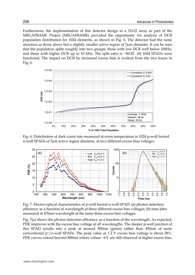
Furthermore, the implementation of this detector design in a 32x32 array as part of the MEGAFRAME Project (MEGAFRAME) provided the opportunity for analysis of DCR population distribution for 1024 elements, as shown in Fig. 6. The detector had the same
structure as those above but a slightly smaller active region of 7μm diameter. It can be seen that the population splits roughly into two groups: those with low DCR well below 100Hz, and those with higher DCR up to 10 kHz. The split ratio is ~80:20. All 1024 SPADs were functional. The impact on DCR by increased excess bias is evident from the two traces in Fig. 6.
1.E+00
1.E+01
1.E+02
1.E+03
1.E+04
1.E+05
0% 10% 20% 30% 40% 50% 60% 70% 80% 90% 100%
% of 1024 Total Population
DC
R (
Hz)
Cumulative % 0.65V
Cumulative % 0.8V
Average: 1.1KHz
Median: 26 Hz
Mode: 20 Hz
Fig. 6. Distribution of dark count rate measured at room temperature in 1024 p-well buried
n-well SPADs of 7μm active region diameter, at two different excess bias voltages.
1
10
100
1000
-1.0
Time (ns)
Co
un
ts
-0.8
-0.6
-0.4
-0.2
0.0
0.2
0.4
0.6
0.8
1.0
(b)Low Vex=0.4 V
Mid Vex=0.8 V
High Vex=1.2 V
0
5
10
15
20
25
30
300 400 500 600 700 800 900 1000 1100
Wavelength (nm)
PD
E (
%)
Low Vex=0.4 V
Mid Vex=0.8 V
High Vex=1.2 V
(a)
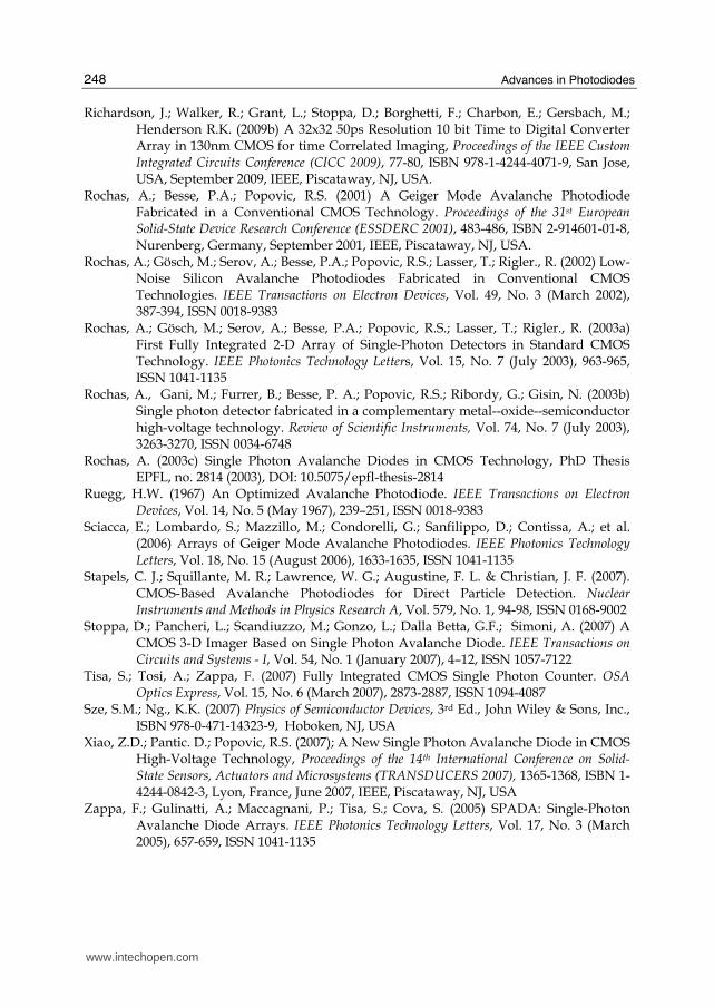
Fig. 7. Electro-optical characteristics of p-well buried n-well SPAD: (a) photon detection efficiency as a function of wavelength at three different excess bias voltages; (b) time jitter measured at 470nm wavelength at the same three excess bias voltages.
Fig. 7(a) shows the photon detection efficiency as a function of the wavelength. As expected, PDE improves with the excess bias voltage at all wavelengths. The deeper p-well junction of this SPAD results into a peak at around 500nm (green) rather than 450nm of more conventional p+/n-well SPADs. The peak value at 1.2 V excess bias voltage is about 28%. PDE curves extend beyond 800nm where values ~6% are still observed at higher excess bias.
www.intechopen.com

Avalanche Photodiodes in Submicron CMOS Technologies for High-Sensitivity Imaging
239
The increased response in the near infra-red is useful for several applications, among them time-of-flight 3D range sensing applications. The perturbations in the response are due to constructive/destructive interference patterns caused by the dielectric stack above the detector, which consists of several different materials with varying refractive indices. Fig. 7(b) shows the timing histograms measured at 470nm wavelength and at the same excess bias voltages as in Fig. 7(a). Timing resolution is measured as the FWHM of the distributions. Its values are 199 ps, 192 ps, and 184 ps, at low, mid, and high excess bias voltage, respectively. A distinct, exponential tail extends for around 1ns after the peak, evidence of a diffusion related timing delay. Table 3 shows a performance comparison for SPADs fabricated in 130nm CMOS technologies. As can be seen, a dramatic improvement in DCR can be achieved by adopting proper implant layers which lower the electric field, at the expense of a degradation in the jitter, that however remains good enough for most applications.
Reference This work Gersbach 2009 Niclass 2007
Active area 50.3 μm2 58 μm2 53 μm2
Type p+/p-well/buried n-well p+/n-well p+/n-well
Guard ring buried n-well with poly gate
STI with p-type passivation
p-well/STI with poly gate
VBD 14.3V 9.4V 9.7V
DCR 40Hz@Vex=1V 670kHz@Vex=2V 100kHz@Vex=1.7V
PDE 28%@ 500nm 30%@480nm 34%@450nm
Jitter 184ps FWHM 125ps FWHM 144 ps FWHM
Afterpulsing 0.02%@TD=100ns <1%@TD=180ns n.a.
Table 3. Performance comparison of SPADs made in 130nm CMOS technologies.
5.2 Linear-mode APD In order to implement APD-based pixels with integrated low-voltage readout channels, both terminals of the photodiode must be available: one to apply a high voltage and the other to connect the readout channel. This restricts the choice of the structure to the p+/n-well type (although also n+/floating p-well would be feasible). With technology scaling, the well doping levels are steadily increasing to allow the integration of smaller-size MOSFETs. Therefore, APDs fabricated in standard wells would have decreasing breakdown voltages and increasing tunneling dark currents when migrating the design to more advanced technology nodes. However, in High Voltage processes, a larger choice of layers with different doping levels are available, and can be exploited in the realization of APDs, both to obtain an efficient guard ring and a suitable doping for the multiplication region. The High Voltage option can then enable the fabrication of APDs also in deep sub-micron technologies. One key aspect to understand is how the noise factor scales with technology. Unfortunately, there are only a few examples of noise-characterized CMOS APDs in the literature, so that only some basic guidelines can be drawn. Fig. 8 shows the measured noise factor for two p+/n-well APDs fabricated in two different
technologies. The APD in Fig.8(a), fabricated in a 0.7μm High Voltage technology, has a breakdown voltage of 20.8V, and exhibits a low noise factor at low wavelengths because of electron-initiated avalanche. At higher wavelengths, however, noise increases considerably due to the hole-initiated avalanche noise. The measurements are in good agreement with
www.intechopen.com

Advances in Photodiodes
240
McIntyre noise theory, considering an ionization ratio k=0.2. The device of Fig. 8(b),
fabricated in 0.35μm CMOS technology, exhibits low noise also in the case of hole-initiated avalanche. The measured noise does not correspond to the one predicted by McIntyre theory because of the dead-space effect. This device is therefore more suitable for imaging applications in the visible spectral region. A further improvement in the noise factor could be given by n+ on floating p-well, which would combine the low noise of electron initiated avalanche with the requirement to access both device terminals. However, for this device structure, there is no experimental noise characterization available so far.
0
10
20
30
40
50
60
0 10 20 30 40
No
ise
fa
cto
r, F
Multiplication gain, M
Exp. 650nm
Exp. 380nm
Theory holes
Theory electrons
0
5
10
15
20
25
30
0 10 20 30 40 50
No
ise
fa
cto
r, F
Multiplication gain, M
Exp. 560nm
Exp. 380nm
Theory holes
Theory electrons
(a) (b)
Fig. 8. Noise factor as a function of multiplication gain at two illumination wavelengths in
two APDs made from: (a) 0.7μm High Voltage and (b) 0.35μm standard CMOS technology.
0.1
1
10
1 10 100
Ga
in n
on
um
ifo
rmit
y, σ M
[%]
Multiplication Gain, M
Different dies
Same die
Fig. 9. Gain uniformity between 0.35μm CMOS APDs fabricated on the same die and on different dies in the same production batch.
In the implementation of avalanche photodiode arrays, an important factor to take into account is gain uniformity. As multiplication gain increases, the voltage range allowing a tolerable gain variation progressively reduces. Therefore, if small non-uniformities between different APDs can be corrected via pixel-by-pixel calibration, large non-uniformities are detrimental to the correct operation of the array. In order to evaluate the uniformity of APDs made on the same die, a small set of identical APDs, whose characteristics were reported in
www.intechopen.com

Avalanche Photodiodes in Submicron CMOS Technologies for High-Sensitivity Imaging
241
(Pancheri et al., 2008), were fabricated in a 0.35μm CMOS technology. For every APD in the die and for several dies, the gain was measured as a function of voltage. Gain non-uniformity, expressed as standard deviation, is reported as a function of average gain in Fig. 9. It can be observed that the gain non-uniformity of APDs fabricated on different dies (in the same production batch) is 10 times higher than the non-uniformity of gains for APDs belonging to the same die. In this last case, a non-uniformity better than 1% is achieved for a gain M=40. This demonstrates the feasibility of linear-mode APD arrays in that specific technology.
6. Integrated read-out channels for SPADs
Two basic circuit elements are required to read-out a SPAD: i) a quench circuit to detect and
stop the avalanche event, followed by restoration of bias conditions; ii) a buffer to isolate the
SPAD from the capacitance of external processing electronics. The integration of more
complex processing and support circuits such as time-to-digital conversion, gated ripple
counters and charge pumps is the subject of much recent research (Niclass et al., 2008;
Richardson et al., 2009b; Guerrieri et al., 2010). However, as the main properties of the
optical system are set by the choice of quench circuit and associated biasing arrangement for
the SPAD we will focus on these aspects in more detail. (a) SPAD Orientation Options Since a SPAD is a two terminal diode, operated at an excess bias potential beyond its
breakdown voltage, it may be oriented in two ways; either with a negative potential on the
anode, or positive on the cathode. As previously discussed, it is desirable to minimise
detector dead time and charge flow quantity during an avalanche event. The optimal
connectivity to permit this depends on the parasitic capacitances which are specific to the
diode construction which has been implemented.
To illustrate this point, two possible passive quench configurations are shown in Fig. 10 for
a SPAD implemented within a deep n-well, p-substrate technology such as that of
(Pauchard et al., 2000b ) Fig. 10(a) shows a large negative voltage applied to the anode, with
a much smaller positive excess bias applied via the passive quench PMOS to the cathode.
Fig. 10(b) employs an NMOS quench component with source connected to ground potential,
and a large positive bias potential Vbias_total applied to the SPAD cathode. In both cases the
key moving ‘sense’ node of the circuit is at the buffer/comparator input terminal. The time
domain output signal is determined by the threshold voltage of the buffer, the SPAD excess
bias voltage and recharge time constant.
In configuration (a) the cathode is the moving node and therefore the additional capacitance
of the n-well to p-substrate parasitic diode (Cnwell) must also be charged and discharged
during the detector operating cycle. As well as contributing to the lengthening of detector
dead time due to the increased RC load, this adds to the volume of charge flow through the
detector, so increasing probability of afterpulsing. Configuration (a) also places a limitation
on the maximum negative Vbreakdown that can be applied without forward biasing the n-well
p-substrate junction. The maximum voltage Vex that can be applied is determined by the
transistor gate-oxide breakdown voltages, typically 3.3V for thick oxide devices. Thus
voltages beyond Vbreakdown + Vex + Vdiode across the SPAD will induce a latch-up behaviour
where the buffer input voltage will transit below –Vdiode drawing current from the substrate
ground potential through the forward biased parasitic diode.
www.intechopen.com

Advances in Photodiodes
242
Vex
-Vbreakdown
MquenchVquench
Vout
Vbias_total
MquenchVquench
Vout Vth
Cpn
Cpn
Cnwell
(a)
Dnwell
Cnwell
Dnwell
(b)
Fig. 10. SPADs biased with (a) PMOS quench (b) NMOS quench
In the case of the ‘flipped’ configuration (b) the anode of the detector is the moving node, and therefore there is only the charging of the SPAD junction capacitance to consider. Importantly, this permits the sharing of n-well regions by multiple elements within an array implementation leading to reduced pixel pitches and improved fill factor. However, it should be noted that it is common for the mobility of an NMOS transistor channel to be higher than PMOS in deep submicron processes (the intrinsic conductivity Kp can be typically ¼ of Kn), which leads to a larger equivalent area used when compared to a PMOS implementation for the same target quench resistance. Configuration (b) will only operate correctly as a SPAD provided the voltage applied to the SPAD active region Vbias_total = Vbreakdown + Vex is lower than the breakdown voltage of the parasitic n-well/p-substrate or n-well/p-well peripheral diodes. Indeed the n-well of these parasitic diodes can act as the base of a parasitic bipolar transistor inducing a latch-up condition and so the resistivity of the buried n-well is of concern. Regardless of orientation, for reliability reasons it is vital not to exceed the maximum gate oxide potential of the output buffer otherwise permanent damage can occur. For this reason it is common to employ thick gate oxide transistors for this circuit if available in the target technology. A clamping diode may be used in configuration (b) to ensure safe operating region of the buffer transistors are respected. Both orientations are prevalent in the published literature, for example (Ghioni et al, 1996)
implementing configuration (b), and (Pancheri & Stoppa, 2007), and (Niclass, 2008). Yet
more bias options are shown in Fig.11(a) and (b) where the SPAD is capacitively coupled to
the output buffer and quenched by a passive resistor. The resistors can be conveniently
made from high ohmic polysilicon and the capacitors by metal-metal finger (MOM)
capacitors paying attention to the dielectric reliability at the high voltages. Such circuits
decouple the d.c. bias conditions of the SPAD from those at the input of the digital buffer
(fixed by Mkeep). Only the pulse of the SPAD is transferred to the output. The capacitor Cls
must be chosen such that capacitive division by the input capacitance of the buffer does not
attenuate the SPAD pulse below the minimum required by the buffer trigger threshold. In
practice, Cls can easily be as small as a few femto Farads. The circuit of Fig. 11(a) allows the
p-well of the SPAD to be biased at ground potential (in common with all NMOS p-wells).
The circuit of Fig. 11(b) allows the moving node of the SPAD to be the lower capacitance p-
well while the n-well is biased at a low voltage avoiding breakdown issues with n-well/p-
substrate junctions. These floating circuits also permit a differential bias arrangement
www.intechopen.com

Avalanche Photodiodes in Submicron CMOS Technologies for High-Sensitivity Imaging
243
whereby Vbias_pos and Vbias_neg are set to +Vbias_total/2 and –Vbias_total/2 respectively. This
minimises the stress on the parasitic wells and eases power supply generation.
Vbias_pos
Vbias_neg
Vout
Mkeep
Cpn
Cnwell
(a)
Dnwell
Vdd
Cls
Vbias_pos
Vbias_neg
Vout Mkeep
Cpn
Cnwell
Dnwell Vdd Cls
Rq
Rq
(b)
Fig. 11. Floating SPAD orientation options.
(b) Quench Resistor Optimisation Incorrectly sized passive quench circuitry can result in undesirable circuit operation, such as lengthy and inconsistent dead times. This introduces noise, imposes severe dynamic range limitations, particularly impacting photon counting applications and those employing gated counters such as ranging, 3D cameras and fluorescence lifetime imaging microscopy (FLIM). The p-well to buried n-well diode and parasitic n-well to p-substrate diodes are often modelled in foundry technology information allowing extraction of junction capacitance. Parasitic capacitive elements of the quench circuit can be predicted using layout-vs-schematics (LVS) extraction tools. This means that the passive quench MOS element can be sized appropriately for linear mode operation, and accurate simulations performed.
Vex
-Vbreakdown
MquenchVquench
Vout
CpnCnwell
τ1 τ2
linear
sat
Vth
(a) (b)
VSPAD
Fig. 12. Passive Quench Optimisation
This optimisation process is illustrated in Fig. 12. Fig. 12(a) shows the basic passive quench circuit, parasitic elements and waveforms. Fig. 12(b) shows how noise can cause increased dead time variation in a non-optimised system. In an optimised configuration the crossing of the inverter threshold (Vth) is performed at a steep gradient. Noise on the moving node
results in variation of dead time τ1 at the inverter output. If the passive quench element W/L ratio is too small, the extended RC recharge time degrades noise immunity and results
in a higher dead time variation τ2. In the most basic configuration the gate of the PMOS passive quench element is simply grounded. Under the aforementioned non-optimal circumstances a small negative voltage can be applied to the gate of the PMOS transistor but
www.intechopen.com

Advances in Photodiodes
244
this is considered an undesirable complication. Similarly, in the case of an undersized PMOS element, a positive voltage must be applied to its gate to ensure an output pulse is generated. In a low voltage process, with comparatively low overall excess bias conditions, for the bulk of the quenching and reset cycle the PMOS element is mainly operating in linear mode, with a brief entry into saturation (see Fig. 12(b)). Thus, equations (1), (2), and (3) can be applied to optimise the passive quench element aspect ratio:
1 quench tot
tR C
SPAD exV V e⋅⎛ ⎞= −⎜ ⎟⎜ ⎟⎝ ⎠ (1)
/(2 )quench ex MquenchR V Id= ⋅ (2)
( )2ds
Mquench p gs t ds
VWId K V V V
L
⎡ ⎤= − − ⋅⎢ ⎥⎣ ⎦ (3)
For a parasitic capacitance Ctot = 50fF, Vex=1.2V and inverter threshold Vth=0.6V, for a dead
time of 20ns and a PMOS passive quench element with Kp= 30 μA/V2, equations yield:
Rquench≈400kΩ, Id=0.6μA, and (W/L)=1/8. Therefore for a 0.35μm width, grounded gate
PMOS transistor, length L should be ~2.7μm to meet the above specification.
7. Conclusion
We have reported on CMOS avalanche photodiodes, reviewing the most significant devices so far proposed in the literature and discussing selected results from our research activities and relevant to both Geiger-mode and linear-mode APDs. In spite of the technological constraints and design rule restrictions in advanced manufacturing processes, smart design solutions for SPADs and the read-out electronics exist that allow very for good performance even in the 130nm CMOS technological node, thus paving the way to new application fields for high resolution, SPAD based image sensors. As far as linear-mode CMOS APD are concerned, although these devices have not been developed to the same extent as SPADs, our results demonstrate that acceptable excess noise figures can be achieved at moderate gain even at relatively large wavelengths. Moreover, the spatial uniformity of the gain is found to be reasonably good in devices from the same die, so that the design of APD based pixel arrays for high-sensitivity imaging can be envisioned.
8. References
APD producers: Advanced Photonix (www.advancedphotonix.com), EG&G (www.urscorp.com), Hamamatsu Photonics (www.hamamatsu.com), Perkin Elmer (www.PerkinElmer.com), RMD (www.rmdinc.com)
Aull, B.F.; Loomis, A.H.; Young, D.J.; Heinrichs, R.M.; Felton, B.J.; Daniels, P.J., Landers, D.J. (2002) Geiger-Mode Avalanche Photodiodes for Three-Dimensional Imaging. Lincoln Laboratory Journal, Vol. 13, No. 2 (2002), 335-350, ISSN 0896-4130
Biber, A.; Seitz, P. & Jäckel, H. (2001). Avalanche Photodiode Image Sensor in Standard Silicon BiCMOS Technology. Sensors and Actuators A: Physical, Vol. 90, No. 1-2 (May 2001), 82-88, ISSN 0924-4247
www.intechopen.com

Avalanche Photodiodes in Submicron CMOS Technologies for High-Sensitivity Imaging
245
Cova, S.; Longoni, A.; Andreoni, A. (1981) Toward Picosecond Resolution with Single-Photon Avalanche Diodes, Review of Scientific Instruments, Vol. 52, No. 3 (March 1981), 408-412, ISSN 0034-6748
Cova, S.; Ghioni, M.; Lacaita, A.; Samori, C.; Zappa, F. (1996) Avalanche Photodiodes and Quenching Circuits For Single-Photon Detection. Applied Optics, Vol. 35, No. 12 (April 1996), 1956-1976, ISSN 1943-8206
Cova, S.; Ghioni, M.; Lotito, A.; Rech, I.; Zappa, F. (2004) Evolution and Prospects for Single-Photon Avalanche Diodes and Quenching Circuits. Journal of Modern Optics, Vol. 51, No. 9-10 (June-July 2004), 1267-1288, ISSN 0950-0340
Dussault, D.; Hoess, P. (2004) Noise Performance Comparison of ICCD with CCD and EMCCD Cameras, Proceedings of SPIE, Vol. 5563, 195-204, ISBN 0-8194-5501-6, Denver, August 2004, SPIE, Bellingham, WA, USA
Faramarzpour, N.; Deen, M.j.; Shirani, S.; Fang, Q. (2008) Fully Integrated Single Photon
Avalanche Diode Detector in Standard CMOS 0.18μm Technology. IEEE Transactions on Electron Devices, Vol. 55, No. 3 (March 2008), 760–767, ISSN 0018-9383
Finkelstein, H.; Hsu, M.J.; Esener, S.C. (2006a) An Ultrafast Geiger-Mode Single-Photon
Avalanche Diode in a 0.18μm CMOS Technology. Proceedings of SPIE, Vol. 6372, 63720W.1-63720W.10, ISBN 0-8194-6470-8, Boston, USA, Oct 2006, SPIE, Bellingham, WA, USA
Finkelstein, H.; Hsu, M.J.; Esener, S.C. (2006b) STI-Bounded Single-Photon Avalanche Diode in a Deep-Submicrometer CMOS Technology, IEEE Electron Device Letters, Vol. 27, No. 11 (November 2006), 887-889, ISSN 0741-3106
Gersbach, M. ; Niclass, C.; Charbon, E.; Richardson, J.; Henderson, R.; Grant, L. (2008) A Single Photon Detector Implemented in a 130nm CMOS Imaging Process, Proceedings of the 38th European Solid-State Device Research Conference (ESSDERC 2008), pp. 270-273, ISBN 978-1-4244-2363-7, Edinburgh (UK), September 2008, IEEE, Piscataway, NJ, USA
Gersbach, M. ; Richardson, J.; Mazaleyrat, E.; Hardillier, S.; Niclass, C.; Henderson, R.; Grant, L. Charbon, E. (2009) A Low-Noise Single-Photon Detector Implemented in a 130nm CMOS Imaging Process, , Solid-State Electronics, Vol. 53, No. 7 (July 2009), 803-808, ISSN 0038-1101
Ghioni, M.; Cova, S.; Lacaita, A.; Ripamonti, G. (1988) New Silicon Epitaxial Avalanche Diode for Single-Photon Timing at Room Temperature. Electronics Letters, Vol. 24, No. 4 (November 1988), 1476-1477, ISSN 0013-5194
Ghioni, M.; Cova, S.; Zappa, F.; Samori, C. (1996) Compact Active Quenching Circuit for Fast Photon Counting with Avalanche Photodiodes. Review of Scientific Instruments, Vol. 67, No. 10 (October 1996), 3440-3448, ISSN 0034-6748
Ghioni, M.; Gulinatti, A.; Rech, I.; Zappa, F.; Cova, S. (2007) Progress in Silicon Single-Photon Avalanche Diodes. IEEE Journal of Selected Topics in Quantum Electronics, Vol. 13, No. 4 (July/August 2007), 852-862, ISSN 1077-260X
Goetzberger, A.; Mc Donald, B.; Haitz, R.H., Scarlett, R. M. (1963) Avalanche Effects in Silicon p---n Junctions. II. Structurally Perfect Junctions. Journal of Applied Physics, Vol. 34, No. 6 (June 1963), 1591-1600, ISSN 0021-8979
www.intechopen.com

Advances in Photodiodes
246
Guerrieri, F.; Tisa, S.; Tosi, A.; Zappa, F. (2010); Single-Photon Camera for High-Sensitivity High-Speed Applications, Proceedings of SPIE, Vol. 7536, 753605.1-753605.10, ISBN 0-8194-7929-2, San Jose, USA, January 2010, SPIE, Bellingham, WA, USA
Haitz, R.H., Goetzberger, A.; Scarlett, R. M. ; Shockley, W. (1963) Avalanche Effects in Silicon p---n Junctions. I. Localized Photomultiplication Studies on Microplasmas. Journal of Applied Physics, Vol. 34, No. 6 (June 1963), 1581-1590, ISSN 0021-8979
Haitz, R.H. (1964) Model for the Electrical Behavior of a Microplasma. Journal of Applied Physics, Vol. 35, No. 5 (May 1964), 1370-1376, ISSN 0021-8979
Haitz, R.H. (1965) Mechanisms Contributing to the Noise Pulse Rate of Avalanche Diodes. Journal of Applied Physics, Vol. 36, No. 10 (October 1965), 3123-3131, ISSN 0021-8979
Hayat, M. M.; Sargeant, W. L. & Saleh, B. E. A. (1992). Effect of Dead Space on Gain and Noise in Si and GaAs Avalanche Photodiodes. IEEE Journal of Quantum Electronics, Vol. 28, No. 5 (May 1992), 1360 – 1365, ISSN 0018-9197
Huang, W.-K.; Liu, Y.-C. & Hsin, Y.-M. (2007). A High-Speed and High-Responsivity Photodiode in Standard CMOS Technology. IEEE Photonics Technology Letters, Vol. 19, No. 4 (February 2007), 197 – 199, ISSN 1041-1135
Hsu, M.J.; Esener, S.C.; Finkelstein, H. (2009) A CMOS STI-Bounded Single-Photon Avalanche Diode with 27-ps Timing Resolution and a Reduced Diffusion Tail, IEEE Electron Device Letters, Vol. 30, No. 6 (June 2009), 641-643, ISSN 0741-3106
Iiyama, K.; Takamatsu, H. & Maruyama, T. (2009). Silicon Lateral Avalanche Photodiodes Fabricated by Standard 0.18 μm CMOS Process. Proceedings of the 35th European Conference on Optical Communication (ECOC ’09), P2.06, ISBN 978-1-4244-5096-1, Vienna, Austria, September 2009, VDE VERLAG GMBH, Berlin, Germany
Kang, H.-S.; Lee, M.-J. & Choi, W.-Y. (2007). Si Avalanche Photodetectors Fabricated in Standard Complementary Metal-Oxide-Semiconductor Process. Applied Physics Letters, Vol. 90, No. 15 (April 2007), 151118, ISSN 0003-6951
Kim, Y. S.; Jun, I. S. & Kim, K. H. (2008). Design and Characterization of CMOS Avalanche Photodiode With Charge Sensitive Preamplifier. IEEE Transactions on Nuclear Science, Vol. 55, No. 3 (June 2008), 1376-1380, ISSN 0018-9499
Kindt, W.J. (1994) A Novel Avalanche Photodiode Array, Conference Record of the IEEE Nuclear Science Symposium (NSS 1994), pp. 164-167, ISBN 0-7803-2544-3, Norfolk (USA), October/November 1994, IEEE, Piscataway, NJ, USA
Lacaita, A. ; Ghioni, M.; Cova, S. (1989) Double Epitaxy Improves Single-Photon Avalanche Diode Performance. Electronics Letters, Vol. 25, No. 13 (June 1989), 841–843, ISSN 0013-5194
Lacaita, A. ; Zappa, F.; Bigliardi, S.; Manfredi, M. (1993a) On the Bremsstrahlung Origin of Hot-Carrier-Induced Photons in Silicon Devices. IEEE Transactions on Electron Devices, Vol. 40, No. 3 (March 1993), 577–582, ISSN 0018-9383
Lacaita, A. ; Zappa, F.; Bigliardi, S.; Manfredi, M. (1993b) Single-Photon Avalanche Diode with Ultrafast Pulse Response Free from Slow Tails. IEEE Electron Device Letters, Vol. 14, No. 7 (July 1993), 360-362, ISSN 0741-3106
Marwick, M.A.; Andreou, A.G. (2008) Single Photon Avalanche Photodetector with
Integrated Quenching Fabricated in TSMC 0.18 μm 1.8 V CMOS process. Electronics Letters, Vol. 44, No. 10 (May 2008), 643-644, ISSN 0013-5194
McIntyre, R.J. (1961) Theory of Microplasma Instability in Silicon. Journal of Applied Physics, Vol. 32, No. 6 (June 1961), 983-995, ISSN 0021-8979
www.intechopen.com

Avalanche Photodiodes in Submicron CMOS Technologies for High-Sensitivity Imaging
247
McIntyre, R.J. (1966) Multiplication Noise in Uniform Avalanche Diodes. IEEE Transactions on Electron Devices, Vol. 13, No. 1 (January 1966), 164–168, ISSN 0018-9383
MEGAFRAME: Million Frame Per Second, Time-Correlated Single Photon Camera, IST FP6 FET Open Project 029217, http://www.megaframe.eu
Niclass, C.; M. Sergio, M.; Charbon, E. (2006) A Single Photon Avalanche Diode Array
Fabricated in 0.35μm CMOS and Based on an Event Driven Readout for TCSPC Experiments. Proceedings of SPIE, Vol. 6372, 63720S.1-63720S.12, ISBN 0-8194-6470-8, Boston, USA, Oct 2006, SPIE, Bellingham, WA, USA
Niclass, C.; Gersbach, M.; Henderson, R.; Grant, L.; Charbon, E. (2007) A Single Photon Avalanche Diode implemented in 130-nm CMOS Technology. IEEE Journal on Selected Topics in Quantum Electronics, Vol. 13, No. 4 (July/August 2007), 863-869, ISSN 1067-260X
Niclass, C. (2008) Single-Photon Image Sensors in CMOS : Picosecond Resolution for Three-Dimensional Imaging, PhD Thesis EPFL, no. 4161 (2008), DOI: 10.5075/epfl-thesis-4161
Pancheri, L. & Stoppa, D. (2007) Low-Noise CMOS Single-Photon Avalanche Diodes with 32 ns Dead Time. Proceedings of the 37th European Solid-State Device Research Conference (ESSDERC 2007), 362-365, ISBN 978-1-4244-1123-8, Muenchen, Germany, September 2007, IEEE, Piscataway, NJ, USA
Pancheri, L.; Scandiuzzo, M.; Stoppa, D; Dalla Betta, G.-F. (2008). Low-Noise Avalanche Photodiode in Standard 0.35-μm CMOS Technology. IEEE Transactions on Electron Devices, Vol. 55, No. 1 (January 2008), 457-461, ISSN 0018-9383
Pancheri, L. & Stoppa, D. (2009). A SPAD-based Pixel Linear Array for High-Speed Time-Gated Fluorescence Lifetime Imaging. Proceedings of the European Solid-State Circuits Conference (ESSCIRC 2009), 428-431, ISBN 978-1-4244-4354-3, Athens, Greece, September 2009, ERGO Publications, Athens, Greece
Pauchard, A.; Rochas, A.; Ranjelovic, Z.; Besse, P.A.; Popovic, R.S. (2000a) Ultraviolet Avalanche Photodiode in CMOS Technology, Technical Digest of the IEEE International Electron Device Meeting (IEDM 2000), 30.6.1-30.6.4, ISBN 0-7803-6438-4, San Francisco (USA), December 2000, IEEE, Piscataway NJ, USA.
Pauchard, A.; Besse, P.A.; Martek, M.; Wolffenbuttel, R.F.; Popovic, R.S. (2000b) Ultraviolet-Selective Avalanche Photodiode. Sensors and Actuators A: Physical, Vol. 82, No. 1-3 (May 2000), 128-134, ISSN 0924-4247
Petrillo, G.A.; McIntyre, R. J.; Lecomte, R.; Lamoureux, G.; Schmitt, D. (1984) Scintillation Detection with Large-Area Reach-Through Avalanche Photodiodes. IEEE Transactions on Nuclear Science, Vol. 31, No. 1 (January 1984), 417–423, ISSN 0018-9499
Renker, D. (2004) Photosensors. Nuclear Instruments and Methods in Physics Research A, Vol. 527, No. 1-2, (July 2004), 15-20, ISSN 0168-9002
Renker, D. (2006) Geiger-Mode Avalanche Photodiodes, History, Properties and Problems. Nuclear Instruments and Methods in Physics Research A, Vol. 567, No. 1 (November 2006), 48-56, ISSN 0168-9002
Richardson, J.A.; Grant, L.A.; Henderson, R.K. (2009a) Low Dark Count Single-Photon Avalanche Diode Structure Compatible with Standard Nanometer Scale CMOS Technology. IEEE Photonics Technology Letters, Vol. 21, No. 14 (July 2009), 1020-1022, ISSN 1041-1135
www.intechopen.com
Advances in Photodiodes
248
Richardson, J.; Walker, R.; Grant, L.; Stoppa, D.; Borghetti, F.; Charbon, E.; Gersbach, M.; Henderson R.K. (2009b) A 32x32 50ps Resolution 10 bit Time to Digital Converter Array in 130nm CMOS for time Correlated Imaging, Proceedings of the IEEE Custom Integrated Circuits Conference (CICC 2009), 77-80, ISBN 978-1-4244-4071-9, San Jose, USA, September 2009, IEEE, Piscataway, NJ, USA.
Rochas, A.; Besse, P.A.; Popovic, R.S. (2001) A Geiger Mode Avalanche Photodiode Fabricated in a Conventional CMOS Technology. Proceedings of the 31st European Solid-State Device Research Conference (ESSDERC 2001), 483-486, ISBN 2-914601-01-8, Nurenberg, Germany, September 2001, IEEE, Piscataway, NJ, USA.
Rochas, A.; Gösch, M.; Serov, A.; Besse, P.A.; Popovic, R.S.; Lasser, T.; Rigler., R. (2002) Low-Noise Silicon Avalanche Photodiodes Fabricated in Conventional CMOS Technologies. IEEE Transactions on Electron Devices, Vol. 49, No. 3 (March 2002), 387-394, ISSN 0018-9383
Rochas, A.; Gösch, M.; Serov, A.; Besse, P.A.; Popovic, R.S.; Lasser, T.; Rigler., R. (2003a) First Fully Integrated 2-D Array of Single-Photon Detectors in Standard CMOS Technology. IEEE Photonics Technology Letters, Vol. 15, No. 7 (July 2003), 963-965, ISSN 1041-1135
Rochas, A., Gani, M.; Furrer, B.; Besse, P. A.; Popovic, R.S.; Ribordy, G.; Gisin, N. (2003b) Single photon detector fabricated in a complementary metal--oxide--semiconductor high-voltage technology. Review of Scientific Instruments, Vol. 74, No. 7 (July 2003), 3263-3270, ISSN 0034-6748
Rochas, A. (2003c) Single Photon Avalanche Diodes in CMOS Technology, PhD Thesis EPFL, no. 2814 (2003), DOI: 10.5075/epfl-thesis-2814
Ruegg, H.W. (1967) An Optimized Avalanche Photodiode. IEEE Transactions on Electron Devices, Vol. 14, No. 5 (May 1967), 239–251, ISSN 0018-9383
Sciacca, E.; Lombardo, S.; Mazzillo, M.; Condorelli, G.; Sanfilippo, D.; Contissa, A.; et al. (2006) Arrays of Geiger Mode Avalanche Photodiodes. IEEE Photonics Technology Letters, Vol. 18, No. 15 (August 2006), 1633-1635, ISSN 1041-1135
Stapels, C. J.; Squillante, M. R.; Lawrence, W. G.; Augustine, F. L. & Christian, J. F. (2007). CMOS-Based Avalanche Photodiodes for Direct Particle Detection. Nuclear Instruments and Methods in Physics Research A, Vol. 579, No. 1, 94-98, ISSN 0168-9002
Stoppa, D.; Pancheri, L.; Scandiuzzo, M.; Gonzo, L.; Dalla Betta, G.F.; Simoni, A. (2007) A CMOS 3-D Imager Based on Single Photon Avalanche Diode. IEEE Transactions on Circuits and Systems - I, Vol. 54, No. 1 (January 2007), 4–12, ISSN 1057-7122
Tisa, S.; Tosi, A.; Zappa, F. (2007) Fully Integrated CMOS Single Photon Counter. OSA Optics Express, Vol. 15, No. 6 (March 2007), 2873-2887, ISSN 1094-4087
Sze, S.M.; Ng., K.K. (2007) Physics of Semiconductor Devices, 3rd Ed., John Wiley & Sons, Inc., ISBN 978-0-471-14323-9, Hoboken, NJ, USA
Xiao, Z.D.; Pantic. D.; Popovic, R.S. (2007); A New Single Photon Avalanche Diode in CMOS High-Voltage Technology, Proceedings of the 14th International Conference on Solid-State Sensors, Actuators and Microsystems (TRANSDUCERS 2007), 1365-1368, ISBN 1-4244-0842-3, Lyon, France, June 2007, IEEE, Piscataway, NJ, USA
Zappa, F.; Gulinatti, A.; Maccagnani, P.; Tisa, S.; Cova, S. (2005) SPADA: Single-Photon Avalanche Diode Arrays. IEEE Photonics Technology Letters, Vol. 17, No. 3 (March 2005), 657-659, ISSN 1041-1135
www.intechopen.com

Advances in PhotodiodesEdited by Prof. Gian Franco Dalla Betta
ISBN 978-953-307-163-3Hard cover, 466 pagesPublisher InTechPublished online 22, March, 2011Published in print edition March, 2011
InTech EuropeUniversity Campus STeP Ri Slavka Krautzeka 83/A 51000 Rijeka, Croatia Phone: +385 (51) 770 447 Fax: +385 (51) 686 166www.intechopen.com
InTech ChinaUnit 405, Office Block, Hotel Equatorial Shanghai No.65, Yan An Road (West), Shanghai, 200040, China
Phone: +86-21-62489820 Fax: +86-21-62489821
Photodiodes, the simplest but most versatile optoelectronic devices, are currently used in a variety ofapplications, including vision systems, optical interconnects, optical storage systems, photometry, particlephysics, medical imaging, etc. Advances in Photodiodes addresses the state-of-the-art, latest developmentsand new trends in the field, covering theoretical aspects, design and simulation issues, processing techniques,experimental results, and applications. Written by internationally renowned experts, with contributions fromuniversities, research institutes and industries, the book is a valuable reference tool for students, scientists,engineers, and researchers.
How to referenceIn order to correctly reference this scholarly work, feel free to copy and paste the following:
Gian-Franco Dalla Betta, Lucio Pancheri, David Stoppa, Robert Henderson and Justin Richardson (2011).Avalanche Photodiodes in Submicron CMOS Technologies for High-Sensitivity Imaging, Advances inPhotodiodes, Prof. Gian Franco Dalla Betta (Ed.), ISBN: 978-953-307-163-3, InTech, Available from:http://www.intechopen.com/books/advances-in-photodiodes/avalanche-photodiodes-in-submicron-cmos-technologies-for-high-sensitivity-imaging