avr atmega128 mikrokontroller - bme méréstechnika és ...szanto/mlab_eng/ml2_avr_m2_eng.pdf · 3...
TRANSCRIPT
AVR ATmega128
assembly

2
AVR assembly – directives
.include "m128def.inc"
– ATmega128 registers and bit specification file
.def temp = r16
– Register r16 renamed to temp
.equ tconst = 100
– Defining a constant value
.org $0046
– Set the memory address of the next instruction (in .cseg)
M_LOOP:
– Label (e.g. for jumps)
3
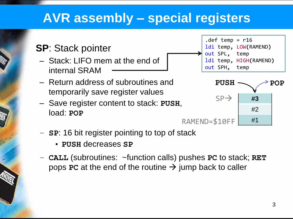
AVR assembly – special registers
SP: Stack pointer
– Stack: LIFO mem at the end of
internal SRAM
– Return address of subroutines and
temporarily save register values
– Save register content to stack: PUSH,
load: POP
– SP: 16 bit register pointing to top of stack
• PUSH decreases SP
#3
#2
#1 RAMEND=$10FF
SP
PUSH POP
– CALL (subroutines: ~function calls) pushes PC to stack; RET
pops PC at the end of the routine jump back to caller
.def temp = r16 ldi temp, LOW(RAMEND) out SPL, temp ldi temp, HIGH(RAMEND) out SPH, temp

Stack example
4
.org $0050 M_LOOP: ldi r16, 0x12 call STACKDEMO jmp M_LOOP STACKDEMO: push r16; r16=0x12
inc r16 ; r16=0x13
pop r16 ; r16=0x12
ret
$0050- $0051- $0053- $0055- $0056- $0057- $0058-
Instr. $10FC $10FD $10FE $10FF
Init ? ? ? ?
CALL ? ? 00 53
PUSH ? 12 00 53
POP ? 12 00 53
RET ? 12 00 53
SP

AVR assembly – special registers
Status register (SREG) – status flags
• I: global interrupt enable
• T: bit copy storage
• H: half-carry
• S: sign bit (N xor V)
• V: two’s complement overflow
• N: negative / result bit 7 (15)
• Z: zero flag / all bits 0
• C: carry flag 5

6
Software timing
6
• 11MHz millions of loops required vs. 1 byte counter 256
• Not for exact timing!
Multi-byte for loop
.def i = r16
.def j = r17 ; 300 = 0x12C
ldi i, HIGH(300)+1 ; =0x1+1
ldi j, LOW(300) ; =0x2C
LOOP: <instruction1>
dec j
brne LOOP
dec i
brne LOOP
<instruction2>
Z
Z
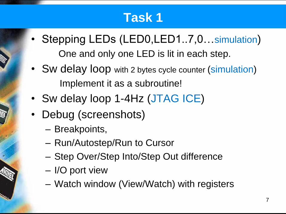
Task 1
• Stepping LEDs (LED0,LED1..7,0…simulation)
One and only one LED is lit in each step.
• Sw delay loop with 2 bytes cycle counter (simulation)
Implement it as a subroutine!
• Sw delay loop 1-4Hz (JTAG ICE)
• Debug (screenshots)
– Breakpoints,
– Run/Autostep/Run to Cursor
– Step Over/Step Into/Step Out difference
– I/O port view
– Watch window (View/Watch) with registers
7

Interrupt handling
8
Instruction
Instruction
Instruction
Disable global IT
Store PC
Load IT vector address to PC
Restore PC from stack
Enable global interrupt flag
Store main program’s context
to stack
Serve IT request
Instruction
Restore original context and
RETI
Done in hardware
Jump to IT handler
9
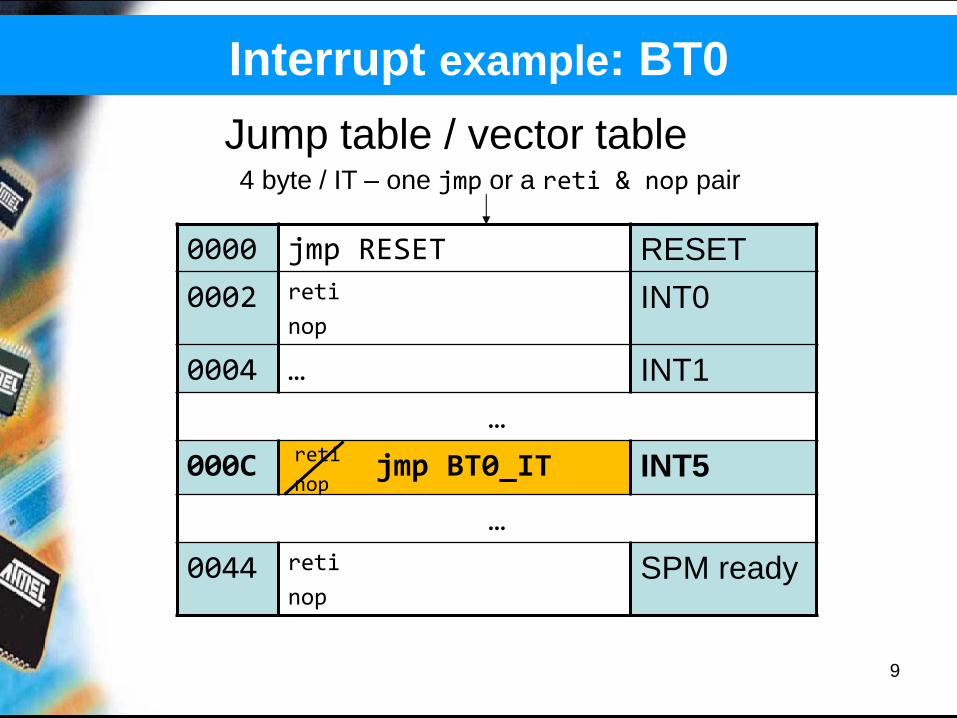
Jump table / vector table
Interrupt example: BT0
0000 jmp RESET RESET
0002 reti
nop INT0
0004 … INT1
…
000C jmp BT0_IT INT5
…
0044 reti
nop SPM ready
4 byte / IT – one jmp or a reti & nop pair
reti
nop

10
Interrupts on button press
Port E may be used as external interrupt source
– EICRB: control register – level or edge – EIMSK: enabled IT sources
– EIFR: flag register – „interrupt occurences”
port 7 6 5 4 3 2 1 0
E BT2 BT1 BT0 INT
;<set up PORT E as input, then..>
ldi temp, (1<<ISC51) ; INT5 falling edge
; same as 0b00001000
out EICRB, temp
ldi temp, (1<<INT5) ; enable INT5 interrupt
out EIMSK, temp
sei ; enable global IT
11
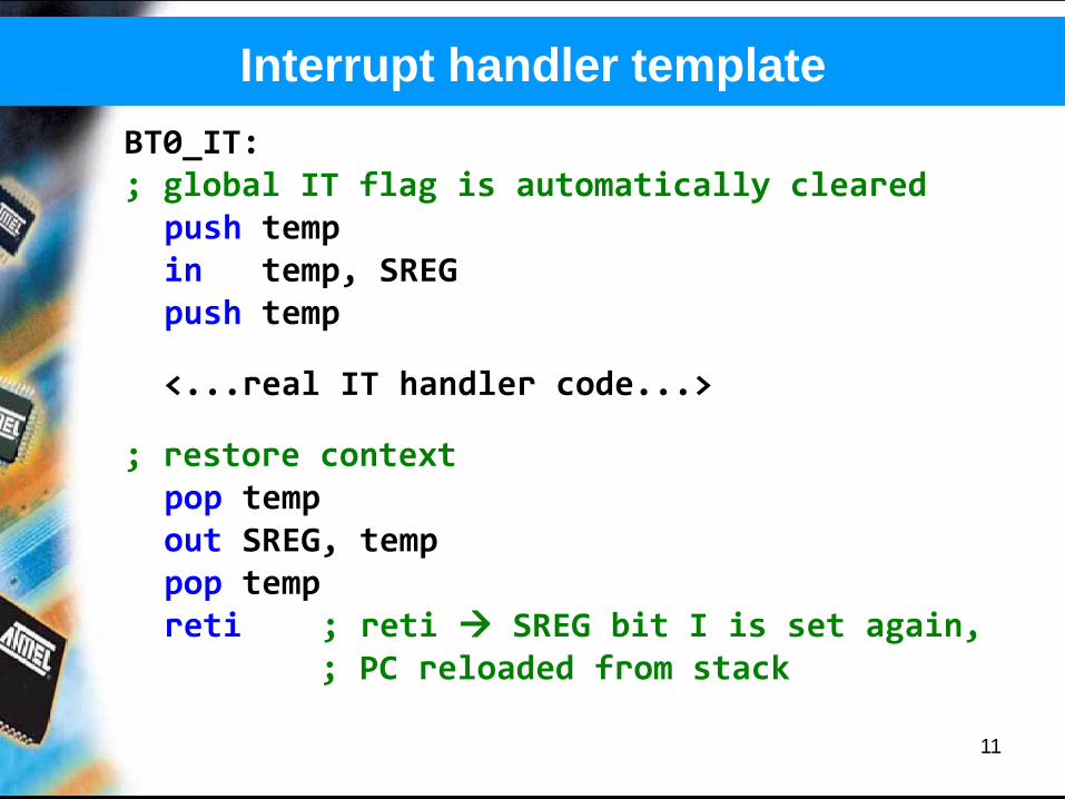
Interrupt handler template
BT0_IT: ; global IT flag is automatically cleared push temp in temp, SREG push temp
<...real IT handler code...>
; restore context pop temp out SREG, temp pop temp reti ; reti SREG bit I is set again, ; PC reloaded from stack
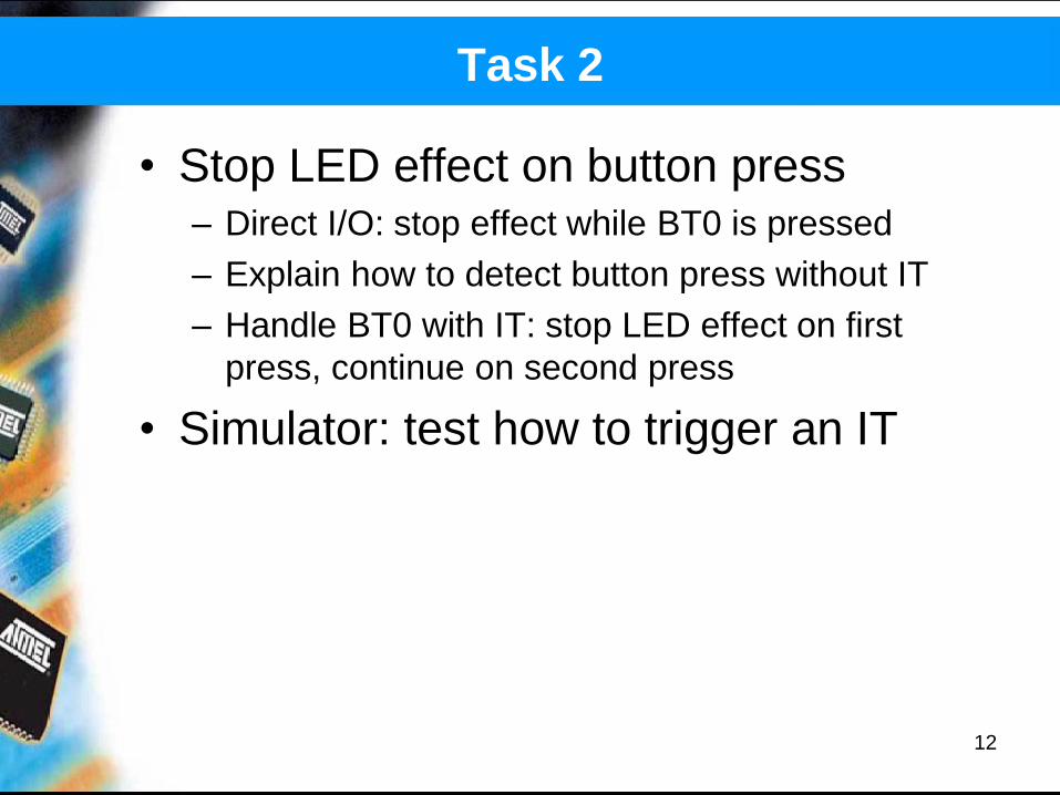
Task 2
• Stop LED effect on button press – Direct I/O: stop effect while BT0 is pressed
– Explain how to detect button press without IT
– Handle BT0 with IT: stop LED effect on first
press, continue on second press
• Simulator: test how to trigger an IT
12

Timer/Counter0 registers
13
Bit 7 6 5 4 3 2 1 0
TCNT0 TCNT0[7:0]
OCR0 OCR0[7:0]
TCCR0 FOC0 WGM00 COM01 COM00 WGM01 CS02 CS01 CS00
TIMSK OCIE2 TOIE2 TICIE1 OCIE1A OCIE1B TOIE1 OCIE0 TOIE0
TIFR OCF2 TOV2 ICF1 OCF1A OCF1B TOV1 OCF0 TOV0
WGM: Waveform Generation Mode • Normal: 0..255
CTC: 0..OCR0
(„Clear Timer on Compare Match”)
• PWM: pulse width modulation
( OC1A output, LCD backlight)
CS: Clock Select (Prescaler: stop..1..1/1024)
OCIE: Output Compare match Interrupt Enable

14
Timer interrupt initialization
; ***** Timer 0 initialization *****
; prescaler setup
ldi temp, 0b00001111
; 0....... ; FOC=0
; .0..1... ; WGM=10 (CTC = clear timer on match)
; ..00.... ; COM=00 (no output)
; .....111 ; CS0=111 (CLK/1024)
out TCCR0,temp ; Timer 0 TCCR0 register
; compare register
ldi temp, 107 ; 11059200Hz/1024 = 108*100
out OCR0, temp ; Timer 0 OCR0 register
; Timer 0 IT enabled, rest disabled
ldi temp, 0b00000010
; 000000.. ; Timer2,1 IT disabled
; ......1. ; OCIE0=1 – output compare match
; .......0 ; TOIE0=0 – timer overflow
out TIMSK,temp ; Timer IT Mask register
sei ; enable global IT
Be able to set it up based on docu!
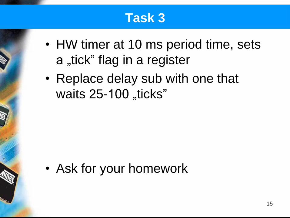
Task 3
• HW timer at 10 ms period time, sets
a „tick” flag in a register
• Replace delay sub with one that
waits 25-100 „ticks”
• Ask for your homework
15