axi bridge for pci express gen3 subsystem v1.0 …...axi bridge for pci express gen3 v1.0 9 pg194...
TRANSCRIPT
AXI Bridge for PCI Express Gen3 Subsystem v1.0Product Guide
Vivado Design Suite
PG194 November 19, 2014
AXI Bridge for PCI Express Gen3 v1.0 www.xilinx.com 2PG194 November 19, 2014
Table of ContentsIP Facts
Chapter 1: OverviewFeature Summary. . . . . . . . . . . . . . . . . . . . . . . . . . . . . . . . . . . . . . . . . . . . . . . . . . . . . . . . . . . . . . . . . . 6Unsupported Features. . . . . . . . . . . . . . . . . . . . . . . . . . . . . . . . . . . . . . . . . . . . . . . . . . . . . . . . . . . . . . 6Limitations . . . . . . . . . . . . . . . . . . . . . . . . . . . . . . . . . . . . . . . . . . . . . . . . . . . . . . . . . . . . . . . . . . . . . . . 6Licensing and Ordering Information . . . . . . . . . . . . . . . . . . . . . . . . . . . . . . . . . . . . . . . . . . . . . . . . . . . 6
Chapter 2: Product SpecificationStandards . . . . . . . . . . . . . . . . . . . . . . . . . . . . . . . . . . . . . . . . . . . . . . . . . . . . . . . . . . . . . . . . . . . . . . . . 9Performance. . . . . . . . . . . . . . . . . . . . . . . . . . . . . . . . . . . . . . . . . . . . . . . . . . . . . . . . . . . . . . . . . . . . . . 9Resource Utilization. . . . . . . . . . . . . . . . . . . . . . . . . . . . . . . . . . . . . . . . . . . . . . . . . . . . . . . . . . . . . . . 10Port Descriptions . . . . . . . . . . . . . . . . . . . . . . . . . . . . . . . . . . . . . . . . . . . . . . . . . . . . . . . . . . . . . . . . . 12Bridge Parameters . . . . . . . . . . . . . . . . . . . . . . . . . . . . . . . . . . . . . . . . . . . . . . . . . . . . . . . . . . . . . . . . 16Memory Map . . . . . . . . . . . . . . . . . . . . . . . . . . . . . . . . . . . . . . . . . . . . . . . . . . . . . . . . . . . . . . . . . . . . 23
Chapter 3: Designing with the CoreGeneral Design Guidelines . . . . . . . . . . . . . . . . . . . . . . . . . . . . . . . . . . . . . . . . . . . . . . . . . . . . . . . . . 34Clocking. . . . . . . . . . . . . . . . . . . . . . . . . . . . . . . . . . . . . . . . . . . . . . . . . . . . . . . . . . . . . . . . . . . . . . . . . 34Resets . . . . . . . . . . . . . . . . . . . . . . . . . . . . . . . . . . . . . . . . . . . . . . . . . . . . . . . . . . . . . . . . . . . . . . . . . . 35AXI Transactions for PCIe . . . . . . . . . . . . . . . . . . . . . . . . . . . . . . . . . . . . . . . . . . . . . . . . . . . . . . . . . . 36Transaction Ordering for PCIe. . . . . . . . . . . . . . . . . . . . . . . . . . . . . . . . . . . . . . . . . . . . . . . . . . . . . . . 36Address Translation . . . . . . . . . . . . . . . . . . . . . . . . . . . . . . . . . . . . . . . . . . . . . . . . . . . . . . . . . . . . . . . 37Interrupts . . . . . . . . . . . . . . . . . . . . . . . . . . . . . . . . . . . . . . . . . . . . . . . . . . . . . . . . . . . . . . . . . . . . . . . 44Malformed TLP. . . . . . . . . . . . . . . . . . . . . . . . . . . . . . . . . . . . . . . . . . . . . . . . . . . . . . . . . . . . . . . . . . . 44Abnormal Conditions. . . . . . . . . . . . . . . . . . . . . . . . . . . . . . . . . . . . . . . . . . . . . . . . . . . . . . . . . . . . . . 44
Chapter 4: Design Flow StepsCustomizing and Generating the Core . . . . . . . . . . . . . . . . . . . . . . . . . . . . . . . . . . . . . . . . . . . . . . . . 49Constraining the Core . . . . . . . . . . . . . . . . . . . . . . . . . . . . . . . . . . . . . . . . . . . . . . . . . . . . . . . . . . . . . 61Simulation . . . . . . . . . . . . . . . . . . . . . . . . . . . . . . . . . . . . . . . . . . . . . . . . . . . . . . . . . . . . . . . . . . . . . . 64Synthesis and Implementation . . . . . . . . . . . . . . . . . . . . . . . . . . . . . . . . . . . . . . . . . . . . . . . . . . . . . . 64
Send Feedback

AXI Bridge for PCI Express Gen3 v1.0 www.xilinx.com 3PG194 November 19, 2014
Chapter 5: Example DesignOverview . . . . . . . . . . . . . . . . . . . . . . . . . . . . . . . . . . . . . . . . . . . . . . . . . . . . . . . . . . . . . . . . . . . . . . . 65Simulation Design Overview . . . . . . . . . . . . . . . . . . . . . . . . . . . . . . . . . . . . . . . . . . . . . . . . . . . . . . . . 65Implementation Design Overview . . . . . . . . . . . . . . . . . . . . . . . . . . . . . . . . . . . . . . . . . . . . . . . . . . . 67Example Design Elements . . . . . . . . . . . . . . . . . . . . . . . . . . . . . . . . . . . . . . . . . . . . . . . . . . . . . . . . . . 68Example Design Output Structure . . . . . . . . . . . . . . . . . . . . . . . . . . . . . . . . . . . . . . . . . . . . . . . . . . . 68
Chapter 6: Test Bench
Appendix A: DebuggingFinding Help on Xilinx.com . . . . . . . . . . . . . . . . . . . . . . . . . . . . . . . . . . . . . . . . . . . . . . . . . . . . . . . . . 71Debug Tools . . . . . . . . . . . . . . . . . . . . . . . . . . . . . . . . . . . . . . . . . . . . . . . . . . . . . . . . . . . . . . . . . . . . . 73Additional Debug Information . . . . . . . . . . . . . . . . . . . . . . . . . . . . . . . . . . . . . . . . . . . . . . . . . . . . . . 75Interface Debug . . . . . . . . . . . . . . . . . . . . . . . . . . . . . . . . . . . . . . . . . . . . . . . . . . . . . . . . . . . . . . . . . . 76
Appendix B: Migrating and UpgradingMigrating to the Vivado Design Suite. . . . . . . . . . . . . . . . . . . . . . . . . . . . . . . . . . . . . . . . . . . . . . . . . 77Migrating from AXI PCIe Gen2 to AXI PCIe Gen3. . . . . . . . . . . . . . . . . . . . . . . . . . . . . . . . . . . . . . . . 77
Appendix C: Additional Resources and Legal NoticesXilinx Resources . . . . . . . . . . . . . . . . . . . . . . . . . . . . . . . . . . . . . . . . . . . . . . . . . . . . . . . . . . . . . . . . . . 79References . . . . . . . . . . . . . . . . . . . . . . . . . . . . . . . . . . . . . . . . . . . . . . . . . . . . . . . . . . . . . . . . . . . . . . 79Revision History . . . . . . . . . . . . . . . . . . . . . . . . . . . . . . . . . . . . . . . . . . . . . . . . . . . . . . . . . . . . . . . . . . 80Please Read: Important Legal Notices . . . . . . . . . . . . . . . . . . . . . . . . . . . . . . . . . . . . . . . . . . . . . . . . 80
Send Feedback

AXI Bridge for PCI Express Gen3 v1.0 www.xilinx.com 4PG194 November 19, 2014 Product Specification
IntroductionThe Xilinx® AXI Endpoint (EP) Bridge for PCI Express® core is an interface between AXI4 and PCI Express.
Features• UltraScale™ architecture and Virtex®-7 XT
FPGA Gen3 Integrated Blocks for PCI Express• Maximum Payload Size (MPS) up to 256 bytes• Multiple Vector Messaged Signaled Interrupts
(MSIs)• Legacy interrupt support• Memory-mapped AXI4 access to PCIe® space• PCIe access to memory-mapped AXI4 space• Tracks and manages Transaction Layer Packets
(TLPs) completion processing• Detects and indicates error conditions with
interrupts• Optimal AXI4 pipeline support for enhanced
performance• Compliant with Advanced RISC Machine
(ARM®) Advanced Microcontroller Bus Architecture 4 (AMBA®) AXI4 specif ication
• Supports up to six PCIe 32-bit or three 64-bit PCIe Base Address Registers (BARs) as Endpoint
IP Facts
Facts Table
Core SpecificsSupported Device Family(1)
UltraScale Architecture, Virtex-7 XT(3)
Supported User Interfaces AXI4
Resources See Resource Utilization
Provided with CoreDesign Files Verilog
Example Design Verilog
Test Bench Verilog
Constraints File XDC
Simulation Model Not Provided
Supported S/W Driver Standalone and Linux
Tested Design Flows(2)
Design EntryVivado® Design Suite
Vivado
Simulation For supported simulators, see theXilinx Design Tools: Release Notes Guide
Synthesis Vivado Synthesis
SupportProvided by Xilinx @ www.xilinx.com/support
Notes: 1. For a complete list of supported devices, see the Vivado IP
catalog. See also Maximum Frequencies.2. For the supported versions of the tools, see the
Xilinx Design Tools: Release Notes Guide.3. Except for XC7VX485T, XC7V585T, and XC7V2000T, Virtex-7
devices are supported.
Send Feedback
AXI Bridge for PCI Express Gen3 v1.0 www.xilinx.com 5PG194 November 19, 2014
Chapter 1
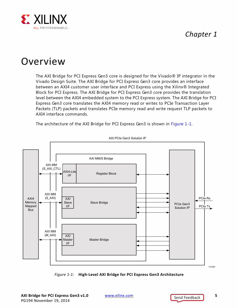
OverviewThe AXI Bridge for PCI Express Gen3 core is designed for the Vivado® IP integrator in the Vivado Design Suite. The AXI Bridge for PCI Express Gen3 core provides an interface between an AXI4 customer user interface and PCI Express using the Xilinx® Integrated Block for PCI Express. The AXI Bridge for PCI Express Gen3 core provides the translation level between the AXI4 embedded system to the PCI Express system. The AXI Bridge for PCI Express Gen3 core translates the AXI4 memory read or writes to PCIe Transaction Layer Packets (TLP) packets and translates PCIe memory read and write request TLP packets to AXI4 interface commands.
The architecture of the AXI Bridge for PCI Express Gen3 is shown in Figure 1-1.
X-Ref Target - Figure 1-1
Figure 1-1: High-Level AXI Bridge for PCI Express Gen3 Architecture
Send Feedback

AXI Bridge for PCI Express Gen3 v1.0 www.xilinx.com 6PG194 November 19, 2014
Chapter 1: Overview
Feature SummaryThe AXI Bridge for PCI Express Gen3 core is an interface between the AXI4 and PCI Express. It contains the memory mapped AXI4 to AXI4-Stream Bridge and the AXI4-Stream Enhanced Interface Block for PCIe. The memory-mapped AXI4 to AXI4-Stream Bridge contains a register block and two functional half bridges, referred to as the Slave Bridge and Master Bridge. The slave bridge connects to the AXI4 Interconnect as a slave device to handle any issued AXI4 master read or write requests. The master bridge connects to the AXI4 Interconnect as a master to process the PCIe generated read or write TLPs. The core uses a set of interrupts to detect and flag error conditions.
The AXI Bridge for PCI Express Gen3 core supports Endpoint configurations.
• When configured as an Endpoint, the AXI Bridge for PCI Express Gen3 core supports up to six 32-bit or three 64-bit PCIe Base Address Registers (BARs).
The AXI Bridge for PCI Express Gen3 core is compliant with the PCI Express Base Specification v2.0 [Ref 7] and with the AMBA® AXI4 specification [Ref 6].
Unsupported FeaturesThe following features are not supported in the AXI Bridge for PCI Express Gen3 core.
• Root Port configurations
• Tandem PROM and Tandem PCIe
Limitations
Reference Clock for PCIe Frequency ValueThe refclk input used by the serial transceiver for PCIe must be 100 MHz, 125 MHz, and 250 MHz. The C_REF_CLK_FREQ parameter is used to set this value, as defined in Table 2-6.
Licensing and Ordering InformationThis Xilinx module is provided at no additional cost with the Xilinx Vivado Design Suite under the terms of the Xilinx End User License.
Send Feedback
AXI Bridge for PCI Express Gen3 v1.0 www.xilinx.com 7PG194 November 19, 2014
Chapter 1: Overview
Information about this and other Xilinx modules is available at the Xilinx Intellectual Property page. For information on pricing and availability of other Xilinx modules and tools, contact your local Xilinx sales representative.
For more information, visit the AXI Bridge for PCI Express Gen3 product page.
Send Feedback

AXI Bridge for PCI Express Gen3 v1.0 www.xilinx.com 8PG194 November 19, 2014
Chapter 2
Product SpecificationThe Register block contains registers used in the AXI Bridge for PCI Express Gen3 core for dynamically mapping the AXI4 memory mapped (MM) address range provided using the AXIBAR parameters to an address for PCIe® range.
The slave bridge provides termination of memory-mapped AXI4 transactions from an AXI master device (such as a processor). The slave bridge provides a way to translate addresses that are mapped within the AXI4 memory mapped address domain to the domain addresses for PCIe. Write transactions to the Slave Bridge are converted into one or more MemWr TLPs, depending on the configured Max Payload Size setting, which are passed to the integrated block for PCI Express. The Slave Bridge can support up to eight active AXI4 memory mapped write transactions.
When a remote AXI master initiates a read transaction to the slave bridge, the read address and qualif iers are captured and a MemRd request TLP is passed to the core and a completion timeout timer is started. Completions received through the core are correlated with pending read requests and read data is returned to the AXI master. The slave bridge is capable of handling up to 32 memory mapped AXI4 read requests with pending completions.
The master bridge processes both PCIe MemWr and MemRd request TLPs received from the integrated block for PCI Express and provides a means to translate addresses that are mapped within the address for PCIe domain to the memory mapped AXI4 address domain. Each PCIe MemWr request TLP header is used to create an address and qualif iers for the memory mapped AXI4 bus and the associated write data is passed to the addressed memory mapped AXI4 Slave. The master bridge can support up to eight active PCIe MemWr request TLPs.
Each PCIe MemRd request TLP header is used to create an address and qualif iers for the memory-mapped AXI4 bus. Read data is collected from the addressed memory mapped AXI4 Slave and used to generate completion TLPs which are then passed to the integrated block for PCI Express. The master bridge can handle up to eight read requests with pending completions for improved AXI4 pipelining performance.
The instantiated AXI4-Stream Enhanced PCIe block contains submodules including the Requester/Completer interfaces to the AXI bridge and the Register block. The Register block contains the status, control, interrupt registers, and the AXI4-Lite interface.
Send Feedback

AXI Bridge for PCI Express Gen3 v1.0 www.xilinx.com 9PG194 November 19, 2014
Chapter 2: Product Specification
StandardsThe AXI Bridge for PCIe core is compliant with the ARM® AMBA® AXI4 Protocol Specification [Ref 6] and the PCI Express Base Specification v2.0 [Ref 7].
PerformanceFigure 2-1 shows a configuration diagram for a target FPGA.
Maximum FrequenciesThe maximum frequency for the AXI clock is 125 MHz for -1 speed grade FPGAs, and 250 MHz for -2 and -3 speed grade FPGAs.
Line Rate Support for PCIe Gen1/Gen2/Gen3The link speed, number of lanes supported, and support of line rate for PCIe are defined in Table 2-1. Achieving line rate for PCIe is dependent on the device family, the AXI clock frequency, the AXI data width, the number of lanes, and Gen1 (2.5 GT/s), Gen2 (5.0 GT/s) or Gen3 (8.0 GT/s) link speed.
X-Ref Target - Figure 2-1
Figure 2-1: FPGA System Configuration Diagram
Send Feedback

AXI Bridge for PCI Express Gen3 v1.0 www.xilinx.com 10PG194 November 19, 2014
Chapter 2: Product Specification
Resource UtilizationThe resource utitlization numbers were generated in the Vivado® Design Suite. Resource utilization numbers for other devices can be generated by implementing the provided example design and checking for the resources used by only the core in the resource utilization report. Variation in tools and optimization settings can result in variance of these reported numbers.
Table 2-1: Line Rate for PCIe Support for Gen1/Gen2/Gen3
Device Family
PCIe Link Speed PCIe Link Width AXI CLK Frequency AXI Data Width
Virtex-7 XT
Gen 1
x162.5 64
125 64
x262.5 64
125 64
x4 125 64
x8125 128
250(1) 64
Gen2
x162.5 64
125 64
x2 125 64
x4125 128
250(1) 64
x8125 256
250(1) 128
Gen3(1)
x1125 64
250 64
x2125 128
250 64
x4125 256
250 128
x8 250 256
Notes: 1. 250 MHz AXI Clock Frequency is not supported for -1 speed grade.2. For 7 Series (Virtex®-7 XT) device speed grade support, see the Virtex-7 FPGAs Gen3 Integrated
Block for PCI Express Product Guide (PG023) [Ref 3].3. For Ultrascale™ architecture device speed grade support, see the UltraScale Architecture Integrated
Block for PCI Express Product Guide (PG156) [Ref 4].
Send Feedback

AXI Bridge for PCI Express Gen3 v1.0 www.xilinx.com 11PG194 November 19, 2014
Chapter 2: Product Specification
Note: The utilization data is generated using the PCI Express example design, which only connects the master AXI interface.
Virtex-7 DevicesTable 2-2 shows the resource utilization for the AXI Bridge for PCI Express Gen3 core for different configurations on the Virtex-7 XC7V690T device.
Virtex UltraScale DevicesTable 2-3 shows the resource utilization for the AXI Bridge for PCIe core for different configurations on the XCVU095-FFVD1924-2-E-ES1 device.
Table 2-2: Resource Utilization Summary
Configuration Slice Registers Slice LUTs
Endpoint x1 Gen1 3182 3982
Endpoint x2 Gen1 3551 4403
Endpoint x4 Gen1 4289 5502
Endpoint x8 Gen1 6374 7686
Endpoint x1 Gen2 3182 3985
Endpoint x2 Gen2 3551 4425
Endpoint x4 Gen2 4795 5646
Endpoint x8 Gen2 7303 8115
Endpoint x1 Gen3 3178 3832
Endpoint x8 Gen3 4053 4628
Endpoint x8 Gen3 5719 6200
Endpoint x8 Gen3 7299 8423
Table 2-3: Resource Utilization Summary
Configuration Slice Registers Slice LUTs
Endpoint x1 Gen1 2892 3472
Endpoint x2 Gen1 3338 3790
Endpoint x4 Gen1 4228 4387
Endpoint x8 Gen1 6472 5776
Endpoint x1 Gen2 3026 3465
Endpoint x2 Gen2 3591 3788
Endpoint x4 Gen2 5049 4615
Endpoint x8 Gen2 7994 6269
Endpoint x1 Gen3 3030 3469
Endpoint x2 Gen3 3921 4014
Send Feedback

AXI Bridge for PCI Express Gen3 v1.0 www.xilinx.com 12PG194 November 19, 2014
Chapter 2: Product Specification
Kintex UltraScale DevicesTable 2-4 shows the resource utilization for the AXI Bridge for PCIe core for different configurations on the XCKU040-FFVA1156-2-E device.
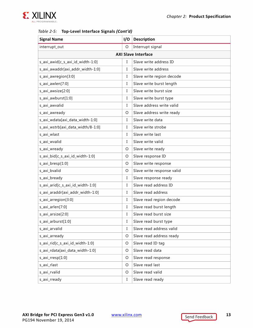
Port DescriptionsThe interface signals for the AXI Bridge for PCI Express Gen3 are described in Table 2-5.
Endpoint x4 Gen3 5601 5027
Endpoint x8 Gen3 7973 6398
Table 2-4: Resource Utilization Summary
Configuration Slice Registers Slice LUTs
Endpoint x1 Gen1 2892 3466
Endpoint x2 Gen1 3338 3790
Endpoint x4 Gen1 4228 4389
Endpoint x8 Gen1 6472 5772
Endpoint x1 Gen2 3026 3467
Endpoint x2 Gen2 3591 3798
Endpoint x4 Gen2 5049 4609
Endpoint x8 Gen2 7994 6278
Endpoint x1 Gen3 3030 3467
Endpoint x2 Gen3 3921 4020
Endpoint x4 Gen3 5601 5034
Endpoint x8 Gen3 7973 6412
Table 2-5: Top-Level Interface Signals
Signal Name I/O Description
Global Signals
refclk I PCIe Reference Clock
sys_rst_n I Reset from the PCIe edge connector reset signal.
axi_aclk O PCIe derived clock output for axi_aclk
axi_ctl_aclk I aclk for the AXI PCIe Ctl Interface. Should be driven by the axi_aclk output.
sys_clk_gt(1) I System Clock
Table 2-3: Resource Utilization Summary (Cont’d)
Configuration Slice Registers Slice LUTs
Send Feedback
AXI Bridge for PCI Express Gen3 v1.0 www.xilinx.com 13PG194 November 19, 2014
Chapter 2: Product Specification
interrupt_out O Interrupt signal
AXI Slave Interface
s_axi_awid[c_s_axi_id_width-1:0] I Slave write address ID
s_axi_awaddr[axi_addr_width-1:0] I Slave write address
s_axi_awregion[3:0] I Slave write region decode
s_axi_awlen[7:0] I Slave write burst length
s_axi_awsize[2:0] I Slave write burst size
s_axi_awburst[1:0] I Slave write burst type
s_axi_awvalid I Slave address write valid
s_axi_awready O Slave address write ready
s_axi_wdata[axi_data_width-1:0] I Slave write data
s_axi_wstrb[axi_data_width/8-1:0] I Slave write strobe
s_axi_wlast I Slave write last
s_axi_wvalid I Slave write valid
s_axi_wready O Slave write ready
s_axi_bid[c_s_axi_id_width-1:0] O Slave response ID
s_axi_bresp[1:0] O Slave write response
s_axi_bvalid O Slave write response valid
s_axi_bready I Slave response ready
s_axi_arid[c_s_axi_id_width-1:0] I Slave read address ID
s_axi_araddr[axi_addr_width-1:0] I Slave read address
s_axi_arregion[3:0] I Slave read region decode
s_axi_arlen[7:0] I Slave read burst length
s_axi_arsize[2:0] I Slave read burst size
s_axi_arburst[1:0] I Slave read burst type
s_axi_arvalid I Slave read address valid
s_axi_arready O Slave read address ready
s_axi_rid[c_s_axi_id_width-1:0] O Slave read ID tag
s_axi_rdata[axi_data_width-1:0] O Slave read data
s_axi_rresp[1:0] O Slave read response
s_axi_rlast O Slave read last
s_axi_rvalid O Slave read valid
s_axi_rready I Slave read ready
Table 2-5: Top-Level Interface Signals (Cont’d)
Signal Name I/O Description
Send Feedback

AXI Bridge for PCI Express Gen3 v1.0 www.xilinx.com 14PG194 November 19, 2014
Chapter 2: Product Specification
AXI Master Interface
m_axi_awaddr[axi_addr_width-1:0] O Master write address
m_axi_awlen[7:0] O Master write burst length
m_axi_awsize[2:0] O Master write burst size
m_axi_awburst[1:0] O Master write burst type
m_axi_awprot[2:0] O Master write protection type
m_axi_awvalid O Master write address valid
m_axi_awready I Master write address ready
m_axi_wdata[axi_data_width-1:0] O Master write data
m_axi_wstrb[axi_data_width/8-1:0] O Master write strobe
m_axi_wlast O Master write last
m_axi_wvalid O Master write valid
m_axi_wready I Master write ready
m_axi_bresp[1:0] I Master write response
m_axi_bvalid I Master write response valid
m_axi_bready O Master response ready
m_axi_araddr[axi_addr_width-1:0] O Master read address
m_axi_arlen[7:0] O Master read burst length
m_axi_arsize[2:0] O Master read burst size
m_axi_arburst[1:0] O Master read burst type
m_axi_arprot[2:0] O Master read protection type
m_axi_arvalid O Master read address valid
m_axi_arready I Master read address ready
m_axi_rdata[axi_data_width-1:0] I Master read data
m_axi_rresp[1:0] I Master read response
m_axi_rlast I Master read last
m_axi_rvalid I Master read valid
m_axi_rready O Master read ready
AXI4-Lite Control Interface
s_axi_ctl_awaddr[31:0] I Slave write address
s_axi_ctl_awvalid I Slave write address valid
s_axi_ctl_awready O Slave write address ready
s_axi_ctl_wdata[31:0] I Slave write data
s_ax_ctl_wstrb[3:0] I Slave write strobe
Table 2-5: Top-Level Interface Signals (Cont’d)
Signal Name I/O Description
Send Feedback

AXI Bridge for PCI Express Gen3 v1.0 www.xilinx.com 15PG194 November 19, 2014
Chapter 2: Product Specification
s_axi_ctl_wvalid I Slave write valid
s_axi_ctl_wready O Slave write ready
s_axi_ctl_bresp[1:0] O Slave write response
s_axi_ctl_bvalid O Slave write response valid
s_axi_ctl_bready I Slave response ready
s_axi_ctl_araddr[31:0] I Slave read address
s_axi_ctl_arvalid I Slave read address valid
s_axi_ctl_arready O Slave read address ready
s_axi_ctl_rdata[31:0] O Slave read data
s_axi_ctl_rresp[1:0] O Slave read response
s_axi_ctl_rvalid O Slave read valid
s_axi_ctl_rready I Slave read ready
MSI Signals
intx_msi_request I
Legacy interrupt input (see c_interrupt_pin) when msi_enable = 0.Initiates a MSI write request when msi_enable = 1.Intx_msi_request is asserted for one clock period.
intx_msi_grant O
Indicates legacy interrupt/MSI grant signal. The intx_msi_grant signal is asserted for one clock period when the interrupt is accepted by the PCIe core.
msi_enable O Indicates when MSI is enabled.
msi_vector_num [4:0] I Indicates MSI vector to send when writing a MSI write request.
msi_vector_width [2:0] O Indicates the size of the MSI f ield (the number of MSI vectors allocated to the device).
PCIe Interface
pci_exp_rxp[pl_link_cap_max_link_width-1:0] I PCIe RX serial interface
pci_exp_rxn[pl_link_cap_max_link_width-1:0] I PCIe RX serial interface
pci_exp_txp[pl_link_cap_max_link_width-1:0] O PCIe TX serial interface
pci_exp_txn[pl_link_cap_max_link_width-1:0] O PCIe TX serial interface
Notes: 1. sys_clk_gt is available for UltraScale architecture devices only.
Table 2-5: Top-Level Interface Signals (Cont’d)
Signal Name I/O Description
Send Feedback

AXI Bridge for PCI Express Gen3 v1.0 www.xilinx.com 16PG194 November 19, 2014
Chapter 2: Product Specification
Bridge ParametersBecause many features in the AXI Bridge for PCI Express Gen3 core design can be parameterized, you can uniquely tailor the implementation of the core using only the resources required for the desired functionality. This approach also achieves the best possible performance with the lowest resource usage.
The parameters defined for the AXI Bridge for PCI Express Gen3 are shown in Table 2-6.
Table 2-6: Top-Level Parameters
Generic Parameter Name Description Allowable Values Default ValueBridge Parameters
PCIE_BLK_LOCN PCIe integrated block location within FPGA
0: X0Y01: X0Y12: X0Y23:X0Y34:X0Y4(1)
5:X0Y5(1)
0
G3 C_COMP_TIMEOUTSelects the slave bridge completion timeout counter value
0: 50 µs1: 50 ms 0
G4 C_INCLUDE_BAROFFSET_REG
Include the registers for high-order bits to be substituted in translation in slave bridge
0: Exclude1: Include 0
G6 C_AXIBAR_NUMNumber of AXI address apertures that can be accessed
1: BAR_0 enabled2: BAR_0, BAR_1 enabled3: BAR_0, BAR_1, BAR_2 enabled4: BAR_0 through BAR_3 enabled5: BAR_0 through BAR_4 enabled6: BAR_0 through BAR_5 enabled
6
G7 C_AXIBAR_0 AXI BAR_0 aperture low address Valid AXI address(3)(4) 0x00000000_
00000000
G8 C_AXIBAR_HIGHADDR_0
AXI BAR_0 aperture high address Valid AXI address(3)(4) 0x00000000_
00000000
G10 C_AXIBAR2PCIEBAR_0Initial address translation from an AXI BAR_0 address to a PCI Express address
Valid address for PCIe(2) 0x00000000_00000000
G11 C_AXIBAR_1 AXI BAR_1 aperture low address Valid AXI address(3)(4) 0x00000000_
00000000
G12 C_AXIBAR_HIGHADDR_1
AXI BAR_1 aperture high address Valid AXI address(3)(4) 0x00000000_
00000000
Send Feedback

AXI Bridge for PCI Express Gen3 v1.0 www.xilinx.com 17PG194 November 19, 2014
Chapter 2: Product Specification
G14 C_AXIBAR2PCIEBAR_1Initial address translation from an AXI BAR_1 address to a PCI Express address
Valid address for PCIe(2) 0x00000000_00000000
G15 C_AXIBAR_2 AXI BAR_2 aperture low address Valid AXI address(3)(4) 0x00000000_
00000000
G16 C_AXIBAR_HIGHADDR_2
AXI BAR_2 aperture high address Valid AXI address(3)(4) 0x00000000_
00000000
G18 C_AXIBAR2PCIEBAR_2
Initial address translation from an AXI BAR_2 address to a PCI Express address Valid address for PCIe(2) 0x00000000_
00000000
G19 C_AXIBAR_3 AXI BAR_3 aperture low address Valid AXI address(3)(4) 0x00000000_
00000000
G20 C_AXIBAR_HIGHADDR_3
AXI BAR_3 aperture high address Valid AXI address(3)(4) 0x00000000_
00000000
G22 C_AXIBAR2PCIEBAR_3Initial address translation from an AXI BAR_3 address to a PCI Express address
Valid address for PCIe(2) 0x00000000_00000000
G23 C_AXIBAR_4 AXI BAR_4 aperture low address Valid AXI address(3)(4) 0x00000000_
00000000
G24 C_AXIBAR_HIGHADDR_4
AXI BAR_4 aperture high address Valid AXI address(3)(4) 0x00000000_
00000000
G26 C_AXIBAR2PCIEBAR_4Initial address translation from an AXI BAR_4 address to a PCI Express address
Valid address for PCIe(2) 0x00000000_00000000
G27 C_AXIBAR_5 AXI BAR_5 aperture low address Valid AXI address(3)(4) 0x00000000_
00000000
G28 C_AXIBAR_HIGHADDR_5
AXI BAR_5 aperture high address Valid AXI address(3)(4) 0x00000000_
00000000
G30 C_AXIBAR2PCIEBAR_5Initial address translation from an AXI BAR_5 address to a PCI Express address
Valid address for PCIe(2) 0x00000000_00000000
G31 C_PCIEBAR_NUMNumber of address for PCIe apertures that can be accessed
1: BAR_0 enabled2: BAR_[0:1] enabled or BAR_1 as 64-bit3: BAR_[0-2] enabled4: BAR_[0-3] enabled or BAR_2 as 64-bit5: BAR_[0-4] enabled or6: BAR_[0-5] enabled or BAR_4 as 64-bit
3
Table 2-6: Top-Level Parameters (Cont’d)
Generic Parameter Name Description Allowable Values Default Value
Send Feedback

AXI Bridge for PCI Express Gen3 v1.0 www.xilinx.com 18PG194 November 19, 2014
Chapter 2: Product Specification
G33 PF0_BAR0_APERTURE_SIZE
Specifies the size of the PCIe BAR
0x05: 4 Kilobytes0x06: 8 Kilobytes...0x0C: 512 Kilobytes0x0D: 1 Megabyte...0x16: 512 Megabytes0x17: 1 Gigabyte...0x1F: 156 Gigabytes
0x05
PF0_BAR0_CONTROL PCI express control settings for BAR0
bit 0: • 32-bit addressable = 0• 64-bit addressable = 1bit 1: • Prefetchable off = 0• Prefectable on = 1bit 2: • IO BAR = 0• Memory bar = 1
100
G34 C_PCIEBAR2AXIBAR_0Initial address translation from an AXI BAR_0 address to a PCI Express address
Valid AXI address 0x00000000_00000000
C_PCIEBAR2AXIBAR_0_SEC
Defines the AXIBAR memory space (PCIe BAR_0) (accessible from PCIe) to be either secure or non-secure memory mapped.
0: Denotes a non-secure memory space1: Marks the AXI memory space as secure
0
G35 PF0_BAR1_APERTURE_SIZE
Specifies the size of the PCIe BAR.
0x05: 4 Kilobytes0x06: 8 Kilobytes...0x0C: 512 Kilobytes0x0D: 1 Megabyte...0x16: 512 Megabytes0x17: 1 Gigabyte...0x1F: 156 Gigabytes
0x05
Table 2-6: Top-Level Parameters (Cont’d)
Generic Parameter Name Description Allowable Values Default Value
Send Feedback

AXI Bridge for PCI Express Gen3 v1.0 www.xilinx.com 19PG194 November 19, 2014
Chapter 2: Product Specification
PF0_BAR1_CONTROL PCI express control settings for BAR1
bit 0: • 32-bit addressable = 0• 64-bit addressable = 1bit 1: • Prefetchable off=0• Prefectable on =1bit 2: • IO bar=0• Memory bar=1
100
G36 C_PCIEBAR2AXIBAR_1Initial address translation from an AXI BAR_1 address to a PCI Express address
Valid AXI address 0x00000000_00000000
C_PCIEBAR2AXIBAR_1_SEC
Defines the AXIBAR memory space (PCIe BAR_1) (accessible from PCIe) to be either secure or non-secure memory mapped.
0: Denotes a non-secure memory space1: Marks the AXI memory space as secure
0
G37 PF0_BAR2_APERTURE_SIZE
Specifies the size of the PCIe BAR.
0x05: 4 Kilobytes0x06: 8 Kilobytes...0x0C: 512 Kilobytes0x0D: 1 Megabyte...0x16: 512 Megabytes0x17: 1 Gigabyte...0x1F: 156 Gigabytes
0x05
PF0_BAR2_CONTROL PCI express control settings for BAR2
bit 0: • 32-bit addressable = 0• 64-bit addressable = 1bit 1: • Prefetchable off=0• Prefectable on =1bit 2: • IO bar=0• Memory bar=1
100
G38 C_PCIEBAR2AXIBAR_2Initial address translation from an AXI BAR_2 address to a PCI Express address.
Valid AXI address 0x00000000_00000000
C_PCIEBAR2AXIBAR_2_SEC
Defines the AXIBAR memory space (PCIe BAR_2) (accessible from PCIe) to be either secure or non-secure memory mapped.
0: Denotes a non-secure memory space1: Marks the AXI memory space as secure
0
Table 2-6: Top-Level Parameters (Cont’d)
Generic Parameter Name Description Allowable Values Default Value
Send Feedback

AXI Bridge for PCI Express Gen3 v1.0 www.xilinx.com 20PG194 November 19, 2014
Chapter 2: Product Specification
PF0_BAR3_APERTURE_SIZE
Specifies the size of the PCIe BAR.
0x05: 4 Kilobytes0x06: 8 Kilobytes...0x0C: 512 Kilobytes0x0D: 1 Megabyte...0x16: 512 Megabytes0x17: 1 Gigabyte...0x1F: 156 Gigabytes
0x05
PF0_BAR3_CONTROL PCI express control settings for BAR3
bit 0: • 32-bit addressable = 0• 64-bit addressable = 1bit 1: • Prefetchable off=0• Prefectable on =1bit 2: • IO bar=0• Memory bar=1
100
C_PCIEBAR2AXIBAR_3Initial address translation from an AXI BAR_3 address to a PCI Express address.
Valid AXI address 0x00000000_00000000
C_PCIEBAR2AXIBAR_3_SEC
Defines the AXIBAR memory space (PCIe BAR_3) (accessible from PCIe) to be either secure or non-secure memory mapped.
0: Denotes a non-secure memory space1: Marks the AXI memory space as secure
0
PF0_BAR4_APERTURE_SIZE
Specifies the size of the PCIe BAR.
0x05: 4 Kilobytes0x06: 8 Kilobytes...0x0C: 512 Kilobytes0x0D: 1 Megabyte...0x16: 512 Megabytes0x17: 1 Gigabyte...0x1F: 156 Gigabytes
0x05
Table 2-6: Top-Level Parameters (Cont’d)
Generic Parameter Name Description Allowable Values Default Value
Send Feedback

AXI Bridge for PCI Express Gen3 v1.0 www.xilinx.com 21PG194 November 19, 2014
Chapter 2: Product Specification
PF0_BAR4_CONTROL PCI express control settings for BAR4
bit 0: • 32-bit addressable = 0• 64-bit addressable = 1bit 1: • Prefetchable off=0• Prefectable on =1bit 2: • IO bar=0• Memory bar=1
100
C_PCIEBAR2AXIBAR_4Initial address translation from an AXI BAR_4 address to a PCI Express address.
Valid AXI address 0x00000000_00000000
C_PCIEBAR2AXIBAR_4_SEC
Defines the AXIBAR memory space (PCIe BAR_4) (accessible from PCIe) to be either secure or non-secure memory mapped.
0: Denotes a non-secure memory space1: Marks the AXI memory space as secure
0
PF0_BAR5_APERTURE_SIZE
Specifies the size of the PCIe BAR.
0x05: 4 Kilobytes0x06: 8 Kilobytes...0x0C: 512 Kilobytes0x0D: 1 Megabyte...0x16: 512 Megabytes0x17: 1 Gigabyte...0x1F: 156 Gigabytes
0x05
PF0_BAR5_CONTROL PCI express control settings for BAR5
bit 0: • 32-bit addressable = 0• 64-bit addressable = 1bit 1: • Prefetchable off=0• Prefectable on =1bit 2: • IO bar=0• Memory bar=1
100
C_PCIEBAR2AXIBAR_5Initial address translation from an AXI BAR_5 address to a PCI Express address.
Valid AXI address 0x00000000_00000000
C_PCIEBAR2AXIBAR_5_SEC
Defines the AXIBAR memory space (PCIe BAR_5) (accessible from PCIe) to be either secure or non-secure memory mapped.
0: Denotes a non-secure memory space1: Marks the AXI memory space as secure
0
Table 2-6: Top-Level Parameters (Cont’d)
Generic Parameter Name Description Allowable Values Default Value
Send Feedback

AXI Bridge for PCI Express Gen3 v1.0 www.xilinx.com 22PG194 November 19, 2014
Chapter 2: Product Specification
AXI4-Lite Parameters
G39 C_BASEADDR
Device base address
Note: When configured as an RP, the minimum alignment granularity must be 256 MB. Bit [27:0] are used for Bus Number, Device Number, Function number.
Valid AXI address 0xFFFF_FFFF
G40 C_HIGHADDR Device high address Valid AXI address 0x0000_0000
C_S_AXI_CTL_PROTOCOL
AXI4-Lite port connection definition to AXI Interconnect in the Vivado IP integrator.
AXI4LITE AXI4LITE
Core for PCIe Configuration Parameters
G41 PL_LINK_CAP_MAX_LINK_WIDTH Number of PCIe Lanes 1, 2, 4, 8 1
G42 PF0_DEVICE_ID Device ID 16-bit vector 0x0000
G43 PF0_VENDOR_ID Vendor ID 16-bit vector 0x0000
G44 PF0_CLASS_CODE Class Code 24-bit vector 0x00_0000
G45 PF0_REVISION_ID Rev ID 8-bit vector 0x00
G46 C_SUBSYSTEM_ID Subsystem ID 16-bit vector 0x0000
G47 C_SUBSYSTEM_VENDOR_ID Subsystem Vendor ID 16-bit vector 0x0000
G49 REF_CLK_FREQREFCLK inputFrequency
0: 100 MHz1: 125 MHz2: 250 MHz
0
C_NUM_MSI_REQ
Specifies the size of the MSI request vector for selecting the number of requested message values.
0-5 0
Memory Mapped AXI4 Parameters
G50 AXI_DATA_WIDTH AXI Bus Data width.64128256
64
G51 AXI_ADDR_WIDTH AXI Bus Address width. 32-64 32
G52 C_S_AXI_ID_WIDTH AXI Slave Bus ID width 4 4
G55 C_MAX_LINK_SPEED
Maximum PCIe link speed supported
0: 2.5 GT/s1: 5.0 GT/s
0
Table 2-6: Top-Level Parameters (Cont’d)
Generic Parameter Name Description Allowable Values Default Value
Send Feedback

AXI Bridge for PCI Express Gen3 v1.0 www.xilinx.com 23PG194 November 19, 2014
Chapter 2: Product Specification
Memory MapThe memory map shown in Table 2-7 shows the address mapping for the AXI Bridge for PCI Express Gen3 core. These registers are described in more detail in the following section. All registers are accessed through the AXI4-Lite Control Interface and are offset from C_BASEADDR. During a reset, all registers return to default values.
G56 C_INTERRUPT_PIN Legacy INTX pin support/select
0: No INTX support (setting for Root Port)1: INTA selected (only allowable when core in Endpoint configuration)
0
AXI4 Slave Interconnect Parameters(5)
G57 NUM_WRITE_OUTSTANDING
AXI Interconnect Slave Port Write Pipeline Depth
1: Only one active AXI AWADDR can be accepted in the AXI slave bridge for PCIe2: Maximum of two active AXI AWADDR values can be stored in AXI slave bridge for PCIe
2
G58 NUM_READ_OUTSTANDING
AXI Interconnect Slave Port Read Pipeline Depth
1: Only one active AXI ARADDR can be accepted in AXI slave bridge PCIe.2, 4, 8: Size of pipeline for active AXI ARADDR values to be stored in AXI slave bridge PCIe
8
AXI4 Master Interconnect Parameters(5)
G59 NUM_WRITE_OUTSTANDING
AXI Interconnect master bridge write address issue depth
1, 2, 4: Number of actively issued AXI AWADDR values on the AXI Interconnect to the target slave device(s).
4
G60 NUM_READ_OUTSTANDING
AXI Interconnect master bridge read address issue depth
1, 2, 4: Number of actively issued AXI ARADDR values on the AXI Interconnect to the target slave device(s).
4
Notes: 1. X0Y4 and X0Y5 are required for UltraScale devices.2. The width of this should match the address width of the PCIe BARs.3. The range specif ied must comprise a complete, contiguous power of two range, such that the range = 2n and the n least
signif icant bits of the Base Address are zero.4. The difference between C_AXIBAR_n and C_AXIBAR_HIGHADDR_n must be greater than or equal to 0x00000000_00000FFF.5. These are the user parameters of the AXI4 Interconnect. By default, the slave bridge handles up to two AXI4 write requests and
eight AXI4 read requests. The master bridge handles up to four PCIe write/read requests.
Table 2-6: Top-Level Parameters (Cont’d)
Generic Parameter Name Description Allowable Values Default Value
Send Feedback

AXI Bridge for PCI Express Gen3 v1.0 www.xilinx.com 24PG194 November 19, 2014
Chapter 2: Product Specification
PCIe Configuration Space HeaderThe PCIe Configuration Space Header is a memory aperture for accessing the core for PCIe configuration space. This area is read-only when configured as an Endpoint. Special access modes can be enabled using the PHY Status/Control register. All reserved or undefined memory-mapped addresses must return zero and writes have no effect.
Bridge Info Register (Offset 0x130)The Bridge Info register (described in Table 2-8) provides general configuration information about the AXI4-Stream Bridge. Information in this register is static and does not change during operation.
Table 2-7: Register Memory Map
Accessibility Offset Contents Location
RO - EP 0x000 - 0x12F PCIe Configuration Space Header Part of integrated PCIe configuration space.
RO 0x130 Bridge Info
AXI bridge defined memory-mapped register space.
RO - EP 0x134 Bridge Status and Control
R/W 0x138 Interrupt Decode
R/W 0x13C Interrupt Mask
RO - EP 0x140 Bus Location
RO 0x144 Physical-Side Interface (PHY) Status/Control
RO - EP 0x148 Reserved
RO - EP 0x14C Reserved
RO - EP 0x150 Reserved
RO - EP 0x154 Reserved
RO - EP 0x158 Reserved
RO - EP 0x15C Reserved
R/W 0x160 Interrupt Decode 2
R/W 0x164 Interrupt Mask 2
RO 0x168 - 0x1FF Reserved (zeros returned on read)
RO 0x200 VSEC Capability 2
RO 0x204 VSEC Header 2
R/W 0x208 - 0x234 AXI Base Address Translation Configuration Registers
AXI bridge defined memory-mapped space.
RO 0x238 - 0xFFF Reserved (zeros returned on read)
Send Feedback

AXI Bridge for PCI Express Gen3 v1.0 www.xilinx.com 25PG194 November 19, 2014
Chapter 2: Product Specification
Bridge Status and Control Register (Offset 0x134) The Bridge Status and Control register (described in Table 2-9) provides information about the current state of the AXI4-Stream Bridge. It also provides control over how reads and writes to the Core Configuration Access aperture are handled.
Interrupt Decode Register (Offset 0x138)The Interrupt Decode register (described in Table 2-10) provides a single location where the host processor interrupt service routine can determine what is causing the interrupt to be asserted and how to clear the interrupt. Writing a 1'b1 to any bit of the Interrupt Decode register clears that bit except for the Correctable, Non-Fatal, and Fatal bits.
Follow this sequence to clear the Correctable, Non-Fatal, and Fatal bits:
1. Clear the Root Port Error FIFO (0x154) by performing f irst a read, followed by write-back of the same register.
Table 2-8: Bridge Info Register
Bits Name Core Access
Reset Value Description
0 Gen2 Capable RO 0 If set, indicates the link is Gen2 capable. Underlying integrated block and Link partner support PCIe Gen2 speed.
1 Reserved RO 0 Reserved
2 Reserved RO Reserved
15:3 Reserved RO 0 Reserved
18:16 Reserved RO 0 Reserved
31:19 Reserved RO 0 Reserved
Table 2-9: Bridge Status and Control Register
Bits Name Core Access
Reset Value Description
0 ECAM Busy RO 0 Indicates an ECAM access is in progress (waiting for completion).
7:1 Reserved RO 0 Reserved
8Global Disable
RW 0 When set, disables interrupt line from being asserted. Does not prevent bits in Interrupt Decode register from being set.
15:9 Reserved RO 0 Reserved
16 RW1C as RW RW 0 When set, allows writing to core registers which are normally RW1C.
17 Reserved RW 0 Reserved
31:18 Reserved RO 0 Reserved
Send Feedback

AXI Bridge for PCI Express Gen3 v1.0 www.xilinx.com 26PG194 November 19, 2014
Chapter 2: Product Specification
2. Write to the Interrupt Decode Register (0x138) with 1 to the appropriate error bit to clear it.
IMPORTANT: An asserted bit in the Interrupt Decode register does not cause the interrupt line to assert unless the corresponding bit in the Interrupt Mask register is also set.
Table 2-10: Interrupt Decode Register
Bits Name Core Access
Reset Value Description
0 Link Down RW1C 0 Indicates that Link-Up on the PCI Express link was lost. Not asserted unless link-up had previously been seen.
1 Reserved RW1C 0 Reserved
2 Streaming Error RW1C 0 Indicates a gap was encountered in a streamed packet on the TX interface (RW, RR, or CC).
3 Hot Reset RW1C 0 Indicates a Hot Reset was detected.
4 Reserved RO 0 Reserved
7:5 Cfg Completion Status RW1C 0 Indicates config completion status.
8 Cfg Timeout RW1C 0 Indicates timeout on an ECAM access. (Only applicable to Root Port cores.)
9 Correctable RW1C 0
Indicates a correctable error message was received.Requester ID of error message should be read from the Root Port FIFO.(Only applicable to Root Port cores.)
10 Non-Fatal RW1C 0
Indicates a non-fatal error message was received. Requester ID of error message should be read from the Root Port FIFO.(Only applicable to Root Port cores.)
11 Fatal RW1C 0
Indicates a fatal error message was received. Requester ID of error message should be read from the Root Port FIFO.(Only applicable to Root Port cores.)
15:12 Reserved RO 0 Reserved
16 INTx Interrupt Received RW1C 0
Indicates an INTx interrupt was received.Interrupt details should be read from the Root Port FIFO. (Only applicable to Root Port cores.)
17 MSI Interrupt Received RW1C 0
Indicates an MSI(x) interrupt was received.Interrupt details should be read from the Root Port FIFO. (Only applicable to Root Port cores.)
19:18 Reserved RO 0 Reserved
20Slave Unsupported Request
RW1C 0 Indicates that a completion TLP was received with a status of 0b001 - Unsupported Request.
21 Slave Unexpected Completion RW1C 0 Indicates that a completion TLP was received that was
unexpected.
Send Feedback

AXI Bridge for PCI Express Gen3 v1.0 www.xilinx.com 27PG194 November 19, 2014
Chapter 2: Product Specification
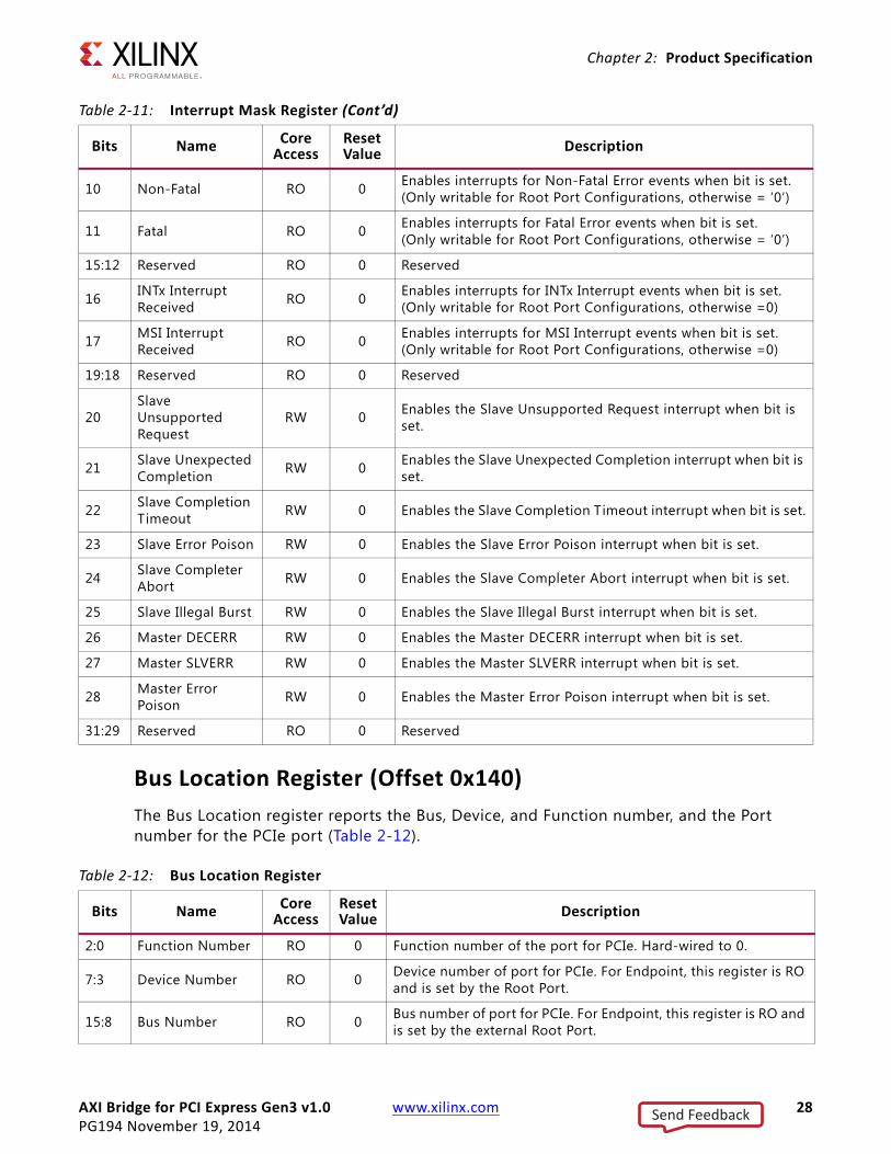
Interrupt Mask Register (Offset 0x13C)The Interrupt Mask register controls whether each individual interrupt source can cause the interrupt line to be asserted. A one in any location allows the interrupt source to assert the interrupt line. The Interrupt Mask register initializes to all zeros. Therefore, by default no interrupt is generated for any event. Table 2-11 describes the Interrupt Mask register bits and values.
22 Slave Completion Timeout RW1C 0
Indicates that the expected completion TLP(s) for a read request for PCIe was not returned within the time period selected by the C_COMP_TIMEOUT parameter.
23 Slave Error Poison RW1C 0 Indicates the EP bit was set in a completion TLP.
24 Slave Completer Abort RW1C 0 Indicates that a completion TLP was received with a status of
0b100 - Completer Abort.
25 Slave Illegal Burst RW1C 0 Indicates that a burst type other than INCR was requested by the AXI master.
26 Master DECERR RW1C 0 Indicates a Decoder Error (DECERR) response was received.
27 Master SLVERR RW1C 0 Indicates a Slave Error (SLVERR) response was received.
28 Master Error Poison RW1C 0 Indicates an EP bit was set in a MemWR TLP for PCIe.
31:29 Reserved RO 0 Reserved
Table 2-10: Interrupt Decode Register (Cont’d)
Bits Name Core Access
Reset Value Description
Table 2-11: Interrupt Mask Register
Bits Name Core Access
Reset Value Description
0 Link Down RW 0 Enables interrupts for Link Down events when bit is set.
1 ECRC Error RW 0 Enables interrupts for ECRC Error events when bit is set.(Only writable for EP configurations, otherwise = ‘0’)
2 Streaming Error RW 0 Enables interrupts for Streaming Error events when bit is set.
3 Hot Reset RW 0 Enables interrupts for Hot Reset events when bit is set.(Only writable for EP configurations, otherwise = ‘0’)
4 Reserved RO 0 Reserved
7:5 Cfg Completion Status RW 0 Enables interrupts for config completion status.
(Only writable for Root Port Configurations, otherwise = ‘0’)
8 Cfg Timeout RO 0Enables interrupts for Config (Cfg) Timeout events when bit is set.(Only writable for Root Port Configurations, otherwise = ‘0’)
9 Correctable RO 0 Enables interrupts for Correctable Error events when bit is set.(Only writable for Root Port Configurations, otherwise = ‘0’)
Send Feedback
AXI Bridge for PCI Express Gen3 v1.0 www.xilinx.com 28PG194 November 19, 2014
Chapter 2: Product Specification
Bus Location Register (Offset 0x140)The Bus Location register reports the Bus, Device, and Function number, and the Port number for the PCIe port (Table 2-12).
10 Non-Fatal RO 0 Enables interrupts for Non-Fatal Error events when bit is set.(Only writable for Root Port Configurations, otherwise = ‘0’)
11 Fatal RO 0 Enables interrupts for Fatal Error events when bit is set.(Only writable for Root Port Configurations, otherwise = ‘0’)
15:12 Reserved RO 0 Reserved
16 INTx Interrupt Received RO 0 Enables interrupts for INTx Interrupt events when bit is set.
(Only writable for Root Port Configurations, otherwise =0)
17 MSI Interrupt Received RO 0 Enables interrupts for MSI Interrupt events when bit is set.
(Only writable for Root Port Configurations, otherwise =0)
19:18 Reserved RO 0 Reserved
20Slave Unsupported Request
RW 0 Enables the Slave Unsupported Request interrupt when bit is set.
21 Slave Unexpected Completion RW 0 Enables the Slave Unexpected Completion interrupt when bit is
set.
22 Slave Completion Timeout RW 0 Enables the Slave Completion Timeout interrupt when bit is set.
23 Slave Error Poison RW 0 Enables the Slave Error Poison interrupt when bit is set.
24 Slave Completer Abort RW 0 Enables the Slave Completer Abort interrupt when bit is set.
25 Slave Illegal Burst RW 0 Enables the Slave Illegal Burst interrupt when bit is set.
26 Master DECERR RW 0 Enables the Master DECERR interrupt when bit is set.
27 Master SLVERR RW 0 Enables the Master SLVERR interrupt when bit is set.
28 Master Error Poison RW 0 Enables the Master Error Poison interrupt when bit is set.
31:29 Reserved RO 0 Reserved
Table 2-11: Interrupt Mask Register (Cont’d)
Bits Name Core Access
Reset Value Description
Table 2-12: Bus Location Register
Bits Name Core Access
Reset Value Description
2:0 Function Number RO 0 Function number of the port for PCIe. Hard-wired to 0.
7:3 Device Number RO 0 Device number of port for PCIe. For Endpoint, this register is RO and is set by the Root Port.
15:8 Bus Number RO 0 Bus number of port for PCIe. For Endpoint, this register is RO and is set by the external Root Port.
Send Feedback

AXI Bridge for PCI Express Gen3 v1.0 www.xilinx.com 29PG194 November 19, 2014
Chapter 2: Product Specification
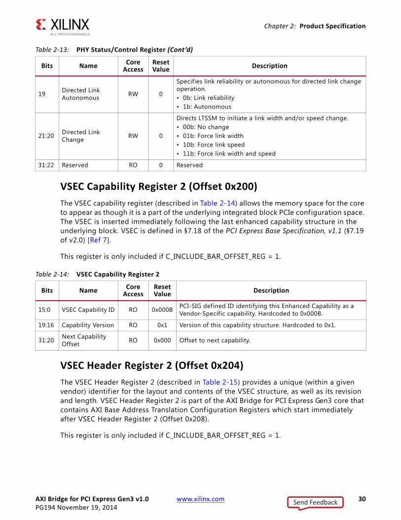
PHY Status/Control Register (Offset 0x144)The PHY Status/Control register (described in Table 2-13) provides the status of the current PHY state, as well as control of speed and rate switching for Gen2-capable cores.
23:16 Port Number RW 0 Sets the Port number field of the Link Capabilities register.
31:24 Reserved RO 0 Reserved
Table 2-12: Bus Location Register
Bits Name Core Access
Reset Value Description
Table 2-13: PHY Status/Control Register
Bits Name Core Access
Reset Value Description
0 Link Rate RO 0 Reports the current link rate. 0b = 2.5 GT/s, 1b = 5.0 GT/s.
2:1 Link Width RO 0 Reports the current link width. 00b = x1, 01b = x2, 10b = x4, 11b = x8.
8:3 LTSSM State RO 0Reports the current Link Training and Status State Machine (LTSSM) state. Encoding is specific to the underlying integrated block.
10:9 Lane Reversal RO 0
Reports the current lane reversal mode.• 00b: No reversal• 01b: Lanes 1:0 reversed• 10b: Lanes 3:0 reversed• 11b: Lanes 7:0 reversed
11 Link Up RO 0
Reports the current PHY Link-up state.• 1b: Link up• 0b: Link downLink up indicates the core has achieved link up status, meaning the LTSSM is in the L0 state and the core can send/receive data packets.
15:12 Reserved RO 0 Reserved
17:16 Directed Link Width RW 0
Specifies completer link width for a directed link change operation. Only acted on when Directed Link Change specifies a width change.• 00b: x1• 01b: x2• 10b: x4• 11b: x8
18 Directed Link Speed RW 0
Specifies completer link speed for a directed link change operation. Only acted on when Directed Link Change specifies a speed change.• 0b: 2.5 GT/s• 1b: 5.0 GT/s
Send Feedback
AXI Bridge for PCI Express Gen3 v1.0 www.xilinx.com 30PG194 November 19, 2014
Chapter 2: Product Specification
VSEC Capability Register 2 (Offset 0x200) The VSEC capability register (described in Table 2-14) allows the memory space for the core to appear as though it is a part of the underlying integrated block PCIe configuration space. The VSEC is inserted immediately following the last enhanced capability structure in the underlying block. VSEC is defined in §7.18 of the PCI Express Base Specification, v1.1 (§7.19 of v2.0) [Ref 7].
This register is only included if C_INCLUDE_BAR_OFFSET_REG = 1.
VSEC Header Register 2 (Offset 0x204)The VSEC Header Register 2 (described in Table 2-15) provides a unique (within a given vendor) identif ier for the layout and contents of the VSEC structure, as well as its revision and length. VSEC Header Register 2 is part of the AXI Bridge for PCI Express Gen3 core that contains AXI Base Address Translation Configuration Registers which start immediately after VSEC Header Register 2 (Offset 0x208).
This register is only included if C_INCLUDE_BAR_OFFSET_REG = 1.
19 Directed Link Autonomous RW 0
Specifies link reliability or autonomous for directed link change operation.• 0b: Link reliability• 1b: Autonomous
21:20 Directed Link Change RW 0
Directs LTSSM to initiate a link width and/or speed change.• 00b: No change• 01b: Force link width• 10b: Force link speed• 11b: Force link width and speed
31:22 Reserved RO 0 Reserved
Table 2-13: PHY Status/Control Register (Cont’d)
Bits Name Core Access
Reset Value Description
Table 2-14: VSEC Capability Register 2
Bits Name Core Access
Reset Value Description
15:0 VSEC Capability ID RO 0x000B PCI-SIG defined ID identifying this Enhanced Capability as a Vendor-Specific capability. Hardcoded to 0x000B.
19:16 Capability Version RO 0x1 Version of this capability structure. Hardcoded to 0x1.
31:20 Next Capability Offset RO 0x000 Offset to next capability.
Send Feedback

AXI Bridge for PCI Express Gen3 v1.0 www.xilinx.com 31PG194 November 19, 2014
Chapter 2: Product Specification
AXI Base Address Translation Configuration Registers (Offset 0x208 - 0x234)The AXI Base Address Translation Configuration Registers and their offsets are shown in Table 2-16 and the register bits are described in Table 2-17. This set of registers can be used in two configurations based on the address width of the PCIe BARs. When the PCIe BAR is set to a 32-bit address space, then the translation vector should be placed into the AXIBAR2PCIEBAR_nL register where n is the PCIe BAR number. When the BAR is set to a 64-bit address space, then the most significant 32 bits are written into the AXIBAR2PCIEBAR_nU and the least significant 32 bits are written into AXIBAR2PCIEBAR_nL. These registers are only included if C_INCLUDE_BAR_OFFSET_REG = 1. Care should be taken so that invalid values are not written to the address translation registers.
Table 2-15: VSEC Header Register 2
Bits Name Core Access Reset Value Description
15:0 VSEC ID RO 0x0002 ID value uniquely identifying the nature and format of this VSEC structure.
19:16 VSEC REV RO 0x0 Version of this capability structure. Hardcoded to 0x0.
31:20 VSEC Length RO 0x038Length of the entire VSEC Capability structure, in bytes, including the VSEC Capability register. Hardcoded to 0x038 (56 decimal).
Table 2-16: AXI Base Address Translation Configuration Registers
Offset Bits Register Mnemonic
0x208 31-0 AXIBAR2PCIEBAR_0U
0x20C 31-0 AXIBAR2PCIEBAR_0L
0x210 31-0 AXIBAR2PCIEBAR_1U
0x214 31-0 AXIBAR2PCIEBAR_1L
0x218 31-0 AXIBAR2PCIEBAR_2U
0x21C 31-0 AXIBAR2PCIEBAR_2L
0x220 31-0 AXIBAR2PCIEBAR_3U
0x224 31-0 AXIBAR2PCIEBAR_3L
0x228 31-0 AXIBAR2PCIEBAR_4U
0x22C 31-0 AXIBAR2PCIEBAR_4L
0x230 31-0 AXIBAR2PCIEBAR_5U
0x234 31-0 AXIBAR2PCIEBAR_5L
Send Feedback

AXI Bridge for PCI Express Gen3 v1.0 www.xilinx.com 32PG194 November 19, 2014
Chapter 2: Product Specification
Table 2-17: AXI Base Address Translation Configuration Register Bit Definitions
Bits Name Core Access Reset Value Description
31-0LowerAddress
R/W C_AXIBAR2PCIEBAR_0(31 to 0)To create the address for PCIe–this is the value substituted for the least significant 32 bits of the AXI address.
31-0 Upper Address R/W
if (C_AXIBAR2PCIEBAR_0 = 64 bits), thenreset value = C_AXIBAR2PCIEBAR_0(63 to 32)
if (C_AXIBAR2PCIEBAR_0 = 32 bits), thenreset value = 0x00000000
To create the address for PCIe–this is the value substituted for the most significant 32 bits of the AXI address.
31-0LowerAddress
R/W C_AXIBAR2PCIEBAR_1(31 to 0)To create the address for PCIe–this is the value substituted for the least significant 32 bits of the AXI address.
31-0 Upper Address R/W
if (C_AXIBAR2PCIEBAR_1 = 64 bits), thenreset value = C_AXIBAR2PCIEBAR_1(63 to 32)
if (C_AXIBAR2PCIEBAR_1 = 32 bits), thenreset value = 0x00000000
To create the address for PCIe– this is the value substituted for the most significant 32 bits of the AXI address.
31-0LowerAddress
R/W C_AXIBAR2PCIEBAR_2(31 to 0)To create the address for PCIe–this is the value substituted for the least significant 32 bits of the AXI address.
31-0 Upper Address R/W
if (C_AXIBAR2PCIEBAR_2 = 64 bits), thenreset value = C_AXIBAR2PCIEBAR_2(63 to 32)
if (C_AXIBAR2PCIEBAR_2 = 32 bits), thenreset value = 0x00000000
To create the address for PCIe–this is the value substituted for the most significant 32 bits of the AXI address.
31-0LowerAddress
R/W C_AXIBAR2PCIEBAR_3(31 to 0)To create the address for PCIe–this is the value substituted for the least significant 32 bits of the AXI address.
31-0 Upper Address R/W
if (C_AXIBAR2PCIEBAR_3 = 64 bits) thenreset value = C_AXIBAR2PCIEBAR_3(63 to 32)
if (C_AXIBAR2PCIEBAR_3 = 32 bits) thenreset value = 0x00000000
To create the address for PCIe–this is the value substituted for the most significant 32 bits of the AXI address.
31-0LowerAddress
R/W C_AXIBAR2PCIEBAR_4(31 to 0)To create the address for PCIe–this is the value substituted for the least significant 32 bits of the AXI address.
Send Feedback

AXI Bridge for PCI Express Gen3 v1.0 www.xilinx.com 33PG194 November 19, 2014
Chapter 2: Product Specification
31-0 Upper Address R/W
if (C_AXIBAR2PCIEBAR_4 = 64 bits), thenreset value = C_AXIBAR2PCIEBAR_4(63 to 32)
if (C_AXIBAR2PCIEBAR_4 = 32 bits), thenreset value = 0x00000000
To create the address for PCIe–this is the value substituted for the most significant 32 bits of the AXI address.
31-0LowerAddress
R/W C_AXIBAR2PCIEBAR_5(31 to 0)To create the address for PCIe–this is the value substituted for the least significant 32 bits of the AXI address.
31-0 Upper Address R/W
if (C_AXIBAR2PCIEBAR_5 = 64 bits), thenreset value = C_AXIBAR2PCIEBAR_5(63 to 32)
if (C_AXIBAR2PCIEBAR_5 = 32 bits), thenreset value = 0x00000000
To create the address for PCIe–this is the value substituted for the most significant 32 bits of the AXI address.
Table 2-17: AXI Base Address Translation Configuration Register Bit Definitions (Cont’d)
Bits Name Core Access Reset Value Description
Send Feedback
AXI Bridge for PCI Express Gen3 v1.0 www.xilinx.com 34PG194 November 19, 2014
Chapter 3
Designing with the CoreThis chapter includes guidelines and additional information to make designing with the core easier.
General Design GuidelinesThe Xilinx® Vivado® Design Suite has been optimized to provide a starting point for designing with the AXI Bridge for PCI Express Gen3 core.
ClockingThe refclk input is used to generate the internal clocks used by the core and the output clock. This clock must be provided at the reference clock frequency selected in the Vivado IDE during IP generation. This port should be driven by the PCI Express edge connector clock pins through an IBUFDSGTE primitive.
The axi_aclk output is the clock used for all AXI interfaces and should drive all corresponding AXI Interconnect aclk signals as well as the axi_ctl_aclk input port.
Send Feedback

AXI Bridge for PCI Express Gen3 v1.0 www.xilinx.com 35PG194 November 19, 2014
Chapter 3: Designing with the Core
Figure 3-1 shows the clocking diagram for the core.
ResetsFor endpoint configurations, the sys_rst_n signal should be driven by the PCI Express edge connector reset (perstn). This serves as the reset for PCI Express interface.
The axi_aresetn output the AXI reset signal synchronous with the clock provided on the axi_aclk output. This reset should drive all corresponding AXI Interconnect aresetn signals.
X-Ref Target - Figure 3-1
Figure 3-1: Clocking Diagram
X-Ref Target - Figure 3-2
Figure 3-2: System Reset Connection
Send Feedback

AXI Bridge for PCI Express Gen3 v1.0 www.xilinx.com 36PG194 November 19, 2014
Chapter 3: Designing with the Core
AXI Transactions for PCIeTable 3-1 and Table 3-2 are the translation tables for AXI4-Stream and memory-mapped transactions.
Transaction Ordering for PCIeThe AXI Bridge for PCI Express Gen3 core conforms to strict PCIe transaction ordering rules. See the PCIe v2.1 Specif ication [Ref 7] for the complete rule set. The following behaviors are implemented in the AXI Bridge for PCI Express Gen3 core to enforce the PCIe transaction ordering rules on the highly-parallel AXI bus of the bridge. The rules are enforced without regard to the Relaxed Ordering attribute bit within the TLP header:
• The bresp to the remote (requesting) AXI4 master device for a write to a remote PCIe device is not issued until the MemWr TLP transmission is guaranteed to be sent on the PCIe link before any subsequent TX-transfers.
• A remote PCIe device read of a remote AXI slave is not permitted to pass any previous remote PCIe device writes to a remote AXI slave received by the AXI Bridge for PCI Express Gen3 core. The AXI read address phase is held until the previous AXI write transactions have completed and bresp has been received for the AXI write transactions.
• Read completion data received from a remote PCIe device are not permitted to pass any remote PCIe device writes to a remote AXI slave received by the AXI Bridge for PCI Express Gen3 core prior to the read completion data. The bresp for the AXI write(s)
Table 3-1: AXI4 Memory-Mapped Transactions to AXI4-Stream PCIe TLPs
AXI4 Memory-Mapped Transaction AXI4-Stream PCIe TLPs
INCR Burst Read of AXIBAR MemRd 32 (3DW)
INCR Burst Write to AXIBAR MemWr 32 (3DW)
INCR Burst Read of AXIBAR MemRd 64 (4DW)
INCR Burst Write to AXIBAR MemWr 64 (4DW)
Table 3-2: AXI4-Stream PCIe TLPs to AXI4 Memory Mapped Transactions
AXI4-Stream PCIe TLPs AXI4 Memory-Mapped Transaction
MemRd 32 (3DW) of PCIEBAR INCR Burst Read
MemWr 32 (3DW) to PCIEBAR INCR Burst Write
MemRd 64 (4DW) of PCIEBAR INCR Burst Read
MemWr 64 (4DW) to PCIEBAR INCR Burst Write
Send Feedback

AXI Bridge for PCI Express Gen3 v1.0 www.xilinx.com 37PG194 November 19, 2014
Chapter 3: Designing with the Core
must be received before the completion data is presented on the AXI read data channel.
IMPORTANT: The transaction ordering rules for PCIe might have an impact on data throughput in heavy bidirectional traffic.
Address TranslationThe address space for PCIe is different than AXI address space. To access one address space from another address space requires an address translation process. On the AXI side, the bridge supports mapping to PCIe on up to six 32-bit or 64-bit AXI base address registers (BARs). The generics used to configure the BARs follow.
C_AXIBAR_NUM, C_AXIBAR_n, C_AXIBAR_HIGHADDR_n, and C_AXIBAR2PCIEBAR_n
where n represents an AXIBAR number from 0 to 5. The bridge for PCIe supports mapping on up to six 32-bit BARs or three 64-bit BARs for PCIe. The generics used to configure the BARs are:
PCIEBAR_NUM, C_PCIE2AXIBAR_n and PF0_BARn_APERTURE_SIZE
where n represents a particular BAR number for PCIe from 0 to 5.
Note: The C_INCLUDE_BAROFFSET_REG generic allows for dynamic address translation. When this parameter is set to one, the AXIBAR2PCIEBAR_n translation vectors can be changed by using software.
Four examples follow:
• Example 1 (32-bit PCIe Address Mapping) demonstrates how to set up three AXI BARs and translate the AXI address to a 32-bit address for PCIe.
• Example 2 (64-bit PCIe Address Mapping) demonstrates how to set up three AXI BARs and translate the AXI address to a 64-bit address for PCIe.
• Example 3 demonstrates how to set up two 64-bit PCIe BARs and translate the address for PCIe to an AXI address.
• Example 4 demonstrates how set up a combination of two 32-bit AXI BARs and two 64 bit AXI BARs, and translate the AXI address to an address for PCIe.
Example 1 (32-bit PCIe Address Mapping)
This example shows the generic settings to set up three independent AXI BARs and address translation of AXI addresses to a remote 32-bit address space for PCIe. This setting of AXI BARs does not depend on the BARs for PCIe within the AXI Bridge for PCI Express Gen3 core.
Send Feedback
AXI Bridge for PCI Express Gen3 v1.0 www.xilinx.com 38PG194 November 19, 2014
Chapter 3: Designing with the Core
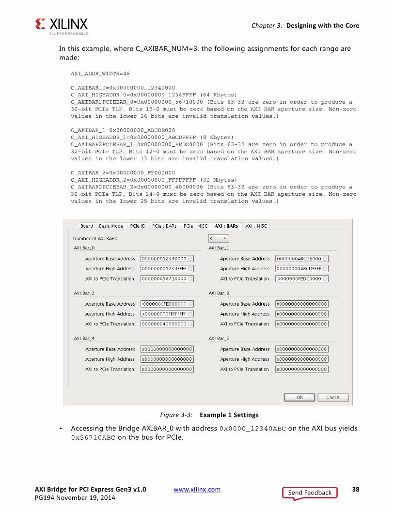
In this example, where C_AXIBAR_NUM=3, the following assignments for each range are made:
AXI_ADDR_WIDTH=48
C_AXIBAR_0=0x00000000_12340000C_AXI_HIGHADDR_0=0x00000000_1234FFFF (64 Kbytes)C_AXIBAR2PCIEBAR_0=0x00000000_56710000 (Bits 63-32 are zero in order to produce a 32-bit PCIe TLP. Bits 15-0 must be zero based on the AXI BAR aperture size. Non-zero values in the lower 16 bits are invalid translation values.)
C_AXIBAR_1=0x00000000_ABCDE000C_AXI_HIGHADDR_1=0x00000000_ABCDFFFF (8 Kbytes)C_AXIBAR2PCIEBAR_1=0x00000000_FEDC0000 (Bits 63-32 are zero in order to produce a 32-bit PCIe TLP. Bits 12-0 must be zero based on the AXI BAR aperture size. Non-zero values in the lower 13 bits are invalid translation values.)
C_AXIBAR_2=0x00000000_FE000000C_AXI_HIGHADDR_2=0x00000000_FFFFFFFF (32 Mbytes)C_AXIBAR2PCIEBAR_2=0x00000000_40000000 (Bits 63-32 are zero in order to produce a 32-bit PCIe TLP. Bits 24-0 must be zero based on the AXI BAR aperture size. Non-zero values in the lower 25 bits are invalid translation values.)
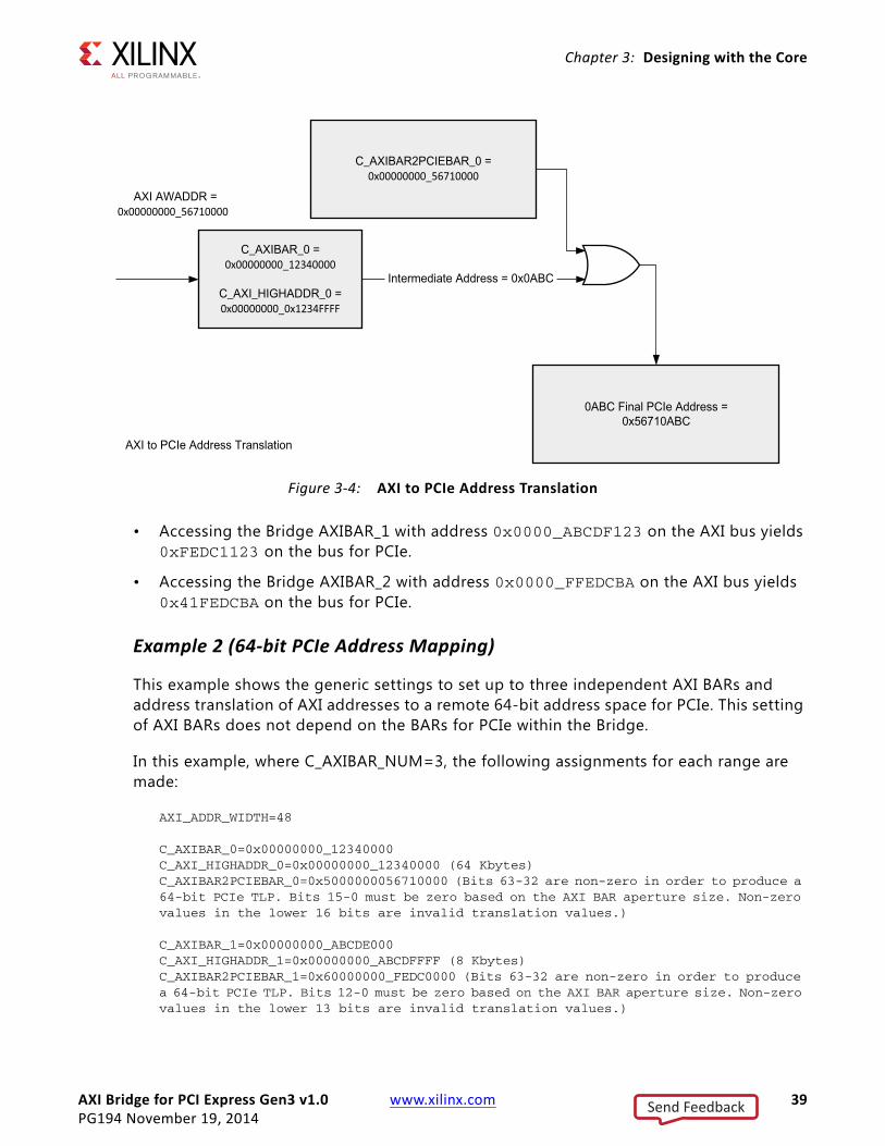
• Accessing the Bridge AXIBAR_0 with address 0x0000_12340ABC on the AXI bus yields 0x56710ABC on the bus for PCIe.
X-Ref Target - Figure 3-3
Figure 3-3: Example 1 Settings
Send Feedback
AXI Bridge for PCI Express Gen3 v1.0 www.xilinx.com 39PG194 November 19, 2014
Chapter 3: Designing with the Core
• Accessing the Bridge AXIBAR_1 with address 0x0000_ABCDF123 on the AXI bus yields 0xFEDC1123 on the bus for PCIe.
• Accessing the Bridge AXIBAR_2 with address 0x0000_FFEDCBA on the AXI bus yields 0x41FEDCBA on the bus for PCIe.
Example 2 (64-bit PCIe Address Mapping)
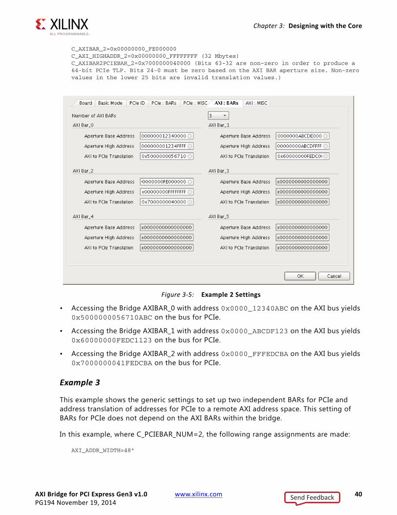
This example shows the generic settings to set up to three independent AXI BARs and address translation of AXI addresses to a remote 64-bit address space for PCIe. This setting of AXI BARs does not depend on the BARs for PCIe within the Bridge.
In this example, where C_AXIBAR_NUM=3, the following assignments for each range are made:
AXI_ADDR_WIDTH=48
C_AXIBAR_0=0x00000000_12340000C_AXI_HIGHADDR_0=0x00000000_12340000 (64 Kbytes)C_AXIBAR2PCIEBAR_0=0x5000000056710000 (Bits 63-32 are non-zero in order to produce a 64-bit PCIe TLP. Bits 15-0 must be zero based on the AXI BAR aperture size. Non-zero values in the lower 16 bits are invalid translation values.)
C_AXIBAR_1=0x00000000_ABCDE000C_AXI_HIGHADDR_1=0x00000000_ABCDFFFF (8 Kbytes)C_AXIBAR2PCIEBAR_1=0x60000000_FEDC0000 (Bits 63-32 are non-zero in order to produce a 64-bit PCIe TLP. Bits 12-0 must be zero based on the AXI BAR aperture size. Non-zero values in the lower 13 bits are invalid translation values.)
X-Ref Target - Figure 3-4
Figure 3-4: AXI to PCIe Address Translation
Send Feedback
AXI Bridge for PCI Express Gen3 v1.0 www.xilinx.com 40PG194 November 19, 2014
Chapter 3: Designing with the Core
C_AXIBAR_2=0x00000000_FE000000C_AXI_HIGHADDR_2=0x00000000_FFFFFFFF (32 Mbytes)C_AXIBAR2PCIEBAR_2=0x7000000040000 (Bits 63-32 are non-zero in order to produce a 64-bit PCIe TLP. Bits 24-0 must be zero based on the AXI BAR aperture size. Non-zero values in the lower 25 bits are invalid translation values.)
• Accessing the Bridge AXIBAR_0 with address 0x0000_12340ABC on the AXI bus yields 0x5000000056710ABC on the bus for PCIe.
• Accessing the Bridge AXIBAR_1 with address 0x0000_ABCDF123 on the AXI bus yields 0x60000000FEDC1123 on the bus for PCIe.
• Accessing the Bridge AXIBAR_2 with address 0x0000_FFFEDCBA on the AXI bus yields 0x7000000041FEDCBA on the bus for PCIe.
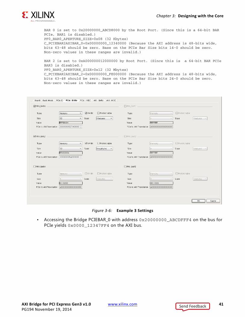
Example 3
This example shows the generic settings to set up two independent BARs for PCIe and address translation of addresses for PCIe to a remote AXI address space. This setting of BARs for PCIe does not depend on the AXI BARs within the bridge.
In this example, where C_PCIEBAR_NUM=2, the following range assignments are made:
AXI_ADDR_WIDTH=48"
X-Ref Target - Figure 3-5
Figure 3-5: Example 2 Settings
Send Feedback
AXI Bridge for PCI Express Gen3 v1.0 www.xilinx.com 41PG194 November 19, 2014
Chapter 3: Designing with the Core
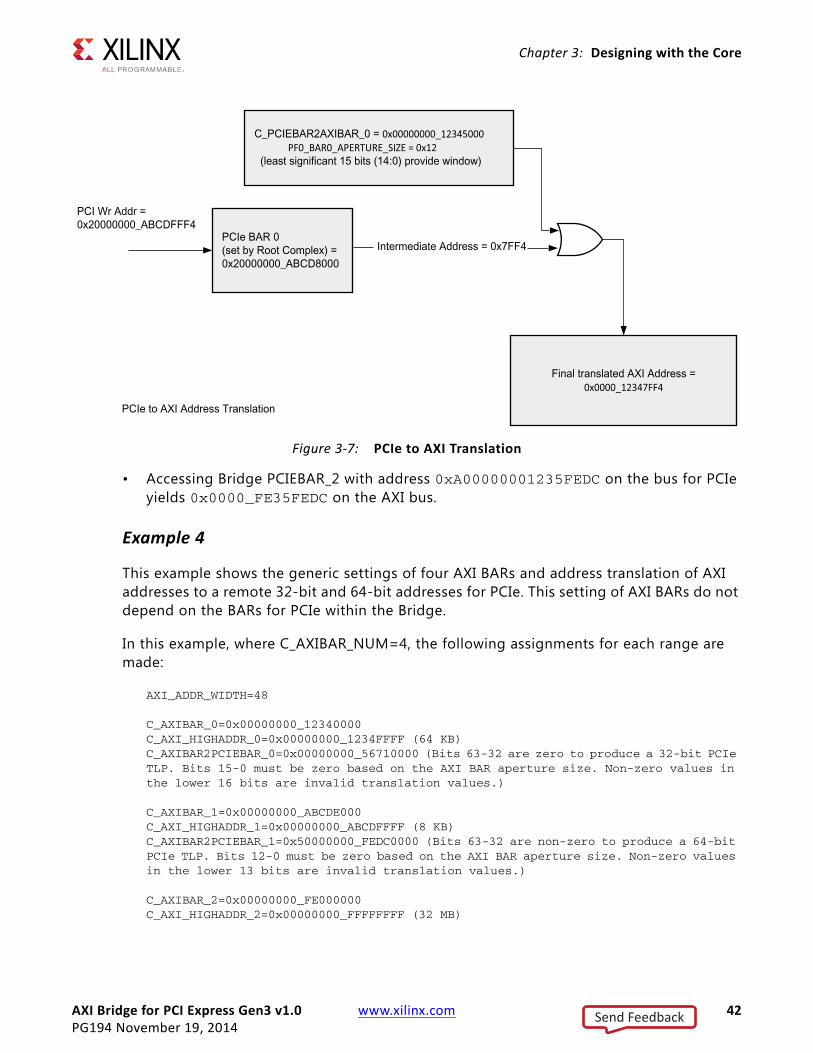
BAR 0 is set to 0x20000000_ABCD8000 by the Root Port. (Since this is a 64-bit BAR PCIe, BAR1 is disabled.)PF0_BAR0_APERTURE_SIZE=0x08 (32 Kbytes)C_PCIEBAR2AXIBAR_0=0x00000000_12340000 (Because the AXI address is 48-bits wide, bits 63-48 should be zero. Base on the PCIe Bar Size bits 14-0 should be zero. Non-zero values in these ranges are invalid.)
BAR 2 is set to 0xA000000012000000 by Root Port. (Since this is a 64-bit BAR PCIe BAR3 is disabled.)PF0_BAR0_APERTURE_SIZE=0x12 (32 Mbytes)C_PCIEBAR2AXIBAR_2=0x00000000_FE000000 (Because the AXI address is 48-bits wide, bits 63-48 should be zero. Base on the PCIe Bar Size bits 24-0 should be zero. Non-zero values in these ranges are invalid.)
• Accessing the Bridge PCIEBAR_0 with address 0x20000000_ABCDFFF4 on the bus for PCIe yields 0x0000_12347FF4 on the AXI bus.
X-Ref Target - Figure 3-6
Figure 3-6: Example 3 Settings
Send Feedback
AXI Bridge for PCI Express Gen3 v1.0 www.xilinx.com 42PG194 November 19, 2014
Chapter 3: Designing with the Core
• Accessing Bridge PCIEBAR_2 with address 0xA00000001235FEDC on the bus for PCIe yields 0x0000_FE35FEDC on the AXI bus.
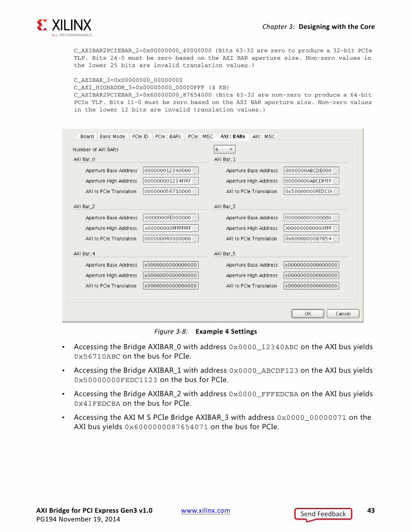
Example 4
This example shows the generic settings of four AXI BARs and address translation of AXI addresses to a remote 32-bit and 64-bit addresses for PCIe. This setting of AXI BARs do not depend on the BARs for PCIe within the Bridge.
In this example, where C_AXIBAR_NUM=4, the following assignments for each range are made:
AXI_ADDR_WIDTH=48
C_AXIBAR_0=0x00000000_12340000C_AXI_HIGHADDR_0=0x00000000_1234FFFF (64 KB)C_AXIBAR2PCIEBAR_0=0x00000000_56710000 (Bits 63-32 are zero to produce a 32-bit PCIe TLP. Bits 15-0 must be zero based on the AXI BAR aperture size. Non-zero values in the lower 16 bits are invalid translation values.)
C_AXIBAR_1=0x00000000_ABCDE000C_AXI_HIGHADDR_1=0x00000000_ABCDFFFF (8 KB)C_AXIBAR2PCIEBAR_1=0x50000000_FEDC0000 (Bits 63-32 are non-zero to produce a 64-bit PCIe TLP. Bits 12-0 must be zero based on the AXI BAR aperture size. Non-zero values in the lower 13 bits are invalid translation values.)
C_AXIBAR_2=0x00000000_FE000000C_AXI_HIGHADDR_2=0x00000000_FFFFFFFF (32 MB)
X-Ref Target - Figure 3-7
Figure 3-7: PCIe to AXI Translation
Send Feedback
AXI Bridge for PCI Express Gen3 v1.0 www.xilinx.com 43PG194 November 19, 2014
Chapter 3: Designing with the Core
C_AXIBAR2PCIEBAR_2=0x00000000_40000000 (Bits 63-32 are zero to produce a 32-bit PCIe TLP. Bits 24-0 must be zero based on the AXI BAR aperture size. Non-zero values in the lower 25 bits are invalid translation values.)
C_AXIBAR_3=0x00000000_00000000C_AXI_HIGHADDR_3=0x00000000_00000FFF (4 KB)C_AXIBAR2PCIEBAR_3=0x60000000_87654000 (Bits 63-32 are non-zero to produce a 64-bit PCIe TLP. Bits 11-0 must be zero based on the AXI BAR aperture size. Non-zero values in the lower 12 bits are invalid translation values.)
• Accessing the Bridge AXIBAR_0 with address 0x0000_12340ABC on the AXI bus yields 0x56710ABC on the bus for PCIe.
• Accessing the Bridge AXIBAR_1 with address 0x0000_ABCDF123 on the AXI bus yields 0x50000000FEDC1123 on the bus for PCIe.
• Accessing the Bridge AXIBAR_2 with address 0x0000_FFFEDCBA on the AXI bus yields 0x41FEDCBA on the bus for PCIe.
• Accessing the AXI M S PCIe Bridge AXIBAR_3 with address 0x0000_00000071 on the AXI bus yields 0x6000000087654071 on the bus for PCIe.
X-Ref Target - Figure 3-8
Figure 3-8: Example 4 Settings
Send Feedback

AXI Bridge for PCI Express Gen3 v1.0 www.xilinx.com 44PG194 November 19, 2014
Chapter 3: Designing with the Core
Addressing Checks
When setting the following parameters for PCIe address mapping, C_PCIE2AXIBAR_n and PF0_BARn_APERTURE_SIZE, be sure these are set to allow for the addressing space on the AXI system. For example, the following setting is illegal and results in an invalid AXI address.
C_PCIE2AXIBAR_0 = 0x00000000_FFFFF000PF0_BARn_APERTURE_SIZE=0x06 (8 KB)
For an 8 Kilobyte BAR the lower 13 bits must be zero. As result, the C_PCIE2AXIBAR_0 value should be modif ied to be 0x00000000_FFFFE0000. Also, check for a larger value on PF0_BARn_APERTURE_SIZE compared to the value assigned to parameter, C_PCIE2AXIBAR_n. For example, the following parameter settings.
C_PCIE2AXIBAR_0 = 0xFFFF_E000PF0_BARn_APERTURE_SIZE=0x0D (1 MB)
To keep the AXIBAR upper address bits as 0xFFFF_E000 (to reference bits [31:13]), the PF0_BARn_APERTURE_SIZE parameter must be set to 0x06 (8 KB).
InterruptsInterrupt capabilities are provided by the underlying PCI Express solution IP. For additional information, see the Virtex-7 FPGAs Gen3 Integrated Block for PCI Express Product Guide (PG023) [Ref 3] and the UltraScale Architecture Gen3 Integrated Block for PCI Express Product Guide (PG156) [Ref 4].
Malformed TLPThe integrated block for PCI Express detects a malformed TLP. For the IP configured as an Endpoint core, a malformed TLP results in a fatal error message being sent upstream if error reporting is enabled in the Device Control Register.
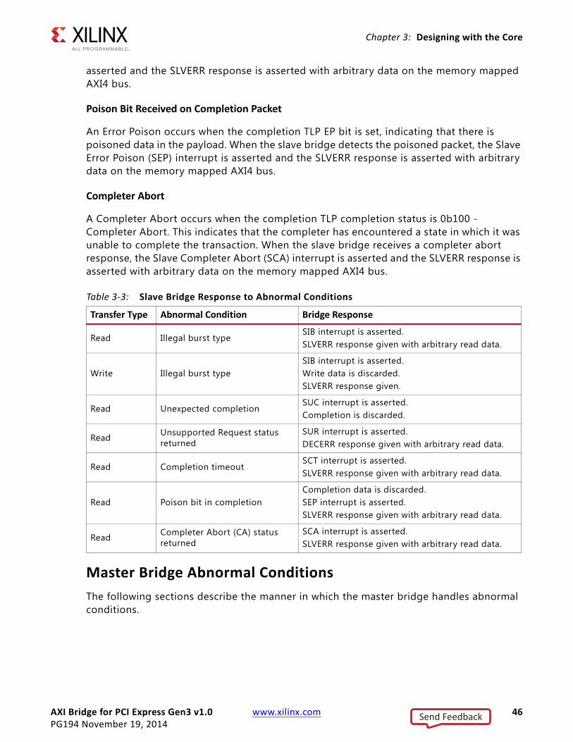
Abnormal ConditionsThis section describes how the Slave side (Table 3-3) and Master side (Table 3-4) of the AXI Bridge for PCI Express Gen3 core handle abnormal conditions.
Send Feedback
AXI Bridge for PCI Express Gen3 v1.0 www.xilinx.com 45PG194 November 19, 2014
Chapter 3: Designing with the Core
Slave Bridge Abnormal ConditionsSlave bridge abnormal conditions are classif ied as: Illegal Burst Type and Completion TLP Errors. The following sections describe the manner in which the Bridge handles these errors.
Illegal Burst Type
The slave bridge monitors AXI read and write burst type inputs to ensure that only the INCR (incrementing burst) type is requested. Any other value on these inputs is treated as an error condition and the Slave Illegal Burst (SIB) interrupt is asserted. In the case of a read request, the Bridge asserts SLVERR for all data beats and arbitrary data is placed on the s_axi_rdata bus. In the case of a write request, the Bridge asserts SLVERR for the write response and all write data is discarded.
Completion TLP Errors
Any request to the bus for PCIe (except for posted Memory write) requires a completion TLP to complete the associated AXI request. The Slave side of the Bridge checks the received completion TLPs for errors and checks for completion TLPs that are never returned (Completion Timeout). Each of the completion TLP error types are discussed in the subsequent sections.
Unexpected Completion
When the slave bridge receives a completion TLP, it matches the header RequesterID and Tag to the outstanding RequesterID and Tag. A match failure indicates the TLP is an Unexpected Completion which results in the completion TLP being discarded and a Slave Unexpected Completion (SUC) interrupt strobe being asserted. Normal operation then continues.
Unsupported Request
A device for PCIe might not be capable of satisfying a specif ic read request. For example, the read request targets an unsupported address for PCIe causing the completer to return a completion TLP with a completion status of 0b001 - Unsupported Request. The completer can also return a completion TLP with a completion status that is reserved according to the 2.1 PCIe Specification, which must be treated as an unsupported request status. When the slave bridge receives an unsupported request response, the Slave Unsupported Request (SUR) interrupt is asserted and the DECERR response is asserted with arbitrary data on the memory mapped AXI4 bus.
Completion Timeout
A Completion Timeout occurs when a completion (Cpl) or completion with data (CplD) TLP is not returned after an AXI to PCIe read request. Completions must complete within the C_COMP_TIMEOUT parameter selected value from the time the MemRd for PCIe request is issued. When a completion timeout occurs, a Slave Completion Timeout (SCT) interrupt is
Send Feedback
AXI Bridge for PCI Express Gen3 v1.0 www.xilinx.com 46PG194 November 19, 2014
Chapter 3: Designing with the Core
asserted and the SLVERR response is asserted with arbitrary data on the memory mapped AXI4 bus.
Poison Bit Received on Completion Packet
An Error Poison occurs when the completion TLP EP bit is set, indicating that there is poisoned data in the payload. When the slave bridge detects the poisoned packet, the Slave Error Poison (SEP) interrupt is asserted and the SLVERR response is asserted with arbitrary data on the memory mapped AXI4 bus.
Completer Abort
A Completer Abort occurs when the completion TLP completion status is 0b100 - Completer Abort. This indicates that the completer has encountered a state in which it was unable to complete the transaction. When the slave bridge receives a completer abort response, the Slave Completer Abort (SCA) interrupt is asserted and the SLVERR response is asserted with arbitrary data on the memory mapped AXI4 bus.
Master Bridge Abnormal ConditionsThe following sections describe the manner in which the master bridge handles abnormal conditions.
Table 3-3: Slave Bridge Response to Abnormal Conditions
Transfer Type Abnormal Condition Bridge Response
Read Illegal burst typeSIB interrupt is asserted.SLVERR response given with arbitrary read data.
Write Illegal burst typeSIB interrupt is asserted.Write data is discarded.SLVERR response given.
Read Unexpected completionSUC interrupt is asserted.Completion is discarded.
Read Unsupported Request status returned
SUR interrupt is asserted.DECERR response given with arbitrary read data.
Read Completion timeoutSCT interrupt is asserted.SLVERR response given with arbitrary read data.
Read Poison bit in completionCompletion data is discarded.SEP interrupt is asserted.SLVERR response given with arbitrary read data.
Read Completer Abort (CA) status returned
SCA interrupt is asserted.SLVERR response given with arbitrary read data.
Send Feedback

AXI Bridge for PCI Express Gen3 v1.0 www.xilinx.com 47PG194 November 19, 2014
Chapter 3: Designing with the Core
AXI DECERR Response
When the master bridge receives a DECERR response from the AXI bus, the request is discarded and the Master DECERR (MDE) interrupt is asserted. If the request was non-posted, a completion packet with the Completion Status = Unsupported Request (UR) is returned on the bus for PCIe.
AXI SLVERR Response
When the master bridge receives a SLVERR response from the addressed AXI slave, the request is discarded and the Master SLVERR (MSE) interrupt is asserted. If the request was non-posted, a completion packet with the Completion Status = Completer Abort (CA) is returned on the bus for PCIe.
Max Payload Size for PCIe, Max Read Request Size or 4K Page Violated
It is the responsibility of the requester to ensure that the outbound request adhere to the Max Payload Size, Max Read Request Size, and 4 Kb Page Violation rules. If the master bridge receives a request that violates one of these rules, the bridge processes the invalid request as a valid request, which can return a completion that violates one of these conditions or can result in the loss of data. The master bridge does not return a malformed TLP completion to signal this violation.
Completion Packets
When the MAX_READ_REQUEST_SIZE is greater than the MAX_PAYLOAD_SIZE, a read request for PCIe can ask for more data than the master bridge can insert into a single completion packet. When this situation occurs, multiple completion packets are generated up to MAX_PAYLOAD_SIZE, with the Read Completion Boundary (RCB) observed.
Poison Bit
When the poison bit is set in a transaction layer packet (TLP) header, the payload following the header is corrupted. When the master bridge receives a memory request TLP with the poison bit set, it discards the TLP and asserts the Master Error Poison (MEP) interrupt strobe.
Zero Length Requests
When the master bridge receives a read request with the Length = 0x1, FirstBE = 0x00, and LastBE = 0x00, it responds by sending a completion with Status = Successful Completion. When the master bridge receives a write request with the Length = 0x1, FirstBE = 0x00, and LastBE = 0x00 there is no effect.
Send Feedback

AXI Bridge for PCI Express Gen3 v1.0 www.xilinx.com 48PG194 November 19, 2014
Chapter 3: Designing with the Core
Link Down BehaviorThe normal operation of the AXI Bridge for PCI Express Gen3 core is dependent on the integrated block for PCIe establishing and maintaining the point-to-point link with an external device for PCIe. If the link has been lost, it must be re-established to return to normal operation.
When a Hot Reset is received by the AXI Bridge for PCI Express Gen3 core, the link goes down and the PCI Configuration Space must be reconfigured.
Initiated AXI4 write transactions that have not yet completed on the AXI4 bus when the link goes down have a SLVERR response given and the write data is discarded. Initiated AXI4 read transactions that have not yet completed on the AXI4 bus when the link goes down have a SLVERR response given, with arbitrary read data returned.
Any MemWr TLPs for PCIe that have been received, but the associated AXI4 write transaction has not started when the link goes down, are discarded. If the associated AXI4 write transaction is in the process of being transferred, it completes as normal. Any MemRd TLPs for PCIe that have been received, but have not returned completion TLPs by the time the link goes down, complete on the AXI4 bus, but do not return completion TLPs on the PCIe bus.
Table 3-4: Master Bridge Response to Abnormal Conditions
Transfer Type Abnormal Condition Bridge Response
Read DECERR responseMDE interrupt strobe asserted.Completion returned with Unsupported Request status.
Write DECERR response MDE interrupt strobe asserted.
Read SLVERR responseMSE interrupt strobe asserted.Completion returned with Completer Abort status.
Write SLVERR response MSE interrupt strobe asserted.
Write Poison bit set in requestMEP interrupt strobe asserted.Data is discarded.
Read DECERR responseMDE interrupt strobe asserted.Completion returned with Unsupported Request status.
Write DECERR response MDE interrupt strobe asserted.
Send Feedback

AXI Bridge for PCI Express Gen3 v1.0 www.xilinx.com 49PG194 November 19, 2014
Chapter 4
Design Flow StepsThis chapter describes customizing and generating the core, constraining the core, and the simulation, synthesis and implementation steps that are specific to this IP core. More detailed information about the standard design flows in the Vivado® IP Integrator can be found in the following Vivado Design Suite user guides:
• Vivado Design Suite User Guide: Designing IP Subsystems using IP Integrator (UG994) [Ref 14]
• Vivado Design Suite User Guide: Designing with IP (UG896) [Ref 11]
• Vivado Design Suite User Guide: Getting Started (UG910) [Ref 10]
• Vivado Design Suite User Guide: Logic Simulation (UG900) [Ref 12]
Customizing and Generating the CoreThis section includes information about using the Vivado Design Suite to customize and generate the core.
Note: If you are customizing and generating the core in the Vivado IP Integrator, see the Vivado Design Suite User Guide: Designing IP Subsystems using IP Integrator (UG994) [Ref 14] for detailed information. IP Integrator might auto-compute certain configuration values when validating or generating the design. To check whether the values do change, see the description of the parameter in this chapter. To view the parameter value you can run the validate_bd_design command in the Tcl Console.
You can customize the IP for use in your design by specifying values for the various parameters associated with the IP core using the following steps:
1. Select the IP from the IP catalog.
2. Double-click the selected IP, or select the Customize IP command from the toolbar or right-click menu.
Send Feedback

AXI Bridge for PCI Express Gen3 v1.0 www.xilinx.com 50PG194 November 19, 2014
Chapter 4: Design Flow Steps
For details, see the Vivado Design Suite User Guide: Designing with IP (UG896) [Ref 11] and the Vivado Design Suite User Guide: Getting Started (UG910) [Ref 10].
Note: Figures in this chapter are illustrations of the Vivado Integrated Design Environment (IDE). This layout might vary from the current version.
Customizing the Core The AXI Bridge for PCI Express Gen3 core customization parameters are described in the following sections.
Basics Parameter Settings
The initial customization screen shown in Figure 4-1 is used to define the basic parameters for the core, including the component name, PCIe configuration, AXI parameters, and reference clock. Figure 4-2 and Figure 4-3 show the parameters available for the Advanced Mode.
Note: In the Basic Mode tab, the addition parameters available in Advanced Mode are applicable to UltraScale architecture devices only.
X-Ref Target - Figure 4-1
Figure 4-1: Basics Parameter Settings: Basic Mode Selected
Send Feedback

AXI Bridge for PCI Express Gen3 v1.0 www.xilinx.com 51PG194 November 19, 2014
Chapter 4: Design Flow Steps
Component Name
Base name of the output f iles generated for the core. The name must begin with a letter and can be composed of these characters: a to z, 0 to 9, and “_.”
Mode
Allows you to select the Basic or Advanced mode of the configuration of core.
Device / Port Type
Indicates the PCI Express logical device type.
PCIe Block Location
Selects from the available integrated blocks to enable generation of location-specif ic constraint f iles and pinouts. This selection is used in the default example design scripts.
X-Ref Target - Figure 4-2
Figure 4-2: Basic Parameter Settings: Advanced Mode Selected
X-Ref Target - Figure 4-3
Figure 4-3: Additional Basic Parameter Settings: Advanced Mode Selected
Send Feedback

AXI Bridge for PCI Express Gen3 v1.0 www.xilinx.com 52PG194 November 19, 2014
Chapter 4: Design Flow Steps
Enable GT Quad Selection
This parameter is used to enable the device/package migration. Applicable to UltraScale devices only.
Number of Lanes
The core requires the selection of the initial lane width. Wider lane width cores can train down to smaller lane widths and consume more FPGA resource.
Maximum Link Speed
Indicates the maximum link speed supported by the design. Higher link speed cores are capable of training to lower link speeds and run at a higher clock frequency.
AXI Address Width
Indicates the AXI address width for the S_AXI and M_AXI interfaces, but does not affect the address width of the S_AXI_CTL interface.
AXI Data Width
Indicates the AXI data width for the S_AXI and M_AXI interfaces, but does not affect the data width of the S_AXI_CTL interface.
AXI Clock Frequency
Indicates the clock frequency that will be generated on the axi_aclk output. All AXI interfaces and a majority of the core outputs are synchronous to this clock.
Enable AXI Slave Interface
Allows the slave bridge to be enabled or disabled as desired by the system design. If only the master bridge is used the slave bridge can be disabled to conserve FPGA resources.
Enable AXI Master Interface
Allows the master bridge to be enabled or disabled as desired by the system design. If only the slave bridge is used, the master bridge can be disabled to conserve FPGA resources.
Reference Clock Frequency
Selects the frequency of the reference clock provided on the refclk input.
Enable Pipe Simulation
When selected, this option generates the core that can be simulated with PIPE interfaces connected.
Send Feedback
AXI Bridge for PCI Express Gen3 v1.0 www.xilinx.com 53PG194 November 19, 2014
Chapter 4: Design Flow Steps
Enable GT Channel DRP Ports
When checked, enables the GT channel DRP interface.
Enable PCIe DRP Ports
When checked, enables the PCIe DRP interface.
Tandem Mode
For supported devices only, this option allow you to choose the Tandem Configuration mode: None, Tandem PROM and Tandem PCIe.
Enable External STARTUP primitive
When checked, generates the STARTUP primitive external to the IP.
Use the dedicated PERST routing resources
Enables sys_rst dedicated routing for the PCIE_X0Y0 block.
System Reset polarity
This parameter is used to set the polarity of the sys_rst ACTIVE_HIGH or ACTIVE_LOW.
PCIe ID Settings
The Identity Settings pages are shown in Figure 4-4. These settings customize the IP initial values and device class code.
Send Feedback
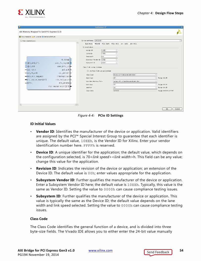
AXI Bridge for PCI Express Gen3 v1.0 www.xilinx.com 54PG194 November 19, 2014
Chapter 4: Design Flow Steps
ID Initial Values
• Vendor ID: Identif ies the manufacturer of the device or application. Valid identif iers are assigned by the PCI™ Special Interest Group to guarantee that each identif ier is unique. The default value, 10EEh, is the Vendor ID for Xilinx. Enter your vendor identif ication number here. FFFFh is reserved.
• Device ID: A unique identif ier for the application; the default value, which depends on the configuration selected, is 70<link speed><link width>h. This f ield can be any value; change this value for the application.
• Revision ID: Indicates the revision of the device or application; an extension of the Device ID. The default value is 00h; enter values appropriate for the application.
• Subsystem Vendor ID: Further qualif ies the manufacturer of the device or application. Enter a Subsystem Vendor ID here; the default value is 10EEh. Typically, this value is the same as Vendor ID. Setting the value to 0000h can cause compliance testing issues.
• Subsystem ID: Further qualif ies the manufacturer of the device or application. This value is typically the same as the Device ID; the default value depends on the lane width and link speed selected. Setting the value to 0000h can cause compliance testing issues.
Class Code
The Class Code identif ies the general function of a device, and is divided into three byte-size f ields. The Vivado IDE allows you to either enter the 24-bit value manually
X-Ref Target - Figure 4-4
Figure 4-4: PCIe ID Settings
Send Feedback

AXI Bridge for PCI Express Gen3 v1.0 www.xilinx.com 55PG194 November 19, 2014
Chapter 4: Design Flow Steps
(default) by either selecting the Enter Class Code Manually checkbox or using the Class Code lookup assistant to populate the f ield. De-select the checkbox to enable the Class Code assistant.
• Base Class: Broadly identif ies the type of function performed by the device.
• Sub-Class: More specif ically identif ies the device function.
• Interface: Defines a specific register-level programming interface, if any, allowing device-independent software to interface with the device.
Class code encoding can be found in the PCI-SIG® specif ications [Ref 7].
Class Code Look-up Assistant
The Class Code Look-up Assistant provides the Base Class, Sub-Class and Interface values for a selected general function of a device. This Look-up Assistant tool only displays the three values for a selected function. You must enter the values in Class Code for these values to be translated into device settings.
PCIe Base Address Registers
The PCIe Base Address Registers (BARs) screen shown in Figure 4-5 set the base address register space for the Endpoint configuration. Each BAR (0 through 5) configures the BAR Aperture Size and Control attributes of the Physical Function, as described in Table 4-1.
X-Ref Target - Figure 4-5
Figure 4-5: PCIe Base Address Register
Send Feedback

AXI Bridge for PCI Express Gen3 v1.0 www.xilinx.com 56PG194 November 19, 2014
Chapter 4: Design Flow Steps
Base Address Register Overview
The AXI Bridge for PCI Express Gen3 core in Endpoint configuration supports up to six 32-bit BARs or three 64-bit BARs.
BARs can be one of two sizes. BARs 0, 2, and 4 can be either 32-bit or 64-bit addressable. BARs 1, 3, and 5 can only be 32-bit addressable and are disabled if the previous BAR is enabled as 64-bit.
• 32-bit BARs: The address space can be as small as 4 kilobytes or as large as 2 gigabytes. Used for Memory to I/O.
• 64-bit BARs: The address space can be as small as 4 kilobytes or as large as 256 gigabytes. Used for Memory only.
Send Feedback
AXI Bridge for PCI Express Gen3 v1.0 www.xilinx.com 57PG194 November 19, 2014
Chapter 4: Design Flow Steps
All BAR registers share these options:
• Checkbox: Click the checkbox to enable the BAR; deselect the checkbox to disable the BAR.
• Type: BARs can be Memory apertures only.
° Memory: Memory BARs can be either 64-bit or 32-bit. Prefetch is enabled for 64-bit and not enabled for 32-bit. When a BAR is set as 64 bits, it uses the next BAR for the extended address space, making it inaccessible.
• Size: The available Size range depends on the PCIe® Device/Port Type and the Type of BAR selected. Table 4-1 lists the available BAR size ranges.
• Prefetchable: Identif ies the ability of the memory space to be prefetched. This can only be enabled for 64-bit addressable bars.
• Value: The value assigned to the BAR based on the current selections.
• PCIe to AXI Translation: This text f ield should be set to the appropriate value to perform the translation from the PCI Express base address to the desired AXI Base Address.
For more information about managing the Base Address Register settings, see Managing Base Address Register Settings.
Managing Base Address Register Settings
Memory indicates that the address space is defined as memory aperture. The base address register only responds to commands that access the specif ied address space.
Disabling Unused Resources
For best results, disable unused base address registers to conserve system resources. A base address register is disabled by deselecting unused BARs in the Vivado IDE.
PCIe Miscellaneous
The PCIe Misc screen is shown in Figure 4-6.
Table 4-1: BAR Size Ranges for Device Configuration
PCIe Device/Port Type BAR Type BAR Size Range
PCI Express Endpoint32-bit Memory 4 Kilobytes - 2 Gigabytes
64-bit Memory 4 Kilobytes - 2 Gigabytes
Send Feedback

AXI Bridge for PCI Express Gen3 v1.0 www.xilinx.com 58PG194 November 19, 2014
Chapter 4: Design Flow Steps
Legacy Interrupt Settings
Indicates the usage of Legacy interrupts.The AXI Bridge for PCI Express Gen3 core implements INTA only.
Enable MSI Capability Structure
Indicates that the MSI capability structure exists.
Multiple Message Capable
Indicates the number of message signals interrupt vectors that this endpoint could request.
Completion Timeout Configuration
Indicates the completion timeout value for incoming completions due to outstanding memory read requests.
X-Ref Target - Figure 4-6
Figure 4-6: PCIe Miscellaneous Setting
Send Feedback

AXI Bridge for PCI Express Gen3 v1.0 www.xilinx.com 59PG194 November 19, 2014
Chapter 4: Design Flow Steps
AXI Base Address Registers
The AXI Base Address Registers (BARs) screen shown in Figure 4-7 sets the AXI base address registers and the translation between AXI Memory space and PCI Express Memory space. Each BAR has a Base Address, High Address, and translation f ield which can be configured through the Vivado IDE.
Number of BARs
Indicates the number of AXI BARs enabled. The BARs are enabled sequentially.
Aperture Base Address
Sets the base address for the address range associated to the BAR. You should edit this parameter to fit design requirements.
Aperture High Address
Sets the upper address threshold for the address range associated to the BAR. You should edit this parameter to f it design requirements.
AXI to PCIe Translation
Configures the translation mapping between AXI and PCI Express address space. You should edit this parameter to f it design requirements.
X-Ref Target - Figure 4-7
Figure 4-7: AXI Base Address Registers
Send Feedback

AXI Bridge for PCI Express Gen3 v1.0 www.xilinx.com 60PG194 November 19, 2014
Chapter 4: Design Flow Steps
AXI Miscellaneous
The AXI Misc screen shown in Figure 4-8 sets the additional AXI parameters.
S AXI ID WIDTH
Sets the ID width for the AXI Slave Interface.
Note: Multiple IDs are not supported for AXI Master Interface. Therefore, all signals concerned with ID are not available at AXI Master Interface.
AXI Master outstanding write transactions
Indicates the number of outstanding write transactions that are allowable for the AXI Master interface.
AXI Master outstanding read transactions
Indicates the number of outstanding read transactions that are allowable for the AXI Master interface.
X-Ref Target - Figure 4-8
Figure 4-8: AXI Misc Settings
Send Feedback
AXI Bridge for PCI Express Gen3 v1.0 www.xilinx.com 61PG194 November 19, 2014
Chapter 4: Design Flow Steps
AXI Slave outstanding write transactions
Indicates the number of outstanding write transactions that are allowable for the AXI Slave interface.
AXI Slave outstanding read transactions
Indicates the number of outstanding read transactions that are allowable for the AXI Slave interface.
Output GenerationFor details, see the Vivado Design Suite User Guide: Designing with IP (UG896) [Ref 11].
For information regarding the example design, see Example Design Output Structure in Chapter 5.
Constraining the CoreThis section contains information about constraining the core in the Vivado Design Suite.
Required ConstraintsThe AXI Bridge for PCI Express Gen3® core requires a clock period constraint for the REFCLK input that agrees with the C_REF_CLK_FREQ parameter setting. In addition, pin-placement (LOC) constraints are needed that are board/part/package specif ic.
See Placement Constraints for more details on the constraint paths for FPGA architectures.
Additional information on clocking can be found in the Xilinx Solution Center for PCI Express (see Solution Centers, page 71).
System IntegrationA typical embedded system including the AXI Bridge for PCI Express Gen3 core is shown in Figure 2-1. Some additional components to this system in the Vivado IP integrator can include the need to connect the MicroBlaze™ processor or Zynq® device ARM® processor peripheral to communicate with PCI Express™ (in addition to the AXI4-Lite register port on the PCIe bridge). The AXI Interconnect provides this capability and performs the necessarily conversions for the various AXI ports that might be connected to the AXI Interconnect IP (described in [Ref 8]).
The AXI Bridge for PCI Express Gen3 core can be configured with each port connection for an AXI Vivado IP integrator system topology. When instantiating the core, ensure the following bus interface tags are defined.
Send Feedback
AXI Bridge for PCI Express Gen3 v1.0 www.xilinx.com 62PG194 November 19, 2014
Chapter 4: Design Flow Steps
BUS_INTERFACE M_AXIBUS_INTERFACE S_AXIBUS_INTERFACE S_AXI_CTL
PCIe Clock Integration
The PCIe differential clock input in the system might need to use a differential input buffer (that is instantiated separately) from the AXI Bridge for the PCIe core. The Vivado IP integrator automatically inserts the appropriate clock buffer.
Placement ConstraintsThe AXI Bridge for PCI Express Gen3 core provides a Xilinx design constraint (XDC) file for all supported PCIe, Part, and Package permutations. You can find the generated XDC file in the Sources tab of the Vivado IDE after generating the IP in the Customize IP dialog box.
For design platforms, it might be necessary to manually place and constrain the underlying blocks of the AXI Bridge for the PCIe core. The modules to assign a LOC constraint include:
• the embedded integrated block for PCIe itself
• the GTH transceivers (for each channel)
• the PCIe differential clock input (if utilized)
The following subsection describes the example location constraints.
Location Constraints
This section highlights the LOC constraints to be specified in the XDC file for the AXI Bridge for PCI Express Gen3 core for design implementations.
For placement/path information on the integrated block for PCIe itself, the following constraint can be utilized:
# 7-Series Constraintset_property LOC PCIE_X*Y* [get_cells {axi_pcie3_0_i/inst/pcie3_ip_i/inst/pcie_top_i/pcie_7vx_i/PCIE_3_0_i}]# Ultrascale Constraintset_property LOC PCIE_X*Y* [get_cells {axi_pcie3_0_i/inst/pcie3_ip_i/inst/pcie3_uscale_top_inst/pcie3_uscale_wrapper_inst/PCIE_3_1_inst}]
For placement/path information of the GTX transceivers, the following constraint can be utilized:
# 7-Series Constraintset_property LOC GTXE2_CHANNEL_X*Y* [get_cells {axi_pcie3_0_i/inst/pcie3_ip_i/inst/gt_top_i/pipe_wrapper_i/pipe_lane[0].gt_wrapper_i/gth_channel.gthe2_channel_i}]# Ultrascale Constraintset_property LOC GTXE2_CHANNEL_X*Y* [get_cells {axi_pcie3_0_i/inst/pcie3_ip_i/inst/gt_top_i/gt_wizard.gtwizard_top_i/axi_pcie3_0_pcie3_ip_gt_i/inst/gen_gtwizard_gthe3_top.axi_pcie3_0_pcie3_ip_gt_gtwizard_gthe3_inst/
Send Feedback

AXI Bridge for PCI Express Gen3 v1.0 www.xilinx.com 63PG194 November 19, 2014
Chapter 4: Design Flow Steps
gen_gtwizard_gthe3.gen_channel_container[1].gen_enabled_channel.gthe3_channel_wrapper_inst/channel_inst/gthe3_channel_gen.gen_gthe3_channel_inst[0].GTHE3_CHANNEL_PRIM_INST}]
For placement/path constraints of the input PCIe differential clock source (using the example provided in System Integration), the following can be utilized:
set_property LOC IBUFDS_GTE2_X*Y* [get_cells {refclk_ibuf}]
Clock FrequenciesThe AXI Memory Mapped to PCI Express Bridge supports reference clock frequencies of 100 MHz, 125 MHz, and 250 MHz and is configurable within the Vivado IDE.
Clock ManagementFor details, see Clocking in Chapter 3.
Clock PlacementFor details, see Placement Constraints.
BankingThis section is not applicable for this IP core.
Transceiver PlacementThe Transceiver primitives adjacent to the PCIe hard block should be used to aid in the place and route of the solution IP. The adjacent Transceiver banks one above or one below the desired PCIe hard block can also be used. Transceivers outside this range are not likely to meet the timing requirements for the PCI Express Solution IP and should not be used.
I/O Standard and PlacementThe sys_reset_n input should be driven directly by FPGA I/O pins. The pin should be driven by the PCI Express edge connector reset signal (perstn). As described in the PCI Express specification, the PCI Express edge connector reset is driven at 3.3V. If the bank voltage for the sys_reset_n pin differs from 3.3V, and external level shifter is required to convert the 3.3V PCI Express edge connector reset (perstn) to the desired FPGA bank voltage.
Send Feedback
AXI Bridge for PCI Express Gen3 v1.0 www.xilinx.com 64PG194 November 19, 2014
Chapter 4: Design Flow Steps
Simulation• For comprehensive information about Vivado simulation components, as well as
information about using supported third party tools, see the Vivado Design Suite User Guide: Logic Simulation (UG900) [Ref 12].
• For information regarding simulating the example design, see Simulation Design Overview in Chapter 5.
Synthesis and Implementation• For details about synthesis and implementation, see the Vivado Design Suite User
Guide: Designing with IP (UG896) [Ref 11].
• For information regarding implementing the example design, see Implementation Design Overview in Chapter 5.
Send Feedback

AXI Bridge for PCI Express Gen3 v1.0 www.xilinx.com 65PG194 November 19, 2014
Chapter 5
Example DesignThis chapter contains information about the example design provided in the Vivado® Design Suite.
OverviewThe example simulation design for the Endpoint configuration of the AXI-PCIe block consists of two parts.
• Root Port Model: a test bench that generates, consumes, and checks PCI Express bus traffic
• AXI BRAM Controller
Simulation Design OverviewFor the simulation design, transactions are sent from the Root Port Model to the AXI Bridge for PCI Express Gen3 core configured as an Endpoint and processed inside the AXI BRAM controller design.
Figure 5-1 illustrates the simulation design provided with the AXI Bridge for PCI Express Gen3 core.
Send Feedback
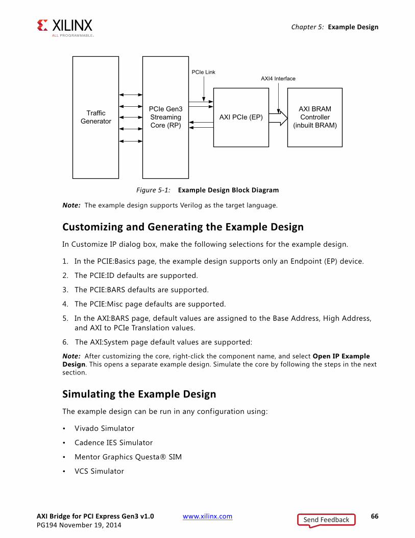
AXI Bridge for PCI Express Gen3 v1.0 www.xilinx.com 66PG194 November 19, 2014
Chapter 5: Example Design
Note: The example design supports Verilog as the target language.
Customizing and Generating the Example DesignIn Customize IP dialog box, make the following selections for the example design.
1. In the PCIE:Basics page, the example design supports only an Endpoint (EP) device.
2. The PCIE:ID defaults are supported.
3. The PCIE:BARS defaults are supported.
4. The PCIE:Misc page defaults are supported.
5. In the AXI:BARS page, default values are assigned to the Base Address, High Address, and AXI to PCIe Translation values.
6. The AXI:System page default values are supported:
Note: After customizing the core, right-click the component name, and select Open IP Example Design. This opens a separate example design. Simulate the core by following the steps in the next section.
Simulating the Example DesignThe example design can be run in any configuration using:
• Vivado Simulator
• Cadence IES Simulator
• Mentor Graphics Questa® SIM
• VCS Simulator
X-Ref Target - Figure 5-1
Figure 5-1: Example Design Block Diagram
Send Feedback

AXI Bridge for PCI Express Gen3 v1.0 www.xilinx.com 67PG194 November 19, 2014
Chapter 5: Example Design
Vivado Simulator
By defaults, the simulator is set to Vivado simulator. To run a simulation, click Run Behavioral Simulation in the Flow Navigator.
Cadence IES
For a Cadence IES simulation, the following steps are required:
1. In Vivado IDE, change the simulation settings as follows:
° Target simulator: Incisive Enterprise Simulator (IES)
2. On the simulator tab, select Run Simulation > Run behavioral simulation.
Mentor Graphics Questa SIM
For a Questa SIM simulation, the following steps are required:
1. In the Vivado IDE, change the simulation settings as follows:
° Target simulator: QuestaSim/ModelSim
2. On the Simulator tab, select Run Simulation > Run behavioral simulation.
IMPORTANT: Due to a bug with the Questa SIM version provided with the current Vivado Design Suite, simulation fails with a SIGABRT error. To resolve the issue, use Questa SIM 10.3c_1 instead.
VCS Simulator
For a VCS simulation, the following steps are required:
1. In Vivado IDE, change the simulation settings as follows:
° Target simulator: Verilog Compiler Simulator (VCS)
2. On the simulator tab, select Run Simulation > Run behavioral simulation.
Implementation Design OverviewFor implementation design, the AXI-BRAM controller can be used as a scratch pad memory to write and read to Block RAM locations.
Send Feedback

AXI Bridge for PCI Express Gen3 v1.0 www.xilinx.com 68PG194 November 19, 2014
Chapter 5: Example Design
Example Design ElementsThe core wrapper includes:
• An example Verilog HDL or VHDL wrapper (instantiates the cores and example design).
• A customizable demonstration test bench to simulate the example design.
Example Design Output StructureFigure 5-2 provides the output structure of the example design.
Table 5-1 provides a descriptions of the contents of the example design directories.
Table 5-1: Example Design Structure
X-Ref Target - Figure 5-2
Figure 5-2: Example Design Output Structure
Directory Description
project_1/axi_pcie3_example Contains all example design f iles.
project_1/axi_pcie3_example/axi_pcie3_example.srcs/sources_1/imports/example_design/
Contains the top module for the example design, xilinx_axi_pcie3_ep.v.
Send Feedback
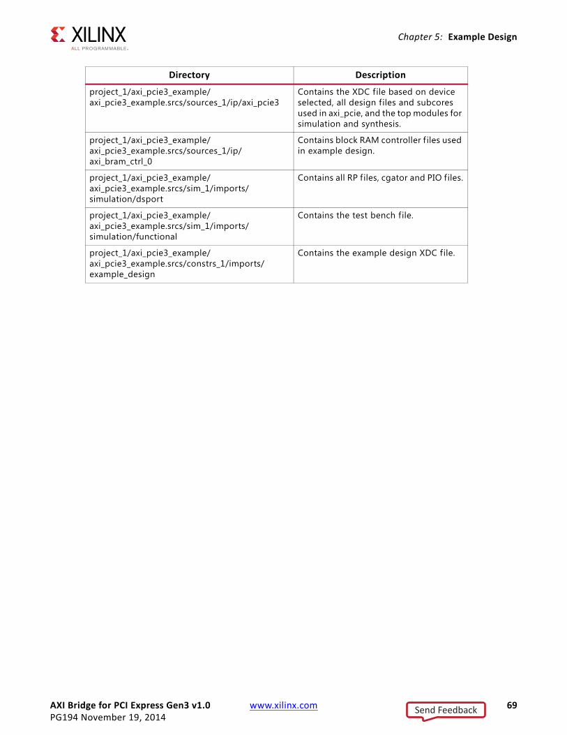
AXI Bridge for PCI Express Gen3 v1.0 www.xilinx.com 69PG194 November 19, 2014
Chapter 5: Example Design
project_1/axi_pcie3_example/axi_pcie3_example.srcs/sources_1/ip/axi_pcie3
Contains the XDC file based on device selected, all design files and subcores used in axi_pcie, and the top modules for simulation and synthesis.
project_1/axi_pcie3_example/axi_pcie3_example.srcs/sources_1/ip/axi_bram_ctrl_0
Contains block RAM controller f iles used in example design.
project_1/axi_pcie3_example/axi_pcie3_example.srcs/sim_1/imports/simulation/dsport
Contains all RP files, cgator and PIO files.
project_1/axi_pcie3_example/axi_pcie3_example.srcs/sim_1/imports/simulation/functional
Contains the test bench file.
project_1/axi_pcie3_example/axi_pcie3_example.srcs/constrs_1/imports/example_design
Contains the example design XDC file.
Directory Description
Send Feedback

AXI Bridge for PCI Express Gen3 v1.0 www.xilinx.com 70PG194 November 19, 2014
Chapter 6
Test BenchFor information about the test bench for the example design, see Chapter 5, Example Design.
Send Feedback

AXI Bridge for PCI Express Gen3 v1.0 www.xilinx.com 71PG194 November 19, 2014
Appendix A
DebuggingThis appendix provides information for using the resources available on the Xilinx® Support website, debug tools, and other step-by-step processes for debugging designs that use the AXI Bridge for PCI Express Gen3 core.
Finding Help on Xilinx.comTo help in the design and debug process when using the AXI Bridge for PCI Express Gen3 core, the Xilinx Support web page (www.xilinx.com/support) contains key resources such as product documentation, release notes, answer records, information about known issues, and links for opening a Technical Support WebCase.
DocumentationThis product puide is the main document associated with the AXI Bridge for PCI Express Gen3 core. This guide, along with documentation related to all products that aid in the design process, can be found on the Xilinx Support web page (www.xilinx.com/support) or by using the Xilinx Documentation Navigator.
You can download the Xilinx Documentation Navigator from the Design Tools tab on the Downloads page (www.xilinx.com/download). For more information about this tool and the features available, see the online help after installation.
Solution CentersSee the Xilinx Solution Centers for support on devices, software tools, and intellectual property at all stages of the design cycle. Topics include design assistance, advisories, and troubleshooting tips.
The PCI Express Solution Center is located at Xilinx Solution Center for PCI Express. Extensive debugging collateral is available in AR: 56802.
Answer RecordsAnswer Records include information about commonly encountered problems, helpful information on how to resolve these problems, and any known issues with a Xilinx product.
Send Feedback

AXI Bridge for PCI Express Gen3 v1.0 www.xilinx.com 72PG194 November 19, 2014
Appendix A: Debugging
Answer Records are created and maintained daily ensuring that users have access to the most accurate information available.
Answer Records for this core are listed below, and can be located by using the Search Support box on the main Xilinx support web page. To maximize your search results, use proper keywords, such as:
• the product name
• tool messages
• summary of the issue encountered
A filter search is available after results are returned to further target the results.
Master Answer Record for the AXI Bridge for PCI Express Gen3
AR: 61898
Contacting Technical SupportXilinx provides technical support at www.xilinx.com/support for this product when used as described in the product documentation. Xilinx cannot guarantee timing, functionality, or support of product if implemented in devices that are not defined in the documentation, if customized beyond that allowed in the product documentation, or if changes are made to any section of the design labeled DO NOT MODIFY.
To contact Xilinx Technical Support:
1. Navigate to www.xilinx.com/support.
2. Open a WebCase by selecting the WebCase link located under Support Quick Links.
When opening a WebCase, include:
• Target FPGA including package and speed grade.
• All applicable Xilinx Design Tools and simulator software versions.
• Additional f iles based on the specif ic issue might also be required. See the relevant sections in this debug guide for guidelines about which f iles to include with the WebCase.
Note: Access to WebCase is not available in all cases. Log in to the WebCase tool to see your specif ic support options.
Send Feedback

AXI Bridge for PCI Express Gen3 v1.0 www.xilinx.com 73PG194 November 19, 2014
Appendix A: Debugging
Debug ToolsThere are many tools available to address AXI Bridge for PCI Express Gen3 design issues. It is important to know which tools are useful for debugging various situations.
Vivado Lab ToolVivado® lab tools inserts logic analyzer (ILA) and virtual I/O (VIO) cores directly into your design. Vivado lab tools also allow you to set trigger conditions to capture application and integrated block port signals in hardware. Captured signals can then be analyzed. This feature in the Vivado IDE is used for logic debugging and validation of a design running in Xilinx devices.
The Vivado logic analyzer is used to interact with the logic debug cores, including:
• ILA 2.0 (and later versions)
• VIO 2.0 (and later versions)
See Vivado Design Suite User Guide: Programming and Debugging (UG908) [Ref 13].
Reference BoardsVarious Xilinx development boards support the AXI Bridge for PCI Express Gen3 core. These boards can be used to prototype designs and establish that the core can communicate with the system.
• 7 series evaluation boards
° VC709
Send Feedback

AXI Bridge for PCI Express Gen3 v1.0 www.xilinx.com 74PG194 November 19, 2014
Appendix A: Debugging
Third-Party ToolsThis section describes third-party software tools that can be useful in debugging.
LSPCI (Linux)
LSPCI is available on Linux platforms and allows you to view the PCI Express device configuration space. LSPCI is usually found in the /sbin directory. LSPCI displays a list of devices on the PCI buses in the system. See the LSPCI manual for all command options. Some useful commands for debugging include:
• lspci -x -d [<vendor>]:[<device>]
This displays the f irst 64 bytes of configuration space in hexadecimal form for the device with vendor and device ID specif ied (omit the -d option to display information for all devices). The default Vendor/Device ID for Xilinx cores is 10EE:6012. Here is a sample of a read of the configuration space of a Xilinx device:
> lspci -x -d 10EE:601281:00.0 Memory controller: Xilinx Corporation: Unknown device 601200: ee 10 12 60 07 00 10 00 00 00 80 05 10 00 00 0010: 00 00 80 fa 00 00 00 00 00 00 00 00 00 00 00 0020: 00 00 00 00 00 00 00 00 00 00 00 00 ee 10 6f 5030: 00 00 00 00 40 00 00 00 00 00 00 00 05 01 00 00
Included in this section of the configuration space are the Device ID, Vendor ID, Class Code, Status and Command, and Base Address Registers.
• lspci -xxxx -d [<vendor>]:[<device>]
This displays the extended configuration space of the device. It can be useful to read the extended configuration space on the root and look for the Advanced Error Reporting (AER) registers. These registers provide more information on why the device has flagged an error (for example, it might show that a correctable error was issued because of a replay timer timeout).
• lspci -k
Shows kernel drivers handling each device and kernel modules capable of handling it (works with kernel 2.6 or later).
PCItree (Windows)
PCItree can be downloaded at www.pcitree.de and allows you to view the PCI Express device configuration space and perform one DWORD memory writes and reads to the aperture.
The configuration space is displayed by default in the lower right corner when the device is selected, as shown in Figure A-1.
Send Feedback
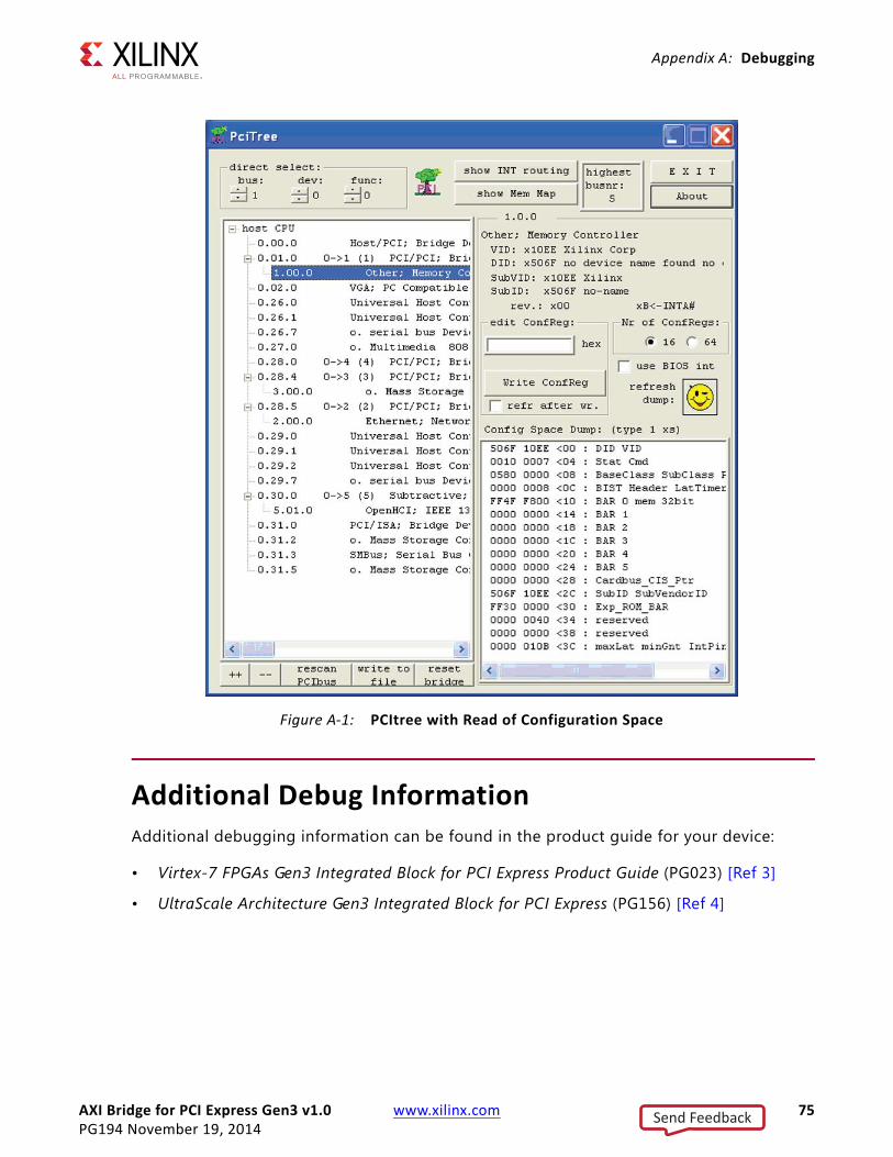
AXI Bridge for PCI Express Gen3 v1.0 www.xilinx.com 75PG194 November 19, 2014
Appendix A: Debugging
Additional Debug InformationAdditional debugging information can be found in the product guide for your device:
• Virtex-7 FPGAs Gen3 Integrated Block for PCI Express Product Guide (PG023) [Ref 3]
• UltraScale Architecture Gen3 Integrated Block for PCI Express (PG156) [Ref 4]
X-Ref Target - Figure A-1
Figure A-1: PCItree with Read of Configuration Space
Send Feedback
AXI Bridge for PCI Express Gen3 v1.0 www.xilinx.com 76PG194 November 19, 2014
Appendix A: Debugging
Interface Debug
AXI4-Lite InterfacesRead from a register that does not have all 0s as a default to verify that the interface is functional. Output s_axi_arready asserts when the read address is valid and output s_axi_rvalid asserts when the read data/response is valid. If the interface is unresponsive ensure that the following conditions are met.
• The axi_ctl_aclk and axi_ctl_aclk_out clock inputs are connected and toggling.
• The interface is not being held in reset, and axi_aresetn is an active-Low reset.
• Ensure that the main core clocks are toggling and that the enables are also asserted.
• Has a simulation been run? Verify in simulation and/or a Vivado lab tools capture that the waveform is correct for accessing the AXI4-Lite interface.
Send Feedback

AXI Bridge for PCI Express Gen3 v1.0 www.xilinx.com 77PG194 November 19, 2014
Appendix B
Migrating and UpgradingThis appendix contains information about migrating a design from ISE® Design Suite to the Vivado® Design Suite, and for upgrading to a more recent version of the IP core. For customers upgrading in the Vivado Design Suite, important details (where applicable) about any port changes and other impact to user logic are included.
Migrating to the Vivado Design SuiteFor information on migrating to the Vivado Design Suite, see ISE to Vivado Design Suite Migration Methodology Guide (UG911) [Ref 9].
Migrating from AXI PCIe Gen2 to AXI PCIe Gen3Design modifications are necessary when you move from AXI PCIe Gen2 to AXI PCIe Gen3.
Parameter ChangesThe following parameters have changed from the AXI PCIe Gen2 core to the AXI PCIe Gen3 core.
Table B-1: Parameter Name Changes
AXI PCIe Gen2 Parameter AXI PCIe Gen3 Parameter
C_PCIEBAR_LEN_0C_PCIEBAR_LEN_1C_PCIEBAR_LEN_2
PF0_BAR0_APERTURE_SIZEPF0_BAR1_APERTURE_SIZEPF0_BAR2_APERTURE_SIZEPF0_BAR3_APERTURE_SIZEPF0_BAR4_APERTURE_SIZEPF0_BAR5_APERTURE_SIZE
C_SUPPORTS_NARROW_BURST not supported
C_NO_OF_LANES PL_LINK_CAP_MAX_LINK_WIDTH
C_DEVICE_ID PF0_DEVICE_ID
C_VENDOR_ID PF0_VENDOR_ID
C_CLASS_CODE PF0_CLASS_CODE
Send Feedback

AXI Bridge for PCI Express Gen3 v1.0 www.xilinx.com 78PG194 November 19, 2014
Appendix B: Migrating and Upgrading
Port ChangesNo port changes.
C_REV_ID PF0_REVISION_ID
C_REF_CLK_FREQ REF_CLK_FREQ
Table B-1: Parameter Name Changes
AXI PCIe Gen2 Parameter AXI PCIe Gen3 Parameter
Send Feedback
AXI Bridge for PCI Express Gen3 v1.0 www.xilinx.com 79PG194 November 19, 2014
Appendix C
Additional Resources and Legal Notices
Xilinx ResourcesFor support resources such as Answers, Documentation, Downloads, and Forums, see Xilinx Support.
ReferencesThis section provides links to supplemental material useful to this document:
1. Vivado Design Suite AXI Reference Guide (UG1037)
2. 7 Series FPGAs GTX/GTH Transceivers User Guide (UG476)
3. Virtex-7 FPGAs Gen3 Integrated Block for PCI Express Product Guide (PG023)
4. UltraScale Architecture Integrated Block for PCI Express Product Guide (PG156)
5. AXI Bridge for PCI Express Product Guide (PG055)
6. AMBA AXI4-Stream Protocol Specification
7. PCI-SIG® Specif ications
8. AXI to AXI Connector Data Sheet (DS803)
9. ISE to Vivado Design Suite Migration Methodology Guide (UG911)
10. Vivado Design Suite User Guide: Getting Started (UG910)
11. Vivado Design Suite User Guide: Designing with IP (UG896)
12. Vivado Design Suite User Guide: Logic Simulation (UG900)
13. Vivado Design Suite User Guide: Programming and Debugging (UG908)
14. Vivado Design Suite User Guide: Designing IP Subsystems using IP Integrator (UG994)
Send Feedback

AXI Bridge for PCI Express Gen3 v1.0 www.xilinx.com 80PG194 November 19, 2014
Appendix C: Additional Resources and Legal Notices
Revision HistoryThe following table shows the revision history for this document.
Please Read: Important Legal NoticesThe information disclosed to you hereunder (the "Materials") is provided solely for the selection and use of Xilinx products. To the maximum extent permitted by applicable law: (1) Materials are made available "AS IS" and with all faults, Xilinx hereby DISCLAIMS ALL WARRANTIES AND CONDITIONS, EXPRESS, IMPLIED, OR STATUTORY, INCLUDING BUT NOT LIMITED TO WARRANTIES OF MERCHANTABILITY, NON-INFRINGEMENT, OR FITNESS FOR ANY PARTICULAR PURPOSE; and (2) Xilinx shall not be liable (whether in contract or tort, including negligence, or under any other theory of liability) for any loss or damage of any kind or nature related to, arising under, or in connection with, the Materials (including your use of the Materials), including for any direct, indirect, special, incidental, or consequential loss or damage (including loss of data, profits, goodwill, or any type of loss or damage suffered as a result of any action brought by a third party) even if such damage or loss was reasonably foreseeable or Xilinx had been advised of the possibility of the same. Xilinx assumes no obligation to correct any errors contained in the Materials or to notify you of updates to the Materials or to product specifications. You may not reproduce, modify, distribute, or publicly display the Materials without prior written consent. Certain products are subject to the terms and conditions of Xilinx's limited warranty, please refer to Xilinx's Terms of Sale which can be viewed at http://www.xilinx.com/legal.htm#tos; IP cores may be subject to warranty and support terms contained in a license issued to you by Xilinx. Xilinx products are not designed or intended to be fail-safe or for use in any application requiring fail-safe performance; you assume sole risk and liability for use of Xilinx products in such critical applications, please refer to Xilinx's Terms of Sale which can be viewed at http://www.xilinx.com/legal.htm#tos.© Copyright 2014 Xilinx, Inc. Xilinx, the Xilinx logo, Artix, ISE, Kintex, Spartan, Virtex, Vivado, Zynq, and other designated brands included herein are trademarks of Xilinx in the United States and other countries. AMBA, AMBA Designer, ARM, ARM1176JZ-S, CoreSight, Cortex, and PrimeCell are trademarks of ARM in the EU and other countries. PCI, PCI Express, PCIe, and PCI-X are trademarks of PCI-SIG. All other trademarks are the property of their respective owners.
Date Version Revision
11/19/2014 1.0 • Added UltraScale architecture placement constraint examples.• Updated the simulation procedures for Cadence Incisive Enterprise
Simulator (IES), and Verilog Compiler Simulator (VCS).• Added important note regarding the recommended version of Mentor
Graphics Questa SIM to use to avoid simulation failure.• Minor edits.
10/01/2014 1.0 Initial Xilinx release
Send Feedback