b115b
DESCRIPTION
slyTRANSCRIPT

Operational AmpsInstrumentation Amps
ComparatorsSpecial Function Analog
Delta-Sigma (∆Σ) ADCsMicroSystems ADCs
SAR ADCs Pipeline ADCs
Delta-Sigma (∆Σ) DACsHigh-Performance DACs
Current Steering DACs
High-Speed Amps Power Amps
Buffers
Ref
Amp ADC Processor
Ref
DAC Amp
Amplifier and Data ConverterSelection Guide
3Q 2007
Amplifier and Data Converter Selection Guide Texas Instruments 3Q 2007
2 Amplifier and Data Converter Selection Guide
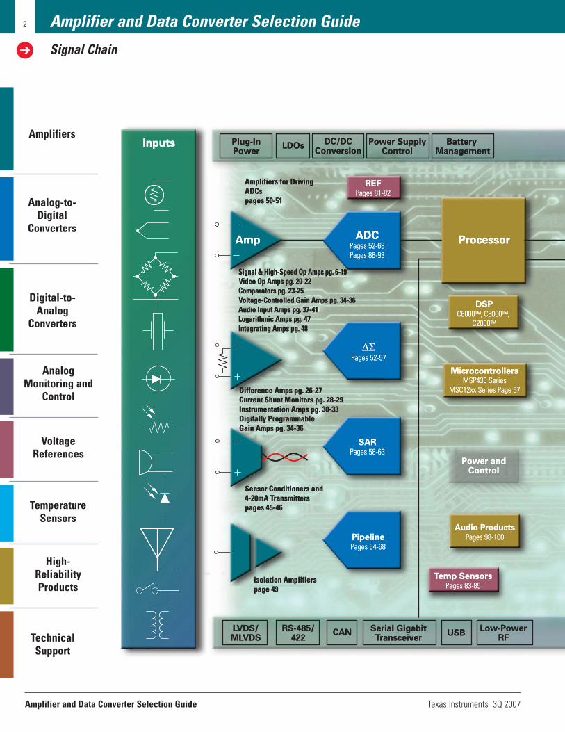
Signal Chain
Plug-InPower
Power SupplyControl
Battery Management
LDOsDC/DC
Conversion
LVDS/MLVDS
Serial GigabitTransceiver
USBRS-485/
422Low-Power
RFCAN
Temp SensorsPages 83-85
Inputs
Amp ADCPages 52-68Pages 86-93
Processor
REFPages 81-82
DSPC6000™, C5000™,
C2000™
MicrocontrollersMSP430 Series
MSC12xx Series Page 57
Power andControl
SARPages 58-63
PipelinePages 64-68
Signal & High-Speed Op Amps pg. 6-19 Video Op Amps pg. 20-22Comparators pg. 23-25Voltage-Controlled Gain Amps pg. 34-36 Audio Input Amps pg. 37-41Logarithmic Amps pg. 47Integrating Amps pg. 48
Difference Amps pg. 26-27Current Shunt Monitors pg. 28-29Instrumentation Amps pg. 30-33Digitally Programmable Gain Amps pg. 34-36
Sensor Conditioners and4-20mA Transmitters pages 45-46
Amplifiers for DrivingADCs pages 50-51
Isolation Amplifiers page 49
Audio ProductsPages 98-100
Pages 52-57
AnalogMonitoring and
Control
Voltage References
TemperatureSensors
High-ReliabilityProducts
Amplifiers
Analog-to-Digital
Converters
Digital-to-Analog
Converters
TechnicalSupport
Texas Instruments 3Q 2007 Amplifier and Data Converter Selection Guide
Amplifier and Data Converter Selection Guide
Signal Chain
3
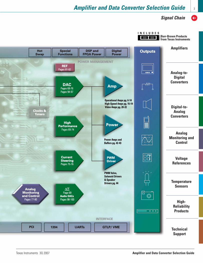
HotSwap
SpecialFunctions
DSP andFPGA Power
DigitalPower
DACPages 69-76Pages 94-97
High Performance
Pages 69-74
Amp
Power
PCI 1394 UARTs GTLP/ VME
INTERFACE
Current SteeringPages 75-76
Analog Monitoringand Control
Pages 77-80
PWM Driver
REFPages 81-82
Operational Amps pg. 6-14High-Speed Amps pg. 15-19Video Amps pg. 20-22
Power Amps andBuffers pg. 42-43
PWM Valve, Solenoid Drivers& SpeakerDrivers pg. 44
Clocks &Timers
POWER MANAGEMENT
Outputs
Page 69Audio DACs Pages 98-100
AnalogMonitoring and
Control
Voltage References
TemperatureSensors
High-ReliabilityProducts
Amplifiers
Analog-to-Digital
Converters
Digital-to-Analog
Converters
TechnicalSupport

Amplifier and Data Converter Selection Guide Texas Instruments 3Q 2007
Amplifier and Data Converter Selection Guide
Table of Contents
4
Precision Operational Amplifiers <50MHz
Overview/Technology Primer . . . . . . . . . . . . . . . . . . . . . . . . . . . . . . . . . . . . . . . . . . .7Low Offset Voltage . . . . . . . . . . . . . . . . . . . . . . . . . . . . . . . . . . . . . . . . . . . . . . . . . .8Low Power . . . . . . . . . . . . . . . . . . . . . . . . . . . . . . . . . . . . . . . . . . . . . . . . . . . . . . . . .9Low Noise . . . . . . . . . . . . . . . . . . . . . . . . . . . . . . . . . . . . . . . . . . . . . . . . . . . . . . . .10Low Input Bias Current . . . . . . . . . . . . . . . . . . . . . . . . . . . . . . . . . . . . . . . . . . . . . .11Wide Bandwidth . . . . . . . . . . . . . . . . . . . . . . . . . . . . . . . . . . . . . . . . . . . . . . . . . . .12Wide Supply Voltage . . . . . . . . . . . . . . . . . . . . . . . . . . . . . . . . . . . . . . . . . . . . . . . .13Single Supply Voltage . . . . . . . . . . . . . . . . . . . . . . . . . . . . . . . . . . . . . . . . . . . . . . .14
High-Speed Amplifiers >50MHz
Overview . . . . . . . . . . . . . . . . . . . . . . . . . . . . . . . . . . . . . . . . . . . . . . . . . . . . . . .15-19Video . . . . . . . . . . . . . . . . . . . . . . . . . . . . . . . . . . . . . . . . . . . . . . . . . . . . . . . . . .20-22
Comparators . . . . . . . . . . . . . . . . . . . . . . . . . . . . . . . . . . . . . . . . . . . . . . .23-25
Difference Amplifiers . . . . . . . . . . . . . . . . . . . . . . . . . . . . . . . . . . . . .26-27
Current Shunt Monitors
Overview . . . . . . . . . . . . . . . . . . . . . . . . . . . . . . . . . . . . . . . . . . . . . . . . . . . . . . . . .28Analog Output Current Shunt Monitors . . . . . . . . . . . . . . . . . . . . . . . . . . . . . . .28-29Digital Output Current Shunt Monitors . . . . . . . . . . . . . . . . . . . . . . . . . . . . . . .77-80
Instrumentation Amplifiers
Overview . . . . . . . . . . . . . . . . . . . . . . . . . . . . . . . . . . . . . . . . . . . . . . . . . . . . . . .30-31Single Supply . . . . . . . . . . . . . . . . . . . . . . . . . . . . . . . . . . . . . . . . . . . . . . . . . . . . . .32Dual Supply . . . . . . . . . . . . . . . . . . . . . . . . . . . . . . . . . . . . . . . . . . . . . . . . . . . . . . .33
Digitally Programmable Gain Amplifiers . . . . . . . . . . . . . . . . .34
Voltage-Controlled Gain Amplifiers . . . . . . . . . . . . . . . . . . . . .35-36
Audio Amplifiers . . . . . . . . . . . . . . . . . . . . . . . . . . . . . . . . . . . . . . . . . .37-41
Power Amplifiers and Buffers . . . . . . . . . . . . . . . . . . . . . . . . . . .42-43
Pulse Width Modulation Power Drivers . . . . . . . . . . . . . . . . . .44
Sensor Conditioners/4-20mA Transmitter . . . . . . . . . . . . .45-46
Logarithmic Amplifiers . . . . . . . . . . . . . . . . . . . . . . . . . . . . . . . . . . . . . .47
Integrating Amplifiers . . . . . . . . . . . . . . . . . . . . . . . . . . . . . . . . . . . . . . .48
Isolation Products . . . . . . . . . . . . . . . . . . . . . . . . . . . . . . . . . . . . . . . . . . . .49
Amplifiers for Driving ADCs . . . . . . . . . . . . . . . . . . . . . . . . . . . . . .50-51
Texas Instruments 3Q 2007 Amplifier and Data Converter Selection Guide
Amplifier and Data Converter Selection Guide
Table of Contents
5
Analog-to-Digital Converters (ADCs) by Architecture
Delta-Sigma (∆Σ) ADCs . . . . . . . . . . . . . . . . . . . . . . . . . . . . . . . . . . . . . . . . . . .52-55Wide Bandwidth ∆Σ ADCs . . . . . . . . . . . . . . . . . . . . . . . . . . . . . . . . . . . . . . . . . . .56Intelligent ADCs . . . . . . . . . . . . . . . . . . . . . . . . . . . . . . . . . . . . . . . . . . . . . . . . . . . .57SAR ADCs . . . . . . . . . . . . . . . . . . . . . . . . . . . . . . . . . . . . . . . . . . . . . . . . . . . . . .58-63Pipeline ADCs . . . . . . . . . . . . . . . . . . . . . . . . . . . . . . . . . . . . . . . . . . . . . . . . . . .64-68Analog Monitoring and Control (ADC and DAC) . . . . . . . . . . . . . . . . . . . . . . . .77-80
Digital-to-Analog Converters (DACs) by Architecture
Industrial Bipolar Delta-Sigma (∆Σ) DACs . . . . . . . . . . . . . . . . . . . . . . . . . . . . . . .69High-Accuracy, Industrial Bipolar and General-Purpose DACs . . . . . . . . . . . . .70-74Current Steering . . . . . . . . . . . . . . . . . . . . . . . . . . . . . . . . . . . . . . . . . . . . . . . . .75-76Audio . . . . . . . . . . . . . . . . . . . . . . . . . . . . . . . . . . . . . . . . . . . . . . . . . . . . . . . . . . .100
Analog Monitoring and Control
AMC Products . . . . . . . . . . . . . . . . . . . . . . . . . . . . . . . . . . . . . . . . . . . . . . . . . . .77-79Digital Current Shunt Monitors . . . . . . . . . . . . . . . . . . . . . . . . . . . . . . . . . . . . . . . .80
Voltage References . . . . . . . . . . . . . . . . . . . . . . . . . . . . . . . . . . . . . . . .81-82
Temperature Sensors . . . . . . . . . . . . . . . . . . . . . . . . . . . . . . . . . . . . .83-85
Quick Reference Selection Tables for Data Converters
Quick Reference ADC Selection Tables . . . . . . . . . . . . . . . . . . . . . . . . . . . . . . .86-93Quick Reference DAC Selection Tables . . . . . . . . . . . . . . . . . . . . . . . . . . . . . . .94-97Quick Reference Touch Screen Controllers with/without Audio Selection Tables . . . .98Quick Reference Audio Converters Selection Tables . . . . . . . . . . . . . . . . . . . .98-100
Design and Evaluation Tools
TINA-TI™/Spice Module . . . . . . . . . . . . . . . . . . . . . . . . . . . . . . . . . . . . . . . . . . . .101Amplifiers Design Center . . . . . . . . . . . . . . . . . . . . . . . . . . . . . . . . . . . . . . . . . . . .101FilterPro™, SARdriverPro™ and MDACBufferPro™ . . . . . . . . . . . . . . . . . . . . . . . .102Digitally Calibrated Sensor Signal Condition and 4-20mA Evaluation Modules . . . .103Signal Chain Prototyping System . . . . . . . . . . . . . . . . . . . . . . . . . . . . . . . . . .104-105Evaluation Boards and ADCPro™ Software . . . . . . . . . . . . . . . . . . . . . . . . . . . . .106Data Converter Plug-In (DCP) for Code Composer StudioTM IDE . . . . . . . . . .107-110Application Reports . . . . . . . . . . . . . . . . . . . . . . . . . . . . . . . . . . . . . . . . . . . .111-114Reference Designs . . . . . . . . . . . . . . . . . . . . . . . . . . . . . . . . . . . . . . . . . . . . . . . . .114Device Index . . . . . . . . . . . . . . . . . . . . . . . . . . . . . . . . . . . . . . . . . . . . . . . . . 115-118Worldwide Technical Support . . . . . . . . . . . . . . . . . . . . . . . . . . . . . . . . . . . . . . . .119

Amplifier and Data Converter Selection Guide Texas Instruments 3Q 2007
6 Amplifiers
Texas Instruments (TI) offers a wide range ofop amp types including high precision,microPower, low voltage, high voltage, highspeed and rail-to-rail in several differentprocess technologies. TI has developed theindustry's largest selection of low-power andlow-voltage op amps with features designedto satisfy a very wide range of applications.To help facilitate the selection process, aninteractive online op amp parametric searchengine is available at amplifier.ti.com/searchwith links to all op amp specifications.
Design Considerations
Choosing the best op amp for an applicationinvolves consideration of a variety of inter-related requirements. In doing so, designersmust often consider conflicting size, cost andperformance objectives. Even experiencedengineers can find the task daunting, but itneed not be so. Keeping in mind the followingissues, the choices can quickly be narrowedto a manageable few.
Supply voltage (VS)—tables include low voltage (< 2.7V min) and wide voltage range(> 5V min) sections. Other op amp selectioncriteria (e.g., precision) can be quickly exam-ined in the supply range column for anappropriate choice. Applications operatingfrom a single power supply may require rail-to-rail performance and consideration of precision-related parameters.
Precision—primarily associated with inputoffset voltage (VOS) and its change withrespect to temperature drift, PSRR andCMRR. It is generally used to describe opamps with low input offset voltage and lowinput offset voltage temperature drift.Precision op amps are required when amplifying tiny signals from thermocouplesand other low-level sensors. High-gain ormulti-stage circuits may require low offset voltage.
Gain bandwidth product (GBW)—the gainbandwidth of a voltage-feedback op ampdetermines its useful bandwidth in an application. The maximum available bandwidthis approximately equal to the gain bandwidthdivided by the closed-loop gain of the applica-tion. For voltage feedback amplifiers, GBW isa constant. Many applications benefit fromchoosing a much wider bandwidth/slew rate
op amp to achieve low distortion, excellentlinearity, good gain accuracy, gain flatness or other behavior that is influenced by feedback factors.
Power (IQ requirements)—a significant issuein many applications. Because op amps canhave a considerable impact on the overallsystem power budget, quiescent current,especially in battery-powered applications, is a key design consideration.
Rail-to-rail performance—rail-to-rail output provides maximum output voltageswing for widest dynamic range. This may beparticularly important with low operatingvoltage where signal swings are limited.Rail-to-rail input capability is often requiredto achieve maximum signal swing in buffer(G = 1) single-supply applications. It can beuseful in other applications, depending onamplifier gain and biasing considerations.
Voltage noise (VN)—amplifier-generatednoise may limit the ultimate dynamic range,accuracy or resolution of a system. Low-noise op amps can improve accuracy, even inslow DC measurements.
Input bias current (IB)—can create offseterror by reacting with source or feedbackimpedance. Applications with high sourceimpedance or high impedance feedback elements (such as transimpedance amplifiersor integrators) often require low input bias
current. FET-Input and CMOS op amps generally provide very low input bias current.
Slew rate—the maximum rate of change ofthe amplifier output. It is important whendriving large signals to high frequency. Theavailable large signal bandwidth of an opamp is determined by the slew rate SR/.707(2π)VP.
Package size—TI offers a wide variety ofmicroPackages, including WCSP, SOT23,SC70 and small, high power-dissipatingPowerPAD™ packages to meet space-sensitive and high-output drive requirements.Many TI single-channel op amps are available in SOT23, with some dual amplifiers in SOT23-8.
Shutdown mode—an enable/disable function that places the amp in a highimpedance state, reducing quiescent currentin many cases to less than 1µA. Allowsdesigners to use wide bandwidth op amps inlower power applications, enabling themonly when they are needed.
Decompensated amplifiers—for applications with gain greater than unitygain (G > 1), decompensated amps provide significantly higher bandwidth,improved slew rate and lower distortion overtheir unity-gain stable counterparts on thesame quiescent current or noise.
What is the amplitude of the input signal?To ensure signal errors are small relative tothe input signal, small input signals requirehigh precision (e.g., low offset voltage)amplifiers. Ensure that the amplified outputsignal stays within the amplifier output voltage.
Will the ambient temperature vary?Op amps are sensitive to temperaturevariations, so it is important to consideroffset voltage drift over temperature.
Does the common-mode voltage vary? Make sure the op amp is operated within its common-mode range and has anadequate common-mode rejection ratio
(CMRR). Common-mode voltage will induceadditional offset voltage.
Does the power supply voltage vary?Power supply variations affect the offset voltage. This may be especiallyimportant in battery-powered applications.
Precision Application Examples• High gain circuits (G > 100)• Measuring small input signals
(e.g., from a thermocouple)• Wide operating temperature range
circuits (i.e., in automotive or industrial applications)
• Single-supply ≤ 5V data-acquisition systems where input voltage span is limited
Common Op Amp Design Questions
Texas Instruments 3Q 2007 Amplifier and Data Converter Selection Guide
Amplifiers 7
Technology Primer
Understanding the relative advantages ofbasic semiconductor technologies will help inselecting the proper device for a specificapplication.
CMOS Amps—when low voltage and/or lowpower consumption, excellent speed/power ratio,rail-to-rail performance, low cost and smallpackaging are primary design considerations,choose microPackaged CMOS amps boastingthe highest precision in the industry.
High-Speed Bipolar Amps—when the highestspeed at the lowest power is required, bipolartechnology delivers the best performance.Extremely good power gain gives very highoutput power and full power bandwidths onthe lowest quiescent power. Higher voltage requirements are also only satisfied in bipolartechnologies.
Precision Bipolar Amps—excel in limitingerrors relating to offset voltage. These ampsinclude low offset voltage and temperaturedrift, high open-loop gain and common-moderejection. Precision bipolar op amps are usedextensively in applications where the source
impedance is low, such as a thermocoupleamplifier, and where voltage errors, offsetvoltage and drift, are crucial to accuracy.
Low IB FET Amps—when input impedance isvery high, FET-input amps provide better over-all precision than bipolar-input amps becauseof very low input bias current. Using a bipolaramp in applications with high source imped-ance (e.g., 500MΩ pH probe), the offset, driftand noise produced by bias currents flowingthrough the source would render the circuitvirtually useless. When low current errors arerequired, FET amps provide extremely lowinput bias current, low offset current andhigh input impedance.
Dielectrically Isolated FET (Difet™) Amps—Difet processing enables the design ofextremely low input leakage amplifiers byeliminating the substrate junction diode present in junction isolated processes. Thistechnique yields very high-precision, low-noise op amps. Difet processes also minimizeparasitic capacitance and output transistor saturation effects, resulting in improvedbandwidth and wider output swing.
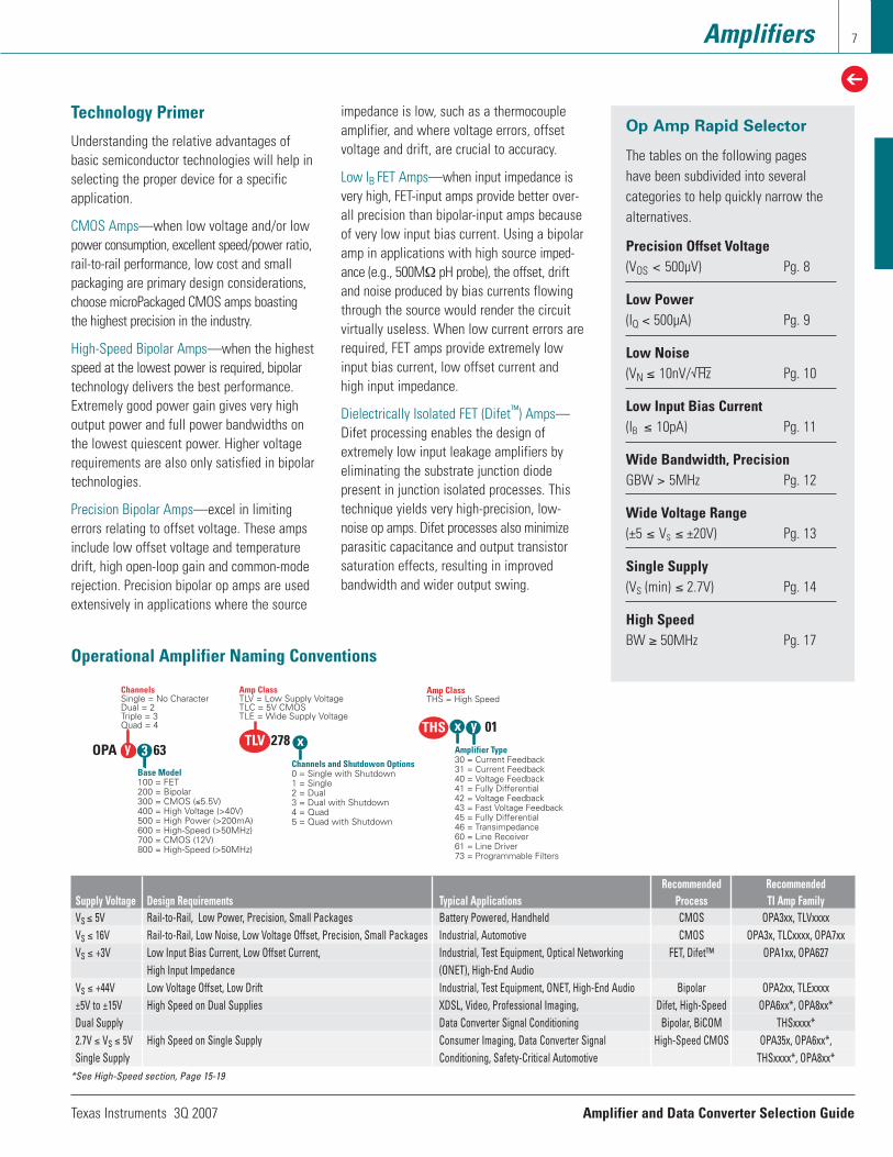
ChannelsSingle = No CharacterDual = 2Triple = 3Quad = 4
OPA y 3 63Base Model100 = FET200 = Bipolar300 = CMOS (≤5.5V)400 = High Voltage (>40V)500 = High Power (>200mA)600 = High-Speed (>50MHz)700 = CMOS (12V)800 = High-Speed (>50MHz)
Channels and Shutdowon Options0 = Single with Shutdown1 = Single2 = Dual3 = Dual with Shutdown4 = Quad5 = Quad with Shutdown
Amp ClassTLV = Low Supply VoltageTLC = 5V CMOSTLE = Wide Supply Voltage
TLV 278 x
Amp ClassTHS = High Speed
THS x y 01Amplifier Type30 = Current Feedback31 = Current Feedback40 = Voltage Feedback41 = Fully Differential42 = Voltage Feedback43 = Fast Voltage Feedback45 = Fully Differential46 = Transimpedance60 = Line Receiver61 = Line Driver73 = Programmable Filters
Op Amp Rapid Selector
The tables on the following pages have been subdivided into several categories to help quickly narrow thealternatives.
Precision Offset Voltage(VOS < 500µV) Pg. 8
Low Power(IQ < 500µA) Pg. 9
Low Noise(VN ≤ 10nV/ Hz Pg. 10
Low Input Bias Current(IB ≤ 10pA) Pg. 11
Wide Bandwidth, PrecisionGBW > 5MHz Pg. 12
Wide Voltage Range(±5 ≤ VS ≤ ±20V) Pg. 13
Single Supply(VS (min) ≤ 2.7V) Pg. 14
High SpeedBW ≥ 50MHz Pg. 17
Recommended Recommended Supply Voltage Design Requirements Typical Applications Process TI Amp FamilyVS ≤ 5V Rail-to-Rail, Low Power, Precision, Small Packages Battery Powered, Handheld CMOS OPA3xx, TLVxxxxVS ≤ 16V Rail-to-Rail, Low Noise, Low Voltage Offset, Precision, Small Packages Industrial, Automotive CMOS OPA3x, TLCxxxx, OPA7xxVS ≤ +3V Low Input Bias Current, Low Offset Current, Industrial, Test Equipment, Optical Networking FET, Difet™ OPA1xx, OPA627
High Input Impedance (ONET), High-End AudioVS ≤ +44V Low Voltage Offset, Low Drift Industrial, Test Equipment, ONET, High-End Audio Bipolar OPA2xx, TLExxxx±5V to ±15V High Speed on Dual Supplies XDSL, Video, Professional Imaging, Difet, High-Speed OPA6xx*, OPA8xx*Dual Supply Data Converter Signal Conditioning Bipolar, BiCOM THSxxxx*2.7V ≤ VS ≤ 5V High Speed on Single Supply Consumer Imaging, Data Converter Signal High-Speed CMOS OPA35x, OPA6xx*, Single Supply Conditioning, Safety-Critical Automotive THSxxxx*, OPA8xx*
*See High-Speed section, Page 15-19
Operational Amplifier Naming Conventions
Amplifier and Data Converter Selection Guide Texas Instruments 3Q 2007
Amplifiers
Precision Operational Amplifiers
8
1.8V, Zero-Offset, Zero-Drift, Ultra-Low-Power, RRIO, CMOS AmplifiersOPA333, OPA2333
Get samples, datasheets, and app reports at: www.ti.com/OPA333 and www.ti.com/sc/device/OPA2333
Key Features• Low offset voltage: 10µV (max)• Zero drift: 0.05µV/°C (max)• 0.01Hz to 10Hz noise: 1.1µVPP• Quiescent current: 17µA• Single-supply operation: 1.8V to 5.5V• Rail-to-rail input/output• microSize packages: SC70 and SOT23
Applications• Temperature measurement• Electronic scales• Medical instrumentation• Battery-powered instruments• Handheld test equipment
The OPA333 series of CMOS operational amplifiers are optimized for low-voltage, single-supplyoperation and combine TI’s proprietary zero-drift techniques to provide very low offset voltage(10µV max) and near-zero drift over time and temperature. These miniature, high-precision, lowquiescent current amplifiers offer high-impedance inputs that have a commonmode range100mV beyond the rails and rail-to-rail output that swings within 50mV of the rails.
Low Offset Voltage Operational Amplifiers (VOS < 500µV)IQ Per Slew VOS VOS VN at
VS VS Ch. GBW Rate (25°C) Drift IB CMRR 1kHz Rail-(V) (V) (mA) (MHz) (V/µs) (mV) (µV/°C) (pA) (dB) (nV// Hz) Single to-
Device Description/Technology Ch. (min) (max) (max) (typ) (typ) (max) (typ) (max) (min) (typ) Supply Rail Package(s) Price*
OPAy334/5 Zero-Drift, SHDN, CMOS 1, 2 2.7 5.5 0.35 2 1.6 0.005 0.02 200 110 — Y Out SOT-23, MSOP, SOIC $1.00 OPAy734/5 12V, Auto-Zero, SHDN, CMOS 1, 2 2.7 12 0.75 1.6 1.5 0.005 0.01 200 115 110 Y Out SOT-23, SOIC $1.25 OPAy333 µPower, Zero Drift, CMOS 1, 2 1.8 5.5 0.025 0.35 0.16 0.01 0.02 200 106 — Y I/O SC-70, SOT-23, SOIC $0.95 OPAy277 Precision, Bipolar 1, 2, 4 4 36 0.825 1 0.8 0.02 0.1 1000 130 8 N N SON, SOIC, PDIP $0.85 OPA378 Low Power, Wideband 1,2 1.8 5.5 0.100 1 0.5 0.025 0.1 1000 100 15 Y I/O SC70, SOT-23, SOIC $0.95OPAy380 Auto-Zero, 85MHz, TIA, CMOS 1, 2 2.7 5.5 8.8 90 80 0.025 0.03 50 100 110 Y Out MSOP, SOIC, SSOP $1.95 OPAy381 Precision, 18MHz, TIA, CMOS 1, 2 2.7 5.5 1 18 12 0.025 0.03 50 100 110 Y Out MSOP, SON $1.45 TLC2652A Low Offset, Chopper Stabilized 1 3.8 16 2.4 1.9 3.1 0.001 0.003 100 120 23 N N SOIC $2.20OPAy211 Low Offset Drift, Bipolar 1, 2 4.5 36 3.6 58 27 0.25 0.2 15,000 114 1.1 N Out SOIC, MSOP, SON $3.45OPAy227/28 Low Noise, Bipolar 1, 2, 4 5 36 3.8 8 2.3 0.075 0.1 10000 120 3 N N SOIC, PDIP $1.10 OPA827 Precision, FET Input 1, 2 8 36 4.5 18 22 0.25 1 3 108 4.5 N N SOIC, MSOP $5.75 TLE2027/37 Wide Supply, Low Noise, Bipolar 1 8 38 5.3 13, 50 2.8, 7.5 0.1 0.4 90000 100 2.5 N N SOIC, PDIP $0.90 OPAy234 Low Power, Wide Supply, Bipolar 1, 2, 4 2.7 36 0.3 0.35 0.2 0.1 0.5 25000 96 25 N N MSOP, SOIC $1.05 OPA627/37 Ultra-Low THD+N, Difet 1 9 36 7.5 16 55 0.1 0.4 1 106 5.2 N N PDIP, SOIC $12.25 OPAy336 µPower, CMOS 1, 2, 4 2.3 5.5 0.032 0.1 0.03 0.125 1.5 10 80 40 Y Out SOT-23, SOIC $0.40 OPAy727/8 e-trim™, Precision CMOS 1, 2 4 12 4.3 20 30 0.15 0.3 100 86 23 N N MSOP, SON $0.95 OPA365 Wideband, Zero-Crossover 1,2 2.2 5.5 5 50 25 0.2 1 10 100 5 Y I/O SOT-23-5,8SOIC $0.95OPAy241 µPower, Bipolar 1, 2, 4 2.7 36 0.03 0.035 0.01 0.25 0.4 20000 80 45 Y Out SOIC, DIP $1.15 OPAy251 µPower, ±15V Bipolar 1, 2, 4 2.7 36 0.038 0.035 0.01 0.25 0.5 20000 100 45 Y Out SOIC, DIP $1.15 OPA124 Wide Bandwidth, Bipolar 1 10 36 3.5 1.5 1.6 0.25 1 1 100 8 N N SOIC $3.95 TLC1078 Precision, CMOS 2 1.4 16 0.017 0.085 0.032 0.45 1.1 600 70 68 N N SOIC, DIP $2.30 TLV2211 Low Power, 10V, CMOS 1 2.7 10 0.025 0.065 0.025 0.45 0.5 150 70 22 Y Out SOT23 $0.42
•Suggested resale price in U.S. dollars in quantities of 1,000. New products are listed in bold red. Preview products are listed in bold blue.
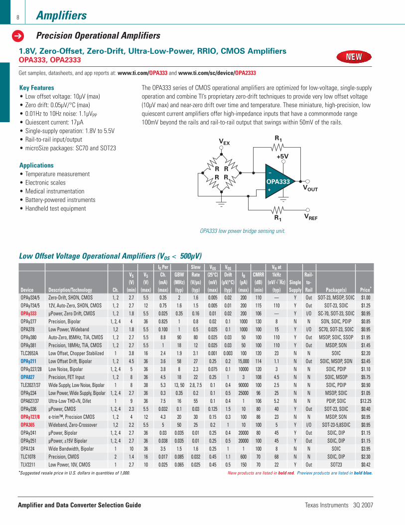
OPA333
R R
R R
VEXR1
R1
+5V
VOUT
VREF
–
+
OPA333 low power bridge sensing unit.
Texas Instruments 3Q 2007 Amplifier and Data Converter Selection Guide
Amplifiers
Precision Operational Amplifiers
9
Low-Power Operational Amplifiers (IQ < 500µA) Selection GuideIQ Per Slew VOS Offset VN at
VS VS Ch. GBW Rate (mV) Drift IB CMRR 1kHz Rail-(V) (V) (mA) (MHz) (V/µs) (25°C) (µV/°C) (pA) (dB) (nV/ Hz) to-
Device Description Ch. (min) (max) (max) (typ) (typ) (max) (typ) (max) (min) (typ) Rail Package(s) Price*
TLV240x 2.5V, Sub-µPower, SS, CMOS 1, 2, 4 2.5 16 0.00095 0.0055 0.0025 1.2 3 300 63 — I/O MSOP, PDIP, SOIC, SOT23, TSSOP $0.65 TLV224x Low Voltage, 1µA, SS, CMOS 1, 2, 4 2.5 12 0.0012 0.0055 0.002 3 3 500 55 — I/O MSOP, PDIP, SOIC, SOT23, TSSOP $0.60 OPA369 Lowest Power, Zero Crossover 1,2 1.8 5.5 0.001 0.01 0.005 1 2 10 100 160 I/O SC70, SOT23 $0.95OPAy349 1µA, SS, CMOS 1, 2 1.8 5.5 0.002 0.07 0.02 10 10 15 52 — I/O SC70, SOIC, SOT23 $0.75 OPAy333 µPower, SS, RRIO, Zero-Drift, CMOS 1,2 1.8 5.5 0.025 0.35 0.16 0.01 0.05 200 106 60 I/O SC70, SOT23, SOIC $0.95 OPA379 1.8V, Ultra-Low Power, CMOS 1, 2, 4 1.8 5.5 0.005 0.1 0.03 1.5 2.7 50 90 80 I/O SC70, SOT23, SOIC $0.75 TLC1078 Low Voltage, Precision, Bipolar 2 1.4 16 0.017 0.085 0.032 0.45 1.1 600 70 68 Out SOIC, PDIP $2.30 OPAy241 Bipolar, µPower, High CMRR, 1, 2, 4 2.7 36 0.035 0.35 0.1 0.25 0.4 20000 80 45 Out PDIP, SOIC $1.15 OPA703/4 12V, RRIO, General Purpose 1, 2, 4 4 12 0.2 1 0.6 0.75 4 10 70 45 I/O MSOP, SOIC, TSSOP, PDIP $0.40OPAy336 µPower, SS, CMOS 1, 2, 4 2.3 5.5 0.032 0.1 0.03 0.125 1.5 10 80 40 Out SOT23, SOIC $0.40 OPAy347 µPower, Low Cost, SS, CMOS 1, 2, 4 2.3 5.5 0.034 0.35 0.17 6 2 10 70 60 I/O SC70, SOT23, SOIC, PDIP $0.48 TLV245x µPower, SS, CMOS 1, 2, 4 2.7 6 0.035 0.22 0.12 1.5 0.3 5000 64 51 I/O SOT23, SOIC, PDIP $0.60 OPAy251 µPower, Precision, Bipolar 1, 2, 4 2.7 36 0.038 0.035 0.01 0.25 0.5 20000 100 45 Out SOIC, PDIP $1.15 OPA378 Wide Bandwidth, microPower, e-trim™ 1, 2 1.8 5.5 0.10 1 0.5 0.025 0.1 1000 100 15 I/O SC70, SOT23, SOIC $0.85OPAy244 µPower, SS, Low Cost, Bipolar 1, 2, 4 2.7 36 0.05 0.24 0.1 1.5 4 25000 84 22 N MSOP, PDIP, SOIC, SOT23, TSSOP $0.55 OPAy348 High Open-Loop Gain, SS, CMOS 1, 2, 4 2.1 5.5 0.065 1 0.5 5 2 10 70 35 I/O SC70, SOIC, SOT23, CSP $0.45 OPA345 Wideband, Single-Supply 1,2,4 2.7 5.5 0.25 4 4 0.5 2.5 10 80 32 I/O SOT23, SOIC, MSOP $1.20 OPA137 Low Cost, FET-Input 1,2,4 4.5 36 0.27 1 3.5 3 15 100 76 45 N SOT23, SOIC, DIP $0.60 OPA234 Low Power, Precision 1, 2, 4 2.7 36 0.3 0.35 0.2 0.1 0.5 25000 96 24 N MSOP, SOIC $1.05 OPAy334/5 Zero-Drift, Precision, CMOS, SS, SHDN 1, 2 2.7 5.5 0.35 2 0.5 0.005 0.02 200 110 — Out MSOP, SOIC, SOT23 $1.00
•Suggested resale price in U.S. dollars in quantities of 1,000. New products are listed in bold red. Preview products are listed in bold blue.
Ultra-Low-Power, 1µA, RRIO, Zero-Crossover Operational AmplifierOPA369
Get samples, datasheets, and app reports at: www.ti.com/sc/device/OPA369
Key Features• Ultra-low supply current: 1µA (max)• RRIO Zero-Crossover input topology • Excellent CMRR: 100dB • Low offset voltage: 1mV (max)• Excellent GBW for low power: 10kHz• microPackages: SC70-3, SOT23-3, MSOP
Applications• Battery-powered instruments• Portable devices• High impedance applications• Medical instruments• Precision integrators• Test equipment
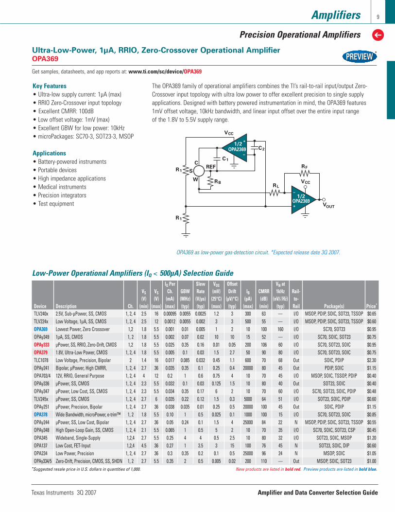
The OPA369 family of operational amplifiers combines the TI’s rail-to-rail input/output Zero-Crossover input topology with ultra low power to offer excellent precision to single supplyapplications. Designed with battery powered instrumentation in mind, the OPA369 features1mV offset voltage, 10kHz bandwidth, and linear input offset over the entire input range of the 1.8V to 5.5V supply range.
1/2
RF
VCCRL
VOUT
R1
R1
C1
REFC
W
S
RB
VCC
C2
OPA2369+
–
–
+1/2
OPA2369
OPA369 as low-power gas-detection circuit. *Expected release date 3Q 2007.

10 Amplifiers
Precision Operational Amplifiers
Low-Noise Operational Amplifiers (VN ≤ 10nV/ Hz)IQ Per Slew VOS VOS VN at
VS VS Ch. GBW Rate (25°C) Drift IB CMRR 1kHz Rail-(V) (V) (mA) (MHz) (V/µs) (mV) (µV/°C) (pA) (dB) (nV// Hz) Single to-
Device Description/Technology Ch. (min) (max) (max) (typ) (typ) (max) (typ) (max) (min) (typ) Supply Rail Package(s) Price*
OPAy211 Ultra-Low Noise, 1, 2 8 36 3.6 80 27 0.1 0.2 15000 114 1.1 N N MSOP, SOIC, SON $3.95 High Precision
TLE2027 Wide Supply, Bipolar 1 8 38 5.3 13 2.8 0.1 0.4 90000 100 2.5 N N SOIC $0.90 OPA300 Very Wide Bandwidth 1 2.7 5.5 12 150 80 2.5 5 5 66 3 Y Out SOT23-6,SOIC-8 $1.25OPA227 High Precision, Bipolar 1, 2, 4 5 36 3.8 8 2.3 0.075 0.1 10000 120 3 N N SOIC, PDIP $1.10 OPA228 High Speed, Precision, 1, 2, 4 5 36 3.8 33 10 0.075 0.1 10000 120 3 N N SOIC, PDIP $1.10 OPAy827 Ultra-Low THD+N, 1, 2 8 36 4.5 18 22 0.25 1 3 108 4.5 N N MSOP, SOIC $5.75
High-Precision OPAy350 Excellent ADC Driver, 1, 2, 4 2.7 5.5 7.5 38 22 0.5 4 10 76 5 Y I/O MSOP $0.85 OPA365 High Speed, Zero Crossover 1, 2 2.2 5.5 5 50 25 0.5 1 10 100 5 Y I/O SOT-23, SO-8 $0.95 OPA353 Good ADC Driver, 1, 2, 4 2.7 5.5 8 44 22 8 5 10 76 5 Y I/O SOT-23, SOIC $1.00
Low THD+N, CMOS OPA376 Low Offset, 5MHz 1, 2, 4 2.2 5.5 0.95 5 4 0.05 2 10 80 7.5 Y I/O SC70, SOT23, MSOP, $0.95
General Purpose SO8, TSSOPOPA627/37 Precision, High Speed, 1 9 36 7.5 16, 80 55, 135 0.1 0.4 1 106 5.2 N N SOIC $12.25
Difet™OPA376 Low Power RRIO 1, 2, 4 2.2 55 0.95 5 4 0.05 2 10 80 7.5 Y I/O SC70, SOT23 $0.95OPA121 Precision, Difet S 10 36 4.5 2 2 3 2 5 86 8 N N SOIC-8 $5.10OPAy277 High Precision 1, 2, 4 4 36 0.825 1 0.8 0.02 0.1 1000 130 8 N N SOIC, PDIP $0.85 OPA124 Low Noise, Precision, 1 10 36 7.5 1.5 1.6 0.25 2 1 100 8 N N PDIP $3.95
Bipolar TLC220x Precision, Low Power, 1, 2 4.6 16 1.5 1.8 2.5 0.5 0.5 100 85 8 Y Out SOIC, PDIP $1.65
LinCMOSOPAy132 Wide Bandwidth, FET-Input 1, 2, 4 4.5 36 4.8 8 20 0.5 2 50 96 8 N N SOIC $1.45 *Suggested resale price in U.S. dollars in quantities of 1,000. New products are listed in bold red. Preview products are listed in bold blue.
OPA211
3.6mA IQ
+15V
100µV
200mV
-15V
+
_
10
1 10 100 1kFrequency (Hz)
Vo
lta
ge
No
ise
(n
V/√
Hz
1.1nV/ Hz√
1.1nV/ Hz Noise, Low-Power, Precision Bipolar Operational Amplifier
OPA211, OPA2211
Get samples, datasheets, and app reports at: www.ti.com/OPA211 and www.ti.com/sc/device/OPA2211
OPA211 noise density vs. frequency. *Expected Release Date 4Q 2007.
Key Features• Low noise voltage: 1.1nV/ Hz at 1kHz • 100nVPP input voltage noise: 0.1Hz to10Hz • Low offset voltage: 100µV (max) • Low offset voltage drift: 0.2µV/°C (typ) • Unity gain bandwidth 58MHz • Wide supply range: ±2.25V to ±18V,
+4.5V to +36V • Rail-to-rail output • Output current: 30mA • Shutdown: 20µA (max)
Applications• Low-noise signal processing • High-performance ADC drivers• Active filters • Ultrasound amplifiers • Professional audio preamplifiers • Hydrophone amplifiers • MRI and CAT Scan
The OPA211 and OPA2211 use proprietary design techniques combined with a high voltage isolated silicon germanium process to deliver outstanding noise performance, (1.1nV/ Hz) precision (100µV) offset voltage and wide supply range from 4.5V to 36V single supply operationor ±2.25V to ±18V. Devices have a specified temperature range of –40°C to +125°C and operating temperature range of –55°C to +150°C. This performance is available in very smallpackaging 3mm x 3mm 8-pin DFN and the 8-pin MSOP.
Amplifier and Data Converter Selection Guide Texas Instruments 3Q 2007

Amplifiers
Precision Operational Amplifiers
11
JFET Input, High Precision, Low-Noise Operational AmplifierOPA827
Get samples, datasheets, and app reports at: www.ti.com/sc/device/OPA827
Key Features• Ultra-low-input bias current: 3pA • Low Offset: 250µV (max) • Drift: 1µV/°C • Low noise: 4.5nV/ Hz at 1kHz • Bandwidth: 18MHz • Packages:
•• Single: MSOP-8, SO-8 •• Dual: TSSOP-8, SO-8
Applications• Precision ±10V input front-ends • Transimpedance amplifiers • Active filters • ADC drivers • DAC output buffer • High-performance audio
The OPA827 and OPA2827 use proprietary design techniques combined with a high voltage isolated silicon germanium process and FET-input transistors to deliver high input impedance (1 x 10¹³Ω), outstanding noise performance, (4.5nV/ Hz) and high precision (250µV) offset voltage. Devices have specified temperature range of –40°C to +125°C. This performance is available in very small, 8-pin MSOP packaging.
OPA827
+15V
250µV
–15V
3.6mA IQ
+5V
ADS8505
±10V
Input
400nVPP0.1Hz to 10Hz Noise
1600nVPPClosest Competition
200n
V /
Div
PP
1s/Div Frequency (Hz)
OPA827 features extremely low noise for data acquisition.*Expected Release Date 4Q 2007.
Low Input Bias Current Operational Amplifiers (IB ≤≤ 10pA)IQ Per Slew VOS VOS VN at
VS VS Ch. GBW Rate (25°C) Drift IB CMRR 1kHz Rail-(V) (V) (mA) (MHz) (V/µs) (mV) (µV/°C) (pA) (dB) (nV// Hz) Single to-
Device Description/Technology Ch. (min) (max) (max) (typ) (typ) (max) (typ) (max) (min) (typ) Supply Rail Package(s) Price*
OPA129 Ultra-Low Bias, Difet™ 1 10 36 1.8 1 2.5 2 3 0.1 80 17 N N SOIC $3.20OPA124 Low Noise, High Precision 1 10 36 7.5 1.5 1.6 0.25 2 1 100 8 N N PDIP $3.95 OPA627/37 Ultra-Low THD+N, Difet 1 9 36 7.5 16, 80 55, 135 0.1 0.4 1 106 5.2 N N PDIP, SOIC $12.25 OPAy827 Low Noise, Precision, FET-Input 1, 2 8 36 4.5 18 22 0.25 1 3 108 4.5 N N MSOP, SOIC $5.75 OPA344 Low Power, RRIO, SS 1, 2, 4 2.7 5.5 0.25 1 1 0.5 2.5 10 80 32 Y I/O MSOP, DIP, SOIC $0.55 OPA363 1.8V, RRIO, High CMRR 1, 2 2.7 5.5 0.75 7 5 0.5 3 10 74 17 Y I/O MSOP, SOIC, SOT23 $0.60 OPAy336 SS, µPower, CMOS 1, 2, 4 2.3 5.5 0.032 0.1 0.03 0.125 1.5 10 80 40 Y Out SOT23, SOIC $0.40 OPAy340 CMOS, Wide Bandwidth 1, 2, 4 2.7 5.5 0.95 5.5 6 0.5 2.5 10 80 25 Y I/O MSOP, SOIC, SOT23, TSSOP $0.80 OPAy350 Excellent ADC Driver, Low Noise 1, 2, 4 2.7 5.5 7.5 38 22 0.5 4 10 76 5 Y I/O PDIP, MSOP, SOIC $0.85 OPAy365 High Speed, Zero-Crossover, 1, 2 2.2 5.5 5 50 25 0.5 1 10 100 5 Y IN SOT23, SO8 $0.95
CMOS OPA376 Low Offset, 5MHz 1, 2, 4 2.2 5.5 0.95 5 4 0.05 2 10 80 7.5 Y I/O SC70, SOT23, MSOP, $0.95
SO8, TSSOP*Suggested resale price in U.S. dollars in quantities of 1,000. New products are listed in bold red. Preview products are listed in bold blue.
Texas Instruments 3Q 2007 Amplifier and Data Converter Selection Guide
Amplifiers
Precision Operational Amplifiers
12
2.2V, 50MHz, 5nV/ Hz, Zero-Crossover Operational Amplifier
OPA365
Get datasheets at: www.ti.com/OPA365
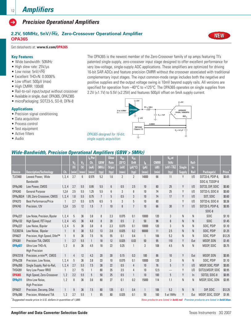
OPA365 designed for 16-bit, single supply acquisition.
Key Features• Wide bandwidth: 50MHz• High slew rate: 25V/µs• Low noise: 5nV/ Hz• Excellent THD+N: 0.0006%• Low offset: 500µV (max)• High CMRR: 100dB• Rail-to-rail input/output without crossover• Available in single, dual: OPA365, OPA2365 • microPackaging: SOT23-5, SO-8, DFN-8
Applications• Precision signal conditioning• Data acquisition• Process control• Test equipment• Active filters• Audio
The OPA365 is the newest member of the Zero-Crossover family of op amps featuring TI’spatented single-supply, zero-crossover input stage designed to offer excellent performance forvery low-voltage, single-supply ADC applications. These amplifiers are optimized for driving 16-bit SAR ADCs and feature precision CMRR without the crossover associated with traditionalcomplementary input stages. The input common-mode range includes both the negative andpositive supplies and the output voltage swing is 10mV beyond supply rails. All versions arespecified for operation from –40°C to +125°C. The OPA365 operates on single supplies from2.2V (±1.1V) to 5.5V (±2.25V) and features 500µV offset on 5mA supply current.
Wide-Bandwidth, Precision Operational Amplifiers (GBW > 5MHz)IQ Per Slew VOS VOS VN at
VS VS Ch. GBW Rate (25°C) Drift IB CMRR 1kHz Rail-(V) (V) (mA) (MHz) (V/µs) (mV) (µV/°C) (pA) (dB) (nV// Hz) Single to-
Device Description/Technology Ch. (min) (max) (max) (typ) (typ) (max) (typ) (max) (min) (typ) Supply Rail Package(s) Price*
TLV2460 Lowest Power, Wide 1, 2, 4 2.7 6 0.575 5.2 1.6 2 2 14000 66 11 Y I/O SOT23-6, PDIP-8, $0.65Bandwidth SOIC-8, TSSOP-8
OPAy340 Low Power, CMOS 1, 2, 4 2.7 5.5 0.95 5.5 6 0.5 2.5 10 80 25 Y I/O SOT23, DIP, SOIC $0.80 OPA343 General Purpose 1,2,4 2.5 5.5 1.25 5.5 6 3 8 10 74 25 Y I/O SOT23-5, SOIC-8 $0.60OPAy363/4 1.8V, Zero-Crossover, CMOS 1, 2, 4 1.8 5.5 0.75 7 5 0.5 3 10 74 17 Y I/O SOT, SOIC $0.60 OPA373 Best Performance/Price 1 2.7 5.5 0.75 6.5 5 3 5 10 80 Y I/O SOT23-6, SOIC-8 $0.36OPA743 Precision, 12V 1,2,4 3.5 12 1.5 7 10 8 7 10 66 30 Y I/O SOT23-5, PDIP-8, $0.95
SOIC-8OPAy227 Low Noise, Precision, Bipolar 1, 2, 4 5 36 3.8 8 2.3 0.075 0.1 10000 120 3 N N SOIC $1.10 OPAy132 High Speed, FET-Input 1, 2, 4 4.5 36 4.8 8 20 0.5 2 50 96 8 N N SOIC $1.45 OPAy227 Low Noise, Bipolar 1, 2, 4 5 36 3.8 8 2.3 0.075 0.1 10000 120 3 N N SOIC, PDIP $1.10 TLE2027A Low Noise, Bipolar 1 8 38 5.3 13 2.8 0.025 0.2 90000 11 2.5 N N SOIC, PDIP $1.25 OPA627 Precision, High Speed, Difet™ 1 9 36 7.5 16 55 0.1 0.4 1 106 5.2 N N SOIC, PDIP $12.25 OPA381 Precision TIA, CMOS 1 2.7 5.5 1 18 12 0.025 0.03 50 95 110 Y Out MSOP, SON $1.45 OPAy827 Ultra-Low THD+N, 1, 2 8 36 4.5 18 22 0.25 1 3 108 4.5 N N MSOP, SOIC $5.75
High PrecisionOPA727/8 Precision, e-trim™, CMOS 1 4 12 4.3 20 30 0.15 0.3 100 86 10 Y Out MSOP, SON $0.95 OPAy228 Precision, Low Noise, 1, 2, 4 5 36 3.8 33 10 0.075 0.1 10000 120 3 N N SOIC, PDIP $1.10 OPAy350 Single Supply, Rail-to-Rail, 1, 2, 4 2.7 5.5 7.5 38 22 0.5 4 10 76 5 Y I/O MSOP, SOIC, PDIP $0.85 THS4281 Very Low Power RRIO 1 2.7 15 1 80 35 3.5 4 10 12.5 — Y I/O SOT23,MSOP, SOIC $0.95 OPA365 High Speed, Zero-Crossover 1, 2 2.2 5.5 5 50 25 0.5 1 10 100 5 Y In SOT23, SOIC-8 $0.95 OPAy211 Ultra-Low Noise, 1, 2 8 36 3.6 80 27 0.1 0.2 15000 114 1.1 N N MSOP, SOIC, SON $3.95
High Precision OPA637 Precision, Decomp, Difet 1 9 36 7.5 80 135 0.1 0.4 1 106 5.2 N N DIP, SOIC $12.25 OPAy380 Precision, Wideband TIA 1, 2 2.7 5.5 1 85 80 0.025 0.1 50 100 5 at 1MHz Y Out MSOP, SOIC, SSOP $1.95
*Suggested resale price in U.S. dollars in quantities of 1,000. New products are listed in bold red. Preview products are listed in bold blue.
Amplifier and Data Converter Selection Guide Texas Instruments 3Q 2007
Texas Instruments 3Q 2007 Amplifier and Data Converter Selection Guide
Amplifiers
Precision Operational Amplifiers
13
Wide Voltage Range Operational Amplifiers (±5V < VS < ±20V) Selection GuideIQ Per Slew VOS VOS VN at
VS VS Ch. GBW Rate (25°C) Drift IB CMRR 1kHz Rail-(V) (V) (mA) (MHz) (V/µs) (mV) (µV/°C) (pA) (dB) (nV/ Hz) Single to-
Device Description Ch. (min) (max) (max) (typ) (typ) (max) (typ) (max) (min) (typ) Supply Rail Package(s) Price*
TLE214x Widest Supply, Low Noise, High Speed 1, 2, 4 4 44 4.5 5.9 45 0.9 1.7 1500000 85 10.5 N N PDIP, SOIC $0.55TLE202x Low Power, FET-Input 1, 2, 4 4 40 0.3 1.2 0.5 0.6 2 70000 85 17 N N SOIC, TSSOP, PDIP $0.45 TLE2027 Excalibur™, Low Noise, Bipolar 1 8 38 5.3 13/50 2.8 0.1 0.4 90000 100 2.5 N N SOIC, PDIP $0.90 TLE2037 Excalibur, Low Noise, G≥5, Bipolar 1 8 38 5.3 13/50 2.8 0.1 0.4 90000 100 2.5 N N SOIC, PDIP $0.90 OPAy241 µPower, Precision, Bipolar 1, 2, 4 2.7 36 0.03 0.035 0.01 0.25 0.4 20000 100 45 Y Out SOIC, PDIP $1.15 OPAy251 µPower, Precision, Bipolar 1, 2, 4 2.7 36 0.038 0.035 0.01 0.25 0.5 20000 100 45 Y Out PDIP, SOIC $1.15 OPAy244 µPower, Low Cost, Bipolar 1, 2, 4 2.6 36 0.05 0.43 0.1 1.5 4 25000 84 22 N N SOT-23, SOIC, PDIP $0.55 OPAy137 Low Cost, FET-Input 1, 2, 4 4.5 36 0.27 1 3.5 3 15 100 76 45 N N SOT23, SOIC $0.60 OPAy234 Low Power, Precision, Bipolar 1, 2, 4 2.7 36 0.35 0.35 0.2 0.1 0.5 25000 91 25 N N MSOP, SOIC $1.05 OPAy237 Low Cost, Low Power, Bipolar 1, 2 2.7 36 0.35 1.4 0.5 0.75 2 40000 78 28 N N SOT23, SOIC $0.55 OPAy130 Low Power, FET-Input 1, 2, 4 4.5 36 0.65 1 2 1 2 20 90 16 N N SOIC $1.40 OPAy277 High Precision, Low Power, Bipolar 1, 2, 4 4 36 0.825 1 0.8 0.02 0.1 1000 130 8 N N SON, SOIC $0.85 OPAy131 General Purpose, FET-Input 1, 2, 4 9 36 1.75 4 10 0.75 2 50 80 15 N N SOIC $0.75 OPAy227 Precision, Low Noise, Bipolar 1, 2, 4 5 36 3.8 8 2.3 0.075 0.1 10000 120 3 N N PDIP, SOIC $1.10 OPAy228 Precision, Low Noise, G 5, Bipolar 1, 2, 4 5 36 3.8 33 11 0.075 0.1 10000 120 3 N N PDIP, SOIC $1.10 OPAy132 Wide Bandwidth, FET-Input 1, 2, 4 4.5 36 4.8 8 20 0.5 2 50 96 8 N N SOIC $1.45 OPA124 Low Noise, Precision, Bipolar 1 10 36 7.5 1.5 1.6 0.25 2 1 100 8 N N PDIP $3.95 OPA627 Ultra-Low THD+N, Difet™ 1 9 36 7.5 16 55 0.1 0.4 1 106 5.2 N N PDIP, SOIC $12.25 OPA637 Ultra-Low THD+N,G5, Difet 1 9 36 7.5 80 135 0.1 0.4 1 106 5.2 N N PDIP, SOIC $12.25 OPAy211 Ultra-Low Noise, High-Precision 1, 2 8 36 3.6 80 27 0.1 0.2 15000 114 1.1 N N MSOP, SOIC, SON $3.95 OPAy827 Ultra-Low THD+N, High-Precision 1, 2 8 36 4.5 18 22 0.25 1 3 108 4.5 N N MSOP, SOIC $5.75 TLV240x 2.5V, 1µA, Bipolar 1, 2, 4 2.5 16 0.00095 0.0055 0.0025 1.2 3 300 63 800 Y I/O SOT23, SOIC, PDIP $0.65 TLV238x Low Power, RRIO, Bipolar 1, 2 2.7 16 0.01 0.16 0.06 6.5 1.1 60 72 90 Y I/O SOT, SOIC, PDIP $0.60 TLC220x Precision, Low Noise, Bipolar 1, 2 4.6 16 1.5 1.8 2.5 0.5 0.5 100 85 8 Y Out SOIC, PDIP $1.65 TLC08x Low Noise, Wide Bandwidth, Bipolar 1, 2, 4 4.5 16 2.5 10 16 1 1.2 50 100 8.5 N N MSOP, SOIC, PDIP $0.45 TLV237x 550µA, 3MHz, SHDN 1, 2, 4 2.7 15 0.66 3 2.4 4.5 2 60 57 39 Y I/O SOT23, MSOP $0.43 OPAy703/4 12V, Low Power, SHDN, CMOS 1, 2, 4 4 12 0.2 1 0.6 0.75 4 10 70 45 Y I/O MSOP, SOIC, DIP $1.30 OPAy734/5 12V, Auto-Zero Precision, SHDN 1, 2 2.7 12 0.75 1.6 1.5 0.005 0.05 200 115 150 Y Out SOT23, SOIC $1.25 OPAy743 12V, 7MHz, CMOS 1, 2, 4 3.5 12 1.5 7 10 7 8 10 66 30 Y I/O MSOP, SOIC $0.95 OPAy727/8 20MHz, e-trim™ Precision CMOS 1, 2, 4 4 12 4.3 90 30 0.25 0.3 100 86 23 N N MSOP, SON $0.95 OPAy725/6 Very Low Noise, SHDN 1, 2 4 12 5.5 20 30 3 4 200 88 23 Y Out SOT23, SOIC $0.90
*Suggested resale price in U.S. dollars in quantities of 1,000. Preview products are listed in bold blue.
Amplifier and Data Converter Selection Guide Texas Instruments 3Q 2007
Amplifiers
Precision Operational Amplifiers
14
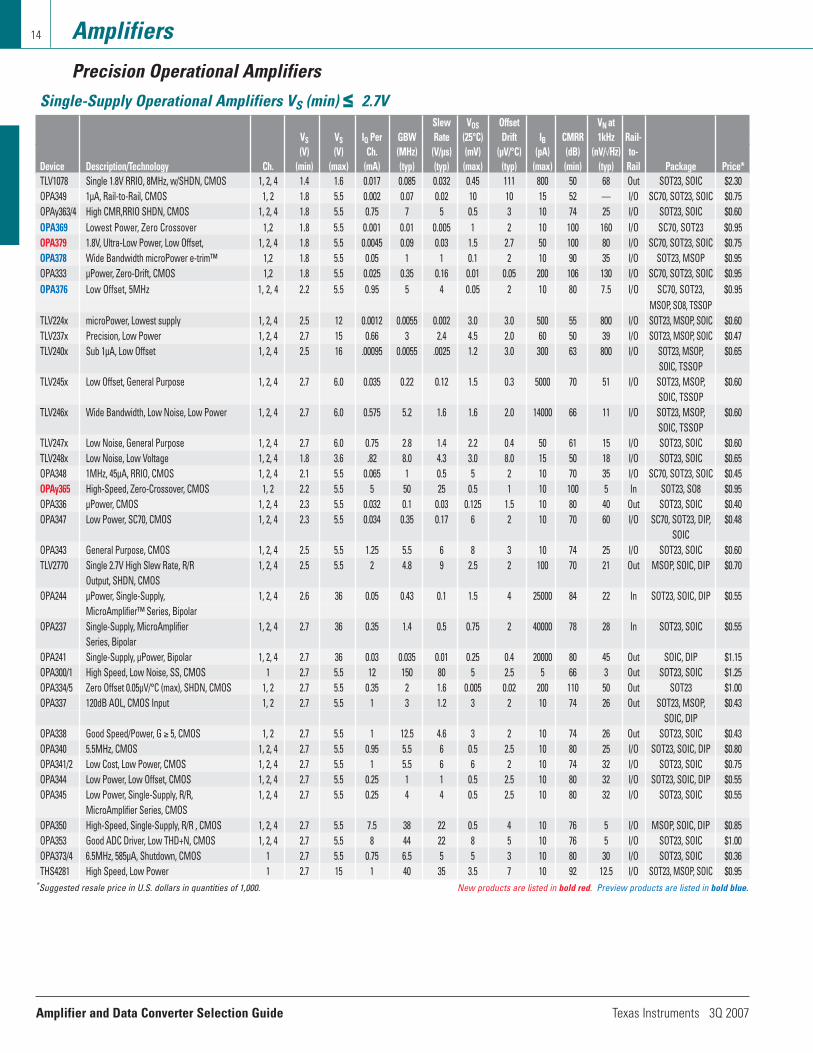
Single-Supply Operational Amplifiers VS (min) ≤≤ 2.7VSlew VOS Offset VN at
VS VS IQ Per GBW Rate (25°C) Drift IB CMRR 1kHz Rail-(V) (V) Ch. (MHz) (V/µs) (mV) (µV/°C) (pA) (dB) (nV/ Hz) to-
Device Description/Technology Ch. (min) (max) (mA) (typ) (typ) (max) (typ) (max) (min) (typ) Rail Package Price*TLV1078 Single 1.8V RRIO, 8MHz, w/SHDN, CMOS 1, 2, 4 1.4 1.6 0.017 0.085 0.032 0.45 111 800 50 68 Out SOT23, SOIC $2.30 OPA349 1µA, Rail-to-Rail, CMOS 1, 2 1.8 5.5 0.002 0.07 0.02 10 10 15 52 — I/O SC70, SOT23, SOIC $0.75 OPAy363/4 High CMR,RRIO SHDN, CMOS 1, 2, 4 1.8 5.5 0.75 7 5 0.5 3 10 74 25 I/O SOT23, SOIC $0.60 OPA369 Lowest Power, Zero Crossover 1,2 1.8 5.5 0.001 0.01 0.005 1 2 10 100 160 I/O SC70, SOT23 $0.95OPA379 1.8V, Ultra-Low Power, Low Offset, 1, 2, 4 1.8 5.5 0.0045 0.09 0.03 1.5 2.7 50 100 80 I/O SC70, SOT23, SOIC $0.75 OPA378 Wide Bandwidth microPower e-trim™ 1,2 1.8 5.5 0.05 1 1 0.1 2 10 90 35 I/O SOT23, MSOP $0.95 OPA333 µPower, Zero-Drift, CMOS 1,2 1.8 5.5 0.025 0.35 0.16 0.01 0.05 200 106 130 I/O SC70, SOT23, SOIC $0.95 OPA376 Low Offset, 5MHz 1, 2, 4 2.2 5.5 0.95 5 4 0.05 2 10 80 7.5 I/O SC70, SOT23, $0.95
MSOP, SO8, TSSOPTLV224x microPower, Lowest supply 1, 2, 4 2.5 12 0.0012 0.0055 0.002 3.0 3.0 500 55 800 I/O SOT23, MSOP, SOIC $0.60TLV237x Precision, Low Power 1, 2, 4 2.7 15 0.66 3 2.4 4.5 2.0 60 50 39 I/O SOT23, MSOP, SOIC $0.47TLV240x Sub 1µA, Low Offset 1, 2, 4 2.5 16 .00095 0.0055 .0025 1.2 3.0 300 63 800 I/O SOT23, MSOP, $0.65
SOIC, TSSOPTLV245x Low Offset, General Purpose 1, 2, 4 2.7 6.0 0.035 0.22 0.12 1.5 0.3 5000 70 51 I/O SOT23, MSOP, $0.60
SOIC, TSSOPTLV246x Wide Bandwidth, Low Noise, Low Power 1, 2, 4 2.7 6.0 0.575 5.2 1.6 1.6 2.0 14000 66 11 I/O SOT23, MSOP, $0.60
SOIC, TSSOPTLV247x Low Noise, General Purpose 1, 2, 4 2.7 6.0 0.75 2.8 1.4 2.2 0.4 50 61 15 I/O SOT23, SOIC $0.60TLV248x Low Noise, Low Voltage 1, 2, 4 1.8 3.6 .82 8.0 4.3 3.0 8.0 15 50 18 I/O SOT23, SOIC $0.65OPA348 1MHz, 45µA, RRIO, CMOS 1, 2, 4 2.1 5.5 0.065 1 0.5 5 2 10 70 35 I/O SC70, SOT23, SOIC $0.45 OPAy365 High-Speed, Zero-Crossover, CMOS 1, 2 2.2 5.5 5 50 25 0.5 1 10 100 5 In SOT23, SO8 $0.95 OPA336 µPower, CMOS 1, 2, 4 2.3 5.5 0.032 0.1 0.03 0.125 1.5 10 80 40 Out SOT23, SOIC $0.40 OPA347 Low Power, SC70, CMOS 1, 2, 4 2.3 5.5 0.034 0.35 0.17 6 2 10 70 60 I/O SC70, SOT23, DIP, $0.48
SOICOPA343 General Purpose, CMOS 1, 2, 4 2.5 5.5 1.25 5.5 6 8 3 10 74 25 I/O SOT23, SOIC $0.60 TLV2770 Single 2.7V High Slew Rate, R/R 1, 2, 4 2.5 5.5 2 4.8 9 2.5 2 100 70 21 Out MSOP, SOIC, DIP $0.70
Output, SHDN, CMOSOPA244 µPower, Single-Supply, 1, 2, 4 2.6 36 0.05 0.43 0.1 1.5 4 25000 84 22 In SOT23, SOIC, DIP $0.55
MicroAmplifier™ Series, BipolarOPA237 Single-Supply, MicroAmplifier 1, 2, 4 2.7 36 0.35 1.4 0.5 0.75 2 40000 78 28 In SOT23, SOIC $0.55
Series, BipolarOPA241 Single-Supply, µPower, Bipolar 1, 2, 4 2.7 36 0.03 0.035 0.01 0.25 0.4 20000 80 45 Out SOIC, DIP $1.15 OPA300/1 High Speed, Low Noise, SS, CMOS 1 2.7 5.5 12 150 80 5 2.5 5 66 3 Out SOT23, SOIC $1.25 OPA334/5 Zero Offset 0.05µV/°C (max), SHDN, CMOS 1, 2 2.7 5.5 0.35 2 1.6 0.005 0.02 200 110 50 Out SOT23 $1.00 OPA337 120dB AOL, CMOS Input 1, 2 2.7 5.5 1 3 1.2 3 2 10 74 26 Out SOT23, MSOP, $0.43
SOIC, DIPOPA338 Good Speed/Power, G ≥ 5, CMOS 1, 2 2.7 5.5 1 12.5 4.6 3 2 10 74 26 Out SOT23, SOIC $0.43 OPA340 5.5MHz, CMOS 1, 2, 4 2.7 5.5 0.95 5.5 6 0.5 2.5 10 80 25 I/O SOT23, SOIC, DIP $0.80 OPA341/2 Low Cost, Low Power, CMOS 1, 2, 4 2.7 5.5 1 5.5 6 6 2 10 74 32 I/O SOT23, SOIC $0.75 OPA344 Low Power, Low Offset, CMOS 1, 2, 4 2.7 5.5 0.25 1 1 0.5 2.5 10 80 32 I/O SOT23, SOIC, DIP $0.55 OPA345 Low Power, Single-Supply, R/R, 1, 2, 4 2.7 5.5 0.25 4 4 0.5 2.5 10 80 32 I/O SOT23, SOIC $0.55
MicroAmplifier Series, CMOSOPA350 High-Speed, Single-Supply, R/R , CMOS 1, 2, 4 2.7 5.5 7.5 38 22 0.5 4 10 76 5 I/O MSOP, SOIC, DIP $0.85 OPA353 Good ADC Driver, Low THD+N, CMOS 1, 2, 4 2.7 5.5 8 44 22 8 5 10 76 5 I/O SOT23, SOIC $1.00 OPA373/4 6.5MHz, 585µA, Shutdown, CMOS 1 2.7 5.5 0.75 6.5 5 5 3 10 80 30 I/O SOT23, SOIC $0.36 THS4281 High Speed, Low Power 1 2.7 15 1 40 35 3.5 7 10 92 12.5 I/O SOT23, MSOP, SOIC $0.95
*Suggested resale price in U.S. dollars in quantities of 1,000. New products are listed in bold red. Preview products are listed in bold blue.
Texas Instruments 3Q 2007 Amplifier and Data Converter Selection Guide
Amplifiers
High-Speed Amplifiers
15
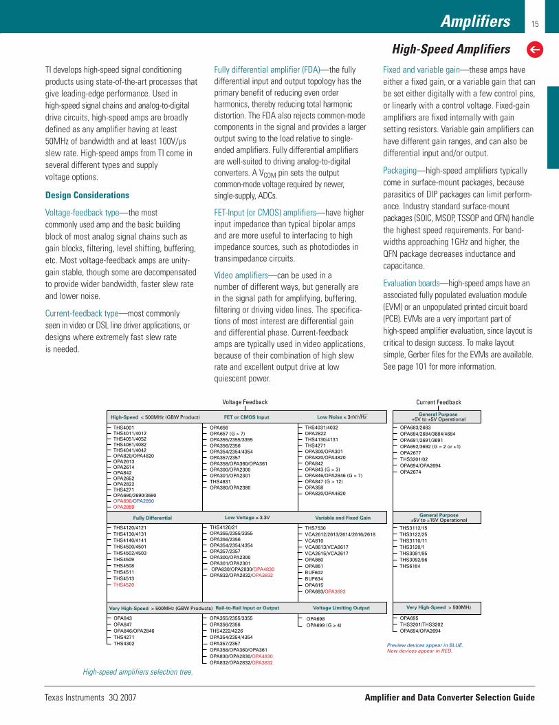
TI develops high-speed signal conditioningproducts using state-of-the-art processes thatgive leading-edge performance. Used in high-speed signal chains and analog-to-digitaldrive circuits, high-speed amps are broadlydefined as any amplifier having at least50MHz of bandwidth and at least 100V/µsslew rate. High-speed amps from TI come inseveral different types and supply voltage options.
Design Considerations
Voltage-feedback type—the most commonly used amp and the basic buildingblock of most analog signal chains such asgain blocks, filtering, level shifting, buffering,etc. Most voltage-feedback amps are unity-gain stable, though some are decompensatedto provide wider bandwidth, faster slew rateand lower noise.
Current-feedback type—most commonly seen in video or DSL line driver applications, ordesigns where extremely fast slew rate is needed.
Fully differential amplifier (FDA)—the fullydifferential input and output topology has theprimary benefit of reducing even order harmonics, thereby reducing total harmonic distortion. The FDA also rejects common-modecomponents in the signal and provides a largeroutput swing to the load relative to single-ended amplifiers. Fully differential amplifiersare well-suited to driving analog-to-digital converters. A VCOM pin sets the output common-mode voltage required by newer, single-supply, ADCs.
FET-Input (or CMOS) amplifiers—have higherinput impedance than typical bipolar ampsand are more useful to interfacing to highimpedance sources, such as photodiodes intransimpedance circuits.
Video amplifiers—can be used in a number of different ways, but generally arein the signal path for amplifying, buffering,filtering or driving video lines. The specifica-tions of most interest are differential gainand differential phase. Current-feedbackamps are typically used in video applications,because of their combination of high slewrate and excellent output drive at low quiescent power.
Fixed and variable gain—these amps haveeither a fixed gain, or a variable gain that canbe set either digitally with a few control pins,or linearly with a control voltage. Fixed-gainamplifiers are fixed internally with gain setting resistors. Variable gain amplifiers canhave different gain ranges, and can also bedifferential input and/or output.
Packaging—high-speed amplifiers typicallycome in surface-mount packages, becauseparasitics of DIP packages can limit perform-ance. Industry standard surface-mount packages (SOIC, MSOP, TSSOP and QFN) handlethe highest speed requirements. For band-widths approaching 1GHz and higher, theQFN package decreases inductance andcapacitance.
Evaluation boards—high-speed amps have anassociated fully populated evaluation module(EVM) or an unpopulated printed circuit board(PCB). EVMs are a very important part of high-speed amplifier evaluation, since layout iscritical to design success. To make layout simple, Gerber files for the EVMs are available.See page 101 for more information.
Preview devices appear in BLUE.New devices appear in RED.
OPA656OPA657 (G > 7)OPA355/2355/3355OPA356/2356OPA354/2354/4354OPA357/2357OPA358/OPA360/OPA361OPA300/OPA2300OPA301/OPA2301THS4631OPA380/OPA2380
THS4031/4032OPA2822THS4130/4131THS4271OPA300/OPA301OPA820/OPA4820OPA842OPA843 (G > 3)OPA846/OPA2846 (G > 7)OPA847 (G > 12)OPA358OPA820/OPA4820
OPA683/2683OPA684/2684/3684/4684OPA691/2691/3691OPA692/3692 (G = 2 or ±1)OPA2677THS3201/02OPA694/OPA2694OPA2674
Voltage Feedback Current Feedback
FET or CMOS Input Low Noise ≤ 3nV/ HzHigh-Speed < 500MHz (GBW Product) General Purpose +5V to ±5V Operational
Voltage Limiting Output
Variable and Fixed Gain
Very High-Speed > 500MHz
Low Voltage ≤ 3.3V General Purpose±5V to ±15V Operational
THS4120/4121THS4130/4131THS4140/4141THS4500/4501THS4502/4503THS4509THS4508THS4511THS4513THS4520
OPA843OPA847OPA846/OPA2846THS4271THS4302
OPA355/2355/3355OPA356/2356THS4222/4226OPA354/2354/4354OPA357/2357OPA358/OPA360/OPA361OPA830/OPA2830/OPA4830OPA832/OPA2832/OPA3832
OPA698OPA699 (G ≥ 4)
OPA695THS3201/THS3202OPA694/OPA2694
THS4120/21OPA355/2355/3355OPA356/2356OPA354/2354/4354OPA357/2357OPA300/OPA2300OPA301/OPA2301 OPA830/OPA2830/OPA4830OPA832/OPA2832/OPA3832
THS7530VCA2612/2613/2614/2616/2618VCA810VCA8613/VCA8617VCA2615/VCA2617OPA860OPA861BUF602BUF634OPA615OPA693/OPA3693
THS3112/15THS3122/25THS3110/11THS3120/1THS3091/95THS3092/96THS6184
Fully Differential
Rail-to-Rail Input or OutputVery High-Speed > 500MHz (GBW Products)
THS4001THS4011/4012THS4051/4052THS4081/4082THS4041/4042OPA820/OPA4820OPA2613OPA2614OPA842OPA2652OPA2822THS4271OPA690/2690/3690OPA890/OPA2890OPA2889
High-speed amplifiers selection tree.
Amplifier and Data Converter Selection Guide Texas Instruments 3Q 2007
Amplifiers
High-Speed Amplifiers
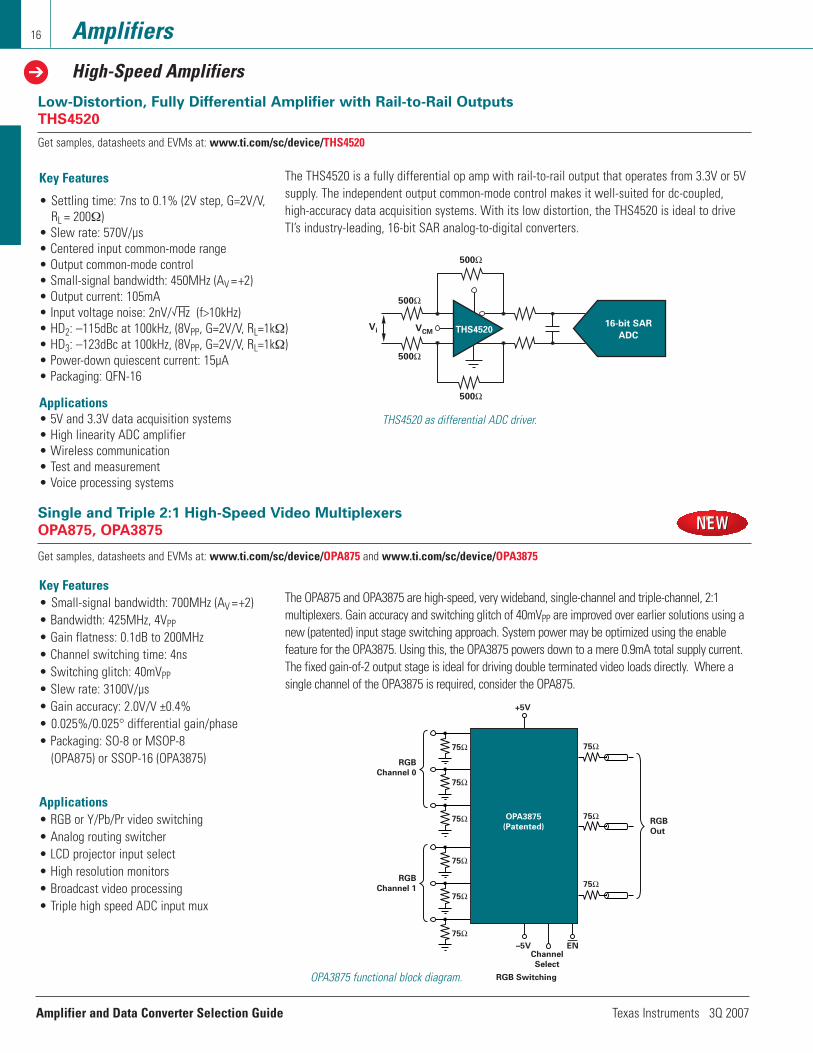
16
THS4520Vi VCM
500Ω
500Ω
500Ω
500Ω
16-bit SAR
ADC
Low-Distortion, Fully Differential Amplifier with Rail-to-Rail Outputs
THS4520
Get samples, datasheets and EVMs at: www.ti.com/sc/device/THS4520
THS4520 as differential ADC driver.
Key Features
• Settling time: 7ns to 0.1% (2V step, G=2V/V,RL = 200Ω)
• Slew rate: 570V/µs • Centered input common-mode range• Output common-mode control• Small-signal bandwidth: 450MHz (AV =+2)• Output current: 105mA • Input voltage noise: 2nV/ Hz (f>10kHz)• HD2: –115dBc at 100kHz, (8VPP, G=2V/V, RL=1kΩ)• HD3: –123dBc at 100kHz, (8VPP, G=2V/V, RL=1kΩ)• Power-down quiescent current: 15µA• Packaging: QFN-16
Applications• 5V and 3.3V data acquisition systems• High linearity ADC amplifier• Wireless communication• Test and measurement• Voice processing systems
The THS4520 is a fully differential op amp with rail-to-rail output that operates from 3.3V or 5Vsupply. The independent output common-mode control makes it well-suited for dc-coupled,high-accuracy data acquisition systems. With its low distortion, the THS4520 is ideal to driveTI’s industry-leading, 16-bit SAR analog-to-digital converters.
+5V
75Ω
75Ω
75Ω
75Ω
75Ω
75Ω–5V EN
OPA3875
(Patented)
75Ω
75Ω
75Ω
RGB
Out
RGB Switching
RGB
Channel 1
RGB
Channel 0
Channel
Select
Single and Triple 2:1 High-Speed Video Multiplexers
OPA875, OPA3875
Get samples, datasheets and EVMs at: www.ti.com/sc/device/OPA875 and www.ti.com/sc/device/OPA3875
OPA3875 functional block diagram.
Key Features• Small-signal bandwidth: 700MHz (AV =+2)• Bandwidth: 425MHz, 4VPP • Gain flatness: 0.1dB to 200MHz• Channel switching time: 4ns• Switching glitch: 40mVPP • Slew rate: 3100V/µs • Gain accuracy: 2.0V/V ±0.4% • 0.025%/0.025° differential gain/phase• Packaging: SO-8 or MSOP-8
(OPA875) or SSOP-16 (OPA3875)
Applications• RGB or Y/Pb/Pr video switching• Analog routing switcher • LCD projector input select• High resolution monitors• Broadcast video processing• Triple high speed ADC input mux
The OPA875 and OPA3875 are high-speed, very wideband, single-channel and triple-channel, 2:1 multiplexers. Gain accuracy and switching glitch of 40mVPP are improved over earlier solutions using anew (patented) input stage switching approach. System power may be optimized using the enable feature for the OPA3875. Using this, the OPA3875 powers down to a mere 0.9mA total supply current.The fixed gain-of-2 output stage is ideal for driving double terminated video loads directly. Where asingle channel of the OPA3875 is required, consider the OPA875.

Texas Instruments 3Q 2007 Amplifier and Data Converter Selection Guide
Amplifiers
High-Speed Amplifiers
17
High
-Spe
ed A
mpl
ifier
s Se
lect
ion
Guid
eDi
storti
onSe
ttlin
g TH
D1V
pp, G
= 2,
I QBW
BWGB
WTim
e2V
pp5M
Hz
Diffe
rent
ial
Per
Supp
lyat
ACL
G = +
2Pr
oduc
tSl
ew
0.1%
G = 1
HD2
HD3
V NV O
SI B
Ch.
I OUT
Volta
geA C
L(M
Hz)
(MHz
)(M
Hz)
Rate
(ns)
1MHz
(dBc
)(d
Bc)
Gain
Phas
e(n
V/ H
z)(m
V)(µ
A)(m
A)(m
A)De
vice
Ch.
SHDN
(V)
(min
)(ty
p)(ty
p)(ty
p)(V
/µs)
(typ)
(dB)
(typ
)(ty
p)(ty
p)(%
)(°)
(typ)
(max
)(m
ax)
(typ)
(typ)
Pack
age(
s)Pr
ice*
Volta
ge F
eedb
ack
(Sor
ted
by A
scen
ding
Gai
n B
andw
idth
Pro
duct
)TH
S405
1/52
1, 2
N±5
, ±15
170
3850
240
60–8
2–6
6–7
90.0
10.0
114
106
8.510
0SO
IC, M
SOP
Powe
rPAD
™$0
.95
THS4
281
1N
+2.7,
±5, +
151
9040
—35
78—
——
0.05
0.25
12.5
300.5
750
30SO
T23-
5, M
SOP,
SOIC
$0.95
OPA2
889
2Y
5, ±5
111
560
7525
025
–74
–76
–79
0.06
0.04
8.45
0.75
0.46
40M
SOP,
SOIC
$1.20
TH
S401
1/12
1, 2
N±5
, ±15
129
050
100
310
37–8
0–6
5–8
00.0
060.0
17.5
66
7.811
0SO
IC, M
SOP
Powe
rPAD
$1.45
TH
S408
1/82
1, 2
N±5
, ±15
117
570
100
230
43–6
4–6
7–5
20.0
10.0
510
76
3.485
SOIC
, MSO
P Po
werP
AD$1
.20
OPAy
354/5
71,
2, 4
Y2.5
to 5.
51
250
9010
015
030
—–7
5–8
30.0
20.0
96.5
850
pA
4.910
0SO
T23,
SOIC
Pow
erPA
D$0
.75
OPAy
890
1, 2
Y5,
±51
275
9212
040
010
–88
–82
–90
0.05
0.03
86
1.62.2
540
MSO
P, SO
IC$0
.80OP
Ay83
01,
2 ,4
N+3
, +5,
±51
310
120
110
600
42–8
2–7
1–7
70.0
70.1
79.5
1.510
4.25
150
SOT2
3, SO
IC$0
.75
THS4
221/2
21,
2N
3, 5,
±5, 1
51
230
100
120
975
25–1
00–7
9–9
20.0
070.0
0713
103
1410
0SO
IC, M
SOP
Powe
rPAD
$1.90
OP
A261
32
N5,
±61
230
110
125
7040
–94
——
——
1.81
106
350
SOIC
, SOI
C Po
werP
AD$1
.55
OPAy
300/3
011
Y2.7
to 5.
51
400
8015
080
30—
–74
–78
0.01
0.13
50.5
1240
SOT2
3, SO
IC$1
.25
OPA8
421
N±5
135
015
020
040
015
–107
–100
–104
0.003
0.008
2.61.2
3520
.210
0SO
T23,
SOIC
$1.55
OP
A265
22
N±5
170
020
020
033
5—
–100
–76
–66
0.05
0.03
87
155.5
140
SOT2
3, SO
IC$1
.15
OPAy
356
1, 2
N2.5
to 5.
51
450
100
200
300
30—
–81
–93
0.02
0.05
5.89
50pA
8.360
SOT2
3, SO
IC, M
SOP
$0.70
OPAy
355
1, 2,
3Y
2.5 to
5.5
145
010
020
030
030
—–8
1–9
30.0
20.0
55.8
950
pA
8.360
SOT2
3, SO
IC, M
SOP,
TSSO
P$0
.70
THS4
031/3
21,
2N
±5, ±
151
275
100
220
100
60–7
2–7
7–6
70.0
150.0
251.6
26
8.590
SOIC
, MSO
P Po
werP
AD$1
.65
OPA2
822
2N
5, ±5
140
020
022
017
032
–96
–81
–91
0.02
0.03
21.2
124.8
150
SOIC
, MSO
P$1
.35
OPA6
561
N±5
140
018
524
029
08
–92
–80
–89
0.01
0.01
62
20pA
2560
SOT2
3, SO
IC$3
.35
OPA6
981
N5,
±51
450
215
250
1100
—–9
3–8
2–8
80.0
120.0
085.6
510
15.5
120
SOIC
$1.90
OP
Ay82
01,
4N
5 to ±
51
800
240
280
240
18–8
4–9
0–1
100.0
10.0
37.5
0.75
175.6
110
SOIC
, SOI
C Po
werP
AD$0
.90
OPA2
614
2N
5, ±6
218
018
029
014
535
–85
–72
–81
——
1.81
14.5
6.535
0SO
IC, S
OIC
Powe
rPAD
$1.55
OP
Ay69
01,
2, 3
Y5,
±51
500
220
300
1800
8–9
1–7
8–7
80.0
60.0
35.5
48
5.519
0SO
T23,
SOIC
, SSO
P$1
.35
THS4
271/7
51
Y5,
±5, 1
51
1400
390
400
1000
25–1
10–1
00–9
40.0
070.0
043
1015
2216
0SO
IC, M
SOP
Powe
rPAD
$2.25
OP
A843
1N
±53
500
—80
010
007.5
–105
——
0.001
0.012
21.2
3520
.210
0SO
T23,
SOIC
$1.60
TH
S430
41
N3 t
o ±5
130
0010
0087
010
005
–92
–92
–75
——
2.44
618
100
SOT2
3, SO
IC, M
SOP
$1.75
OP
A699
1N
5, ±5
426
0—
1000
1400
7—
——
0.012
0.008
4.15
1015
.512
0SO
IC$1
.95
OPA6
571
N±5
735
0—
1600
700
10—
——
——
4.81.8
20pA
1470
SOT2
3, SO
IC$3
.80
OPAy
846
1, 2
N±5
750
0—
1750
625
10—
——
0.02
0.02
1.20.6
1912
.680
SOT2
3, SO
IC$1
.70
OPA8
471
Y±5
1260
0—
3800
950
10—
——
——
0.85
0.539
18.1
75SO
T23,
SOIC
$2.00
Cu
rren
t Fee
dbac
k (S
orte
d by
Asc
endi
ng G
ain
of +
2 B
andw
idth
)TH
S311
0/11
1Y
±5, ±
151
100
90—
1300
27–7
8–6
0–6
10.0
10.0
33
620
4.826
0SO
IC, M
SOP
Powe
rPAD
$1.30
TH
S311
2/15
2Y
±5, ±
151
110
110
—15
5063
–78
–77
–80
0.01
0.011
2.28
234.9
270
SOIC
, SOI
C Po
werP
AD$2
.00
THS3
120/1
1Y
±5, ±
151
130
120
—15
0011
–53
–65
–53
0.007
0.018
2.56
37
475
SOIC
, MSO
P Po
werP
AD$1
.85
THS3
122/2
52
Y±5
, ±15
116
012
8—
1550
64–7
8–7
0–7
70.0
10.0
112.2
623
8.444
0SO
IC, S
OIC
Powe
rPAD
$2
.95
OPAy
683
1, 2
Y5,
±51
200
150
—54
0—
–84
–70
–85
0.06
0.03
4.43.5
40.9
411
0SO
T23,
SOIC
$1.20
OP
Ay68
41, 2
, 3, 4
Y5,
±51
210
160
—82
0—
–77
–73
–77
0.04
0.02
3.73.5
351.7
120
SOT2
3, SO
IC, T
SSOP
$1.35
OP
A267
72
N5,
±61
220
200
—20
00—
–87
–75
–85
0.03
0.01
24.5
430
950
0SO
IC, S
OIC P
ower
PAD,
QFN
$1.65
TH
S309
1/51
Y±5
, ±15
123
521
0—
5000
42–7
2–7
9–8
80.0
130.0
22
315
9.528
0SO
IC, S
OIC
Powe
rPAD
$2.45
* Sugg
este
d re
sale
pric
e in
U.S
. dol
lars
in q
uant
ities
of 1
,000
. N
ew p
rodu
cts
are
liste
d in
bol
d re
d. P
revi
ew p
rodu
cts
are
liste
d in
bol
d bl
ue.

Amplifier and Data Converter Selection Guide Texas Instruments 3Q 2007
Amplifiers
High-Speed Amplifiers
18
High
-Spe
ed A
mpl
ifier
s Se
lect
ion
Guid
eDi
storti
onSe
ttlin
g TH
D1V
pp, G
= 2,
I QBW
BWGB
WTim
e2V
pp5M
Hz
Diffe
rent
ial
Per
Supp
lyat
ACL
G = +
2Pr
oduc
tSl
ew
0.1%
G = 1
HD2
HD3
V NV O
SI B
Ch.
I OUT
Volta
geA C
L(M
Hz)
(MHz
)(M
Hz)
Rate
(ns)
1MHz
(dBc
)(d
Bc)
Gain
Phas
e(n
V/ H
z)(m
V)(µ
A)(m
A)(m
A)De
vice
Ch.
SHDN
(V)
(min
)(ty
p)(ty
p)(ty
p)(V
/µs)
(typ)
(dB)
(typ
)(ty
p)(ty
p)(%
)(°)
(typ)
(max
)(m
ax)
(typ)
(typ)
Pack
age(
s)Pr
ice*
Curr
ent F
eedb
ack
(Sor
ted
by A
scen
ding
Gai
n of
+2
Ban
dwid
th) (
Cont
inue
d)TH
S309
2/62
Y±5
, ±15
123
521
0—
5000
42–7
2–7
9–8
80.0
130.0
22
415
9.528
0SO
IC, S
OIC
Powe
rPAD
™$3
.90
OPA2
674
2Y
5, ±6
125
022
5—
2000
—–8
7–7
3–8
20.0
30.0
12
4.530
950
0SO
IC, S
OIC
Powe
rPAD
$1.70
OP
Ay69
11,
2, 3
Y5,
±51
280
225
—21
008
–93
–77
–79
0.07
0.02
1.72.5
355.1
190
SOT-2
3, SO
IC, S
SOP
$1.45
OP
Ay69
41,
2N
±51
1500
690
—17
0013
—–9
2–9
30.0
30.0
152.1
4.118
5.880
SOT-2
3, SO
IC$1
.25
THS3
201/0
21,
2N
±5, ±
7.51
1800
850
—62
0020
–85
–85
–95
0.006
0.03
1.65
313
1411
5M
SOP,
SOT2
3, SO
IC$1
.60
OPA6
951
Y5,
±51
1700
1400
—43
00—
–86
–88
–95
0.04
0.007
1.83
3012
.912
0SO
T23,
SOIC
$1.35
Fu
lly D
iffer
entia
l Am
plifi
ers
(Sor
ted
by A
scen
ding
Gai
n B
andw
idth
Pro
duct
)TH
S413
0/31
1Y
5, ±5
, ±15
115
090
180
5278
–97
–60
–75
——
1.32
612
.385
SOIC
, MSO
P Po
werP
AD$2
.80
THS4
502/0
31
Y5,
±51
370
175
280
2800
6.3–1
00–8
3–9
7—
—6
74.6
2312
0SO
IC, M
SOP
Powe
rPAD
$4
.00
THS4
520
1Y
3 to 5
160
040
012
0052
07
–100
——
—
—2
2511
1310
5QF
N$2
.45TH
S451
11
Y3,
51
1600
1400
2000
4900
3.3–9
7—
——
—2
5.215
.539
.261
QFN
$3.45
TH
S451
31
Y3,
51
1600
1400
2000
5100
16–9
7—
——
—2.2
5.213
37.7
96QF
N$3
.25
THS4
508
1Y
3, 5
220
0020
0030
0064
002
–98
——
——
2.35
15.5
39.2
61QF
N$3
.95
THS4
509
1Y
3, 5
220
0020
0030
0066
002
–98
——
——
1.95
1337
.796
QFN
$3.75
Fi
xed
and
Vari
able
Gai
n (S
orte
d by
Asc
endi
ng A
CLB
andw
idth
)VC
A810
1N
±50.0
130
30—
350
30–3
5–7
1–3
5—
—2.4
0.25
1020
60SO
IC$5
.75
OPAy
832
1, 2
N2.8
to ±5
190
80—
350
45–6
4–6
6–7
30.1
0.16
9.27
104.2
512
0SO
T23,
SOIC
$0.70
BU
F634
1N
5, ±5
, ±15
118
0—
—20
0020
0—
——
0.40.1
410
020
1525
0SO
IC$3
.05
OPAy
692
1, 3
Y5,
±51
280
225
—20
008
–93
–70
–74
0.07
0.02
1.72.5
355.1
190
SOT2
3, SO
IC, S
SOP
$1.15
TH
S753
01
Y5
430
0—
—17
50—
–51
–54
–50
——
1.27
—30
3520
TSSO
P Po
werP
AD$3
.85
BUF6
021
N3.3
, 5, ±
51
1200
——
8000
——
——
0.15
0.04
5.130
75.8
60SO
T23,S
OIC
$0.85
OP
Ay69
31
Y5,
±51
1400
700
—25
0012
–87
–74
–87
0.03
0.01
1.82
3513
120
SOT2
3, SO
IC$1
.30
THS4
303
1Y
3, 5
1018
00—
—55
00—
——
——
—2.5
4.25
1034
180
MSO
P Po
werP
AD$2
.10
THS4
302
1Y
3, 5
524
00—
—55
00—
——
——
—2.8
4.25
1037
180
MSO
P Po
werP
AD$2
.10
JFET
-Inp
ut a
nd C
MO
S A
mpl
ifier
s(S
orte
d by
Asc
endi
ng G
ain
Ban
dwid
th P
rodu
ct)
OPA3
581
Y2.7
to 3.
31
100
1080
5535
——
—0.3
0.76.4
650
pA7.5
50SC
70$0
.45
OPAy
380
1, 2
N2.7
to 5.
51
100
1090
80—
——
——
—67
0.025
50pA
7.550
MSO
P, SO
IC$1
.95
OPAy
354
1, 2,
4N
2.5 to
5.5
125
090
100
150
30—
–75
–83
0.02
0.09
6.58
50pA
4.9
100
SOT2
3, SO
IC P
ower
PAD
$0.67
OP
Ay35
71,
2Y
2.5 to
5.5
125
090
100
150
30—
–75
–83
0.02
0.09
6.58
50pA
4.9
100
SOT2
3, SO
IC P
ower
PAD
$0.67
OP
Ay30
0/301
1,2Y
2.7 to
5.5
1—
8015
080
30—
–74
–78
0.01
0.13
55p
A12
40SO
T-23,
SOIC
$1.25
OP
Ay35
51,
2, 3
Y2.5
to 5.
51
450
100
200
300
30—
–81
–93
0.02
0.05
5.89
50pA
8.3
60M
SOP
$0.69
OP
Ay35
61,
2N
2.5 to
5.5
145
010
020
030
030
—–8
1–9
30.0
20.0
55.8
950
pA8.3
60SO
T23,
SOIC
$0.69
OP
A656
1N
±51
400
185
240
290
8–9
2–8
0–8
90.0
10.0
16
22p
A25
60SO
T23,
SOIC
$3.35
OP
A657
1N
±57
350
—16
0070
010
–83
–73
–100
——
4.81.8
2pA
1470
SOT2
3, SO
IC$3
.80
xDSL
Dri
vers
and
Rec
eive
rs (S
orte
d by
Asc
endi
ng O
utpu
t Cur
rent
)TH
S403
22
N±5
, ±15
127
510
022
010
060
–72
–77
–67
0.015
0.025
1.62
68.5
90SO
IC, M
SOP
Powe
rPAD
™$2
.60
OPA4
684
4N
+5, ±
61
250
170
—75
0—
–79
–80
–80
0.04
0.02
3.73.5
351.7
120
TSSO
P, SO
IC$3
.30
OPA2
822
2N
5, ±5
140
020
022
017
032
–96
–81
–91
0.02
0.03
21.2
124.8
150
SOIC
, MSO
P$1
.35
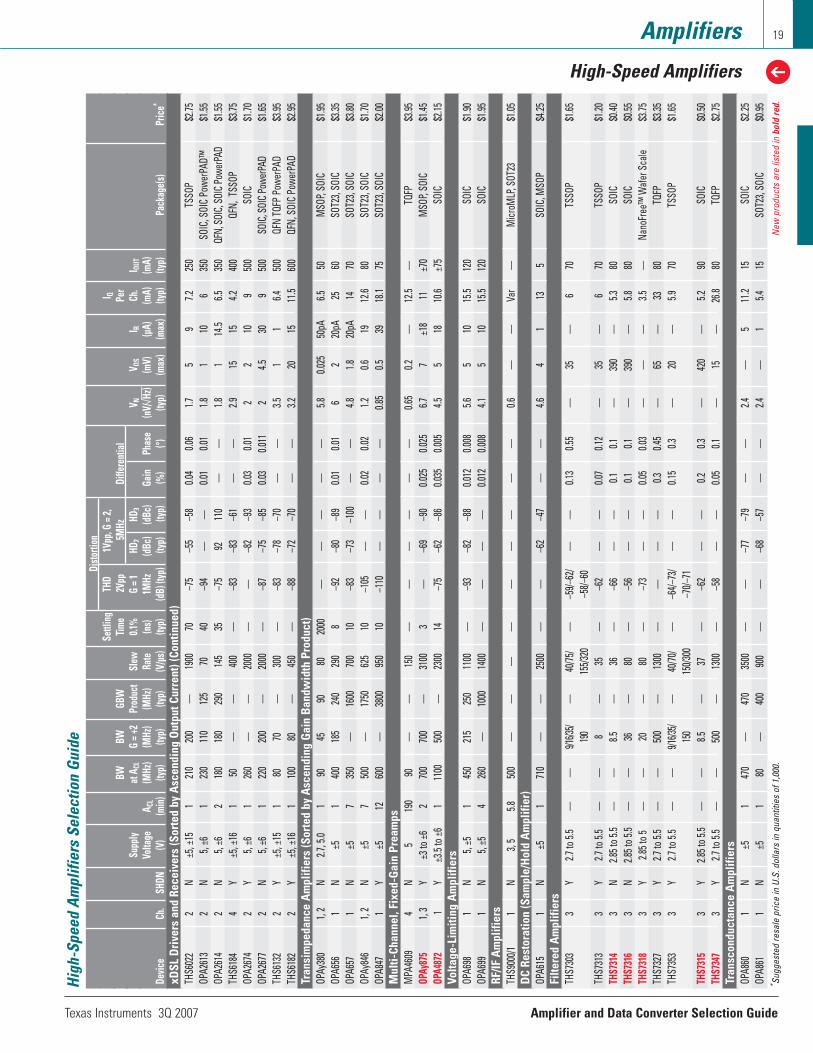
* Sugg
este
d re
sale
pric
e in
U.S
. dol
lars
in q
uant
ities
of 1
,000
. N
ew p
rodu
cts
are
liste
d in
bol
d re
d.
Texas Instruments 3Q 2007 Amplifier and Data Converter Selection Guide
Amplifiers
High-Speed Amplifiers
19
High
-Spe
ed A
mpl
ifier
s Se
lect
ion
Guid
eDi
storti
onSe
ttlin
g TH
D1V
pp, G
= 2,
I QBW
BWGB
WTim
e2V
pp5M
Hz
Diffe
rent
ial
Per
Supp
lyat
ACL
G = +
2Pr
oduc
tSl
ew
0.1%
G = 1
HD2
HD3
V NV O
SI B
Ch.
I OUT
Volta
geA C
L(M
Hz)
(MHz
)(M
Hz)
Rate
(ns)
1MHz
(dBc
)(d
Bc)
Gain
Phas
e(n
V/ H
z)(m
V)(µ
A)(m
A)(m
A)De
vice
Ch.
SHDN
(V)
(min
)(ty
p)(ty
p)(ty
p)(V
/µs)
(typ)
(dB)
(typ
)(ty
p)(ty
p)(%
)(°)
(typ)
(max
)(m
ax)
(typ)
(typ)
Pack
age(
s)Pr
ice*
xDSL
Dri
vers
and
Rec
eive
rs (S
orte
d by
Asc
endi
ng O
utpu
t Cur
rent
)(Co
ntin
ued)
THS6
022
2N
±5, ±
151
210
200
—19
0070
–75
–55
–58
0.04
0.06
1.75
97.2
250
TSSO
P$2
.75
OPA2
613
2N
5, ±6
123
011
012
570
40–9
4—
—0.0
10.0
11.8
110
635
0SO
IC, S
OIC
Powe
rPAD
™$1
.55
OPA2
614
2N
5, ±6
218
018
029
014
535
–75
9211
0—
—1.8
114
.56.5
350
QFN,
SOIC
, SOI
C Pow
erPA
D$1
.55
THS6
184
4Y
±5, ±
161
50—
—40
0—
–83
–83
–61
——
2.915
154.2
400
QFN,
TSS
OP$3
.75
OPA2
674
2Y
5, ±6
126
0—
—20
00—
—–8
2–9
30.0
30.0
12
210
950
0SO
IC$1
.70
OPA2
677
2N
5, ±6
122
020
0—
2000
—–8
7–7
5–8
50.0
30.0
112
4.530
950
0SO
IC, S
OIC P
ower
PAD
$1.65
TH
S613
22
Y±5
, ±15
180
70—
300
—–8
3–7
8–7
0—
—3.5
11
6.450
0QF
N TQ
FP P
ower
PAD
$3.95
TH
S618
22
Y±5
, ±16
110
080
—45
0—
–88
–72
–70
——
3.220
1511
.560
0QF
N, S
OIC
Powe
rPAD
$2
.95
Tran
sim
peda
nce
Am
plifi
ers
(Sor
ted
by A
scen
ding
Gai
n B
andw
idth
Pro
duct
)OP
Ay38
01,
2N
2.7, 5
.01
9045
9080
2000
——
——
—5.8
0.025
50pA
6.550
MSO
P, SO
IC$1
.95
OPA6
561
N±5
140
018
524
029
08
–92
–80
–89
0.01
0.01
62
20pA
2560
SOT2
3, SO
IC$3
.35
OPA6
571
N±5
735
0—
1600
700
10–8
3–7
3–1
00—
—4.8
1.820
pA14
70SO
T23,
SOIC
$3.80
OP
Ay84
61,
2N
±57
500
—17
5062
510
–105
——
0.02
0.02
1.20.6
1912
.680
SOT2
3, SO
IC$1
.70
OPA8
471
Y±5
1260
0—
3800
950
10–1
10—
——
—0.8
50.5
3918
.175
SOT2
3, SO
IC$2
.00
Mul
ti-Ch
anne
l, Fi
xed-
Gai
n Pr
eam
psM
PA46
094
N5
190
90—
—15
0—
——
——
—0.6
50.2
—12
.5—
TQFP
$3.95
OPAy
875
1, 3
Y±3
to ±6
270
070
0—
3100
3—
–69
–90
0.025
0.025
6.77
±18
11±7
0M
SOP,
SOIC
$1.45
OPA4
872
1Y
±3.5
to ±6
111
0050
0 —
2300
14–7
5–6
2–8
60.0
350.0
054.5
518
10.6
±75
SOIC
$2.15
Volta
ge-L
imiti
ng A
mpl
ifier
sOP
A698
1N
5, ±5
145
021
525
011
00—
–93
–82
–88
0.012
0.008
5.65
1015
.512
0SO
IC$1
.90
OPA6
991
N5,
±54
260
—10
0014
00—
——
—0.0
120.0
084.1
510
15.5
120
SOIC
$1.95
RF
/IF A
mpl
ifier
sTH
S900
0/11
N3,
55.8
500
——
——
——
——
—0.6
——
Var
—M
icroM
LP, S
OT23
$1.05
D
C Re
stor
atio
n (S
ampl
e/H
old
Am
plifi
er)
OPA6
151
N±5
171
0—
—25
00—
—–6
2–4
7—
—4.6
41
135
SOIC
, MSO
P$4
.25
Filte
red
Am
plifi
ers
THS7
303
3Y
2.7 to
5.5
——
9/16/3
5/—
40/75
/—
–59/–
62/
——
0.13
0.55
—35
—6
70TS
SOP
$1.65
19
015
5/320
–58/–
60TH
S731
33
Y2.7
to 5.
5—
—8
—35
—–6
2—
—0.0
70.1
2—
35—
670
TSSO
P$1
.20
THS7
314
3N
2.85 t
o 5.5
——
8.5—
36—
–66
——
0.10.1
—39
0—
5.380
SOIC
$0.40
THS7
316
3N
2.85 t
o 5.5
——
36—
80—
–56
——
0.10.1
—39
0—
5.880
SOIC
$0.55
THS7
318
3Y
2.85 t
o 5—
—20
—80
—–7
3—
—0.0
50.0
3—
——
3.5—
Nano
Free
™ W
afer
Sca
le$3
.75TH
S732
73
Y2.7
to 5.
5—
—50
0—
1300
——
——
0.30.4
5—
65—
3380
TQFP
$3.35
THS7
353
3Y
2.7 to
5.5
——
9/16/3
5/—
40/70
/—
–64/–
73/
——
0.15
0.3—
20—
5.970
TSSO
P$1
.65
150
150/3
00–7
0/–71
THS7
315
3Y
2.85 t
o 5.5
——
8.5—
37—
–62
——
0.20.3
—42
0—
5.290
SOIC
$0.50
THS7
347
3Y
2.7 to
5.5
——
500
—13
00—
–58
——
0.05
0.1—
15—
26.8
80TQ
FP$2
.75Tr
ansc
ondu
ctan
ce A
mpl
ifier
sOP
A860
1N
±51
470
—47
035
00—
—–7
7–7
9—
—2.4
—5
11.2
15SO
IC$2
.25OP
A861
1N
±51
80—
400
900
——
–68
–57
——
2.4—
15.4
15SO
T23,
SOIC
$0.95
* Sugg
este
d re
sale
pric
e in
U.S
. dol
lars
in q
uant
ities
of 1
,000
. N
ew p
rodu
cts
are
liste
d in
bol
d re
d.

Amplifier and Data Converter Selection Guide Texas Instruments 3Q 2007
20 Amplifiers
Video Amplifiers
OPAy354 (2.5V to 5.5V)OPAy355 (2.5V to 5.5V)OPAy356 (2.5V to 5.5V)OPAy357 (2.5V to 5.5V)THS4281 (2.7, ±7.5V)OPAy358 (2.7V to 3.3V)OPA360 (2.7V to 3.3V)OPA361 (2.7V to 3.3V)OPAy830 (2.8V, ±5.0) OPAy832 (2.8V, ±5)OPAy690 (5V, ±5V)OPA842 (5V, ±5V)OPAy820 (5V, ±5V)
OPAy694 (±5V)OPAy691 (5V, ±5V)OPAy684 (5V, ±5V)OPAy683 (5V, ±5V)OPAy692 (5V, ±5V)OPAy693 (5V, ±5V)OPAy695 (5V, ±5V)
OPA360 (2.7V to 3.3V)OPA361 (2.5V to 3.3V)THS7303 (2.7V to 5.5V)THS7313 (2.7V to 5.5V)THS7353 (2.7V to 5.5V)THS7327 (2.7V to 5.5V)THS7314 (2.85V to 5.5V)THS7315 (2.85V to 5.5V)THS7316 (2.85V to 5.5V)THS7318 (2.85V to 5V)THS7347 (2.7V to 5.5V)
OPA615 (±5V)BUF602 (±5V, +5V, +3.3V)OPA861 (±5V)OPAy875 (±5V)OPA4872 (±5V)
Video Amplifiers
Current Feedback Filtered Amplifiers Special FunctionsVoltage Feedback
New devices appear in RED.
rail-to-rail output that swings within 100mV ofthe rails to allow for either AC or DC-coupling.The THS7347 incorporates a 500MHz band-width, 1200V/µs unity-gain buffer making itideal for driving ADCs and video decoders,where the THS7327 offers an integrated 5thorder Butterworth anti-aliasing filter on eachchannel. These filters improve image qualityby eliminating DAC images.
Portable Video— Successfully designing ahigh-performance video system into low voltage portable applications requires carefulattention to many details. Portable applications impose very challenging technicalrequirements beyond those required in typicalvideo applications and demand particulartrade-offs in performance, power consumption,printed circuit board space and cost. A DC-coupled solution with integrated gain, low-pass filter, level-shifter, and shutdownsolves these challenges while maintaininggood video performance and eliminates theneed for large, expensive discrete components.The standard definition (SDTV) THS7314 andhigh definition (HDTV) THS7316 easily meetthese trade-offs by maintaining outstandinglow-cost performance while the EDTV/SDTVline driver THS7318, with it’s small profilewafer scale package, is ideal for extremelyboard space sensitive applications.
The new low power THS7315 is a fully-integrated SDTV video amplifier which featuresa rail-to-rail output stage allowing for both ACand DC line driving. The low 15.6mA quiescentcurrent at 3.3V makes it an excellent choice forUSB powered or other power sensitive videoapplications.
Video amplifiers—can be used in a numberof different ways, but generally are in the signal path for amplifying, buffering, filtering ordriving video lines. The specifications of mostinterest for composite video signals, or CVBS,are differential gain and differential phase. Forother video signals, such as Y’P’bP’r or RGB,bandwidth – both small signal and large signal, and slew rate are of most importance.Noise and DC accuracy is also consideredimportant in some high-end applications.
The traditional Voltage-Feedback (VFB) ampli-fiers are widely used because of their ability tobe configured for almost any situation. ManyVFB amplifiers have the ability to accept inputsignals going to the negative rail (or ground),allowing use in many single-supply systems.Additionally, many VFB amplifiers offer rail-to-rail outputs offering the widest dynamic rangepossible on small supplies. Traditional VFBamplifiers (non-RRO) designed for video offerthe ability to have very high slew rates, widebandwidths, low noise, and very good DC characteristics. Current-feedback amps arecommonly found in high-end video applications,because of their combination of high slew rateand excellent output drive at low quiescent power.
High-Speed Video Multiplexers—Numerous video applications, such as RGB orYPbPr video switching, video routers, high resolution monitors, etc. are creating anincreased need for high-speed switching withmultiplexers (muxes). With the increased needto reduce board space are also the demandsthat these muxes provide low power consumption as well as increased functionality,such as the ability to drive 75-Ohms or 150-Ohms while maintaining good video
performance specifications. These specifications include low crosstalk, fast settling, gain flatness, low switching glitchalong with low differential gain and differentialphase. The new OPA875 and OPA3875 single-and triple 2:1 multiplexers along with the newOPA4872, 4:1 multiplexer easily meets theserequirements. Using a new patented inputstage switching approach, the switching glitchis much improved over earlier solutions. Thistechnique uses current steering as the inputswitch while maintaining an overall closed-loop design.
TI brought new technology to the market withthe introduction of the THS7303, THS7313 andTHS7353. These three-channel devices werethe first to offer full I2C programmability of allfunctions independently for each channel,which provides the designer the flexibility toconfigure a video system as required or on-the-fly, without the need for hardware upgrades ormodifications. The devices are designed withintegrated Butterworth filters to provide all theanalog signal conditioning required in videoapplications such as set-top boxes, digital televisions, personal video recorders/DVDreaders and portable USB devices. These highlyintegrated devices provide space savings as aresult of the high levels of integration andadvanced package technology.
The strong combination of integrated featuresand optimized design make TI’s THS7327 andnew THS7347, well suited for use in projectorsand professional video systems. Both 3-channel RGBHV video buffers offer a monitorpass-thru amplifier, unity gain buffer, 2:1 inputmux, I2C control of all functions on each channel, HV synch paths with AdjustableSchmitt Trigger, selectable bias modes and

Texas Instruments 3Q 2007 Amplifier and Data Converter Selection Guide
Amplifiers
Video Amplifiers
21
Input 1
Input 2
0.1µFIn A
In B2:1
0.1µF DC
+ Offset DC
AC-
Bias
AC
Sync
TIP
Clamp
Bypass
9/16/35/75MHz
LPF
Disable = Open
1k 878
3.3V
SDA SCL
Out
0.1µF
47µF
33µF
SAG
75
MonitorOutput
75
3.3V
ADC
675
150
X1
75
75
Ω
Ω
Ω
Ω
Ω
Ω
ΩΩ
3-Channel RGBHV Video Buffer with I2C Control
THS7327
Get samples, datasheets and evaluation modules at: www.ti.com/sc/device/THS7327
3.3V single-supply AC-input/AC-video output system w/SAG correction (1 of 3 channels shown).
Key Features• Three video amplifiers for CVBS, S-Video,
EDTV, HDTV and RGB• HV sync paths with adjustable
Schmitt Trigger• 2:1 input MUX• I2C control of all functions/all channels• Integrated low-pass filters on ADC
buffer path• Selectable input bias modes• Monitor pass-through function
Applications• Projectors• Digital TVs• Professional video systems• Set-top boxes• DLP® projectors/televisions
The THS7327 integrates three analog video channels and two digital channels for HV sync, simplifying system design and reducing component count. The three analog channels incorporate unity gain buffering and monitor feed-through paths to handle all standard videoformats, including RGB, YPbPr and CVBS. The amplifier’s I2C control provides easy system configuration and flexibility with programmable functions that include: integrated 2:1 input multiplexers which enable switching of multiple video sources; fifth-order anti-aliasing filtersenable use with multiple video standards; and input bias modes.
500Ω
500Ω
500Ω
DAC/Encoder
(DaVinci)CVBS
SDTV
CVBS
S-Video Y’
S-Video C’
4801/5761
Y’P’ P’
G’B’R’
Y’
C’B R
+1.8V
+3.3V
1
2
3
3
O
CH.1
CH.2
CH.3
V
75Ω
IN
IN
IN
IN
CH.1 OUT
OUTCH.2
CH.3
GRN
OUT
8
7
6
5
THS7315
GAIN =5.2V/V
75Ω
S-Video
75Ω
OUTY’
OUTC’
75Ω 75Ω
75Ω
OUTCVBS
3-Channel SDTV Buffer with 5th-Order, Low-Pass Filter Compatible with DaVinci™ Processors
THS7315
Get samples, datasheets, evaluation modules and app reports at: www.ti.com/sc/device/THS7315
3.3V single-supply DaVinci™ interface with DC output coupled video line driver.
Key Features• 5-pole Butterworth low-pass filter
at 8.5MHz• Flexible input configuration• Gain of 5.2V/V (14.3dB) compatible with
DaVinci™, DM2xx, DM3xx, DM4xx and OMAP™ processors
• Low total quiescent current: 15.6mA at 3.3V
• Rail-to-rail output swings within 100mV from the rails
Applications• Set-top-box DAC output buffering• DVDR/PVR DAC output buffering• Portable/USB powered systems
THS7315 is a low-power, single-supply (3V to 5V), 3-channel integrated video buffer. It incorporates a fifth-order Butterworth filter which can be used as a DAC reconstruction filter oran ADC anti-aliasing filter. The 8.5MHz filter is a perfect choice for SDTV video which includesComposite (CVBS), S-Video, Y’U’V’, G’B’R’(R’G’B’), and Y’P’BP’R 480i/576i. Its rail-to-rail outputstage allows for both AC and DC line driving.
THS7327
THS7315
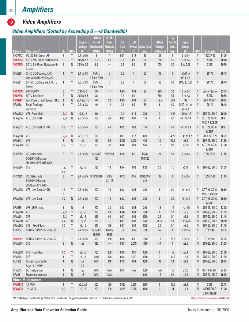
Amplifier and Data Converter Selection Guide Texas Instruments 3Q 2007
Amplifiers
Video Amplifiers
22
Video Amplifiers (Sorted by Ascending G = +2 Bandwidth)–3dB at 0.1dB IQ
Supply G = +2 Gain Diff Diff Offset Per Ch. Input Voltage Bandwidth Flatness Gain Phase Slew Rate Voltage (mA) Range
Device Description1 Ch. SHDN (V) (MHz) (MHz) (%) (°) (V/µs) (mV) (max) (typ) (V) RRO Package(s) Price*
THS7313 I2C, SD 5th-Order LPF 3 Y 2.7 to 5.5 8 4 0.07 0.12 35 35 6 0 to 2.4 Y TSSOP-20 $1.20 THS7314 SDTV, 5th-Order Butterworth 3 Y 2.85 to 5.5 8.5 4.2 0.1 0.1 36 390 5.3 0 to 2.4 Y SOIC $0.40 THS7315 SDTV, 5th Order Butterworth, 3 N 2.85 to 5.5 8.5 — 0.2 0.3 37 420 5.2 0 to 0.56 Y SOIC $0.50
G = 5.2OPA360 G = 2, DC-Coupled, LPF, 1 Y 2.7 to 3.3 9MHz 5 0.5 1 55 80 6 GND to Y SC-70 $0.49
Use with DM270/275/320 2-Pole Filter (V+)–1.5OPA361 G = 5.2, DC-Coupled, LPF, TV 1 Y 2.5 to 3.3 9MHz 5 0.5 1 55 55 5.3 GND to 0.55 Y SC-70 $0.49
Detect 2-Pole FilterTHS7318 EDTV/SDTV 3 Y 2.85 to 5 20 11 0.05 0.03 80 200 3.5 0 to 2.4 Y Wafer Scale $3.75THS7316 HDTV, 5th Order 3 N 2.85 to 5.5 36 — 0.1 0.1 — 390 5.8 0 to 2.3 Y SOIC $0.55THS4281 Low Power, High Speed, RRIO 1 N +2.7, ±5, +15 40 20 0.05 0.08 35 12.5 750 30 Y SOT, MSOP $0.95OPA358 Small Package, 1 Y 2.7 to 3.3 40 12 0.3 0.7 55 6 5.2 GND –0.1 to Y SC-70 $0.45
Low Cost (V+)–1OPAy832 VFB, Fixed Gain 1, 2, 3 N +2.8, ±5 80 — 0.1 0.16 350 7 4.25 –0.5 to 1.5 Y SOT-23, SOIC $0.70 OPAy354 VFB, Low Cost 1, 2, 4 N 2.5 to 5.5 100 40 0.02 0.09 150 8 4.9 –0.1 to 5.4 Y SOT-23, SOIC, $0.67
MSOP, TSSOPOPAy357 VFB, Low Cost, SHDN 1, 2 Y 2.5 to 5.5 100 40 0.02 0.09 150 8 4.9 –0.1 to 5.4 Y SOT-23, SOIC, $0.67
MSOPOPAy830 VFB 1, 2, 4 N +2.8, ±5.5 110 — 0.07 0.17 600 7 4.25 –0.45 to 1.2 Y SO-8, SOT-23 $0.75 OPA842 VFB 1 N ±5 150 56 0.003 0.008 400 1.2 20.2 ±3.2 N SOT-23, SOIC $1.55 OPAy683 CFB 1, 2 Y ±5, +5 150 37 0.06 0.03 540 1.5 0.9 ±3.75 N SOT-23, SOIC, $1.20
MSOPTHS7353 I2C, Selectable 3 Y 2.7 to 5.5 9/16/35/ 5/9/20/25 0.15 0.3 40/70/ 20 5.9 0 to 3.4 Y TSSOP-20 $1.65
SD/ED/HD/Bypass 150 150/3005th-Order LPF, 0dB Gain
OPAy684 CFB 1, 2, Y ±5, +5 160 19 0.04 0.02 820 3.5 1.7 ±3.75 N SOT-23, SOIC $1.353, 4
THS7303 I2C, Selectable 3 Y 2.7 to 5.5 9/16/35/190 5/9.5/ 0.13 0.55 40/75/155/ 35 6 0 to 2.4 Y TSSOP-20 $1.65 SD/ED/HD/Bypass 22/125 3205th-Order LPF, 6dB
OPAy355 VFB, Low Cost, SHDN 1, 2, Y 2.5 to 5.5 200 75 0.02 0.05 300 9 8.3 –0.1 to 3 Y SOT-23, SOIC, $0.69 3 MSOP, TSSOP
OPAy356 VFB, Low Cost 1, 2 N 2.5 to 5.5 200 75 0.02 0.05 300 9 8.3 –0.1 to 3 Y SOT-23, SOIC, $0.69 MSOP
OPA656 VFB, JFET-Input 1 N ±5 200 30 0.02 0.05 290 1.8 14 –4/+2.5 N SOT-23, SOIC $3.35 OPAy690 VFB 1, 2, 3 Y ±5, +5 220 30 0.06 0.03 1800 4 5.5 ±3.5 N SOT-23, SOIC $1.35 OPAy691 CFB 1, 2, 3 Y ±5, +5 225 90 0.07 0.02 2100 2.5 5.1 ±3.5 N SOT-23, SOIC $1.45 OPAy820 VFB 1, 4 N ±.5, ±5 230 — 0.01 0.03 240 0.75 5.6 0.9 to 4.5 N SOT-23, SOIC $0.90 OPAy692 CFB1, Fixed Gain 1, 3 Y ±5, +5 240 120 0.07 0.02 2000 2.5 5.1 ±3.5 N SOT-23, SOIC $1.15 THS7327 RGBHV Buffer, I2C, 2:1MUX 3 Y 2.7 to 5.5 9/16/35/ 4/7/15/ 0.3 0.45 1300 65 33 0 to 2.4 Y TQFP-48 $3.35
75/500 38/56THS7347 RGBHV Buffer, I2C, 2:1MUX 3 Y 2.7 to 5.5 500 350 0.05 0.1 1300 15 26.8 0 to 2.4 Y TQFP-48 $2.75OPAy694 CFB 2 N ±5 690 — 0.03 0.015 1700 4.1 5 ±2.5 N SOT-23, SOIC $1.25
OPAy693 CFB, Fixed Gain 1, 3 Y ±5, +5 700 200 0.03 0.01 2500 2 13 ±3.4 N SOT-23, SOIC $1.30 OPA695 CFB 1 Y ±5, +5 1400 320 0.04 0.007 4300 3 12.9 ±3.3 N SOT-23, SOIC $1.35 BUF602 Closed-Loop Buffer 1 N ±5, N/A 240 0.15 0.04 8000 30 5.8 ±4.0 N SOT-23, SOIC $0.85
AV = ±1, 1.4GHz 3.3OPA615 DC Restoration 1 N ±5 N/A N/A N/A N/A 2500 N/A 13 ± 3.5 N SO-14, MSOP $4.25 OPA861 Transconductance 1 N ±5 N/A N/A — — 900 12 5.4 ±4.2 N SOT-23, SOIC $0.95 Video MultiplexersOPA4872 4:1 MUX 1 Y ±3.5, ±6 500 120 0.035 0.005 2300 5 10.6 ±2.8 N SOIC $2.15OPAy875 2:1 MUX 1, 3 Y ±3, ±6 700 200 0.025 0.025 3100 7 11 ±2.8 N MSOP,SOIC $1.20
SSOP, QSOP 1VFB (Voltage Feedback), CFB (Current Feedback) *Suggested resale price in U.S. dollars in quantities of 1,000 New products are listed in bold red.

Texas Instruments 3Q 2007 Amplifier and Data Converter Selection Guide
Amplifiers
Comparators
23
Comparator ICs are specialized op ampsdesigned to compare two input voltages andprovide a logic state output. They can beconsidered one-bit analog-to-digitalconverters.
The TI comparator portfolio consists of a variety of products with various performancecharacteristics, including: fast ns responsetime, wide input voltage ranges, extremelylow quiescent current consumption and opamp and comparator combination ICs.
Comparator vs. Op AmpComparator Op Amp
Speed (Response time) Yes NoLogic Output Yes NoWide Diff. Input Range Yes YesLow Offset Drift No Yes
In general, if a fast response time is required,use a comparator.
Design ConsiderationsOutput topology• Open collector—connects to the logic
supply through a pull-up resistor and allows comparators to interface to a variety of logic families.
• Push-pull—does not require a pull-up resistor. Because the output swings rail-to-rail, the logic level is dependent on the voltage supplies of the comparator.
Response time (propagation delay)—applications requiring “near real-time” signal response should consider comparatorswith nanosecond (ns) propagation delay. Notethat as propagation delay decreases, supply current increases. Evaluate what mix of performance and power can be afforded. TheTLV349x family offers a unique combinationof speed/power with 5µs propagation delayon only 1µA of quiescent current.
Combination comparator and op amp—forinput signals requiring DC level shifting and/or
gain prior to the comparator, consider theTLV230x (open drain) or TLV270x (push-pull) opamp and comparator combinations. These dualfunction devices save space and cost.
Comparator and voltage reference—comparators typically require a referencevoltage to compare against. The TLV3011 is an integrated comparator and voltage reference combination in a space-savingSC70 package.
Supply Voltage (V)
Re
sp
on
se
Tim
e L
ow
-to
-Hig
h (
µs)
1.81.4
80
36
7
1
1.1
0.3
0.2
0.115
0.0078
0.006
0.025
3.3 5 16 30
TLV3701, TLV3702, TLV3704
TLC3702, TLC3704
TLV3491, TLV3492
TLV3401, TLV3402, TLV3404
TLC393, TLC339
LM393, LM339
LMV331, LMV393, LMV339
TLC372, TLC374
LM211
TL3016
TL714
TL712
Push-Pull Output
Open-Drain Output
TLC352, TLC354
S, 12mA/ch
S, 12.5mA/ch
S, 20mA/ch
S, 6mA/ch
D, Q, 150µA/ch
D, Q, 150µA/ch
S, D, Q, 100µA/ch
D, Q, 500µA/ch
D, Q, 20µA/ch
D, Q, 20µA/ch
S, D, Q, 1.2µA/ch
S, D, Q, 0.8µA/ch
S, D, Q, 0.55µA/ch
Slo
we
rF
aste
r
Incre
asin
g S
pe
ed
TLV3501 S, 12mA/ch
PROPAGATION DELAY vs. OVERDRIVE VOLTAGE
Pro
pag
ati
on
Dela
y (
ns)
Rise
Fall
VCM = 1V
VS = 5V
CLOAD = 17pF
0 20 40 60 80 100
9
8
7
6
5
4
3
Overdrive Voltage (mV)
TLV3501 performance characteristics.
High-Speed Comparator in SOT23TLV3501
Get samples and datasheets at: www.ti.com/sc/device/TLV3501
Key Features• High speed: 4.5ns response at 20mV
overdrive• Beyond-the-rail common-mode input range• Rail-to-rail, push-pull output• Single-supply operation: 2.7V to 5.5V• Packaging: SOT23
Applications• Test and measurement• Power supply monitoring• Base stations
The TLV3501 is a high-speed comparator in a small SOT23 package. Designed for a variety ofapplications, TLV3501 offers very fast response relative to power consumption. It is specifiedover the extended temperature range of –40°C to +125°C.
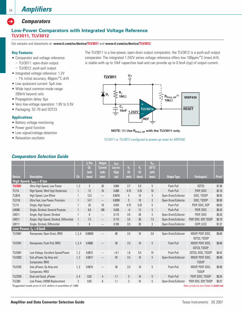
Amplifier and Data Converter Selection Guide Texas Instruments 3Q 2007
Amplifiers
Comparators
24
V+
TLV301xC1
10nF
DI
R1
1MΩ RPULL-UP(1)
10kΩ
RESET
MSP430
1.242V
REF
NOTE: (1) Use RPULL-UP with the TLV3011 only.
TLV3011 or TLV3012 configured to power-up reset for MSP430.
Low-Power Comparators with Integrated Voltage ReferenceTLV3011, TLV3012
Get samples and datasheets at: www.ti.com/sc/device/TLV3011 and www.ti.com/sc/device/TLV3012
Key Features• Comparator and voltage reference:
•• TLV3011: open-drain output•• TLV3012: push-pull output
• Integrated voltage reference: 1.2V•• 1% initial accuracy, 40ppm/°C drift
• Low quiescent current: 5µA max• Wide input common-mode range:
200mV beyond rails• Propagation delay: 6µs• Very low-voltage operation: 1.8V to 5.5V• Packaging: SC-70 and SOT23
Applications• Battery voltage monitoring• Power good function• Low signal/voltage detection• Relaxation oscillator
The TLV3011 is a low-power, open-drain output comparator; the TLV3012 is a push-pull outputcomparator. The integrated 1.242V series voltage reference offers low 100ppm/°C (max) drift, is stable with up to 10nF capacitive load and can provide up to 0.5mA (typ) of output current.
Comparators Selection GuideIQ Per Output tRESP VOS
Ch. Current Low-to- VS VS (25°C)(mA) (mA) High (V) (V) (mV)
Device Description Ch. (max) (min) (µs) (min) (max) (max) Output Type Package(s) Price*High Speed, tRESP ≤ 0.1µsTLV3501 Ultra-High Speed, Low Power 1, 2 5 20 0.004 2.7 5.5 5 Push-Pull SOT23 $1.50 TL714 High Speed, 10mV (typ) Hysteresis 1 12 16 0.006 4.75 5.25 10 Push-Pull PDIP, SOIC $2.16 TL3016 High Speed, Low Offset 1 12.5 — 0.0078 5 10 3 Open-Drain/Collector SOIC, TSSOP $0.95 TL3116 Ultra Fast, Low Power, Precision 1 14.7 — 0.0099 5 10 3 Open-Drain/Collector SOIC, TSSOP $0.95 TL712 Single, High Speed 1 20 16 0.025 4.75 5.25 5 Push-Pull PDIP, SOIC, SOP $0.83 LM306 Single, Strobed, General Purpose 1 6.8 100 0.028 –6 12 5 Push-Pull PDIP, SOIC $0.42 LM211 Single, High Speed, Strobed 1 6 — 0.115 3.5 30 3 Open-Drain/Collector PDIP, SOIC $0.20 LM311 Single, High Speed, Strobed, Differential 1 7.5 — 0.115 3.5 30 7.5 Open-Drain/Collector PDIP, SOIC, SOP, TSSOP $0.18 LM111 Single, Strobed, Differential 1 6 — 0.165 3.5 30 3 Open-Drain/Collector CDIP, LCCC $1.37 Low Power, IQ < 0.5mATLV3401 Nanopower, Open-Drain, RRIO 1, 2, 4 0.00055 — 80 2.5 16 3.6 Open-Drain/Collector MSOP, PDIP, SOIC, $0.60
SOT23, TSSOPTLV3701 Nanopower, Push-Pull, RRIO 1, 2, 4 0.0008 — 36 2.5 16 5 Push-Pull MSOP, PDIP, SOIC, $0.60
SOT23, TSSOPTLV3491 Low Voltage, Excellent Speed/Power 1, 2 0.0012 — < 0.1 1.8 5.5 15 Push-Pull SOT23, SOIC, TSSOP $0.42 TLV2302 Sub-µPower, Op Amp and 1, 2 0.0017 — 55 2.5 16 5 Open-Drain/Collector MSOP, PDIP, SOIC, $0.90
Comparator, RRIO TSSOPTLV2702 Sub-µPower, Op Amp and 1, 2 0.0019 — 36 2.5 16 5 Push-Pull MSOP, PDIP, SOIC, $0.90
Comparator, RRIO TSSOPTLC3702 Dual and Quad, µPower 2, 4 0.02 4 1.1 3 16 5 Push-Pull PDIP, SOIC, TSSOP $0.34 TLC393 Low Power, LM393 Replacement 2 0.02 6 1.1 3 16 5 Open-Drain/Collector PDIP, SOIC, SOP, TSSOP $0.37
*Suggested resale price in U.S. dollars in quantities of 1,000. New products are listed in bold red.
TLV3011

Texas Instruments 3Q 2007 Amplifier and Data Converter Selection Guide
Amplifiers
Comparators Selection Guide (Continued)
25
IQ Per Output tRESP VOS
Ch. Current Low-to- VS VS (25°C)(mA) (mA) High (V) (V) (mV)
Device Description Ch. (max) (min) (µs) (min) (max) (max) Output Type Package(s) Price*Low Power, IQ < 0.5mA (Continued)TLC339 Quad, Low Power 4 0.02 6 1 3 16 5 Open-Drain/Collector PDIP, SOIC, TSSOP $0.44 LP2901 Quad, Low Power, General Purpose 4 0.025 — 1.3 5 30 5 Open-Drain/Collector PDIP, SOIC $0.56 LP339 Quad, Low Power, General Purpose 4 0.025 — 1.3 5 30 5 Open-Drain/Collector PDIP, SOIC $0.49 LMV393 Dual, Low Voltage 2 0.1 10 0.2 2.7 5.5 7 Open-Drain/Collector SOIC, TSSOP $0.34 LMV339 Quad, Low Voltage 4 0.1 — 0.2 2.7 5.5 7 Open-Drain/Collector SOIC, TSSOP $0.36 LMV331 Single, Low Voltage 1 0.12 10 0.2 2.7 5.5 7 Open-Drain/Collector SC70, SOT23 $0.34 TLC372 Fast, Low Power 2, 4 0.15 6 0.2 2 18 5 Open-Drain/Collector PDIP, SOIC, TSSOP $0.33 TLM3302 Quad, General Purpose 4 0.2 6 0.3 2 28 20 Open-Drain/Collector PDIP, SOIC $0.46 LP211 Single, Strobed, Low Power 1 0.3 — 1.2 3.5 30 7.5 Open-Drain/Collector SOIC $0.50 LP311 Single, Strobed, Low Power 1 0.3 1.6 1.2 3.5 30 7.5 Open-Drain/Collector PDIP, SOIC, SOP $0.46 Low Voltage, VS ≤ 2.7V (min)TLC352 1.4V 2, 4 0.15 6 0.2 1.4 18 5 Open-Drain/Collector PDIP, SOIC, TSSOP $0.40 TLV3491 Low Voltage, Excellent Speed/Power 1, 2, 4 0.0012 — < 0.1 1.8 5.5 15 Push-Pull SOT23, SOIC, TSSOP $0.42 TLV2352 Low Voltage 2, 4 0.125 6 0.2 2 8 5 Open-Drain/Collector PDIP, SOIC, TSSOP $0.90 TLC372 Fast, Low Power 2 0.15 6 0.2 2 18 5 Open-Drain/Collector PDIP, SOIC, TSSOP $0.33 LM3302 Quad, General Purpose 4 0.2 6 0.3 2 28 20 Open-Drain/Collector PDIP, SOIC $0.46 LM2903 Dual, General Purpose 2 0.5 6 0.3 2 30 7 Open-Drain/Collector PDIP, SOIC, SOP, TSSOP $0.22 LM293 Dual, General Purpose 2 0.5 6 0.3 2 30 5 Open-Drain/Collector PDIP, SOIC $0.28 LM293A Dual, General Purpose 2 0.5 6 0.3 2 30 3 Open-Drain/Collector SOIC $0.36 LM393 Dual, General Purpose 2 0.5 6 0.3 2 30 5 Open-Drain/Collector PDIP, SOIC, SOP, TSSOP $0.18 LM393A Dual, General Purpose 2 0.5 6 0.3 2 30 3 Open-Drain/Collector PDIP, SOIC, SOP, TSSOP $0.27 LM239 Quad, General Purpose 4 0.5 6 0.3 2 30 5 Open-Drain/Collector PDIP, SOIC $0.28 LM239A Quad, General Purpose 4 0.5 6 0.3 2 30 2 Open-Drain/Collector SOIC $0.91 LM2901 Quad, General Purpose 4 0.625 6 0.3 2 30 3 Open-Drain/Collector PDIP, SOIC, SOP, TSSOP $0.22 LM339 Quad, General Purpose 4 0.5 6 0.3 2 30 5 Open-Drain/Collector PDIP, SOIC, SOP, $0.18
SSOP, TSSOPLM339A Quad, General Purpose 4 0.5 6 0.3 2 30 3 Open-Drain/Collector PDIP, SOIC, SOP $0.27 TL331 Single, Differential 1 0.7 6 0.3 2 36 5 Open-Drain/Collector SOT23 $0.28 LM139 Quad 4 0.5 6 0.3 2 36 5 Open-Drain/Collector SOIC $0.54 LM139A Quad 4 0.5 6 0.3 2 36 2 Open-Drain/Collector SOIC $0.94 LM193 Dual 4 0.5 6 0.3 2 36 5 Open-Drain/Collector SOIC $0.30 TLV3401 Nanopower, RRIO 1, 2, 4 0.00055 — 80 2.5 16 3.6 Open-Drain/Collector MSOP, PDIP, SOIC, $0.60
SOT23, TSSOPTLV3701 Nanopower, RRIO 1, 2, 4 0.0008 — 36 2.5 16 5 Push-Pull MSOP, PDIP, SOIC, $0.60
SOT23, TSSOPLMV331 Single, Low Voltage 1 0.12 10 0.2 2.7 5.5 7 Open-Drain/Collector SC70, SOT23 $0.34 LMV393 Dual, Low Voltage 2 0.1 10 0.2 2.7 5.5 7 Open-Drain/Collector SOIC, TSSOP $0.34 LMV339 Quad Low-Voltage 4 0.1 — 0.2 2.7 5.5 7 Open-Drain/Collector SOIC, TSSOP $0.36 Combination Comparator and Op AmpTLV2302 Sub-µPower, Op Amp and 2 0.0017 — 55 2.5 16 5 Open-Drain/Collector MSOP, PDIP, SOIC, $0.90
Comparator, RRIO TSSOPTLV2702 Sub-µPower, Op Amp and 2, 4 0.0019 — 36 2.5 16 5 Push-Pull MSOP, PDIP, SOIC, $0.90
Comparator, RRIO TSSOPComparator and Voltage ReferenceTLV3011 µPower, Comparator 1 0.003 5 6 1.8 5.5 15 Open-Drain/Collector SC-70, SOT23 $0.75
with 1.242V ReferenceTLV3012 µPower, Comparator 1 0.003 5 6 1.8 5.5 15 Push-Pull SC-70, SOT23 $0.75
with 1.242V Reference*Suggested resale price in U.S. dollars in quantities of 1,000.
Amplifier and Data Converter Selection Guide Texas Instruments 3Q 2007
26 Amplifiers
Difference Amplifiers
Common-mode input voltage range—selection of the most suitable difference ampbegins with an understanding of the inputvoltage range. Some offer resistor networksthat divide down the input voltages, allowing operation with input signals that exceed thepower supplies. A five-resistor version of thesimple difference amplifier results in a devicethat can operate with very high levels ofcommon-mode voltage—far beyond the supply rails.
Gain—signal amplification needed for thedesired circuit function must be considered.With the uncommitted on-chip op amp, theINA145 and the INA146 can be configured forgains of 0.1 to 1000.
Sensor impedance—should be <0.001 of difference amp input impedance to retainCMR and gain accuracy. In other words, theamp input impedance should be 1,000 timeshigher than the source impedance.
Offset voltage drift (µV/°C)—input offsetvoltage changes over temperature. This ismore critical in applications with changingambient temperature.
Quiescent current—often of high importancein battery-powered applications, whereamplifier power consumption can greatlyinfluence battery life.
Slew rate—if the signal is reporting a temperature, force or pressure, slew rate isnot generally of great concern. If the signal is for an electronic event, (e.g., current, power output) a fast transition maybe needed.
Common-mode rejection—a measure ofunwanted signal rejection and the amp's ability to extract a signal from surrounding DC,power line or other electrical noise.
The difference amplifier is a moderate inputimpedance, closed-loop, fixed-gain block thatallows the acquisition of signals in the presence of ground loops and noise. Thesedevices can be used in a variety of precision,general-purpose, audio, low-power, high-speed and high-common-mode voltage applications.
Difference Amplifier
The basic difference amplifier employs an opamp and four on-chip, precision, laser trimmedresistors. The INA132, for example, operateson 2.7V to 36V supplies and consumes only160µA. It has a differential gain of 1 and high common-mode rejection. The output signalcan be offset by applying a voltage to the Refpin. The output sense pin can be connecteddirectly at the load to reduce gain error.Because the resistor network divides downthe input voltages, difference amplifiers canoperate with input signals that exceed thepower supplies.
High Common-Mode VoltageDifference Amplifier Topology
A five-resistor version of the simple difference amplifier results in a device thatcan operate with very high levels of common-mode voltage—far beyond itspower supply rails. For example, the INA117can sense differential signals in the presenceof common-mode voltages as high as ±200Vwhile being powered from ±15V. This deviceis very useful in measuring current from ahigh-voltage power supply through a high-side shunt resistor.
Design Considerations
Power supply—common-mode voltage isalways a function of the supply voltage. TheINA103 instrumentation amplifier is designedto operate on voltage supplies up to ±25V,while the INA122 difference amp can beoperated from a 2.2V supply.
Output voltage swing—lower supply voltage often drives the need to maximizedynamic range by swinging close to the rails.
Should I Use a Difference Amplifier or Instrumentation Amplifier?
Difference amplifiers excel when measuring signals with common-mode voltages greaterthan the power supply rails, when there is a low power requirement, when a small packageis needed, when the source impedance is low or when a low-cost differential amp isrequired. The difference amp is a building block of the instrumentation amp.
Instrumentation amplifiers are designed to amplify low-level differential signals where the maximum common-mode voltage is within the supply rails. Generally, using an adjustablegain block, they are well-suited to single-supply applications. The three-op-amp topologyworks well down to Gain = 1, with a performance advantage in AC CMR. The two-op-amptopology is appropriate for tasks requiring a small package footprint and a gain of 5 orgreater. It is the best choice for low-voltage, single-supply applications.
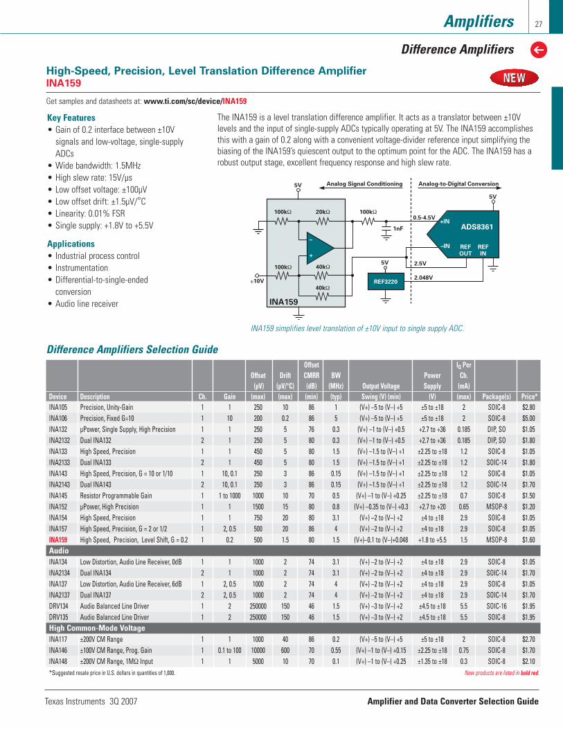
Texas Instruments 3Q 2007 Amplifier and Data Converter Selection Guide
Amplifiers
Difference Amplifiers
27
High-Speed, Precision, Level Translation Difference AmplifierINA159
Get samples and datasheets at: www.ti.com/sc/device/INA159
Key Features• Gain of 0.2 interface between ±10V
signals and low-voltage, single-supplyADCs
• Wide bandwidth: 1.5MHz• High slew rate: 15V/µs• Low offset voltage: ±100µV• Low offset drift: ±1.5µV/°C• Linearity: 0.01% FSR• Single supply: +1.8V to +5.5V
Applications• Industrial process control• Instrumentation• Differential-to-single-ended
conversion• Audio line receiver
The INA159 is a level translation difference amplifier. It acts as a translator between ±10V levels and the input of single-supply ADCs typically operating at 5V. The INA159 accomplishesthis with a gain of 0.2 along with a convenient voltage-divider reference input simplifying thebiasing of the INA159’s quiescent output to the optimum point for the ADC. The INA159 has arobust output stage, excellent frequency response and high slew rate.
+
–
5V
5V
5V
100kΩ 20kΩ 100kΩ
±10V
100kΩ 40kΩ
40kΩ
1nF
0.5-4.5V
Analog Signal Conditioning Analog-to-Digital Conversion
2.5V
2.048V
+IN
REFIN
REFOUT
–IN
ADS8361
REF3220
INA159
INA159 simplifies level translation of ±10V input to single supply ADC.
Difference Amplifiers Selection GuideOffset IQ Per
Offset Drift CMRR BW Power Ch.(µV) (µV/°C) (dB) (MHz) Output Voltage Supply (mA)
Device Description Ch. Gain (max) (max) (min) (typ) Swing (V) (min) (V) (max) Package(s) Price* INA105 Precision, Unity-Gain 1 1 250 10 86 1 (V+) –5 to (V–) +5 ±5 to ±18 2 SOIC-8 $2.80 INA106 Precision, Fixed G=10 1 10 200 0.2 86 5 (V+) –5 to (V–) +5 ±5 to ±18 2 SOIC-8 $5.00 INA132 µPower, Single Supply, High Precision 1 1 250 5 76 0.3 (V+) –1 to (V–) +0.5 +2.7 to +36 0.185 DIP, SO $1.05 INA2132 Dual INA132 2 1 250 5 80 0.3 (V+) –1 to (V–) +0.5 +2.7 to +36 0.185 DIP, SO $1.80 INA133 High Speed, Precision 1 1 450 5 80 1.5 (V+) –1.5 to (V–) +1 ±2.25 to ±18 1.2 SOIC-8 $1.05 INA2133 Dual INA133 2 1 450 5 80 1.5 (V+) –1.5 to (V–) +1 ±2.25 to ±18 1.2 SOIC-14 $1.80 INA143 High Speed, Precision, G = 10 or 1/10 1 10, 0.1 250 3 86 0.15 (V+) –1.5 to (V–) +1 ±2.25 to ±18 1.2 SOIC-8 $1.05 INA2143 Dual INA143 2 10, 0.1 250 3 86 0.15 (V+) –1.5 to (V–) +1 ±2.25 to ±18 1.2 SOIC-14 $1.70 INA145 Resistor Programmable Gain 1 1 to 1000 1000 10 70 0.5 (V+) –1 to (V–) +0.25 ±2.25 to ±18 0.7 SOIC-8 $1.50 INA152 µPower, High Precision 1 1 1500 15 80 0.8 (V+) –0.35 to (V–) +0.3 +2.7 to +20 0.65 MSOP-8 $1.20 INA154 High Speed, Precision 1 1 750 20 80 3.1 (V+) –2 to (V–) +2 ±4 to ±18 2.9 SOIC-8 $1.05 INA157 High Speed, Precision, G = 2 or 1/2 1 2, 0.5 500 20 86 4 (V+) –2 to (V–) +2 ±4 to ±18 2.9 SOIC-8 $1.05 INA159 High Speed, Precision, Level Shift, G = 0.2 1 0.2 500 1.5 80 1.5 (V+)–0.1 to (V–)+0.048 +1.8 to +5.5 1.5 MSOP-8 $1.60 AudioINA134 Low Distortion, Audio Line Receiver, 0dB 1 1 1000 2 74 3.1 (V+) –2 to (V–) +2 ±4 to ±18 2.9 SOIC-8 $1.05 INA2134 Dual INA134 2 1 1000 2 74 3.1 (V+) –2 to (V–) +2 ±4 to ±18 2.9 SOIC-14 $1.70 INA137 Low Distortion, Audio Line Receiver, 6dB 1 2, 0.5 1000 2 74 4 (V+) –2 to (V–) +2 ±4 to ±18 2.9 SOIC-8 $1.05 INA2137 Dual INA137 2 2, 0.5 1000 2 74 4 (V+) –2 to (V–) +2 ±4 to ±18 2.9 SOIC-14 $1.70 DRV134 Audio Balanced Line Driver 1 2 250000 150 46 1.5 (V+) –3 to (V–) +2 ±4.5 to ±18 5.5 SOIC-16 $1.95 DRV135 Audio Balanced Line Driver 1 2 250000 150 46 1.5 (V+) –3 to (V–) +2 ±4.5 to ±18 5.5 SOIC-8 $1.95 High Common-Mode VoltageINA117 ±200V CM Range 1 1 1000 40 86 0.2 (V+) –5 to (V–) +5 ±5 to ±18 2 SOIC-8 $2.70 INA146 ±100V CM Range, Prog. Gain 1 0.1 to 100 10000 600 70 0.55 (V+) –1 to (V–) +0.15 ±2.25 to ±18 0.75 SOIC-8 $1.70 INA148 ±200V CM Range, 1MΩ Input 1 1 5000 10 70 0.1 (V+) –1 to (V–) +0.25 ±1.35 to ±18 0.3 SOIC-8 $2.10 *Suggested resale price in U.S. dollars in quantities of 1,000. New products are listed in bold red.
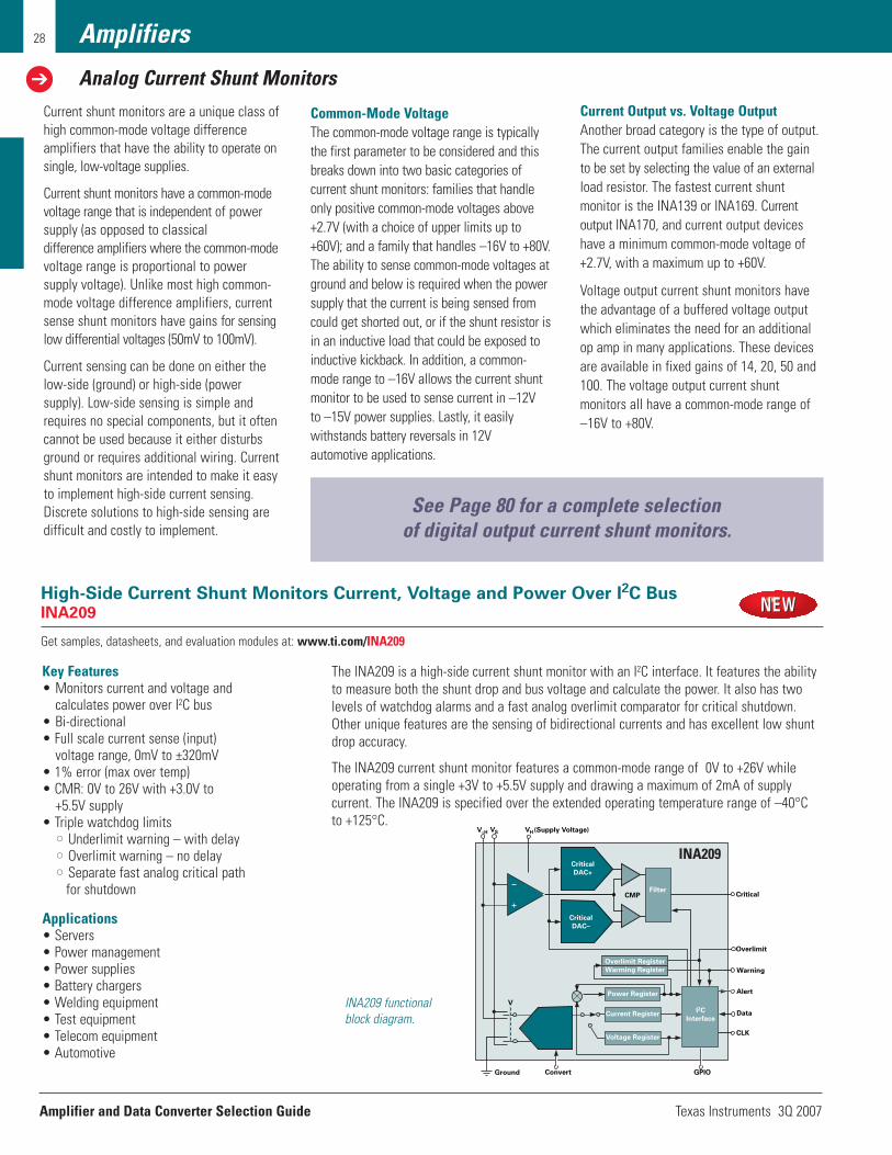
Amplifier and Data Converter Selection Guide Texas Instruments 3Q 2007
28 Amplifiers
Analog Current Shunt Monitors
Current shunt monitors are a unique class ofhigh common-mode voltage difference amplifiers that have the ability to operate onsingle, low-voltage supplies.
Current shunt monitors have a common-modevoltage range that is independent of powersupply (as opposed to classical difference amplifiers where the common-modevoltage range is proportional to power supply voltage). Unlike most high common-mode voltage difference amplifiers, currentsense shunt monitors have gains for sensinglow differential voltages (50mV to 100mV).
Current sensing can be done on either thelow-side (ground) or high-side (power supply). Low-side sensing is simple andrequires no special components, but it oftencannot be used because it either disturbsground or requires additional wiring. Currentshunt monitors are intended to make it easyto implement high-side current sensing.Discrete solutions to high-side sensing aredifficult and costly to implement.
Common-Mode VoltageThe common-mode voltage range is typicallythe first parameter to be considered and thisbreaks down into two basic categories of current shunt monitors: families that handleonly positive common-mode voltages above+2.7V (with a choice of upper limits up to+60V); and a family that handles –16V to +80V.The ability to sense common-mode voltages atground and below is required when the powersupply that the current is being sensed fromcould get shorted out, or if the shunt resistor isin an inductive load that could be exposed toinductive kickback. In addition, a common-mode range to –16V allows the current shuntmonitor to be used to sense current in –12V to –15V power supplies. Lastly, it easily withstands battery reversals in 12V automotive applications.
Current Output vs. Voltage OutputAnother broad category is the type of output.The current output families enable the gainto be set by selecting the value of an externalload resistor. The fastest current shunt monitor is the INA139 or INA169. Current output INA170, and current output deviceshave a minimum common-mode voltage of+2.7V, with a maximum up to +60V.
Voltage output current shunt monitors havethe advantage of a buffered voltage outputwhich eliminates the need for an additionalop amp in many applications. These devicesare available in fixed gains of 14, 20, 50 and100. The voltage output current shunt monitors all have a common-mode range of–16V to +80V.
V–H VS VH (Supply Voltage)
Critical
DAC+
Critical
DAC–
CMPFilter
Critical
Overlimit
Warning
Alert
Data
CLK
GPIO
I2C
Interface
Overlimit Register
Warming Register
Power Register
Current Register
Voltage Register
ConvertGround
V
High-Side Current Shunt Monitors Current, Voltage and Power Over I2C BusINA209
Get samples, datasheets, and evaluation modules at: www.ti.com/INA209
INA209 functional block diagram.
Key Features• Monitors current and voltage and
calculates power over I2C bus• Bi-directional• Full scale current sense (input)
voltage range, 0mV to ±320mV• 1% error (max over temp)• CMR: 0V to 26V with +3.0V to
+5.5V supply• Triple watchdog limits
•• Underlimit warning – with delay•• Overlimit warning – no delay•• Separate fast analog critical path
for shutdown
Applications• Servers• Power management• Power supplies• Battery chargers• Welding equipment• Test equipment• Telecom equipment• Automotive
The INA209 is a high-side current shunt monitor with an I2C interface. It features the abilityto measure both the shunt drop and bus voltage and calculate the power. It also has twolevels of watchdog alarms and a fast analog overlimit comparator for critical shutdown.Other unique features are the sensing of bidirectional currents and has excellent low shuntdrop accuracy.
The INA209 current shunt monitor features a common-mode range of 0V to +26V whileoperating from a single +3V to +5.5V supply and drawing a maximum of 2mA of supply current. The INA209 is specified over the extended operating temperature range of –40°C to +125°C.
See Page 80 for a complete selection of digital output current shunt monitors.
INA209

Texas Instruments 3Q 2007 Amplifier and Data Converter Selection Guide
Amplifiers
Analog Current Shunt Monitors
29
C2IN
VOUT
C1OUT
C2OUT
VREF OUT
RESET
DELAY
V+
C1IN
1.2V Reference
x20
INA206
–16V to +80V, High-Side Current Shunt Monitors with Integrated Dual ComparatorsINA203, INA204, INA205, INA206, INA207, INA208
Get samples, datasheets, and evaluation modules at: www.ti.com/sc/device/PARTnumber (Replace PARTnumber with INA203, INA204, INA205, INA206, INA207 or INA208)
INA206/INA207/INA208 functional block diagram.
Key Features• Extended common mode input range:
–16V to +80V• Integrated dual open-drain
comparators• 1.2V reference• Low offset: 2mV• Rail-to-rail output voltage • Single supply: 2.7V to 18V• Packaging: MSOP, SO-14, TSSOP
Applications• Notebook computers• Cell phones• Telecom equipment• Power management• Battery chargers
The INA203/04/05/06/07/08 feature dual comparators and 1.2V reference. These devices areideal for multilevel watchdog systems, window comparators, or battery detection. Convenientdefault trip points are provided at each comparator of 0.6V. The 14-pin version allows externaloveride of trip points + programmable delay on 2nd comparator. Comparator #1 has a latching capability.
The current shunt amplifiers of the INA203/04/05/06/07/08 feature a common-mode range of–16V to +80V independent of supply voltage, and are powered by single-supply voltages from+2.7V to +18V. The INA20x provides a fully buffered voltage output available in three gains: INA203/INA206 = 20V/V; INA204/INA207 = 50V/V; INA205/INA208 = 100V/V.
Current Shunt Monitors Selection GuideOffset IQ Per
Offset Drift CMRR BW Power Ch.(µV) (µV/ºC) (dB) (MHz) Output Voltage Supply (mA)
Device Description Ch. Gain (max) (max) (typ) (typ) Swing (V) (min) (V) (max) Package(s) Price*
Voltage-Output, High-Side Current Shunt MonitorsINA19x –16V to +80V CMV 1 20, 50, 100V/V 2000 2.5 120 0.5, 0.3, 0.2 V(+) –0.2 +2.7 to 18 0.9 SOT23-5 $0.80 INA20x Single/Dual Comparator, VREF 1 20, 50, 100V/V 2500 5 100 0.5, 0.3, 0.2 V(+) –0.25 +2.7 to 18 2.2 SO-14/TSSOP-14, MSOP-10, $1.25
MSOP/SO/DFN-8INA27x –16V to +18V CMV, Filtering Provision 1 14, 20V/V 2000 2.5 120 0.13 V(+) –0.2 +2.7 to 18 0.9 SO8 $1.25 Current-Output, High-Side Current Shunt MonitorsINA138 36V (max) 1 1 to 100 1000 1 120 0.8 0 to (V+) –0.8 +2.7 to 36 0.045 SOT23-5 $0.95 INA168 60V (max) 1 1 to 100 1000 1 120 0.8 0 to (V+) –0.8 +2.7 to 60 0.045 SOT23-5 $1.25 INA139 High Speed, 40V (max) 1 1 to 100 1000 1 115 0.44 0 to (V+) –1.2 +2.7 to 40 0.125 SOT23-5 $0.99 INA169 High Speed, 60V (max) 1 1 to 100 1000 1 120 0.44 0 to (V+) –1.2 +2.7 to 60 0.125 SOT23-5 $1.25 Bidirectional Current Shunt MonitorsINA170 60V (max) 1 1 to 100 1000 1 120 0.4 0 to V(+) –1.2 +2.7 to 40 0.125 MSOP-8 $1.25INA209 Voltage Current, Power Over I2C 1 — 100 10 120 34 — 3.5V to 5.5V 2 TSSOP-16 $3.50
*Suggested resale price in U.S. dollars in quantities of 1,000. New products are listed in bold red.
INA206
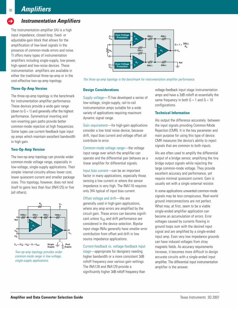
Amplifier and Data Converter Selection Guide Texas Instruments 3Q 2007
30 Amplifiers
Instrumentation Amplifiers
The instrumentation amplifier (IA) is a highinput impedance, closed-loop, fixed- oradjustable-gain block that allows for theamplification of low-level signals in the presence of common-mode errors and noise.TI offers many types of instrumentationamplifiers including single-supply, low-power,high-speed and low-noise devices. Theseinstrumentation amplifiers are available ineither the traditional three-op-amp or in the cost-effective two-op-amp topology.
Three-Op-Amp Version
The three-op-amp topology is the benchmarkfor instrumentation amplifier performance.These devices provide a wide gain range(down to G = 1) and generally offer the highestperformance. Symmetrical inverting and non-inverting gain paths provide better common-mode rejection at high frequencies.Some types use current-feedback-type inputop amps which maintain excellent bandwidthin high gain.
Two-Op-Amp Version
The two-op-amp topology can provide widercommon-mode voltage range, especially inlow-voltage, single-supply applications. Theirsimpler internal circuitry allows lower cost,lower quiescent current and smaller packagesizes. This topology, however, does not lenditself to gains less than four (INA125) or five(all others).
Design Considerations
Supply voltage—TI has developed a series oflow-voltage, single-supply, rail-to-rail instrumentation amps suitable for a widevariety of applications requiring maximumdynamic signal range.
Gain requirement—for high-gain applicationsconsider a low total noise device, becausedrift, input bias current and voltage offset allcontribute to error.
Common-mode voltage range—the voltageinput range over which the amplifier canoperate and the differential pair behaves as alinear amplifier for differential signals.
Input bias current—can be an important factor in many applications, especially thosesensing a low current or where the sensorimpedance is very high. The INA116 requiresonly 3fA typical of input bias current.
Offset voltage and drift—IAs are generally used in high-gain applications,where any amp errors are amplified by thecircuit gain. These errors can become signifi-cant unless VOS and drift performance areconsidered in the device selection. Bipolarinput stage INAs generally have smaller errorcontribution from offset and drift in lowsource impedance applications.
Current-feedback vs. voltage-feedback inputstage—appropriate for designers needinghigher bandwidth or a more consistent 3dBrolloff frequency over various gain settings.The INA128 and INA129 provide a significantly higher 3dB rolloff frequency than
voltage-feedback input stage instrumentationamps and have a 3dB rolloff at essentially thesame frequency in both G = 1 and G = 10 configurations.
Technical Information
IAs output the difference accurately betweenthe input signals providing Common-ModeRejection (CMR). It is the key parameter andmain purpose for using this type of device.CMR measures the device’s ability to rejectsignals that are common to both inputs.
IAs are often used to amplify the differentialoutput of a bridge sensor, amplifying the tinybridge output signals while rejecting thelarge common-mode voltage. They provideexcellent accuracy and performance, yetrequire minimal quiescent current. Gain isusually set with a single external resistor.
In some applications unwanted common-modesignals may be less conspicuous. Real-worldground interconnections are not perfect.What may, at first, seem to be a viable single-ended amplifier application canbecome an accumulation of errors. Error voltages caused by currents flowing inground loops sum with the desired input signal and are amplified by a single-endedinput amp. Even very low impedance groundscan have induced voltages from stray magnetic fields. As accuracy requirementsincrease, it becomes more difficult to designaccurate circuits with a single-ended inputamplifier. The differential input instrumentationamplifier is the answer.
25kΩ 100kΩ
Ref
VO
25kΩ100kΩ
V+RG
Single Supply
Dual Supply
V–
A1
A2VIN
VIN
VO = (VIN – VIN) • G + VREF
25kΩ
60kΩ 60kΩ
60kΩ60kΩ
50kΩG = 1 +
RG
VO
Ref
RGA3
A1
A2
VIN
VIN
Over-VoltageProtection
Over-VoltageProtection
The three-op-amp topology is the benchmark for instrumentation amplifier performance.
Two-op-amp topology provides wider common-mode range in low-voltage, single-supply applications.
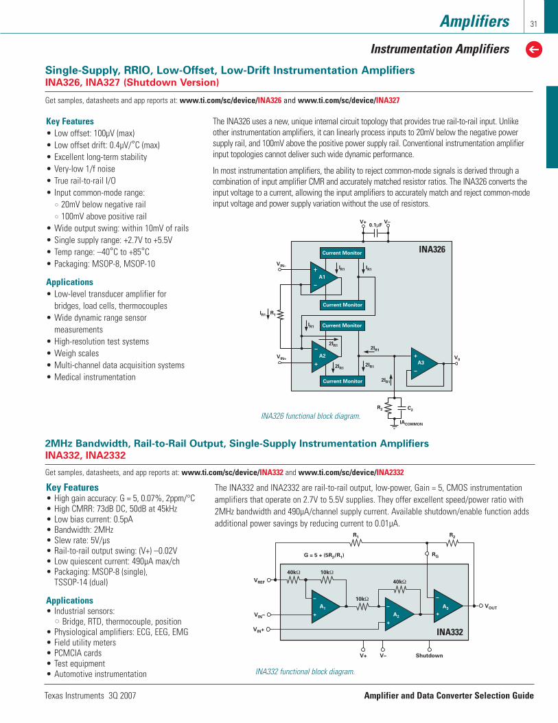
Texas Instruments 3Q 2007 Amplifier and Data Converter Selection Guide
Amplifiers
Instrumentation Amplifiers
31
Single-Supply, RRIO, Low-Offset, Low-Drift Instrumentation AmplifiersINA326, INA327 (Shutdown Version)
Get samples, datasheets and app reports at: www.ti.com/sc/device/INA326 and www.ti.com/sc/device/INA327
Key Features• Low offset: 100µV (max)• Low offset drift: 0.4µV/°C (max)• Excellent long-term stability• Very-low 1/f noise• True rail-to-rail I/O• Input common-mode range:
•• 20mV below negative rail •• 100mV above positive rail
• Wide output swing: within 10mV of rails• Single supply range: +2.7V to +5.5V• Temp range: –40°C to +85°C• Packaging: MSOP-8, MSOP-10
Applications• Low-level transducer amplifier for
bridges, load cells, thermocouples• Wide dynamic range sensor
measurements• High-resolution test systems• Weigh scales• Multi-channel data acquisition systems• Medical instrumentation
The INA326 uses a new, unique internal circuit topology that provides true rail-to-rail input. Unlikeother instrumentation amplifiers, it can linearly process inputs to 20mV below the negative powersupply rail, and 100mV above the positive power supply rail. Conventional instrumentation amplifierinput topologies cannot deliver such wide dynamic performance.
In most instrumentation amplifiers, the ability to reject common-mode signals is derived through acombination of input amplifier CMR and accurately matched resistor ratios. The INA326 converts theinput voltage to a current, allowing the input amplifiers to accurately match and reject common-modeinput voltage and power supply variation without the use of resistors.
V+ V–0.1µF
Current Monitor
IR1
VIN– IR1
Current Monitor
IR1 R1
IR1 Current Monitor
2IR1
VIN+
Current Monitor
2IR12IR1
2IR1
A3
R2 C2
IACOMMON
2IR1
V0
A1
A2
INA326 functional block diagram.
A2
A1 A3
40kΩ
VREF
VIN–
VIN+
10kΩ
10kΩ
ShutdownV+
VOUT
G = 5 + (5R2/R1)
V–
R2R1
RG
40kΩ
–
+
–
+
–
+
2MHz Bandwidth, Rail-to-Rail Output, Single-Supply Instrumentation Amplifiers
INA332, INA2332
Get samples, datasheets, and app reports at: www.ti.com/sc/device/INA332 and www.ti.com/sc/device/INA2332
INA332 functional block diagram.
Key Features• High gain accuracy: G = 5, 0.07%, 2ppm/°C• High CMRR: 73dB DC, 50dB at 45kHz• Low bias current: 0.5pA• Bandwidth: 2MHz• Slew rate: 5V/µs• Rail-to-rail output swing: (V+) –0.02V• Low quiescent current: 490µA max/ch• Packaging: MSOP-8 (single),
TSSOP-14 (dual)
Applications• Industrial sensors:
•• Bridge, RTD, thermocouple, position• Physiological amplifiers: ECG, EEG, EMG• Field utility meters• PCMCIA cards• Test equipment• Automotive instrumentation
The INA332 and INA2332 are rail-to-rail output, low-power, Gain = 5, CMOS instrumentationamplifiers that operate on 2.7V to 5.5V supplies. They offer excellent speed/power ratio with2MHz bandwidth and 490µA/channel supply current. Available shutdown/enable function addsadditional power savings by reducing current to 0.01µA.
INA326
INA332
Amplifier and Data Converter Selection Guide Texas Instruments 3Q 2007
Amplifiers
Single-Supply Instrumentation Amplifiers
32
Single-Supply Instrumentation Amplifiers Selection GuideInput Offset CMRR BW IQ
Non Bias at Offset at at Noise PerLinearity Current G = 100 Drift G = 100 G = 100 1kHz Power Amp
(%) (nA) (µV) (µV/°C) (dB) (kHz) (nV/ Hz) Supply (mA)Device Description Gain (max) (max) (max) (max) (min) (min) (typ) (V) (max) Package(s) Price*
Single-Supply, Low-Power, IQ < 525µA per Instrumentation AmpINA321 RRO, SHDN, Low Offset, Gain Error, Wide Temp 5 to1000 0.01 0.01 1000 71 90 50 100 2.7 to 5.5 0.06 MSOP-8 $1.10 INA2321 Dual INA321 5 to1000 0.01 0.01 1000 71 90 50 100 2.7 to 5.5 0.06 TSSOP-14 $1.75 INA322 RRO, SHDN, Wide Temp, Low Cost 5 to 1000 0.01 0.01 10000 7 60 50 100 2.7 to 5.5 0.06 MSOP-8 $0.95 INA2322 Dual INA322 5 to 1000 0.01 0.01 10000 7 60 50 100 2.7 to 5.5 0.06 TSSOP-14 $1.50 INA122 µPower, RRO, CM to GND 5 to 10000 0.012 25 250 3 90 5 60 2.2 to 36 0.085 DIP-8, SOIC-8 $2.10 INA332 RRO, Wide BW, SHDN, Wide Temp, Low Cost 5 to 1000 0.01 0.01 10000 71 60 500 100 2.7 to 5.5 0.1 MSOP-8 $0.85 INA2332 Dual INA332 5 to 1000 0.01 0.01 10000 71 60 500 100 2.7 to 5.5 0.1 MSOP-8 $1.35 INA126 µPower, < 1V VSAT, Low Cost 5 to 10000 0.012 25 250 3 83 9 35 2.7 to 36 0.2 DIP/SO/MSOP-8 $1.05 INA2126 Dual INA126 5 to 10000 0.012 25 250 3 83 9 35 2.7 to 36 0.2 DIP/SO/MSOP-16 $1.70 INA118 Precision, Low Drift, Low Power2 1 to 10000 0.002 5 55 0.7 107 70 10 2.7 to 36 0.385 DIP-8, SOIC-8 $4.15 INA331 RRO, Wide BW, SHDN, Wide Temp 5 to 1000 0.01 0.01 500 51 90 2000 46 2.7 to 5.5 0.5 MSOP-8 $1.10 INA2331 Dual INA331 5 to 1000 0.01 0.01 1000 51 80 2000 46 2.7 to 5.5 0.5 TSSOP-14 $1.80 INA125 Internal Ref, Sleep Mode2 4 to 10000 0.01 25 250 2 100 4.5 38 2.7 to 36 0.525 DIP-8, SOIC-16 $2.05 Single-Supply, Low Input Bias Current, IB < 50pAINA155 Low Offset, RRO, Wide Temp, SR = 6.5V/µs 10, 50 0.015 0.01 1000 51 86 110 40 2.7 to 5.5 2.1 MSOP-8 $1.10 INA156 Low Offset, RRO, Low Cost, Wide Temp, SR = 6.5V/µs 10, 50 0.015 0.01 8000 51 86 110 40 2.7 to 5.5 2.1 SOIC-8, $0.95 INA321 RRO, SHDN, Low Offset, Gain Error, Wide Temp 5 to 1000 0.01 0.01 1000 71 90 50 100 2.7 to 5.5 0.06 MSOP-8 $1.10 INA2321 Dual INA321 5 to 1000 0.01 0.01 1000 71 90 50 100 2.7 to 5.5 0.06 TSSOP-14 $1.75 INA322 RRO, SHDN, Wide Temp, Low Cost 5 to 1000 0.01 0.01 10000 7 60 50 100 2.7 to 5.5 0.06 MSOP-8 $0.95 INA2322 Dual INA322 5 to 1000 0.01 0.01 10000 7 60 50 100 2.7 to 5.5 0.06 TSSOP-14 $1.50 INA331 RRO, Wide BW, SHDN, Wide Temp 5 to 1000 0.01 0.01 500 51 90 2000 46 2.7 to 5.5 0.5 MSOP-8 $1.10 INA2331 Dual INA331 5 to 1000 0.01 0.01 1000 51 80 2000 46 2.7 to 5.5 0.5 TSSOP-14 $1.80 INA332 RRO, Wide BW, SHDN, Wide Temp, Low Cost 5 to 1000 0.01 0.01 10000 71 60 500 100 2.7 to 5.5 0.1 MSOP-8 $0.85 INA2332 Dual INA332 5 to 1000 0.01 0.01 10000 71 60 500 100 2.7 to 5.5 0.1 TSSOP-14 $1.35 Single-Supply, Precision, VOS < 300µV, Low VOS DriftINA118 Precision, Low Drift, Low Power2 1 to 10000 0.002 5 55 0.7 107 70 10 2.7 to 36 0.385 DIP-8, SOIC-8 $4.15 INA326 RRIO, Auto- Zero, CM > Supply, Low Drift 0.1 to 10000 0.01 2 100 0.4 100 1 33 2.7 to 5.5 3.4 MSOP-8 $1.80 INA327 RRIO, Auto-Zero, SHDN, CM > Supply, Low Drift 0.1 to 10000 0.01 2 100 0.4 100 1 33 2.7 to 5.5 3.4 MSOP-10 $1.95 INA337 RRIO, Auto-Zero, Low Drift, CM > Supply, 0.1 to 10000 0.01 2 100 0.4 106 1 33 2.7 to 5.5 3.4 MSOP-8 $1.80
Wide Temp INA338 RRIO, Auto-Zero, Low Drift, CM > Supply, 0.1 to 10000 0.01 2 100 0.4 106 1 33 2.7 to 5.5 3.4 MSOP-10 $1.95
SHDN, Wide Temp INA122 µPower, RRO, CM to GND 5 to 10000 0.012 25 250 3 90 5 60 2.2 to 36 0.085 DIP-8, SOIC-8 $2.10 INA125 Internal Ref, Sleep Mode2 4 to 10000 0.01 25 250 2 100 4.5 38 2.7 to 36 0.525 DIP-8, SOIC-16 $2.05 INA126 µPower, < 1V VSAT, Low Cost 5 to 10000 0.012 25 250 3 83 9 35 2.7 to 36 0.2 DIP/SO/MSOP-8 $1.05 INA2126 Dual INA126 5 to 10000 0.012 25 250 3 83 9 35 2.7 to 36 0.2 DIP/SO/MSOP-16 $1.70 Signal Amplifiers for Temperature Control IB (nA) Temp Error3 1⁄F NoiseINA330 Optimized for Precision 10kΩ — — 0.23 — 0.009°C1 — 1 0.0001°C pp1 2.7 to 5.5 3.6 MSOP-10 $1.55
Thermistor Applications 1 Typical 2 Internal +40V input protection 3 –40°C to +85°C*Suggested resale price in U.S. dollars in quantities of 1,000.

Texas Instruments 3Q 2007 Amplifier and Data Converter Selection Guide
Amplifiers
Dual-Supply Instrumentation Amplifiers
33
Dual-Supply Instrumentation Amplifiers Selection GuideInput Offset CMRR BW IQ
Non Bias at Offset at at Noise PerLinearity Current G = 100 Drift G = 100 G = 100 1kHz Power Amp
(%) (nA) (µV) (µV/°C) (dB) (kHz) (nV/√ Hz) Supply (mA)Device Description Gain (max) (max) (max) (max) (min) (min) (typ) (V) (max) Package(s) Price*Dual-Supply, Low-Power, IQ < 850µA per Instrumentation AmpINA122 µPower, RRO, CM to GND 5 to 10000 0.012 25 250 3 90 5 60 ±1.3 to ±18 0.085 DIP-8, SOIC-8 $2.10 INA1262 µPower, < 1V VSAT, Low Cost 5 to 10000 0.012 25 250 3 83 9 35 ±1.35 to ±18 0.2 DIP/SO/MSOP-8 $1.05 INA118 Precision, Low Drift, Low Power1 1 to 10000 0.002 5 55 0.7 107 70 10 ±1.35 to ±18 0.385 DIP-8, SOIC-8 $4.15 INA121 Low Bias, Precision, Low Power1 1 to 10000 0.005 0.05 500 5 100 50 20 ±2.25 to ±18 0.525 DIP-8, SO-8 $2.50 INA125 Internal Ref, Sleep Mode1 4 to 10000 0.01 25 250 2 100 4.5 38 ±1.35 to ±18 0.525 DIP-8, SOIC-16 $2.05 INA1282 Precision, Low Noise, Low Drift1 1 to 10000 0.002 5 60 0.7 120 200 8 ±2.25 to ±18 0.8 DIP-8, SOIC-8 $3.05 INA129 Precision, Low Noise, Low Drift,1 1 to 10000 0.002 5 60 0.7 120 200 8 ±2.25 to +18 0.8 DIP-8, SOIC-8 $3.05
AD620 Second Source INA1412 Precision, Low Noise, Low Power, 10, 100 0.002 5 50 0.5 110 200 8 ±2.25 to +18 0.8 DIP-8, SOIC-8 $3.55
Pin Compatible with AD62121 Dual-Supply, Low Input Bias Current, IB < 50pAINA110 Fast Settle, Low Noise, Wide BW 1, 10, 100, 0.01 0.05 280 2.5 106 470 10 ±6 to ±18 4.5 DIP-16, SOIC-16 $7.00
200, 500 INA121 Precision, Low Power1 1 to 10000 0.005 0.05 500 5 100 50 20 ±2.25 to ±18 0.525 DIP-8, SO-8 $2.50 INA111 Fast Settle, Low Noise, Wide BW 1 to 1000 0.005 0.02 520 6 106 450 10 ±6 to ±18 4.5 DIP-8, SO-16 $4.20 INA116 Ultra Low IB 3fA (typ), with Buffered 1 to 1000 0.01 0.0001 5000 40 80 70 28 ±4.5 to ±18 1.4 DIP-16, SO-16 $4.20
Guard Drive Pins1
Dual-Supply, Precision VOS < 300µV, Low VOS DriftINA114 Precision, Low Drift1 1 to 10000 0.002 2 50 0.25 110 10 11 ±2.25 to ±18 3 DIP-8, SO-16 $4.20 INA115 Precision, Low Drift, w/Gain Sense Pins1 1 to 10000 0.002 2 50 0.25 120 10 11 ±2.25 to ±18 3 SO-16 $4.20 INA131 Low Noise, Low Drift1 100 0.002 2 50 0.25 110 70 12 ±2.25 to ±18 3 DIP-8 $3.80 INA1412 Precision, Low Noise, Low Power, 10, 100 0.002 5 50 0.5 110 200 8 ±2.25 to ±18 0.8 DIP-8, SOIC-8 $3.55
Pin Compatible with AD62121 INA118 Precision, Low Drift, Low Power1 1 to 10000 0.002 5 55 0.7 107 70 10 ±1.35 to ±18 0.385 DIP-8, SOIC-8 $4.15 INA1282 Precision, Low Noise, Low Drift1 1 to 10000 0.002 5 60 0.7 120 200 8 ±2.25 to ±18 0.8 DIP-8, SOIC-8 $3.05 INA129 Precision, Low Noise, Low Drift, 1 to 10000 0.002 5 60 0.7 120 200 8 ±2.25 to ±18 0.8 DIP-8, SOIC-8 $3.05
AD620 Second Source1
INA122 µPower, RRO, CM to GND 5 to 10000 0.012 25 250 3 90 5 60 ±1.3 to ±18 0.085 DIP-8, SOIC-8 $2.10 INA125 Internal Ref, Sleep Mode1 4 to 10000 0.01 25 250 2 100 4.5 38 ±1.35 to ±18 0.525 DIP-8, SOIC-16 $2.05 INA1262 µPower, < 1V VSAT, Low Cost 5 to 10000 0.012 25 250 3 83 9 35 ±1.35 to ±18 0.2 DIP/SO/MSOP-8 $1.05 INA101 Low Noise, Wide BW, Gain Sense Pins, 1 to 1000 0.002 30 250 0.25 100 25 13 ±5 to ±20 8.5 PDIP-14, SO-16 $7.95
Wide Temp INA110 Fast Settle, Low Noise, Low Bias, Wide BW 1, 10, 100, 0.01 0.05 280 2.5 106 470 10 ±6 to ±18 4.5 CDIP-16 $7.00
200, 500 Dual-Supply, Lowest NoiseINA103 Precision, Fast Settle, Low Drift, Audio, 1, 100 0.00063 12000 255 1.23 100 800 1 ±9 to ±25 13 DIP-16, SO-16 $5.00
Mic Pre Amp, THD+N = 0.0009% INA163 Precision, Fast Settle, Low Drift, Audio, 1 to 10000 0.00063 12000 300 1.23 100 800 1 ±4.5 to ±18 12 SOIC-14 $2.50
Mic Pre Amp, THD+N = 0.002% INA166 Precision, Fast Settle, Low Drift, Audio, 2000 0.005 12000 300 2.53 100 450 1.3 ±4.5 to ±18 12 SO-14 Narrow $5.95
Mic Pre Amp, THD+N = 0.09% INA217 Precision, Low Drift, Audio, Mic PreAmp, 1 to 10000 0.00063 12000 300 1.23 100 800 1.3 ±4.5 to ±18 12 DIP-8, SO-16 $2.50
THD+N = 0.09%, SSM2017 Replacement 1 Internal +40V input protection.2 Parts also available in dual version.*Suggested resale price in U.S. dollars in quantities of 1,000.

Amplifier and Data Converter Selection Guide Texas Instruments 3Q 2007
34 Amplifiers
Programmable Gain Amplifiers
Programmable gain instrumentationamplifiers (PGAs) are extremely versatiledata acquisition input amplifiers that provide digital control of gain forimproved accuracy and extended dynamicrange. Many have inputs that are protectedto ±40V even with the power supply off.A single input amplifier type can be connected to a variety of sensors or signals. Under processor control, theswitched gain extends the dynamic rangeof the system.
All PGA-series amps have TTL- or CMOS-compatible inputs for easy microprocessorinterface. Inputs are laser trimmed forlow offset voltage and low drift to allowuse without the need of external components.
Design ConsiderationsPrimary
Digitally-selected gain required—twopins allow the selection of up to four different gain states. A PGA202 andPGA203 can be put in series for greatergain selection.
Non-linearity (accuracy)—depends heavilyon what is being driven. A 16-bit converterwill require significantly better accuracy(i.e., lower non-linearity) than a 10-bitconverter.
Secondary
Gain error and drift—for higher gain,high-precision applications will requirecloser attention to drift and gain error.
Input bias current— high source impedanceapplications often require FET-input ampsto minimize bias current errors.
Technical Information
The PGA206 provides binary gain steps of1, 2, 4 and 8V/V, selected by CMOS- orTTL-compatible inputs. The PGA207 hasgains of 1, 2, 5 and 10V/V, adding a fulldecade to the system dynamic range. Thelow input bias current, FET-input stageassures that series resistance of the multiplexer does not introduce errors.Fast settling time (3.5µs to 0.01%) allowsfast polling of many channels.
The PGA204 and PGA205 have precisionbipolar input stages especially well suited to low-level signals. The PGA205has gain steps of 1, 2, 4 and 8.
Typical Applications• Data acquisition• Auto-ranging circuits• Remote instrumentation• Test equipment• Medical/physiological instrumentation• General analog interface boards
GAIN
PGA205 PGA205
1248
163264
A3
0011111
A2
0101111
A1
0000011
A0
0000101
VIN
+
VIN
–
VOAO
A1A1
AO
Connecting two programmable gain amps can provide binary gain steps G = 1 to G = 64.
Digitally Programmable Gain Amplifiers Selection GuideNon CMRR BW Noise
Linearity Offset at at atat Offset Drift G = 100 G = 100 1kHz Power IQ
G = 100 (µV) (µV/°C) (dB) (kHz) (nV/ Hz) Supply (mA)Device Description Gain (%) (max) (max) (max) (min) (typ) (typ) (V) (max) Package(s) Price*
PGA103 Precision, Single-Ended Input 1, 10, 100 0.01 500 2 (typ) — 250 11 ±4.5 to ±18 3.5 SOIC-8 $4.35 PGA202 High Speed, FET-Input, 50pA IB 1, 10, 100, 0.012 1000 12 92 1000 12 ±4.5 to ±18 6.5 DIP-14 $7.75
1000PGA203 High Speed, FET-Input, 50pA IB 1, 2, 4, 8 0.012 1000 12 92 1000 12 ±4.5 to ±18 6.5 DIP-14 $7.75 PGA204 High Precision, Gain Error: 0.25% 1, 10, 100, 0.002 50 0.25 110 10 13 ±4.5 to ±18 6.5 SOIC-16, PDIP-16 $7.25
1000PGA205 Gain Drift: 0.024ppm/°C 1, 2, 4, 8 0.002 50 0.25 95 100 15 ±4.5 to ±18 6.5 SOIC-16, PDIP-16 $7.25 PGA206 High Speed, FET-Input, 100pA IB 1, 2, 4, 8 0.002 1500 2 (typ) 95 600 18 ±4.5 to ±18 13.5 DIP-16, SOIC-16 $10.80 PGA207 High Speed, FET-Input, 100pA IB 1, 2, 5, 10 0.002 1500 2 (typ) 95 600 18 ±4.5 to ±18 13.5 DIP-16, SOIC-16 $11.85 PGA309 0.1% Digitally Calibrated 8 to 11 0.01 3000 5 (typ) 20 60 210 +2.7 to +5.5 1.6 TSSOP-16 $2.95
Bridge Sensor Conditioner,Voltage Output
*Suggested resale price in U.S. dollars in quantities of 1,000.
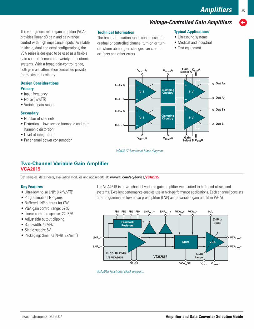
Texas Instruments 3Q 2007 Amplifier and Data Converter Selection Guide
Amplifiers
Voltage-Controlled Gain Amplifiers
35
MUX
52dB
Range
Feedback
Resistors
(3, 12, 18, 22dB)
LNP
+1
1/2 VCA2615
LNPIN+
LNPOUT–FB1 FB2 FB3 FB4
+1
LNPOUT+ VCAIN+ VCAIN– H/L
(0dB or
+6dB)
G1 G2 VCNTL VCLMPVCAINSEL
LNPIN–
VCAOUT+
VCAOUT–
VGA
VCA2615
Two-Channel Variable Gain AmplifierVCA2615
Get samples, datasheets, evaluation modules and app reports at: www.ti.com/sc/device/VCA2615
VCA2615 functional block diagram.
Key Features• Ultra-low noise LNP: 0.7nV/ Hz• Programmable LNP gains• Buffered LNP outputs for CW• VGA gain control range: 52dB• Linear control response: 22dB/V• Adjustable output clipping• Bandwidth: 42MHz• Single supply: 5V• Packaging: Small QFN-48 (7x7mm2)
The VCA2615 is a two-channel variable gain amplifier well suited to high-end ultrasound systems. Excellent performance enables use in high-performance applications. Each channel consistsof a programmable low noise preamplifier (LNP) and a variable gain amplifier (VGA).
The voltage-controlled gain amplifier (VCA)provides linear dB gain and gain-range control with high impedance inputs. Availablein single, dual and octal configurations, theVCA series is designed to be used as a flexible gain-control element in a variety of electronicsystems. With a broad gain-control range,both gain and attenuation control are providedfor maximum flexibility.
Design ConsiderationsPrimary • Input frequency• Noise (nV/ Hz)• Variable gain range
Secondary• Number of channels• Distortion—low second harmonic and third
harmonic distortion• Level of integration• Per channel power consumption
Technical InformationThe broad attenuation range can be used forgradual or controlled channel turn-on or turn-off where abrupt gain changes can createartifacts and other errors.
Typical Applications• Ultrasound systems• Medical and industrial• Test equipment
GainSelect B
Out B–
Out A+
Out A–In A–-
In A+
VCNTLA VCLMPA
VCNTLB VCLMPB
CEXTA
CEXTB
In B –
In B+
GainSelect A
Out B+
V- I I- V
ClampingCircuitryV- I I- V
ClampingCircuitry
VCA2617 functional block diagram.
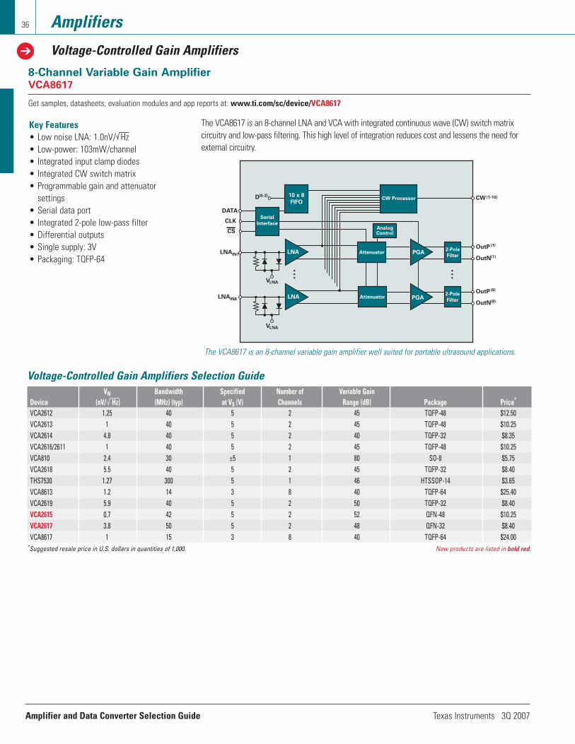
Amplifier and Data Converter Selection Guide Texas Instruments 3Q 2007
Amplifiers
Voltage-Controlled Gain Amplifiers
36
OutP(1)
OutN(1)LNAIN1 LNA
VLNA
VLNA
Attenuator
AnalogControl
PGA2-Pole
Filter
CW(1-10)D(0-3)CW Processor
10 x 8
FIFO
OutP(8)
OutN(8)LNAIN8 LNA Attenuator PGA
•••
•••
DATA
CLK
CS
Serial
Interface
2-Pole
Filter
8-Channel Variable Gain AmplifierVCA8617
Get samples, datasheets, evaluation modules and app reports at: www.ti.com/sc/device/VCA8617
The VCA8617 is an 8-channel variable gain amplifier well suited for portable ultrasound applications.
Key Features• Low noise LNA: 1.0nV/ Hz• Low-power: 103mW/channel• Integrated input clamp diodes• Integrated CW switch matrix• Programmable gain and attenuator
settings• Serial data port• Integrated 2-pole low-pass filter• Differential outputs• Single supply: 3V• Packaging: TQFP-64
The VCA8617 is an 8-channel LNA and VCA with integrated continuous wave (CW) switch matrix circuitry and low-pass filtering. This high level of integration reduces cost and lessens the need forexternal circuitry.
Voltage-Controlled Gain Amplifiers Selection GuideVN Bandwidth Specified Number of Variable Gain
Device (nV/ Hz) (MHz) (typ) at VS (V) Channels Range (dB) Package Price*
VCA2612 1.25 40 5 2 45 TQFP-48 $12.50VCA2613 1 40 5 2 45 TQFP-48 $10.25VCA2614 4.8 40 5 2 40 TQFP-32 $8.35VCA2616/2611 1 40 5 2 45 TQFP-48 $10.25VCA810 2.4 30 ±5 1 80 SO-8 $5.75VCA2618 5.5 40 5 2 45 TQFP-32 $8.40THS7530 1.27 300 5 1 46 HTSSOP-14 $3.65VCA8613 1.2 14 3 8 40 TQFP-64 $25.40VCA2619 5.9 40 5 2 50 TQFP-32 $8.40VCA2615 0.7 42 5 2 52 QFN-48 $10.25VCA2617 3.8 50 5 2 48 QFN-32 $8.40VCA8617 1 15 3 8 40 TQFP-64 $24.00
*Suggested resale price in U.S. dollars in quantities of 1,000. New products are listed in bold red.
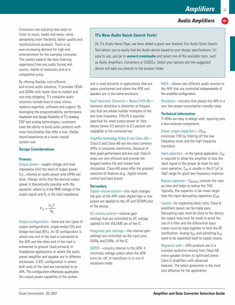
Texas Instruments 3Q 2007 Amplifier and Data Converter Selection Guide
Amplifiers
Audio Amplifiers
37
Consumers are enjoying new ways to listen to music, books and news, whiledemanding more flexibility, better quality andmultifunctional products. There is an ever-increasing demand for high-end entertainment for the everyday consumer.The market expects the best listening experience from any audio format and source, mobile or stationary and at a competitive price.
By offering flexible, cost-efficient, end-to-end audio solutions, TI provides OEMsand ODMs with faster time-to-market andone-stop shopping. TI's complete audio solutions include best-in-class silicon, systems expertise, software and support. Byleveraging the programmability, performanceheadroom and design flexibility of TI's leadingDSP and analog technologies, customershave the ability to build audio products withmore functionality that offer a true, lifelikesound experience at a lower overall system cost.
Design Considerations
PrimaryOutput power—supply voltage and loadimpedance limit the level of output power(i.e., volume) an audio power amp (APA) candrive. Always verify that the desired outputpower is theoretically possible with the equation: where VO is the RMS voltage of theoutput signal and RL is the load impedance.
Output configuration—there are two types ofoutput configurations, single-ended (SE) andbridge-tied load (BTL). An SE configuration iswhere one end of the load is connected tothe APA and the other end of the load is connected to ground. Used primarily in headphone applications or where the audiopower amplifier and speaker are in differentenclosures. A BTL configuration is whereboth ends of the load are connected to anAPA. This configuration effectively quadruplesthe output power capability of the system
and is used primarily in applications that arespace constrained and where the APA andspeaker are in the same enclosure.
Total Harmonic Distortion + Noise (THD+N)—harmonic distortion is distortion at frequen-cies that are whole number multiples of thetest tone frequency. THD+N is typically specified for rated output power at 1kHz.Values below 0.5 percent to 0.3 percent are negligible to the untrained ear.
Amplifier technology (Class-D and Class-AB)—Class-D and Class-AB are the most commonAPAs in consumer electronics, because oftheir great performance and low cost. Class-Damps are very efficient and provide thelongest battery life and lowest heat dissipation. Class-AB amps offer the greatestselection of features (e.g., digital volume control and bass boost).
SecondaryDigital volume control—this input changesthe gain of the APA when digital high or lowpulses are applied to the UP and DOWN pinsof the device.
DC volume control—internal gain settings that are controlled by DC voltageapplied to the VOLUME pin of the IC.
Integrated gain settings—the internal gainsettings are controlled via the input pins,GAIN0 and GAIN1, of the IC.
DEPOP—circuitry internal to the APA. It minimizes voltage spikes when the APA turns on, off, or transitions in or out of shutdown mode.
MUX—allows two different audio sources tothe APA that are controlled independently ofthe amplifier configuration.
Shutdown—circuitry that places the APA in avery low power consumption standby state.
Technical InformationTI APAs are easy to design with, requiring onlya few external components.
Power supply capacitors—CVDDminimizes THD by filtering off the low frequency noise and the high frequency transients.
Input capacitors—in the typical application, CIN,is required to allow the amplifier to bias theinput signal to the proper dc level for opti-mum operation. CIN is usually in the 0.1µF to10µF range for good low-frequency response.
Bypass capacitor—CBYPASS controls the startup time and helps to reduce the THD.Typically, this capacitor is ten times largerthan the input decoupling capacitors (CIN).
Layout—by respecting basic rules, Class-Damplifiers layout can be made easy.Decoupling caps must be close to the device,the output loop must be small to avoid theuse of a filter and the differential input traces must be kept together to limit the RFrectification. Analog VDD and switching VDDneed to be separated back to supply source.
Migration path—APA products are in a constant evolution moving from Class-ABmono speaker drivers to optimized stereoClass-D amplifiers with advanced features. The latest generation is the mostcost effective for the application.
PO =VO2
RL
TI’s New Audio Quick Search Tools!
On TI’s Audio Home Page, we have added a great new feature! Our Audio Quick Search
Tool allows you to easily find the Audio device based on your design specifications. It’s
easy to use, just go to www.ti.com/audio and select one of the available tools, such
as Audio Amplifiers, Converters or CODECs. Select your options and the suggested
device will take you directly to the product folder.
Amplifier and Data Converter Selection Guide Texas Instruments 3Q 2007
Amplifiers
Audio Amplifiers
38
F E A T U R E D P R O D U C T
Key
Multichannel, Pin/SW Compatible
Multichannel
Stereo
• 6 channel• Volume, channel mapping• Bass management• 107-dB dynamic range
TAS5086
• 8 channel• 48-bit audio processing• Volume, channel mapping• PSU volume control• 102-dB dynamic range
TAS5028
• 8 channel• 48-bit audio processing• Volume, EQ, treble/bass, loudness• PSU volume control• 102-dB dynamic range
TAS5508B
• 4 channel• 48-bit audio processing• Volume, EQ, treble/bass, loudness• PSU volume control• 102-dB dynamic range
TAS5504A
• 24 bit, stereo• 94-/96-/102-dB dynamic range• 32- to 192-kHz
TAS5001/10/12
• 8 channel• 48-bit audio processing• Volume, EQ, treble/bass, loudness• PSU volume control• 110-dB dynamic range
TAS5518
PurePath Digital™ PWM Processors
Dyna
mic
Rang
e (dB
)
Power per Channel (W)
Key
With TAS5518 PWM Processor
With TAS5086 PWM Processor
Pin-for-Pin Compatible
TAS5132 TAS5142
TAS5152
TAS5261*
TAS5122 TAS5112A TAS5111A
130
110
105
103 0 20 0 30 00
FEATURED PRODUCTSTAS5162
*Using powersupply volumecontrol
TAS5261
PurePath Digital™ Power StagesPurePath Digital™ Power Stages
PurePath Digital™ PWM Processors
Class-D Audio Power Amplifiers

Texas Instruments 3Q 2007 Amplifier and Data Converter Selection Guide
Amplifiers
Audio Amplifiers
39
Audio AmplifiersClass-D Audio Power Amplifiers
Power Half Power Min. LoadOutput Supply (V) THD+N PSRR Impedance Package
Device Description Power (W) (min) (max) at 1kHz (%) (dB) (Ω) Package(s) Symbolization Price*
TPA3120D2 Stereo, High Output Power, Internal Gain, Single-Ended Outputs 25 10 30 0.08 55 4 HTSSOP-24 TPA3120D2 $3.20at 2 kHz
TPA3200D1 Mono, Digital Input, High Power, Mute, Internal Gain 20 8 18 0.2 73 4 HTSSOP-44 TPA3200D1 $2.95TPA3100D2 Stereo, High Output Power, Mute, Internal Gain, Auto Re-Start,
Wide Supply Voltage 20 10 26 0.1 80 4 HTQFP-48, QFN-48 TPA3100D2 $3.50TPA3001D1 Mono, High Output Power, Internal Gain, Differential Input 20 8 18 0.06 73 4 HTSSOP-24 TPA3001D1 $2.50TPA3107D2 Stereo, Class-D 15 10 26 0.08 70 6 HTQFP-64 TPA3107D2 $3.35TPA3004D2 Stereo, Volume Control 12 8.5 18 0.1 80 4 HTQFP-48 TPA3004D2 $3.25TPA3101D2 Stereo, Mute, Internal Gain, Auto Re-Start, Wide Supply Voltage 10 10 26 0.1 80 4 HTQFP-48, QFN-48 TPA3101D2 $3.10TPA3008D2 Stereo, Class-D 10 8.5 18 0.1 80 8 HTQFP-48 TPA3008D2 $3.10TPA3002D2 Stereo, Medium Power Class-D with Volume Control 9 8.5 14 0.06 80 8 HTQFP-48 TPA3002D2 $3.30TPA3007D1 Mono, Medium Power, Internal Gain 6.5 8 18 0.2 73 8 TSSOP-24 TPA3007D1 $1.95TPA3005D2 Stereo, Medium Power 6 8 18 0.1 80 8 HTQFP-48 TPA3005D2 $2.95TPA3003D2 Stereo, Volume Control, Lower Max Voltage 3 8.5 14 0.2 80 8 TQFP-48 TPA3003D2 $3.00TPA2008D2 Stereo, Medium Power, Volume Control, Ideal for Docking Stations 3 4.5 5.5 0.05 70 3 TSSOP TPA2008D2 $1.80TPA2000D1 Mono, Internal Gain, Cost Effective Solution 2.7 2.7 5.5 0.08 77 4 TSSOP-16, BGA-48 TPA2000D1 $1.05TPA2010D1 Mono, Fully Differential, 1.45 mm x 1.45 mm WCSP Package, High Power 2.5 2.5 5.5 0.2 75 4 WCSP AJZ (Pb) $0.55
AKO (Pb-Free)TPA2000D2 Stereo, Mediuim Power, Ideal for Docking Stations 2.5 4.5 5.5 0.05 77 3 TSSOP TPA2000D2 $1.45TPA2012D2 Smallest Stereo Amp in 2 mm x 2 mm WCSP Package 2.1 2.5 5.5 0.2 75 4 WCSP, QFN AKR, AKS $0.95TPA2032D1 Smallest Solution Size, Mono, Fully Differential, Internal Gain 2V/V 2.1 2.5 5.5 0.2 75 4 WCSP BPX $0.55TPA2033D1 Smallest Solution Size, Mono, Fully Differential, Internal Gain 3V/V 2.1 2.5 5.5 0.2 75 4 WCSP BPY $0.55TPA2034D1 Smallest Solution Size, Mono, Fully Differential, Internal Gain 4V/V 2.1 2.5 5.5 0.2 75 4 WCSP BPZ $0.55TPA2000D4 Stereo with Headphone Amp, Medium Power, Ideal for Docking Stations 2.5 3.7 5.5 0.1 70 4 TSSOP TPA2000D4 $1.65TPA2013D1 Mono, Integrated Boost Converter, High and Constant Power 1.8 1.6 5.5 0.2 90 8 QFN, WCSP BTI, BTH $1.40TPA2006D1 Mono, Fully Differential, 1.8V Compatible Shutdown Voltage 1.45 2.5 5.5 0.2 75 8 QFN BTQ $0.49TPA2005D1 Mono, Fully Differential, Most Package Options 1.4 2.5 5.5 0.2 75 8 MicroStar PB051 (Pb), $0.49
Junior™ BGA, AAFI (Pb-Free),QFN, BIQ,
MSOP BALTPA2001D2 Stereo, Lower Power, Ideal for Docking Stations 1.25 4.5 5.5 0.08 77 8 TSSOP TPA2001D2 $1.20Class-AB Headphone Audio Power AmplifiersTPA6120A2 Stereo, Hi-Fi, Current Feedback, 80 mW into 600 Ω 1.5 10 30 0.0005 75 32 SO-20 6120A2 $1.90
from a ±12V Supply at 0.00014% THD+NTPA6112A2 Stereo, Differential Inputs, 10µA ISD 0.15 2.5 5.5 0.25 83 8 MSOP-10 APD $0.39TPA6111A2 Low Cost, Stereo Headphone, SOIC Package, 1µA ISD 0.15 2.5 5.5 0.25 83 8 SOIC-8, MSOP-8 TPA6111A2, AJA $0.29TPA6110A2 Stereo Headphone, 10µA ISD 0.15 2.5 5.5 0.25 83 8 MSOP-8 AIZ $0.39TPA6130A2 DirectPath™, Stereo with I2C Volume Control 0.138 2.5 5.5 0.0055 109 16 QFN, WCSP BSG, BRU $1.45TPA4411 DirectPath Stereo, Internal Gain 0.08 1.8 4.5 0.08 80 16 DSBGA-16, QFN-20 AKT, AKQ $0.70TPA152 Hi-Fi, Stereo, Mute 0.075 4.5 5.5 0.007 81 32 SOIC-8 TPA152 $0.55TPA6102A2 Ultra-Low Voltage, Stereo, Fixed Gain (14dB) 0.05 1.6 3.6 0.1 72 16 SOIC-8, MSOP-8 TPA6102A2 $0.35TPA6101A2 Ultra-Low Voltage, Stereo, Fixed Gain (2dB) 0.05 1.6 3.6 0.1 72 16 SOIC-8, MSOP-8 TPA6101A2, $0.35
AJMTPA6100A2 Ultra-Low Voltage, Stereo, External Resistors 0.05 1.6 3.6 0.1 72 16 SOIC-8, MSOP-8 TPA6100A2, $0.35
AJL*Suggested resale price in U.S. dollars in quantities of 1,000. New products are listed in bold red. Preview products are listed in bold blue.
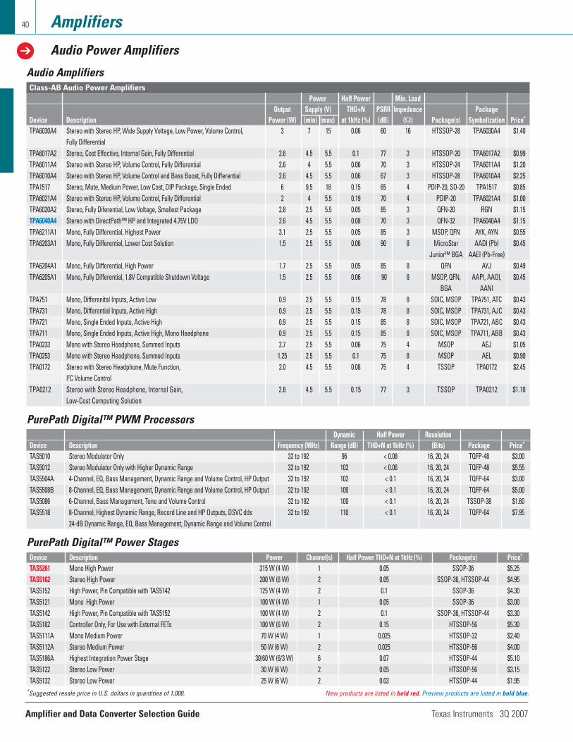
Amplifier and Data Converter Selection Guide Texas Instruments 3Q 2007
Amplifiers
Audio Power Amplifiers
40
Audio AmplifiersClass-AB Audio Power Amplifiers
Power Half Power Min. Load Output Supply (V) THD+N PSRR Impedance Package
Device Description Power (W) (min) (max) at 1kHz (%) (dB) (Ω) Package(s) Symbolization Price*
TPA6030A4 Stereo with Stereo HP, Wide Supply Voltage, Low Power, Volume Control, 3 7 15 0.06 60 16 HTSSOP-28 TPA6030A4 $1.40Fully Differential
TPA6017A2 Stereo, Cost Effective, Internal Gain, Fully Differential 2.6 4.5 5.5 0.1 77 3 HTSSOP-20 TPA6017A2 $0.99TPA6011A4 Stereo with Stereo HP, Volume Control, Fully Differential 2.6 4 5.5 0.06 70 3 HTSSOP-24 TPA6011A4 $1.20TPA6010A4 Stereo with Stereo HP, Volume Control and Bass Boost, Fully Differential 2.6 4.5 5.5 0.06 67 3 HTSSOP-28 TPA6010A4 $2.25TPA1517 Stereo, Mute, Medium Power, Low Cost, DIP Package, Single Ended 6 9.5 18 0.15 65 4 PDIP-20, SO-20 TPA1517 $0.85TPA6021A4 Stereo with Stereo HP, Volume Control, Fully Differential 2 4 5.5 0.19 70 4 PDIP-20 TPA6021A4 $1.00TPA6020A2 Stereo, Fully Diferential, Low Voltage, Smallest Package 2.8 2.5 5.5 0.05 85 3 QFN-20 RGN $1.15TPA6040A4 Stereo with DirectPath™ HP and Integrated 4.75V LDO 2.6 4.5 5.5 0.08 70 3 QFN-32 TPA6040A4 $1.15TPA6211A1 Mono, Fully Differential, Highest Power 3.1 2.5 5.5 0.05 85 3 MSOP, QFN AYK, AYN $0.55TPA6203A1 Mono, Fully Differential, Lower Cost Solution 1.5 2.5 5.5 0.06 90 8 MicroStar AADI (Pb) $0.45
Junior™ BGA AAEI (Pb-Free)TPA6204A1 Mono, Fully Differential, High Power 1.7 2.5 5.5 0.05 85 8 QFN AYJ $0.49TPA6205A1 Mono, Fully Differential, 1.8V Compatible Shutdown Voltage 1.5 2.5 5.5 0.06 90 8 MSOP, QFN, AAPI, AAOI, $0.45
BGA AANITPA751 Mono, Differenital Inputs, Active Low 0.9 2.5 5.5 0.15 78 8 SOIC, MSOP TPA751, ATC $0.43TPA731 Mono, Differential Inputs, Active High 0.9 2.5 5.5 0.15 78 8 SOIC, MSOP TPA731, AJC $0.43TPA721 Mono, Single Ended Inputs, Active High 0.9 2.5 5.5 0.15 85 8 SOIC, MSOP TPA721, ABC $0.43TPA711 Mono, Single Ended Inputs, Active High, Mono Headphone 0.9 2.5 5.5 0.15 85 8 SOIC, MSOP TPA711, ABB $0.43TPA0233 Mono with Stereo Headphone, Summed Inputs 2.7 2.5 5.5 0.06 75 4 MSOP AEJ $1.05TPA0253 Mono with Stereo Headphone, Summed Inputs 1.25 2.5 5.5 0.1 75 8 MSOP AEL $0.90TPA0172 Stereo with Stereo Headphone, Mute Function, 2.0 4.5 5.5 0.08 75 4 TSSOP TPA0172 $2.45
I2C Volume ControlTPA0212 Stereo with Stereo Headphone, Internal Gain, 2.6 4.5 5.5 0.15 77 3 TSSOP TPA0212 $1.10
Low-Cost Computing Solution
PurePath Digital™ PWM ProcessorsDynamic Half Power Resolution
Device Description Frequency (MHz) Range (dB) THD+N at 1kHz (%) (Bits) Package Price*
TAS5010 Stereo Modulator Only 32 to 192 96 < 0.08 16, 20, 24 TQFP-48 $3.00TAS5012 Stereo Modulator Only with Higher Dynamic Range 32 to 192 102 < 0.06 16, 20, 24 TQFP-48 $5.55TAS5504A 4-Channel, EQ, Bass Management, Dynamic Range and Volume Control, HP Output 32 to 192 102 < 0.1 16, 20, 24 TQFP-64 $3.00TAS5508B 8-Channel, EQ, Bass Management, Dynamic Range and Volume Control, HP Output 32 to 192 100 < 0.1 16, 20, 24 TQFP-64 $5.00TAS5086 6-Channel, Bass Management, Tone and Volume Control 32 to 192 100 < 0.1 16, 20, 24 TSSOP-38 $1.60TAS5518 8-Channel, Highest Dynamic Range, Record Line and HP Outputs, DSVC dds 32 to 192 110 < 0.1 16, 20, 24 TQFP-64 $7.95
24-dB Dynamic Range, EQ, Bass Management, Dynamic Range and Volume Control
PurePath Digital™ Power StagesDevice Description Power Channel(s) Half Power THD+N at 1kHz (%) Package(s) Price*
TAS5261 Mono High Power 315 W (4 W) 1 0.05 SSOP-36 $5.25TAS5162 Stereo High Power 200 W (6 W) 2 0.05 SSOP-36, HTSSOP-44 $4.95TAS5152 High Power, Pin Compatible with TAS5142 125 W (4 W) 2 0.1 SSOP-36 $4.30TAS5121 Mono High Power 100 W (4 W) 1 0.05 SSOP-36 $3.00TAS5142 High Power, Pin Compatible with TAS5152 100 W (4 W) 2 0.1 SSOP-36, HTSSOP-44 $3.30TAS5182 Controller Only, For Use with External FETs 100 W (6 W) 2 0.15 HTSSOP-56 $5.30TAS5111A Mono Medium Power 70 W (4 W) 1 0.025 HTSSOP-32 $2.40TAS5112A Stereo Medium Power 50 W (6 W) 2 0.025 HTSSOP-56 $4.00TAS5186A Highest Integration Power Stage 30/60 W (6/3 W) 6 0.07 HTSSOP-44 $5.10TAS5122 Stereo Low Power 30 W (6 W) 2 0.05 HTSSOP-56 $3.15TAS5132 Stereo Low Power 25 W (6 W) 2 0.03 HTSSOP-44 $1.95
*Suggested resale price in U.S. dollars in quantities of 1,000. New products are listed in bold red. Preview products are listed in bold blue.
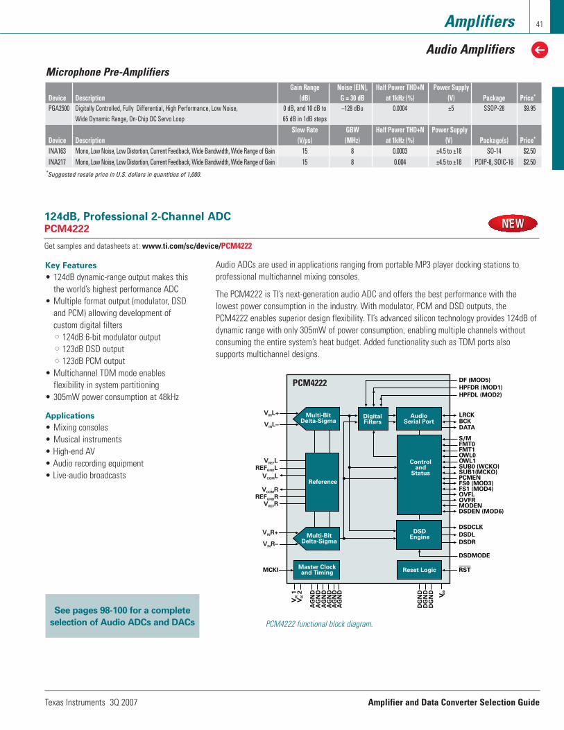
Texas Instruments 3Q 2007 Amplifier and Data Converter Selection Guide
Amplifiers
Audio Amplifiers
41
Controland
Status
Reset Logic
DSDEngineMulti-Bit
Delta-Sigma
Multi-BitDelta-Sigma
Reference
AudioSerial Port
LRCKBCKDATA
DF (MOD5)
HPFDR (MOD1)
HPFDL (MOD2)
DigitalFilters
S/MFMT0FMT1OWL0OWL1SUB0 (WCKO)SUB1(MCKO)PCMENFS0 (MOD3)FS1 (MOD4)OVFLOVFRMODENDSDEN (MOD6)
DG
ND
DG
ND
DG
ND
VD
D
DSDL
DSDCLK
DSDR
DSDMODE
RSTMCKIMaster Clockand Timing
VCC
1V
CC2
AG
ND
AG
ND
AG
ND
AG
ND
AG
ND
AG
ND
VINR–
VINR+
VREFR
VINL–
VINL+
VCOML
VREFL
REFGNDL
REFGNDR
VCOMR
124dB, Professional 2-Channel ADCPCM4222
Get samples and datasheets at: www.ti.com/sc/device/PCM4222
PCM4222 functional block diagram.
Key Features
• 124dB dynamic-range output makes thisthe world’s highest performance ADC
• Multiple format output (modulator, DSDand PCM) allowing development of custom digital filters•• 124dB 6-bit modulator output•• 123dB DSD output•• 123dB PCM output
• Multichannel TDM mode enables flexibility in system partitioning
• 305mW power consumption at 48kHz
Applications
• Mixing consoles• Musical instruments• High-end AV• Audio recording equipment• Live-audio broadcasts
Audio ADCs are used in applications ranging from portable MP3 player docking stations to professional multichannel mixing consoles.
The PCM4222 is TI’s next-generation audio ADC and offers the best performance with the lowest power consumption in the industry. With modulator, PCM and DSD outputs, thePCM4222 enables superior design flexibility. TI’s advanced silicon technology provides 124dB ofdynamic range with only 305mW of power consumption, enabling multiple channels withoutconsuming the entire system’s heat budget. Added functionality such as TDM ports also supports multichannel designs.
Microphone Pre-AmplifiersGain Range Noise (EIN), Half Power THD+N Power Supply
Device Description (dB) G = 30 dB at 1kHz (%) (V) Package Price*
PGA2500 Digitally Controlled, Fully Differential, High Performance, Low Noise, 0 dB, and 10 dB to –128 dBu 0.0004 ±5 SSOP-28 $9.95Wide Dynamic Range, On-Chip DC Servo Loop 65 dB in 1dB steps
Slew Rate GBW Half Power THD+N Power SupplyDevice Description (V/µs) (MHz) at 1kHz (%) (V) Package(s) Price*
INA163 Mono, Low Noise, Low Distortion, Current Feedback, Wide Bandwidth, Wide Range of Gain 15 8 0.0003 ±4.5 to ±18 SO-14 $2.50INA217 Mono, Low Noise, Low Distortion, Current Feedback, Wide Bandwidth, Wide Range of Gain 15 8 0.004 ±4.5 to ±18 PDIP-8, SOIC-16 $2.50
*Suggested resale price in U.S. dollars in quantities of 1,000.
PCM4222
See pages 98-100 for a complete
selection of Audio ADCs and DACs
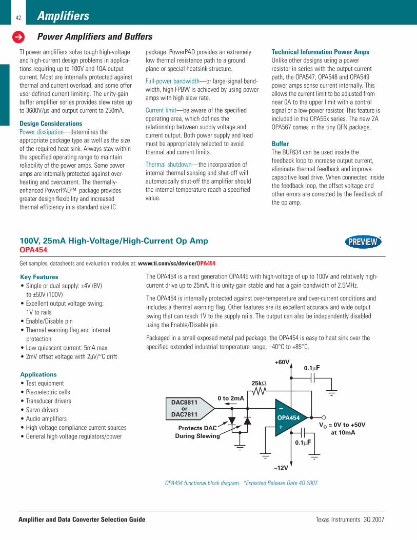
Amplifier and Data Converter Selection Guide Texas Instruments 3Q 2007
42 Amplifiers
Power Amplifiers and Buffers
TI power amplifiers solve tough high-voltageand high-current design problems in applica-tions requiring up to 100V and 10A output current. Most are internally protected againstthermal and current overload, and some offeruser-defined current limiting. The unity-gainbuffer amplifier series provides slew rates upto 3600V/µs and output current to 250mA.
Design ConsiderationsPower dissipation—determines the appropriate package type as well as the sizeof the required heat sink. Always stay withinthe specified operating range to maintainreliability of the power amps. Some poweramps are internally protected against over-heating and overcurrent. The thermally-enhanced PowerPAD™ package providesgreater design flexibility and increased thermal efficiency in a standard size IC
package. PowerPAD provides an extremelylow thermal resistance path to a groundplane or special heatsink structure.
Full-power bandwidth—or large-signal band-width, high FPBW is achieved by using poweramps with high slew rate.
Current limit—be aware of the specified operating area, which defines the relationship between supply voltage and current output. Both power supply and loadmust be appropriately selected to avoidthermal and current limits.
Thermal shutdown—the incorporation ofinternal thermal sensing and shut-off willautomatically shut-off the amplifier shouldthe internal temperature reach a specifiedvalue.
Technical Information Power AmpsUnlike other designs using a power resistor in series with the output currentpath, the OPA547, OPA548 and OPA549power amps sense current internally. Thisallows the current limit to be adjusted fromnear 0A to the upper limit with a control signal or a low-power resistor. This feature isincluded in the OPA56x series. The new 2AOPA567 comes in the tiny QFN package.
BufferThe BUF634 can be used inside the feedback loop to increase output current,eliminate thermal feedback and improvecapacitive load drive. When connected insidethe feedback loop, the offset voltage andother errors are corrected by the feedback ofthe op amp.
100V, 25mA High-Voltage/High-Current Op AmpOPA454
Get samples, datasheets and evaluation modules at: www.ti.com/sc/device/OPA454
OPA454 functional block diagram. *Expected Release Date 4Q 2007.
Key Features
• Single or dual supply: ±4V (8V) to ±50V (100V)
• Excellent output voltage swing: 1V to rails
• Enable/Disable pin• Thermal warning flag and internal
protection• Low quiescent current: 5mA max• 2mV offset voltage with 2µV/°C drift
Applications
• Test equipment• Piezoelectric cells• Transducer drivers• Servo drivers• Audio amplifiers• High voltage compliance current sources• General high voltage regulators/power
The OPA454 is a next generation OPA445 with high-voltage of up to 100V and relatively high-current drive up to 25mA. It is unity-gain stable and has a gain-bandwidth of 2.5MHz.
The OPA454 is internally protected against over-temperature and over-current conditions andincludes a thermal warning flag. Other features are its excellent accuracy and wide outputswing that can reach 1V to the supply rails. The output can also be independently disabledusing the Enable/Disable pin.
Packaged in a small exposed metal pad package, the OPA454 is easy to heat sink over the specified extended industrial temperature range, –40°C to +85°C.
OPA454
0 to 2mA
+60V
25kΩ
–12V
VO = 0V to +50V
at 10mA
0.1µF
0.1µF
Protects DAC
During Slewing
DAC8811or
DAC7811
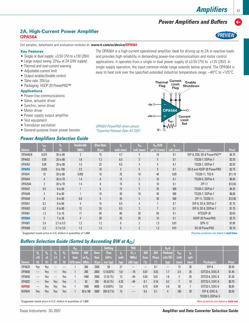
Texas Instruments 3Q 2007 Amplifier and Data Converter Selection Guide
Amplifiers
Power Amplifiers and Buffers
43
OPA564
Thermal Flag
CurrentLimitFlag
Enable Shutdown
RSET
V–
+In
–In
CurrentLimitSet
2A, High-Current Power AmplifierOPA564
Get samples, datasheets and evaluation modules at: www.ti.com/sc/device/OPA564
OPA564 PowerPAD-down pinout.*Expected Release Date 4Q 2007.
Key Features
• Single or dual supply: ±3.5V (7V) to ±13V (26V)• Large output swing: 22VPP at 2A (24V supply)• Thermal and over-current warning• Adjustable current limit• Output enable/disable control• Slew rate: 20V/µs• Packaging: HSOP-20 PowerPAD™Applications
• Power-line communications• Valve, actuator driver• Synchro, servo driver• Motor driver• Power supply output amplifier• Test equipment• Transducer excitation• General-purpose linear power booster
The OPA564 is a high-current operational amplifier ideal for driving up to 2A in reactive loadsand provides high reliability in demanding power-line communications and motor control applications. It operates from a single or dual power supply of ±3.5V (7V) to ±13V (26V). In single supply operation, the input common-mode range extends below ground. The OPA564 iseasy to heat sink over the specified extended industrial temperature range, –40°C to +125°C.
Power Amplifiers Selection GuideIOUT VS Bandwidth Slew Rate IQ VOS VOS Drift IB
Device (A) (V) (MHz) (V/µs) (mA) (max) (mV) (max) (µV/°C) (max) (nA) (max) Package(s) Price*
OPA445/B 0.015 20 to 90 2 15 4.7 5 10 0.1 DIP-8, SO8, SO-8 PowerPAD™ $4.75 OPA452 0.05 20 to 80 1.8 7.2 6.5 3 5 0.1 TO220-7, DDPak-7 $2.55 OPA453 0.05 20 to 80 7.5 23 6.5 3 5 0.1 TO220-7, DDPak-7 $2.55 OPA454 0.025 8 to 100 2.5 10 5 5 5 0.1 SO-8 and HSOP-20 PowerPAD $2.75 OPA541 10 20 to 80 0.055 10 25 10 40 0.05 TO220-11, TO3-8 $11.10 OPA544 4 20 to 70 1.4 8 15 5 10 0.1 TO220-5, DDPak-5 $6.85 OPA2544 2 20 to 70 1.4 8 15 5 10 0.1 ZIP-11 $12.00 OPA547 0.5 8 to 60 1 6 15 5 25 500 TO220-7, DDPak-7 $4.35 OPA548 3 8 to 60 1 10 20 10 30 500 TO220-7, DDPak-7 $6.00 OPA549 8 8 to 60 0.9 9 35 5 20 500 ZIP-11, TO220-11 $12.00 OPA551 0.2 8 to 60 3 15 8.5 3 7 0.1 DIP-8, SO-8, DDPak-7 $1.75 OPA552 0.2 8 to 60 12 24 8.5 3 7 0.1 DIP-8, SO-8, DDPak-7 $1.75 OPA561 1.2 7 to 16 17 50 60 20 50 0.1 HTSSOP-20 $2.65 OPA564 2 7 to 26 4 20 35 20 10 0.1 HSOP-20 PowerPAD $2.75 OPA567 2.4 2.7 to 5.5 1.2 1.2 6 2 1.3 0.01 QFN-12 $1.85 OPA569 2.2 2.7 to 5.5 1.2 1.2 6 2 1.3 0.01 SO-20 PowerPAD $3.10 *Suggested resale price in U.S. dollars in quantities of 1,000. Preview products are listed in bold blue.
Buffers Selection Guide (Sorted by Ascending BW at ACL)ACL Settling THD VN at
VS VS VS VS Stable BW Slew Time IQ (FC = Diff Diff Flatband VOS IB
±15 ±5 3.3 5 Gain at ACL Rate 0.01% (mA) 1MHz) Gain Phase (nV/ Hz) (mV) (µA)Device (V) (V) (V) (V) (V/V) (min) (MHz) (V/µs) (ns) (typ) (typ) (dB) (typ) (%) (°) (typ) (max) (max) Package(s) Price*
OPA633 Yes Yes — — 1 260 2500 50 21 — — 0.1 — 15 35 DIP-8 $5.45 OPA692 — Yes — Yes 1 280 2000 12 (0.02%) 5.8 –78 0.07 0.02 1.7 2.5 35 SOT23-6, SOIC-8 $1.45 OPA693 — Yes — Yes 1 1400 2500 12 (0.1%) 13 –84 0.03 0.01 1.8 2 35 SOT23-6, SOIC-8 $1.30 OPA832 — Yes Yes Yes 1 92 350 45 (0.1%) 4.25 –84 0.1 0.16 9.2 7 10 SOT23-5, SOIC-8 $0.70 BUF602 — Yes Yes Yes 1 1000 8000 6 (0.05%) 5.8 — 0.15 0.04 4.8 30 7 SOT23-5, SOIC-8 $0.85 BUF634 Yes Yes Yes Yes 1 30 to 180 2000 200 (0.1%) 15 — 0.4 0.1 4 100 20 DIP-8, SOIC-8, $3.05
TO220-5, DDPak-5 *Suggested resale price in U.S. dollars in quantities of 1,000. New products are listed in bold red.
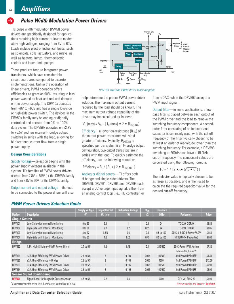
Amplifier and Data Converter Selection Guide Texas Instruments 3Q 2007
44 Amplifiers
Pulse Width Modulation Power Drivers
from a DAC, while the DRV592 accepts aPWM input signal.
Output filter—in some applications, a low-pass filter is placed between each output ofthe PWM driver and the load to remove theswitching frequency components. A second-order filter consisting of an inductor andcapacitor is commonly used, with the cut-offfrequency of the filter typically chosen to beat least an order of magnitude lower than theswitching frequency. For example, a DRV593switching at 500kHz can have a 15.9kHz cut-off frequency. The component values arecalculated using the following formula:
FC = 1 / [ 2 •π• (√(L • C) ) ]
The inductor value is typically chosen to beas large as possible, and is then used to calculate the required capacitor value for thedesired cut-off frequency.
TI’s pulse width modulation (PWM) powerdrivers are specifically designed for applica-tions requiring high current at low to moder-ately high voltages, ranging from 5V to 60V.Loads include electromechanical loads, suchas solenoids, coils, actuators, and relays, aswell as heaters, lamps, thermoelectric coolers and laser diode pumps.
These products feature integrated powertransistors, which save considerable circuit board area compared to discreteimplementations. Unlike the operation of linear drivers, PWM operation offers efficiencies as great as 90%, resulting in lesspower wasted as heat and reduced demandon the power supply. The DRV10x operatesfrom +8V to +60V and has a single low-sideor high-side power switch. The devices in theDRV59x family may be analog or digitallycontrolled and operate from 0% to 100%duty cycles. The DRV59x operates on +2.8Vto +5.5V and has internal H-bridge outputswitches in series with the load, allowing for bi-directional current flow from a singlepower supply.
Design Considerations
Supply voltage—selection begins with thepower supply voltages available in the system. TI’s families of PWM power driversoperate from 2.8V to 5.5V for the DRV59x familyand from 2.8V to 60V for the DRV10x family.
Output current and output voltage—the loadto be connected to the power driver will also
help determine the proper PWM power driversolution. The maximum output currentrequired by the load should be known. Themaximum output voltage capability of thedriver may be calculated as follows:
VO (max) = VS – [ IO (max) • 2 • RDS(ON) ]
Efficiency—a lower on-resistance (RON) ofthe output power transistors will yieldgreater efficiency. Typically, RDS(ON) is specified per transistor. In an H-bridge outputconfiguration, two output transistors are inseries with the load. To quickly estimate theefficiency, use the following equation:
Efficiency = RL / [ RL + ( 2 • RDS(ON) ) ]
Analog or digital control—TI offers both H-bridge and single-sided drivers. TheDRV590, DRV591, DRV593 and DRV594 eachaccept a DC voltage input signal, either froman analog control loop (i.e., PID controller) or
Delay Adj
CDR
PWM
Input
On
Off
Thermal Shutdown
Over Current
Status OKFlag
Coil
Cooler
Heater
Lamp
+VS
OscillatorVREF
PWM
GND
OUT
Flyback
DiodeDMOS
DMOS
ESD
Osc FreqAdj
Duty CycleAdj
RFREQ
Delay
DRV103
DRV103 low-side PWM driver block diagram.
PWM Power Drivers Selection GuideSupply Voltage Output Current Saturation Voltage RON Frequency
Device Description (V) (A) (typ) (V) (Ω) (kHz) Package(s) Price*
Single SwitchDRV101 Low-Side with Internal Monitoring 9 to 60 2.3 1 0.8 24 TO-220, DDPAK $3.85 DRV102 High-Side with Internal Monitoring 8 to 60 2.7 2.2 0.95 24 TO-220, DDPAK $3.85 DRV103 Low-Side with Internal Monitoring 8 to 32 1.5/3 0.6 0.9 0.5 to 100 SOIC-8, SOIC-8 PowerPAD™ $1.60 DRV104 High-Side with Internal Monitoring 8 to 32 1.2 0.65 0.45 0.5 to 100 HTSSOP-14 PowerPAD $1.60 BridgeDRV590 1.2A, High-Efficiency PWM Power Driver 2.7 to 5.5 1.2 0.48 0.4 250/500 SOIC-PowerPAD, 4x4mm $7.30
MicroStar Junior™DRV591 ±3A, High-Efficiency PWM Power Driver 2.8 to 5.5 3 0.195 0.065 100/500 9x9 PowerPAD QFP $6.30 DRV592 ±3A, High-Efficiency H-Bridge 2.8 to 5.5 3 0.195 0.065 1000 9x9 PowerPAD QFP $12.50 DRV593 ±3A, High-Efficiency PWM Power Driver 2.8 to 5.5 3 0.195 0.065 100/500 9x9 PowerPAD QFP $5.90 DRV594 ±3A, High-Efficiency PWM Power Driver 2.8 to 5.5 3 0.195 0.065 100/500 9x9 PowerPAD QFP $5.90Sensor Signal ConditioningDRV401 Signal Cond. for Magnetic Current Sensor 4.5 to 5.5 0.2 0.4 — 2000 QFN-20, SOIC-20 $1.90
*Suggested resale price in U.S. dollars in quantities of 1,000. New products are listed in bold red.
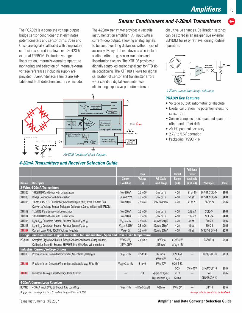
Texas Instruments 3Q 2007 Amplifier and Data Converter Selection Guide
Amplifiers
Sensor Conditioners and 4-20mA Transmitters
45
The 4-20mA transmitter provides a versatileinstrumentation amplifier (IA) input with acurrent-loop output, allowing analog signalsto be sent over long distances without loss ofaccuracy. Many of these devices also includescaling, offsetting, sensor excitation and linearization circuitry. The XTR108 provides adigitally controlled analog signal path for RTD sig-nal conditioning. The XTR108 allows for digitalcalibration of sensor and transmitter errorsvia a standard digital serial interface, eliminating expensive potentiometers or
The PGA309 is a complete voltage outputbridge sensor conditioner that eliminatespotentiometers and sensor trims. Span andOffset are digitally calibrated with temperaturecoefficients stored in a low-cost, SOT23-5,external EEPROM. Excitation voltage linearization, internal/external temperaturemonitoring and selection of internal/externalvoltage references including supply are provided. Over/Under scale limits are set-table and fault detection circuitry is included.
circuit value changes. Calibration settingscan be stored in an inexpensive external EEPROM for easy retrieval during routineoperation.
VLOOP
XTR
RTD
4-20mA
4-20mA transmitter design solutions.
PGA309 Key Features• Voltage output: ratiometric or absolute• Digital calibration: no potentiometers, no
sensor trim• Sensor compensation: span and span drift,
offset and offset drift• <0.1% post-cal accuracy• 2.7V to 5.5V operation• Packaging: TSSOP-16
Linearization
Circuit
Ref
Linearization
DAC
Over/Under
Scale Limiter
Auto-Zero
PGA
Fault
Monitor
Analog Sensor Linearization
VEXC
Analog Signal Conditioning
Digital Temperature
CompensationInt
Temp
Temp
ADCExt Temp
Control Register
Interface CircuitryEEPROM
(SOT23-5)
DIGITAL CAL
Linear
VS
VS
T
VOUT
PGA309 functional block diagram.
4-20mA Transmitters and Receiver Selection GuideAdditional
Loop Output PowerSensor Voltage Full-Scale Range Available
Device Description Excitation (V) Input Range (mA) (V at mA) Package(s) Price*
2-Wire, 4-20mA TransmittersXTR105 100Ω RTD Conditioner with Linearization Two 800µA 7.5 to 36 5mV to 1V 4-20 5.1 at 0.5 DIP-14, SOIC-14 $4.00 XTR106 Bridge Conditioner with Linearization 5V and 2.5V 7.5 to 36 5mV to 1V 4-20 5.1 at 1 DIP-14, SOIC-14 $4.00 XTR108 10Ω to 10kΩ RTD Conditioner, 6-Channel Input Mux, Extra Op Amp Can Two 500µA 7.5 to 24 5mV to 320mV 4-20 5.1 at 2.1 SSOP-24 $3.35
Convert to Voltage Sensor Excitation, Calibration Stored in External EEPROMXTR112 1kΩ RTD Conditioner with Linearization Two 250µA 7.5 to 36 5mV to 1V 4-20 5.05 at 1 SOIC-14 $4.00 XTR114 10kΩ RTD Conditioner with Linearization Two 100µA 7.5 to 36 5mV to 1V 4-20 5.05 at 1 SOIC-14 $4.00 XTR115 IIN to IOUT Converter, External Resistor Scales VIN to IIN VREF = 2.5V 7.5 to 36 40µA to 250µA 4-20 4.9 at 1 SOIC-8 $1.05 XTR116 IIN to IOUT Converter, External Resistor Scales VIN to IIN VREF = 4.096V 7.5 to 36 40µA to 250µA 4-20 4.9 at 1 SOIC-8 $1.05 XTR117 Current Loop, 7.5 to 40V, 5V Voltage Regulator VREG= 5V 7.5 to 40 40µA to 250µA 4-20 4.9 at 1 MSOP-8, DFN-8 $0.90 Bridge Conditioner with Digital Calibration for Linearization, Span and Offset Over TemperaturePGA309 Complete Digitally Calibrated Bridge Sensor Conditioner, Voltage Output, VEXC = VS, 2.7 to 5.5 1mV/V to 0.05V-4.9V — TSSOP-16 $3.40
Calibration Stored in External EEPROM, One-Wire/Two-Wire Interface 2.5V 4.096V 245mV/V at VS = +5VIndustrial Current/Voltage DriversXTR110 Precision V-to-I Converter/Transmitter, Selectable I/O Ranges VREF = 10V 13.5 to 40 0V to 5V, 0-20, 4-20 — DIP-16, SOL-16 $7.10
0V to 10V 5-25XTR111 Precision V-to-I Converter/Transmitter, Adjustable VREG 3V to 15V VREG = 3 to 15V 8 to 40 0V to 12V 0-20, 4-20,
5-25 3V to 15V DFN/MSOP-10 $1.45 XTR300 Industrial Analog Current/Voltage Output Driver — <34 V(–)+3 to V(+)–3 ±17V — 5x5 $2.45
Dig. selected VO≤ ±24mA QFN/TSSOP-204-20mA Current Loop ReceiverRCV420 4-20mA Input, 0V to 5V Output, 1.5V Loop Drop VREF = 10V +11.5/–5 to ±18 4-20mA 0V to 5V — DIP-16 $3.55
*Suggested resale price in U.S. dollars in quantities of 1,000. New products are listed in bold red.
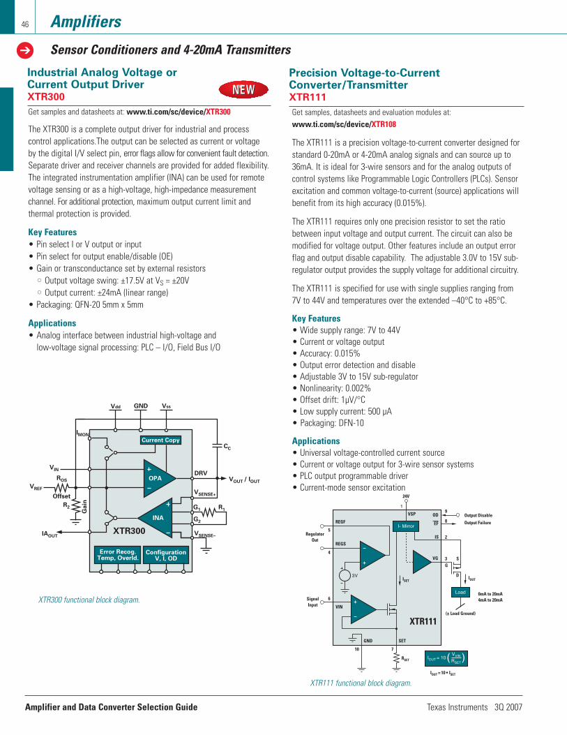
Amplifier and Data Converter Selection Guide Texas Instruments 3Q 2007
Amplifiers
Sensor Conditioners and 4-20mA Transmitters
46
Industrial Analog Voltage orCurrent Output DriverXTR300
XTR300 functional block diagram.
Get samples and datasheets at: www.ti.com/sc/device/XTR300
The XTR300 is a complete output driver for industrial and process control applications.The output can be selected as current or voltageby the digital I/V select pin, error flags allow for convenient fault detection.Separate driver and receiver channels are provided for added flexibility.The integrated instrumentation amplifier (INA) can be used for remote voltage sensing or as a high-voltage, high-impedance measurementchannel. For additional protection, maximum output current limit and thermal protection is provided.
Key Features• Pin select I or V output or input• Pin select for output enable/disable (OE)• Gain or transconductance set by external resistors
•• Output voltage swing: ±17.5V at VS = ±20V•• Output current: ±24mA (linear range)
• Packaging: QFN-20 5mm x 5mm
Applications• Analog interface between industrial high-voltage and
low-voltage signal processing: PLC – I/O, Field Bus I/O
XTR111 functional block diagram.
Current Copy
OPA
INA
DRV
CC
VOUT / IOUT
VSENSE+
G1
G2
R1
VSENSE–
Error Recog.Temp, Overld.
ConfigurationV, I, OD
IAOUT
VIN
VREF
ROS
Offset
R2
Ga
in
IMON
Vdd GND Vss
XTR300
Precision Voltage-to-CurrentConverter/TransmitterXTR111
Get samples, datasheets and evaluation modules at:www.ti.com/sc/device/XTR108
The XTR111 is a precision voltage-to-current converter designed forstandard 0-20mA or 4-20mA analog signals and can source up to36mA. It is ideal for 3-wire sensors and for the analog outputs ofcontrol systems like Programmable Logic Controllers (PLCs). Sensorexcitation and common voltage-to-current (source) applications willbenefit from its high accuracy (0.015%).
The XTR111 requires only one precision resistor to set the ratiobetween input voltage and output current. The circuit can also bemodified for voltage output. Other features include an output errorflag and output disable capability. The adjustable 3.0V to 15V sub-regulator output provides the supply voltage for additional circuitry.
The XTR111 is specified for use with single supplies ranging from7V to 44V and temperatures over the extended –40°C to +85°C.
Key Features• Wide supply range: 7V to 44V• Current or voltage output• Accuracy: 0.015% • Output error detection and disable • Adjustable 3V to 15V sub-regulator• Nonlinearity: 0.002%• Offset drift: 1µV/°C• Low supply current: 500 µA• Packaging: DFN-10
Applications• Universal voltage-controlled current source• Current or voltage output for 3-wire sensor systems• PLC output programmable driver• Current-mode sensor excitation
3V
REGF
RegulatorOut
SignalInput
REGS
24V
I- Mirror
VSP
19
8
2
3G
S
D
VG
IS
Output Disable
Output Failure
0mA to 20mA4mA to 20mA
OD
EF
VIN
6
4
5
RSET
ISET
SET
710
GND
IOUT = 10( )VVIN
RSET
IOUT = 10 • ISET
Load
IOUT
(± Load Ground)
XTR111
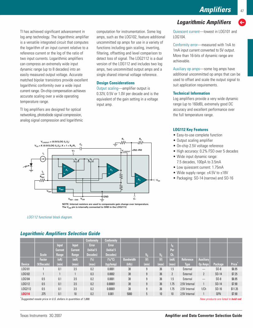
Texas Instruments 3Q 2007 Amplifier and Data Converter Selection Guide
Amplifiers
Logarithmic Amplifiers
47
Q1 Q2
CC
I1
VREF – GND
NOTE: Internal resistors are used to compensate gain change over temperature.
The VCM pin is internally connected to GND in the LOG2112.
VO3
V+
GND
VLOGOUT = (0.5V)LOG (I1/I2)
VO3 = K (0.5V)LOG (I1/I2), K = 1 + R2/R1
A3
R2R1
VREF
RREF
+IN3 VLOGOUT
–IN3
V–VCM
I2
VREF
A2A1
LOG112 functional block diagram.
TI has achieved significant advancement inlog amp technology. The logarithmic amplifieris a versatile integrated circuit that computesthe logarithm of an input current relative to areference current or the log of the ratio oftwo input currents. Logarithmic amplifierscan compress an extremely wide inputdynamic range (up to 8 decades) into an easily measured output voltage. Accuratematched bipolar transistors provide excellentlogarithmic conformity over a wide input current range. On-chip compensation achievesaccurate scaling over a wide operating temperature range.
TI log amplifiers are designed for optical networking, photodiode signal compression,analog signal compression and logarithmic
computation for instrumentation. Some logamps, such as the LOG102, feature additionaluncommitted op amps for use in a variety offunctions including gain scaling, inverting, filtering, offsetting and level comparison todetect loss of signal. The LOG2112 is a dualversion of the LOG112 and includes two logamps, two uncommitted output amps and asingle shared internal voltage reference.
Design ConsiderationsOutput scaling—amplifier output is 0.32V, 0.5V or 1.0V per decade and is theequivalent of the gain setting in a voltageinput amp.
Quiescent current—lowest in LOG101 andLOG104.
Conformity error—measured with 1nA to1mA input current converted to 5V output.More than 16-bits of dynamic range areachievable.
Auxiliary op amps—some log amps haveadditional uncommitted op amps that can beused to offset and scale the output signal tosuit application requirements.
Technical InformationLog amplifiers provide a very wide dynamicrange (up to 160dB), extremely good DC accuracy and excellent performance over the full temperature range.
LOG112 Key Features• Easy-to-use complete function• Output scaling amplifier• On-chip 2.5V voltage reference• High accuracy: 0.2% FSO over 5 decades• Wide input dynamic range:
7.5 decades, 100pA to 3.5mA• Low quiescent current: 1.75mA• Wide supply range: ±4.5V to ±18V• Packaging: SO-14 (narrow) and SO-16
Logarithmic Amplifiers Selection GuideConformity Conformity
Input Input Error Error IQ
Current Current (Initial 5 (Initial 5 PerScale Range Range Decades) Decades) VS VS Ch.Factor (nA) (mA) (%) (%/°C) Bandwidth (V) (V) (mA) Reference Auxiliary
Device (V/Decade) (min) (max) (max) (typ/temp) (kHz) (min) (max) (max) Type Op Amps Package Price*
LOG101 1 0.1 3.5 0.2 0.0001 38 9 36 1.5 External — SO-8 $6.95 LOG102 1 1 1 0.3 0.0002 38 9 36 2 External 2 SO-14 $7.25 LOG104 0.5 0.1 3.5 0.2 0.0001 38 9 36 1.5 External — SO-8 $6.95 LOG112 0.5 0.1 3.5 0.2 0.00001 38 9 36 1.75 2.5V Internal 1 SO-14 $7.90 LOG2112 0.5 0.1 3.5 0.2 0.00001 38 9 36 1.75 2.5V Internal 1/Ch SO-16 $11.35 LOG114 .375 0.1 10 0.2 0.001 5000 5 10 10 2.5V Internal 1 QFN $7.90
*Suggested resale price in U.S. dollars in quantities of 1,000. New products are listed in bold red.
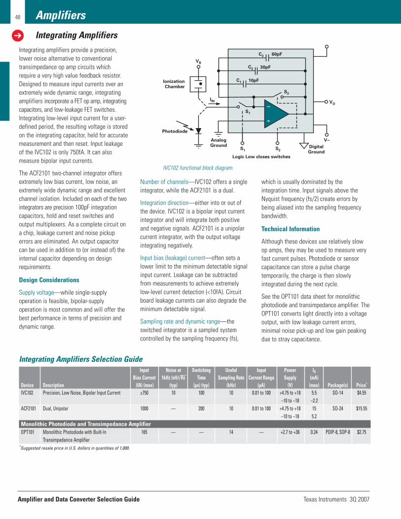
Amplifier and Data Converter Selection Guide Texas Instruments 3Q 2007
48 Amplifiers
Integrating Amplifiers
Integrating amplifiers provide a precision,lower noise alternative to conventional transimpedance op amp circuits whichrequire a very high value feedback resistor.Designed to measure input currents over anextremely wide dynamic range, integratingamplifiers incorporate a FET op amp, integratingcapacitors, and low-leakage FET switches.Integrating low-level input current for a user-defined period, the resulting voltage is storedon the integrating capacitor, held for accuratemeasurement and then reset. Input leakageof the IVC102 is only 750fA. It can also measure bipolar input currents.
The ACF2101 two-channel integrator offersextremely low bias current, low noise, anextremely wide dynamic range and excellentchannel isolation. Included on each of the twointegrators are precision 100pF integrationcapacitors, hold and reset switches and output multiplexers. As a complete circuit ona chip, leakage current and noise pickuperrors are eliminated. An output capacitorcan be used in addition to (or instead of) theinternal capacitor depending on designrequirements.
Design Considerations
Supply voltage—while single-supply operation is feasible, bipolar-supply operation is most common and will offer thebest performance in terms of precision anddynamic range.
Number of channels—IVC102 offers a singleintegrator, while the ACF2101 is a dual.
Integration direction—either into or out ofthe device. IVC102 is a bipolar input currentintegrator and will integrate both positiveand negative signals. ACF2101 is a unipolarcurrent integrator, with the output voltageintegrating negatively.
Input bias (leakage) current—often sets alower limit to the minimum detectable signalinput current. Leakage can be subtractedfrom measurements to achieve extremelylow-level current detection (<10fA). Circuitboard leakage currents can also degrade theminimum detectable signal.
Sampling rate and dynamic range—theswitched integrator is a sampled system controlled by the sampling frequency (fs),
which is usually dominated by the integration time. Input signals above theNyquist frequency (fs/2) create errors bybeing aliased into the sampling frequencybandwidth.
Technical Information
Although these devices use relatively slow op amps, they may be used to measure veryfast current pulses. Photodiode or sensorcapacitance can store a pulse charge temporarily, the charge is then slowly integrated during the next cycle.
See the OPT101 data sheet for monolithicphotodiode and transimpedance amplifier. TheOPT101 converts light directly into a voltageoutput, with low leakage current errors, minimal noise pick-up and low gain peakingdue to stray capacitance.
IIN
VB
DigitalGround
AnalogGround
Logic Low closes switches
VO
V–
S1 S2
IonizationChamber
Photodiode
60pF
30pF
10pF
S1
C1
C2
C3
S2
IVC102 functional block diagram.
Integrating Amplifiers Selection GuideInput Noise at Switching Useful Input Power IQ
Bias Current 1kHz (nV/ Hz Time Sampling Rate Current Range Supply (mA)Device Description (fA) (max) (typ) (µs) (typ) (kHz) (µA) (V) (max) Package(s) Price*
IVC102 Precision, Low Noise, Bipolar Input Current ±750 10 100 10 0.01 to 100 +4.75 to +18 5.5 SO-14 $4.55 –10 to –18 –2.2
ACF2101 Dual, Unipolar 1000 — 200 10 0.01 to 100 +4.75 to +18 15 SO-24 $15.55 –10 to –18 5.2
Monolithic Photodiode and Transimpedance AmplifierOPT101 Monolithic Photodiode with Built-In 165 — — 14 — +2.7 to +36 0.24 PDIP-8, SOP-8 $2.75
Transimpedance Amplifier*Suggested resale price in U.S. dollars in quantities of 1,000.

Texas Instruments 3Q 2007 Amplifier and Data Converter Selection Guide
Amplifiers
Isolation Amplifiers
49
OSC
+
PWM
IN
POR
VREF
VREF
DC ChannelIsolation
Barrier
AC Channel
Input
+
Filter
BIAS POR
Data MUX(722 Only)
AC Detect
3-State
Output
Buffer
Filter
PWD
EN
OUT
Carrier
Detect
3.3V, High-Speed Digital Isolators
ISO721, ISO722
Get samples, datasheets, evaluation modules and app reports at: www.ti.com/ISO721 and www.ti.com/sc/device/ISO722
ISO721 functional block diagram.
Key Features• 4000V isolation• Fail-safe output• Signaling rate up to 100Mbps• UL 1577, IEC 60747-5-2 (VDE 0884,
Rev. 2), IEC 61010-1 and CSA Approved• 25kV/µs transient immunity
Applications• Industrial fieldbus• Servo monitoring and control
The ISO721 digital isolator is a logic input and output buffer separated by a silicon oxide (SiO2)insulation barrier that provides galvanic isolation of up to 4000V. Used in conjunction with isolated power supplies, the device prevents noise currents on a data bus or other circuits fromentering the local ground and interfering with or damaging sensitive circuitry.
A binary input signal is conditioned, translated to a balanced signal, then differentiated by thecapacitive isolation barrier. Across the isolation barrier, a differential comparator receives thelogic transition information, then sets or resets a flip-flop and the output circuit accordingly. Aperiodic update pulse is sent across the barrier to ensure the proper dc level of the output. Ifthis dc-refresh pulse is not received for more than 4µs, the input is assumed to be unpoweredor not functional and the fail-safe circuit drives the output to a logic high state.
There are many applications where it isdesirable, even essential, that a sensor nothave a direct (galvanic) electrical connectionwith the system to which it is supplying datain order to avoid either dangerous voltages orcurrents from one half of the system fromdamaging the other half. Such a system issaid to be "isolated", and the area whichpasses a signal without galvanic connectionsis known as an "isolation barrier".
Isolation barrier protection works in bothdirections, and may be needed in either halfof the system, sometimes both. Common applications requiring isolation protection are
those where sensors may accidentallyencounter high voltages and the system it isdriving must be protected. Or a sensor mayneed to be isolated from accidental high voltages arising downstream in order to protect its environment: examples includeprevention of explosive gas ignition causedby sparks at sensor locations or protectingpatients from electric shock by ECG, EEG andEMG test and monitoring equipment. TheECG application may require isolation barriersin both directions: the patient must be protected from the very high voltages(>7.5kV) applied by the defibrillator, and the
technician handling the device must be protected from unexpected feedback.
Applications for Isolation Amplifiers
• Sensor is at a high potential relative toother circuitry (or may become so underfault conditions)
• Sensor may not carry dangerous voltages,irrespective of faults in other circuitry (e.g.patient monitoring and intrinsically safe equipment for use with explosive gases)
• To break ground loops
Isolation Amplifiers Selection GuideIsolation Isolation Isolation Input Small-
Voltage Cont Voltage Pulse/ Mode Gain Offset Voltage SignalPeak (DC) Test Peak Rejection DC Nonlinearity Drift (±µV/°C) Bandwidth
Device Description (V) (V) (dB) (typ) (%) (max) (max) (kHz) (typ) Package(s) Price*
ISO122 1500VRMS Isolation, Buffer 1500 2400 140 0.05 200 50 DIP-16, SOIC-28 $9.40 ISO124 1500VRMS Isolation, Buffer 1500 2400 140 0.01 200 50 DIP-16, SOIC-28 $7.20 Digital Couplers
Isolation Isolation Peak Working Data Transient PropagationVoltage Cont Voltage Pulse/ Transient Voltage Rate Immunity Delay PWD ICCQ
Peak (DC) Test Peak Overvoltage VIORM (max) (min) at 5V (max) at 5V (max) at 5V (max) SupplyDevice Description (V) (V) VIOTM (V) (V) (Mbps) (KV/µs) (ns) (ns) (mA) Voltage Package(s) Price*
ISO150 Dual Channel Bi-Directional 1500 2400 — — 80 1.6 40 6 10 3V to 5.5V SO-28 $8.10 Digital Isolator
ISO721 Single Channel, 3.3V/5V — — 4000 560 100 25 24 2 13 3.3V, 5V SO-8 $1.65 Digital Isolators
ISO721M Single Channel, 3.3V/5V — — 4000 560 150 25 16 1 13 3.3V, 5V SO-8 $1.65 Digital Isolators
*Suggested resale price in U.S. dollars in quantities of 1,000. New products are listed in bold red.
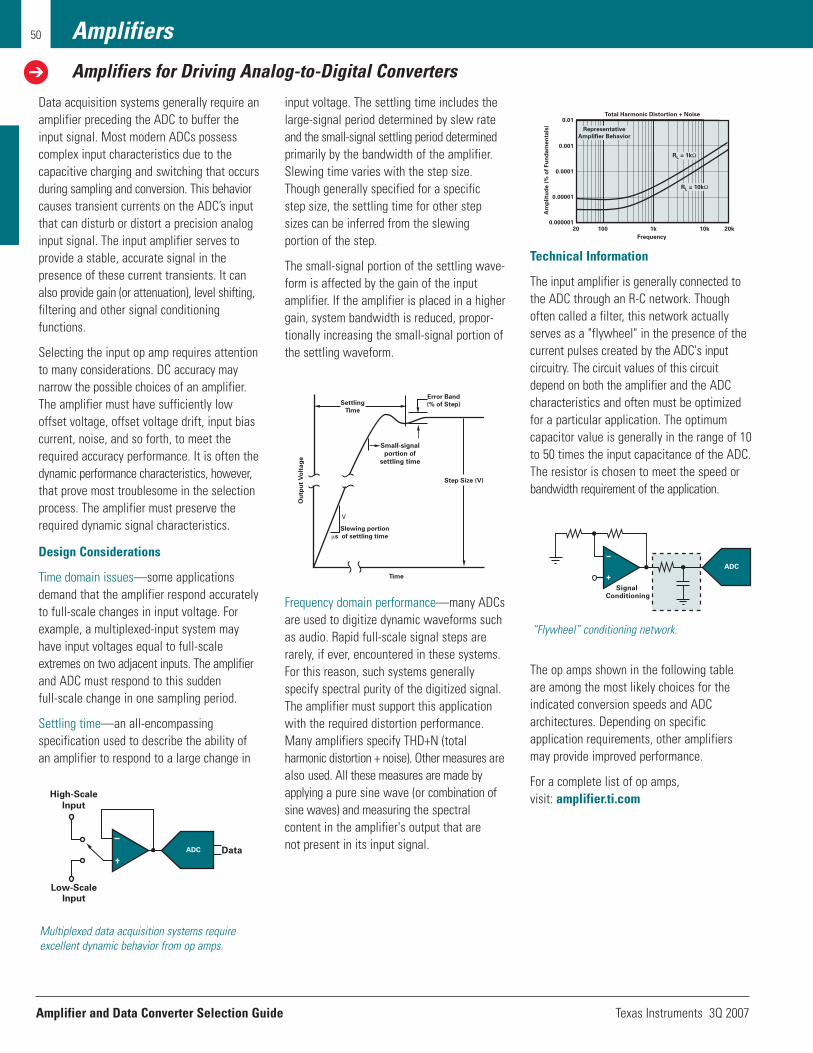
Amplifier and Data Converter Selection Guide Texas Instruments 3Q 2007
50 Amplifiers
Amplifiers for Driving Analog-to-Digital Converters
Data acquisition systems generally require anamplifier preceding the ADC to buffer theinput signal. Most modern ADCs possesscomplex input characteristics due to thecapacitive charging and switching that occurs during sampling and conversion. This behaviorcauses transient currents on the ADC’s inputthat can disturb or distort a precision analoginput signal. The input amplifier serves toprovide a stable, accurate signal in the presence of these current transients. It canalso provide gain (or attenuation), level shifting, filtering and other signal conditioning functions.
Selecting the input op amp requires attentionto many considerations. DC accuracy may narrow the possible choices of an amplifier.The amplifier must have sufficiently low offset voltage, offset voltage drift, input biascurrent, noise, and so forth, to meet therequired accuracy performance. It is often thedynamic performance characteristics, however,that prove most troublesome in the selectionprocess. The amplifier must preserve therequired dynamic signal characteristics.
Design Considerations
Time domain issues—some applicationsdemand that the amplifier respond accuratelyto full-scale changes in input voltage. Forexample, a multiplexed-input system mayhave input voltages equal to full-scaleextremes on two adjacent inputs. The amplifierand ADC must respond to this sudden full-scale change in one sampling period.
Settling time—an all-encompassing specification used to describe the ability ofan amplifier to respond to a large change in
input voltage. The settling time includes thelarge-signal period determined by slew rateand the small-signal settling period determinedprimarily by the bandwidth of the amplifier.Slewing time varies with the step size.Though generally specified for a specific step size, the settling time for other stepsizes can be inferred from the slewing portion of the step.
The small-signal portion of the settling wave-form is affected by the gain of the inputamplifier. If the amplifier is placed in a highergain, system bandwidth is reduced, propor-tionally increasing the small-signal portion ofthe settling waveform.
Frequency domain performance—many ADCsare used to digitize dynamic waveforms suchas audio. Rapid full-scale signal steps arerarely, if ever, encountered in these systems.For this reason, such systems generally specify spectral purity of the digitized signal.The amplifier must support this applicationwith the required distortion performance.Many amplifiers specify THD+N (total harmonic distortion + noise). Other measures arealso used. All these measures are made byapplying a pure sine wave (or combination ofsine waves) and measuring the spectral content in the amplifier's output that are not present in its input signal.
Technical Information
The input amplifier is generally connected tothe ADC through an R-C network. Thoughoften called a filter, this network actuallyserves as a "flywheel" in the presence of thecurrent pulses created by the ADC's input circuitry. The circuit values of this circuitdepend on both the amplifier and the ADCcharacteristics and often must be optimizedfor a particular application. The optimumcapacitor value is generally in the range of 10to 50 times the input capacitance of the ADC.The resistor is chosen to meet the speed orbandwidth requirement of the application.
The op amps shown in the following tableare among the most likely choices for theindicated conversion speeds and ADC architectures. Depending on specific application requirements, other amplifiersmay provide improved performance.
For a complete list of op amps, visit: amplifier.ti.com
ADC
High-Scale
Input
Low-ScaleInput
Data
Multiplexed data acquisition systems requireexcellent dynamic behavior from op amps.
Error Band
(% of Step)Settling
Time
Time
Ou
tpu
t V
olt
ag
e
V
µs
Slewing portion
of settling time
Small-signal
portion of
settling time
Step Size (V)
20
0.001
0.01
0.0001
0.00001
0.000001100 1k
Frequency
Am
pli
tud
e (
% o
f F
un
da
me
nta
ls)
Representative
Amplifier Behavior
RL = 10kΩ
Total Harmonic Distortion + Noise
10k 20k
RL = 1kΩ
Signal Conditioning
ADC
“Flywheel” conditioning network.

Texas Instruments 3Q 2007 Amplifier and Data Converter Selection Guide
Amplifiers
Amplifiers for Driving Analog-to-Digital Converters
51
Amplifiers for ADCs Selection GuideIQ Per Slew VOS Offset VN at
VS VS Ch. GBW Rate (25°C) Drift IB 1kHz Rail-(V) (V) (mA) (MHz) (V/µs) (mV) (µV/°C) (pA) (nV/ Hz) Single to-
Device Description Ch. (min) (max) (max) (typ) (typ) (max) (typ) (max) (typ) Supply Rail Package(s) Price*
For Use with Medium-Speed SAR ADCs (<250kSPS)INA155 Medium Speed, Precision INA 1 2.7 5.5 2.1 0.55 6.5 1 5 10 40 Y Out MSOP $1.10 INA128 High Precision, 120dB CMRR 1 4.5 36 0.75 1.3 4 0.5 0.2 5000 8 N N PDIP, SOIC $3.05 INA331 High Bandwidth, Single Supply 1, 2 2.7 5.5 0.5 5 5 0.5 5 10 46 Y Out MSOP $1.10 OPA340 CMOS, 0.0007% THD+N 1, 2, 4 2.7 5.5 0.95 5.5 6 0.5 2.5 10 25 Y I/O SOT-23, MSOP $0.80 OPA363 1.8V, High CMRR, SHDN 1, 2 1.8 5.5 0.75 7 5 0.5 2 10 17 Y I/O SOT-23, MSOP $0.60 OPA2613 Dual VFB, Low Noise 2 5 12.6 6 12.5 70 1 3.3 12µA 1.8 Y N SOIC, SOIC PowerPAD™ $1.55 OPA211 36V, Bipolar Precision 1,2 5 36 3.6 80 27 0.1 0.2 15000 1.1 Y Out DFN, MSOP, SO8 $3.45OPA627 Ultra-Low THD+N, Wide BW 1 9 36 7.5 16 55 0.1 0.4 5 5.2 N N PDIP, SOIC $12.25 OPA381 Precision High-Speed Amp 1, 2 2.7 5.5 1 18 12 0.025 0.03 50 10 Y Out DFN, MSOP $1.45 OPA228 Precision, Low Noise, G ≥ 5 1, 2, 4 5 36 3.8 33 10 0.075 0.1 10000 3 N N PDIP, SOIC $1.10 OPA350 Precision ADC Driver 1, 2, 4 2.7 5.5 7.5 38 22 0.5 4 10 5 Y I/O PDIP, MSOP $1.30 THS4281 Very Low Power RRIO 1 2.7 15 1 80 35 3.5 4 10 12.5 Y I/O SOT-23, MSOP, SOIC $0.95 OPA2830 Dual, Low Power 1, 2 3 11 3.9 100 500 5.5 — 10,000 9.2 N Out MSOP $0.80THS4032 100MHz, Low Noise 2 5 30 8.5 230 100 2 10 6 1.6 N N MSOP PowerPAD, SOIC $3.35THS4520 Rail-to-Rail Output, FDA1 1 3 5 13 1200 520 2.5 8 11 2 Y Out QFN $2.45 For Use with High-Resolution, Delta-Sigma (∆Σ) ADCsOPA333 1.8V, RRIO, Zero Drift 1,2 1.8 5.5 0.025 0.5 0.16 0.01 0.05 100 — Y I/O SC70, SOT23, SO8 $0.95OPA735 12V, Precision, Auto-Zero Amp 1 2.7 13.2 0.75 1.6 1.5 0.005 0.05 200 — Y Out SOT-23, MSOP $1.25 OPA277 Low Offset and Drift 1, 2, 4 4 36 0.825 1 0.8 0.02 0.1 1000 8 N N QFN, SOIC, PDIP $0.85 OPA227 Ultra-Low Noise, Bipolar Input 1, 2, 4 5 36 3.8 8 2.3 0.075 0.1 10000 3 N N QFN, PDIP, SOIC $1.10 INA326 Auto-Zero INA, 110dB CMRR 1 2.5 5.5 3.4 1kHz — 0.1 0.4 2000 33 Y I/O MSOP $1.80 OPA627 Ultra-Low THD+N, Difet™ 1 9 36 7.5 16 55 0.1 0.4 5 5.2 N N PDIP, SOIC $12.25 OPA336 High Precision, µPower Amp 1, 2, 4 2.3 5.5 0.032 0.1 0.03 0.125 1.5 10 40 Y Out MSOP, PDIP $0.40 INA159 Level Translation Amp 1 1.8 5.5 1.4 1.5 15 0.5 2 — 30 Y I/O MSOP $1.50 INA152 Single-Supply Difference Amp 1 2.7 20 0.65 0.8 0.4 1.5 3 — 87 Y Out MSOP $1.20 For Use with High-Speed SAR (>250kSPS) ADCsOPA2613 Dual VFB, Low Noise 2 5 12.6 6 12.5 70 1 3.3 12µA 1.8 Y N SOIC, SOIC PowerPAD $1.55 OPA727 CMOS, e-trim™, Low Noise 1, 2, 4 4 12 6.5 20 30 0.15 1.5 100 11 Y N MSOP, DFN, TSSOP $1.45 OPAy365 High-Speed, Zero-Crossover, CMOS 1, 2 2.2 5.5 5 50 25 0.5 1 10 100 5 IN SOT23, SO-8 $0.95 OPA358 CMOS, 3V Operation, SC70 1 2.7 3.3 7.5 80 55 6 5 50 6.4 Y Y SC70 $0.45 OPA2830 Dual, Low Power, Wideband, SS 2 3 11 3.9 100 500 1.5 27 10 9.5 Y Out MSOP, SOIC $1.20 THS4130/31 Differential In/Out, SHDN 1 5 30 15 135 52 2 4.5 6µA 1.3 Y N SOIC, MSOP $2.75OPA211 36V, Bipolar Precision 1,2 5 36 3.6 80 27 0.1 0.2 15000 1.1 Y Out DFN, MSOP, SO8 $3.45OPA355 CMOS, 2.7V Operation, SOT23 1, 2, 3 2.7 5.5 11 200 300 9 7 50 5.8 Y Out SOT-23, SOIC $0.90 OPA842 Low Distortion, VFB 1 8 12.6 20.2 200 400 1.2 4 35 2.6 N N SOT-23, SOIC $1.55 THS4032 100MHz, Low Noise 2 5 30 8.5 230 100 2 10 6 1.6 N N MSOP PowerPAD, SOIC $3.35OPA2822 Dual Wideband, Low Noise, VFB 2 4 12.6 4.8 240 170 1.2 5 12µA 2 Y N SOIC, MSOP $1.45 THS4520 Rail-to-Rail Output, FDA1 1 3 5 13 1200 520 2.5 8 11 2 Y Out QFN $2.45 OPA2889 Dual, Low Power, VFB 2 2.6 12 .46 75 250 5 ±20 0.75 8.4 Y N MSOP, SOIC $1.20For Use with High-Speed Data Converters (Pipeline and Flash ADCs)OPA2613 Dual VFB, Low Noise 2 5 12.6 6 12.5 70 1 3.3 12µA 1.8 Y N SOIC $1.55 OPA842 Low Distortion, VFB 1 7 12.6 20.2 200 400 1.2 4 35µA 2.6 Y N SOT-23, SOIC $1.55 OPA847 Low Noise, VFB with SHDN 1 7 12.6 18.1 3900 950 0.5 0.25 39µA 0.85 Y N SOT-23, SOIC $2.00 OPA843 Low Distortion, G ≥ +3, VFB 1 7 12.6 20.2 800 1000 1.2 4 35µA 2 Y N SOT-23, SOIC $1.60 OPA698 Wideband, VFB w/Limiting 1 5 12.6 15.5 250 1100 5 15 10µA 5.6 Y N SOIC $1.90 OPA2690 Dual VFB w/Disable Limiting 2 5 12.6 5.5 300 1800 4.5 12 10µA 5.5 Y N SOIC $2.15 THS4502/03 Differential In/Out, SHDN 1 4.5 15 28 370 2800 –4/+2 10 4.6µA 6.8 Y N MSOP $4.00 OPA695 Ultra-Wideband CFB 1 5 12.6 12.3 — 4300 3 10 37µA 1.8 Y N SOT-23, SOIC $1.35 THS4511 Wideband, Low Noise, FDA1 1 3 5 39.2 2000 4900 5.2 2.6 15.5µA 2 Y N QFN $3.45 THS4513 Wideband, Low Noise, FDA1 1 3 5 37.7 2000 5100 5.2 2.6 13µA 2.2 Y N QFN $3.25 THS4508 Wideband, FDA1 1 3 5 39.2 3000 6400 5 2.6 15.5µA 2.3 Y N QFN $3.95 THS4509 Low Distortion, FDA1 1 3 5 37.7 3000 6600 0.8 2.6 13µA 1.9 Y N QFN $3.75THS4520 Rail-to-Rail Output, FDA1 1 3 5 13 1200 520 2.5 8 11 2 Y Out QFN $2.45 1Fully differential amplifier * Suggested resale price in U.S. dollars in quantities of 1,000. New products are listed in bold red. Preview products are listed in bold blue.

Amplifier and Data Converter Selection Guide Texas Instruments 3Q 2007
52 ADCs by Architecture
Delta-Sigma (∆Σ) ADCs
Delta-sigma converters are capable of veryhigh resolution, and are ideal for convertingsignals over a very wide range of frequenciesfrom DC to several megahertz. In a delta-sigma ADC, the input signal is oversampled bya modulator, then filtered and decimated by adigital filter producing a high-resolution datastream at a lower sampling rate.
The delta-sigma architecture approachallows resolution to be traded for speed andboth to be traded for power. This nearly continuous relationship between data rate,resolution and power consumption makesdelta-sigma converters extraordinarily flexible.In many delta-sigma converters, this relationship is programmable, allowing a single device to handle multiple measurement requirements.
Because delta-sigma converters oversampletheir inputs, they can perform most anti-aliasing filtering in the digital domain.Modern VLSI design techniques havebrought the cost of complex digital filters farbelow the cost of their analog equivalents.Formerly unusual functions, such as simultaneous 50Hz and 60Hz notch filtering,are now built into many delta-sigma ADCs.
Typical high-resolution applications for delta-sigma ADCs include audio, industrialprocess control, analytical and test instrumentation and medical instrumentation.
Recent innovations in ADC architectureshave led to a new class of ADC architecturewhich uses both the pipeline and the oversampling principle.These, very high-speedconverters push the data rates into the MSPSrange, while maintaining resolutions of 16-bits and higher.These speeds enable ahost of new wide bandwidth signal processingapplications such as communications andmedical imaging.
Most delta-sigma ADCs have inherently differential inputs. They measure the actualdifference between two voltages, instead ofthe difference between one voltage andground. The differential input structure of adelta-sigma makes it ideal for measuring
differential sources such as bridge sensorsand thermocouples. Frequently, no inputamplifiers are required for these applications.
Delta-sigma converters work differently thanSAR converters. A SAR takes a "snapshot" ofan input voltage and analyzes it to determinethe corresponding digital code. A delta-sigmameasures the input signal for a certain period of time and outputs a digital code corresponding to the signal's average overthat time. It is important to remember theway delta-sigma converters operate, particularly for designs incorporating multiplexing and synchronization.
It is very easy to synchronize delta-sigmaconverters together, so that they sample atthe same time but it's more difficult to synchronize a delta-sigma converter to anexternal event. Delta-sigma converters arehighly resistant to system clock jitter. Theaction of oversampling effectively averagesthe jitter, reducing its impact on noise.
Many delta-sigma converters include inputbuffers and programmable gain amplifiers(PGA). An input buffer increases the inputimpedance to allow direct connection to highsource impedance signals. A PGA increasesthe converter’s resolution when measuringsmall signals. Bridge sensors are an exampleof a signal source that can take advantage ofthe PGA within the converter.
Every ADC requires a reference, and for high-resolution converters, low-noise, low-drift references are critical. Most delta-sigma converters have differential reference inputs.
The following pages provide a broad rangeof delta-sigma ADCs available from TI for a wide range of applications.
To help facilitate the selection process, an interactive online data converter parametric search engine is available at dataconverter.ti.com with links to all data converter specifications.
Analog Input
DigitalOutput
DifferentialAmplifier
Integrator
Comparator
Modulator
DigitalFilter
DAC
Delta-sigma ADCs consist of a delta-sigma modulator followed by a digital decimation filter. The modulator incorporates a comparator and integrator in afeedback loop with a DAC. The loop is synchronized by a clock.
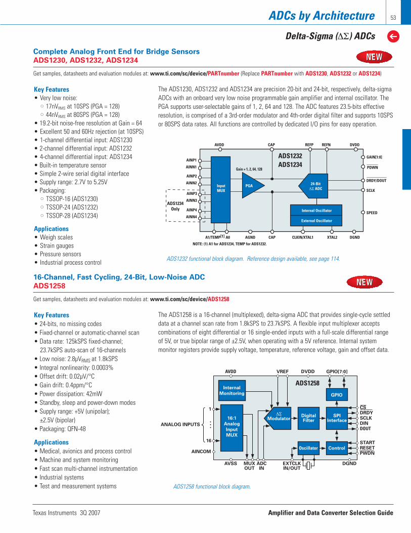
Texas Instruments 3Q 2007 Amplifier and Data Converter Selection Guide
ADCs by Architecture
Delta-Sigma (∆Σ) ADCs
53
A1/TEMP[1] A0 AGND
AVDD
GAIN[1:0]
PDWN
DRDY/DOUT
Internal Oscillator
External Oscillator
SCLK
SPEED
CAP
CAP CLKIN/XTAL1 XTAL2 DGND
Gain = 1, 2, 64, 128
REFP REFN DVDD
ADS1234Only
InputMUX
24-Bit∆Σ ADC
NOTE: (1) A1 for ADS1234, TEMP for ADS1232.
PGA
AINP4
AINN4
AINP1
AINN1
AINP2
AINN2
AINP3
AINN3
Complete Analog Front End for Bridge Sensors
ADS1230, ADS1232, ADS1234
Get samples, datasheets and evaluation modules at: www.ti.com/sc/device/PARTnumber (Replace PARTnumber with ADS1230, ADS1232 or ADS1234)
ADS1232 functional block diagram. Reference design available, see page 114.
Key Features• Very low noise:
•• 17nVRMS at 10SPS (PGA = 128)•• 44nVRMS at 80SPS (PGA = 128)
• 19.2-bit noise-free resolution at Gain = 64• Excellent 50 and 60Hz rejection (at 10SPS)• 1-channel differential input: ADS1230• 2-channel differential input: ADS1232 • 4-channel differential input: ADS1234• Built-in temperature sensor• Simple 2-wire serial digital interface• Supply range: 2.7V to 5.25V• Packaging:
•• TSSOP-16 (ADS1230)•• TSSOP-24 (ADS1232)•• TSSOP-28 (ADS1234)
Applications• Weigh scales• Strain gauges• Pressure sensors• Industrial process control
The ADS1230, ADS1232 and ADS1234 are precision 20-bit and 24-bit, respectively, delta-sigmaADCs with an onboard very low noise programmable gain amplifier and internal oscillator. ThePGA supports user-selectable gains of 1, 2, 64 and 128. The ADC features 23.5-bits effectiveresolution, is comprised of a 3rd-order modulator and 4th-order digital filter and supports 10SPSor 80SPS data rates. All functions are controlled by dedicated I/O pins for easy operation.
∆ΣModulator
DigitalFilter
Internal
Monitoring
16:1
Analog
Input
MUX
1
16
AINCOM
…
ADCIN
EXTCLKIN/OUT
AVSS DGND
AVDD DVDD
MUXOUT
SPIInterface
CSDRDYSCLKDINDOUT
ControlOscillator
GPIO
STARTRESETPWDN
GPIO[7:0]VREF
ANALOG INPUTS
16-Channel, Fast Cycling, 24-Bit, Low-Noise ADC
ADS1258
Get samples, datasheets and evaluation modules at: www.ti.com/sc/device/ADS1258
Key Features• 24-bits, no missing codes• Fixed-channel or automatic-channel scan• Data rate: 125kSPS fixed-channel;
23.7kSPS auto-scan of 16-channels• Low noise: 2.8µVRMS at 1.8kSPS• Integral nonlinearity: 0.0003%• Offset drift: 0.02µV/°C• Gain drift: 0.4ppm/°C• Power dissipation: 42mW• Standby, sleep and power-down modes• Supply range: +5V (unipolar);
±2.5V (bipolar)• Packaging: QFN-48
Applications• Medical, avionics and process control• Machine and system monitoring• Fast scan multi-channel instrumentation• Industrial systems• Test and measurement systems
The ADS1258 is a 16-channel (multiplexed), delta-sigma ADC that provides single-cycle settleddata at a channel scan rate from 1.8kSPS to 23.7kSPS. A flexible input multiplexer acceptscombinations of eight differential or 16 single-ended inputs with a full-scale differential rangeof 5V, or true bipolar range of ±2.5V, when operating with a 5V reference. Internal system monitor registers provide supply voltage, temperature, reference voltage, gain and offset data.
ADS1258 functional block diagram.
ADS1232ADS1234
ADS1258

Amplifier and Data Converter Selection Guide Texas Instruments 3Q 2007
ADCs by Architecture
Delta-Sigma (∆Σ) ADCs
54
VREFP VREFN AVDD DVDD
SYNC/PDWN
MODE
CLK
DRDY/FSYNC
SCLK
DOUT
DIN
FORMAT
DGNDAGND
AINN
AINP
Modulator
DigitalFilter
SerialInterface
ControlLogic
∆Σ
24-Bit ADC with DC Accuracy and AC PerformanceADS1271, ADS1274*, ADS1278*
Get samples, datasheets and evaluation modules at: www.ti.com/sc/device/PARTnumber (Replace PARTnumber with ADS1271, ADS1274 or ADS1278)
Traditionally, industrial delta-sigma ADCs offering good drift performance used digital filters with largepassband droop. As a result, they have limited signal bandwidth and are mostly suited for DC measure-ments. High-resolution ADCs in audio applications offer larger usable bandwidths, but the offset and driftspecification are significantly weaker than their industrial counterparts. The ADS1271, ADS1274 andADS1278 combine these converter types, allowing high-precision industrial measurement with excellentDC and AC specifications ensured over an extended industrial temperature range.
*ADS1274 and ADS1278 expected release date 4Q 07.
Key Features• AC performance:
•• Bandwidth: 51kHz •• THD: –105dB
• DC accuracy:•• Offset drift: 1.8µV/°C •• Gain drift: 2ppm/°C
• Selectable operating modes:•• High speed: 105kSPS data rate•• High resolution: 109dB SNR•• Low power: 35mW dissipation
• Selectable SPI or frame sync serial interface
• Designed for multichannel systems• Analog supply: 5V• Digital supply: 1.8V to 3.3V• Packaging: TSSOP-16
Applications• Vibration/modal analysis• Acoustics• Dynamic strain gauges• Pressure sensors• Test and measurement
The ADS1271 is a single-channel, 24-bit, delta-sigma ADC with up to 105kSPS data rate. TheADS1274 (quad) and ADS1278 (octal) ADCs offer simultaneous sampling rates up to 125kSPS(max) and all offer a unique combination of excellent DC accuracy and outstanding AC performance. The high-order, chopper-stabilized modulator achieves very low drift with low in-band noise. The onboard decimation filter suppresses modulator and out-of-band noise.
ADS1271 functional block diagram.
ADS1271
MUX
TEMPEN VREFP VREFN
BufferADC
Serial
Interface
Oscillator
AIN P1
AIN N1
AIN P2
AIN N2
AIN P
AIN N
BUFEN
VREF
VIN
MUX
MODE
START
SCLK
DRDY/DOUT
24-Bit, One- and Two-Channel Differential Input ADCs with Internal OscillatorADS1225, ADS1226
Get samples, datasheets and evaluation modules at: www.ti.com/sc/device/ADS1225 and www.ti.com/sc/device/ADS1226
Key Features• Data rate: 100SPS (high-speed mode)• Easy control with dedicated start pin• Single-cycle settling• Low noise: 4µVRMS (high-resolution mode)• Low power: 1mW operation; <1µA shutdown• Self-calibrating• Simple read-only, 2-wire serial interface• Internal temperature sensor• Internal oscillator• Analog and digital supplies: 2.7V to 5.5V• Packaging: QFN-16
Applications• Hand-held instruments• Portable medical equipment• Industrial process control
The ADS1225 (single channel) and ADS1226 (dual channel) are 24-bit delta-sigma ADCs that converton command using a dedicated START pin. Simply pulse this pin to initiate a conversion. Data is readin a single cycle for retrieval over a 2-wire serial interface that easily connects to popular micro-controllers like TI’s MSP430. After conversion, the device shuts down. Features include a two-channel multiplexer (ADS1226), selectable input buffer, temp sensor, oscillator and two operatingmodes allow optimization for speed or resolution.
ADS1225 and ADS1226 functional block diagram.
ADS1225
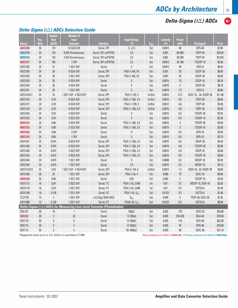
Texas Instruments 3Q 2007 Amplifier and Data Converter Selection Guide
ADCs by Architecture
Delta-Sigma (∆Σ) ADCs
55
Delta-Sigma (∆Σ) ADCs Selection GuideSample Number of
Res. Rate Input Input Voltage Linearity PowerDevice (Bits) (kSPS) Channels Interface (V) VREF (%) (mW) Package(s) Price*
ADS1258 24 125 16 SE/8 Diff Serial, SPI 5, ±2.5 Ext 0.0015 40 QFN-48 $7.95 ADS1278 24 125 8 Diff Simultaneous Serial, SPI w/FSYNC 2.5 Ext 0.001 60-600 TQFP-64 $23.95ADS1274 24 125 4 Diff Simultaneous Serial, SPI w/FSYNC 2.5 Ext 0.001 30-300 TQFP-64 $13.95ADS1271 24 105 1 Diff Serial, SPI w/FSYNC 2.5 Ext 0.0015 35-100 TSSOP-16 $5.90 ADS1252 24 41 1 SE/1 Diff Serial 5 Ext 0.0015 40 SOIC-8 $6.45ADS1256 24 30 8 SE/4 Diff Serial, SPI PGA (1-64), 5V Ext 0.001 35 SSOP-28 $6.95 ADS1255 24 30 2 SE/1 Diff Serial, SPI PGA (1-64), 5V Ext 0.001 35 SSOP-20 $6.50 ADS1253 24 20 4 SE/4 Diff Serial 5 Ext 0.0015 7.5 SSOP-16 $6.70 ADS1254 24 20 4 SE/4 Diff Serial 5 Ext 0.0015 4 SSOP-20 $6.70 ADS1251 24 20 1 SE/1 Diff Serial 5 Ext 0.0015 7.5 SOIC-8 $5.60 ADS1210/11 24 16 1 SE/1 Diff 4 SE/4 Diff Serial, SPI PGA (1-16), 5 Int/Ext 0.0015 27.5 SOIC-18 , -24, SSOP-28 $11.00 ADS1216 24 0.78 8 SE/4 Diff Serial, SPI PGA (1-128), 2.5 Int/Ext 0.0015 0.6 TQFP-48 $5.00 ADS1217 24 0.78 8 SE/4 Diff Serial, SPI PGA (1-128), 5 Int/Ext 0.0012 0.8 TQFP-48 $5.00 ADS1218 24 0.78 8 SE/4 Diff Serial, SPI PGA (1-128), 2.5 Int/Ext 0.0015 0.8 TQFP-48 $5.50 ADS1224 24 0.24 4 SE/4 Diff Serial 5 Ext 0.0015 0.5 TSSOP-20 $3.25 ADS1222 24 0.24 2 SE/2 Diff Serial 5 Ext 0.0015 0.5 TSSOP-14 $2.95 ADS1234 24 0.08 4 SE/4 Diff Serial PGA (1-128), 2.5 Ext 0.0015 3 TSSOP-28 $4.50 ADS1232 24 0.08 2 SE/2 Diff Serial PGA (1-128), 2.5 Ext 0.0015 3 TSSOP-24 $3.90 ADS1226 24 0.08 2 Diff Serial 5 Ext 0.0015 0.5 QFN-16 $2.95 ADS1225 24 0.08 1 Diff Serial 5 Ext 0.0015 0.5 QFN-16 $2.75 ADS1241 24 0.015 8 SE/4 Diff Serial, SPI PGA (1-128), 2.5 Ext 0.0015 0.5 SSOP-28 $4.20 ADS1243 24 0.015 8 SE/4 Diff Serial, SPI PGA (1-128), 2.5 Ext 0.0015 0.6 TSSOP-20 $3.95 ADS1240 24 0.015 4 SE/2 Diff Serial, SPI PGA (1-128), 2.5 Ext 0.0015 0.6 SSOP-24 $3.80 ADS1242 24 0.015 4 SE/2 Diff Serial, SPI PGA (1-128), 2.5 Ext 0.0015 0.6 TSSOP-16 $3.60 ADS1244 24 0.015 1 SE/1 Diff Serial 5 Ext 0.0008 0.3 MSOP-10 $2.95 ADS1245 24 0.015 1 SE/1 Diff Serial 2.5 Ext 0.0015 0.5 MSOP-10 $3.10 ADS1212/13 22 6.25 1 SE/1 Diff 4 SE/4 Diff Serial, SPI PGA (1-16), 5 Int/Ext 0.0015 1.4 SOIC-18, -24, SSOP-28 $9.00 ADS1250 20 25 1 SE/1 Diff Serial, SPI PGA (1-8), 4 Ext 0.003 75 SOIC-16 $6.95 ADS1230 20 0.08 1 SE/1 Diff Serial 0.02 Ext 0.003 3 TSSOP-16 $2.50 ADS1112 16 0.24 3 SE/2 Diff Serial, I2C PGA (1-8), 2.048 Int 0.01 0.7 MSOP-10, SON-10 $2.65 ADS1110 16 0.24 1 SE/1 Diff Serial, I2C PGA (1-8), 2.048 Int 0.01 0.7 SOT23-6 $1.95 ADS1100 16 0.128 1 SE/1 Diff Serial, I2C PGA (1-8), VDD Ext 0.0125 0.3 SOT23-6 $1.80 TLC7135 14 3 1 SE/1 Diff ±4.5 Digit MUX BCD VREF Ext 0.005 5 PDIP-28, SOIC-28 $1.95 ADS1000 12 0.128 1 SE/1 Diff Serial, I2C PGA(1-8), VDD Ext 0.0125 0.3 SOT23-6 $0.99 Delta-Sigma (∆Σ) ADCs for Measuring Low-Level Currents (Photodiodes)DDC101 20 10 1 Serial 500pC Ext 0.025 170 SOIC-24 $29.00 DDC232 20 3 32 Serial 12-350pC Ext 0.025 224-320 BGA-64 $70.00 DDC118 20 3 8 Serial 12-350pC Ext 0.025 110 QFN-48 $32.00 DDC114 20 3 4 Serial 12-350pC Ext 0.025 55 QFN-48 $18.00 DDC112 20 3 2 Serial 50-1000pC Ext 0.025 80 SOIC-28 $12.10
*Suggested resale price in U.S. dollars in quantities of 1,000. New products are listed in bold red. Preview products are listed in bold blue.

Amplifier and Data Converter Selection Guide Texas Instruments 3Q 2007
56 ADCs by Architecture
Wide Bandwidth ∆Σ ADCs
TI’s wide bandwidth Delta-Sigma (∆Σ) ADCsare capable of very high resolution and arecapable of converting signals over a very widerange of frequencies from DC to severalmegahertz. Systems using these ADCs benefitfrom high speed, precision performance, andwide bandwidth (DC to 5MHz).
These ADCs employ a multi-stage propriatary-modulator architecture, which offer the advan-tage of inherent stability, and higher SQNRwith lower oversampling ratio (OSR).Furthermore, these high-speed, ∆Σ convertersare highly resistant to system clock jitter. Theaction of oversampling effectively averages thejitter, reducing the impact on noise.
The combination of speed and precisionenable wide bandwidth signal processingapplications for advanced scientific instrumen-tation for biomedical, bench test and measure,and communications applications.
PD
SYNC
CLK
CS
2X MODE
RD
DRDY
OTR
DOUT[15:0]
AVDD DVDD
Modulator
Bias Circuits
DigitalFilter
ParallelInterface
AGND DGND
AINP
AINN
VREFP VREFN VMID RBIAS VCAP
16-Bit, 10MSPS, Very Wide Bandwidth ADC
ADS1610
Get samples, datasheets, evaluation modules and app reports at: www.ti.com/sc/device/ADS1610
Key Features• Output data rate: 10MSPS• Signal bandwidth: 4.9MHz• SNR: 86dBFS• THD: –94dB• SFDR: 95dB• SYNC pin for simultaneous sampling with
multiple ADS1610s• Group delay: 3µs• Pin-compatible with ADS1605
(5MSPS ADC)• Packaging: TQFP-64
Applications• Scientific instruments• Test equipment• Communications• Wide-band signal analysis
The ADS1610 is a 10MSPS, high-precision ∆Σ ADC operating from a +5V analog and a +3V digital supply. Featuring an advanced multi-stage analog modulator combined with on-chip digital decimation filter, the ADS1610 achieves 86dBFS SNR at a 4.9MHz signal bandwidth.Output data is supplied over a parallel interface and easily connects to TMS320™ DSPs. Powerdissipation can be adjusted with an external resistor, allowing for reduction at lower operatingspeeds.
ADS1610 functional block diagram.
ADS1610
Delta-Sigma (∆Σ) ADCs Selection GuideSample Number of Signal
Res. Rate Input Bandwidth SNR THD PowerDevice (Bits) (kSPS) Channels Interface (kHz) (dB) (dB) (mW) Package Price*
Wide Bandwidth Delta-Sigma (∆Σ) ADCsADS1626 18 1250 1 Diff P18 w/FIFO 615 93 –101 515 TQFP-64 $15.50ADS1625 18 1250 1 Diff P18 615 93 –101 515 TQFP-64 $14.95ADS1610 16 10000 1 Diff P16 4900 86 –94 960 TQFP-64 $19.95 ADS1606 16 5000 1 Diff P16 w/FIFO 2450 88 –99 570 TQFP-64 $15.50ADS1605 16 5000 1 Diff P16 2450 88 –99 570 TQFP-64 $14.95ADS1602 16 2500 1 Diff Serial 1230 91 –103 530 TQFP-48 $12.50ADS1601 16 1250 1 Diff Serial 615 92 –103 350 TQFP-48 $9.95
*Suggested resale price in U.S. dollars in quantities of 1,000. New products are listed in bold red.
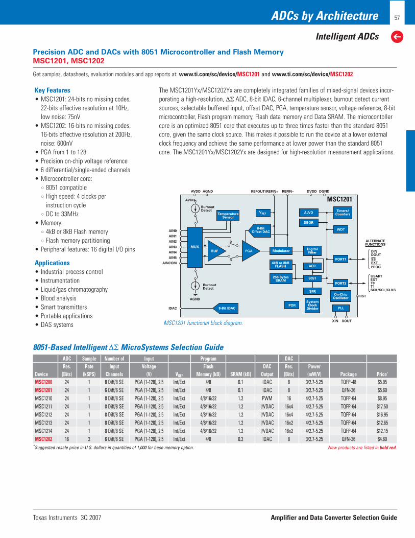
Texas Instruments 3Q 2007 Amplifier and Data Converter Selection Guide
ADCs by Architecture
Intelligent ADCs
57
AVDD AGND
AVDD
BurnoutDetect
AIN0
AIN1
AIN2
AIN3
AIN4
AIN5
AINCOM
MUX
TemperatureSensor
BUF
BurnoutDetect
AGND
8-Bit IDACPOR
SystemClock
Divider
SFR
256 BytesSRAM
8051
ACC
DigitalFilter
ModulatorPGA
4kB or 8kBFLASH
8-BitOffset DAC
VREF
PLL
On-ChipOscillator
PORT3
PORT1
WDT
ALVD
DBOR
Timers/Counters
REFOUT/REFIN+ REFIN– DVDD DGND
ALTERNATEFUNCTIONS
DINDOUT
SSEXT
PROG
USARTEXTT0T1SCK/SCL/CLKS
RST
XIN XOUT
IDAC
Precision ADC and DACs with 8051 Microcontroller and Flash Memory
MSC1201, MSC1202
Get samples, datasheets, evaluation modules and app reports at: www.ti.com/sc/device/MSC1201 and www.ti.com/sc/device/MSC1202
MSC1201 functional block diagram.
The MSC1201Yx/MSC1202Yx are completely integrated families of mixed-signal devices incor-porating a high-resolution, ∆Σ ADC, 8-bit IDAC, 6-channel multiplexer, burnout detect currentsources, selectable buffered input, offset DAC, PGA, temperature sensor, voltage reference, 8-bitmicrocontroller, Flash program memory, Flash data memory and Data SRAM. The microcontollercore is an optimized 8051 core that executes up to three times faster than the standard 8051core, given the same clock source. This makes it possible to run the device at a lower externalclock frequency and achieve the same performance at lower power than the standard 8051core. The MSC1201Yx/MSC1202Yx are designed for high-resolution measurement applications.
8051-Based Intelligent ∆Σ MicroSystems Selection GuideADC Sample Number of Input Program DACRes. Rate Input Voltage Flash DAC Res. Power
Device (Bits) (kSPS) Channels (V) VREF Memory (kB) SRAM (kB) Output (Bits) (mW/V) Package Price*
MSC1200 24 1 8 Diff/8 SE PGA (1-128), 2.5 Int/Ext 4/8 0.1 IDAC 8 3/2.7-5.25 TQFP-48 $5.95 MSC1201 24 1 6 Diff/6 SE PGA (1-128), 2.5 Int/Ext 4/8 0.1 IDAC 8 3/2.7-5.25 QFN-36 $5.60 MSC1210 24 1 8 Diff/8 SE PGA (1-128), 2.5 Int/Ext 4/8/16/32 1.2 PWM 16 4/2.7-5.25 TQFP-64 $8.95 MSC1211 24 1 8 Diff/8 SE PGA (1-128), 2.5 Int/Ext 4/8/16/32 1.2 I/VDAC 16x4 4/2.7-5.25 TQFP-64 $17.50 MSC1212 24 1 8 Diff/8 SE PGA (1-128), 2.5 Int/Ext 4/8/16/32 1.2 I/VDAC 16x4 4/2.7-5.25 TQFP-64 $16.95 MSC1213 24 1 8 Diff/8 SE PGA (1-128), 2.5 Int/Ext 4/8/16/32 1.2 I/VDAC 16x2 4/2.7-5.25 TQFP-64 $12.65 MSC1214 24 1 8 Diff/8 SE PGA (1-128), 2.5 Int/Ext 4/8/16/32 1.2 I/VDAC 16x2 4/2.7-5.25 TQFP-64 $12.15 MSC1202 16 2 6 Diff/6 SE PGA (1-128), 2.5 Int/Ext 4/8 0.2 IDAC 8 3/2.7-5.25 QFN-36 $4.60
*Suggested resale price in U.S. dollars in quantities of 1,000 for base memory option. New products are listed in bold red.
Key Features• MSC1201: 24-bits no missing codes,
22-bits effective resolution at 10Hz,low noise: 75nV
• MSC1202: 16-bits no missing codes,16-bits effective resolution at 200Hz,noise: 600nV
• PGA from 1 to 128• Precision on-chip voltage reference• 6 differential/single-ended channels• Microcontroller core:
•• 8051 compatible•• High speed: 4 clocks per
instruction cycle•• DC to 33MHz
• Memory:•• 4kB or 8kB Flash memory•• Flash memory partitioning
• Peripheral features: 16 digital I/O pins
Applications• Industrial process control• Instrumentation• Liquid/gas chromatography• Blood analysis• Smart transmitters• Portable applications• DAS systems
MSC1201

Amplifier and Data Converter Selection Guide Texas Instruments 3Q 2007
58 ADCs by Architecture
SAR ADCs
Successive-approximation register (SAR) converters are frequently the architecture ofchoice for medium-to-high-resolution applications with medium sampling rates.SAR ADCs range in resolution from 8- to 18-bits with speeds typically less than10MSPS. They provide low power consumption and a small form factor.
A SAR converter operates on the same principleas a balance scale. On the scale, an unknownweight is placed on one side of the balancepoint, while known weights are placed on theother side and rejected or kept until the twosides are perfectly balanced. The unknownweight can then be measured by totaling upthe kept, known weights. In the SAR converter,the input signal is the unknown weight, whichis sampled and held. This voltage is then compared to successive known voltages, andthe results are output by the converter. Unlikethe weigh scale, conversion occurs very quickly through the use of charge redistributiontechniques.
Because the SAR ADC samples the input signaland holds the sampled value until conversion iscomplete, this architecture does not make anyassumptions about the nature of the input signal, and the signal therefore does not needto be continuous. This makes the SAR architecture ideal for applications where amultiplexer may be used prior to the converter, or for applications where the converter may only need to make a measurement once every few seconds, or forapplications where a “fast” measurement isrequired. The conversion time remains thesame in all cases, and has little sample-to-conversion latency compared to a pipeline ordelta-sigma converter. SAR converters areideal for real-time applications such asindustrial control, motor control, power management, portable/battery-poweredinstruments, PDAs, test equipment anddata/signal acquisition.
Technical Information
Modern SAR ADCs use a sample capacitorthat is charged to the voltage of the inputsignal. Due to the ADC's input capacitance,input impedance, and external circuitry, a settling time will be required for the samplecapacitor's voltage to match the measuredinput voltage.
Minimizing the external circuitry's sourceimpedance is one way to minimize this settling time, assuring that the input signal isaccurately acquired within the ADC’s acquisitiontime. A more troublesome design constraint,however, is the dynamic load that the SARADC's input presents to the driving circuitry.The op amp driver to the ADC input must beable to handle this dynamic load and settleto the desired accuracy within the requiredacquisition time.
The SAR ADC's reference input circuitry presentsa similar load to the reference voltage. Whilethe reference voltage is supposed to be a verystable DC voltage, the dynamic load that theADC's reference input presents makes achieving
this goal somewhat difficult. Thus, buffer circuitry is required for the reference voltage, and the op amp used for this hassimilar requirements as that used for drivingthe ADC input; in fact, the requirements onthe op amp may be even higher than for theinput signal as the reference input must be settled within one clock cycle. Some convertershave this reference buffer amplifier built in.
Buffering these inputs using op amps with alow, wideband output impedance is the bestway to preserve accuracy with these converters.
To help facilitate the selection process, an interactive online data converter parametric search engine is available at dataconverter.ti.com with links to all data converter specifications.
SAR
Se
ria
l In
terf
ace
CDAC
REF
SERIAL
DCLO
CS/SH
In a SAR ADC, the bits are decided by a single high-speed, high-accuracy comparator bit by bit, from the MSB down to the LSB. This is done by comparing the analog input with a DAC whose output is updated by previously decided bits and successively approximates the analog input.
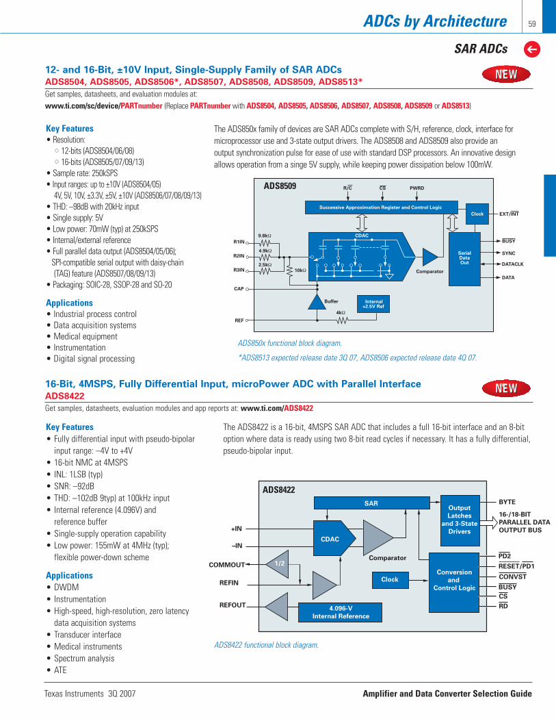
Texas Instruments 3Q 2007 Amplifier and Data Converter Selection Guide
ADCs by Architecture
SAR ADCs
59
16-Bit, 4MSPS, Fully Differential Input, microPower ADC with Parallel Interface
ADS8422
Get samples, datasheets, evaluation modules and app reports at: www.ti.com/ADS8422
Key Features• Fully differential input with pseudo-bipolar
input range: –4V to +4V• 16-bit NMC at 4MSPS• INL: 1LSB (typ)• SNR: –92dB• THD: –102dB 9typ) at 100kHz input• Internal reference (4.096V) and
reference buffer• Single-supply operation capability• Low power: 155mW at 4MHz (typ);
flexible power-down scheme
Applications• DWDM• Instrumentation• High-speed, high-resolution, zero latency
data acquisition systems• Transducer interface• Medical instruments• Spectrum analysis• ATE
The ADS8422 is a 16-bit, 4MSPS SAR ADC that includes a full 16-bit interface and an 8-bitoption where data is ready using two 8-bit read cycles if necessary. It has a fully differential,pseudo-bipolar input.
ADS8422 functional block diagram.
+IN
–IN
COMMOUT
REFIN
REFOUT
1/2
4.096-V
Internal Reference
Clock
CDAC
SAR
Comparator
Output
Latches
and 3-State
Drivers
Conversion
and
Control Logic
BYTE
16-/18-BIT
PARALLEL DATA
OUTPUT BUS
PD2
RESET/PD1
CONVST
BUSY
CS
RD
Successive Approximation Register and Control Logic
R/C CS PWRD
Clock EXT/INT
BUSY
SYNC
DATA
SerialDataOut
Comparator
CDAC9.8kΩ
4.9kΩ
2.5kΩ
R1IN
R2IN
R3IN
CAP
REF
Buffer
10kΩ
4kΩ
Internal+2.5V Ref
DATACLK
12- and 16-Bit, ±10V Input, Single-Supply Family of SAR ADCs
ADS8504, ADS8505, ADS8506*, ADS8507, ADS8508, ADS8509, ADS8513*
Get samples, datasheets, and evaluation modules at: www.ti.com/sc/device/PARTnumber (Replace PARTnumber with ADS8504, ADS8505, ADS8506, ADS8507, ADS8508, ADS8509 or ADS8513)
ADS850x functional block diagram.
*ADS8513 expected release date 3Q 07, ADS8506 expected release date 4Q 07.
Key Features• Resolution:
•• 12-bits (ADS8504/06/08)•• 16-bits (ADS8505/07/09/13)
• Sample rate: 250kSPS• Input ranges: up to ±10V (ADS8504/05)
4V, 5V, 10V, ±3.3V, ±5V, ±10V (ADS8506/07/08/09/13)• THD: –98dB with 20kHz input• Single supply: 5V• Low power: 70mW (typ) at 250kSPS• Internal/external reference• Full parallel data output (ADS8504/05/06);
SPI-compatible serial output with daisy-chain (TAG) feature (ADS8507/08/09/13)
• Packaging: SOIC-28, SSOP-28 and SO-20
Applications• Industrial process control• Data acquisition systems• Medical equipment• Instrumentation• Digital signal processing
The ADS850x family of devices are SAR ADCs complete with S/H, reference, clock, interface for microprocessor use and 3-state output drivers. The ADS8508 and ADS8509 also provide an output synchronization pulse for ease of use with standard DSP processors. An innovative designallows operation from a singe 5V supply, while keeping power dissipation below 100mW.
ADS8422
ADS8509
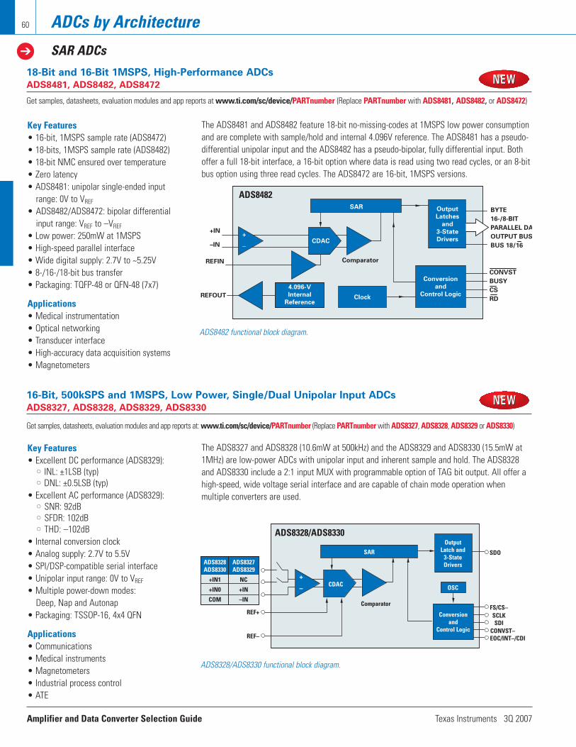
Amplifier and Data Converter Selection Guide Texas Instruments 3Q 2007
ADCs by Architecture
SAR ADCs
60
SAR Output
Latches
and
3-State
Drivers
BYTE
16-/8-BIT
PARALLEL DA
OUTPUT BUS
BUS 18/16
CONVST
BUSY
CS
RD
Conversion
and
Control LogicClockREFOUT
Comparator
+IN
–IN
REFIN
4.096-V
Internal
Reference
+CDAC
18-Bit and 16-Bit 1MSPS, High-Performance ADCs
ADS8481, ADS8482, ADS8472
Get samples, datasheets, evaluation modules and app reports at www.ti.com/sc/device/PARTnumber (Replace PARTnumber with ADS8481, ADS8482, or ADS8472)
ADS8482 functional block diagram.
Key Features• 16-bit, 1MSPS sample rate (ADS8472)• 18-bits, 1MSPS sample rate (ADS8482)• 18-bit NMC ensured over temperature• Zero latency• ADS8481: unipolar single-ended input
range: 0V to VREF
• ADS8482/ADS8472: bipolar differential input range: VREF to –VREF
• Low power: 250mW at 1MSPS• High-speed parallel interface• Wide digital supply: 2.7V to ~5.25V• 8-/16-/18-bit bus transfer• Packaging: TQFP-48 or QFN-48 (7x7)
Applications• Medical instrumentation• Optical networking• Transducer interface• High-accuracy data acquisition systems• Magnetometers
The ADS8481 and ADS8482 feature 18-bit no-missing-codes at 1MSPS low power consumptionand are complete with sample/hold and internal 4.096V reference. The ADS8481 has a pseudo-differential unipolar input and the ADS8482 has a pseudo-bipolar, fully differential input. Bothoffer a full 18-bit interface, a 16-bit option where data is read using two read cycles, or an 8-bitbus option using three read cycles. The ADS8472 are 16-bit, 1MSPS versions.
C O N V E R S IO N&
C O N T R O LL O G IC
REF+
REF–
SAR
ADS8328ADS8330
+IN1
+IN0
COM
ADS8327ADS8329
NC
+IN
–IN
SDO
FS/CS–SCLK SDI
CONVST–EOC/INT–/CDI
Comparator
CDAC
OutputLatch and
3-StateDrivers
OSC
Conversionand
Control Logic
16-Bit, 500kSPS and 1MSPS, Low Power, Single/Dual Unipolar Input ADCs
ADS8327, ADS8328, ADS8329, ADS8330
Get samples, datasheets, evaluation modules and app reports at: www.ti.com/sc/device/PARTnumber (Replace PARTnumber with ADS8327, ADS8328, ADS8329 or ADS8330)
ADS8328/ADS8330 functional block diagram.
Key Features• Excellent DC performance (ADS8329):
•• INL: ±1LSB (typ)•• DNL: ±0.5LSB (typ)
• Excellent AC performance (ADS8329):•• SNR: 92dB•• SFDR: 102dB•• THD: –102dB
• Internal conversion clock• Analog supply: 2.7V to 5.5V• SPI/DSP-compatible serial interface• Unipolar input range: 0V to VREF
• Multiple power-down modes: Deep, Nap and Autonap
• Packaging: TSSOP-16, 4x4 QFN
Applications• Communications• Medical instruments• Magnetometers• Industrial process control• ATE
The ADS8327 and ADS8328 (10.6mW at 500kHz) and the ADS8329 and ADS8330 (15.5mW at1MHz) are low-power ADCs with unipolar input and inherent sample and hold. The ADS8328and ADS8330 include a 2:1 input MUX with programmable option of TAG bit output. All offer ahigh-speed, wide voltage serial interface and are capable of chain mode operation when multiple converters are used.
ADS8482
ADS8328/ADS8330
Texas Instruments 3Q 2007 Amplifier and Data Converter Selection Guide
ADCs by Architecture
Successive Approximation Analog-to-Digital Converters (SAR ADC)
61
Sample NumberRes. Rate of Input Input Voltage Linearity SINAD Power
Device (Bits) (kSPS) Channels Interface (V) VREF (%) NMC (dB) (mW) Package(s) Price*
High-Speed SAR ADCs: <500kSPSADS8484 18 1,250 1 Diff P8/P16/P18 ±VREF (4.1V) at VREF/2 Int/Ext 0.0011 18 98 220 7x7 QFN, TQFP-48 $22.50ADS8481 18 1,000 1 SE, 1 PDiff P8/P16/P18 VREF (4.1) Int/Ext 0.0013 18 92 220 7x7 QFN, TQFP-48 $19.80 ADS8482 18 1,000 1 Diff P8/P16/P18 ±VREF (4.1V) at VREF/2 Int/Ext 0.0011 18 98 220 7x7 QFN, TQFP-48 $20.25 ADS8380 18 600 1 SE, 1 PDiff Serial, SPI VREF Int/Ext 0.0015 18 90 110 6x6 QFN-28 $16.50 ADS8382 18 600 1 Diff Serial, SPI ±VREF (4.1V) at VREF/2 Int/Ext 0.0012 18 95 110 6x6 QFN-28 $16.95 ADS8381 18 580 1 SE, 1 PDiff P8/P16/P18 VREF (4.1) Ext 0.0019 18 88 115 TQFP-48 $16.65 ADS8383 18 500 1 SE, 1 PDiff P8/P16/P18 VREF (4.1) Ext 0.0026 18 85 110 TQFP-48 $15.75 ADS8422 16 4,000 1 Diff P8/P16 ±VREF (4.1V) at VREF/2 Int/Ext 0.0023 16 92.5 160 7x7 QFN, TQFP-48 $23.95 ADS8410 16 2,000 1 SE, 1 PDiff Serial, LVDS VREF (4.1) Int/Ext 0.0038 16 87.5 290 7x7 QFN-48 $23.00 ADS8411 16 2,000 1 SE, 1 PDiff P8/P16 VREF Int 0.0038 16 85 175 TQFP-48 $22.00 ADS8413 16 2,000 1 Diff Serial, LVDS ±VREF (4.1V) at VREF/2 Int/Ext 0.0038 16 92 290 7x7 QFN-48 $24.05 ADS8412 16 2,000 1 Diff P8/P16 ±VREF (4.1V) at VREF/2 Int 0.0038 16 88 175 TQFP-48 $23.05 ADS8401 16 1,250 1 SE, 1 PDiff P8/P16 VREF Int 0.0053 16 85 155 TQFP-48 $12.55 ADS8405 16 1,250 1 SE, 1 PDiff P8/P16 VREF Int/Ext 0.003 16 85 155 TQFP-48 $14.10 ADS8402 16 1,250 1 Diff P8/P16 ±VREF (4.1V) at VREF/2 Int 0.0053 16 88 155 TQFP-48 $13.15 ADS8406 16 1,250 1 Diff P8/P16 ±VREF (4.1V) at VREF/2 Int/Ext 0.003 16 90 155 TQFP-48 $14.70 ADS8330 16 1,000 2 SE Serial, SPI VREF (4.2V at 5V, 2.5V at 2.7V Supply) Ext 0.0027 16 92 20 TSSOP-16 $11.85 ADS8329 16 1,000 1 SE Serial, SPI VREF (4.2V at 5V, 2.5V at 2.7V Supply) Ext 0.0027 16 92 20 TSSOP-16 $11.25 ADS8472 16 1,000 1 Diff P8/P16 ±VREF (4.2V) at VREF/2 Int/Ext 0.00098 16 94 225 6x6 QFN-28 $17.50 ADS8371 16 750 1 SE, 1 PDiff P8/P16 VREF Ext 0.0022 16 87.6 130 TQFP-48 $12.00 ADS8370 16 600 1 SE, 1 PDiff Serial, SPI VREF Int/Ext 0.0015 16 90 110 6x6 QFN-28 $12.50 ADS8372 16 600 1 Diff Serial, SPI ±VREF (4.2V) at VREF/2 Int/Ext 0.0011 16 93.5 110 6x6 QFN-28 $13.00 ADS8361 16 500 2 x 2 Diff Serial, SPI ±2.5V at +2.5 Int/Ext 0.00375 14 83 150 SSOP-24 $8.75 ADS8328 16 500 2 SE Serial, SPI VREF (4.2V at 5V, 2.5V at 2.7V Supply) Ext 0.00305 16 88.5 10.6 TSSOP-16 $9.30 ADS8327 16 500 1 SE Serial, SPI VREF (4.2V at 5V, 2.5V at 2.7V Supply) Ext 0.00305 16 88.5 10.6 TSSOP-16 $8.50 ADS8322 16 500 1 PDiff P8/P16 5 Int/Ext 0.009 15 83 85 TQFP-32 $7.10 ADS8323 16 500 1 Diff P8/P16 ±2.5V at 2.5 Int/Ext 0.009 15 83 85 TQFP-32 $7.10 ADS7891 14 3,000 1 SE P8/P14 2.5 Int 0.009 14 78 85 TQFP-48 $10.50 ADS7890 14 1,250 1 SE Serial, SPI 2.5 Int 0.009 14 77 45 TQFP-48 $10.50 ADS7881 12 4,000 1 SE P8/P12 2.5 Int 0.024 12 71.5 95 7x7 QFN, TQFP-48 $7.35 ADS7863 12 2,000 2 x 2 Diff Serial, SPI ±2.5 at 2.5 Int/Ext 0.024 12 71 50 SSOP-24 $4.90ADS7869 12 1,000 12 Diff Serial, SPI/P12 ±2.5 at +2.5 Int/Ext 0.048 11 — 175 TQFP-100 $14.60 ADS7886 12 1,000 1 SE Serial, SPI VDD (2.35V to 5.25V) Ext (VDD) 0.030 12 71.2 7.5 SOT23-6, SC-70 $1.70 ADS7810 12 800 1 SE P12 ±10 Int/Ext 0.018 12 71 225 SOIC-28 $27.80 ADS7852 12 500 8 SE P12 5 Int/Ext 0.024 12 72 13 TQFP-32 $3.40 ADS7864 12 500 3 x 2 Diff P12 ±2.5 at +2.5 Int/Ext 0.024 12 71 52.5 TQFP-48 $6.65 ADS7861 12 500 2 x 2 Diff Serial, SPI ±2.5 at +2.5 Int/Ext 0.024 12 70 25 SSOP-24, QFN-32 $4.05 ADS7862 12 500 2 x 2 Diff P12 ±2.5 at +2.5 Int/Ext 0.024 12 71 25 TQFP-32 $5.70 ADS7818 12 500 1 PDiff Serial, SPI 5 Int 0.024 12 70 11 PDIP-8, VSSOP-8 $2.50 ADS7834 12 500 1 PDiff Serial, SPI 2.5 Int 0.024 12 70 11 VSSOP-8 $2.45 ADS7835 12 500 1 SE Serial, SPI ±2.5 Int 0.024 12 72 17.5 VSSOP-8 $2.75 TLV1570 10 1,250 8 SE Serial, SPI 2V, VREF Int/Ext 0.1 10 60 9 SOIC-20, TSSOP-20 $3.80 TLV1578 10 1,250 8 SE P/0 VREF Ext 0.1 10 60 12 TSSOP-32 $3.85 ADS7887 10 1,250 1 SE Serial, SPI VDD (2.35V to 5.25V) Ext (VDD) 0.073 10 61 8 SOT23-6, SC-70 $1.50 TLV1571 10 1,250 1 SE P/0 VREF Ext 0.1 10 60 12 SOIC-24, TSSOP-24 $3.70 TLV1572 10 1,250 1 SE Serial, SPI VREF Ext 0.1 10 60 8.1 SOIC-8 $3.30 ADS7888 8 1,250 1 SE Serial, SPI VDD (2.35V to 5.25V) Ext (VDD) 0.2 8 49.5 8 SOT23-6, SC-70 $0.85 TLV571 8 1,250 1 SE P8 VREF Ext 0.5 8 49 12 SOIC-24, TSSOP-24 $2.35 ADS8515 16 250 1 SE P16 ±10 Int/Ext 0.0022 16 92 70 SSOP-28, QFN-32 $10.95
*Suggested resale price in U.S. dollars in quantities of 1,000. New products are listed in bold red. Preview products are listed in bold blue.
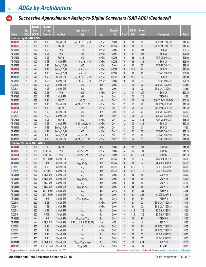
Amplifier and Data Converter Selection Guide Texas Instruments 3Q 2007
ADCs by Architecture
Successive Approximation Analog-to-Digital Converters (SAR ADC) (Continued)
62
Sample NumberRes. Rate of Input Input Voltage Linearity SINAD Power
Device (Bits) (kSPS) Channels Interface (V) VREF (%) NMC (dB) (mW) Package(s) Price*
Bipolar Input SAR ADCsADS8509 16 250 1 SE Serial, SPI +4, 10, ±3.3, 5, 10 Int/Ext 0.003 16 86 70 SOIC-20, SSOP-28 $12.95 ADS8505 16 250 1 SE P8/P16 ±10 Int/Ext 0.0022 16 86 70 SOIC-28, SSOP-28 $12.95 ADS7811 16 250 1 SE P16 ±2.5 Int/Ext 0.006 15 87 200 SOIC-28 $36.15 ADS7815 16 250 1 SE P16 ±2.5 Int/Ext 0.006 15 84 200 SOIC-28 $21.30 ADS7805 16 100 1 SE P8/P16 ±10 Int/Ext 0.0045 16 86 81.5 PDIP-28, SOIC-28 $25.00 ADS7809 16 100 1 SE Serial, SPI +4, 10, ±3.3, 5, 10 Int/Ext 0.0045 16 88 81.5 SOIC-20 $25.00 ADS7825 16 40 4 SE Serial, SPI/P8 ±10 Int/Ext 0.003 16 83 50 PDIP-28, SOIC-28 $29.55 ADS8507 16 40 1 SE Serial, SPI/P8 4, 5, ±10 Int/Ext 0.0022 16 89.9 24 SOIC-28 $13.00 ADS7807 16 40 1 SE Serial, SPI/P8 4, 5, ±10 Int/Ext 0.0022 16 88 28 PDIP-28, SOIC-28 $32.30 ADS8513 16 40 1 SE Serial, SPI +4, 10, ±3.3, 5, 10 Int/Ext 0.0023 16 89.9 30 SOIC-16 $12.00ADS7813 16 40 1 SE Serial, SPI +4, 10, ±3.3, 5, 10 Int/Ext 0.003 16 89 35 PDIP-16, SOIC-16 $24.70 TLC3578 14 200 8 SE Serial, SPI ±10 Ext 0.006 14 79 29 SOIC-24, TSSOP-24 $8.65 TLC3574 14 200 4 SE Serial, SPI ±10 Ext 0.006 14 79 29 SOIC-24, TSSOP-24 $6.85 ADS7810 12 800 1 SE P12 ±10 Int/Ext 0.018 12 71 225 SOIC-28 $27.80 ADS7835 12 500 1 SE Serial, SPI ±2.5 Int 0.024 12 72 17.5 VSSOP-8 $2.75 ADS7800 12 333 1 SE P8/P12 ±5, 10 Int 0.012 12 72 135 CDIP SB-24, PDIP-24 $30.50 ADS8508 12 250 1 SE Serial, SPI +4, 10, ±3.3, 5, 10 Int/Ext 0.011 12 73 70 SSOP-28, SOIC-20 $10.50 ADS8504 12 250 1 SE P8/P16 ±10 Int/Ext 0.011 12 72 70 SSOP-28, SOIC-28 $10.50 TLC2578 12 200 8 SE Serial, SPI ±10 Ext 0.024 12 79 29 SOIC-24, TSSOP-24 $5.80 TLC2574 12 200 4 SE Serial, SPI ±10 Ext 0.024 12 79 29 SOIC-20, TSSOP-20 $5.30 ADS7804 12 100 1 SE P8/P16 ±10 Int/Ext 0.011 12 72 81.5 PDIP-28, SOIC-28 $16.55 ADS7808 12 100 1 SE Serial, SPI +4, 10 , ±3.3, 5, 10 Int/Ext 0.011 12 73 81.5 SOIC-20 $12.80 ADS8506 12 80 1 SE Serial, SPI/P8 +4, 5, ±10 Int/Ext 0.011 12 73 24 SOIC-28 $8.50ADS7824 12 40 4 SE Serial, SPI/P8 ±10 Int/Ext 0.012 12 73 50 PDIP-28, SOIC-28 $13.10 ADS7806 12 40 1 SE Serial, SPI/P8 +4, 5, ±10 Int/Ext 0.011 12 73 28 PDIP-28, SOIC-28 $15.05 ADS7812 12 40 1 SE Serial, SPI +4, 10, ±3.3, 5, 10 Int/Ext 0.012 12 74 35 PDIP-16, SOIC-16 $11.80 General Purpose SAR ADCsADS8342 16 250 8 SE P8/P16 ±2.5 Ext 0.006 16 85 200 TQFP-48 $11.30 ADS8365 16 250 1 x 6 Diff P16 ±2.5V at +2.5 Int/Ext 0.006 14 87 190 TQFP-64 $16.25ADS8364 16 250 1 x 6 Diff P16 ±2.5V at +2.5 Int/Ext 0.009 14 82.5 413 TQFP-64 $18.10 ADS8326 16 250 1 SE, 1 PDiff Serial, SPI VREF Ext 0.0022 16 91 6 VSSOP-8, QFN-8 $5.00 ADS8317 16 200 1 Diff Serial, SPI ±VREF at VREF Ext 0.0022 16 88 6 VSSOP-8, SON-8 $5.90TLC4541 16 200 1 SE Serial, SPI VREF Ext 0.0038 16 84.5 17.5 SOIC-8, VSSOP-8 $6.85 TLC4545 16 200 1 PDiff Serial, SPI VREF Ext 0.0038 16 84.5 17.5 SOIC-8, VSSOP-8 $6.85 ADS8344 16 100 8 SE/4 Diff Serial, SPI VREF Ext 0.006 15 86 3.6 SSOP-20 $8.00 ADS8345 16 100 8 SE/4 Diff Serial, SPI ±VREF at VREF Ext 0.006 15 85 3.6 SSOP-20 $8.00 ADS8341 16 100 4 SE/2 Diff Serial, SPI VREF Ext 0.006 15 86 3.6 SSOP-16 $7.40 ADS8343 16 100 4 SE/2 Diff Serial, SPI ±VREF at VREF Ext 0.006 15 86 3.6 SSOP-16 $7.45 ADS8320 16 100 1 SE, 1 PDiff Serial, SPI VREF Ext 0.012 15 84 1.95 VSSOP-8 $5.15 ADS8325 16 100 1 SE, 1 PDiff Serial, SPI VREF Ext 0.006 16 91 2.25 VSSOP-8, QFN-8 $5.90 ADS8321 16 100 1 Diff Serial, SPI ±VREF at +VREF Ext 0.012 15 84 5.5 VSSOP-8 $5.15 TLC3548 14 200 8 SE Serial, SPI 4 Int/Ext 0.006 14 81 20 SOIC-24, TSSOP-24 $6.40 TLC3544 14 200 4 SE Serial, SPI 4 Int/Ext 0.006 14 81 20 SOIC-20, TSSOP-20 $6.00 TLC3541 14 200 1 SE Serial, SPI VREF Ext 0.006 14 81.5 17.5 SOIC-8, VSSOP-8 $5.00 TLC3545 14 200 1 PDiff Serial, SPI VREF Ext 0.006 14 81.5 17.5 SOIC-8, VSSOP-8 $5.00 ADS8324 14 50 1 Diff Serial, SPI ±VREF at +VREF Ext 0.012 14 78 2.5 VSSOP-8 $4.15 ADS7871 14 40 8 SE/4 Diff Serial, SPI PGA (1, 2, 4, 8, 10, 16, 20) Int 0.03 13 — 6 SSOP-28 $5.00 TLC2558 12 400 8 SE Serial, SPI 4 Int/Ext 0.024 12 71 9.5 SOIC-20, TSSOP-20 $5.30 TLC2554 12 400 4 SE Serial, SPI 4 Int/Ext 0.024 12 71 9.5 SOIC-16, TSSOP-16 $5.30 TLC2552 12 400 2 SE Serial, SPI VREF Ext 0.024 12 72 15 SOIC-8, VSSOP-8 $3.95 TLC2551 12 400 1 SE Serial, SPI VREF Ext 0.024 12 72 15 SOIC-8, VSSOP-8 $3.95 ADS7844 12 200 8 SE/4 Diff Serial, SPI VREF, ±VREF at VREF Ext 0.024 12 72 0.84 SSOP-20 $2.90 AMC7823 12 200 8 SE I/O DAS Serial, SPI VREF (5.0) Int/Ext 0.024 12 74 100 QFN-40 $9.75
*Suggested resale price in U.S. dollars in quantities of 1,000. New products are listed in bold red. Preview products are listed in bold blue.
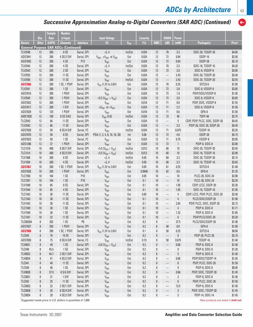
Texas Instruments 3Q 2007 Amplifier and Data Converter Selection Guide
ADCs by Architecture
Successive Approximation Analog-to-Digital Converters (SAR ADC) (Continued)
63
Sample NumberRes. Rate of Input Input Voltage Linearity SINAD Power
Device (Bits) (kSPS) Channels Interface (V) VREF (%) NMC (dB) (mW) Package(s) Price*
General Purpose SAR ADCs (Continued)TLV2548 12 200 8 SE Serial, SPI +2, 4 Int/Ext 0.024 12 70 3.3 SOIC-20, TSSOP-20 $4.85 ADS7841 12 200 4 SE/2 Diff Serial, SPI VREF , ±VREF at VREF Ext 0.024 12 72 0.84 SSOP-16 $2.50 ADS7842 12 200 4 SE P12 VREF Ext 0.024 12 72 0.84 SSOP-28 $3.10 TLV2544 12 200 4 SE Serial, SPI +2, 4 Int/Ext 0.024 12 70 3.3 SOIC-16, TSSOP-16 $4.20 TLV2542 12 200 2 SE Serial, SPI VREF Ext 0.024 12 72 2.8 SOIC-8, VSSOP-8 $3.85 TLV2553 12 200 11 SE Serial, SPI VREF Ext 0.024 12 — 2.43 SOIC-20, TSSOP-20 $3.40 TLV2556 12 200 11 SE Serial, SPI VREF Int/Ext 0.024 12 — 2.43 SOIC-20, TSSOP-20 $3.55 ADS7866 12 200 1 SE, 1 PDiff Serial, SPI VDD (1.2V to 3.6V) Ext 0.024 12 70 0.25 SOT23-6 $1.85 TLV2541 12 200 1 SE Serial, SPI VREF Ext 0.024 12 72 2.8 SOIC-8, VSSOP-8 $3.85 ADS7816 12 200 1 PDiff Serial, SPI VREF Ext 0.024 12 72 1.9 PDIP/SOIC/VSSOP-8 $1.95 TLV2545 12 200 1 PDiff Serial, SPI +5.5 (VREF = VDD) Ext 0.024 12 72 2.8 SOIC-8, VSSOP-8 $3.85 ADS7822 12 200 1 PDiff Serial, SPI VREF Ext 0.018 12 71 0.6 PDIP, SOIC, VSSOP-8 $1.55 ADS7817 12 200 1 Diff Serial, SPI ±VREF at +VREF Ext 0.024 12 71 2.3 SOIC-8, VSSOP-8 $1.95 ADS7829 12 125 1 PDiff Serial, SPI VREF Ext 0.018 12 71 0.6 QFN-8 $1.50 AMC7820 12 100 8 SE DAS Serial, SPI VREF (5.0) Int/Ext 0.024 12 72 40 TQFP-48 $3.75 TLC2543 12 66 11 SE Serial, SPI VREF Ext 0.024 12 — 5 CDIP, PDIP, PLCC, SOIC, SSOP-20 $4.45 TLV2543 12 66 11 SE Serial, SPI VREF Ext 0.024 12 — 3.3 PDIP-20, SOIC-20, SSOP-20 $4.45 ADS7828 12 50 8 SE/4 Diff Serial, I2C VREF Int/Ext 0.024 12 71 0.675 TSSOP-16 $3.35 ADS7870 12 50 8 SE Serial, SPI PGA (1, 2, 4, 8, 10, 16, 20) Int 0.06 12 72 4.6 SSOP-28 $4.15 ADS7823 12 50 1 SE Serial, I2C VREF Ext 0.024 12 71 0.75 VSSOP-8 $2.85 ADS1286 12 37 1 PDiff Serial, SPI VREF Ext 0.024 12 72 1 PDIP-8, SOIC-8 $2.80 TLC1518 10 400 8 SE/7 Diff Serial, SPI +5.5 (VREF = VDD) Int/Ext 0.012 10 60 10 SOIC-20, TSSOP-20 $3.45 TLC1514 10 400 4 SE/3 Diff Serial, SPI +5.5 (VREF = VDD) Int/Ext 0.012 10 60 10 SOIC-16, TSSOP-16 $2.90 TLV1508 10 200 8 SE Serial, SPI +2, 4 Int/Ext 0.05 10 60 3.3 SOIC-20, TSSOP-20 $3.15 TLV1504 10 200 4 SE Serial, SPI +2, 4 Int/Ext 0.05 10 60 3.3 SOIC-16, TSSOP-16 $2.65 ADS7867 10 200 1 SE, 1 PDiff Serial, SPI VDD (1.2V to 3.6V) Ext 0.05 10 61 0.25 SOT23-6 $1.40 ADS7826 10 200 1 PDiff Serial, SPI VREF Ext 0.0048 10 62 0.6 QFN-8 $1.25 TLC1550 10 164 1 SE P10 VREF Ext 0.05 10 — 10 PLCC-28, SOIC-24 $3.90 TLC1551 10 164 1 SE P10 VREF Ext 0.1 10 — 10 PLCC-28, SOIC-24 $3.35 TLV1548 10 85 8 SE Serial, SPI VREF Ext 0.1 10 — 1.05 CDIP, LCCC, SSOP-20 $2.30 TLV1544 10 85 4 SE Serial, SPI VREF Ext 0.1 10 — 1.05 SOIC-16, TSSOP-16 $1.95 TLC1542 10 38 11 SE Serial, SPI VREF Ext 0.05 10 — 4 CDIP, LCCC, PDIP, PLCC, SOIC-20 $2.50 TLC1543 10 38 11 SE Serial, SPI VREF Ext 0.1 10 — 4 PLCC/SOIC/SSOP-20 $1.90 TLV1543 10 38 11 SE Serial, SPI VREF Ext 0.1 10 — 2.64 PDIP, PLCC, SOIC, SSOP-20 $2.15 TLC1549 10 38 1 SE Serial, SPI VREF Ext 0.1 10 — 4 PDIP-8, SOIC-8 $1.71 TLV1549 10 38 1 SE Serial, SPI VREF Ext 0.1 10 — 1.32 PDIP-8, SOIC-8 $1.85 TLC1541 10 32 11 SE Serial, SPI VREF Ext 0.1 10 — 6 PDIP/PLCC/SOIC-20 $3.20 TLC0820A 8 392 1 SE P8 VREF Ext 0.2 8 — 37.5 PLCC/SOIC/SSOP-20 $1.90 ADS7827 8 250 1 PDiff Serial, SPI VREF Ext 0.2 8 48 0.6 QFN-8 $1.00 ADS7868 8 200 1 SE, 1 PDiff Serial, SPI VDD (1.2V to 3.6V) Ext 0.1 8 50 0.25 SOT23-6 $0.80 TLC545 8 76 19 SE Serial, SPI VREF Ext 0.2 8 — 6 PDIP-28, PLCC-28 $3.10 ADS7830 8 75 8 SE/4 Diff Serial, I2C VREF Int/Ext 0.19 8 50 0.675 TSSOP-16 $1.40 TLV0831 8 49 1 SE Serial, SPI +3.6 (VREF = VDD) Ext 0.2 8 — 0.66 PDIP-8, SOIC-8 $1.40 TLC548 8 45.5 1 SE Serial, SPI VREF Ext 0.2 8 — 9 PDIP-8, SOIC-8 $1.20 TLV0832 8 44.7 2 SE/1 Diff Serial, SPI VREF Ext 0.2 8 — 5 PDIP-8, SOIC-8 $1.40 TLV0834 8 41 4 SE/2 Diff Serial, SPI VREF Ext 0.2 8 — 0.66 PDIP/SOIC/TSSOP-14 $1.45 TLC541 8 40 11 SE Serial, SPI VREF Ext 0.2 8 — 6 PDIP, PLCC, SOIC-20 $1.50 TLC549 8 40 1 SE Serial, SPI VREF Ext 0.2 8 — 9 PDIP-8, SOIC-8 $0.95 TLV0838 8 37.9 8 S/4 Diff Serial, SPI VREF Ext 0.2 8 — 0.66 PDIP, SOIC, TSSOP-20 $1.45 TLC0831 8 31 1 Diff Serial, SPI VREF Ext 0.2 8 — 3 PDIP-8, SOIC-8 $1.40 TLC542 8 25 11 SE Serial, SPI VREF Ext 0.2 8 — 6 PDIP, PLCC, SOIC-20 $1.50 TLC0832 8 22 2 SE/1 Diff Serial, SPI VREF Ext 0.2 8 — 12.5 PDIP-8, SOIC-8 $1.40 TLC0838 8 20 8 SE/4 Diff Serial, SPI VREF Ext 0.2 8 — 3 PDIP, SOIC, TSSOP-20 $1.45 TLC0834 8 20 4 SE/2 Diff Serial, SPI VREF Ext 0.2 8 — 3 PDIP-14, SOIC-14 $1.45
*Suggested resale price in U.S. dollars in quantities of 1,000. New products are listed in bold red.
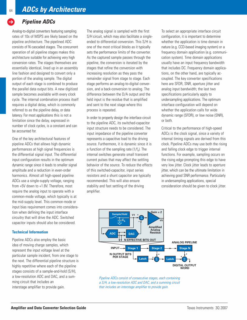
Amplifier and Data Converter Selection Guide Texas Instruments 3Q 2007
64 ADCs by Architecture
Pipeline ADCs
Analog-to-digital converters featuring samplingrates of 10s of MSPS are likely based on thepipeline architecture. The pipelined ADC consists of N cascaded stages. The concurrentoperation of all pipeline stages makes thisarchitecture suitable for achieving very highconversion rates. The stages themselves are essentially identical, lined up in an assemblyline fashion and designed to convert only aportion of the analog sample. The digital output of each stage is combined to producethe parallel data output bits. A new digitizedsample becomes available with every clockcycle. The internal combination process itselfrequires a digital delay, which is commonlyreferred to as the pipeline delay, or datalatency. For most applications this is not a limitation since the delay, expressed in number of clock cycles, is a constant and canbe accounted for.
One of the key architectural features ofpipeline ADCs that allows high dynamic performances at high signal frequencies isthe differential signal input. The differentialinput configuration results in the optimumdynamic range since it leads to smaller signalamplitude and a reduction in even-order harmonics. Almost all high-speed pipelineADCs use a single-supply voltage, rangingfrom +5V down to +1.8V. Therefore, mostrequire the analog input to operate with acommon-mode voltage, which typically is atthe mid-supply level. This common-mode orinput bias requirement comes into considera-tion when defining the input interface circuitry that will drive the ADC. Switchedcapacitor inputs should also be considered.
Technical Information
Pipeline ADCs also employ the basic idea of moving charge samples, which represent the input voltage level at the particular sample incident, from one stage tothe next. The differential pipeline structure ishighly repetitive where each of the pipelinestages consists of a sample-and-hold (S/H),a low-resolution ADC and DAC, and a sum-ming circuit that includes an interstage amplifier to provide gain.
The analog signal is sampled with the firstS/H circuit, which may also facilitate a single-ended to differential conversion. This S/H isone of the most critical blocks as it typicallysets the performance limits of the converter.As the captured sample passes through thepipeline, the conversion is iterated by thestages that refine the conversion withincreasing resolution as they pass theremainder signal from stage to stage. Eachstage performs an analog-to-digital conver-sion, and a back-conversion to analog. Thedifference between the D/A output and theheld input is the residue that is amplifiedand sent to the next stage where thisprocess is repeated.
In order to properly design the interface circuitto the pipeline ADC, its switched-capacitorinput structure needs to be considered. Theinput impedance of the pipeline converterrepresents a capacitive load to the drivingsource. Furthermore, it is dynamic since it isa function of the sampling rate (1/fs). Theinternal switches generate small transientcurrent pulses that may affect the settlingbehavior of the source. To reduce the effectsof this switched-capacitor, input series resistors and a shunt capacitor are typically recommended. This will also ensure stability and fast settling of the drivingamplifier.
To select an appropriate interface circuit configuration, it is important to determinewhether the application is time domain innature (e.g. CCD-based imaging system) or afrequency domain application (e.g. communi-cation system). Time domain applicationsusually have an input frequency bandwidththat includes DC. Frequency domain applica-tions, on the other hand, are typically ac-coupled. The key converter specificationshere are SFDR, SNR, aperture jitter and analog input bandwidth; the last two specifications particularly apply to undersampling applications. The optimuminterface configuration will depend onwhether the application calls for widedynamic range (SFDR), or low noise (SNR), or both.
Critical to the performance of high-speedADCs is the clock signal, since a variety ofinternal timing signals are derived from thisclock. Pipeline ADCs may use both the risingand falling clock edge to trigger internalfunctions. For example, sampling occurs onthe rising edge prompting this edge to havevery low jitter. Clock jitter leads to aperturejitter, which can be the ultimate limitation inachieving good SNR performance. Particularlyin undersampling applications, special consideration should be given to clock jitter.
Stage 1 Stage 2
Latch Latch
DAC
Sample/HoldGain = 2
AmplifiedAnalogResidue
V0
V1 +
+ +++
Cs
DIGITAL OUTPUT WORD
INPUT
N OUTPUT BITSPER STAGE
ANALOG PIPELINEN EFFECTIVE BITS OUT
Stage N
ADC
Pipeline ADCs consist of consecutive stages, each containinga S/H, a low-resolution ADC and DAC, and a summing circuitthat includes an interstage amplifier to provide gain.
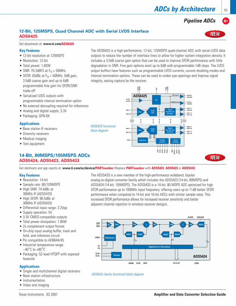
Texas Instruments 3Q 2007 Amplifier and Data Converter Selection Guide
ADCs by Architecture
Pipeline ADCs
65
Key Features• Resolution: 14-bit• Sample rate: 80/105MSPS• High SNR: 74.4dBc at
30MHz IF (ADS5433)• High SFDR: 96.5dBc at
30MHz IF (ADS5433)• Differential input range: 2.2Vpp• Supply operation: 5V• 3.3V CMOS-compatible outputs• Total power dissipation: 1.85W• 2s complement output format• On-chip input analog buffer, track and
hold, and reference circuit• Pin compatible to AD6644/45 • Industrial temperature range:
–40°C to +85°C• Packaging: 52-lead HTQFP with exposed
heatsink
Applications• Single and multichannel digital receivers• Base station infrastructure• Instrumentation• Video and imaging
14-Bit, 80MSPS/105MSPS ADCsADS5424, ADS5423, ADS5433
Get datsheets and app reports at: www.ti.com/sc/device/PARTnumber (Replace PARTnumber with ADS5424, ADS5423 or ADS5433)
ADS542x family functional block diagram.
The ADS5433 is a new member of the high-performance wideband, bipolar analog-to-digital converter family which includes the ADS5423 (14-bit, 80MSPS) andADS5424 (14-bit, 105MSPS). The ADS5433 is a 14-bit, 80 MSPS ADC optimized for highSFDR performance up to 100MHz input frequency; offering users up to 11dB better SFDRperformance when compared to 14-bit and 16-bit ADCs with similar sample rates. Thisincreased SFDR performance allows for increased receiver sensitivity and better adjacent channel rejection in wireless receiver designs.
A1
+
–
+
–
AIN
AIN
VREF
C1
C2
CLK+
CLK– Timing
Reference
TH1
5 5
Σ A3
AVDD DRVDD
ADC3
6
Digital Error Correction
DMID OVR DRY D[13:0] GND
ADC1 DAC1
TH2 A2
ADC2 DAC2
TH3Σ
ADS5424
AV
DD
AG
ND
CA
P
LVD
DLG
ND
IND_P
IND_M
INA_P
INA_M
CLKP
CLKM
VCM
DD1_M
DD1_P
DD0_M
DD0_P
DA1_M
DA1_P
DA0_M
DA0_P
FCLKM
FCLKP
DCLKP BIT Clock
FRAME Clock
Digital
Encoder and
Serializer
Digital
Encoder and
Serializer
12-Bit
ADC
12-Bit
ADC
Reference Parallel
Interface
Serial
Interface
PLL
DCLKM
RE
FP
RE
FM
PD
N
SE
N
CFG
1
SC
LK
SD
ATA
RE
SE
T
CFG
2
CFG
3
CFG
4
SHA
SHA
≈ ≈
12-Bit, 125MSPS, Quad Channel ADC with Serial LVDS Interface
ADS6425
Get datasheets at: www.ti.com/ADS6425
ADS6425 functional block diagram.
Key Features• 12-bit resolution at 125MSPS• Resolution: 12-bit• Total power: 1.65W• SNR: 70.3dBFS at FIN = 50MHz• SFDR: 83dBc at FIN = 50MHz, 0dB gain,
3.5dB coarse gain and up to 6dB programmable fine gain for SFDR/SNR trade-off
• Serialized LVDS outputs with programmable internal termination option
• No external decoupling required for references• Analog and digital supply: 3.3V• Packaging: QFN-64
Applications• Base station IF receivers• Diversity receivers• Medical imaging• Test equipment
The ADS6425 is a high-performance, 12-bit, 125MSPS quad-channel ADC with serial LVDS dataoutputs to reduce the number of interface lines to allow for higher system integration density. Itincludes a 3.5dB coarse gain option that can be used to improve SFDR performance with littledegradation in SNR. Fine gain options exist up to 6dB with programmable 1dB steps. The LVDSoutput buffers have features such as programmable LVDS currents, current doubling modes andinternal termination options. These can be used to widen eye-openings and improve signalintegrity, easing capture by the receiver.
ADS6425

Amplifier and Data Converter Selection Guide Texas Instruments 3Q 2007
ADCs by Architecture
Pipeline ADCs
66
SHA 14-Bit
ADC
CLOCKGEN
ReferenceControl
Interface
INP
INM
CLKP
CLKM
VCM
CLKOUTP
CLKOUTM
D0_D1_P
D0_D1_M
D2_D3_P
D4_D5_P
D6_D7_P
D8_D9_P
D10_D11_P
D12_D13_P
D2_D3_M
D4_D5_M
D6_D7_M
D8_D9_M
D10_D11_M
D12_D13_M
OVR
LVDS MODE
IRE
F
SC
LK
SE
N
SD
ATA
RE
SE
T OE
DF
S
MO
DE
AV
DD
AG
ND
DR
VD
D
DR
GN
D
Digital Encoder
and
Serializer
14-Bit, 170MSPS/190MSPS/210MSPS ADCs with LVDS/CMOS Outputs
ADS5545, ADS5546, ADS5547
Get datasheets at: www.ti.com/ADS5546, www.ti.com/ADS5545 or www.ti.com/sc/device/ADS5547
ADS5547 functional block diagram.
Key Features• SNR: 73.2dBc at 70MHz IF• SFDR: 84dBc at 70MHz IF• Total power disipation: 1.1W• DDR LVDS and parallel CMOS
output options• Internal/external reference support• Clock duty cycle stabilizer• 3.3V analog and digital supply• Packaging: QFN-48 (7x7mm)
Applications• Wireless communication infrastructure• Software-defined radio• Power amplifier linearization• Test and measurement• Medical imaging• Radar systems
The ADS5545, ADS5546, and ADS5547 are 14-bit, 170MSPS, 190MSPS and 210MSPS, respec-tively, ADCs that operate from a 3.3V supply and offer unprecedented digital output flexibility with fully differential double data rate (DDR) LVDS or parallel CMOS output options.Using an internal sample and hold and low jitter clock buffer, the three devices support highSNR and high SFDR at high IFs. The ADS5525 and ADS5527 are pin compatible 12-bit,170MSPS and 210MSPS versions of the ADS5545 and ADS5547, respectively.
ADS5547
ADC
ADC3
ADC2 DAC2ADC1 DAC1
Reference
Timing
Digital Error Correction
A1 TH1 TH2 A2 TH3 A3
555
∑∑
Monolithic 12-Bit, 500MSPS ADC
ADS5463
Get samples, datasheets, evaluation modules and app reports at: www.ti.com/sc/device/ADS5463
ADS5463 functional block diagram.
Key Features• 12-bit resolution at 500MSPS• SNR: 65.5dBFS at 100MHz fIN• SFDR: 80dBc at 100MHz fIN• 10.5-bit ENOB at 100MHz fIN• Analog operation: 5V and 3.3V, 3.3V digital• Total power dissipation: 2.25W• 3.3V LVDS outputs• 2.2Vpp input range; 2GHz input BW• Pin compatible with ADS5440, ADS5444• I-temp, Mil-temp enhanced plastic product
(114 x 114mm2), and space qualified package availability
• Packaging: TQFP-80
Applications• Test and measurement• Software-defined radio• Multi-channel base station receivers• Base station TX digital predistortion• Communications instrumentation
The new ADS5463 is the highest performing 12-bit monolithic ADC available with a 500MSPSsample rate while providing 65.5dBFS SNR and 80dBc SFDR through 100MHz fIN. Offered in aspace-saving 14mm x 14mm 80-pin TQFP package that is pin compatible to the 13-bit,210MSPS ADS5440 and 250MSPS ADS5444, the new ADC meets the resolution and speedrequirements for applications such as communications, amplifier linearization, test and measurement instrumentation, software-defined radio, radar and imaging systems.
ADS5463

Texas Instruments 3Q 2007 Amplifier and Data Converter Selection Guide
ADCs by Architecture
Pipeline ADCs
67
Pipeline ADCs Selection GuideSample # of Input Analog Input Supply
Res. Rate Input Voltage Bandwidth DNL INL SNR SFDR Voltage PowerDevice (Bits) (MSPS) Channels (V) (MHz) (± LSB) (± LSB) (dB) (dB) (V) (mW) Package(s) Price*
ADS5547 14 210 1 Diff 2 800 0.5 — 73.3 85 3, 3.6 1230 QFN-48 $82.50 ADS5546 14 190 1 Diff 2 500 0.5 3 73.2 84 3, 3.6 1130 QFN-48 $72.50 ADS5545 14 170 1 Diff 2 500 0.5 3 73.5 85 3, 3.6 1100 QFN-48 $62.50 ADS5500 14 125 1 Diff 2 750 1.1 5 70.5 82 3, 3.6 780 HTQFP-64 $49.00 ADS6245 14 125 2 Diff 2 500 2.5 5 73.2 83 3, 3.6 1000 QFN-48 $73.50 ADS6445 14 125 4 Diff 2 500 2.5 5 73.2 83 3, 3.6 1680 QFN-64 $132.30 ADS5424 14 105 1 Diff 2.2 570 –0.95, 1.5 1.5 74 93 4.75,5.25 1900 HTQFP-52 $56.00 ADS5541 14 105 1 Diff 2 750 –0.9, 1.1 5 72 85.1 3.0, 3.6 739 HTQFP-64 $41.00 ADS6244 14 105 2 Diff 2 500 2.5 5 73 81 3, 3.6 900 QFN-48 $61.50 ADS6444 14 105 4 Diff 2 500 2.5 5 73 81 3, 3.6 1350 QFN-64 $110.70 ADS5542 14 80 1 Diff 2 750 –0.9, 1.1 5 72.9 88 3.0, 3.6 674 HTQFP-64 $25.00 ADS5423 14 80 1 Diff 2.2 570 –0.95, 1.5 1.5 74 94 4.75,5.25 1850 HTQFP-52 $40.00 ADS5433 14 80 1 Diff 2.2 570 –0.95, 1.5 1.5 74 97.2 4.75,5.25 1850 HTQFP-52 $48.00 ADS6243 14 80 2 Diff 2 500 2 4.5 73.8 87.5 3, 3.6 760 QFN-48 $37.50 ADS6443 14 80 4 Diff 2 500 2 4.5 73.8 87.5 3, 3.6 1180 QFN-64 $71.25 ADS5553 14 65 2 Diff 2.3 750 1 4 74 84 3.0, 3.6 890 HTQFP-80 $30.00 ADS5422 14 62 1 Diff 2 to 4 300 1 — 72 85 4.75, 5.25 1200 LQFP-64 $30.45 ADS5421 14 40 1 Diff 2 to 4 300 1 — 75 83 4.75, 5.25 900 LQFP-64 $20.15 ADS850 14 10 1 SE/1 Diff 2 to 4 300 1 5 76 85 4.7, 5.3 250 TQFP-48 $10.50 THS1408 14 8 1 SE/1 Diff 1.5 140 1 5 72 80 3, 3.6 270 HTQFP-48, TQFP-48 $14.85 THS1403 14 3 1 SE/1 Diff 1.5 140 1 5 72 80 3, 3.6 270 HTQFP-48, TQFP-48 $11.05 THS14F03 14 3 1 SE/1 Diff 1.5 140 1 2.5 72 80 3, 3.6 270 TQFP-48 $12.60 THS1401 14 1 1 SE/1 Diff 1.5 140 1 5 72 80 3, 3.6 270 HTQFP-48, TQFP-48 $8.90 THS14F01 14 1 1 SE/1 Diff 1.5 140 1 2.5 72 80 3, 3.6 270 TQFP-48 $9.65 ADS5444 13 250 1 SE/1 Diff 2.2 800 — — 68.7 73 4.75, 5.25 2100 HTQFP-80 $59.00 ADS5440 13 210 1 SE/1 Diff 2.2 800 1 2.2 69 80 4.75, 5.25 2100 HTQFP-80 $42.00 ADS5463 12 500 1 Diff 2.2 2000 1 1.5 65.2 84 4.75, 5.25 2200 HTQFP-80 $125.00 ADS5527 12 210 1 Diff 2 800 0.5 — 69 81 3, 3.6 1100 QFN-48 $45.00 ADS5525 12 170 1 Diff 2 500 0.5 3 70.5 84 3, 3.6 1100 QFN-48 $35.00 ADS5520 12 125 1 Diff 2 750 0.5 1.5 69.7 83.6 3.0, 3.6 780 HTQFP-64 $27.50 ADS6225 12 125 2 Diff 2 500 2.5 5 70.3 83 3, 3.6 1000 QFN-48 $41.25 ADS6425 12 125 4 Diff 2 500 2.5 5 70.3 83 3, 3.6 1650 QFN-64 $74.25 ADS5521 12 105 1 DIff 2 750 0.5 1.5 70 86 3.0, 3.6 736 HTQFP-64 $23.00 ADS6224 12 105 2 Diff 2 500 2.5 5 70.6 81 3, 3.6 900 QFN-48 $34.50 ADS6424 12 105 4 Diff 2 500 2.5 5 70.6 81 3, 3.6 1350 QFN-64 $62.10 ADS5522 12 80 1 Diff 2 750 0.5 1.5 69.7 82.8 3.0, 3.6 663 HTQFP-64 $16.70 ADS5410 12 80 1 SE/1 Diff 2 1000 1 2 65 76 3, 3.6 360 TQFP-48 $19.00 ADS809 12 80 1 SE/1 Diff 1 to 2 1000 1.7 6 63 67 4.75, 5.25 905 TQFP-48 $24.95 ADS6223 12 80 2 Diff 2 500 2 4.5 70.9 87 3, 3.6 760 QFN-48 $25.05 ADS6423 12 80 4 Diff 2 500 2 4.5 70.9 87 3, 3.6 1180 QFN-64 $47.60 ADS808 12 70 1 SE/1 Diff 1 to 2 1000 1.7 7 64 68 4.75, 5.25 720 TQFP-48 $19.50 ADS5273 12 70 8 Diff 1.5 300 0.99, 1.2 3 71 85 3, 3.6 1003 HTQFP-80 $121.00 ADS5413 12 65 1 Diff 2 1000 1 2 68.5 79 3.0, 3.6 400 HTQFP-48 $14.75 ADS5221 12 65 1 SE/1 Diff 1 to 2 300 1 1.5 70 88 3.0, 3.6 285 TQFP-48 $13.95 ADS5232 12 65 2 Diff 2 300 0.9 2 70.7 86 3, 3.6 340 TQFP-64 $16.00 ADS5242 12 65 4 DIff 1.5 300 0.95, 1 2 71 85 3.0, 3.6 660 HTQFP-64 $30.00 ADS5272 12 65 8 Diff 1.5 300 0.95, 1 2 71.1 85 3, 3.6 984 HTQFP-80 $54.85 ADS807 12 53 1 SE/1 Diff 2 to 3 270 1 4 69 82 4.75, 5.25 335 SSOP-28 $11.30 ADS2807 12 50 2 SE/2 Diff 2 to 3 270 1 5 65 70 4.75, 5.25 720 TQFP-64 $18.05 ADS5271 12 50 8 Diff 1.5 300 0.9 2 70.5 85 3.0, 3.6 927 HTQFP-80 $48.00 ADS5220 12 40 1 SE/1 Diff 1 to 2 300 1 1.5 70 88 3.0, 3.6 195 TQFP-48 $9.85 ADS800 12 40 1 SE/1 Diff 2 65 1 — 62 61 4.75, 5.25 390 SO-28, TSSOP-28 $30.85 ADS5231 12 40 2 Diff 2 300 0.9 2 70.7 86 3, 3.6 285 TQFP-64 $11.75
*Suggested resale price in U.S. dollars in quantities of 1,000. New products are listed in bold red. Preview products are listed in bold blue.

Amplifier and Data Converter Selection Guide Texas Instruments 3Q 2007
ADCs by Architecture
Pipeline ADCs
68
Pipeline ADCs Selection Guide (Continued)Sample # of Input Analog Input Supply
Res. Rate Input Voltage Bandwidth DNL INL SNR SFDR Voltage PowerDevice (Bits) (MSPS) Channels (V) (MHz) (± LSB) (± LSB) (dB) (dB) (V) (mW) Package(s) Price*
ADS5240 12 40 4 Diff 1.5 300 0.9 2 70.5 85 3.0, 3.6 607 HTQFP-64 $20.00 ADS5270 12 40 8 Diff 1.5 300 0.9 2 70.5 85 3.0, 3.6 888 HTQFP-80 $44.00 ADS2806 12 32 2 SE/2 Diff 2 to 3 270 1 4 66 73 4.75, 5.25 430 TQFP-64 $14.10 THS1230 12 30 1 SE/1 Diff 1 to 2 180 1 2.5 67.7 74.6 3, 3.6 168 SOIC-28, TSSOP-28 $10.50 ADS801 12 25 1 SE/1 Diff 1 to 2 65 1 — 64 61 4.75, 5.25 270 SO-28, SSOP-28 $12.55 ADS805 12 20 1 SE/1 Diff 2 270 0.75 2 68 74 4.75, 5.25 300 SSOP-28 $9.90 THS1215 12 15 1 SE/1 Diff 1 to 2 180 0.9 1.5 68.9 81.7 3, 3.6 148 SOIC-28, SSOP-28 $9.85 ADS802 12 10 1 SE/1 Diff 2 65 1 2.75 66 66 4.75, 5.25 260 SO-28, SSOP-28 $12.60 ADS804 12 10 1 SE/1 Diff 2 270 0.75 2 69 80 4.7, 5.3 180 SSOP-28 $9.20 THS12082 12 8 2 SE/1 Diff 2.5 96 1 1.5 69 71 4.75, 5.25 186 TSSOP-32 $8.40 THS1209 12 8 2 SE/1 Diff 2.5 98 1 1.5 69 71 4.75, 5.25 186 TSSOP-32 $7.90 THS1206 12 6 4 SE/2 Diff 2.5 96 1 1.8 69 71 4.75, 5.25 186 TSSOP-32 $7.80 THS1207 12 6 4 SE/2 Diff 2.5 96 1 1.5 69 71 4.75, 5.25 186 TSSOP-32 $7.25 ADS803 12 5 1 SE/1 Diff 2 270 2 0.75 69 82 4.7, 5.3 115 SSOP-28 $7.40 ADS5510 11 125 1 Diff 2 750 1.1 5 66.8 83 3, 3.6 780 HTQFP-64 $14.20ADS5411 11 105 1 Diff 2.2 750 0.5 0.5 66.4 90 4.75, 5.25 1900 HTQFP-52 $25.50ADS5413-11 11 65 1 Diff 2 1000 0.75 1 65 77 3, 3.6 400 HTQFP-48 $14.75 ADS828 10 75 1 SE/1 Diff 2 300 1 3 57 68 4.75, 5.25 340 SSOP-28 $8.70 ADS5102 10 65 1 Diff 1 950 1 2.5 57 71 1.65, 2 160 TQFP-48 $7.10 ADS5277 10 65 8 Diff 1.5 300 0.5 1 61.7 85 3, 3.6 911 HTQFP-80 $32.00 ADS5122 10 65 8 Diff 1 22 1 2.5 59 72 1.65, 2.0 733 BGA-257 $42.85 ADS823 10 60 1 SE/1 Diff 2 300 1 2 60 74 4.75, 5.25 295 SSOP-28 $8.40 ADS826 10 60 1 SE/1 Diff 2 300 1 2 59 73 4.75, 5.25 295 SSOP-28 $8.40 ADS5103 10 40 1 Diff 1 950 0.8 1.5 58 66 1.65, 2 105 TQFP-48 $5.25 ADS821 10 40 1 SE/1 Diff 2 65 1 2 58 62 4.75, 5.25 390 SSOP-28, SO-28 $13.05 ADS822 10 40 1 SE/1 Diff 2 300 1 2 60 66 4.75, 5.25 200 SSOP-28 $5.25 ADS825 10 40 1 SE/1 Diff 2 300 1 2 60 65 4.75, 5.25 200 SSOP-28 $5.25 THS1040 10 40 1 SE/1 Diff 2 900 0.9 1.5 57 70 3, 3.6 100 SOIC-28, TSSOP-28 $5.10 THS1041 10 40 1 SE/1 Diff 2 900 1 1.5 57 70 3, 3.6 103 SOIC-28, TSSOP-28 $5.45 ADS5203 10 40 2 SE/2 Diff 1 300 1 1.5 60.5 73 3, 3.6 240 TQFP-48 $9.65 ADS5204 10 40 2 SE/2 Diff 2 300 1 1.5 60.5 73 3, 3.6 275 TQFP-48 $11.05 ADS5120 10 40 8 Diff 1 300 1 1.5 58 72 1.65, 2 794 BGA-257 $36.15 ADS5121 10 40 8 Diff 1 28 1 1.5 60 74 1.65, 2.0 500 BGA-257 $38.85 THS1030 10 30 1 SE/1 Diff 2 150 1 2 49.4 53 3, 5.5 150 SOIC-28, TSSOP-28 $3.75 THS1031 10 30 1 SE/1 Diff 2 150 1 2 49.3 52.4 3, 5.5 160 SOIC-28, TSSOP-28 $4.10 ADS820 10 20 1 SE/1 Diff 2 65 1 2 60 62 4.75, 5.25 200 SSOP-28, SO-28 $6.75 ADS900 10 20 1 SE/1 Diff 1 to 2 100 1 — 49 53 2.7, 3.7 54 SSOP-28 $3.55 ADS901 10 20 1 SE/1 Diff 1 to 2 100 1 — 53 49 2.7, 3.7 49 SSOP-28 $3.40 THS10082 10 8 2 SE/1 Diff 2.5 96 1 1 61 65 4.75, 5.25 186 TSSOP-32 $3.70 THS1009 10 8 2 SE/1 Diff +1.5, +3.5 96 1 1 61 65 4.75, 5.25 186 TSSOP-32 $3.20 THS10064 10 6 4 SE/2 Diff 2.5 96 1 1 61 65 4.75, 5.25 186 TSSOP-32 $4.15 THS1007 10 6 4 SE/2 Diff +1.5, +3.5 96 1 1 61 65 4.75, 5.25 186 TSSOP-32 $3.70 TLV1562 10 2 4 SE/2 Diff 3 120 1.5 1.5 58 70.3 2.7, 5.5 15 SOIC-28, TSSOP-28 $4.15 ADS831 8 80 1 SE/1 Diff 1 or 2 300 1 2 49 65 4.75, 5.25 310 SSOP-20 $3.15 ADS830 8 60 1 SE/1 Diff 1 or 2 300 1 1.5 49.5 65 4.75, 5.25 215 SSOP-20 $2.75 TLC5540 8 40 1 SE 2 75 1 1 44 42 4.75, 5.25 85 SOP-24, TSSOP-24 $1.99 THS0842 8 40 2 SE/2 Diff 1.3 600 2 2.2 42.7 52 3, 3.6 320 TQFP-48 $5.05 TLV5535 8 35 1 SE 1 to 1.6 600 1.3 2.4 46.5 58 3, 3.6 106 TSSOP-28 $2.40 ADS931 8 30 1 SE 1 to 4 100 1 2.5 48 49 2.7, 5.5 154 SSOP-28 $2.20 ADS930 8 30 1 SE/1 Diff 1 100 1 2.5 46 50 2.7, 5.25 168 SSOP-28 $2.30 TLC5510 8 20 1 SE 2 14 0.75 1 46 42 4.75, 5.25 127.5 SOP-24 $1.95 TLC5510A 8 20 1 SE 2 14 0.75 1 46 42 4.75, 5.25 150 SOP-24 $1.95
*Suggested resale price in U.S. dollars in quantities of 1,000. New products are listed in bold red.
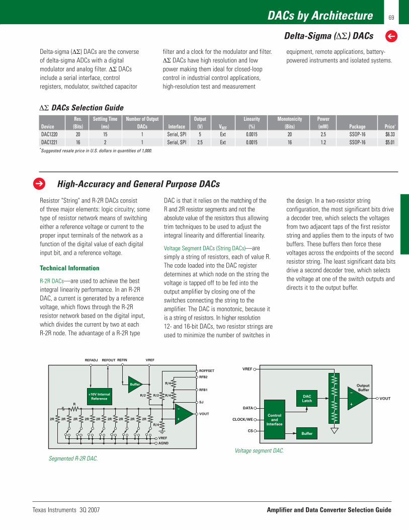
Texas Instruments 3Q 2007 Amplifier and Data Converter Selection Guide
DACs by Architecture
Delta-Sigma (∆Σ) DACs
69
Delta-sigma (∆Σ) DACs are the converse of delta-sigma ADCs with a digital modulator and analog filter. ∆Σ DACsinclude a serial interface, control registers, modulator, switched capacitor
filter and a clock for the modulator and filter.∆Σ DACs have high resolution and lowpower making them ideal for closed-loop control in industrial control applications,high-resolution test and measurement
equipment, remote applications, battery-powered instruments and isolated systems.
Resistor "String" and R-2R DACs consist of three major elements: logic circuitry; sometype of resistor network means of switchingeither a reference voltage or current to theproper input terminals of the network as afunction of the digital value of each digitalinput bit, and a reference voltage.
Technical Information
R-2R DACs—are used to achieve the bestintegral linearity performance. In an R-2RDAC, a current is generated by a referencevoltage, which flows through the R-2R resistor network based on the digital input,which divides the current by two at each R-2R node. The advantage of a R-2R type
DAC is that it relies on the matching of the R and 2R resistor segments and not theabsolute value of the resistors thus allowingtrim techniques to be used to adjust the integral linearity and differential linearity.
Voltage Segment DACs (String DACs)—are simply a string of resistors, each of value R.The code loaded into the DAC register determines at which node on the string thevoltage is tapped off to be fed into the output amplifier by closing one of theswitches connecting the string to the amplifier. The DAC is monotonic, because itis a string of resistors. In higher resolution12- and 16-bit DACs, two resistor strings areused to minimize the number of switches in
the design. In a two-resistor string configuration, the most significant bits drivea decoder tree, which selects the voltagesfrom two adjacent taps of the first resistorstring and applies them to the inputs of twobuffers. These buffers then force these voltages across the endpoints of the secondresistor string. The least significant data bitsdrive a second decoder tree, which selectsthe voltage at one of the switch outputs anddirects it to the output buffer.
Output Buffer
DATA
VREF
VOUT
CLOCK/WE
CSBuffer
DACLatch
Controland
Interface
Voltage segment DAC.
2R2R 2R 2R 2R 2R 2R 2R 2R
R/4
R/2R/2 R/4
R/4
R
ROFFSET
RFB2
RFB1
SJ
VOUT
VREF
VREF
AGND
REFINREFADJ REFOUT
+10V Internal
Reference
Buffer
Segmented R-2R DAC.
High-Accuracy and General Purpose DACs
∆Σ DACs Selection GuideRes. Settling Time Number of Output Output Linearity Monotonicity Power
Device (Bits) (ms) DACs Interface (V) VREF (%) (Bits) (mW) Package Price*
DAC1220 20 15 1 Serial, SPI 5 Ext 0.0015 20 2.5 SSOP-16 $6.33 DAC1221 16 2 1 Serial, SPI 2.5 Ext 0.0015 16 1.2 SSOP-16 $5.01
*Suggested resale price in U.S. dollars in quantities of 1,000.
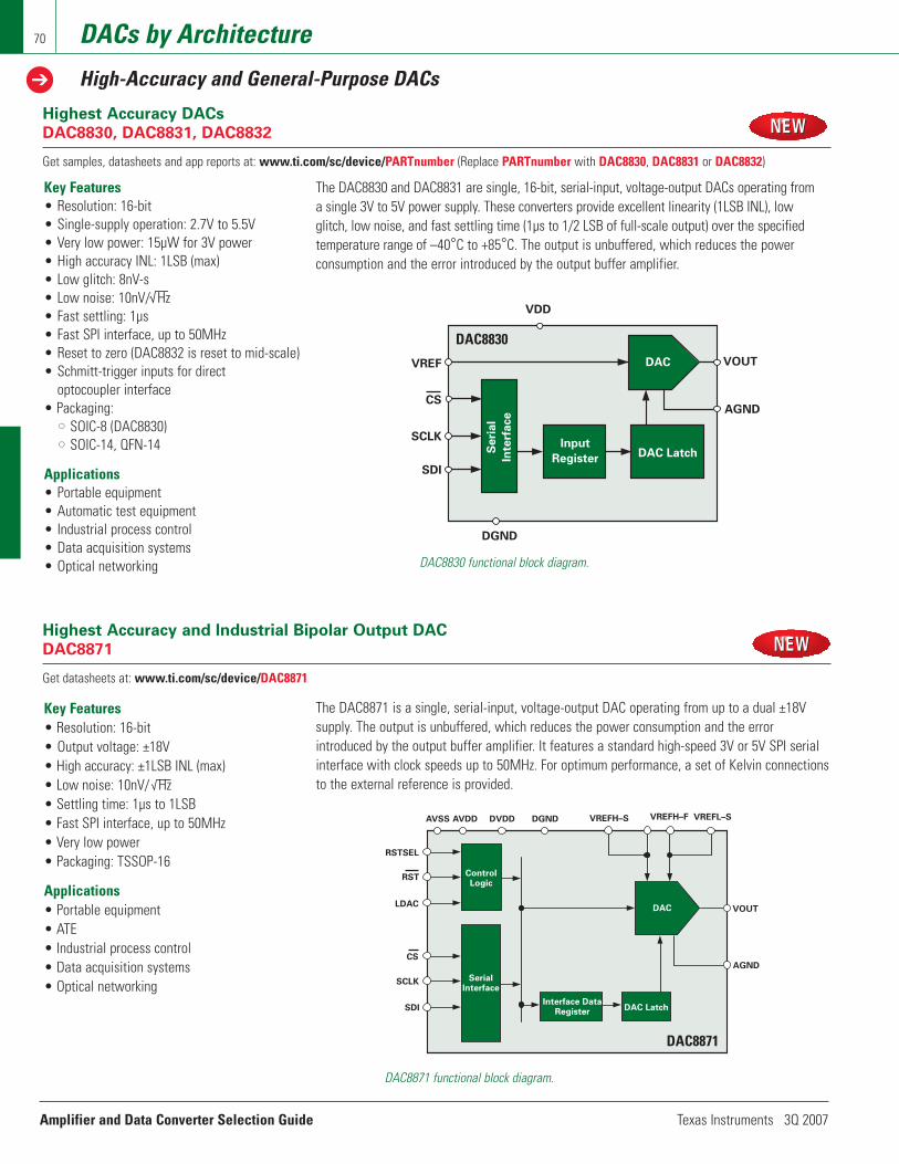
Amplifier and Data Converter Selection Guide Texas Instruments 3Q 2007
DACs by Architecture
High-Accuracy and General-Purpose DACs
70
AVSS
RSTSEL
RST
CS
SCLK
SDI
LDAC
AVDD DVDD
VOUT
AGND
DGND
VREFH–S VREFH–F VREFL–S
ControlLogic
Interface DataRegister
DAC Latch
DAC
SerialInterface
Highest Accuracy and Industrial Bipolar Output DAC
DAC8871
Get datasheets at: www.ti.com/sc/device/DAC8871
DAC8871 functional block diagram.
Key Features• Resolution: 16-bit• Output voltage: ±18V• High accuracy: ±1LSB INL (max)• Low noise: 10nV/ Hz• Settling time: 1µs to 1LSB• Fast SPI interface, up to 50MHz• Very low power• Packaging: TSSOP-16
Applications• Portable equipment• ATE• Industrial process control• Data acquisition systems• Optical networking
The DAC8871 is a single, serial-input, voltage-output DAC operating from up to a dual ±18Vsupply. The output is unbuffered, which reduces the power consumption and the error introduced by the output buffer amplifier. It features a standard high-speed 3V or 5V SPI serialinterface with clock speeds up to 50MHz. For optimum performance, a set of Kelvin connectionsto the external reference is provided.
DAC
SDI
SCLK
CS
VREF
DGND
VOUT
AGND
Se
ria
l
Inte
rfa
ce
Input
RegisterDAC Latch
VDD
DAC8830 functional block diagram.
Key Features• Resolution: 16-bit • Single-supply operation: 2.7V to 5.5V • Very low power: 15µW for 3V power• High accuracy INL: 1LSB (max)• Low glitch: 8nV-s• Low noise: 10nV/ Hz• Fast settling: 1µs• Fast SPI interface, up to 50MHz• Reset to zero (DAC8832 is reset to mid-scale)• Schmitt-trigger inputs for direct
optocoupler interface• Packaging:
•• SOIC-8 (DAC8830)•• SOIC-14, QFN-14
Applications• Portable equipment• Automatic test equipment• Industrial process control• Data acquisition systems• Optical networking
The DAC8830 and DAC8831 are single, 16-bit, serial-input, voltage-output DACs operating from a single 3V to 5V power supply. These converters provide excellent linearity (1LSB INL), low glitch, low noise, and fast settling time (1µs to 1/2 LSB of full-scale output) over the specifiedtemperature range of –40°C to +85°C. The output is unbuffered, which reduces the power consumption and the error introduced by the output buffer amplifier.
Highest Accuracy DACs
DAC8830, DAC8831, DAC8832
Get samples, datasheets and app reports at: www.ti.com/sc/device/PARTnumber (Replace PARTnumber with DAC8830, DAC8831 or DAC8832)
DAC8830
DAC8871
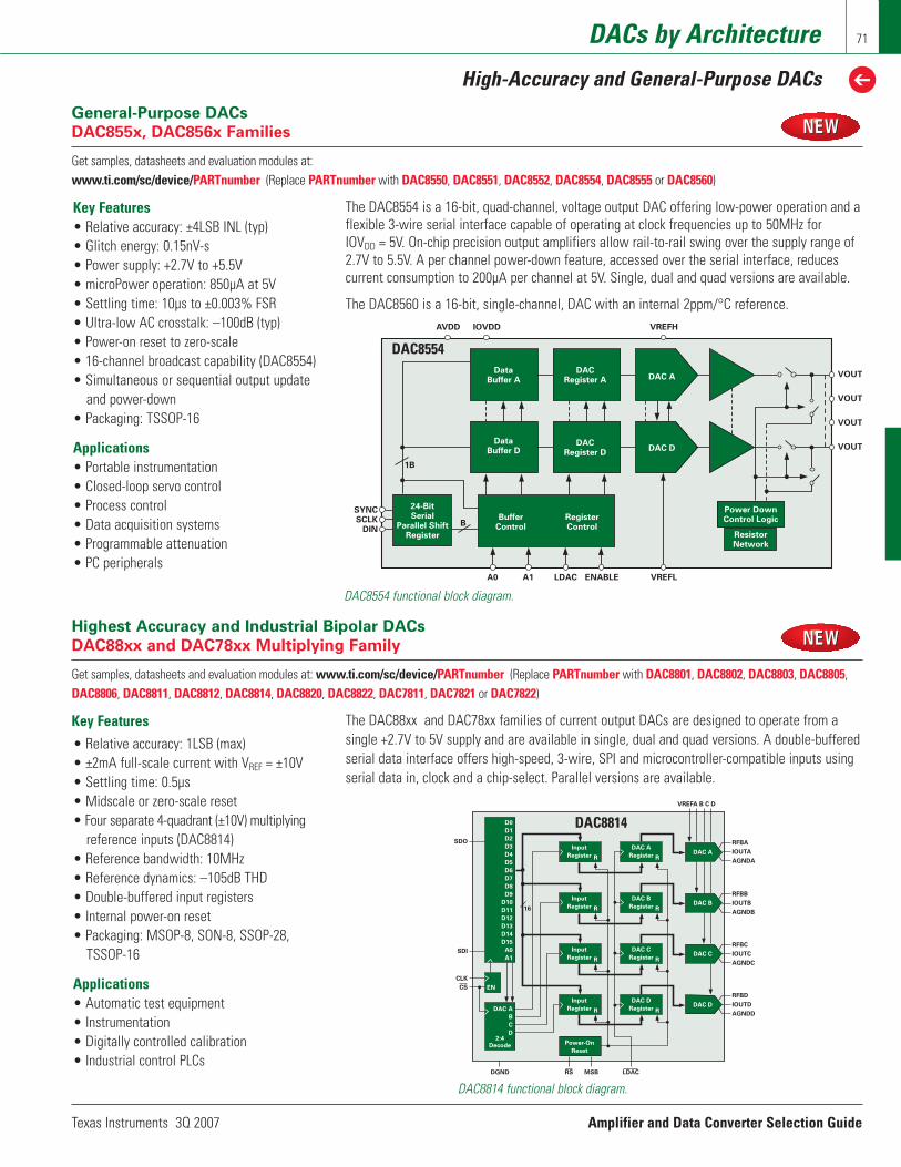
Texas Instruments 3Q 2007 Amplifier and Data Converter Selection Guide
DACs by Architecture
High-Accuracy and General-Purpose DACs
71
Power DownControl Logic
ResistorNetwork
RegisterControl
BufferControl
DataBuffer A
DataBuffer D
24-BitSerial
Parallel ShiftRegister
SYNCSCLK
DIN
1B
B
DACRegister A DAC A
DAC DDAC
Register D
VOUTA
VOUT
VOUT
VOUT
A0 A1 LDAC ENABLE VREFL
VREFHIOVDDAVDD
General-Purpose DACs
DAC855x, DAC856x Families
Get samples, datasheets and evaluation modules at: www.ti.com/sc/device/PARTnumber (Replace PARTnumber with DAC8550, DAC8551, DAC8552, DAC8554, DAC8555 or DAC8560)
DAC8554 functional block diagram.
Key Features• Relative accuracy: ±4LSB INL (typ)• Glitch energy: 0.15nV-s• Power supply: +2.7V to +5.5V• microPower operation: 850µA at 5V• Settling time: 10µs to ±0.003% FSR• Ultra-low AC crosstalk: –100dB (typ)• Power-on reset to zero-scale• 16-channel broadcast capability (DAC8554)• Simultaneous or sequential output update
and power-down• Packaging: TSSOP-16
Applications• Portable instrumentation• Closed-loop servo control• Process control• Data acquisition systems• Programmable attenuation• PC peripherals
The DAC8554 is a 16-bit, quad-channel, voltage output DAC offering low-power operation and aflexible 3-wire serial interface capable of operating at clock frequencies up to 50MHz for IOVDD = 5V. On-chip precision output amplifiers allow rail-to-rail swing over the supply range of2.7V to 5.5V. A per channel power-down feature, accessed over the serial interface, reducescurrent consumption to 200µA per channel at 5V. Single, dual and quad versions are available.
The DAC8560 is a 16-bit, single-channel, DAC with an internal 2ppm/°C reference.
DGND RS MSB LDAC
16
SDO
SDI
CLK
CS
DAC ARR
DAC A
Register
Input
Register
RR
DAC B
Register
Input
Register
RR
EN
DAC C
Register
Input
Register
RR
DAC D
Register
Input
Register
DAC B
DAC C
DAC D
Power-On
Reset
2:4Decode
DAC A
B
C
D
RFBA
IOUTA
AGNDA
RFBB
IOUTB
AGNDB
RFBC
IOUTC
AGNDC
RFBD
IOUTD
AGNDD
D0
D1
D2
D3
D4
D5
D6
D7
D8
D9
D10
D11
D12
D13
D14
D15
A0
A1
VREFA B C D
Highest Accuracy and Industrial Bipolar DACs
DAC88xx and DAC78xx Multiplying Family
Get samples, datasheets and evaluation modules at: www.ti.com/sc/device/PARTnumber (Replace PARTnumber with DAC8801, DAC8802, DAC8803, DAC8805,DAC8806, DAC8811, DAC8812, DAC8814, DAC8820, DAC8822, DAC7811, DAC7821 or DAC7822)
Key Features
DAC8814 functional block diagram.
• Relative accuracy: 1LSB (max)• ±2mA full-scale current with VREF = ±10V • Settling time: 0.5µs• Midscale or zero-scale reset• Four separate 4-quadrant (±10V) multiplying
reference inputs (DAC8814)• Reference bandwidth: 10MHz• Reference dynamics: –105dB THD• Double-buffered input registers• Internal power-on reset• Packaging: MSOP-8, SON-8, SSOP-28,
TSSOP-16
Applications• Automatic test equipment• Instrumentation• Digitally controlled calibration• Industrial control PLCs
The DAC88xx and DAC78xx families of current output DACs are designed to operate from asingle +2.7V to 5V supply and are available in single, dual and quad versions. A double-bufferedserial data interface offers high-speed, 3-wire, SPI and microcontroller-compatible inputs usingserial data in, clock and a chip-select. Parallel versions are available.
DAC8554
DAC8814
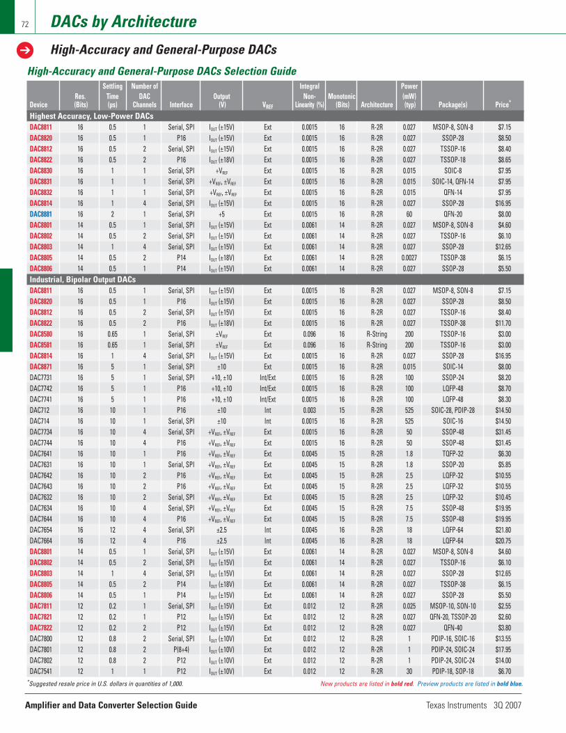
Amplifier and Data Converter Selection Guide Texas Instruments 3Q 2007
DACs by Architecture
High-Accuracy and General-Purpose DACs
72
High-Accuracy and General-Purpose DACs Selection GuideSettling Number of Integral Power
Res. Time DAC Output Non- Monotonic (mW)Device (Bits) (µs) Channels Interface (V) VREF Linearity (%) (Bits) Architecture (typ) Package(s) Price*
Highest Accuracy, Low-Power DACsDAC8811 16 0.5 1 Serial, SPI IOUT (±15V) Ext 0.0015 16 R-2R 0.027 MSOP-8, SON-8 $7.15 DAC8820 16 0.5 1 P16 IOUT (±15V) Ext 0.0015 16 R-2R 0.027 SSOP-28 $8.50 DAC8812 16 0.5 2 Serial, SPI IOUT (±15V) Ext 0.0015 16 R-2R 0.027 TSSOP-16 $8.40 DAC8822 16 0.5 2 P16 IOUT (±18V) Ext 0.0015 16 R-2R 0.027 TSSOP-18 $8.65DAC8830 16 1 1 Serial, SPI +VREF Ext 0.0015 16 R-2R 0.015 SOIC-8 $7.95 DAC8831 16 1 1 Serial, SPI +VREF, ±VREF Ext 0.0015 16 R-2R 0.015 SOIC-14, QFN-14 $7.95 DAC8832 16 1 1 Serial, SPI +VREF, ±VREF Ext 0.0015 16 R-2R 0.015 QFN-14 $7.95 DAC8814 16 1 4 Serial, SPI IOUT (±15V) Ext 0.0015 16 R-2R 0.027 SSOP-28 $16.95 DAC8881 16 2 1 Serial, SPI +5 Ext 0.0015 16 R-2R 60 QFN-20 $8.00 DAC8801 14 0.5 1 Serial, SPI IOUT (±15V) Ext 0.0061 14 R-2R 0.027 MSOP-8, SON-8 $4.60 DAC8802 14 0.5 2 Serial, SPI IOUT (±15V) Ext 0.0061 14 R-2R 0.027 TSSOP-16 $6.10 DAC8803 14 1 4 Serial, SPI IOUT (±15V) Ext 0.0061 14 R-2R 0.027 SSOP-28 $12.65 DAC8805 14 0.5 2 P14 IOUT (±18V) Ext 0.0061 14 R-2R 0.0027 TSSOP-38 $6.15DAC8806 14 0.5 1 P14 IOUT (±15V) Ext 0.0061 14 R-2R 0.027 SSOP-28 $5.50 Industrial, Bipolar Output DACsDAC8811 16 0.5 1 Serial, SPI IOUT (±15V) Ext 0.0015 16 R-2R 0.027 MSOP-8, SON-8 $7.15 DAC8820 16 0.5 1 P16 IOUT (±15V) Ext 0.0015 16 R-2R 0.027 SSOP-28 $8.50 DAC8812 16 0.5 2 Serial, SPI IOUT (±15V) Ext 0.0015 16 R-2R 0.027 TSSOP-16 $8.40 DAC8822 16 0.5 2 P16 IOUT (±18V) Ext 0.0015 16 R-2R 0.027 TSSOP-38 $11.70 DAC8580 16 0.65 1 Serial, SPI ±VREF Ext 0.096 16 R-String 200 TSSOP-16 $3.00 DAC8581 16 0.65 1 Serial, SPI ±VREF Ext 0.096 16 R-String 200 TSSOP-16 $3.00 DAC8814 16 1 4 Serial, SPI IOUT (±15V) Ext 0.0015 16 R-2R 0.027 SSOP-28 $16.95 DAC8871 16 5 1 Serial, SPI ±10 Ext 0.0015 16 R-2R 0.015 SOIC-14 $8.00DAC7731 16 5 1 Serial, SPI +10, ±10 Int/Ext 0.0015 16 R-2R 100 SSOP-24 $8.20 DAC7742 16 5 1 P16 +10, ±10 Int/Ext 0.0015 16 R-2R 100 LQFP-48 $8.70 DAC7741 16 5 1 P16 +10, ±10 Int/Ext 0.0015 16 R-2R 100 LQFP-48 $8.30 DAC712 16 10 1 P16 ±10 Int 0.003 15 R-2R 525 SOIC-28, PDIP-28 $14.50 DAC714 16 10 1 Serial, SPI ±10 Int 0.0015 16 R-2R 525 SOIC-16 $14.50 DAC7734 16 10 4 Serial, SPI +VREF, ±VREF Ext 0.0015 16 R-2R 50 SSOP-48 $31.45 DAC7744 16 10 4 P16 +VREF, ±VREF Ext 0.0015 16 R-2R 50 SSOP-48 $31.45 DAC7641 16 10 1 P16 +VREF, ±VREF Ext 0.0045 15 R-2R 1.8 TQFP-32 $6.30 DAC7631 16 10 1 Serial, SPI +VREF, ±VREF Ext 0.0045 15 R-2R 1.8 SSOP-20 $5.85 DAC7642 16 10 2 P16 +VREF, ±VREF Ext 0.0045 15 R-2R 2.5 LQFP-32 $10.55 DAC7643 16 10 2 P16 +VREF, ±VREF Ext 0.0045 15 R-2R 2.5 LQFP-32 $10.55 DAC7632 16 10 2 Serial, SPI +VREF, ±VREF Ext 0.0045 15 R-2R 2.5 LQFP-32 $10.45 DAC7634 16 10 4 Serial, SPI +VREF, ±VREF Ext 0.0045 15 R-2R 7.5 SSOP-48 $19.95 DAC7644 16 10 4 P16 +VREF, ±VREF Ext 0.0045 15 R-2R 7.5 SSOP-48 $19.95 DAC7654 16 12 4 Serial, SPI ±2.5 Int 0.0045 16 R-2R 18 LQFP-64 $21.80 DAC7664 16 12 4 P16 ±2.5 Int 0.0045 16 R-2R 18 LQFP-64 $20.75 DAC8801 14 0.5 1 Serial, SPI IOUT (±15V) Ext 0.0061 14 R-2R 0.027 MSOP-8, SON-8 $4.60 DAC8802 14 0.5 2 Serial, SPI IOUT (±15V) Ext 0.0061 14 R-2R 0.027 TSSOP-16 $6.10 DAC8803 14 1 4 Serial, SPI IOUT (±15V) Ext 0.0061 14 R-2R 0.027 SSOP-28 $12.65 DAC8805 14 0.5 2 P14 IOUT (±18V) Ext 0.0061 14 R-2R 0.027 TSSOP-38 $6.15DAC8806 14 0.5 1 P14 IOUT (±15V) Ext 0.0061 14 R-2R 0.027 SSOP-28 $5.50 DAC7811 12 0.2 1 Serial, SPI IOUT (±15V) Ext 0.012 12 R-2R 0.025 MSOP-10, SON-10 $2.55 DAC7821 12 0.2 1 P12 IOUT (±15V) Ext 0.012 12 R-2R 0.027 QFN-20, TSSOP-20 $2.60 DAC7822 12 0.2 2 P12 IOUT (±15V) Ext 0.012 12 R-2R 0.027 QFN-40 $3.80 DAC7800 12 0.8 2 Serial, SPI IOUT (±10V) Ext 0.012 12 R-2R 1 PDIP-16, SOIC-16 $13.55 DAC7801 12 0.8 2 P(8+4) IOUT (±10V) Ext 0.012 12 R-2R 1 PDIP-24, SOIC-24 $17.95 DAC7802 12 0.8 2 P12 IOUT (±10V) Ext 0.012 12 R-2R 1 PDIP-24, SOIC-24 $14.00 DAC7541 12 1 1 P12 IOUT (±10V) Ext 0.012 12 R-2R 30 PDIP-18, SOP-18 $6.70
*Suggested resale price in U.S. dollars in quantities of 1,000. New products are listed in bold red. Preview products are listed in bold blue.

Texas Instruments 3Q 2007 Amplifier and Data Converter Selection Guide
DACs by Architecture
High-Accuracy and General-Purpose DACs
73
High-Accuracy and General-Purpose DACs Selection Guide (Continued)Settling Number of Integral Power
Res. Time DAC Output Non- Monotonic (mW)Device (Bits) (µs) Channels Interface (V) VREF Linearity (%) (Bits) Architecture (typ) Package(s) Price*
Industrial Bipolar Output DACs (continued)DAC8043 12 1 1 Serial, SPI IOUT (±10V) Ext 0.012 12 R-2R 2.5 SOIC-8 $3.60 DAC7545 12 2 1 P12 IOUT (±10V) Ext 0.012 12 R-2R 30 SOIC-20 $5.25 DAC811 12 4 1 P12 +10, ±5, 10 Int 0.006 12 R-2R 625 CDIP SB-28, PDIP-28, $11.00
SOIC-28DAC813 12 4 1 P12 +10, ±5, 10 Int/Ext 0.006 12 R-2R 270 PDIP-28, SOIC-28 $12.60 DAC7613 12 10 1 P12 +VREF, ±VREF Ext 0.024 12 R-2R 1.8 SSOP-24 $2.50 DAC7614 12 10 4 Serial, SPI +VREF, ±VREF Ext 0.024 12 R-2R 15 PDIP-16, SOIC-16, SSOP-20 $6.70 DAC7615 12 10 4 Serial, SPI +VREF, ±VREF Ext 0.024 12 R-2R 15 PDIP-16, SOIC-16, SSOP-20 $6.70 DAC7616 12 10 4 Serial, SPI +VREF, ±VREF Ext 0.024 12 R-2R 2.4 SOIC-16, SSOP-20 $5.40 DAC7617 12 10 4 Serial, SPI +VREF, ±VREF Ext 0.024 12 R-2R 2.4 SOIC-16, SSOP-20 $5.40 DAC7624 12 10 4 P12 +VREF, ±VREF Ext 0.024 12 R-2R 15 PDIP-28, SOIC-28 $10.25 DAC7625 12 10 4 P12 +VREF, ±VREF Ext 0.024 12 R-2R 15 PDIP-28, SOIC-28 $10.25 DAC7714 12 10 4 Serial, SPI +VREF, ±VREF Ext 0.024 12 R-2R 45 SOIC-16 $11.45 DAC7715 12 10 4 Serial, SPI +VREF, ±VREF Ext 0.024 12 R-2R 45 SOIC-16 $11.45 DAC7724 12 10 4 P12 +VREF, ±VREF Ext 0.024 12 R-2R 45 PLCC-28, SOIC-28 $11.85 DAC7725 12 10 4 P12 +VREF, ±VREF Ext 0.024 12 R-2R 45 PLCC-28, SOIC-28 $11.85 TLC7524 8 0.1 1 P8 IOUT (±10V) Ext 0.2 8 R-2R 5 PDIP-16, PLCC-20, $1.45
SOIC-16, TSSOP-16TLC7528 8 0.1 2 P8 IOUT (±10V) Ext 0.2 8 R-2R 7.5 PDIP-20, PLCC-20, $1.55
SOIC-20, TSSOP-20TLC7628 8 0.1 2 P8 IOUT (±10V) Ext 0.2 8 R-2R 20 SOIC-20, PDIP-20 $1.45 TLC7225 8 5 4 P8 +VREF Ext 0.4 8 R-2R 75 SOIC-24 $2.35 TLC7226 8 5 4 P8 +VREF Ext 0.4 8 R-2R 90 PDIP-20, SOIC-20 $2.15 General-Purpose DACsDAC8550 16 10 1 Serial, SPI +VREF Ext 0.012 16 R-String 1 MSOP-8 $2.65 DAC8551 16 10 1 Serial, SPI +VREF Ext 0.012 16 R-String 1 VSSOP-8, QFN 3 x 3 $2.65 DAC8560 16 10 1 Serial, SPI +VREF (+2.5) Int/Ext 0.012 16 R-String 2.6 MSOP-8 $3.50 DAC8564 16 10 4 Serial, SPI +VREF (+2.5) Int/Ext 0.012 16 R-String 5 MSOP-8 $10.45 DAC8565 16 10 4 Serial, SPI +VREF (+2.5) Int/Ext 0.012 16 R-String 5 MSOP-8 $10.45DAC8501 16 10 1 Serial, SPI +VREF/MDAC Ext 0.0987 16 R-String 0.72 MSOP-8 $3.00 DAC8531 16 10 1 Serial, SPI +VREF Ext 0.0987 16 R-String 0.72 MSOP-8, SON-8 $3.00 DAC8541 16 10 1 P16 +VREF Ext 0.096 16 R-String 0.72 TQFP-32 $3.00 DAC8571 16 10 1 Serial, I2C +VREF Ext 0.0987 16 R-String 0.42 MSOP-8 $2.95 DAC8552 16 10 2 Serial, SPI +VREF Ext 0.012 16 R-String 2 MSOP-8 $5.45 DAC8532 16 10 2 Serial, SPI +VREF Ext 0.0987 16 R-String 1.35 MSOP-8 $5.35 DAC8554 16 10 4 Serial, SPI +VREF Ext 0.012 16 R-String 4 TSSOP-16 $10.40 DAC8555 16 10 4 Serial, SPI +VREF Ext 0.012 16 R-String 4 TSSOP-16 $10.40 DAC8544 16 10 4 P16 +VREF Ext 0.098 16 R-String 2 TQFP-48 $9.75 DAC8534 16 10 4 Serial, SPI +VREF Ext 0.0987 16 R-String 2.7 TSSOP-16 $8.75 DAC8574 16 10 4 Serial, I2C +VREF Ext 0.0987 16 R-String 2.7 TSSOP-16 $10.25 DAC715 16 10 1 P16 +10 Int 0.003 16 R-2R 525 PDIP-28, SOIC-28 $15.85 DAC716 16 10 1 Serial, SPI +10 Int 0.003 16 R-2R 525 PDIP-16, SOIC-16 $15.85 TLV5613 12 1 1 P8 +VREF Ext 0.096 12 R-String 1.2 SOIC-20, TSSOP-20 $2.60 TLV5619 12 1 1 P12 +VREF Ext 0.096 12 R-String 4.3 SOIC-20, TSSOP-20 $2.60 TLV5633 12 1 1 P8 +VREF (+2, 4) Int/Ext 0.072 12 R-String 2.7 SOIC-20, TSSOP-20 $4.70 TLV5636 12 1 1 Serial, SPI +VREF (+2, 4) Int/Ext 0.096 12 R-String 4.5 SOIC-8, VSSOP-8 $3.65 TLV5639 12 1 1 P12 +VREF (+2, 4) Int/Ext 0.072 12 R-String 2.7 SOIC-20, TSSOP-20 $3.45 TLV5638 12 1 2 Serial, SPI +VREF (+2, 4) Int/Ext 0.096 12 R-String 4.5 SOIC-8, CDIP-8, LCCC-20 $3.25 TLV5610 12 1 8 Serial, SPI +VREF Ext 0.144 12 R-String 18 SOIC-20, TSSOP-20 $8.50 TLV5630 12 1 8 Serial, SPI +VREF Int/Ext 0.144 12 R-String 18 SOIC-20, TSSOP-20 $8.85 TLV5618A 12 2.5 2 Serial, SPI +VREF Ext 0.096 12 R-String 1.8 CDIP-8, PDIP-8, $4.75
SOIC-8, LCCC-20TLV5616 12 3 1 Serial, SPI +VREF Ext 0.096 12 R-String 0.9 VSSOP-8, PDIP-8, SOIC-8 $2.60
*Suggested resale price in U.S. dollars in quantities of 1,000. New products are listed in bold red. Preview products are listed in bold blue.

Amplifier and Data Converter Selection Guide Texas Instruments 3Q 2007
DACs by Architecture
High-Accuracy and General-Purpose DACs
74
High-Accuracy and General-Purpose DACs Selection Guide (Continued)Settling Number of Integral Power
Res. Time DAC Output Non- Monotonic (mW)Device (Bits) (µs) Channels Interface (V) VREF Linearity (%) (Bits) Architecture (typ) Package(s) Price*
General-Purpose DACs (continued)TLV5614 12 3 4 Serial, SPI +VREF Ext 0.096 12 R-String 3.6 SOIC-16, TSSOP-16 $7.45 DAC7551 12 5 1 Serial, SPI +VREF Ext 0.024 12 R-String 0.27 SON-12 $1.40 DAC7552 12 5 2 Serial, SPI +VREF Ext 0.024 12 R-String 0.675 QFN-16 $2.35 DAC7553 12 5 2 Serial, SPI +VREF Ext 0.024 12 R-String 0.675 QFN-16 $2.35 DAC7554 12 5 4 Serial, SPI +VREF Ext 0.024 12 R-String 1.5 MSOP-10 $4.80 DAC7558 12 5 8 Serial, SPI +VREF Ext 0.024 12 String 2.7 QFN-32 $7.50 DAC7611 12 7 1 Serial, SPI +4.096 Int 0.012 12 R-2R 2.5 PDIP-8, SOIC-8 $2.55 DAC7621 12 7 1 P12 +4.096 Int 0.012 12 R-2R 2.5 SSOP-20 $2.75 DAC7612 12 7 2 Serial, SPI +4.096 Int 0.012 12 R-2R 3.5 SOIC-8 $3.10 DAC7512 12 10 1 Serial, SPI +VDD Ext 0.192 12 R-String 0.34 MSOP-8, SOT23-6 $1.45 DAC7513 12 10 1 Serial, SPI +VREF Ext 0.192 12 R-String 0.3 MSOP-8, SOT23-8 $1.65 DAC7571 12 10 1 Serial, I2C +VREF Ext 0.192 12 R-String 0.86 SOT23-6 $1.55 DAC7573 12 10 4 Serial, I2C +VREF Ext 0.192 12 R-String 1.8 TSSOP-16 $6.15 DAC7574 12 10 4 Serial, I2C +VREF Ext 0.192 12 R-String 1.8 MSOP-10 $6.15 TLV5637 10 0.8 2 Serial, SPI +VREF (+2, 4) Int/Ext 0.098 10 R-String 4.2 SOIC-8 $3.20 TLV5608 10 1 8 Serial, SPI +VREF Ext 0.59 10 R-String 18 SOIC-20, TSSOP-20 $4.90 TLV5631 10 1 8 Serial, SPI +VREF Int/Ext 0.196 10 R-String 18 SOIC-20, TSSOP-20 $5.60 TLV5617A 10 2.5 2 Serial, SPI +VREF Ext 0.098 10 R-String 1.8 SOIC-8 $2.25 TLV5606 10 3 1 Serial, SPI +VREF Ext 0.147 10 R-String 0.9 SOIC-8, MSOP-8 $1.30 TLV5604 10 3 4 Serial, SPI +VREF Ext 0.05 10 R-String 3 SOIC-16, TSSOP-16 $3.70 DAC6571 10 9 1 Serial, I2C +VDD Ext 0.196 10 R-String 0.5 SOT23-6 $1.40 DAC6573 10 9 4 Serial, I2C +VREF Ext 0.196 10 R-String 1.5 TSSOP-16 $3.05 DAC6574 10 9 4 Serial, I2C +VREF Ext 0.196 10 R-String 1.5 MSOP-10 $3.05 TLC5615 10 12.5 1 Serial, SPI +VREF Ext 0.098 10 R-String 0.75 PDIP-8, SOIC-8 $1.90 TLV5626 8 0.8 2 Serial, SPI +VREF (+2, 4) Int/Ext 0.391 8 R-String 4.2 SOIC-8 $1.90 TLV5624 8 1 1 Serial, SPI +VREF (+2, 4) Int/Ext 0.196 8 R-String 5 SOIC-8, MSOP-8 $1.60 TLV5629 8 1 8 Serial, SPI +VREF Ext 0.391 8 R-String 18 SOIC-20, TSSOP-20 $3.15 TLV5632 8 1 8 Serial, SPI +VREF (+2, 4) Int/Ext 0.391 8 R-String 18 SOIC-20, TSSOP-20 $3.35 TLV5627 8 2.5 4 Serial, SPI +VREF Ext 0.196 8 R-String 3 SOIC-16, TSSOP-16 $2.05 TLV5623 8 3 1 Serial, SPI +VREF Ext 0.196 8 R-String 2.1 SOIC-8, MSOP-8 $0.99 TLV5625 8 3 2 Serial, SPI +VREF Ext 0.196 8 R-String 2.4 SOIC-8 $1.70 DAC5571 8 8 1 Serial, I2C +VDD Int 0.196 8 R-String 0.5 SOT23-6 $0.90 DAC5573 8 8 4 Serial, I2C +VREF Ext 0.196 8 R-String 1.5 TSSOP-16 $2.55 DAC5574 8 8 4 Serial, I2C +VREF Ext 0.196 8 R-String 1.5 MSOP-10 $2.55 TLC5620 8 10 4 Serial, SPI +VREF Ext 0.391 8 R-String 8 PDIP-14, SOIC-14 $1.75 TLV5620 8 10 4 Serial, SPI +VREF Ext 0.391 8 R-2R 6 PDIP-14, SOIC-14 $1.00 TLV5621 8 10 4 Serial, SPI +VREF Ext 0.391 8 R-2R 3.6 SOIC-14 $1.65 TLC5628 8 10 8 Serial, SPI +VREF Ext 0.391 8 R-String 15 PDIP-16, SOIC-16 $2.45 TLV5628 8 10 8 Serial, SPI +VREF Ext 0.391 8 R-String 12 PDIP-16, SOIC-16 $2.20
*Suggested resale price in U.S. dollars in quantities of 1,000. New products are listed in bold red.
Settling

Texas Instruments 3Q 2007 Amplifier and Data Converter Selection Guide
DACs by Architecture
Current Steering DACs
75
Opt. 2x – 32x
Clock Multiplier PLL
Clock Generation
16
8 S
am
ple
Inp
ut
FIF
O &
Dem
ux
x2
Optional 4c
Interpolation FIR
x2
Optional 2c
Interpolation FIR
Control
16x2 x2
Op
tio
na
l F
s/4
Mix
er
16-bit
DAC
16-bit
DAC
1.2V
Reference
DACCLK
DACCLK
DCCLP
DCCLB
D15P
D15N
DOP
DON
SYNCN
SYNCP
IOUTA1
IOUTA2
IOUTB1
IOUTB2
SD
IO
SD
O
SD
EN
B
SC
LK
RE
SE
TB
16-Bit, 1GSPS Dual DAC
DAC5682Z
Get samples, datasheets, evaluation modules and app reports at: www.ti.com/sc/device/DAC5682Z
DAC5682Z functional block diagram.
Key Features• 16-bit LVDS input data bus• 8 sample input FIFO• Interleaved IQ data for dual DAC mode• Superior ACLR/ACPR performance• 2x-32x clock multiplying PLL• 2x or 4x selectable interpolation filters• Configurable low pass/high pass option• Fs/4 mixer• Scalable differential outputs: 2 to 20mA• Package 64-pin QFN (9x9)
Applications• Cellular base stations• Broadband wireless access• WiMAX / 802.16• Fixed wireless backhaul• Cable modem termination systems• Test equipment
The DAC5682Z is designed to enable the conversion of wide bandwidth signals from digital toanalog. The LVDS interface enables the input of high data rates while controlling EMI emissionsand reducing footprint size of the device. Several configurable features the device also savecost, such as the on-board multiplying clock which eliminates the use of expensive off-chipclocking. In addition, the low-pass/high-pass interpolation filters and digital mixer optionsenables system design flexibility.
Modern high-speed DACs, fabricated on submicron CMOS or BiCMOS processes,have reached new performance levels withupdate rates of 500MSPS and resolutions of14- or even 16-bits. In order to realize suchhigh update rates and resolutions, the DACsemploy a current-steering architecture with segmented current sources. The core elementwithin the monolithic DAC is the currentsource array designed to deliver the full-scaleoutput current, typically 20mA. An internaldecoder addresses the differential currentswitches each time the DAC is updated.Steering the currents from all currentsources to either of the differential
outputs forms a corresponding signal outputcurrent. Differential signaling is used toimprove the dynamic performance whilereducing the output voltage swing that isdeveloped across the load resistors. Ideally,this signal voltage amplitude should be assmall as possible to maintain optimum linearityof the DAC. The upper limit of this signalvoltage, and consequently the load resistance,is defined by the output voltage compliancespecification.
The segmented current-steering architecture provides a significant reduction in circuit complexity and consequently in reducedglitch energy. This translates into an overall
improvement of the DAC’s linearity and ac performance. As new system architecturesrequire the synthesis of output frequencies in the 100s of MHz range, an approach oftenreferred to as “direct IF” achieves highupdate rates, while maintaining excellentdynamic performance.
DAC5682Z
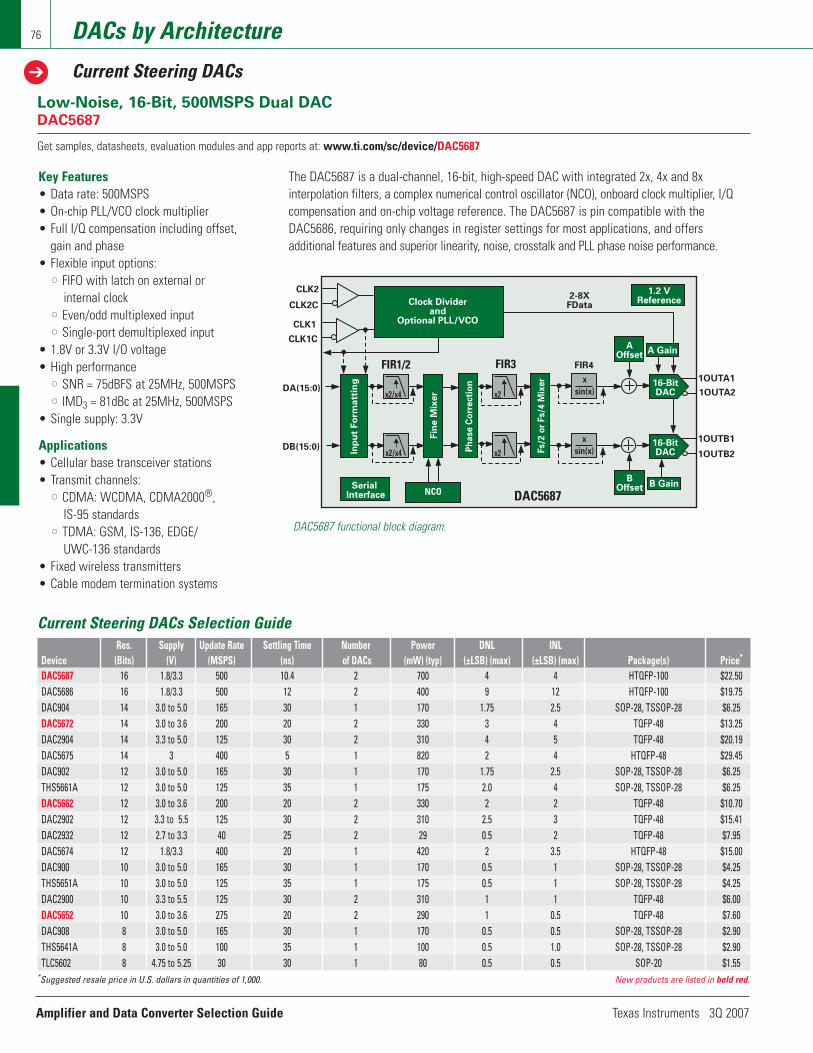
Amplifier and Data Converter Selection Guide Texas Instruments 3Q 2007
DACs by Architecture
Current Steering DACs
76
Clock Dividerand
Optional PLL/VCO
Inp
ut
Fo
rmatt
ing
Serial Interface NCO
x2/x4 x2
AOffset
B Gain
16-BitDAC
FIR1/2 FIR3 FIR4
2-8XFData
1.2 VReference
CLK2
CLK2C
CLK1
CLK1C
DA(15:0)
DB(15:0)
1OUTA1
x2/x4
x2/x4
x2
x2 Fs/2
or
Fs/4
Mix
er x
sin(x)
x
sin(x)
16-BitDAC
A Gain
Fin
e M
ixer 1OUTA2
16-BitDAC
1OUTB1
1OUTB2
BOffset
Ph
ase
Co
rre
cti
on
Low-Noise, 16-Bit, 500MSPS Dual DACDAC5687
Get samples, datasheets, evaluation modules and app reports at: www.ti.com/sc/device/DAC5687
Key Features• Data rate: 500MSPS• On-chip PLL/VCO clock multiplier• Full I/Q compensation including offset,
gain and phase• Flexible input options:
•• FIFO with latch on external or internal clock
•• Even/odd multiplexed input•• Single-port demultiplexed input
• 1.8V or 3.3V I/O voltage• High performance
•• SNR = 75dBFS at 25MHz, 500MSPS•• IMD3 = 81dBc at 25MHz, 500MSPS
• Single supply: 3.3V
Applications• Cellular base transceiver stations• Transmit channels:
•• CDMA: WCDMA, CDMA2000®, IS-95 standards
•• TDMA: GSM, IS-136, EDGE/UWC-136 standards
• Fixed wireless transmitters• Cable modem termination systems
The DAC5687 is a dual-channel, 16-bit, high-speed DAC with integrated 2x, 4x and 8x interpolation filters, a complex numerical control oscillator (NCO), onboard clock multiplier, I/Qcompensation and on-chip voltage reference. The DAC5687 is pin compatible with theDAC5686, requiring only changes in register settings for most applications, and offers additional features and superior linearity, noise, crosstalk and PLL phase noise performance.
DAC5687 functional block diagram.
Current Steering DACs Selection GuideRes. Supply Update Rate Settling Time Number Power DNL INL
Device (Bits) (V) (MSPS) (ns) of DACs (mW) (typ) (±LSB) (max) (±LSB) (max) Package(s) Price*
DAC5687 16 1.8/3.3 500 10.4 2 700 4 4 HTQFP-100 $22.50DAC5686 16 1.8/3.3 500 12 2 400 9 12 HTQFP-100 $19.75DAC904 14 3.0 to 5.0 165 30 1 170 1.75 2.5 SOP-28, TSSOP-28 $6.25DAC5672 14 3.0 to 3.6 200 20 2 330 3 4 TQFP-48 $13.25DAC2904 14 3.3 to 5.0 125 30 2 310 4 5 TQFP-48 $20.19DAC5675 14 3 400 5 1 820 2 4 HTQFP-48 $29.45DAC902 12 3.0 to 5.0 165 30 1 170 1.75 2.5 SOP-28, TSSOP-28 $6.25THS5661A 12 3.0 to 5.0 125 35 1 175 2.0 4 SOP-28, TSSOP-28 $6.25DAC5662 12 3.0 to 3.6 200 20 2 330 2 2 TQFP-48 $10.70DAC2902 12 3.3 to 5.5 125 30 2 310 2.5 3 TQFP-48 $15.41DAC2932 12 2.7 to 3.3 40 25 2 29 0.5 2 TQFP-48 $7.95DAC5674 12 1.8/3.3 400 20 1 420 2 3.5 HTQFP-48 $15.00DAC900 10 3.0 to 5.0 165 30 1 170 0.5 1 SOP-28, TSSOP-28 $4.25THS5651A 10 3.0 to 5.0 125 35 1 175 0.5 1 SOP-28, TSSOP-28 $4.25DAC2900 10 3.3 to 5.5 125 30 2 310 1 1 TQFP-48 $6.00DAC5652 10 3.0 to 3.6 275 20 2 290 1 0.5 TQFP-48 $7.60DAC908 8 3.0 to 5.0 165 30 1 170 0.5 0.5 SOP-28, TSSOP-28 $2.90THS5641A 8 3.0 to 5.0 100 35 1 100 0.5 1.0 SOP-28, TSSOP-28 $2.90TLC5602 8 4.75 to 5.25 30 30 1 80 0.5 0.5 SOP-20 $1.55
*Suggested resale price in U.S. dollars in quantities of 1,000. New products are listed in bold red.
DAC5687
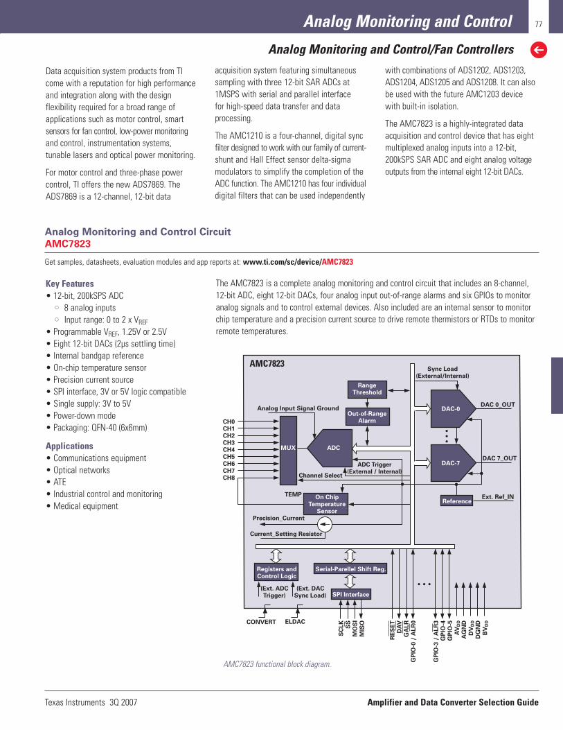
Texas Instruments 3Q 2007 Amplifier and Data Converter Selection Guide
Analog Monitoring and Control
Analog Monitoring and Control/Fan Controllers
77
CH0CH1CH2CH3CH4CH5CH6CH7CH8
Analog Input Signal Ground
Sync Load(External/Internal)
Channel Select
ADC Trigger(External / Internal)
Ext. Ref_IN
DAC 7_OUT
Current_Setting Resistor
Precision_Current
TEMP
DAC 0_OUT
Serial-Parellel Shift Reg.
SPI Interface
CONVERT ELDAC
SC
LK
SS
MO
SI
MIS
O
RE
SE
TD
AV
GA
LR
GP
IO-0
/ A
LR
0
GP
IO-3
/ A
LR
3G
PIO
-4G
PIO
-5A
VD
D
AG
ND
DV
DD
DG
ND
BV
DD
•••
• • •
(Ext. ADCTrigger)
(Ext. DACSync Load)
On ChipTemperature
Sensor
ADCMUX
DAC-0
DAC-7
Out-of-RangeAlarm
RangeThreshold
Registers andControl Logic
Reference
Analog Monitoring and Control Circuit
AMC7823
Get samples, datasheets, evaluation modules and app reports at: www.ti.com/sc/device/AMC7823
AMC7823 functional block diagram.
Key Features• 12-bit, 200kSPS ADC
•• 8 analog inputs•• Input range: 0 to 2 x VREF
• Programmable VREF, 1.25V or 2.5V• Eight 12-bit DACs (2µs settling time)• Internal bandgap reference• On-chip temperature sensor• Precision current source• SPI interface, 3V or 5V logic compatible• Single supply: 3V to 5V• Power-down mode• Packaging: QFN-40 (6x6mm)
Applications• Communications equipment• Optical networks• ATE• Industrial control and monitoring• Medical equipment
The AMC7823 is a complete analog monitoring and control circuit that includes an 8-channel,12-bit ADC, eight 12-bit DACs, four analog input out-of-range alarms and six GPIOs to monitoranalog signals and to control external devices. Also included are an internal sensor to monitorchip temperature and a precision current source to drive remote thermistors or RTDs to monitorremote temperatures.
Data acquisition system products from TIcome with a reputation for high performanceand integration along with the design flexibility required for a broad range of applications such as motor control, smartsensors for fan control, low-power monitoringand control, instrumentation systems, tunable lasers and optical power monitoring.
For motor control and three-phase powercontrol, TI offers the new ADS7869. TheADS7869 is a 12-channel, 12-bit data
acquisition system featuring simultaneoussampling with three 12-bit SAR ADCs at1MSPS with serial and parallel interface for high-speed data transfer and data processing.
The AMC1210 is a four-channel, digital syncfilter designed to work with our family of current-shunt and Hall Effect sensor delta-sigmamodulators to simplify the completion of theADC function. The AMC1210 has four individualdigital filters that can be used independently
with combinations of ADS1202, ADS1203,ADS1204, ADS1205 and ADS1208. It can alsobe used with the future AMC1203 devicewith built-in isolation.
The AMC7823 is a highly-integrated dataacquisition and control device that has eightmultiplexed analog inputs into a 12-bit,200kSPS SAR ADC and eight analog voltageoutputs from the internal eight 12-bit DACs.
AMC7823
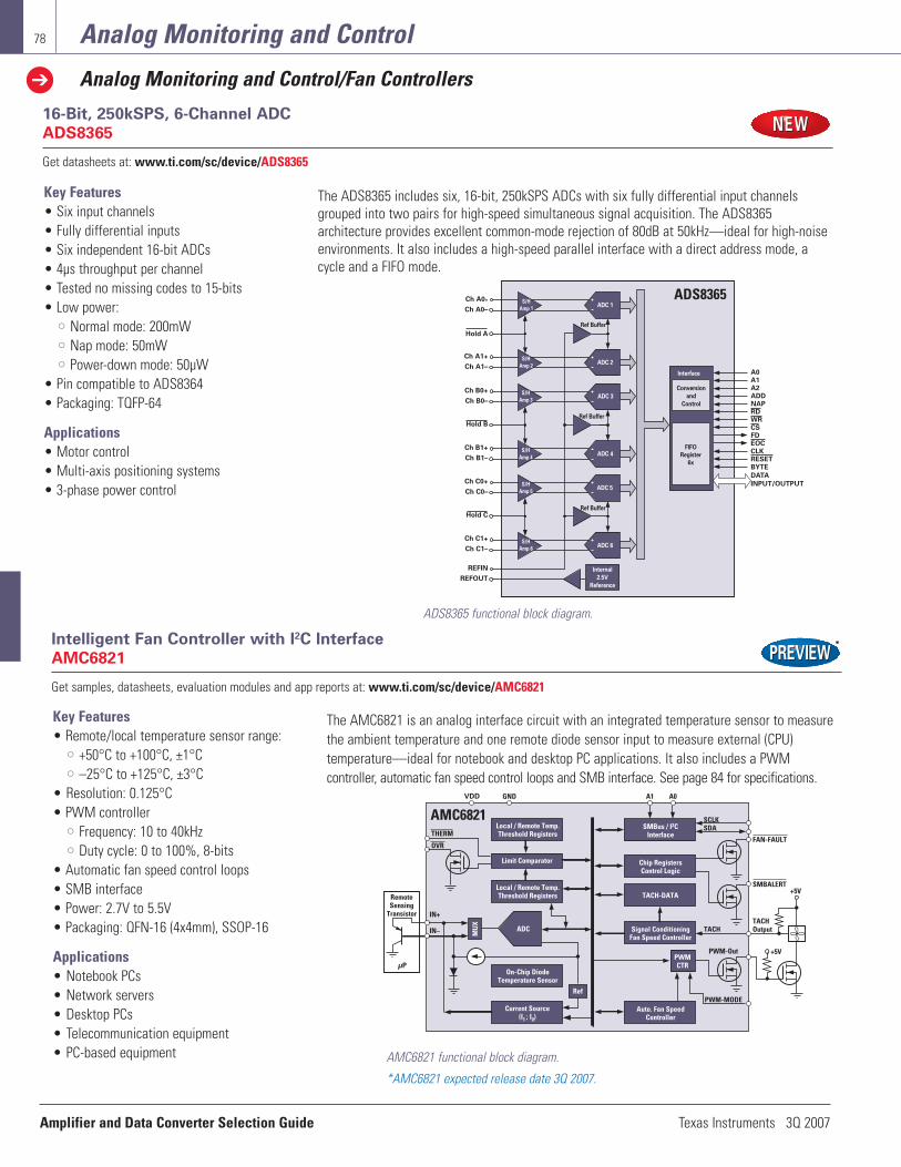
Amplifier and Data Converter Selection Guide Texas Instruments 3Q 2007
Analog Monitoring and Control
Analog Monitoring and Control/Fan Controllers
78
VDD
Intelligent Fan Controller with I2C Interface
AMC6821
Get samples, datasheets, evaluation modules and app reports at: www.ti.com/sc/device/AMC6821
AMC6821 functional block diagram.
*AMC6821 expected release date 3Q 2007.
Key Features• Remote/local temperature sensor range:
•• +50°C to +100°C, ±1°C•• –25°C to +125°C, ±3°C
• Resolution: 0.125°C• PWM controller
•• Frequency: 10 to 40kHz•• Duty cycle: 0 to 100%, 8-bits
• Automatic fan speed control loops• SMB interface• Power: 2.7V to 5.5V• Packaging: QFN-16 (4x4mm), SSOP-16
Applications• Notebook PCs• Network servers• Desktop PCs• Telecommunication equipment• PC-based equipment
The AMC6821 is an analog interface circuit with an integrated temperature sensor to measurethe ambient temperature and one remote diode sensor input to measure external (CPU) temperature—ideal for notebook and desktop PC applications. It also includes a PWM controller, automatic fan speed control loops and SMB interface. See page 84 for specifications.
AMC6821
Interface
Conversion
and
Control
DATA
INPUT/OUTPUT
A0A1A2ADDNAPRDWRCSFDEOCCLKRESETBYTE
ADC 1S/H
Amp 1
Ch A0+
Ch A0–
Hold A
Ch A1+
Ch A1–
Ch B0+
Ch B0–
Hold B
Ch B1+
Ch B1–
Ch C0+
Ch C0–
Hold C
Ch C1+
Ch C1–
REFIN
REFOUT
ADC 2S/H
Amp 2
ADC 3S/H
Amp 3
ADC 4S/H
Amp 4
ADC 5S/H
Amp 5
Ref Buffer
Ref Buffer
Ref Buffer
ADC 6S/H
Amp 6
Internal
2.5V
Reference
FIFO
Register
6x
16-Bit, 250kSPS, 6-Channel ADC
ADS8365
Get datasheets at: www.ti.com/sc/device/ADS8365
ADS8365 functional block diagram.
Key Features• Six input channels• Fully differential inputs• Six independent 16-bit ADCs• 4µs throughput per channel• Tested no missing codes to 15-bits• Low power:
•• Normal mode: 200mW•• Nap mode: 50mW•• Power-down mode: 50µW
• Pin compatible to ADS8364• Packaging: TQFP-64
Applications• Motor control• Multi-axis positioning systems• 3-phase power control
The ADS8365 includes six, 16-bit, 250kSPS ADCs with six fully differential input channelsgrouped into two pairs for high-speed simultaneous signal acquisition. The ADS8365 architecture provides excellent common-mode rejection of 80dB at 50kHz—ideal for high-noiseenvironments. It also includes a high-speed parallel interface with a direct address mode, acycle and a FIFO mode.
ADS8365
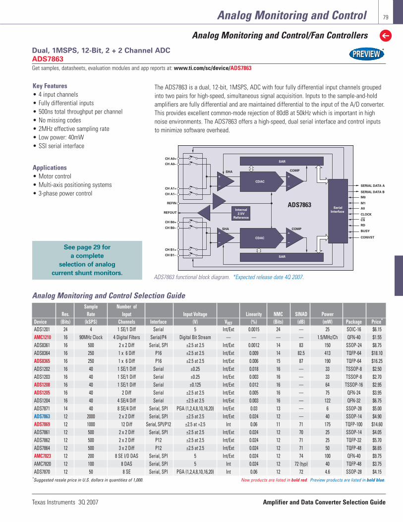
Texas Instruments 3Q 2007 Amplifier and Data Converter Selection Guide
Analog Monitoring and Control
Analog Monitoring and Control/Fan Controllers
79
Analog Monitoring and Control Selection GuideSample Number of
Res. Rate Input Input Voltage Linearity NMC SINAD PowerDevice (Bits) (kSPS) Channels Interface (V) VREF (%) (Bits) (dB) (mW) Package Price*
ADS1201 24 4 1 SE/1 Diff Serial 5 Int/Ext 0.0015 24 — 25 SOIC-16 $6.15 AMC1210 16 90MHz Clock 4 Digital Filters Serial/P4 Digital Bit Stream — — — — 1.5/MHz/Ch QFN-40 $1.55 ADS8361 16 500 2 x 2 Diff Serial, SPI ±2.5 at 2.5 Int/Ext 0.0012 14 83 150 SSOP-24 $8.75 ADS8364 16 250 1 x 6 Diff P16 ±2.5 at 2.5 Int/Ext 0.009 14 82.5 413 TQFP-64 $18.10 ADS8365 16 250 1 x 6 Diff P16 ±2.5 at 2.5 Int/Ext 0.006 15 87 190 TQFP-64 $16.25 ADS1202 16 40 1 SE/1 Diff Serial ±0.25 Int/Ext 0.018 16 — 33 TSSOP-8 $2.50 ADS1203 16 40 1 SE/1 Diff Serial ±0.25 Int/Ext 0.003 16 — 33 TSSOP-8 $2.70 ADS1208 16 40 1 SE/1 Diff Serial ±0.125 Int/Ext 0.012 16 — 64 TSSOP-16 $2.95 ADS1205 16 40 2 Diff Serial ±2.5 at 2.5 Int/Ext 0.005 16 — 75 QFN-24 $3.95 ADS1204 16 40 4 SE/4 Diff Serial ±2.5 at 2.5 Int/Ext 0.003 16 — 122 QFN-32 $6.75 ADS7871 14 40 8 SE/4 Diff Serial, SPI PGA (1,2,4,8,10,16,20) Int/Ext 0.03 13 — 6 SSOP-28 $5.00 ADS7863 12 2000 2 x 2 Diff Serial, SPI ±2.5 at 2.5 Int/Ext 0.024 12 — 40 SSOP-14 $4.90ADS7869 12 1000 12 Diff Serial, SPI/P12 ±2.5 at +2.5 Int 0.06 11 71 175 TQFP-100 $14.60 ADS7861 12 500 2 x 2 Diff Serial, SPI ±2.5 at 2.5 Int/Ext 0.024 12 70 25 SSOP-14 $4.05 ADS7862 12 500 2 x 2 Diff P12 ±2.5 at 2.5 Int/Ext 0.024 12 71 25 TQFP-32 $5.70 ADS7864 12 500 3 x 2 Diff P12 ±2.5 at 2.5 Int/Ext 0.024 12 71 50 TQFP-48 $6.65 AMC7823 12 200 8 SE I/O DAS Serial, SPI 5 Int/Ext 0.024 12 74 100 QFN-40 $9.75 AMC7820 12 100 8 DAS Serial, SPI 5 Int 0.024 12 72 (typ) 40 TQFP-48 $3.75 ADS7870 12 50 8 SE Serial, SPI PGA (1,2,4,8,10,16,20) Int 0.06 12 72 4.6 SSOP-28 $4.15
*Suggested resale price in U.S. dollars in quantities of 1,000. New products are listed in bold red. Preview products are listed in bold blue.
CH A0+
CH A0–
CH A1+
CH A1–
SERIAL DATA A
SERIAL DATA B
M0
A0
CLOCK
CS
RD
BUSY
CONVST
M1
CH B0+
CH B0–
CH B1+
CH B1– SAR
Serial
Interface
COMP
SAR
SHA
CDAC
Internal
2.5V
Reference
SHA COMP
CDAC
REFIN
REFOUT
Dual, 1MSPS, 12-Bit, 2 + 2 Channel ADC
ADS7863
Get samples, datasheets, evaluation modules and app reports at: www.ti.com/sc/device/ADS7863
ADS7863 functional block diagram. *Expected release date 4Q 2007.
Key Features• 4 input channels• Fully differential inputs• 500ns total throughput per channel• No missing codes• 2MHz effective sampling rate• Low power: 40mW• SSI serial interface
Applications• Motor control• Multi-axis positioning systems• 3-phase power control
ADS7863
See page 29 for
a complete
selection of analog
current shunt monitors.
The ADS7863 is a dual, 12-bit, 1MSPS, ADC with four fully differential input channels groupedinto two pairs for high-speed, simultaneous signal acquisition. Inputs to the sample-and-holdamplifiers are fully differential and are maintained differential to the input of the A/D converter.This provides excellent common-mode rejection of 80dB at 50kHz which is important in highnoise environments. The ADS7863 offers a high-speed, dual serial interface and control inputsto minimize software overhead.
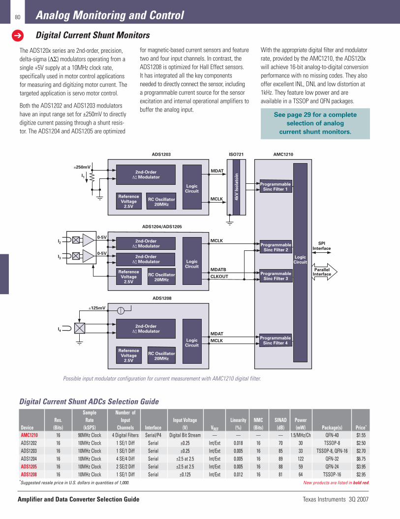
Amplifier and Data Converter Selection Guide Texas Instruments 3Q 2007
80 Analog Monitoring and Control
Digital Current Shunt Monitors
ReferenceVoltage
2.5V
2nd-Order∆∑ Modulator
RC Oscillator20MHz
ProgrammableSinc Filter 1
LogicCircuit
LogicCircuit
4k
V I
so
lato
in
MDAT
ADS1203 ISO721 AMC1210
ADS1204/ADS1205
SPIInterface
ParallelInterface
MCLK
I1
I2
I3
MCLK0-5V
±250mV
0-5V
±125mV
MDATB
CLKOUT
ReferenceVoltage
2.5V
2nd-Order∆∑ Modulator
RC Oscillator20MHz
LogicCircuit
ADS1208
ReferenceVoltage
2.5V
2nd-Order∆∑ Modulator
RC Oscillator20MHz
LogicCircuit
MDAT
MCLK
2nd-Order∆∑ Modulator
I4
ProgrammableSinc Filter 2
ProgrammableSinc Filter 3
ProgrammableSinc Filter 4
The ADS120x series are 2nd-order, precision, delta-sigma (∆Σ) modulators operating from a single +5V supply at a 10MHz clock rate,specifically used in motor control applicationsfor measuring and digitizing motor current. Thetargeted application is servo motor control.
Both the ADS1202 and ADS1203 modulatorshave an input range set for ±250mV to directlydigitize current passing through a shunt resis-tor. The ADS1204 and ADS1205 are optimized
for magnetic-based current sensors and featuretwo and four input channels. In contrast, theADS1208 is optimized for Hall Effect sensors. It has integrated all the key components needed to directly connect the sensor, includinga programmable current source for the sensorexcitation and internal operational amplifiers tobuffer the analog input.
With the appropriate digital filter and modulatorrate, provided by the AMC1210, the ADS120xwill achieve 16-bit analog-to-digital conversionperformance with no missing codes. They alsooffer excellent INL, DNL and low distortion at1kHz. They feature low power and are available in a TSSOP and QFN packages.
See page 29 for a complete
selection of analog
current shunt monitors.
Digital Current Shunt ADCs Selection GuideSample Number of
Res. Rate Input Input Voltage Linearity NMC SINAD PowerDevice (Bits) (kSPS) Channels Interface (V) VREF (%) (Bits) (dB) (mW) Package(s) Price*
AMC1210 16 90MHz Clock 4 Digital Filters Serial/P4 Digital Bit Stream — — — — 1.5/MHz/Ch QFN-40 $1.55 ADS1202 16 10MHz Clock 1 SE/1 Diff Serial ±0.25 Int/Ext 0.018 16 70 30 TSSOP-8 $2.50 ADS1203 16 10MHz Clock 1 SE/1 Diff Serial ±0.25 Int/Ext 0.005 16 85 33 TSSOP-8, QFN-16 $2.70 ADS1204 16 10MHz Clock 4 SE/4 Diff Serial ±2.5 at 2.5 Int/Ext 0.005 16 89 122 QFN-32 $6.75 ADS1205 16 10MHz Clock 2 SE/2 Diff Serial ±2.5 at 2.5 Int/Ext 0.005 16 88 59 QFN-24 $3.95 ADS1208 16 10MHz Clock 1 SE/1 Diff Serial ±0.125 Int/Ext 0.012 16 81 64 TSSOP-16 $2.95
*Suggested resale price in U.S. dollars in quantities of 1,000. New products are listed in bold red.
Possible input modulator configuration for current measurement with AMC1210 digital filter.
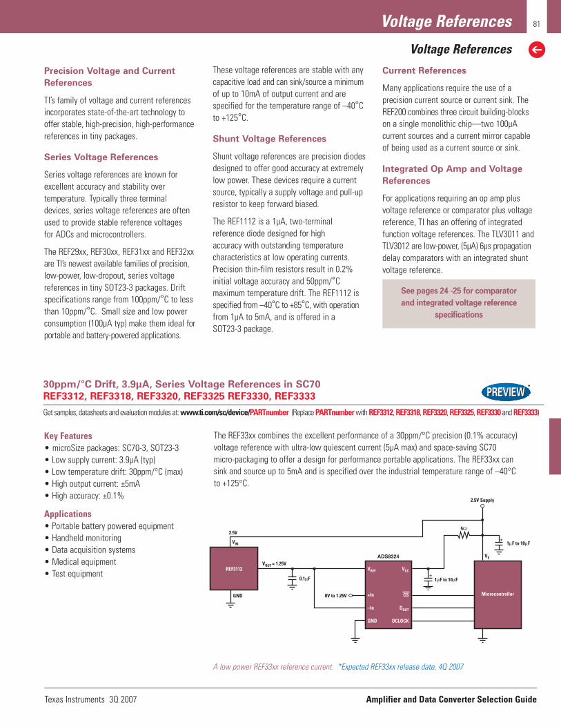
Texas Instruments 3Q 2007 Amplifier and Data Converter Selection Guide
Voltage References
Voltage References
81
Precision Voltage and Current
References
TI’s family of voltage and current referencesincorporates state-of-the-art technology tooffer stable, high-precision, high-performancereferences in tiny packages.
Series Voltage References
Series voltage references are known forexcellent accuracy and stability over temperature. Typically three terminaldevices, series voltage references are oftenused to provide stable reference voltages for ADCs and microcontrollers.
The REF29xx, REF30xx, REF31xx and REF32xxare TI’s newest available families of precision,low-power, low-dropout, series voltage references in tiny SOT23-3 packages. Driftspecifications range from 100ppm/°C to lessthan 10ppm/°C. Small size and low powerconsumption (100µA typ) make them ideal forportable and battery-powered applications.
Current References
Many applications require the use of a precision current source or current sink. TheREF200 combines three circuit building-blockson a single monolithic chip—two 100µA current sources and a current mirror capableof being used as a current source or sink.
Integrated Op Amp and Voltage
References
For applications requiring an op amp plusvoltage reference or comparator plus voltagereference, TI has an offering of integratedfunction voltage references. The TLV3011 andTLV3012 are low-power, (5µA) 6µs propagationdelay comparators with an integrated shuntvoltage reference.
See pages 24 -25 for comparator
and integrated voltage reference
specifications
These voltage references are stable with anycapacitive load and can sink/source a minimumof up to 10mA of output current and arespecified for the temperature range of –40°Cto +125°C.
Shunt Voltage References
Shunt voltage references are precision diodesdesigned to offer good accuracy at extremelylow power. These devices require a currentsource, typically a supply voltage and pull-upresistor to keep forward biased.
The REF1112 is a 1µA, two-terminal reference diode designed for high accuracy with outstanding temperature characteristics at low operating currents.Precision thin-film resistors result in 0.2% initial voltage accuracy and 50ppm/°C maximum temperature drift. The REF1112 isspecified from –40°C to +85°C, with operationfrom 1µA to 5mA, and is offered in a SOT23-3 package.
ADS8324
VCC
CS
DOUT
DCLOCK
VREF
+In
–In
GND
+
+
5Ω
1µF to 10µF
1µF to 10µF
0.1µF
0V to 1.25V Microcontroller
2.5V Supply
REF3112
GND
VIN
2.5V
VOUT = 1.25V
VS
30ppm/°C Drift, 3.9µA, Series Voltage References in SC70
REF3312, REF3318, REF3320, REF3325 REF3330, REF3333
Get samples, datasheets and evaluation modules at: www.ti.com/sc/device/PARTnumber (Replace PARTnumber with REF3312, REF3318, REF3320, REF3325, REF3330 and REF3333)
A low power REF33xx reference current. *Expected REF33xx release date, 4Q 2007
Key Features• microSize packages: SC70-3, SOT23-3• Low supply current: 3.9µA (typ)• Low temperature drift: 30ppm/°C (max)• High output current: ±5mA• High accuracy: ±0.1%
Applications• Portable battery powered equipment• Handheld monitoring• Data acquisition systems• Medical equipment• Test equipment
The REF33xx combines the excellent performance of a 30ppm/°C precision (0.1% accuracy) voltage reference with ultra-low quiescent current (5µA max) and space-saving SC70 micro-packaging to offer a design for performance portable applications. The REF33xx can sink and source up to 5mA and is specified over the industrial temperature range of –40°C to +125°C.
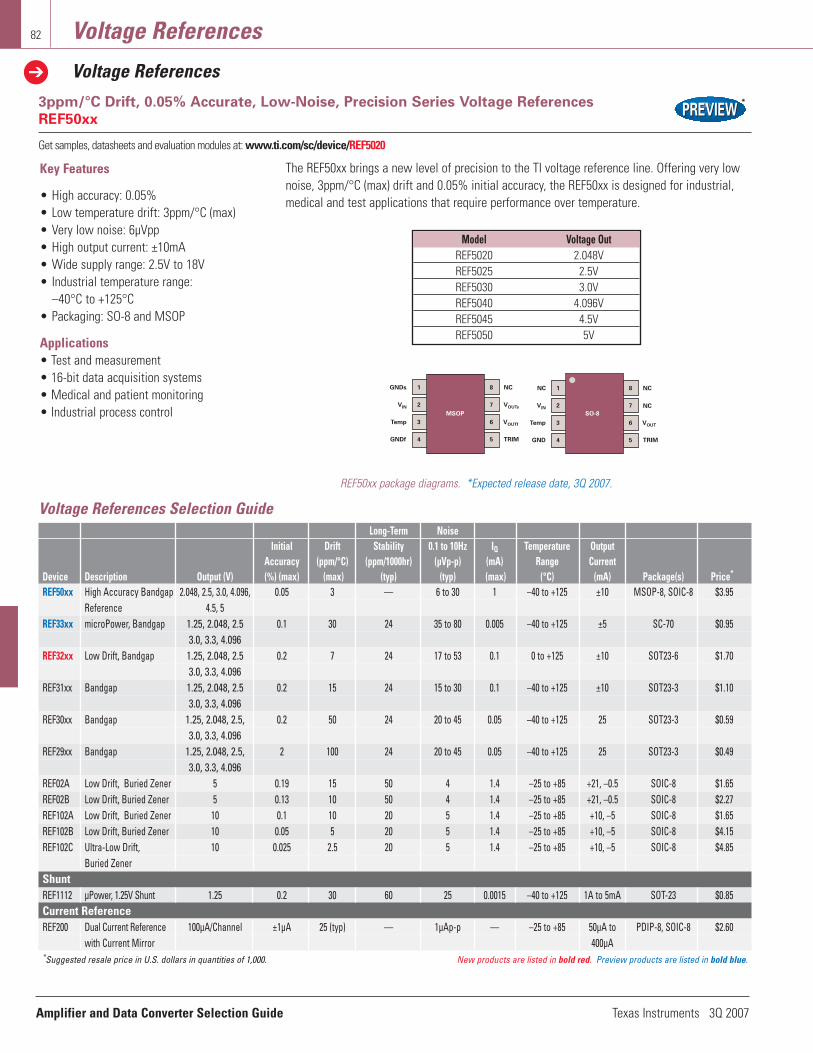
Amplifier and Data Converter Selection Guide Texas Instruments 3Q 2007
Voltage References
Voltage References
82
SO-8
1
2
3
4
1GNDs
MSOP
2VIN
3Temp
4GNDf
8 NC
7 VOUTs
6 VOUTf
5 TRIM
NC
VIN
Temp
GND
NC
NC
VOUT
TRIM
8
7
6
5
3ppm/°C Drift, 0.05% Accurate, Low-Noise, Precision Series Voltage References
REF50xx
Get samples, datasheets and evaluation modules at: www.ti.com/sc/device/REF5020
REF50xx package diagrams. *Expected release date, 3Q 2007.
Key Features
• High accuracy: 0.05%• Low temperature drift: 3ppm/°C (max)• Very low noise: 6µVpp• High output current: ±10mA• Wide supply range: 2.5V to 18V• Industrial temperature range:
–40°C to +125°C• Packaging: SO-8 and MSOP
Applications• Test and measurement• 16-bit data acquisition systems• Medical and patient monitoring• Industrial process control
The REF50xx brings a new level of precision to the TI voltage reference line. Offering very lownoise, 3ppm/°C (max) drift and 0.05% initial accuracy, the REF50xx is designed for industrial,medical and test applications that require performance over temperature.
Voltage References Selection GuideLong-Term Noise
Initial Drift Stability 0.1 to 10Hz IQ Temperature OutputAccuracy (ppm/°C) (ppm/1000hr) (µVp-p) (mA) Range Current
Device Description Output (V) (%) (max) (max) (typ) (typ) (max) (°C) (mA) Package(s) Price*
REF50xx High Accuracy Bandgap 2.048, 2.5, 3.0, 4.096, 0.05 3 — 6 to 30 1 –40 to +125 ±10 MSOP-8, SOIC-8 $3.95Reference 4.5, 5
REF33xx microPower, Bandgap 1.25, 2.048, 2.5 0.1 30 24 35 to 80 0.005 –40 to +125 ±5 SC-70 $0.953.0, 3.3, 4.096
REF32xx Low Drift, Bandgap 1.25, 2.048, 2.5 0.2 7 24 17 to 53 0.1 0 to +125 ±10 SOT23-6 $1.70 3.0, 3.3, 4.096
REF31xx Bandgap 1.25, 2.048, 2.5 0.2 15 24 15 to 30 0.1 –40 to +125 ±10 SOT23-3 $1.10 3.0, 3.3, 4.096
REF30xx Bandgap 1.25, 2.048, 2.5, 0.2 50 24 20 to 45 0.05 –40 to +125 25 SOT23-3 $0.59 3.0, 3.3, 4.096
REF29xx Bandgap 1.25, 2.048, 2.5, 2 100 24 20 to 45 0.05 –40 to +125 25 SOT23-3 $0.49 3.0, 3.3, 4.096
REF02A Low Drift, Buried Zener 5 0.19 15 50 4 1.4 –25 to +85 +21, –0.5 SOIC-8 $1.65 REF02B Low Drift, Buried Zener 5 0.13 10 50 4 1.4 –25 to +85 +21, –0.5 SOIC-8 $2.27 REF102A Low Drift, Buried Zener 10 0.1 10 20 5 1.4 –25 to +85 +10, –5 SOIC-8 $1.65 REF102B Low Drift, Buried Zener 10 0.05 5 20 5 1.4 –25 to +85 +10, –5 SOIC-8 $4.15 REF102C Ultra-Low Drift, 10 0.025 2.5 20 5 1.4 –25 to +85 +10, –5 SOIC-8 $4.85
Buried ZenerShuntREF1112 µPower, 1.25V Shunt 1.25 0.2 30 60 25 0.0015 –40 to +125 1A to 5mA SOT-23 $0.85 Current ReferenceREF200 Dual Current Reference 100µA/Channel ±1µA 25 (typ) — 1µAp-p — –25 to +85 50µA to PDIP-8, SOIC-8 $2.60
with Current Mirror 400µA*Suggested resale price in U.S. dollars in quantities of 1,000. New products are listed in bold red. Preview products are listed in bold blue.
Model Voltage OutREF5020 2.048VREF5025 2.5VREF5030 3.0VREF5040 4.096VREF5045 4.5VREF5050 5V

Texas Instruments 3Q 2007 Amplifier and Data Converter Selection Guide
Temperature Sensors
Temperature Sensors
83
Digital Temperature Sensors
TI’s high-accuracy, low-power temperature sensors are specified for operation from –40°Cto +125°C and are designed for cost-effectivethermal measurement in a variety of communication, computer, consumer, industrial and instrumentation applications.
These silicon-based temperature sensors aredesigned on a unique topology that offersexcellent accuracy and linearity over temperature. Low power and standard communication protocol pair nicely with low-power microcontrollers and battery-powered designs.
The digital temperature output of the TMP family is created using a high-performance, 12-bit, delta-sigma ADC that outputs temperatures as a digital word. Programmingand communication with the TMP1xx family ofdevices is done via an I2C/2-wire or SPI interface for easy integration into existing digital systems.
Temperature Sensor Core
A typical block diagram of the TMP family ofdigital temperature sensors is shown below.Temperature is sensed through the die flag ofthe lead frame where the temperature sensingelement is the chip itself, ensuring the mostaccurate temperature information of the monitored area and allowing designers torespond quickly to “over” and “under” thermal conditions.
Features of TMP Digital
Temperature Sensors
Several TMP digital sensors offer programmable features, including over- and under-temperature thresholds, alarm functions and temperature resolution. Withextremely low power consumption in active(50µA) and standby (0.1µA) modes, theTMP12x family offers as low as 1.5°C minimum error in a SOT23 package and isan excellent candidate for low-power thermal monitoring applications.
The new TMP105 and TMP106 are theworld’s smallest digital temperature sensors. Available in a tiny 1mm x 1.5mmchipscale package, they use only 50µA ofcurrent and are ideal for portable applications including mobile phones,portable media players, digital still cameras, hard disk drives, laptops, andcomputer accessories. TMP105 has 1.8V to3.0V logic, while TMP106 has 2.7V to 5.5V logic.
1
3
4
8
7
6
5
V+
A1
2A0
A2
DiodeTemp
Sensor
ControlLogic
A/DConverter
SerialInterface
OSCConfig.
and TempRegister
GND
ALERT
SCL
SDA
Temperature
TMP175, TMP75
Typical block diagram of the TMP family of digitaltemperature sensors.
DiodeTemp.
Sensor
DSA/D
Converter
OSC
ControlLogic
SerialInterface
Config.and Temp.Register
Temperature
ALERT
SDA1
3
4
8
6
5GND
V+
A1
SCL2 7
A0
A2
0.5°C, Digital Out Temperature Sensor
TMP275
Get samples, datasheets, evaluation modules and app reports at: www.ti.com/sc/device/TMP275
TMP275 functional block diagram.
Key Features• 8 addresses• Digital output: two-wire serial interface• Resolution: 9- to 12-bits, user-selectable• Accuracy:
±0.5°C (max) from +10°C to +85°C±0.75°C (max) from +0°C to +100°C
• Low quiescent current: 50µA, 0.1µA standby• Wide supply range: 2.7V to 5.5V• No power-up sequence required;
two-wire bus pull-ups can be enabledbefore V+
• Packaging: MSOP-8 and SO-8 packages
Applications• Power-supply temperature monitoring• Computer peripheral terminal protection• Notebook computers• Cell phones• Battery management• Office machines• Thermostat controls• Environmental monitoring and HVAC• Electromechanical device temperature
The TMP275 is a 0.5°C accurate, two-wire, serial output temperature sensor available in anMSOP-8 or an SO-8 package. The TMP275 is capable of reading temperatures with a resolutionof 0.0625°C. The TMP275 is SMBus-compatible and allows up to eight devices on one bus. It isideal for extended temperature measurement in a variety of communication, computer, consumer, environmental, industrial, and instrumentation applications.
The TMP275 is specified for operation over a temperature range of –40°C to +125°C.
TMP275
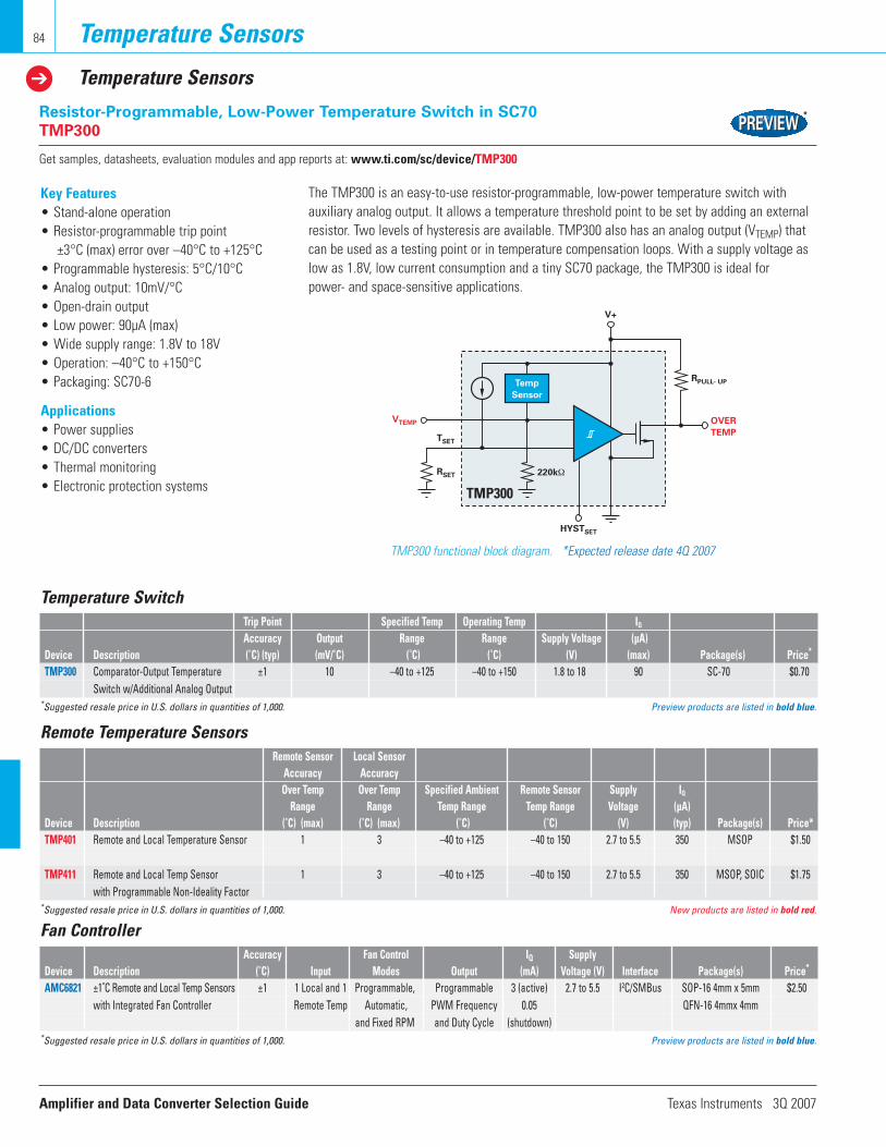
Amplifier and Data Converter Selection Guide Texas Instruments 3Q 2007
Temperature Sensors
Temperature Sensors
84
RPULL- UP
220kΩRSET
TSET
OVER
TEMP
V+
HYSTSET
VTEMP
Temp
Sensor
Resistor-Programmable, Low-Power Temperature Switch in SC70
TMP300
Get samples, datasheets, evaluation modules and app reports at: www.ti.com/sc/device/TMP300
TMP300 functional block diagram. *Expected release date 4Q 2007
Key Features• Stand-alone operation• Resistor-programmable trip point
±3°C (max) error over –40°C to +125°C• Programmable hysteresis: 5°C/10°C• Analog output: 10mV/°C• Open-drain output• Low power: 90µA (max)• Wide supply range: 1.8V to 18V• Operation: –40°C to +150°C • Packaging: SC70-6
Applications• Power supplies• DC/DC converters• Thermal monitoring• Electronic protection systems
The TMP300 is an easy-to-use resistor-programmable, low-power temperature switch with auxiliary analog output. It allows a temperature threshold point to be set by adding an externalresistor. Two levels of hysteresis are available. TMP300 also has an analog output (VTEMP) thatcan be used as a testing point or in temperature compensation loops. With a supply voltage aslow as 1.8V, low current consumption and a tiny SC70 package, the TMP300 is ideal for power- and space-sensitive applications.
TMP300
Temperature SwitchTrip Point Specified Temp Operating Temp IQ
Accuracy Output Range Range Supply Voltage (µA)Device Description (˚C) (typ) (mV/˚C) (˚C) (˚C) (V) (max) Package(s) Price*
TMP300 Comparator-Output Temperature ±1 10 –40 to +125 –40 to +150 1.8 to 18 90 SC-70 $0.70 Switch w/Additional Analog Output
*Suggested resale price in U.S. dollars in quantities of 1,000. Preview products are listed in bold blue.
Fan ControllerAccuracy Fan Control IQ Supply
Device Description (˚C) Input Modes Output (mA) Voltage (V) Interface Package(s) Price*
AMC6821 ±1˚C Remote and Local Temp Sensors ±1 1 Local and 1 Programmable, Programmable 3 (active) 2.7 to 5.5 I2C/SMBus SOP-16 4mm x 5mm $2.50with Integrated Fan Controller Remote Temp Automatic, PWM Frequency 0.05 QFN-16 4mmx 4mm
and Fixed RPM and Duty Cycle (shutdown)*Suggested resale price in U.S. dollars in quantities of 1,000. Preview products are listed in bold blue.
Remote Temperature SensorsRemote Sensor Local Sensor
Accuracy AccuracyOver Temp Over Temp Specified Ambient Remote Sensor Supply IQ
Range Range Temp Range Temp Range Voltage (µA)Device Description (˚C) (max) (˚C) (max) (˚C) (˚C) (V) (typ) Package(s) Price*TMP401 Remote and Local Temperature Sensor 1 3 –40 to +125 –40 to 150 2.7 to 5.5 350 MSOP $1.50
TMP411 Remote and Local Temp Sensor 1 3 –40 to +125 –40 to 150 2.7 to 5.5 350 MSOP, SOIC $1.75with Programmable Non-Ideality Factor
*Suggested resale price in U.S. dollars in quantities of 1,000. New products are listed in bold red.
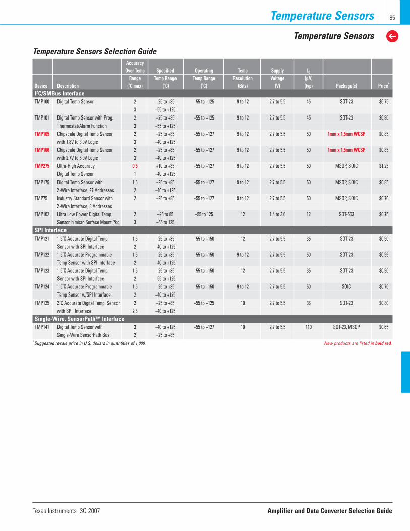
Texas Instruments 3Q 2007 Amplifier and Data Converter Selection Guide
Temperature Sensors
Temperature Sensors
85
Temperature Sensors Selection GuideAccuracyOver Temp Specified Operating Temp Supply IQ
Range Temp Range Temp Range Resolution Voltage (µA)Device Description (˚C max) (˚C) (˚C) (Bits) (V) (typ) Package(s) Price*
I2C/SMBus InterfaceTMP100 Digital Temp Sensor 2 –25 to +85 –55 to +125 9 to 12 2.7 to 5.5 45 SOT-23 $0.75
3 –55 to +125TMP101 Digital Temp Sensor with Prog. 2 –25 to +85 –55 to +125 9 to 12 2.7 to 5.5 45 SOT-23 $0.80
Thermostat/Alarm Function 3 –55 to +125TMP105 Chipscale Digital Temp Sensor 2 –25 to +85 –55 to +127 9 to 12 2.7 to 5.5 50 1mm x 1.5mm WCSP $0.85
with 1.8V to 3.0V Logic 3 –40 to +125TMP106 Chipscale Digital Temp Sensor 2 –25 to +85 –55 to +127 9 to 12 2.7 to 5.5 50 1mm x 1.5mm WCSP $0.85
with 2.7V to 5.0V Logic 3 –40 to +125TMP275 Ultra-High Accuracy 0.5 +10 to +85 –55 to +127 9 to 12 2.7 to 5.5 50 MSOP, SOIC $1.25
Digital Temp Sensor 1 –40 to +125TMP175 Digital Temp Sensor with 1.5 –25 to +85 –55 to +127 9 to 12 2.7 to 5.5 50 MSOP, SOIC $0.85
2-Wire Interface, 27 Addresses 2 –40 to +125TMP75 Industry Standard Sensor with 2 –25 to +85 –55 to +127 9 to 12 2.7 to 5.5 50 MSOP, SOIC $0.70
2-Wire Interface, 8 AddressesTMP102 Ultra Low Power Digital Temp 2 –25 to 85 –55 to 125 12 1.4 to 3.6 12 SOT-563 $0.75
Sensor in micro Surface Mount Pkg. 3 –55 to 125SPI InterfaceTMP121 1.5˚C Accurate Digital Temp 1.5 –25 to +85 –55 to +150 12 2.7 to 5.5 35 SOT-23 $0.90
Sensor with SPI Interface 2 –40 to +125TMP122 1.5˚C Accurate Programmable 1.5 –25 to +85 –55 to +150 9 to 12 2.7 to 5.5 50 SOT-23 $0.99
Temp Sensor with SPI Interface 2 –40 to +125TMP123 1.5˚C Accurate Digital Temp 1.5 –25 to +85 –55 to +150 12 2.7 to 5.5 35 SOT-23 $0.90
Sensor with SPI Interface 2 –55 to +125TMP124 1.5˚C Accurate Programmable 1.5 –25 to +85 –55 to +150 9 to 12 2.7 to 5.5 50 SOIC $0.70
Temp Sensor w/SPI Interface 2 –40 to +125TMP125 2˚C Accurate Digital Temp. Sensor 2 –25 to +85 –55 to +125 10 2.7 to 5.5 36 SOT-23 $0.80
with SPI Interface 2.5 –40 to +125Single-Wire, SensorPath™ InterfaceTMP141 Digital Temp Sensor with 3 –40 to +125 –55 to +127 10 2.7 to 5.5 110 SOT-23, MSOP $0.65
Single-Wire SensorPath Bus 2 –25 to +85*Suggested resale price in U.S. dollars in quantities of 1,000. New products are listed in bold red.
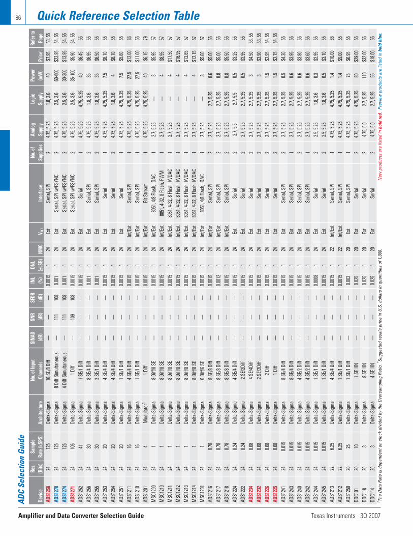
Amplifier and Data Converter Selection Guide Texas Instruments 3Q 2007
Quick Reference Selection Table86AD
C Se
lect
ion
Guid
eRe
s.Sa
mple
No. o
f Inp
utSI
NAD
SNR
SFDR
INL
DNL
No. o
fAn
alog
Logi
cPo
wer
Refe
r to
Devic
e(B
its)
Rate
(kSP
S)
Arch
itect
ure
Chan
nels
(dB)
(dB)
(dB)
(%)
(±LS
B)NM
CV R
EFIn
terfa
ceSu
pplie
sSu
pply
Supp
ly(m
W)
Pric
e*Pa
ge
ADS1
258
2412
5De
lta-S
igma
16 S
E/8 D
iff—
——
0.001
51
24Ex
tSe
rial, S
PI2
4.75,
5.25
1.8, 3
.640
$7.95
53
, 55
ADS1
278
2412
5De
lta-S
igma
8 Diff
Sim
ultan
eous
—11
110
80.0
011
24Ex
tSe
rial, S
PI w
/FSYN
C2
4.75,
5.25
2.5, 3
.660
-600
$23.9
554
, 55
ADS1
274
2412
5De
lta-S
igma
4 Diff
Sim
ultan
eous
—11
110
80.0
011
24Ex
tSe
rial, S
PI w
/FSYN
C2
4.75,
5.25
2.5, 3
.630
-300
$13.9
554
, 55
ADS1
271
2410
5De
lta-S
igma
1 Diff
—10
910
80.0
015
124
Ext
Seria
l, SPI
w/FS
YNC
24.7
5, 5.2
52.5
, 3.6
35-1
00$5
.90
54, 5
5AD
S125
224
41De
lta-S
igma
1 SE/
1 Diff
——
—0.0
015
124
Ext
Seria
l1
4.75,
5.25
4.75,
5.25
40$6
.45
55AD
S125
624
30De
lta-S
igma
8 SE/
4 Diff
——
—0.0
011
24Ex
tSe
rial, S
PI2
4.75,
5.25
1.8, 3
.635
$6.95
55
ADS1
255
2430
Delta
-Sigm
a2 S
E/1 D
iff—
——
0.001
124
Ext
Seria
l, SPI
24.7
5, 5.2
51.8
, 3.6
35$6
.50
55AD
S125
324
20De
lta-S
igma
4 SE/
4 Diff
——
—0.0
015
124
Ext
Seria
l1
4.75,
5.25
4.75,
5.25
7.5$6
.70
55AD
S125
424
20De
lta-S
igma
4 SE/
4 Diff
——
—0.0
015
124
Ext
Seria
l2
4.75,
5.25
1.8, 3
.64
$6.70
55
ADS1
251
2420
Delta
-Sigm
a1 S
E/1 D
iff—
——
0.001
51
24Ex
tSe
rial
14.7
5, 5.2
54.7
5, 5.2
57.5
$5.60
55
ADS1
211
2416
Delta
-Sigm
a4 S
E/4 D
iff—
——
0.001
51
24In
t/Ext
Seria
l, SPI
14.7
5, 5.2
54.7
5, 5.2
527
.5$1
2.00
86AD
S121
024
16De
lta-S
igma
1 SE/
1 Diff
——
—0.0
015
124
Int/E
xtSe
rial, S
PI1
4.75,
5.25
4.75,
5.25
27.5
$11.0
0 55
ADS1
201
244
Mod
ulato
r11 D
iff—
——
0.001
51
24In
t/Ext
Bit S
tream
14.7
5, 5.2
54.7
5, 5.2
540
$6.15
79
MSC
1200
241
Delta
-Sigm
a8 D
iff/8
SE—
——
0.001
51
24In
t/Ext
8051
, 4/8
Flash
, IDAC
12.7
, 5.25
—3
$5.95
57
MSC
1210
241
Delta
-Sigm
a8 D
iff/8
SE—
——
0.001
51
24In
t/Ext
8051
, 4-3
2, 8 F
lash,
PWM
12.7
, 5.25
—4
$8.95
57
MSC
1211
241
Delta
-Sigm
a8 D
iff/8
SE—
——
0.001
51
24In
t/Ext
8051
, 4-3
2, 8 F
lash,
I/VDA
C1
2.7, 5
.25—
4$1
7.50
57M
SC12
1224
1De
lta-S
igma
8 Diff
/8 SE
——
—0.0
015
124
Int/E
xt80
51, 4
-32,
8 Flas
h, I/V
DAC
12.7
, 5.25
—4
$16.9
5 57
MSC
1213
241
Delta
-Sigm
a8 D
iff/8
SE—
——
0.001
51
24In
t/Ext
8051
, 4-3
2, 8 F
lash,
I/VDA
C1
2.7, 5
.25—
4$1
2.65
57M
SC12
1424
1De
lta-S
igma
8 Diff
/8 SE
——
—0.0
015
124
Int/E
xt80
51, 4
-32,
8 Flas
h, I/V
DAC
12.7
, 5.25
—4
$12.1
5 57
MSC
1201
241
Delta
-Sigm
a6 D
iff/6
SE—
——
0.001
51
24In
t/Ext
8051
, 4/8
Flash
, IDAC
12.7
, 5.25
—3
$5.60
57
ADS1
216
240.7
8De
lta-S
igma
8 SE/
8 Diff
——
—0.0
015
124
Int/E
xtSe
rial, S
PI2
2.7, 5
.252.7
, 5.25
0.6$5
.00
55AD
S121
724
0.78
Delta
-Sigm
a8 S
E/8 D
iff—
——
0.001
21
24In
t/Ext
Seria
l, SPI
22.7
, 5.25
2.7, 5
.250.8
$5.00
55
ADS1
218
240.7
8De
lta-S
igma
8 SE/
8 Diff
——
—0.0
015
124
Int/E
xtSe
rial, S
PI2
2.7, 5
.252.7
, 5.25
0.8$5
.50
55AD
S122
424
0.24
Delta
-Sigm
a4 S
E/4 D
iff—
——
0.001
51
24Ex
tSe
rial
22.7
, 5.5
2.7, 5
.50.5
$3.25
55
ADS1
222
240.2
4De
lta-S
igma
2 SE/
2Diff
——
—0.0
015
124
Ext
Seria
l2
2.7, 5
.252.7
, 5.25
0.5$2
.95
55AD
S123
424
0.08
Delta
-Sigm
a4 S
E/4D
iff—
——
0.001
51
24Ex
tSe
rial
22.7
, 5.25
2.7, 5
.253
$4.50
53
, 55
ADS1
232
240.0
8De
lta-S
igma
2 SE/
2Diff
——
—0.0
015
124
Ext
Seria
l2
2.7, 5
.252.7
, 5.25
3$3
.90
53, 5
5AD
S122
624
0.08
Delta
-Sigm
a2 D
iff—
——
0.001
51
24Ex
tSe
rial
22.7
, 5.25
2.7, 5
.251.5
$2.95
54
, 55
ADS1
225
240.0
8De
lta-S
igma
1 Diff
——
—0.0
015
124
Ext
Seria
l2
2.7, 5
.252.7
, 5.25
1.5$2
.75
54, 5
5AD
S124
124
0.015
Delta
-Sigm
a8 S
E/4 D
iff—
——
0.001
51
24Ex
tSe
rial, S
PI2
2.7, 5
.252.7
, 5.25
0.5$4
.20
55AD
S124
324
0.015
Delta
-Sigm
a8 S
E/4 D
iff—
——
0.001
51
24Ex
tSe
rial, S
PI1
2.7, 5
.252.7
, 5.25
0.6$3
.95
55AD
S124
024
0.015
Delta
-Sigm
a4 S
E/2 D
iff—
——
0.001
51
24Ex
tSe
rial, S
PI2
2.7, 5
.252.7
, 5.25
0.6$3
.80
55AD
S124
224
0.015
Delta
-Sigm
a4 S
E/2 D
iff—
——
0.001
51
24Ex
tSe
rial, S
PI1
2.7, 5
.252.7
, 5.25
0.6$3
.60
55AD
S124
424
0.015
Delta
-Sigm
a1 S
E/1 D
iff—
——
0.000
81
24Ex
tSe
rial
22.5
, 5.25
1.8, 3
.60.3
$2.95
55
ADS1
245
240.0
15De
lta-S
igma
1 SE/
1 Diff
——
—0.0
015
124
Ext
Seria
l2
2.5, 5
.251.8
, 3.6
0.5$3
.10
55AD
S121
322
6.25
Delta
-Sigm
a4 S
E/4 D
iff—
——
0.001
51
22In
t/Ext
Seria
l, SPI
14.7
5, 5.2
54.7
5, 5.2
51.4
$10.0
0 86
ADS1
212
226.2
5De
lta-S
igma
1 SE/
1 Diff
——
—0.0
015
122
Int/E
xtSe
rial, S
PI1
4.75,
5.25
4.75,
5.25
1.4$9
.00
55AD
S125
020
25De
lta-S
igma
1 SE/
1 Diff
——
—0.0
031
20Ex
tSe
rial, S
PI1
4.75,
5.25
4.75,
5.25
75$6
.95
55DD
C101
2010
Delta
-Sigm
a1 S
E IIN
——
—0.0
251
20Ex
tSe
rial
24.7
5, 5.2
54.7
5, 5.2
580
$29.0
0 55
DDC1
1820
3De
lta-S
igma
8 SE I
IN—
——
0.025
120
Ext
Seria
l2
4.75,
5.02.7
, 5.25
110
$32.0
0 55
DDC1
1420
3De
lta-S
igma
4 SE I
IN—
——
0.025
120
Ext
Seria
l2
4.75,
5.02.7
, 5.25
55$1
8.00
551 Th
e Da
ta R
ate
is d
epen
dent
on
cloc
k di
vide
d by
the
Over
sam
plin
g Ra
tio. * Su
gges
ted
resa
le p
rice
in U
.S. d
olla
rs in
qua
ntiti
es o
f 1,0
00.
New
pro
duct
s ar
e lis
ted
in b
old
red.
Pre
view
pro
duct
s ar
e lis
ted
in b
old
blue
.
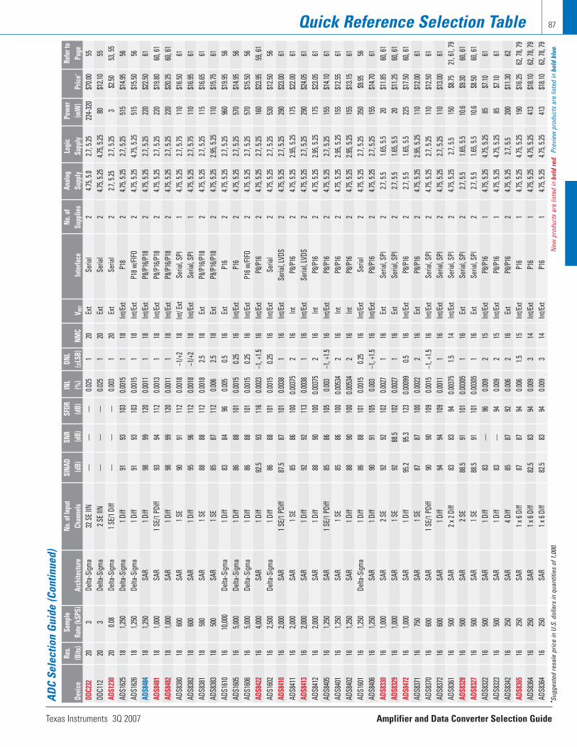
Texas Instruments 3Q 2007 Amplifier and Data Converter Selection Guide
Quick Reference Selection Table 87
Res.
Samp
leNo
. of I
nput
SINA
DSN
RSF
DRIN
LDN
LNo
. of
Anal
ogLo
gic
Pow
erRe
fer t
o De
vice
(Bits
)Ra
te (k
SPS)
Ar
chite
ctur
eCh
anne
ls(d
B)(d
B)(d
B)(%
)(±
LSB)
NMC
V REF
Inte
rface
Supp
lies
Supp
lySu
pply
(mW
)Pr
ice*
Page
DD
C232
203
Delta
-Sigm
a32
SE I
IN—
——
0.025
120
Ext
Seria
l2
4.75,
5.02.7
, 5.25
224-
320
$70.0
0 55
DDC1
1220
3De
lta-S
igma
2 SE I
IN—
——
0.025
120
Ext
Seria
l2
4.75,
5.25
4.75,
5.25
80$1
2.10
55AD
S123
020
0.08
Delta
-Sigm
a1 S
E/1 D
iff—
——
0.003
120
Ext
Seria
l2
2.7, 5
.252.7
, 5.25
3$2
.50
53, 5
5AD
S162
518
1,250
Delta
-Sigm
a1 D
iff91
9310
30.0
015
118
Int/E
xtP1
82
4.75,
5.25
2.7, 5
.2551
5$1
4.95
56AD
S162
618
1,250
Delta
-Sigm
a1 D
iff91
9310
30.0
015
118
Int/E
xtP1
8 w/FI
FO2
4.75,
5.25
4.75,
5.25
515
$15.5
056
ADS8
484
181,2
50SA
R1 D
iff98
9912
00.0
011
118
Int/E
xtP8
/P16
/P18
24.7
5, 5.2
52.7
, 5.25
220
$22.5
0 61
ADS8
481
181,0
00SA
R1 S
E/1 P
Diff
9394
112
0.001
31
18In
t/Ext
P8/P
16/P
182
4.75,
5.25
2.7, 5
.2522
0$1
9.80
60, 6
1AD
S848
218
1,000
SAR
1 Diff
9899
120
0.001
11
18In
t/Ext
P8/P
16/P
182
4.75,
5.25
2.7, 5
.2522
0$2
0.25
60, 6
1AD
S838
018
600
SAR
1 SE
9091
112
0.001
8–1
/+2
18In
t/ Ex
tSe
rial, S
PI1
4.75,
5.25
2.7, 5
.7511
0$1
6.50
61AD
S838
218
600
SAR
1 Diff
9596
112
0.001
8–1
/+2
18In
t/Ext
Seria
l, SPI
14.7
5, 5.2
52.7
, 5.75
110
$16.9
5 61
ADS8
381
1858
0SA
R1 S
E88
8811
20.0
018
2.518
Ext
P8/P
16/P
182
4.75,
5.25
2.7, 5
.2511
5$1
6.65
61AD
S838
318
500
SAR
1 SE
8587
112
0.006
2.518
Ext
P8/P
16/P
182
4.75,
5.25
2.95,
5.25
110
$15.7
5 61
ADS1
610
1610
,000
Delta
-Sigm
a1 D
iff83
8496
0.005
0.516
Ext
P16
24.7
5, 5.2
52.7
, 5.25
960
$19.9
556
ADS1
605
165,0
00De
lta-S
igma
1 Diff
8688
101
0.001
50.2
516
Int/E
xtP1
62
4.75,
5.25
2.7, 5
.2557
0$1
4.95
56AD
S160
616
5,000
Delta
-Sigm
a1 D
iff86
8810
10.0
015
0.25
16In
t/Ext
P16 w
/FIFO
24.7
5, 5.2
52.7
, 5.25
570
$15.5
0 56
ADS8
422
164,0
00SA
R1 D
iff92
.593
116
0.002
3–1
, +1.5
16In
t/Ext
P8/P
162
4.75,
5.25
2.7, 5
.2516
0$2
3.95
59, 6
1AD
S160
216
2,500
Delta
-Sigm
a1 D
iff86
8810
10.0
015
0.25
16In
t/Ext
Seria
l2
4.75,
5.25
2.7, 5
.2553
0$1
2.50
56AD
S841
016
2,000
SAR
1 SE/
1 PDi
ff87
.587
101
0.003
81
16In
t/Ext
Seria
l, LVD
S2
4.75,
5.25
2.7, 5
.2529
0$2
3.00
61AD
S841
116
2,000
SAR
1 SE
8586
100
0.003
752
16In
tP8
/P16
24.7
5, 5.2
52.9
5, 5.2
517
5$2
2.00
61AD
S841
316
2,000
SAR
1 Diff
9292
113
0.003
81
16In
t/Ext
Seria
l, LVD
S2
4.75,
5.25
2.7, 5
.2529
0$2
4.05
61AD
S841
216
2,000
SAR
1 Diff
8890
100
0.003
752
16In
tP8
/P16
24.7
5, 5.2
52.9
5, 5.2
517
5$2
3.05
61AD
S840
516
1,250
SAR
1 SE/
1 PDi
ff85
8610
50.0
03–1
, +1.5
16In
t/Ext
P8/P
162
4.75,
5.25
2.7, 5
.2515
5$1
4.10
61AD
S840
116
1,250
SAR
1 SE
8586
100
0.005
342
16In
tP8
/P16
24.7
5, 5.2
52.9
5, 5.2
515
5$1
2.55
61AD
S840
216
1,250
SAR
1 Diff
8890
100
0.005
342
16In
tP8
/P16
24.7
5, 5.2
52.9
5, 5.2
515
5$1
3.15
61AD
S160
116
1,250
Delta
-Sigm
a1 D
iff86
8810
10.0
015
0.25
16In
t/Ext
Seria
l2
4.75,
5.25
2.7, 5
.2535
0$9
.9556
ADS8
406
161,2
50SA
R1 D
iff90
9110
50.0
03–1
, +1.5
16In
t/Ext
P8/P
162
4.75,
5.25
2.7, 5
.2515
5$1
4.70
61AD
S833
016
1,000
SAR
2 SE
9292
102
0.002
71
16Ex
tSe
rial, S
PI2
2.7, 5
.51.6
5, 5.5
20$1
1.85
60, 6
1AD
S832
916
1,000
SAR
1 SE
9288
.510
20.0
027
116
Ext
Seria
l, SPI
22.7
, 5.5
1.65,
5.520
$11.2
5 60
, 61
ADS8
472
161,0
00SA
R1 D
iff95
.295
.312
30.0
0099
0.516
Int/E
xtP8
/P16
22.7
, 5.5
1.65,
5.522
5$1
7.50
60, 6
1AD
S837
116
750
SAR
1 SE
8787
100
0.002
22
16Ex
tP8
/P16
24.7
5, 5.2
52.9
5, 5.2
511
0$1
2.00
61AD
S837
016
600
SAR
1 SE/
1 PDi
ff90
9010
90.0
015
–1, +
1.516
Int/E
xtSe
rial, S
PI2
4.75,
5.25
2.7, 5
.2511
0$1
2.50
61AD
S837
216
600
SAR
1 Diff
9494
109
0.001
11
16In
t/Ext
Seria
l, SPI
24.7
5, 5.2
52.7
, 5.25
110
$13.0
0 61
ADS8
361
1650
0SA
R2 x
2 Di
ff83
8394
0.003
751.5
14In
t/Ext
Seria
l, SPI
24.7
5, 5.2
52.7
, 5.5
150
$8.75
21
, 61,
79AD
S832
816
500
SAR
2 SE
88.5
9110
10.0
0305
116
Ext
Seria
l, SPI
22.7
, 5.5
1.65,
5.510
.6$9
.30
60, 6
1AD
S832
716
500
SAR
1 SE
88.5
9110
10.0
0305
116
Ext
Seria
l, SPI
22.7
, 5.5
1.65,
5.510
.6$8
.50
60, 6
1AD
S832
216
500
SAR
1 Diff
83—
960.0
092
15In
t/Ext
P8/P
161
4.75,
5.25
4.75,
5.25
85$7
.10
61AD
S832
316
500
SAR
1 Diff
83—
940.0
092
15In
t/Ext
P8/P
161
4.75,
5.25
4.75,
5.25
85$7
.10
61AD
S834
216
250
SAR
4 Diff
8587
920.0
062
16Ex
tP8
/P16
24.7
5, 5.2
52.7
, 5.5
200
$11.3
0 62
ADS8
365
1625
0SA
R1 x
6 Di
ff87
8794
0.006
1.515
Int/E
xtP1
61
4.75,
5.25
4.75,
5.25
190
$16.2
5 62
, 78,
79AD
S836
416
250
SAR
1 x 6
Diff
82.5
8394
0.009
314
Int/E
xtP1
61
4.75,
5.25
4.75,
5.25
413
$18.1
0 62
, 78,
79AD
S836
416
250
SAR
1 x 6
Diff
82.5
8394
0.009
314
Int/E
xtP1
61
4.75,
5.25
4.75,
5.25
413
$18.1
0 62
, 78,
79• Su
gges
ted
resa
le p
rice
in U
.S. d
olla
rs in
qua
ntiti
es o
f 1,0
00.
New
pro
duct
s ar
e lis
ted
in b
old
red.
Pre
view
pro
duct
s ar
e lis
ted
in b
old
blue
.
ADC
Sele
ctio
n Gu
ide
(Con
tinue
d)

Amplifier and Data Converter Selection Guide Texas Instruments 3Q 2007
Quick Reference Selection Table88
Res.
Samp
leNo
. of I
nput
SINA
DSN
RSF
DRIN
LDN
LNo
. of
Anal
ogLo
gic
Pow
erRe
fer t
o De
vice
(Bits
)Ra
te (k
SPS)
Ar
chite
ctur
eCh
anne
ls(d
B)(d
B)(d
B)(%
)(±
LSB)
NMC
V REF
Inte
rface
Supp
lies
Supp
lySu
pply
(mW
)Pr
ice*
Page
AD
S832
616
250
SAR
1 SE/
1 Diff
9191
108
0.002
21
16Ex
tSe
rial, S
PI1
2.7, 5
.252.7
, 5.25
2.25
$5.00
62
ADS8
515
1625
0SA
R1 S
E92
8810
00.0
051
16In
t/Ext
P8/P
161
4.75,
5.25
4.75,
5.25
70$1
0.95
61AD
S850
916
250
SAR
1 SE
8688
100
0.003
116
Int/E
xtSe
rial, S
PI1
4.75,
5.25
4.75,
5.25
70$1
2.95
59, 6
2AD
S850
516
250
SAR
1 SE
8688
100
0.002
21
16In
t/Ext
P8/P
161
4.75,
5.25
4.75,
5.25
70$1
2.95
11, 5
9, 62
ADS7
811
1625
0SA
R1 S
E87
8710
00.0
062
15In
t/Ext
P16
24.7
5, 5.2
54.7
5, 5.2
520
0$3
6.15
62AD
S781
516
250
SAR
1 SE
8484
100
0.006
215
Int/E
xtP1
62
4.75,
5.25
4.75,
5.25
200
$21.3
0 62
ADS8
317
1620
0SA
R1 D
iff88
8810
80.0
022
116
Ext
Seria
l, SPI
12.7
, 5.5
2.7, 5
.55.7
$5.90
62TL
C454
116
200
SAR
1 SE
84.5
8595
0.004
52
16Ex
tSe
rial, S
PI1
4.5, 5
.54.5
, 5.5
17.5
$6.85
62
TLC4
545
1620
0SA
R1 P
Diff
84.5
8595
0.004
52
16Ex
tSe
rial, S
PI1
4.5, 5
.54.5
, 5.5
17.5
$6.85
62
ADS8
344
1610
0SA
R8 S
E/4 D
iff86
—92
0.006
215
Ext
Seria
l, SPI
12.7
, 5.25
2.7, 5
.253.6
$8.00
62
ADS8
345
1610
0SA
R8 S
E/4 D
iff85
—98
0.006
215
Ext
Seria
l, SPI
12.7
, 5.25
2.7, 5
.253.6
$8.00
62
ADS8
341
1610
0SA
R4 S
E/2 D
iff86
—92
0.006
215
Ext
Seria
l, SPI
12.7
, 5.25
2.7, 5
.253.6
$7.40
62
ADS8
343
1610
0SA
R4 S
E/2 D
iff86
—97
0.006
215
Ext
Seria
l, SPI
12.7
, 5.25
2.7, 5
.253.6
$7.45
62
ADS7
805
1610
0SA
R1 S
E86
8694
0.004
51
16In
t/Ext
P8/P
161
4.75,
5.25
4.75,
5.25
81.5
$25.0
062
AD
S780
916
100
SAR
1 SE
8888
100
0.004
51
16In
t/Ext
Seria
l, SPI
14.7
5, 5.2
54.7
5, 5.2
581
.5$2
5.00
62AD
S832
016
100
SAR
1 SE/
1 Diff
8492
860.0
122
15Ex
tSe
rial, S
PI1
2.7, 5
.252.7
, 5.25
1.95
$5.15
62
ADS8
321
1610
0SA
R1 P
Diff
8487
860.0
122
15Ex
tSe
rial, S
PI1
4.75,
5.25
4.75,
5.25
5.5$5
.1562
AD
S832
516
100
SAR
1 SE/
1 Diff
9191
108
0.006
216
Ext
Seria
l, SPI
12.7
, 5.25
2.7, 5
.252.2
5$5
.9062
AD
S120
416
40M
odula
tor1
4 SE/
4 Diff
——
—0.0
031
16In
t/Ext
Bit S
tream
14.7
5, 5.2
54.7
5, 5.2
560
$6.75
77, 7
9, 80
AD
S782
516
40SA
R4 S
E83
8690
0.003
116
Int/E
xtSe
rial, S
PI/P
81
4.75,
5.25
4.75,
5.25
50$2
9.55
62
ADS1
205
1640
Mod
ulato
r12 S
E/2 D
iff88
.288
.998
0.005
116
Int/E
xtBi
t Stre
am1
4.5, 5
.52.7
, 5.5
75$3
.9577
, 79,
80
ADS1
208
1640
Mod
ulato
r11 S
E/1 D
iff81
.582
930.0
121
16In
t/Ext
Bit S
tream
24.5
, 5.5
2.7, 5
.564
$2.95
77
, 79,
80AD
S120
216
40M
odula
tor1
1 SE/
1 Diff
——
—0.0
181
16In
t/Ext
Bit S
tream
14.7
5, 5.2
54.7
5, 5.2
530
$2.50
77, 7
9, 80
AD
S120
316
40M
odula
tor1
1 SE/
1 Diff
——
—0.0
031
16In
t/Ext
Bit S
tream
14.7
5, 5.2
54.7
5, 5.2
530
$2.70
77
, 79,
80AD
S850
716
40SA
R1 S
E89
.992
102
0.002
21.5
16In
t/Ext
Seria
l, SPI
/P8
14.7
5, 5.2
54.7
5, 5.2
528
$13.0
059
, 62
ADS7
807
1640
SAR
1 SE
8888
100
0.002
21.5
16In
t/Ext
Seria
l, SPI
/P8
14.7
5, 5.2
54.7
5, 5.2
528
$32.3
062
AD
S851
316
40SA
R1 S
E89
.992
102
0.003
116
Int/E
xtSe
rial, S
PI1
4.75,
5.25
4.75,
5.25
30$1
2.00
59, 6
2AD
S781
316
40SA
R1 S
E89
8910
20.0
031
16In
t/Ext
Seria
l, SPI
14.7
5, 5.2
54.7
5, 5.2
535
$24.7
0 62
MSC
1202
161
Delta
-Sigm
a6 D
iff/6
SE—
——
0.001
51
24In
t/Ext
8051
, 4/8
Flash
, IDAC
12.7
, 5.25
—3
$4.60
57
ADS1
112
160.2
4De
lta-S
igma
3 SE/
2 Diff
——
—0.0
11
16In
tSe
rial, I
2 C1
2.7, 5
.52.7
, 5.5
0.7$2
.65
55AD
S111
016
0.24
Delta
-Sigm
a1 S
E/1 D
iff—
——
0.01
116
Int
Seria
l, I2 C
12.7
, 5.5
2.7, 5
.50.7
$1.95
55
ADS1
100
160.1
28De
lta-S
igma
1 SE/
1 Diff
——
—0.0
125
116
Ext
Seria
l, I2 C
12.7
, 5.5
2.7, 5
.50.3
$1.80
55
ADS5
547
1421
0,000
Pipe
line
1 Diff
—73
.385
—0.5
14In
t/Ext
DDR
LVDS
/CM
OS, P
81
3.0, 3
.63.0
, 3.6
1230
$82.5
0 66
, 67
ADS5
546
1419
0,000
Pipe
line
1 Diff
—73
.284
0.018
0.514
Int/E
xtDD
R LV
DS/C
MOS
, P8
13.0
, 3.6
3.0, 3
.612
30$7
2.50
66, 6
7AD
S554
514
170,0
00Pi
pelin
e1 D
iff—
73.5
850.0
180.5
14In
t/Ext
DDR
LVDS
/CM
OS, P
81
3.0, 3
.63.0
, 3.6
1230
$62.5
066
, 67
ADS5
500
1412
5,000
Pipe
line
1 Diff
7070
.582
0.03
–0.9/
+1.1
14In
tP1
41
3.0, 3
.63.0
, 3.6
780
$95.0
067
AD
S550
0-EP
1412
5,000
Pipe
line
1 Diff
7070
.582
0.03
–0.9/
+1.1
14In
tP1
41
3.0, 3
.63.0
, 3.6
780
$190
.0088
AD
S624
514
125,0
00Pi
pelin
e2 D
iff72
.373
.283
0.03
2.514
Int/E
xtSe
rial, L
VDS
13.0
, 3.6
3.0, 3
.610
00$7
3.50
67AD
S644
514
125,0
00Pi
pelin
e4 D
iff72
.373
.283
0.03
2.514
Int/E
xtSe
rial, L
VDS
13.0
, 3.6
3.0, 3
.610
00$1
32.30
65, 6
7AD
S554
114
105,0
00Pi
pelin
e1 D
iff—
7182
——
14In
tP1
41
3.0, 3
.63.3
710
$75.0
067
1 Th
e Da
ta R
ate
is d
epen
dent
on
cloc
k di
vide
d by
the
Over
sam
plin
g Ra
tio.
* Sugg
este
d re
sale
pric
e in
U.S
. dol
lars
in q
uant
ities
of 1
,000
. N
ew p
rodu
cts
are
liste
d in
bol
d re
d. P
revi
ew p
rodu
cts
are
liste
d in
bol
d bl
ue.
ADC
Sele
ctio
n Gu
ide
(Con
tinue
d)
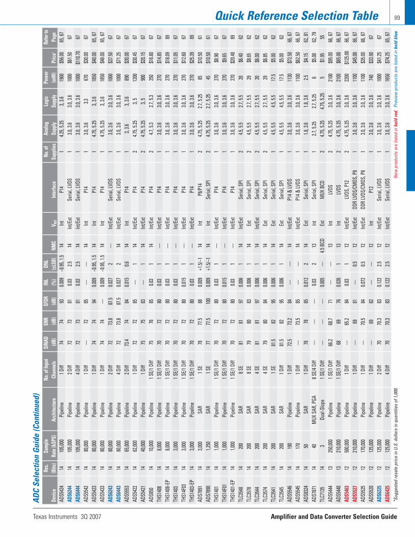
Texas Instruments 3Q 2007 Amplifier and Data Converter Selection Guide
Quick Reference Selection Table 89
Res.
Samp
leNo
. of I
nput
SINA
DSN
RSF
DRIN
LDN
LNo
. of
Anal
ogLo
gic
Pow
erRe
fer t
o De
vice
(Bits
)Ra
te (k
SPS)
Ar
chite
ctur
eCh
anne
ls(d
B)(d
B)(d
B)(%
)(±
LSB)
NMC
V REF
Inte
rface
Supp
lies
Supp
lySu
pply
(mW
)Pr
ice*
Page
AD
S542
414
105,0
00Pi
pelin
e1 D
iff74
7493
0.009
–0.95
, 1.5
14In
tP1
41
4.25,
5.25
3, 3.6
1900
$56.0
065
, 67
ADS6
244
1410
5,000
Pipe
line
2 Diff
7273
810.0
32.5
14In
t/Ext
Seria
l, LVD
S1
3.0, 3
.63.0
, 3.6
1000
$61.5
067
ADS6
444
1410
5,000
Pipe
line
4 Diff
7273
810.0
32.5
14In
t/Ext
Seria
l, LVD
S1
3.0, 3
.63.0
, 3.6
1000
$110
.7067
ADS5
542
1480
,000
Pipe
line
1 Diff
—72
85—
—14
Int
P14
13.0
, 3.6
3.367
0$3
0.00
67
ADS5
423
1480
,000
Pipe
line
1 Diff
7474
940.0
09–0
.95, 1
.514
Int
P14
14.7
5, 5.2
53,
3.618
50$4
0.00
65, 6
7 AD
S543
314
80,00
0Pi
pelin
e1 D
iff74
74—
0.009
–0.95
, 1.5
14In
tP1
41
4.75,
5.25
3, 3.6
1850
$48.0
0 65
, 67
ADS6
243
1480
,000
Pipe
line
2 Diff
7273
.887
.50.0
272
—In
t/Ext
Seria
l, LVD
S1
3.0, 3
.63.0
, 3.6
1000
$37.5
067
ADS6
443
1480
,000
Pipe
line
4 Diff
7273
.887
.50.0
272
14In
t/Ext
Seria
l, LVD
S1
3.0, 3
.63.0
, 3.6
1000
$71.2
567
ADS5
553
1465
,000
Pipe
line
2 Diff
73.4
7484
0.015
0.614
Int
P14
13,
3.63,
3.689
0$3
0.00
67AD
S542
214
62,00
0Pi
pelin
e1 D
iff72
7285
—1
14In
t/Ext
P14
24.7
5, 5.2
53,
512
00$3
0.45
67
ADS5
421
1440
,000
Pipe
line
1 Diff
7575
83—
114
Int/E
xtP1
42
4.75,
5.25
3, 5
900
$20.1
567
AD
S850
1410
,000
Pipe
line
1 SE/
1 Diff
7576
850.0
31
14In
t/Ext
P14
24.7
, 5.3
2.7, 5
.325
0$1
6.80
67TH
S140
814
8,000
Pipe
line
1 SE/
1 Diff
7072
800.0
31
—In
t/Ext
P14
13.0
, 3.6
3.0, 3
.627
0$1
4.85
67TH
S140
8-EP
148,0
00Pi
pelin
e1 S
E/1 D
iff70
7280
0.03
1—
Int/E
xtP1
41
3.0, 3
.63.0
, 3.6
270
$18.0
989
TH
S140
314
3,000
Pipe
line
1 SE/
1 Diff
7072
800.0
31
—In
t/Ext
P14
13.0
, 3.6
3.0, 3
.627
0$1
1.05
67TH
S14F
0314
3,000
Pipe
line
1 SE/
1 Diff
7072
800.0
151
—In
t/Ext
P14
13.0
, 3.6
3.0, 3
.627
0$1
2.60
67TH
S140
3-EP
143,0
00Pi
pelin
e1 S
E/1 D
iff70
7280
0.03
1—
Int/E
xtP1
41
3.0, 3
.63.0
, 3.6
270
$25.3
9 89
ADS7
891
143,0
00SA
R1 S
E78
77.5
880.0
09+1
.5/–1
14In
tP8
/P14
24.7
5, 5.2
52.7
, 5.25
85$1
0.50
61
ADS7
890
141,2
50SA
R1 S
E77
77.5
100
0.009
+1.5/
–114
Int
Seria
l, SPI
24.7
5, 5.2
52.7
, 5.25
45$1
0.50
61TH
S140
114
1,000
Pipe
line
1 SE/
1 Diff
7072
800.0
31
—In
t/Ext
P14
13.0
, 3.6
3.0, 3
.627
0$8
.90
67TH
S14F
0114
1,000
Pipe
line
1 SE/
1 Diff
7072
800.0
151
—In
t/Ext
P14
13.0
, 3.6
3.0, 3
.627
0$9
.65
67TH
S140
1-EP
141,0
00Pi
pelin
e1 S
E/1 D
iff70
7280
0.03
1—
Int/E
xtP1
41
3.0, 3
.63.0
, 3.6
270
$20.4
889
TL
C354
814
200
SAR
8 SE
8181
970.0
061
14In
t/Ext
Seria
l, SPI
24.5
, 5.5
2.7, 5
.520
$6.40
62
TLC3
578
1420
0SA
R8 S
E79
8083
0.006
114
Ext
Seria
l, SPI
24.5
, 5.5
2.7, 5
.529
$8.65
62
TLC3
544
1420
0SA
R4 S
E81
8197
0.006
114
Int/E
xtSe
rial, S
PI2
4.5, 5
.52.7
, 5.5
20$6
.0062
TL
C357
414
200
SAR
4 SE
7980
840.0
061
14Ex
tSe
rial, S
PI2
4.5, 5
.52.7
, 5.5
29$6
.85
62TL
C354
114
200
SAR
1 SE
81.5
8295
0.006
114
Ext
Seria
l, SPI
14.5
, 5.5
4.5, 5
.517
.5$5
.00
62TL
C354
514
200
SAR
1 Diff
81.5
8295
0.006
114
Ext
Seria
l, SPI
14.5
, 5.5
4.5, 5
.517
.5$5
.00
62AD
S554
614
190
Pipe
line
1 Diff
72.5
73.2
84—
—14
Int/E
xtP1
4 & LV
DS1
3.0, 3
.63.0
, 3.6
1130
$72.5
0 66
, 67
ADS5
545
1417
0Pi
pelin
e1 D
iff—
73.5
85—
—14
Int/E
xtP1
4 & LV
DS1
3.0, 3
.63.0
, 3.6
1100
$62.5
066
, 67
ADS8
324
1450
SAR
1 Diff
7878
850.0
122
14Ex
tSe
rial, S
PI1
1.8, 3
.61.8
, 3.6
2.5$4
.15
62, 8
1AD
S787
114
40M
UX S
AR, P
GA8 S
E/4 D
iff—
——
0.03
213
Int
Seria
l, SPI
12.7
, 5.25
2.7, 5
.256
$5.00
62, 7
9 TL
C713
514
3Du
al-Sl
ope
1 SE/
1 Diff
——
—0.0
05—
4.5 B
CDEx
tM
UX B
CD2
4.75,
5.25
4.75,
5.25
5$1
.95
55AD
S544
413
250,0
00Pi
pelin
e1 S
E/1 D
iff66
.268
.771
——
13In
tLV
DS2
4.75,
5.25
3.0, 3
.621
00$9
5.00
66, 6
7AD
S544
013
210,0
00Pi
pelin
e1 S
E/1 D
iff68
6976
0.026
113
Int
LVDS
24.7
5, 5.2
53.0
, 3.6
2100
$65.0
066
, 67
ADS5
463
1250
0,000
Pipe
line
1 Diff
—65
.284
0.03
112
Int/E
xtLV
DS, P
122
4.75,
5.25
3.0, 3
.622
00$1
25.00
66, 6
7 AD
S552
712
210,0
00Pi
pelin
e1 D
iff—
6981
—0.5
12In
t/Ext
DDR
LVDS
/CM
OS, P
81
3.0, 3
.63.0
, 3.6
1100
$45.0
0 66
, 67
ADS5
525
1217
0,000
Pipe
line
1 Diff
—70
.584
0.072
0.512
Int/E
xtDD
R LV
DS/C
MOS
, P8
13.0
, 3.6
3.0, 3
.611
00$3
5.00
66, 6
7AD
S552
012
125,0
00Pi
pelin
e1 D
iff—
6982
——
12In
tP1
21
3.0, 3
.63.0
, 3.6
740
$33.9
0 67
ADS6
225
1212
5,000
Pipe
line
2 Diff
7070
.383
0.122
2.512
Int/E
xtSe
rial, L
VDS
13.0
, 3.6
3.0, 3
.610
00$4
1.25
67AD
S642
512
125,0
00Pi
pelin
e4 D
iff70
70.3
830.1
222.5
12In
t/Ext
Seria
l, LVD
S1
3.0, 3
.63.0
, 3.6
1650
$74.2
5 65
, 67
• Sugg
este
d re
sale
pric
e in
U.S
. dol
lars
in q
uant
ities
of 1
,000
.N
ew p
rodu
cts
are
liste
d in
bol
d re
d. P
revi
ew p
rodu
cts
are
liste
d in
bol
d bl
ue.
ADC
Sele
ctio
n Gu
ide
(Con
tinue
d)
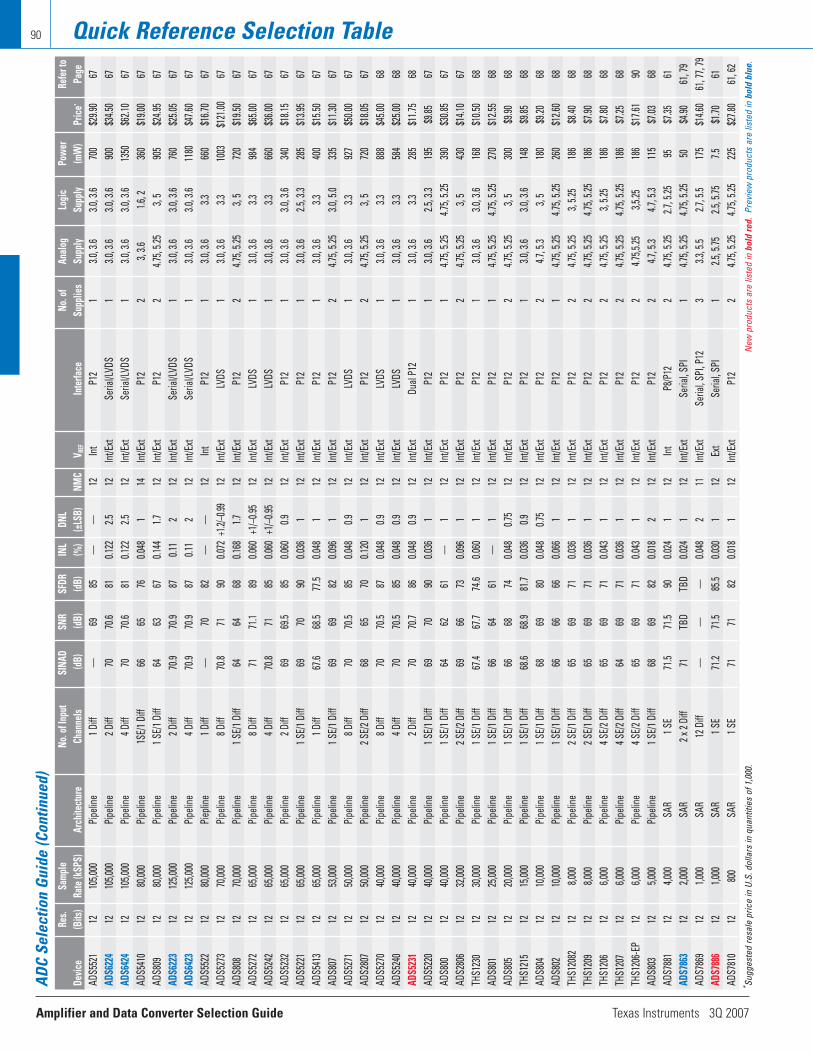
Amplifier and Data Converter Selection Guide Texas Instruments 3Q 2007
Quick Reference Selection Table90
Res.
Samp
leNo
. of I
nput
SINA
DSN
RSF
DRIN
LDN
LNo
. of
Anal
ogLo
gic
Pow
erRe
fer t
o De
vice
(Bits
)Ra
te (k
SPS)
Ar
chite
ctur
eCh
anne
ls(d
B)(d
B)(d
B)(%
)(±
LSB)
NMC
V REF
Inte
rface
Supp
lies
Supp
lySu
pply
(mW
)Pr
ice*
Page
AD
S552
112
105,0
00Pi
pelin
e1 D
iff—
6985
——
12In
tP1
21
3.0, 3
.63.0
, 3.6
700
$29.9
0 67
ADS6
224
1210
5,000
Pipe
line
2 Diff
7070
.681
0.122
2.512
Int/E
xtSe
rial/L
VDS
13.0
, 3.6
3.0, 3
.690
0$3
4.50
67AD
S642
412
105,0
00Pi
pelin
e4 D
iff70
70.6
810.1
222.5
12In
t/Ext
Seria
l/LVD
S1
3.0, 3
.63.0
, 3.6
1350
$62.1
067
ADS5
410
1280
,000
Pipe
line
1SE/
1 Diff
6665
760.0
481
14In
t/Ext
P12
23,
3.61.6
, 236
0$1
9.00
67AD
S809
1280
,000
Pipe
line
1 SE/
1 Diff
6463
670.1
441.7
12In
t/Ext
P12
24.7
5, 5.2
53,
590
5$2
4.95
67AD
S622
312
125,0
00Pi
pelin
e2 D
iff70
.970
.987
0.11
212
Int/E
xtSe
rial/L
VDS
13.0
, 3.6
3.0, 3
.676
0$2
5.05
67AD
S642
312
125,0
00Pi
pelin
e4 D
iff70
.970
.987
0.11
212
Int/E
xtSe
rial/L
VDS
13.0
, 3.6
3.0, 3
.611
80$4
7.60
67AD
S552
212
80,00
0Pi
eplin
e1 D
iff—
7082
——
12In
tP1
21
3.0, 3
.63.3
660
$16.7
0 67
ADS5
273
1270
,000
Pipe
line
8 Diff
70.8
7190
0.072
+1.2/
–0.99
12In
t/Ext
LVDS
13.0
, 3.6
3.310
03$1
21.00
67
ADS8
0812
70,00
0Pi
pelin
e1 S
E/1 D
iff64
6468
0.168
1.712
Int/E
xtP1
22
4.75,
5.25
3, 5
720
$19.5
0 67
ADS5
272
1265
,000
Pipe
line
8 Diff
7171
.189
0.060
+1/–
0.95
12In
t/Ext
LVDS
13.0
, 3.6
3.398
4$6
5.00
67AD
S524
212
65,00
0Pi
pelin
e4 D
iff70
.871
850.0
60+1
/–0.9
512
Int/E
xtLV
DS1
3.0, 3
.63.3
660
$36.0
0 67
ADS5
232
1265
,000
Pipe
line
2 Diff
6969
.585
0.060
0.912
Int/E
xtP1
21
3.0, 3
.63.0
, 3.6
340
$18.1
5 67
ADS5
221
1265
,000
Pipe
line
1 SE/
1 Diff
6970
900.0
361
12In
t/Ext
P12
13.0
, 3.6
2.5, 3
.328
5$1
3.95
67AD
S541
312
65,00
0Pi
pelin
e1 D
iff67
.668
.577
.50.0
481
12In
t/Ext
P12
13.0
, 3.6
3.340
0$1
5.50
67AD
S807
1253
,000
Pipe
line
1 SE/
1 Diff
6969
820.0
961
12In
t/Ext
P12
24.7
5, 5.2
53.0
, 5.0
335
$11.3
0 67
ADS5
271
1250
,000
Pipe
line
8 Diff
7070
.585
0.048
0.912
Int/E
xtLV
DS1
3.0, 3
.63.3
927
$50.0
0 67
ADS2
807
1250
,000
Pipe
line
2 SE/
2 Diff
6865
700.1
201
12In
t/Ext
P12
24.7
5, 5.2
53,
572
0$1
8.05
67AD
S527
012
40,00
0Pi
pelin
e8 D
iff70
70.5
870.0
480.9
12In
t/Ext
LVDS
13.0
, 3.6
3.388
8$4
5.00
68
ADS5
240
1240
,000
Pipe
line
4 Diff
7070
.585
0.048
0.912
Int/E
xtLV
DS1
3.0, 3
.63.3
584
$25.0
0 68
ADS5
231
1240
,000
Pipe
line
2 Diff
7070
.786
0.048
0.912
Int/E
xtDu
al P1
21
3.0, 3
.63.3
285
$11.7
5 68
ADS5
220
1240
,000
Pipe
line
1 SE/
1 Diff
6970
900.0
361
12In
t/Ext
P12
13.0
, 3.6
2.5, 3
.319
5$9
.85
67AD
S800
1240
,000
Pipe
line
1 SE/
1 Diff
6462
61—
112
Int/E
xtP1
21
4.75,
5.25
4.75,
5.25
390
$30.8
5 67
ADS2
806
1232
,000
Pipe
line
2 SE/
2 Diff
6966
730.0
961
12In
t/Ext
P12
24.7
5, 5.2
53,
543
0$1
4.10
67TH
S123
012
30,00
0Pi
pelin
e1 S
E/1 D
iff67
.467
.774
.60.0
601
12In
t/Ext
P12
13.0
, 3.6
3.0, 3
.616
8$1
0.50
68AD
S801
1225
,000
Pipe
line
1 SE/
1 Diff
6664
61—
112
Int/E
xtP1
21
4.75,
5.25
4.75,
5.25
270
$12.5
5 68
ADS8
0512
20,00
0Pi
pelin
e1 S
E/1 D
iff66
6874
0.048
0.75
12In
t/Ext
P12
24.7
5, 5.2
53,
530
0$9
.90
68TH
S121
512
15,00
0Pi
pelin
e1 S
E/1 D
iff68
.668
.981
.70.0
360.9
12In
t/Ext
P12
13.0
, 3.6
3.0, 3
.614
8$9
.85
68AD
S804
1210
,000
Pipe
line
1 SE/
1 Diff
6869
800.0
480.7
512
Int/E
xtP1
22
4.7, 5
.33,
518
0$9
.20
68AD
S802
1210
,000
Pipe
line
1 SE/
1 Diff
6666
660.0
661
12In
t/Ext
P12
14.7
5, 5.2
54.7
5, 5.2
526
0$1
2.60
68TH
S120
8212
8,000
Pipe
line
2 SE/
1 Diff
6569
710.0
361
12In
t/Ext
P12
24.7
5, 5.2
53,
5.25
186
$8.40
68
THS1
209
128,0
00Pi
pelin
e2 S
E/1 D
iff65
6971
0.036
112
Int/E
xtP1
22
4.75,
5.25
4.75,
5.25
186
$7.90
68
THS1
206
126,0
00Pi
pelin
e4 S
E/2 D
iff65
6971
0.043
112
Int/E
xtP1
22
4.75,
5.25
3, 5.2
518
6$7
.80
68TH
S120
712
6,000
Pipe
line
4 SE/
2 Diff
6469
710.0
361
12In
t/Ext
P12
24.7
5, 5.2
54.7
5, 5.2
518
6$7
.25
68TH
S120
6-EP
126,0
00Pi
pelin
e4 S
E/2 D
iff65
6971
0.043
112
Int/E
xtP1
22
4.75,5
.253,5
.2518
6$1
7.61
90AD
S803
125,0
00Pi
pelin
e1 S
E/1 D
iff68
6982
0.018
212
Int/E
xtP1
22
4.7, 5
.34.7
, 5.3
115
$7.03
68
ADS7
881
124,0
00SA
R1 S
E71
.571
.590
0.024
112
Int
P8/P
122
4.75,
5.25
2.7, 5
.2595
$7.35
61
ADS7
863
122,0
00SA
R2 x
2 Di
ff71
TBD
TBD
0.024
112
Int/E
xtSe
rial, S
PI1
4.75,
5.25
4.75,
5.25
50$4
.9061
, 79
ADS7
869
121,0
00SA
R12
Diff
——
—0.0
482
11In
t/Ext
Seria
l, SPI
, P12
33.3
, 5.5
2.7, 5
.517
5$1
4.60
61, 7
7, 79
ADS7
886
121,0
00SA
R1 S
E71
.271
.585
.50.0
301
12Ex
tSe
rial, S
PI1
2.5, 5
.752.5
, 5.75
7.5$1
.70
61AD
S781
012
800
SAR
1 SE
7171
820.0
181
12In
t/Ext
P12
24.7
5, 5.2
54.7
5, 5.2
522
5$2
7.80
61, 6
2
ADC
Sele
ctio
n Gu
ide
(Con
tinue
d)
* Sugg
este
d re
sale
pric
e in
U.S
. dol
lars
in q
uant
ities
of 1
,000
. N
ew p
rodu
cts
are
liste
d in
bol
d re
d. P
revi
ew p
rodu
cts
are
liste
d in
bol
d bl
ue.

Texas Instruments 3Q 2007 Amplifier and Data Converter Selection Guide
Quick Reference Selection Table 91
Res.
Samp
leNo
. of I
nput
SINA
DSN
RSF
DRIN
LDN
LNo
. of
Anal
ogLo
gic
Pow
erRe
fer t
o De
vice
(Bits
)Ra
te (k
SPS)
Ar
chite
ctur
eCh
anne
ls(d
B)(d
B)(d
B)(%
)(±
LSB)
NMC
V REF
Inte
rface
Supp
lies
Supp
lySu
pply
(mW
)Pr
ice*
Page
AD
S785
212
500
SAR
8 SE
7072
740.0
241
12In
t/Ext
P12
14.7
5, 5.2
54.7
5, 5.2
513
$3.40
61
ADS7
864
1250
0SA
R3 x
2 Di
ff71
7178
0.024
112
Int/E
xtP1
21
4.75,
5.25
4.75,
5.25
52.5
$6.65
61
, 79
ADS7
861
1250
0SA
R2 x
2 Di
ff70
7172
0.024
112
Int/E
xtSe
rial, S
PI1
4.75,
5.25
4.75,
5.25
25$4
.05
61, 7
9AD
S786
212
500
SAR
2 x 2
Diff
7171
780.0
241
12In
t/Ext
P12
14.7
5, 5.2
54.7
5, 5.2
525
$5.70
61
, 79
ADS7
818
1250
0SA
R1 P
Diff
7072
780.0
241
12In
tSe
rial, S
PI1
4.75,
5.25
4.75,
5.25
11$2
.50
61AD
S783
412
500
SAR
1 PDi
ff70
7278
0.024
112
Int
Seria
l, SPI
14.7
5, 5.2
54.7
5, 5.2
511
$2.45
61
ADS7
835
1250
0SA
R1 S
E72
7278
0.024
112
Int
Seria
l, SPI
14.7
5, 5.2
54.7
5, 5.2
517
.5$2
.75
61, 6
2TL
C255
812
400
SAR
8 SE
71—
840.0
241
12In
t/Ext
Seria
l, SPI
14.5
, 5.5
4.5, 5
.59.5
$5.30
62
TLC2
554
1240
0SA
R4 S
E71
—84
0.024
112
Int/E
xtSe
rial, S
PI1
4.5, 5
.54.5
, 5.5
9.5$5
.30
62TL
C255
212
400
SAR
2 SE
72—
840.0
241
12Ex
tSe
rial, S
PI1
4.5, 5
.54.5
, 5.5
15$3
.95
62TL
C255
112
400
SAR
1 SE
72—
840.0
241
12Ex
tSe
rial, S
PI1
4.5, 5
.54.5
, 5.5
15$3
.95
62TL
C255
512
400
SAR
1 Diff
72—
840.0
241
12In
tSe
rial, S
PI1
4.5, 5
.54.5
, 5.5
15$3
.95
91AD
S780
012
333
SAR
1 SE
7271
770.0
120.7
512
Int
P8/P
123
4.75,
5.25
4.75,
5.25
135
$30.5
0 62
ADS8
504
1225
0SA
R1 S
E72
7080
0.011
0.45
12In
t/Ext
P8/P
121
4.75,
5.25
4.75,
5.25
70$1
0.50
59, 6
2AD
S850
812
250
SAR
1 SE
7373
900.0
110.4
512
Int/E
xtSe
rial, S
PI1
4.75,
5.25
4.75,
5.25
70$1
0.50
59, 6
2AD
S784
412
200
SAR
8 SE/
4 Diff
7272
780.0
241
12Ex
tSe
rial, S
PI1
2.7, 5
.252.7
, 5.25
0.84
$2.90
62
TLC2
578
1220
0SA
R8 S
E79
8084
0.024
0.512
Ext
Seria
l, SPI
24.7
5, 5.5
2.7, 5
.529
$5.80
62
TLV2
548
1220
0SA
R8 S
E70
—84
0.024
112
Int/E
xtSe
rial, S
PI1
2.7, 5
.52.7
, 5.5
3.3$4
.85
63TL
V254
8M12
200
SAR
8 SE
71—
750.0
291
12In
t/Ext
Seria
l, SPI
12.7
, 5.5
2.7, 5
.53.3
$151
.89
91AD
S784
112
200
SAR
4 SE/
2 Diff
7272
790.0
241
12Ex
tSe
rial, S
PI1
2.7, 5
.252.7
, 5.25
0.84
$2.50
63
ADS7
842
1220
0SA
R4 S
E72
7279
0.024
112
Ext
P12
12.7
, 5.25
2.7, 5
.250.8
4$3
.10
63TL
C257
412
200
SAR
4 SE
7980
840.0
240.5
12Ex
tSe
rial, S
PI2
4.75,
5.52.7
, 5.5
29$5
.30
62TL
V254
412
200
SAR
4 SE
70—
840.0
241
12In
t/Ext
Seria
l, SPI
12.7
, 5.5
2.7, 5
.53.3
$4.20
63
TLV2
542
1220
0SA
R2 S
E72
—84
0.024
112
Ext
Seria
l, SPI
12.7
, 5.5
2.7, 5
.52.8
$3.85
63
AMC7
823
1220
0SA
R, D
AS1x
8 SE I
/O D
AS74
74—
0.024
112
Int/E
xtSe
rial, S
PI2
2.7, 5
.52.7
, 5.5
100
$9.75
62
, 77-
79TL
V255
312
200
SAR
11 S
E—
——
0.024
112
Ext
Seria
l, SPI
12.7
, 5.5
2.7, 5
.52.4
3$3
.40
63TL
V255
612
200
SAR
11 S
E—
——
0.024
112
Int/E
xtSe
rial, S
PI1
2.7, 5
.52.7
, 5.5
2.43
$3.55
63
ADS7
866
1220
0SA
R1 S
E70
71—
0.024
112
Ext
Seria
l, SPI
11.2
, 3.6
1.2, 3
.60.2
5$1
.8563
TLV2
541
1220
0SA
R1 S
E72
—84
0.024
112
Ext
Seria
l, SPI
12.7
, 5.5
2.7, 5
.52.8
$3.85
63
ADS7
816
1220
0SA
R1 P
Diff
7272
860.0
240.7
512
Ext
Seria
l, SPI
14.5
, 5.25
4.75,
5.25
1.9$1
.95
63AD
S781
712
200
SAR
1 Diff
7171
860.0
241
12Ex
tSe
rial, S
PI1
4.75,
5.25
4.75,
5.25
2.3$1
.95
63TL
V254
512
200
SAR
1 Diff
72—
840.0
241
12Ex
tSe
rial, S
PI1
2.7, 5
.52.7
, 5.5
2.8$3
.85
63AD
S782
212
200
SAR
1 Diff
71—
860.0
180.7
512
Ext
Seria
l, SPI
12.7
, 5.25
2.7, 5
.250.6
$1.55
63
ADS7
829
1212
5SA
R1 D
iff71
—86
0.018
0.75
12Ex
tSe
rial, S
PI1
2.7, 5
.252.7
. 5.25
0.6$1
.50
63AM
C782
012
100
SAR,
PGA
1x8 S
E I/O
72—
—0.0
241
12In
tSe
rial, S
PI2
4.75,
5.25
2.7, 5
.2540
$3.75
63
, 79
ADS7
804
1210
0SA
R1 S
E72
7080
0.011
0.45
12In
t/Ext
P8/P
121
4.75,
5.25
4.75,
5.25
81.5
$16.5
5 62
ADS8
506
1280
SAR
1SE
73—
—0.0
111
12In
t/Ext
Seria
l, SPI
14.7
5, 5.2
54.7
5, 5.2
524
$8.50
59, 6
2AD
S780
812
100
SAR
1 SE
7373
900.0
110.4
512
Int/E
xtSe
rial, S
PI1
4.75,
5.25
4.75,
5.25
81.5
$12.8
0 62
TLV2
543
1266
SAR
11 S
E—
——
0.024
112
Ext
Seria
l, SPI
14.5
, 5.5
4.5, 5
.53.3
$4.45
63AD
S782
812
50SA
R8 S
E/4 D
iff71
7286
0.024
112
Int/E
xtSe
rial, I
2 C1
2.7, 5
.252.7
, 5.25
0.675
$3.35
63
ADS7
870
1250
MUX
SAR
, PGA
8 SE
72—
—0.0
6—
12In
tSe
rial, S
PI1
2.7, 5
.252.7
, 5.25
4.6$4
.15
63, 7
9* Su
gges
ted
resa
le p
rice
in U
.S. d
olla
rs in
qua
ntiti
es o
f 1,0
00.
New
pro
duct
s ar
e lis
ted
in b
old
red.
Pre
view
pro
duct
s ar
e lis
ted
in b
old
blue
.
ADC
Sele
ctio
n Gu
ide
(Con
tinue
d)
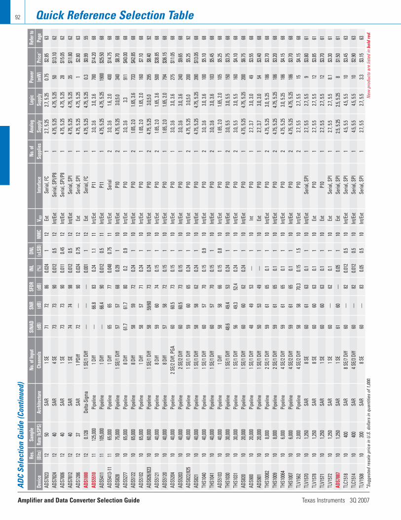
Amplifier and Data Converter Selection Guide Texas Instruments 3Q 2007
Quick Reference Selection Table92
Res.
Samp
leNo
. of I
nput
SINA
DSN
RSF
DRIN
LDN
LNo
. of
Anal
ogLo
gic
Pow
erRe
fer t
o De
vice
(Bits
)Ra
te (k
SPS)
Ar
chite
ctur
eCh
anne
ls(d
B)(d
B)(d
B)(%
)(±
LSB)
NMC
V REF
Inte
rface
Supp
lies
Supp
lySu
pply
(mW
)Pr
ice*
Page
AD
S782
312
50SA
R1 S
E71
7286
0.024
112
Ext
Seria
l, I2 C
12.7
, 5.25
2.7, 5
.250.7
5$2
.85
63AD
S782
412
40SA
R4 S
E73
7390
0.012
0.512
Int/E
xtSe
rial, S
PI/P
81
4.75,
5.25
4.75,
5.25
50$1
3.10
62AD
S780
612
40SA
R1 S
E73
7390
0.011
0.45
12In
t/Ext
Seria
l, SPI
/P8
14.7
5, 5.2
54.7
5, 5.2
528
$15.0
5 62
ADS7
812
1240
SAR
1 SE
7474
980.0
120.5
12In
t/Ext
Seria
l, SPI
14.7
5, 5.2
54.7
5, 5.2
535
$11.8
0 62
ADS1
286
1237
SAR
1 PDi
ff72
—90
0.024
0.75
12Ex
tSe
rial, S
PI1
4.75,
5.25
4.75,
5.25
1$2
.80
63AD
S100
012
0.128
Delta
-Sigm
a1 S
E/1 D
iff—
——
0.001
112
Ext
Seria
l, I2 C
14.7
5, 5.2
54.7
5, 5.2
50.3
$0.99
55
ADS5
510
1112
5,000
Pipe
line
1 Diff
—66
.883
0.24
1.111
Int/E
xtP1
11
3.0, 3
.63.0
, 3.6
780
$14.2
0 68
ADS5
411
1110
5,000
Pipe
line
1 Diff
—66
.490
0.012
0.511
Int/E
xtP1
11
4.75,
5.25
4.75,
5.25
1900
$25.5
0 68
ADS5
413-
1111
65,00
0Pi
pelin
e1 D
iff65
6577
0.048
0.75
11In
t/Ext
Seria
l2
3.0, 3
.61.6
, 2.0
400
$14.7
5 68
ADS8
2810
75,00
0Pi
pelin
e1 S
E/1 D
iff57
5768
0.29
110
Int/E
xtP1
02
4.75,
5.25
3.0,5.
034
0$8
.70
68AD
S527
710
65,00
0Pi
pelin
e8 D
iff61
.761
.780
0.20.9
10In
t/Ext
P10
13.0
, 3.6
3.391
1$4
0.00
68AD
S512
210
65,00
0Pi
pelin
e8 D
iff58
5972
0.24
110
Int/E
xtP1
02
1.65,
2.01.6
5, 3.6
733
$42.8
5 68
ADS5
102
1065
,000
Pipe
line
1 Diff
5857
710.2
41
10In
t/Ext
P10
11.6
5, 2.0
1.65,
2.016
0$7
.10
68AD
S826
/823
1060
,000
Pipe
line
1 SE/
1 Diff
5859
/6073
0.24
110
Int/E
xtP1
02
4.75,
5.25
3.0,5.
029
5$8
.40
92AD
S512
110
40,00
0Pi
pelin
e8 D
iff59
6074
0.15
110
Int/E
xtP1
02
1.65,
2.01.6
5, 3.6
500
$38.8
5 68
ADS5
120
1040
,000
Pipe
line
8 Diff
5758
720.1
51
10In
t/Ext
P10
11.6
5, 2.0
1.65,
2.079
4$3
6.15
68AD
S520
410
40,00
0Pi
pelin
e2 S
E/2 D
iff, P
GA60
60.5
730.1
51
10In
t/Ext
P10
13.0
, 3.6
3.0, 3
.627
5$1
1.05
68AD
S520
310
40,00
0Pi
pelin
e2 S
E/2 D
iff60
60.5
730.1
51
10In
t/Ext
P10
13.0
, 3.6
3.0, 3
.624
0$9
.65
68AD
S822
/825
1040
,000
Pipe
line
1 SE/
1 Diff
5960
650.2
41
10In
t/Ext
P10
24.7
5, 5.2
53.0
,5.0
200
$5.25
92
ADS8
2110
40,00
0Pi
pelin
e1 S
E/1 D
iff58
5862
0.24
110
Int/E
xtP1
01
4.75,
5.25
4.75,
5.25
390
$13.0
5 68
THS1
040
1040
,000
Pipe
line
1 SE/
1 Diff
6057
700.1
50.9
10In
t/Ext
P10
23.0
, 3.6
3.0, 3
.610
0$5
.10
68TH
S104
110
40,00
0Pi
pelin
e1 S
E/1 D
iff60
5770
0.15
110
Int/E
xtP1
02
3.0, 3
.63.0
, 3.6
103
$5.45
68
ADS5
103
1040
,000
Pipe
line
1 Diff
5858
660.1
50.8
10In
t/Ext
P10
11.6
5, 2.0
1.65,
2.010
5$5
.25
68TH
S103
010
30,00
0Pi
pelin
e1 S
E/1 D
iff48
.649
.453
0.24
110
Int/E
xtP1
02
3.0, 5
.53.0
, 5.5
150
$3.75
68
THS1
031
1030
,000
Pipe
line
1 SE/
1 Diff
5649
.352
.40.2
41
10In
t/Ext
P10
23.0
, 5.5
3.0, 5
.516
0$4
.10
68AD
S820
1020
,000
Pipe
line
1 SE/
1 Diff
6060
620.2
41
10In
t/Ext
P10
14.7
5, 5.2
54.7
5, 5.2
520
0$6
.75
68AD
S900
1020
,000
Pipe
line
1 SE/
1 Diff
4849
53—
110
Int
P10
12.7
, 3.7
3.0, 3
.049
$3.55
68
ADS9
0110
20,00
0Pi
pelin
e1 S
E/1 D
iff50
5349
—1
10Ex
tP1
01
2.7, 3
.73.0
, 3.0
54$3
.40
68TH
S100
8210
8,000
Pipe
line
2 SE/
1 Diff
5961
650.1
110
Int/E
xtP1
02
4.75,
5.25
3.0, 5
.2518
6$3
.7068
TH
S100
910
8,000
Pipe
line
2 SE/
1 Diff
5961
650.1
110
Int/E
xtP1
02
4.75,
5.25
4.75,
5.25
186
$3.20
68
THS1
0064
106,0
00Pi
pelin
e4 S
E/2 D
iff59
6165
0.11
10In
t/Ext
P10
24.7
5, 5.2
53.0
, 5.25
186
$4.15
68
THS1
007
106,0
00Pi
pelin
e4 S
E/2 D
iff59
6165
0.11
10In
t/Ext
P10
24.7
5, 5.2
54.7
5, 5.2
518
6$3
.70
68TL
V156
210
2,000
Pipe
line
4 SE/
2 Diff
5858
70.3
0.15
1.510
Int/E
xtP1
02
2.7, 5
.52.7
, 5.5
15$4
.15
68TL
V157
010
1,250
SAR
8 SE
6061
630.1
110
Int/E
xtSe
rial, S
PI1
2.7, 5
.52.7
, 5.5
9$3
.80
61TL
V157
810
1,250
SAR
8 SE
6060
630.1
110
Ext
P10
12.7
, 5.5
2.7, 5
.512
$3.85
61
TLV1
571
101,2
50SA
R1 S
E60
6063
0.11
10Ex
tP1
01
2.7, 5
.52.7
, 5.5
12$3
.70
61TL
V157
210
1,250
SAR
1 SE
60—
620.1
110
Ext
Seria
l, SPI
12.7
, 5.5
2.7, 5
.58.1
$3.30
61
ADS7
887
101,2
50SA
R1 S
E61
60—
0.05
110
Ext
Seria
l, SPI
12.5
, 5.25
2.5, 5
.258
$1.50
61
TLC1
518
1040
0SA
R8 S
E/7 D
iff60
—82
0.012
0.510
Int/E
xtSe
rial, S
PI1
4.5, 5
.54.5
, 5.5
10$3
.45
63TL
C151
410
400
SAR
4 SE/
3 Diff
60—
820.0
120.5
10In
t/Ext
Seria
l, SPI
14.5
, 5.5
4.5, 5
.510
$2.90
63
TLV1
508
1020
0SA
R8 S
E60
—83
0.05
0.510
Int/E
xtSe
rial, S
PI1
2.7, 5
.52.7
, 5.5
3.3$3
.15
63• Su
gges
ted
resa
le p
rice
in U
.S. d
olla
rs in
qua
ntiti
es o
f 1,0
00.
New
pro
duct
s ar
e lis
ted
in b
old
red.
ADC
Sele
ctio
n Gu
ide
(Con
tinue
d)
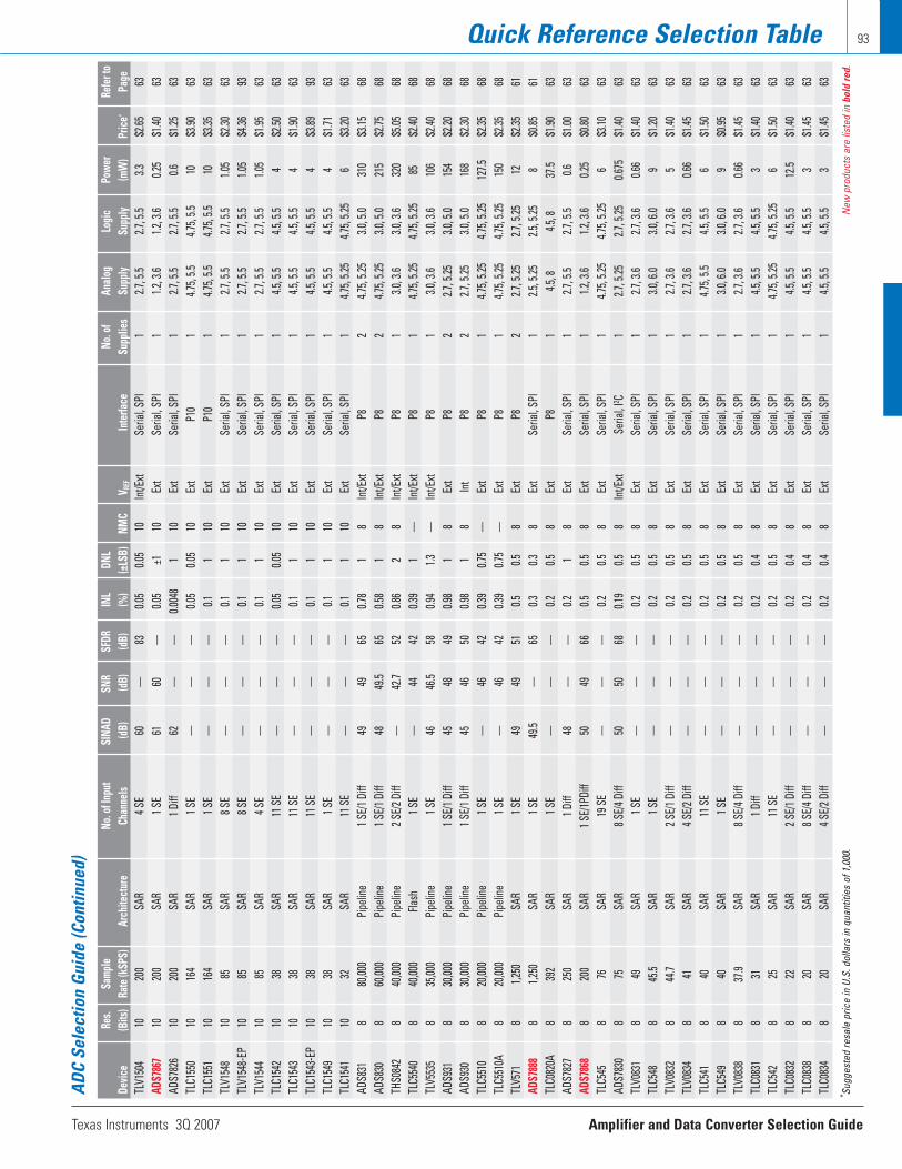
Texas Instruments 3Q 2007 Amplifier and Data Converter Selection Guide
Quick Reference Selection Table 93
Res.
Samp
leNo
. of I
nput
SINA
DSN
RSF
DRIN
LDN
LNo
. of
Anal
ogLo
gic
Pow
erRe
fer t
o De
vice
(Bits
)Ra
te (k
SPS)
Ar
chite
ctur
eCh
anne
ls(d
B)(d
B)(d
B)(%
)(±
LSB)
NMC
V REF
Inte
rface
Supp
lies
Supp
lySu
pply
(mW
)Pr
ice*
Page
TL
V150
410
200
SAR
4 SE
60—
830.0
50.0
510
Int/E
xtSe
rial, S
PI1
2.7, 5
.52.7
, 5.5
3.3$2
.65
63AD
S786
710
200
SAR
1 SE
6160
—0.0
5±1
10Ex
tSe
rial, S
PI1
1.2, 3
.61.2
, 3.6
0.25
$1.40
63
ADS7
826
1020
0SA
R1 D
iff62
——
0.004
81
10Ex
tSe
rial, S
PI1
2.7, 5
.52.7
, 5.5
0.6$1
.25
63TL
C155
010
164
SAR
1 SE
——
—0.0
50.0
510
Ext
P10
14.7
5, 5.5
4.75,
5.510
$3.90
63
TLC1
551
1016
4SA
R1 S
E—
——
0.11
10Ex
tP1
01
4.75,
5.54.7
5, 5.5
10$3
.35
63TL
V154
810
85SA
R8 S
E—
——
0.11
10Ex
tSe
rial, S
PI1
2.7, 5
.52.7
, 5.5
1.05
$2.30
63
TLV1
548-
EP10
85SA
R8 S
E—
——
0.11
10Ex
tSe
rial, S
PI1
2.7, 5
.52.7
, 5.5
1.05
$4.36
93
TLV1
544
1085
SAR
4 SE
——
—0.1
110
Ext
Seria
l, SPI
12.7
, 5.5
2.7, 5
.51.0
5$1
.95
63TL
C154
210
38SA
R11
SE
——
—0.0
50.0
510
Ext
Seria
l, SPI
14.5
, 5.5
4.5, 5
.54
$2.50
63
TLC1
543
1038
SAR
11 S
E—
——
0.11
10Ex
tSe
rial, S
PI1
4.5, 5
.54.5
, 5.5
4$1
.90
63TL
C154
3-EP
1038
SAR
11 S
E—
——
0.11
10Ex
tSe
rial, S
PI1
4.5, 5
.54.5
, 5.5
4$3
.89
93TL
C154
910
38SA
R1 S
E—
——
0.11
10Ex
tSe
rial, S
PI1
4.5, 5
.54.5
, 5.5
4$1
.71
63TL
C154
110
32SA
R11
SE
——
—0.1
110
Ext
Seria
l, SPI
14.7
5, 5.2
54.7
5, 5.2
56
$3.20
63
ADS8
318
80,00
0Pi
pelin
e1 S
E/1 D
iff49
4965
0.78
18
Int/E
xtP8
24.7
5, 5.2
53.0
, 5.0
310
$3.15
68
ADS8
308
60,00
0Pi
pelin
e1 S
E/1 D
iff48
49.5
650.5
81
8In
t/Ext
P82
4.75,
5.25
3.0, 5
.021
5$2
.75
68TH
S084
28
40,00
0Pi
pelin
e2 S
E/2 D
iff—
42.7
520.8
62
8In
t/Ext
P81
3.0, 3
.63.0
, 3.6
320
$5.05
68
TLC5
540
840
,000
Flash
1 SE
—44
420.3
91
—In
t/Ext
P81
4.75,
5.25
4.75,
5.25
85$2
.40
68TL
V553
58
35,00
0Pi
pelin
e1 S
E46
46.5
580.9
41.3
—In
t/Ext
P81
3.0, 3
.63.0
, 3.6
106
$2.40
68
ADS9
318
30,00
0Pi
pelin
e1 S
E/1 D
iff45
4849
0.98
18
Ext
P82
2.7, 5
.253.0
, 5.0
154
$2.20
68
ADS9
308
30,00
0Pi
pelin
e1 S
E/1 D
iff45
4650
0.98
18
Int
P82
2.7, 5
.253.0
, 5.0
168
$2.30
68
TLC5
510
820
,000
Pipe
line
1 SE
—46
420.3
90.7
5—
Ext
P81
4.75,
5.25
4.75,
5.25
127.5
$2.35
68
TLC5
510A
820
,000
Pipe
line
1 SE
—46
420.3
90.7
5—
Ext
P81
4.75,
5.25
4.75,
5.25
150
$2.35
68
TLV5
718
1,250
SAR
1 SE
4949
510.5
0.58
Ext
P82
2.7, 5
.252.7
, 5.25
12$2
.35
61AD
S788
88
1,250
SAR
1 SE
49.5
—65
0.30.3
8Ex
tSe
rial, S
PI1
2.5, 5
.252.5
, 5.25
8$0
.85
61TL
C082
0A8
392
SAR
1 SE
——
—0.2
0.58
Ext
P81
4.5, 8
4.5, 8
37.5
$1.90
63
ADS7
827
825
0SA
R1 D
iff48
——
0.21
8Ex
tSe
rial, S
PI1
2.7, 5
.52.7
, 5.5
0.6$1
.00
63AD
S786
88
200
SAR
1 SE/
1PDi
ff50
4966
0.50.5
8Ex
tSe
rial, S
PI1
1.2, 3
.61.2
, 3.6
0.25
$0.80
63
TLC5
458
76SA
R19
SE
——
—0.2
0.58
Ext
Seria
l, SPI
14.7
5, 5.2
54.7
5, 5.2
56
$3.10
63
ADS7
830
875
SAR
8 SE/
4 Diff
5050
680.1
90.5
8In
t/Ext
Seria
l, I2 C
12.7
, 5.25
2.7, 5
.250.6
75$1
.40
63TL
V083
18
49SA
R1 S
E—
——
0.20.5
8Ex
tSe
rial, S
PI1
2.7, 3
.62.7
, 3.6
0.66
$1.40
63
TLC5
488
45.5
SAR
1 SE
——
—0.2
0.58
Ext
Seria
l, SPI
13.0
, 6.0
3.0, 6
.09
$1.20
63
TLV0
832
844
.7SA
R2 S
E/1 D
iff—
——
0.20.5
8Ex
tSe
rial, S
PI1
2.7, 3
.62.7
, 3.6
5$1
.40
63TL
V083
48
41SA
R4 S
E/2 D
iff—
——
0.20.5
8Ex
tSe
rial, S
PI1
2.7, 3
.62.7
, 3.6
0.66
$1.45
63
TLC5
418
40SA
R11
SE
——
—0.2
0.58
Ext
Seria
l, SPI
14.7
5, 5.5
4.5, 5
.56
$1.50
63
TLC5
498
40SA
R1 S
E—
——
0.20.5
8Ex
tSe
rial, S
PI1
3.0, 6
.03.0
, 6.0
9$0
.95
63TL
V083
88
37.9
SAR
8 SE/
4 Diff
——
—0.2
0.58
Ext
Seria
l, SPI
12.7
, 3.6
2.7, 3
.60.6
6$1
.45
63TL
C083
18
31SA
R1 D
iff—
——
0.20.4
8Ex
tSe
rial, S
PI1
4.5, 5
.54.5
, 5.5
3$1
.40
63TL
C542
825
SAR
11 S
E—
——
0.20.5
8Ex
tSe
rial, S
PI1
4.75,
5.25
4.75,
5.25
6$1
.50
63TL
C083
28
22SA
R2 S
E/1 D
iff—
——
0.20.4
8Ex
tSe
rial, S
PI1
4.5, 5
.54.5
, 5.5
12.5
$1.40
63
TLC0
838
820
SAR
8 SE/
4 Diff
——
—0.2
0.48
Ext
Seria
l, SPI
14.5
, 5.5
4.5, 5
.53
$1.45
63
TLC0
834
820
SAR
4 SE/
2 Diff
——
—0.2
0.48
Ext
Seria
l, SPI
14.5
, 5.5
4.5, 5
.53
$1.45
63
* Sugg
este
d re
sale
pric
e in
U.S
. dol
lars
in q
uant
ities
of 1
,000
. N
ew p
rodu
cts
are
liste
d in
bol
d re
d.
ADC
Sele
ctio
n Gu
ide
(Con
tinue
d)
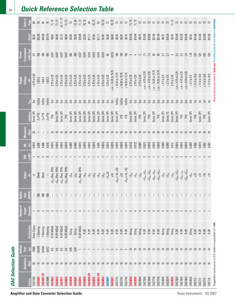
Amplifier and Data Converter Selection Guide Texas Instruments 3Q 2007
Quick Reference Selection Table94
Settl
ing
Numb
er of
Upda
teSu
pply
Pow
erRe
solu
tion
Time
Outp
utRa
teOu
tput
DNL
INL
Mon
oton
icVo
ltage
Cons
umpt
ion
Refe
r to
Devic
e(B
its)
(µs)
Arch
itect
ure
Chan
nels
(MSP
S)(V
)(±
LSB)
(%)
(Bits
)In
terfa
ceV R
EF(V
)(m
W) (
Typ)
Pric
e*Pa
geDA
C122
020
1500
0De
lta-S
igma
1—
+51
0.001
520
Seria
l, SPI
Ext
+ 4.75
to 5.
252.5
$6.33
69
DAC5
687
160.0
104
I-Ste
ering
250
020
mA4
0.006
—2 x
P16
Int/E
xt1.8
/3.3
700
$22.5
0 76
DAC5
687-
EP16
0.010
4I-S
teer
ing2
500
20mA
50.0
06—
2 x P
16In
t/Ext
1.8/3.
370
0$4
3.99
94DA
C568
616
0.012
I-Ste
ering
250
0—
90.0
18—
2 x P
16In
t/Ext
1.8/3.
340
0$1
9.75
76DA
C882
216
0.5R-
2R M
DAC
2—
±VRE
F(R
eq. O
PA)
10.0
015
16P1
6Ex
t2.7
5 to 5
.250.0
27$8
.6571
, 72
DAC8
812
160.5
R-2R
MDA
C2
—±V
REF
(Req
. OPA
)1
0.001
516
Seria
l, SPI
Ext
2.75 t
o 5.25
0.027
$8.40
71
, 72
DAC8
811
160.5
R-2R
MDA
C1
—±V
REF
(Req
. OPA
)1
0.001
516
Seria
l, SPI
Ext
2.75 t
o 5.25
0.027
$7.15
42
, 71,
72DA
C882
016
0.5R-
2R M
DAC
1—
±VRE
F(R
eq. O
PA)
10.0
015
16P1
6Ex
t2.7
5 to 5
.250.0
27$8
.50
71, 7
2DA
C858
016
0.65
Strin
g1
—±V
REF
10.0
987
16Se
rial, S
PIEx
t2.7
5 to 5
.2520
0$3
.00
72DA
C858
116
0.65
Strin
g1
—±V
REF
10.0
987
16Se
rial, S
PIEx
t2.7
5 to 5
.2520
0$3
.00
72, 9
4DA
C881
416
1R-
2R M
DAC
4—
±VRE
F(R
eq. O
PA)
10.0
015
16Se
rial, S
PIEx
t2.7
5 to 5
.250.0
27$1
6.95
71, 7
2DA
C883
016
1R-
2R1
—+V
REF
10.0
015
16Se
rial, S
PIEx
t2.7
5 to 5
.250.0
15$7
.95
70, 7
2DA
C883
0-EP
161
R-2R
1—
+VRE
F1
0.001
516
Seria
l, SPI
Ext
2.75 t
o 5.25
0.015
$17.1
1 94
DAC8
831
161
R-2R
1—
±VRE
F1
0.001
516
Seria
l, SPI
Ext
2.75 t
o 5.25
0.015
$7.95
70
, 72
DAC8
831-
EP16
1R-
2R1
—±V
REF
10.0
0416
Seria
l, SPI
Ext
2.75 t
o 5.25
0.015
$17.1
1 94
DAC8
832
161
R-2R
1—
±VRE
F1
0.001
516
Seria
l, SPI
Ext
2.75 t
o 5.25
0.015
$7.95
70
, 72
DAC8
881
162
R-2R
1—
+VRE
F(5)
10.0
015
16Se
rial, S
PIEx
t2.7
5 to 5
.2560
$8.00
72DA
C887
116
5R-
2R1
—±1
01
0.001
516
Seria
l, SPI
Ext
±or +
14.25
to 15
.750.0
15$8
.0070
, 72
DAC7
731
165
R-2R
1—
+VRE
F (+10
, ±10
)1
0.001
516
Seria
l, SPI
Int/E
xt±1
4.25 t
o 15.7
510
0$8
.20
72DA
C774
116
5R-
2R1
—±1
0 1
0.001
516
P16
Int/E
xt±1
4.25 t
o 15.7
510
0$8
.30
72DA
C774
216
5R-
2R1
—+V
REF (+
10, ±
10)
10.0
015
16P1
6In
t/Ext
±14.2
5 to 1
5.75
100
$8.70
72
DAC8
554
1610
Strin
g4
—+V
REF
10.0
122
16Se
rial, S
PIEx
t2.7
5 to 5
.254
$10.4
0 71
, 73
DAC8
555
1610
Strin
g4
—+V
REF
10.0
122
16Se
rial, S
PIEx
t2.7
5 to 5
.254
$10.4
0 71
, 73
DAC8
544
1610
Strin
g4
—+V
REF
10.0
987
16P1
6Ex
t2.7
5 to 5
.252
$9.75
73
DAC7
634
1610
R-2R
4—
+VRE
F, ±V R
EF2
0.001
515
Seria
l, SPI
Ext
±or +
4.75
to 5.
257.5
$19.9
5 72
DAC7
644
1610
R-2R
4—
+VRE
F, ±V R
EF2
0.001
515
P16
Ext
±or +
4.75
to 5.
257.5
$19.9
5 72
DAC7
734
1610
R-2R
4—
+VRE
F, ±V R
EF1
0.001
516
Seria
l, SPI
Ext
±or +
14.25
to 15
.7550
$31.4
5 72
DAC7
744
1610
R-2R
4—
+VRE
F, ±V R
EF1
0.001
516
P16
Ext
±or +
14.25
to 15
.7550
$31.4
5 72
DAC8
534
1610
Strin
g4
—+V
REF
10.0
987
16Se
rial, S
PIEx
t+ 2
.7 to
5.5
2.7$8
.75
73DA
C857
416
10St
ring
4—
+VRE
F1
0.098
716
Seria
l, I2 C
Ext
+ 2.7
to 5.
52.7
$10.2
5 73
DAC8
552
1610
Strin
g2
—+V
REF
10.0
1216
Seria
l, SPI
Ext
2.75 t
o 5.25
2$5
.45
71, 7
3DA
C763
216
10R-
2R2
—+V
REF, ±
V REF
20.0
015
15Se
rial, S
PIEx
t±o
r + 4.
75 to
5.25
2.5$1
0.45
72DA
C764
216
10R-
2R2
—+V
REF, ±
REF
20.0
015
15P1
6Ex
t±o
r + 4.
75 to
5.25
2.5$1
0.55
72DA
C764
316
10R-
2R2
—+V
REF, ±
V REF
20.0
015
15P1
6Ex
t±o
r + 4.
75 to
5.25
2.5$1
0.55
72DA
C853
216
10St
ring
2—
+VRE
F1
0.098
716
Seria
l, SPI
Ext
+ 2.7
to 5.
51.3
5$5
.35
73DA
C712
1610
R-2R
1—
±10
10.0
0315
P16
Int
±11.4
to 16
.552
5$1
4.50
72DA
C714
1610
R-2R
1—
±10
10.0
015
16Se
rial, S
PIIn
t±1
1.4 to
16.5
525
$14.5
0 72
DAC7
1516
10R-
2R1
—+1
01
0.003
16P1
6In
t±1
1.4 to
16.5
525
$15.8
5 73
DAC7
1616
10R-
2R1
—+1
02
0.003
16Se
rial, S
PIIn
t±1
1.4 to
16.5
525
$15.8
5 73
DAC
Sele
ctio
n Gu
ide
* Sugg
este
d re
sale
pric
e in
U.S
. dol
lars
in q
uant
ities
of 1
,000
. N
ew p
rodu
cts
are
liste
d in
bol
d re
d. P
revi
ew p
rodu
cts
are
liste
d in
bol
d bl
ue.

Texas Instruments 3Q 2007 Amplifier and Data Converter Selection Guide
Quick Reference Selection Table 95
DAC
Sele
ctio
n Gu
ide
(Con
tinue
d)Nu
mber
ofUp
date
Supp
lyPo
wer
Settl
ing
Numb
er of
Upda
teSu
pply
Pow
erRe
solu
tion
Time
Outp
utRa
teOu
tput
DNL
INL
Mon
oton
icVo
ltage
Cons
umpt
ion
Refe
r to
Devic
e(B
its)
(µs)
Arch
itect
ure
Chan
nels
(MSP
S)(V
)(±
LSB)
(%)
(Bits
)In
terfa
ceV R
EF(V
)(m
W) (
Typ)
Pric
e*Pa
geDA
C763
116
10R-
2R1
—+V
REF, ±
V REF
20.0
015
15Se
rial, S
PIEx
t±o
r + 4.
75 to
5.25
1.8$5
.85
72DA
C764
116
10R-
2R1
—+V
REF, ±
V REF
20.0
015
15P1
6Ex
t±o
r + 4.
75 to
5.25
1.8$6
.30
72DA
C855
116
10St
ring
1—
+VRE
F1
0.012
16Se
rial, S
PIEx
t2.7
5 to 5
.251
$2.65
71, 7
3DA
C855
016
10St
ring
1—
+VRE
F1
0.012
16Se
rial, S
PIEx
t2.7
5 to 5
.251
$2.65
71
, 73
DAC8
564
1610
Strin
g4
—+V
REF (+
2.5)
10.0
1216
Seria
l, SPI
Int/E
xt2.7
5 to 5
.255
$10.4
573
DAC8
565
1610
Strin
g4
—+V
REF (+
2.5)
10.0
1216
Seria
l, SPI
Int/E
xt2.7
5 to 5
.255
$10.4
573
DAC8
560
1610
Strin
g1
—+V
REF (+
2.5)
10.0
1216
Seria
l, SPI
Int/E
xt2.7
5 to 5
.252.6
$3.50
71
, 73
DAC8
501
1610
Strin
g MDA
C1
—+V
REF/M
DAC
10.0
987
16Se
rial, S
PIEx
t+ 2
.7 to
5.5
0.72
$3.00
73
DAC8
531
1610
Strin
g1
—+V
REF
10.0
987
16Se
rial, S
PIEx
t+ 2
.7 to
5.5
0.72
$3.00
75
DAC8
541
1610
Strin
g1
—+V
REF
10.0
9616
P16
Ext
+ 2.7
to 5.
50.7
2$3
.00
73DA
C857
116
10St
ring
1—
+VRE
F1
0.098
716
Seria
l, I2 C
Ext
+ 2.7
to 5.
50.4
2$2
.95
73DA
C765
416
12R-
2R4
—±2
.51
0.001
516
Seria
l, SPI
Int
±or +
4.75
to 5.
2518
$21.8
0 72
DAC7
664
1612
R-2R
4—
±2.5
10.0
015
16P1
6In
t±o
r + 4.
75 to
5.25
18$2
0.75
72DA
C122
116
2000
Delta
-Sigm
a1
—2.5
10.0
015
16Se
rial, S
PIEx
t+ 2
.7 to
3.3
1.2$5
.01
69DA
C567
514
0.005
I-Ste
ering
140
020
mA2
0.006
—LV
DS/P
14In
t/Ext
382
0$2
9.45
76DA
C567
5-EP
140.0
05I-S
teer
ing1
400
20mA
20.0
24—
LVDS
/P14
Int/E
xt+ 3
.15 to
3.6
820
$50.0
0 95
DAC5
672
140.0
2I-S
teer
ing2
200
20mA
30.0
24—
2 x P
14In
t3.0
to 5.
2533
0$1
3.25
76DA
C567
2-EP
140.0
2I-S
teer
ing2
200
20mA
30.0
24—
2 x P
14In
t3.0
to 5.
2533
0$2
5.91
95DA
C290
414
0.03
I-Ste
ering
212
520
mA4
0.03
—2 x
P14
Int/E
xt+ 3
.0 to
5.5
310
$13.2
5 76
DAC9
0414
0.03
I-Ste
ering
116
520
mA1.7
50.0
15—
P14
Int/E
xt+ 3
.0 to
5.5
170
$6.25
76
DAC8
803
140.5
R-2R
MDA
C4
—±V
REF
(Req
. OPA
)1
0.006
114
Seria
l, SPI
Ext
2.75 t
o 5.25
0.027
$12.6
5 71
, 72
DAC8
802
140.5
R-2R
MDA
C2
—±V
REF
(Req
. OPA
)1
0.006
114
Seria
l, SPI
Ext
2.75 t
o 5.25
0.027
$6.10
71
, 72
DAC8
805
140.5
R-2R
MDA
C2
—±V
REF
(Req
. OPA
)1
0.006
116
P14
Ext
2.75 t
o 5.25
0.027
$6.15
71
, 72
DAC8
801
140.5
R-2R
MDA
C1
—±V
REF
(Req
. OPA
)1
0.006
114
Seria
l, SPI
Ext
2.75 t
o 5.25
0.027
$4.60
71
, 72
DAC8
806
140.5
R-2R
MDA
C1
—±V
REF
(Req
. OPA
)1
0.006
116
P14
Ext
2.75 t
o 5.25
0.027
$5.50
71
, 72
DAC5
662
120.0
2I-S
teer
ing2
200
20mA
20.0
488
—Se
rial
Ext
+3.0
to 3.
633
0$1
0.70
76DA
C566
2-EP
120.0
2I-S
teer
ing2
200
20mA
20.0
488
—Se
rial
Ext
+3.0
to 3.
633
0$2
0.92
95DA
C567
412
0.02
I-Ste
ering
140
020
mA2
0.085
—P1
4In
t/Ext
1.8/3.
342
0$1
5.00
74DA
C293
212
0.025
I-Ste
ering
240
2mA
0.50.0
488
—P1
2In
t/Ext
+2.7
to 3.
329
$8.35
76
DAC2
902
120.0
3I-S
teer
ing2
125
20mA
2.50.0
732
—2 x
P12
Int/E
xt+3
.0 to
5.25
310
$15.4
1 76
DAC9
0212
0.03
I-Ste
ering
116
520
mA1.7
50.0
61—
P12
Int/E
xt+3
.0 to
5.25
170
$6.25
76
THS5
661A
120.0
35I-S
teer
ing1
125
20mA
20.0
976
—P1
2In
t/Ext
+3.0
to 5.
2517
5$6
.25
76DA
C782
212
0.5R-
2R M
DAC
2—
±VRE
F(R
eq. O
PA)
10.0
244
12P1
2Ex
t2.7
5 to 5
.250.0
27$3
.80
71, 7
2DA
C781
112
0.5R-
2R M
DAC
1—
±VRE
F(R
eq. O
PA)
10.0
244
12Se
rial, S
PIEx
t2.7
5 to 5
.250.0
25$2
.55
42, 7
1, 72
DAC7
821
120.5
R-2R
MDA
C1
—±V
REF
(Req
. OPA
)1
0.024
412
P12
Ext
2.75 t
o 5.25
0.027
$2.60
71
, 72
DAC7
800
120.8
R-2R
2—
1mA
10.0
1212
Seria
l, SPI
Ext
+ 4.5
to 5.
51
$13.5
5 72
DAC7
801
120.8
R-2R
2—
1mA
10.0
1212
P(8+
4)Ex
t+ 4
.5 to
5.5
1$1
7.95
72DA
C780
212
0.8R-
2R2
—1m
A1
0.012
12P1
2Ex
t+ 4
.5 to
5.5
1$1
4.00
72TL
V561
012
1St
ring
8—
+VRE
F1
0.412
Seria
l, SPI
Ext
+ 2.7
to 5.
518
$8.50
73
* Sugg
este
d re
sale
pric
e in
U.S
. dol
lars
in q
uant
ities
of 1
,000
. N
ew p
rodu
cts
are
liste
d in
bol
d re
d. P
revi
ew p
rodu
cts
are
liste
d in
bol
d bl
ue.

Amplifier and Data Converter Selection Guide Texas Instruments 3Q 2007
Quick Reference Selection Table96DA
C Se
lect
ion
Guid
e (C
ontin
ued)
Numb
er of
Upda
teSu
pply
Pow
er
Settl
ing
Numb
er of
Upda
teSu
pply
Pow
erRe
solu
tion
Time
Outp
utRa
teOu
tput
DNL
INL
Mon
oton
icVo
ltage
Cons
umpt
ion
Refe
r to
Devic
e(B
its)
(µs)
Arch
itect
ure
Chan
nels
(MSP
S)(V
)(±
LSB)
(%)
(Bits
)In
terfa
ceV R
EF(V
)(m
W) (
Typ)
Pric
e*Pa
geTL
V563
012
1St
ring
8—
+VRE
F1
0.412
Seria
l, SPI
Int/E
xt+ 2
.7 to
5.5
18$8
.85
73TL
V563
812
1St
ring
2—
+VRE
F (+2,
4) 1
0.112
Seria
l, SPI
Int/E
xt+ 2
.7 to
5.25
4.5$3
.25
73TL
V563
8-EP
121
Strin
g2
—+V
REF (+
2, 4)
10.1
12Se
rial, S
PIIn
t/Ext
+ 2.7
to 5.
254.5
$9.34
96
TLV5
638M
121
Strin
g2
—+V
REF (+
2, 4)
10.1
12Se
rial, S
PIIn
t/Ext
+ 2.7
to 5.
254.5
$32.5
0 96
DAC7
541
121
R-2R
MDA
C1
—±V
REF
(Req
. OPA
)0.5
0.012
12P1
2Ex
t+ 5
to 16
30$6
.70
72DA
C804
312
1R-
2R M
DAC
1—
±VRE
F(R
eq. O
PA)
10.0
1212
Seria
l, SPI
Ext
+ 4.75
to 5.
252.5
$3.60
73
TLV5
613
121
Strin
g1
—+V
REF
10.1
12P8
Ext
+ 2.7
to 5.
51.2
$2.60
73
TLV5
619
121
Strin
g1
—+V
REF
10.0
812
P12
Ext
+ 2.7
to 5.
54.3
$2.60
73
TLV5
633
121
Strin
g1
—+V
REF (+
2, 4)
0.50.0
812
P8In
t/Ext
+ 2.7
to 5.
52.7
$4.70
73
TLV5
636
121
Strin
g1
—+V
REF (+
2, 4)
10.1
12Se
rial, S
PIIn
t/Ext
+ 2.7
to 5.
254.5
$3.65
73
TLV5
639
121
Strin
g1
—+V
REF (+
2, 4)
0.50.1
12P1
2In
t/Ext
+ 2.7
to 5.
252.7
$3.45
73
TLV5
619-
EP12
1St
ring
1—
+VRE
F1
0.08
12P1
2Ex
t+ 2
.7 to
5.5
4.3$7
.91
96DA
C754
512
2R-
2R M
DAC
1—
±VRE
F (Req
. OPA
)1
0.012
12P1
2Ex
t+ 5
to 16
30$5
.25
73TL
V561
8A12
2.5St
ring
2—
+VRE
F1
0.08
12Se
rial, S
PIEx
t+ 2
.7 to
5.5
1.8$4
.75
73TL
V561
8A-E
P12
2.5St
ring
2—
+VRE
F1
0.08
12Se
rial, S
PIEx
t+2
.7 to
5.5
1.8$1
1.78
96TL
V561
412
3St
ring
4—
+VRE
F1
0.112
Seria
l, SPI
Ext
+ 2.7
to 5.
53.6
$7.45
74
TLV5
618A
M12
3St
ring
2—
+VRE
F1
0.112
Seria
l, SPI
Ext
+2.7
to 5.
51.8
$28.2
3 96
TLV5
616
123
Strin
g1
—+V
REF
10.1
12Se
rial, S
PIEx
t+ 2
.7 to
5.5
0.9$2
.60
73DA
C811
124
R-2R
1—
+10,
±5, 1
0 0.5
0.006
12P1
2In
t±o
r + 11
.4 to
16.5
625
$11.0
0 73
DAC8
1312
4R-
2R1
—+V
REF (+
10, ±
5, 10
) 0.5
0.006
12P1
2In
t/Ext
±or +
11.4
to 16
.527
0$1
2.60
73DA
C755
812
5St
ring
8—
+VRE
F1
0.012
12Se
rial, S
PIEx
t2.7
5 to 5
.252.7
$7.50
74
DAC7
554
125
Strin
g4
—+V
REF
10.0
1212
Seria
l, SPI
Ext
2.75 t
o 5.25
1.5$4
.80
74DA
C755
212
5St
ring
2—
+VRE
F1
0.024
12Se
rial, S
PIEx
t2.7
5 to 5
.250.6
75$2
.35
74DA
C755
312
5St
ring
2—
+VRE
F1
0.024
12Se
rial, S
PIEx
t2.7
5 to 5
.250.6
75$2
.35
74DA
C755
112
5St
ring
1—
+VRE
F1
0.024
12Se
rial, S
PIEx
t2.7
5 to 5
.250.2
7$1
.40
74DA
C757
312
10St
ring
4—
+VRE
F1
0.096
12Se
rial, I
2 CEx
t2.7
5 to 5
.251.8
$6.15
74
DAC7
574
1210
Strin
g4
—+V
REF
—0.0
9612
Seria
l, I2 C
Ext
+ 2.7
to 5.
51.8
$6.15
74
DAC7
614
1210
R-2R
4—
+VRE
F, ±V R
EF1
0.012
12Se
rial, S
PIEx
t±o
r + 4.
75 to
5.25
15$6
.70
73DA
C761
512
10R-
2R4
—+V
REF, ±
V REF
10.0
1212
Seria
l, SPI
Ext
±or +
4.75
to 5.
2515
$6.70
73
DAC7
616
1210
R-2R
4—
+VRE
F, ±V R
EF1
0.012
12Se
rial, S
PIEx
t+ 3
to 3.
62.4
$5.40
73
DAC7
617
1210
R-2R
4—
+VRE
F, ±V R
EF1
0.012
12Se
rial, S
PIEx
t+ 3
to 3.
62.4
$5.40
73
DAC7
624
1210
R-2R
4—
±VRE
F1
0.012
12P1
2Ex
t±o
r + 4.
75 to
5.25
15$1
0.25
73DA
C762
512
10R-
2R4
—±V
REF
10.0
1212
P12
Ext
±or +
4.75
to 5.
2515
$10.2
5 73
DAC7
714
1210
R-2R
4—
±VRE
F1
0.012
12Se
rial, S
PIEx
t±o
r + 14
.25 to
15.75
45$1
1.45
73DA
C771
512
10R-
2R4
—±V
REF
10.0
1212
Seria
l, SPI
Ext
±or +
14.25
to 15
.7545
$11.4
5 73
DAC7
724
1210
R-2R
4—
±VRE
F1
0.012
12P1
2Ex
t±o
r + 14
.25 to
15.75
45$1
1.85
73DA
C772
512
10R-
2R4
—±V
REF
10.0
1212
P12
Ext
±or +
14.25
to 15
.7545
$11.8
5 73
DAC7
612
1210
R-2R
2—
+4.09
61
0.012
12Se
rial, S
PIIn
t+ 4
.75 to
5.25
3.5$3
.10
74DA
C751
212
10St
ring
1—
+VDD
10.3
812
Seria
l, SPI
Ext
+ 2.7
to 5.
50.3
45$1
.45
74DA
C751
312
10St
ring
1—
+VRE
F1
0.38
12Se
rial, S
PIEx
t+ 2
.7 to
5.5
0.3$1
.65
74* Su
gges
ted
resa
le p
rice
in U
.S. d
olla
rs in
qua
ntiti
es o
f 1,0
00.
New
pro
duct
s ar
e lis
ted
in b
old
red.
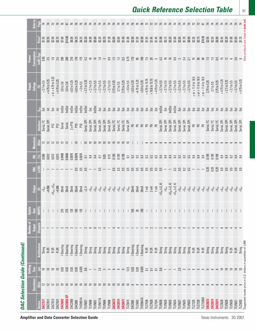
Quick Reference Selection Table 97
Amplifier and Data Converter Selection Guide Texas Instruments 3Q 2007
DAC
Sele
ctio
n Gu
ide
(Con
tinue
d)Nu
mber
ofUp
date
Supp
lyPo
wer
Settl
ing
Numb
er of
Upda
teSu
pply
Pow
erRe
solu
tion
Time
Outp
utRa
teOu
tput
DNL
INL
Mon
oton
icVo
ltage
Cons
umpt
ion
Refe
r to
Devic
e(B
its)
(µs)
Arch
itect
ure
Chan
nels
(MSP
S)(V
)(±
LSB)
(%)
(Bits
)In
terfa
ceV R
EF(V
)(m
W) (
Typ)
Pric
e*Pa
geDA
C757
112
10St
ring
1—
+VRE
F—
0.096
12Se
rial, I
2 CEx
t+ 2
.7 to
5.5
0.85
$1.55
74
DAC7
611
1210
R-2R
1—
+4.09
61
0.012
12Se
rial, S
PIIn
t+ 4
.75 to
5.25
2.5$2
.55
74DA
C761
312
10R-
2R1
—+V
REF, ±
V REF
10.0
1212
P12
Ext
±or +
4.75
to 5.
251.8
$2.50
73
DAC7
621
1210
R-2R
1—
+4.09
61
0.012
12P1
2In
t+ 4
.75 to
5.25
2.5$2
.75
74DA
C565
210
0.02
I-Ste
ering
227
520
mA1
0.048
812
Seria
lIn
t/Ext
3.0 to
3.6
290
$7.60
76
DAC5
652-
EP10
0.02
I-Ste
ering
227
520
mA1
0.048
812
Seria
lIn
t/Ext
3.0 to
3.6
290
$14.8
6 97
DAC2
900
100.0
3I-S
teer
ing2
125
20mA
10.0
976
—2 x
P10
Int/E
xt+3
.0 to
5.25
310
$6.00
76
DAC9
0010
0.03
I-Ste
ering
116
520
mA0.5
0.097
610
P10
Int/E
xt+3
.0 to
5.25
170
$4.25
76
THS5
651A
100.0
35I-S
teer
ing1
125
20mA
0.50.0
976
—P1
0In
t/Ext
+ 3 to
5.5
175
$4.25
76
TLV5
637
100.8
Strin
g2
—+2
, 4
0.50.1
10Se
rial, S
PIIn
t/Ext
+ 2.7
to 5.
254.2
$3.20
74
TLV5
608
101
Strin
g8
—+V
REF
10.4
10Se
rial, S
PIEx
t+ 2
.7 to
5.5
18$4
.90
74TL
V563
110
1St
ring
8—
+VRE
F1
0.410
Seria
l, SPI
Int/E
xt+ 2
.7 to
5.5
18$5
.60
74TL
V561
7A10
2.5St
ring
2—
+VRE
F0.5
0.110
Seria
l, SPI
Ext
+ 2.7
to 5.
51.8
$2.25
74
TLV5
604
103
Strin
g4
—+V
REF
10.0
510
Seria
l, SPI
Ext
+ 2.7
to 5.
53
$3.70
74
TLV5
606
103
Strin
g1
—+V
REF
10.1
510
Seria
l, SPI
Ext
+ 2.7
to 5.
50.9
$1.30
74
DAC6
573
109
Strin
g4
—+V
REF
0.50.1
9510
Seria
l, I2 C
Ext
2.75 t
o 5.25
1.5$3
.05
74DA
C657
410
9St
ring
4—
+VRE
F0.5
0.195
10Se
rial, I
2 CEx
t2.7
to 5.
51.5
$3.05
74
DAC6
571
109
Strin
g1
—+V
DD0.5
0.195
10Se
rial, I
2 CEx
t2.7
5 to 5
.250.5
$1.40
74
TLC5
615
1012
.5St
ring
1—
+VRE
F0.5
0.110
Seria
l, SPI
Ext
+ 4.5
to 5.
50.7
5$1
.90
74DA
C908
80.0
3I-S
teer
ing1
165
20mA
0.50.2
—P8
Ext
+3.0
to 5.
2517
0$2
.90
76TL
C560
28
0.03
I-Ste
ering
130
20mA
0.50.2
—P8
Ext
+4.75
to 5.
2580
$1.55
76
THS5
641A
80.0
35I-S
teer
ing1
100
20mA
0.50.4
—P8
Ext
+3.0
to 5.
2510
0$2
.90
76TL
C752
88
0.1R-
2R2
—1 m
A0.5
0.28
P8Ex
t+ 4
.75 to
15.75
7.5$1
.55
73TL
C762
88
0.1R-
2R2
—2 m
A0.5
0.28
P8Ex
t+ 1
0.8 to
15.75
20$1
.45
73TL
C752
48
0.1R-
2R1
—1 m
A0.5
0.28
P8Ex
t+ 4
.75 to
5.25
5$1
.45
73TL
V562
68
0.8St
ring
2—
+VRE
F (+2,
4)0.5
0.48
Seria
l, SPI
Int/E
xt+ 2
.7 to
5.5
4.2$1
.90
74TL
V562
98
1St
ring
8—
+VRE
F1
0.48
Seria
l, SPI
Ext
+ 2.7
to 5.
518
$3.15
74
TLV5
632
81
Strin
g8
—+V
REF (+
2, 4)
10.4
8Se
rial, S
PIIn
t/Ext
+ 2.7
to 5.
518
$3.35
74
TLV5
624
81
Strin
g1
—+V
REF (+
2, 4)
0.20.2
8Se
rial, S
PIIn
t/Ext
+ 2.7
to 5.
50.9
$1.60
74
TLV5
627
82.5
Strin
g4
—+V
REF
0.50.2
8Se
rial, S
PIEx
t+ 2
.7 to
5.5
3$2
.05
74TL
V562
58
3St
ring
2—
+VRE
F0.2
0.28
Seria
l, SPI
Ext
+ 2.7
to 5.
52.4
$1.70
74
TLV5
623
83
Strin
g1
—+V
REF
0.20.2
8Se
rial, S
PIEx
t+ 2
.7 to
5.5
2.1$0
.99
74TL
C722
58
5R-
2R4
—+V
REF
10.4
8P8
Ext
±or +
11.4
to 16
.575
$2.35
73
TLC7
226
85
R-2R
4—
+VRE
F1
0.48
P8Ex
t±o
r + 11
.4 to
16.5
90$2
.15
73TL
C722
6M8
5R-
2R4
—+V
REF
10.4
8P8
Ext
±or +
11.4
to 16
.590
$78.9
8 97
DAC5
573
88
Strin
g4
—+V
REF
0.25
0.195
8Se
rial, I
2 CEx
t2.7
5 to 5
.251.5
$2.55
74
DAC5
574
88
Strin
g4
—+V
REF
0.25
0.195
8Se
rial, I
2 CEx
t2.7
to 5.
51.5
$2.55
74
DAC5
571
88
Strin
g1
—+V
DD0.2
50.1
958
Seria
l, I2 C
Int
2.75 t
o 5.25
0.5$0
.90
74TL
C562
88
10St
ring
8—
+VRE
F0.9
0.48
Seria
l, SPI
Ext
+ 4.75
to 5.
2515
$2.45
74
TLV5
628
810
Strin
g8
—+V
REF
0.90.4
8Se
rial, S
PIEx
t+ 2
.7 to
5.25
12$2
.20
74TL
V562
08
10R-
2R4
—+V
REF
0.90.2
8Se
rial, S
PIEx
t+ 2
.7 to
5.5
6$1
.00
74TL
V562
18
10R-
2R4
—+V
REF
0.90.4
8Se
rial, S
PIEx
t+ 2
.7 to
5.5
3.6$1
.65
74TL
C562
08
10St
ring
4—
+VRE
F0.9
0.48
Seria
l, SPI
Ext
+ 4.75
to 5.
258
$1.75
74
* Sugg
este
d re
sale
pric
e in
U.S
. dol
lars
in q
uant
ities
of 1
,000
. N
ew p
rodu
cts
are
liste
d in
bol
d re
d.

Audio Digital-to-Analog Converters (DACs)Audio DACsPCM1780/81/82 Stereo with Volume Control, Software (1780/82) and Hardware (1781), 106 192 Normal, I2S +5 SSOP-16 $1.10
Open-Drain Output Zero Flag (1782), Improved Jitter PerformancePCM1753/54/55 Stereo with Volume Control, Software (1753/55) and Hardware (1754), Open-Drain 106 192 Normal, I2S +5 SSOP-16 $0.98
Output Zero Flag (1755)PCM1770/1 Stereo with Integrated Headphone Driver, Software (1770) and Hardware (1771) Controlled 98 48 Normal, I2S +1.6 to +3.6 TSSOP-16, $1.90
QFN-20PCM1772/3 Stereo with Integrated Line Out, Software (1772) and Hardware (1773) Controlled 98 48 Normal, I2S +1.6 to +3.6 TSSOP-16, $1.90
QFN-20PCM1738/30 Stereo Advanced Segment DAC, Soft Mute (1730), 2 Optional Operation Modes (1738): 117 192 Normal, I2S, +3.3 and +5 SSOP-28 $5.00
External Filter and DSD Decoder for SACD Playback and Digital Attenuation DSDPCM1792A Stereo, Optional DSD Format, External Filter and DSP Interface, SPI/I2C, 132 192 Standard, +3.3 and +5 SSOP-28 $13.00
Differential Current Output: 7.8mA p-p I2S, LPCM1796/8 Stereo Advanced Segment, 123dB Dynamic Range, TDMCA Serial Interface (1798) 123 192 Standard, +3.5 and +5 SSOP-28 $6.50
I2S, LPCM1606 6-Channel, Low Cost CMOS, Multilevel 103 192 Normal, I2S +5 SSOP-20 $2.48PCM1608 8-Channel, Highly Integrated DAC, Higher SNR 105 192 Normal, I2S +3.3 and +5 LQFP-48 $4.10PCM1680 8-Channel, Low Cost DAC, Improved Jitter Performance, Pin Compatible with PCM1780 103 192 Normal, I2S +5 SSOP-24 $2.60DSD1608 8-Channel, Enhanced Multiformat ∆Σ DAC, Supports DSD with TDMCA 108 192 Normal, I2S, +3.3 and +5 TQFP-52 $5.68
DSDPCM4104 4-Channel, High Performance, Sampling Rate up to 216kHz, H/W or S/W Controlled 118 216 Normal, I2S, +3.3 and +5 TQFP-48 $4.95
TDMPCM1791A Stereo Advanced Segment DAC, Optional DSD Format, External Filter and 113 192 Normal, I2S, +3.3 and +5 SSOP-28 $2.10
DSP Interface, SPI/I2C Differential Current Output: 3.2mAp-p TDMCAPCM1793 Stereo Advanced Segment DAC, Balanced Voltage Outputs, Improved Clock Jitter 113 192 Normal, I2S, +3.3 and +5 SSOP-28 $3.15
Left JustifiedTLV320DAC23 I2C and SPI Control with Headphone Amp, PDISS = 23mW 100 96 Normal, I2S, DSP +1.5 to +3.3 VFBGA-80, $2.00
TSSOP-28, QFN-28
TLV320DAC26 Integrated PLL, SPI Control, Speaker/Headphone Amp, PDISS = 11mW 97 53 Normal, I2S, DSP +2.7 to +3.6 QFN-32 $2.95TLV320DAC32 Low-Power Stereo DAC with PLL and Stereo HP/Speaker Amplifiers 95 96 Normal ,I2S, +2.7 to +3.6 QFN-32 $2.75
DSP, TDMPCM1777 Low-Power Stereo DAC with Stereo HP and Class-D Speaker Amplifiers 93 50 Normal, I2S, DSP +2.4 to +3.6 QFN-32 TBD
*Suggested resale price in U.S. dollars in quantities of 1,000. Preview products are listed in bold blue.
Amplifier and Data Converter Selection Guide Texas Instruments 3Q 2007
Quick Reference Audio Selection Tables
Data Converters
98
Audio Analog-to-Digital Converters (ADCs)Audio ADCs
Dynamic Sampling Rate Audio Data PowerDevice Description Range (dB) (kHz) (max) Format Supply (V) Package(s) Price*
PCM1850/1 Stereo ADC w/2 x 6 Input MUX and PGA, SPI (1850) and I2C (1851) Control 101 96 Normal, I2S +3.3 and +5 TQFP-32 $4.80PCM1807/8 Stereo ADC, SE Input, Mute w/Fade, SPI Control, S/W (1807) H/W (1808) Controlled 101 96 I2S, L +3.5 and +5 TSSOP-14 $1.00PCM1803A Stereo ADC, SE Input, High Pass Filter 103 96 Normal, I2S +3.5 and +5 SSOP-20 $1.10PCM1802 Stereo ADC, SE Input 105 96 Normal, I2S +3.3 and +5 SSOP-20 $3.35PCM1804 Stereo ADC, Fully Differential, High Pass Filter 112 192 Normal, I2S, DSD +3.3 and +5 SSOP-28 $3.95PCM1870 Stereo ADC, SE Input, Digital Filter, Very Low Power Consumption 90 50 Normal, I2S, DSP +2.4 and +3.6 QFN-24 $1.80PCM4204 4-Channel, High-Performance ∆Σ ADC, PCM or DSD, High Pass Filter 118 216 Normal, I2S, DSD, TDM +3.3 and +5 TQFP-64 $7.95PCM4202 Stereo, High-Performance ∆Σ ADC, PCM or DSD, High Pass Filter 118 216 Normal, I2S, DSD +3.3 and +5 SSOP-28 $4.95PCM4201 Mono, High-Performance ∆Σ ADC, PCM, High Pass Filter, 112 108 Normal, DSP +3.3 and +5 TSSOP-16 $2.50
Wide Digital Supply Range, Low Power DissipationPCM4222 2-Channel, High-Performance ∆Σ ADC 124 216 6-Bit Modulator, DSD, +3.3 and +4 TQFP-48 $14.95
Normal, I2S, TDMPCM4220 2-Channel, High-Performance ∆Σ ADC 123 216 Normal, I2S, TDM +3.3 and +4 TQFP-48 $9.95
*Suggested resale price in U.S. dollars in quantities of 1,000. New products are listed in bold red. Preview products are listed in bold blue.
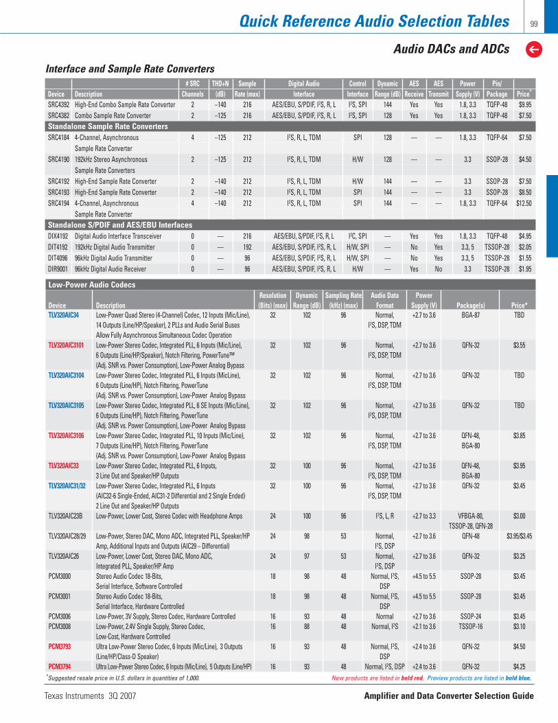
Texas Instruments 3Q 2007 Amplifier and Data Converter Selection Guide
Quick Reference Audio Selection Tables
Audio DACs and ADCs
99
Low-Power Audio CodecsResolution Dynamic Sampling Rate Audio Data Power
Device Description (Bits) (max) Range (dB) (kHz) (max) Format Supply (V) Package(s) Price*TLV320AIC34 Low-Power Quad Stereo (4-Channel) Codec, 12 Inputs (Mic/Line), 32 102 96 Normal, +2.7 to 3.6 BGA-87 TBD
14 Outputs (Line/HP/Speaker), 2 PLLs and Audio Serial Buses I2S, DSP, TDMAllow Fully Asynchronous Simultaneous Codec Operation
TLV320AIC3101 Low-Power Stereo Codec, Integrated PLL, 6 Inputs (Mic/Line), 32 102 96 Normal, +2.7 to 3.6 QFN-32 $3.556 Outputs (Line/HP/Speaker), Notch Filtering, PowerTune™ I2S, DSP, TDM(Adj. SNR vs. Power Consumption), Low-Power Analog Bypass
TLV320AIC3104 Low-Power Stereo Codec, Integrated PLL, 6 Inputs (MicLine), 32 102 96 Normal, +2.7 to 3.6 QFN-32 TBD6 Outputs (Line/HP), Notch Filtering, PowerTune I2S, DSP, TDM(Adj. SNR vs. Power Consumption), Low-Power Analog Bypass
TLV320AIC3105 Low-Power Stereo Codec, Integrated PLL, 6 SE Inputs (Mic/Line), 32 102 96 Normal, +2.7 to 3.6 QFN-32 TBD6 Outputs (Line/HP), Notch Filtering, PowerTune I2S, DSP, TDM(Adj. SNR vs. Power Consumption), Low-Power Analog Bypass
TLV320AIC3106 Low-Power Stereo Codec, Integrated PLL, 10 Inputs (Mic/Line), 32 102 96 Normal, +2.7 to 3.6 QFN-48, $3.857 Outputs (Line/HP), Notch Filtering, PowerTune I2S, DSP, TDM BGA-80(Adj. SNR vs. Power Consumption), Low-Power Analog Bypass
TLV320AIC33 Low-Power Stereo Codec, Integrated PLL, 6 Inputs, 32 100 96 Normal, +2.7 to 3.6 QFN-48, $3.953 Line Out and Speaker/HP Outputs I2S, DSP, TDM BGA-80
TLV320AIC31/32 Low-Power Stereo Codec, Integrated PLL, 6 Inputs 32 100 96 Normal, +2.7 to 3.6 QFN-32 $3.45(AIC32-6 Single-Ended, AIC31-2 Differential and 2 Single Ended) I2S, DSP, TDM2 Line Out and Speaker/HP Outputs
TLV320AIC23B Low-Power, Lower Cost, Stereo Codec with Headphone Amps 24 100 96 I2S, L, R +2.7 to 3.3 VFBGA-80, $3.00TSSOP-28, QFN-28
TLV320AIC28/29 Low-Power, Stereo DAC, Mono ADC, Integrated PLL, Speaker/HP 24 98 53 Normal, +2.7 to 3.6 QFN-48 $3.95/$3.45Amp, Additional Inputs and Outputs (AIC29 – Differential) I2S, DSP
TLV320AIC26 Low-Power, Lower Cost, Stereo DAC, Mono ADC, 24 97 53 Normal, +2.7 to 3.6 QFN-32 $3.25Integrated PLL, Speaker/HP Amp I2S, DSP
PCM3000 Stereo Audio Codec 18-Bits, 18 98 48 Normal, I2S, +4.5 to 5.5 SSOP-28 $3.45Serial Interface, Software Controlled DSP
PCM3001 Stereo Audio Codec 18-Bits, 18 98 48 Normal, I2S, +4.5 to 5.5 SSOP-28 $3.45Serial Interface, Hardware Controlled DSP
PCM3006 Low-Power, 3V Supply, Stereo Codec, Hardware Controlled 16 93 48 Normal +2.7 to 3.6 SSOP-24 $3.45PCM3008 Low-Power, 2.4V Single Supply, Stereo Codec, 16 88 48 Normal, I2S +2.1 to 3.6 TSSOP-16 $3.10
Low-Cost, Hardware ControlledPCM3793 Ultra Low-Power Stereo Codec, 6 Inputs (Mic/Line), 3 Outputs 16 93 48 Normal, I2S, +2.4 to 3.6 QFN-32 $4.50
(Line/HP/Class-D Speaker) DSPPCM3794 Ultra Low-Power Stereo Codec, 6 Inputs (Mic/Line), 5 Outputs (Line/HP) 16 93 48 Normal, I2S, DSP +2.4 to 3.6 QFN-32 $4.25
*Suggested resale price in U.S. dollars in quantities of 1,000. New products are listed in bold red. Preview products are listed in bold blue.
Interface and Sample Rate Convertersgrated Sample Rate Converters and S/PDIF – AES/EBU Transceivers
# SRC THD+N Sample Digital Audio Control Dynamic AES AES Power Pin/Device Description Channels (dB) Rate (max) Interface Interface Range (dB) Receive Transmit Supply (V) Package Price*
SRC4392 High-End Combo Sample Rate Converter 2 –140 216 AES/EBU, S/PDIF, I2S, R, L I2S, SPI 144 Yes Yes 1.8, 3.3 TQFP-48 $9.95 SRC4382 Combo Sample Rate Converter 2 –125 216 AES/EBU, S/PDIF, I2S, R, L I2S, SPI 128 Yes Yes 1.8, 3.3 TQFP-48 $7.50 Standalone Sample Rate Converters SRC4184 4-Channel, Asynchronous 4 –125 212 I2S, R, L, TDM SPI 128 — — 1.8, 3.3 TQFP-64 $7.50
Sample Rate Converter SRC4190 192kHz Stereo Asynchronous 2 –125 212 I2S, R, L, TDM H/W 128 — — 3.3 SSOP-28 $4.50
Sample Rate Converters SRC4192 High-End Sample Rate Converter 2 –140 212 I2S, R, L, TDM H/W 144 — — 3.3 SSOP-28 $7.50 SRC4193 High-End Sample Rate Converter 2 –140 212 I2S, R, L, TDM SPI 144 — — 3.3 SSOP-28 $8.50 SRC4194 4-Channel, Asynchronous 4 –140 212 I2S, R, L, TDM SPI 144 — — 1.8, 3.3 TQFP-64 $12.50
Sample Rate Converter Standalone S/PDIF and AES/EBU Interfaces DIX4192 Digital Audio Interface Transceiver 0 — 216 AES/EBU, S/PDIF, I2S, R, L I2C, SPI — Yes Yes 1.8, 3.3 TQFP-48 $4.95 DIT4192 192kHz Digital Audio Transmitter 0 — 192 AES/EBU, S/PDIF, I2S, R, L H/W, SPI — No Yes 3.3, 5 TSSOP-28 $2.05 DIT4096 96kHz Digital Audio Transmitter 0 — 96 AES/EBU, S/PDIF, I2S, R, L H/W, SPI — No Yes 3.3, 5 TSSOP-28 $1.55 DIR9001 96kHz Digital Audio Receiver 0 — 96 AES/EBU, S/PDIF, I2S, R, L H/W — Yes No 3.3 TSSOP-28 $1.95
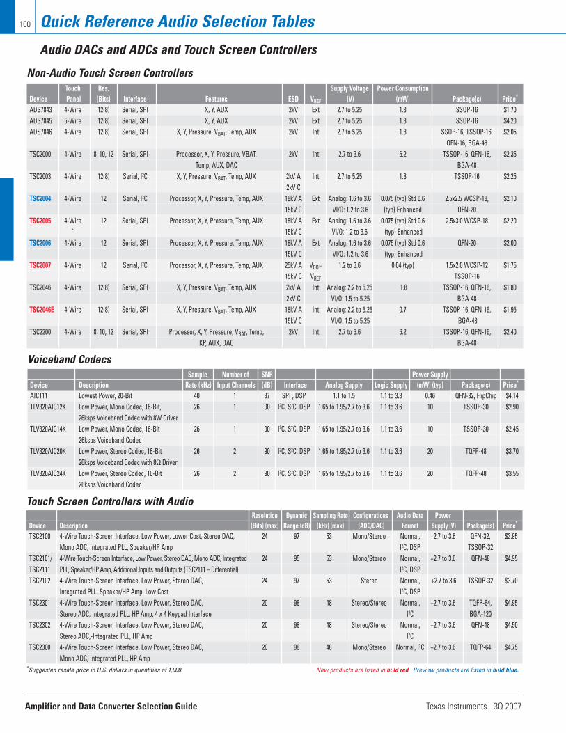
Amplifier and Data Converter Selection Guide Texas Instruments 3Q 2007
Quick Reference Audio Selection Tables
Audio DACs and ADCs and Touch Screen Controllers
100
Non-Audio Touch Screen ControllersTouch Res. Supply Voltage Power Consumption
Device Panel (Bits) Interface Features ESD VREF (V) (mW) Package(s) Price*
ADS7843 4-Wire 12(8) Serial, SPI X, Y, AUX 2kV Ext 2.7 to 5.25 1.8 SSOP-16 $1.70ADS7845 5-Wire 12(8) Serial, SPI X, Y, AUX 2kV Ext 2.7 to 5.25 1.8 SSOP-16 $4.20ADS7846 4-Wire 12(8) Serial, SPI X, Y, Pressure, VBAT, Temp, AUX 2kV Int 2.7 to 5.25 1.8 SSOP-16, TSSOP-16, $2.05
QFN-16, BGA-48TSC2000 4-Wire 8, 10, 12 Serial, SPI Processor, X, Y, Pressure, VBAT, 2kV Int 2.7 to 3.6 6.2 TSSOP-16, QFN-16, $2.35
Temp, AUX, DAC BGA-48TSC2003 4-Wire 12(8) Serial, I2C X, Y, Pressure, VBAT, Temp, AUX 2kV A Int 2.7 to 5.25 1.8 TSSOP-16 $2.25
2kV CTSC2004 4-Wire 12 Serial, I2C Processor, X, Y, Pressure, Temp, AUX 18kV A Ext Analog: 1.6 to 3.6 0.075 (typ) Std 0.6 2.5x2.5 WCSP-18, $2.10
15kV C VI/O: 1.2 to 3.6 (typ) Enhanced QFN-20TSC2005 4-Wire 12 Serial, SPI Processor, X, Y, Pressure, Temp, AUX 18kV A Ext Analog: 1.6 to 3.6 0.075 (typ) Std 0.6 2.5x3.0 WCSP-18 $2.20
` 15kV C VI/O: 1.2 to 3.6 (typ) EnhancedTSC2006 4-Wire 12 Serial, SPI Processor, X, Y, Pressure, Temp, AUX 18kV A Ext Analog: 1.6 to 3.6 0.075 (typ) Std 0.6 QFN-20 $2.00
15kV C VI/O: 1.2 to 3.6 (typ) EnhancedTSC2007 4-Wire 12 Serial, I2C Processor, X, Y, Pressure, Temp, AUX 25kV A VDD= 1.2 to 3.6 0.04 (typ) 1.5x2.0 WCSP-12 $1.75
15kV C VREF TSSOP-16TSC2046 4-Wire 12(8) Serial, SPI X, Y, Pressure, VBAT, Temp, AUX 2kV A Int Analog: 2.2 to 5.25 1.8 TSSOP-16, QFN-16, $1.80
2kV C VI/O: 1.5 to 5.25 BGA-48TSC2046E 4-Wire 12(8) Serial, SPI X, Y, Pressure, VBAT, Temp, AUX 18kV A Int Analog: 2.2 to 5.25 0.7 TSSOP-16, QFN-16, $1.95
15kV C VI/O: 1.5 to 5.25 BGA-48TSC2200 4-Wire 8, 10, 12 Serial, SPI Processor, X, Y, Pressure, VBAT, Temp, 2kV Int 2.7 to 3.6 6.2 TSSOP-16, QFN-16, $2.40
KP, AUX, DAC BGA-48
Voiceband CodecsSample Number of SNR Power Supply
Device Description Rate (kHz) Input Channels (dB) Interface Analog Supply Logic Supply (mW) (typ) Package(s) Price*
AIC111 Lowest Power, 20-Bit 40 1 87 SPI , DSP 1.1 to 1.5 1.1 to 3.3 0.46 QFN-32, FlipChip $4.14 TLV320AIC12K Low Power, Mono Codec, 16-Bit, 26 1 90 I2C, S2C, DSP 1.65 to 1.95/2.7 to 3.6 1.1 to 3.6 10 TSSOP-30 $2.90
26ksps Voiceband Codec with 8W DriverTLV320AIC14K Low Power, Mono Codec, 16-Bit 26 1 90 I2C, S2C, DSP 1.65 to 1.95/2.7 to 3.6 1.1 to 3.6 10 TSSOP-30 $2.45
26ksps Voiceband Codec TLV320AIC20K Low Power, Stereo Codec, 16-Bit 26 2 90 I2C, S2C, DSP 1.65 to 1.95/2.7 to 3.6 1.1 to 3.6 20 TQFP-48 $3.70
26ksps Voiceband Codec with 8Ω DriverTLV320AIC24K Low Power, Stereo Codec, 16-Bit 26 2 90 I2C, S2C, DSP 1.65 to 1.95/2.7 to 3.6 1.1 to 3.6 20 TQFP-48 $3.55
26ksps Voiceband Codec
Touch Screen Controllers with Audioeen Controllers with Audio
Resolution Dynamic Sampling Rate Configurations Audio Data PowerDevice Description (Bits) (max) Range (dB) (kHz) (max) (ADC/DAC) Format Supply (V) Package(s) Price*
TSC2100 4-Wire Touch-Screen Interface, Low Power, Lower Cost, Stereo DAC, 24 97 53 Mono/Stereo Normal, +2.7 to 3.6 QFN-32, $3.95Mono ADC, Integrated PLL, Speaker/HP Amp I2C, DSP TSSOP-32
TSC2101/ 4-Wire Touch-Screen Interface, Low Power, Stereo DAC, Mono ADC, Integrated 24 95 53 Mono/Stereo Normal, +2.7 to 3.6 QFN-48 $4.95TSC2111 PLL, Speaker/HP Amp, Additional Inputs and Outputs (TSC2111 – Differential) I2C, DSPTSC2102 4-Wire Touch-Screen Interface, Low Power, Stereo DAC, 24 97 53 Stereo Normal, +2.7 to 3.6 TSSOP-32 $3.70
Integrated PLL, Speaker/HP Amp, Low Cost I2C, DSPTSC2301 4-Wire Touch-Screen Interface, Low Power, Stereo DAC, 20 98 48 Stereo/Stereo Normal, +2.7 to 3.6 TQFP-64, $4.95
Stereo ADC, Integrated PLL, HP Amp, 4 x 4 Keypad Interface I2C BGA-120TSC2302 4-Wire Touch-Screen Interface, Low Power, Stereo DAC, 20 98 48 Stereo/Stereo Normal, +2.7 to 3.6 QFN-48 $4.50
Stereo ADC,-Integrated PLL, HP Amp I2CTSC2300 4-Wire Touch-Screen Interface, Low Power, Stereo DAC, 20 98 48 Mono/Stereo Normal, I2C +2.7 to 3.6 TQFP-64 $4.75
Mono ADC, Integrated PLL, HP Amp*Suggested resale price in U.S. dollars in quantities of 1,000. New products are listed in bold red. Preview products are listed in bold blue.
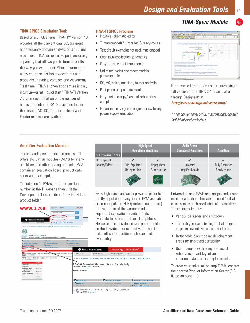
Texas Instruments 3Q 2007 Amplifier and Data Converter Selection Guide
Design and Evaluation Tools
TINA-Spice Module
101
Amplifier Evaluation Modules
To ease and speed the design process, TIoffers evaluation modules (EVMs) for manyamplifiers and other analog products. EVMscontain an evaluation board, product datasheet and user's guide.
To find specific EVMs, enter the product number at the TI website then visit theDevelopment Tools section of any individualproduct folder.
www.ti.com
High-Speed Audio PowerOperational Amplifiers Operational Amplifiers Amplifiers
Hardware ToolsDevelopment
Boards/EVMs Fully-Populated Unpopulated Universal Fully-PopulatedReady-to-Use Ready-to-Use Amplifier Boards Ready-to-use
Every high-speed and audio power amplifier hasa fully-populated, ready-to-use EVM availableor an unpopulated PCB (printed circuit board)for evaluation of the various models.Populated evaluation boards are also available for selected other TI amplifiers.Please see the individual device product folderon the TI website or contact your local TIsales office for additional choices and availability.
Universal op amp EVMs are unpopulated printedcircuit boards that eliminate the need for dual in-line samples in the evaluation of TI amplifiers.These boards feature:
• Various packages and shutdown
• The ability to evaluate single, dual, or quadamps on several eval spaces per board
• Detachable circuit board developmentareas for improved portability
• User manuals with complete boardschematic, board layout and numerous standard example circuits
To order your universal op amp EVMs, contactthe nearest Product Information Center (PIC)listed on page 119.
TINA SPICE Simulation Tool:Based on a SPICE engine, TINA-TI™ Version 7.0provides all the conventional DC, transientand frequency domain analysis of SPICE andmuch more. TINA has extensive post-processingcapability that allows you to format resultsthe way you want them. Virtual instrumentsallow you to select input waveforms andprobe circuit nodes, voltages and waveforms“real time”. TINA's schematic capture is trulyintuitive—a real "quickstart." TINA-TI Version7.0 offers no limitation on the number ofnodes or number of SPICE macromodels inthe circuit. AC, DC, Transient, Noise andFourier analysis are available.
TINA-TI SPICE Program• Intuitive schematic editor
• TI macromodels** installed & ready-to-use
• Test circuit examples for each macromodel
• Over 150+ application schematics
• Easy-to-use virtual instruments
• Unlimited nodes and macromodels per schematic
• DC, AC, noise, transient, fourier analysis
• Post-processing of data results
• Easy metafile copy/paste of schematics and plots
• Enhanced convergence engine for switching power supply simulation
For advanced features consider purchasing afull version of the TINA SPICE simulatorthrough Designsoft athttp://www.designsoftware.com/
** For conventional SPICE macromodels, consultindividual product folders.

Amplifier and Data Converter Selection Guide Texas Instruments 3Q 2007
Design and Evaluation Tools
FilterPro™, SARdriverPro™ and MDACBufferPro™
102
FilterPro: Active Filter DesignApplication FilterPro™ Multiple Feedback (MFB) andSallen-Key Design Program is a Windows®
application. This application designs MFB andSallen-Key low-pass and high-pass filtersusing voltage-feedback op amps, resistorsand capacitors. It also supports a fully-differential version of the MFB circuit. Thisprogram includes Bessell, Butterworth,Chebychev, and linear phase filter types andcan be used to design filters from 1 to 10poles. The capacitor values in each stage canbe either selected by the computer or enteredby the designer. An "always on" prompt window provides context-sensitive help information to the user. The response of thefilter is displayed on a graph, showing gain,phase and group delay over frequency.
FilterPro• Low-pass, multi-section, active filter
synthesis• High-pass, multi-section, active filter
synthesis• Multiple Feedback (MFB) topologies—
2nd order to 10th order• Sallen-Key topologies—2nd order to
10th order • Filter types:
•• Butterworth, Bessel, Chebychev, Linear• Phase, Gaussian, Custom• Manual/automatic capacitor value entry• Resistive seed value option• Schematic and final filter values display• Gain, phase, group delay response display
SARdriverPro: SAR ADC Driver Filter andOp Amp Design ApplicationSARdriverPro is a Windows application. Thisapplication is designed to choose the op ampand R-C filter (also know as charge-bucket orfly-wheel circuit) for CDAC SAR input ADCsto achieve peak performance out of the ADC.Datasheet ADC specifications and desiredsystem performance parameters are entered,R-C values computed and op amp specifica-tions calculated. When a final op amp is chosen, its parameters are entered and the R-C values optimized to match the final opamp choice based on desired overall systemperformance.
SARdriverPro• CDAC SAR ADC input drive optimizer• Input CDAC SAR specifications and
desired system performance• Output R-C values for “Charge-Bucket”
or “Fly-Wheel Circuit”• Output buffer/driver op amp specifications• Input final op amp selected specifications• Output optimized final R-C values for
desired system performance
*Expected release date 4Q 2007
MDACBufferProMDACBufferPro is a Multiplying Digital-to-Analog Converter (MDAC) design utility thatallows the designer to enter the designparameters including power supply voltage(s),output voltage range, desired MDAC deviceand other circuit parameters resulting inMDACBufferPro displaying the appropriatecircuit configuration. With the entry of thedesigner's tolerance for errors, the programcan then select an appropriate op amp.
MDACBufferPro• Library supports most output buffer optios• Enter desired output characteristics• Guidance provided based on circuit
topology and output performance required• Unipolar and Bipolar (four quadrant
multiplying) options

Texas Instruments 3Q 2007 Amplifier and Data Converter Selection Guide
Design and Evaluation Tools
Digitally Calibrated Sensor Signal Condition and 4-20mA EVMs
103
Digitally Calibrated Sensor Signal Condition and 4-20mA Evaluation Modules (EVMs)These EVMs feature hardware and/or software tools that allow for a quick start development cycle from first conceptual test drive, through firstprototype, and all the way to the first production shipment.
EVM Part No. IC Part No. Hardware Software EVM DescriptionPGA309EVM PGA309 X X Resistive bridge sensor signal conditioner. Calibration to 0.1%FSR
over temperature. Hardware and software for full temperature calibration.
XTR108EVM XTR108 X X RTD signal conditioner from 10Ω to 10kΩ RTDs. Calibration to 0.1% FSR error over RTD input range. Hardware and software for 0-5V voltage output or 4-20mA output.
SensorEmulatorEVM — X — Complete emulation of a resistive\bridge sensor over 3 temperatureranges and over 11 strain ranges (0%, 50%, 100% - Cold, 0%, 25%50%, 75%, 100% - Room, 0%, 50%,100% - Hot). Also complete emulation of bridge or absolute temperature sensor – Cold, Room,Hot
XTR300EVM XTR300 X — Surface mount part assembled plus default scaling values and ease of real world I/O interface.
XTR111EVM XTR111 X — Surface mount part assembled plus default scaling values andease of real world I/O interface
RS232
PowerSupply
+ –
VCC
GND 10nF
Customer
Sensor
PGA309
PC Interface Board
Pressure
Input
TemperatureChamber
VS
VOUT
PRG
GND
VIN
PRG
SDASCL
PGA309
Sensor Interface Board–40˚C < Temperature < +125˚C
+
–
PGA309
EEPROM
PGA309EVM + Sensor Emulator EVM =Complete Bridge Sensor Conditioning Development System
Block diagram of the PGA309EVM module.

Amplifier and Data Converter Selection Guide Texas Instruments 3Q 2007
Design and Evaluation Tools
Signal Chain Prototyping System
104
Use modular Evaluation Modules (EVMs)to prototype a complete data acquisitionsystem in minutes!
Imagine being able to prototype your entiresignal chain—input signal conditioning, A/Dconversion, processor, D/A conversion andoutput signal conditioning–with simple building blocks. Imagine not havingto lay out a printed circuit boardjust to evaluate a system signalprocessing idea.
With TI's modular EVM building blocks,you can put together a complete data acquisition system featuring signal condition-ing, an A/D converter and a processor—all injust a few minutes. For a more complete system you can add on from there—a D/Aconverter, or more output signal conditioning.With modular EVM boards that go togethereasily, thanks to standardized connectors, youcan quickly build a complete hardware prototype and get to writing your applicationcode faster.
You can also build your own modules to fitthis system, to accommodate circuits that maynot be available directly from TI. Refer to thelinks at the end of this guide to find out howthe system is defined. Get More Information:
Modular EVM Design Guidelines at:http://www-s.ti.com/sc/psheets/slaa185/slaa185.pdf
Get More Information on Modular EVMListings at: http://www.ti-estore.com/Merchant2/compatible-DSP_Analog.htm
Start with the Processor
The processor is the heart of your system. Doyou need the power of a DSP, or the featuresof a microcontroller? You're free to chooseand explore these options with the modularEVM system. The signal chain building blockshave the ability to easily snap into place onan interface card to connect them to most ofTI's DSPs.
Don't need a DSP? TI's ultra-low-powerMSP430 microcontroller products andMicroSystem Controllers feature built-in analog functionality. In many systems, external data conversion components may
be needed to complement the built-infunctions. For those cases, our broad rangeof data conversion products can be used withthese microcontrollers.
Using FPGAs instead of a processor? Some distributors of FPGAs have developedinterface boards that allow the signal chainbuilding blocks to connect to their FPGAdevelopment systems.
If you just want to evaluate the device on the EVM using standard lab equipment, orwant to try wiring the board into your existing system, the modular EVMs will allow for that as well, no processor needed.You have access to all the essential interfacepins on the device through the standardizedconnectors. So no matter how you processthe data, we've got a way to help you develop your system.
Ready to Get Started?
If you've decided to use a DSP in your system, an interface card may be required toconnect your DSP Starter Kit (DSK) to themodular EVMs. Refer to the table at the endof this article to see which interface isrequired for your DSK. A listing of EVMs compatible with our DSKs can be found onthe TI eStore. www.ti-estore.com
If the TMS470 microcontroller is what youare using, the TMS470 System DevelopmentBoard was designed to fit on the HPA-MCUInterface Board.
Developing with Modular EVMs
Developing software with the modularEVMs is easy. If you're using a DSP,
our free Data Converter SupportPlug-In for Code Composer Studio™
Studio integrated development environ-ment (IDE) can help you set up the DSP to
interface with the data converters.
If you are developing TMS470 code with IAREmbedded Workbench, you can use the JlinkUSB-JTAG Debugger to download programsto the TMS470R1B1M.
Code Examples
Code for use with the modular EVMs on thedifferent platforms can be found in the toolfolder for the EVM. Look for the RelatedSoftware section in Related Documents inthe tool folder. Very often, this code is a simple project that runs on the processorused; in some cases, complete software toevaluate data converters that runs on your PC is included as well.
The data converter support plug-in residing inTI’s Code Composer Studio IDE makes it easierthan ever to design with TI data converterproducts along with TI’s TMS320™ digital signal processors (DSPs).
Using the free tool in the Code ComposerStudio IDE reduces the time required to configure data converters by up to 90 percent.The plug-in software module generates initialization data and interface software forthe user’s data converter/DSP combinationusing a graphical user interface, along withthe necessary data structures. For many dataconverter EVMs and DSP Starter Kit (DSK)combinations, complete software examplescontaining source code and pre-coded executables to run the data converter areavailable. The software examples show howto design with the data converter by usingthe interface software generated by the dataconverter plug-in module (DCP).
Software Saves Configuration Time
Today, state-of-the-art data converters arehighly integrated, requiring configuration forinput channel selection, filters, interfaces,

Texas Instruments 3Q 2007 Amplifier and Data Converter Selection Guide
Design and Evaluation Tools
Resources
105
adjustable gain control, offset cancellation,integrated first-in-first-out (FIFO) memory andother features. Creating data converter interface software can complicate the development effort. TI data converters andthe interface software simplify the softwaredevelopment task, reducing time-to-marketfor applications using TI DSPs.
The DCP is a component of TI’s industry-lead-ing Code Composer Studio IDE and offerseasy-to-use windows for “point-and-click”configuration, preventing illegal combinationsof settings. The DCP automatically createsthe interface software as the C source codenecessary to use the data converter, theninserts the code into the existing user project. The created files contain the functions necessary to initialize the data converter, read/write sample values and toperform special functions (like power-down).
Innovations in Design Support
TI merges DSP hardware, DSP software anddata converters to simplify the designprocess with a comprehensive DSP solutionthat includes peripherals.
Support is available for data converters usedwith TI’s C28x™, C54x™ , C55x™, C62x™,C64x™ and C67x™ DSP generations.
The easy-to-use support software benefitsdevelopers of wireless data networking,portable audio, voice-over-packet, digitalimaging, speech, motor control and a widerange of other advanced DSP-based applications.
The software has been fully tested in conjunction with the DSK and the data converter EVMs. Help files are included alongwith the data converter information in theplug-in module. These features minimize riskand ease the learning curve so the DSPdesigners can start system developmentquickly, concentrating their efforts in areas ofproduct innovation to improve the value oftheir intellectual property and get the greatestreturn of investment.
Using TI’s Data Converter InterfaceSoftware
TI is committed to complementing its DSPswith a full range of data converters. Interfacesoftware for new DSP-optimized TI data converter products is planned, includingDACs and ADCs, as well as codecs andselected special function devices.
The DCP module and the already availabledata converter software for more than 125data converters is included with the CodeComposer Studio IDE. To order CodeComposer Studio IDE, visit our web page atdspvillage.ti.com
As new interface software is developed, itwill be made available as part of the DCPmodule. The new versions can be down-loaded and installed in the Code ComposerStudio IDE, versions 2.0 and higher.
Updates to the DCP module can be downloaded free of charge fromwww.ti.com/dcplug-in
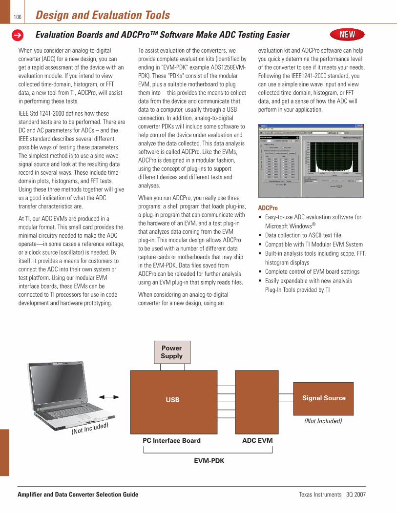
Amplifier and Data Converter Selection Guide Texas Instruments 3Q 2007
Design and Evaluation Tools
Evaluation Boards and ADCPro™ Software Make ADC Testing Easier
106
When you consider an analog-to-digitalconverter (ADC) for a new design, you canget a rapid assessment of the device with anevaluation module. If you intend to viewcollected time-domain, histogram, or FFTdata, a new tool from TI, ADCPro, will assistin performing these tests.
IEEE Std 1241-2000 defines how thesestandard tests are to be performed. There areDC and AC parameters for ADCs – and theIEEE standard describes several differentpossible ways of testing these parameters.The simplest method is to use a sine wavesignal source and look at the resulting datarecord in several ways. These include timedomain plots, histograms, and FFT tests.Using these three methods together will giveus a good indication of what the ADCtransfer characteristics are.
At TI, our ADC EVMs are produced in amodular format. This small card provides theminimal circuitry needed to make the ADCoperate—in some cases a reference voltage,or a clock source (oscillator) is needed. Byitself, it provides a means for customers toconnect the ADC into their own system ortest platform. Using our modular EVMinterface boards, these EVMs can beconnected to TI processors for use in codedevelopment and hardware prototyping.
To assist evaluation of the converters, weprovide complete evaluation kits (identified byending in "EVM-PDK" example ADS1258EVM-PDK). These "PDKs" consist of the modularEVM, plus a suitable motherboard to plugthem into—this provides the means to collectdata from the device and communicate thatdata to a computer, usually through a USBconnection. In addition, analog-to-digitalconverter PDKs will include some software tohelp control the device under evaluation andanalyze the data collected. This data analysissoftware is called ADCPro. Like the EVMs,ADCPro is designed in a modular fashion,using the concept of plug-ins to supportdifferent devices and different tests andanalyses.
When you run ADCPro, you really use threeprograms: a shell program that loads plug-ins,a plug-in program that can communicate withthe hardware of an EVM, and a test plug-inthat analyzes data coming from the EVMplug-in. This modular design allows ADCProto be used with a number of different datacapture cards or motherboards that may shipin the EVM-PDK. Data files saved fromADCPro can be reloaded for further analysisusing an EVM plug-in that simply reads files.
When considering an analog-to-digitalconverter for a new design, using an
evaluation kit and ADCPro software can helpyou quickly determine the performance levelof the converter to see if it meets your needs.Following the IEEE1241-2000 standard, youcan use a simple sine wave input and viewcollected time-domain, histogram, or FFTdata, and get a sense of how the ADC willperform in your application.
ADCPro• Easy-to-use ADC evaluation software for
Microsoft Windows®
• Data collection to ASCII text file• Compatible with TI Modular EVM System• Built-in analysis tools including scope, FFT,
histogram displays• Complete control of EVM board settings• Easily expandable with new analysis
Plug-In Tools provided by TI
Power
Supply
PC Interface Board ADC EVM
(Not Included)
(Not Included)
EVM-PDK
USB Signal Source
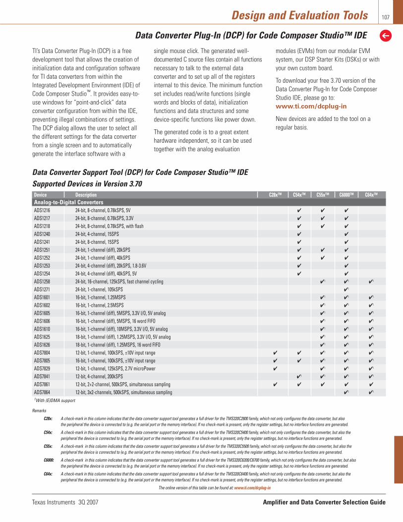
Texas Instruments 3Q 2007 Amplifier and Data Converter Selection Guide
Design and Evaluation Tools
Data Converter Plug-In (DCP) for Code Composer Studio™ IDE
107
TI’s Data Converter Plug-In (DCP) is a freedevelopment tool that allows the creation ofinitialization data and configuration softwarefor TI data converters from within theIntegrated Development Environment (IDE) ofCode Composer Studio™. It provides easy-to-use windows for “point-and-click” data converter configuration from within the IDE, preventing illegal combinations of settings.The DCP dialog allows the user to select allthe different settings for the data converterfrom a single screen and to automaticallygenerate the interface software with a
single mouse click. The generated well-documented C source files contain all functionsnecessary to talk to the external data converter and to set up all of the registersinternal to this device. The minimum functionset includes read/write functions (singlewords and blocks of data), initialization functions and data structures and somedevice-specific functions like power down.
The generated code is to a great extent hardware independent, so it can be usedtogether with the analog evaluation
modules (EVMs) from our modular EVM system, our DSP Starter Kits (DSKs) or withyour own custom board.
To download your free 3.70 version of theData Converter Plug-In for Code ComposerStudio IDE, please go to: www.ti.com/dcplug-in
New devices are added to the tool on a regular basis.
Data Converter Support Tool (DCP) for Code Composer Studio™ IDESupported Devices in Version 3.70 Device Description C28x™ C54x™ C55x™ C6000™ C64x™Analog-to-Digital ConvertersADS1216 24-bit, 8-channel, 0.78kSPS, 5V
ADS1217 24-bit, 8-channel, 0.78kSPS, 3.3V
ADS1218 24-bit, 8-channel, 0.78kSPS, with flash
ADS1240 24-bit, 4-channel, 15SPS
ADS1241 24-bit, 8-channel, 15SPS
ADS1251 24-bit, 1-channel (diff), 20kSPS
ADS1252 24-bit, 1-channel (diff), 40kSPS
ADS1253 24-bit, 4-channel (diff), 20kSPS, 1.8-3.6V
ADS1254 24-bit, 4-channel (diff), 40kSPS, 5V
ADS1258 24-bit, 16-channel, 125kSPS, fast channel cycling 1 1 1
ADS1271 24-bit, 1-channel, 105kSPS 1
ADS1601 16-bit, 1-channel, 1.25MSPS 1 1 1
ADS1602 16-bit, 1-channel, 2.5MSPS 1 1 1
ADS1605 16-bit, 1-channel (diff), 5MSPS, 3.3V I/O, 5V analog 1 1 1
ADS1606 16-bit, 1-channel (diff), 5MSPS, 16 word FIFO 1 1 1
ADS1610 16-bit, 1-channel (diff), 10MSPS, 3.3V I/O, 5V analog 1 1 1
ADS1625 18-bit, 1-channel (diff), 1.25MSPS, 3.3V I/O, 5V analog 1 1 1
ADS1626 18-bit, 1-channel (diff), 1.25MSPS, 16 word FIFO 1 1 1
ADS7804 12-bit, 1-channel, 100kSPS, ±10V input range 1 1 1
ADS7805 16-bit, 1-channel, 100kSPS, ±10V input range 1 1 1
ADS7829 12-bit, 1-channel, 125kSPS, 2.7V microPower 1 1 1
ADS7841 12-bit, 4-channel, 200kSPS 1 1 1 1
ADS7861 12-bit, 2+2-channel, 500kSPS, simultaneous sampling
ADS7864 12-bit, 3x2-channels, 500kSPS, simultaneous sampling 1 1
1With (E)DMA supportDevice Description C28x™ C54x™ C55x™ C6000™
Remarks
C28x: A check-mark in this column indicates that the data converter support tool generates a full driver for the TMS320C2800 family, which not only configures the data converter, but also the peripheral the device is connected to (e.g. the serial port or the memory interface). If no check-mark is present, only the register settings, but no interface functions are generated.
C54x: A check-mark in this column indicates that the data converter support tool generates a full driver for the TMS320C5400 family, which not only configures the data converter, but also the peripheral the device is connected to (e.g. the serial port or the memory interface). If no check-mark is present, only the register settings, but no interface functions are generated.
C55x: A check-mark in this column indicates that the data converter support tool generates a full driver for the TMS320C5500 family, which not only configures the data converter, but also the peripheral the device is connected to (e.g. the serial port or the memory interface). If no check-mark is present, only the register settings, but no interface functions are generated.
C6000: A check-mark in this column indicates that the data converter support tool generates a full driver for the TMS320C6200/C6700 family, which not only configures the data converter, but also the peripheral the device is connected to (e.g. the serial port or the memory interface). If no check-mark is present, only the register settings, but no interface functions are generated.
C64x: A check-mark in this column indicates that the data converter support tool generates a full driver for the TMS320C6400 family, which not only configures the data converter, but also the peripheral the device is connected to (e.g. the serial port or the memory interface). If no check-mark is present, only the register settings, but no interface functions are generated.
The online version of this table can be found at: www.ti.com/dcplug-in

Amplifier and Data Converter Selection Guide Texas Instruments 3Q 2007
Design and Evaluation Tools
Data Converter Plug-In (DCP) for Code Composer Studio™ IDE
108
Remarks
C28x: A check-mark in this column indicates that the data converter support tool generates a full driver for the TMS320C2800 family, which not only configures the data converter, but also the peripheral the device is connected to (e.g. the serial port or the memory interface). If no check-mark is present, only the register settings, but no interface functions are generated.
C54x: A check-mark in this column indicates that the data converter support tool generates a full driver for the TMS320C5400 family, which not only configures the data converter, but also the peripheral the device is connected to (e.g. the serial port or the memory interface). If no check-mark is present, only the register settings, but no interface functions are generated.
C55x: A check-mark in this column indicates that the data converter support tool generates a full driver for the TMS320C5500 family, which not only configures the data converter, but also the peripheral the device is connected to (e.g. the serial port or the memory interface). If no check-mark is present, only the register settings, but no interface functions are generated.
C6000: A check-mark in this column indicates that the data converter support tool generates a full driver for the TMS320C6200/C6700 family, which not only configures the data converter, but also the peripheral the device is connected to (e.g. the serial port or the memory interface). If no check-mark is present, only the register settings, but no interface functions are generated.
C64x: A check-mark in this column indicates that the data converter support tool generates a full driver for the TMS320C6400 family, which not only configures the data converter, but also the peripheral the device is connected to (e.g. the serial port or the memory interface). If no check-mark is present, only the register settings, but no interface functions are generated.
The online version of this table can be found at: www.ti.com/dcplug-in
Device Description C28x™ C54x™ C55x™ C6000™ C64x™Analog-to-Digital Converters (Continued):ADS7881 12-bit, 1-channel, 4MSPS , internal reference 1 1 1
ADS7891 14-bit, 1-channel, 3MSPS, internal reference 1 1 1
ADS803 12-bit, 1-channel, 5MSPS 1 1 1
ADS804 12-bit, 1-channel, 10MSPS 1 1 1
ADS805 12-bit, 1-channel, 20MSPS 1 1 1
ADS8320 16-bit, 1-channel, 100kSPS, 2.7-5.25V 1 1 1
ADS8321 16-bit, 1-channel, 100kSPS, 4.75-5.25V 1 1 1
ADS8322 16-bit, 1-channel (diff), 500kSPS, 5V 1 1 1
ADS8323 16-bit, 1-channel (diff), 500kSPS, 5V 1 1 1
ADS8324 14-bit, 1-channel, 50kSPS, 1.8-3.6V 1 1 1
ADS8325 16-bit, 1-channel, 100kSPS, 2.7-5.5V 1 1 1
ADS8361 16-bit, 2+2-channel, 500kSPS, simultaneous sampling
ADS8364 16-bit, 6-channel, 250kSPS
ADS8370 16-bit, 1-channel, 600kSPS, unipolar pseudo diff, internal reference 1 1 1
ADS8371 16-bit, 1-channel, 750kSPS, unipolar input, micro power 1 1 1
ADS8372 16-bit, 1-channel (diff), 600kSPS, pseudo bipolar, internal reference 1 1 1
ADS8380 18-bit, 1-channel, 600kSPS, unipolar pseudo diff, internal reference 1 1 1
ADS8381 18-bit, 1-channel, 580kSPS 1 1 1
ADS8382 18-bit, 1-channel (diff), 600kSPS, pseudo bipolar, internal reference 1 1 1
ADS8383 18-bit, 1-channel, 500kSPS 1 1 1
ADS8401 16-bit, 1-channel, 1.25MSPS, unipolar input 1 1 1
ADS8402 16-bit, 1-channel, 1.25MSPS, bipolar input 1 1 1
ADS8405 16-bit, 1-channel, 1.25MSPS, unipolar input 1 1 1
ADS8406 16-bit, 1-channel, 1.25MSPS, bipolar input 1 1 1
ADS8411 16-bit, 1-channel, 2MSPS, unipolar input 1 1 1
ADS8412 16-bit, 1-channel, 2MSPS, bipolar input 1 1 1
ADS8422 16-bit, 1-channel, 4MSPS, pseudo bipolar, differential input 1 1 1
ADS8481 18-bit, 1-channel, 1MSPS, pseudo differential, unipolar input 1 1 1
ADS8482 18-bit, 1-channel, 1MSPS, pseudo bipolar, fully differential 1 1 1
ADS8504 12-bit, 1-channel, 250kSPS, ±10V input range 1 1 1
ADS8505 16-bit, 1-channel, 250kSPS, ±10V input range 1 1 1
PCM1804 24-bit, stereo, 192kHz, audio ADC 1 1
PCM4202 24-bit, stereo, 192kHz, audio ADC 1 1
PCM4204 24-bit, 4-channel, 216kHz, audio ADC 1
THS10064 10-bit, 4-channel, 6MSPS, 16 word FIFO 1 1 1
THS1007 10-bit, 4-channel, 8MSPSTHS10082 10-bit, 2-channel, 8MSPS, 16 word FIFO 1 1 1
THS1009 10-bit, 2-channel, 8MSPSTHS1206 12-bit, 4-channel, 6MSPS, 16 word FIFO 1 1 1
THS1207 12-bit, 4-channel, 8MSPSTHS12082 12-bit, 2-channel, 8MSPS, 16 word FIFO 1 1 1
THS1209 12-bit, 2-channel, 8MSPS1With (E)DMA support Device Description
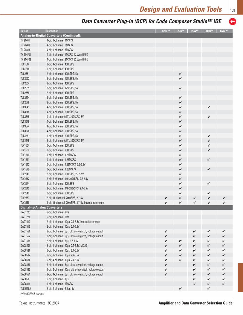
Texas Instruments 3Q 2007 Amplifier and Data Converter Selection Guide
Design and Evaluation Tools
Data Converter Plug-In (DCP) for Code Composer Studio™ IDE
109
Device Description C28x™ C54x™ C55x™ C6000™ C64x™Analog-to-Digital Converters (Continued):THS1401 14-bit, 1-channel, 1MSPSTHS1403 14-bit, 1-channel, 3MSPSTHS1408 14-bit, 1-channel, 8MSPSTHS14F01 14-bit, 1-channel, 1MSPS, 32 word FIFOTHS14F03 14-bit, 1-channel, 3MSPS, 32 word FIFOTLC1514 10-bit, 4-channel, 400kSPSTLC1518 10-bit, 8-channel, 400kSPSTLC2551 12-bit, 1-channel, 400kSPS, 5V
TLC2552 12-bit, 2-channel, 175kSPS, 5V
TLC2554 12-bit, 4-channel, 400kSPSTLC2555 12-bit, 1-channel, 175kSPS, 5V
TLC2558 12-bit, 8-channel, 400kSPSTLC2574 12-bit, 4-channel, 200kSPS, 5V
TLC2578 12-bit, 8-channel, 200kSPS, 5V
TLC3541 14-bit, 1-channel, 200kSPS, 5V
TLC3544 14-bit, 4-channel, 200kSPS, 5V
TLC3545 14-bit, 1-channel (diff), 200kSPS, 5V
TLC3548 14-bit, 8-channel, 200kSPS, 5V
TLC3574 14-bit, 4-channel, 200kSPS, 5V
TLC3578 14-bit, 8-channel, 200kSPS, 5V
TLC4541 16-bit, 1-channel, 200kSPS, 5V
TLC4545 16-bit, 1-channel (diff), 200kSPS, 5V
TLV1504 10-bit, 4-channel, 200kSPS
TLV1508 10-bit, 8-channel, 200kSPS
TLV1570 10-bit, 8-channel, 1.25MSPS
TLV1571 10-bit, 1-channel, 1.25MSPS 1
TLV1572 10-bit, 1-channel, 1.25MSPS, 2.5-5.5V
TLV1578 10-bit, 8-channel, 1.25MSPS 1
TLV2541 12-bit, 1-channel, 200kSPS, 2.7-5.5V
TLV2542 12-bit, 2-channel, 140-200kSPS, 2.7-5.5V
TLV2544 12-bit, 4-channel, 200kSPS 1
TLV2545 12-bit, 1-channel, 140-200kSPS, 2.7-5.5V
TLV2548 12-bit, 8-channel, 200kSPS 1
TLV2553 12-bit, 11-channel, 200kSPS, 2.7-5V
TLV2556 12-bit, 11-channel, 200kSPS, 2.7-5V, internal reference
Digital-to-Analog ConvertersDAC1220 16-bit, 1-channel, 2msDAC1221 16-bit, 1-channel, 2msDAC7512 12-bit, 1-channel, 10µs, 2.7-5.5V, internal referenceDAC7513 12-bit, 1-channel, 10µs, 2.7-5.5VDAC7551 12-bit, 1-channel, 5µs, ultra-low glitch, voltage output 1 1 1
DAC7552 12-bit, 2-channel, 5µs, ultra-low glitch, voltage output 1 1 1
DAC7554 12-bit, 4-channel, 5µs, 2.7-5.5V 1 1 1 1
DAC8501 16-bit, 1-channel, 10µs, 2.7-5.5V, MDAC 1 1 1
DAC8531 16-bit, 1-channel, 10µs, 2.7-5.5V 1 1 1
DAC8532 16-bit, 2-channel, 10µs, 2.7-5.5V 1 1 1
DAC8534 16-bit, 4-channel, 10µs, 2.7-5.5V 1 1 1
DAC8551 16-bit, 1-channel, 5µs, ultra-low glitch, voltage output 1 1 1
DAC8552 16-bit, 2-channel, 10µs, ultra-low glitch, voltage output 1 1 1
DAC8554 12-bit, 4-channel, 5µs, ultra-low glitch, voltage output 1 1 1
DAC8580 16-bit, 1-channel, 1µs 1 1 1
DAC8814 16-bit, 4-channel, 2MSPS 1 1
TLC5618A 12-bit, 2-channel, 2.5µs, 5V 2
1With (E)DMA support Device Description
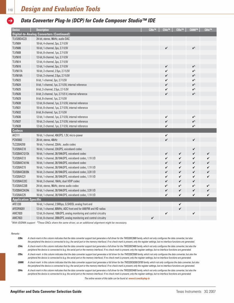
Amplifier and Data Converter Selection Guide Texas Instruments 3Q 2007
Design and Evaluation Tools
Data Converter Plug-In (DCP) for Code Composer Studio™ IDE
110
Device Description C28x™ C54x™ C55x™ C6000™ C64x™Digital-to-Analog Converters (Continued):TLV320DAC23 24-bit, stereo, 96kHz, audio DACTLV5604 10-bit, 4-channel, 3µs, 2.7-5.5VTLV5606 10-bit, 1-channel, 3µs, 2.7-5.5V 2
TLV5608 10-bit, 8-channel, 1µs, 2.7-5.5VTLV5610 12-bit, 8-channel, 1µs, 2.7-5.5VTLV5614 12-bit, 4-channel, 3µs, 2.7-5.5VTLV5616 12-bit, 1-channel, 3µs, 2.7-5.5V 2
TLV5617A 10-bit, 2-channel, 2.5µs, 2.7-5.5V 2
TLV5618A 12-bit, 2-channel, 2.5µs, 2.7-5.5V 2
TLV5623 8-bit, 1-channel, 3µs, 2.7-5.5V 2
TLV5624 8-bit, 1-channel, 1µs, 2.7-5.5V, internal reference 2
TLV5625 8-bit, 2-channel, 2.5µs, 2.7-5.5V 2
TLV5626 8-bit, 2-channel, 1µs, 2.7-5.5 V, internal reference 2
TLV5629 8-bit, 8-channel, 1µs, 2.7-5.5VTLV5630 12-bit, 8-channel, 1µs, 2.7-5.5V, internal referenceTLV5631 10-bit, 8-channel, 1µs, 2.7-5.5V, internal referenceTLV5632 8-bit, 8-channel, 1µs, 2.7-5.5VTLV5636 12-bit, 1-channel, 1µs, 2.7-5.5V, internal reference 2
TLV5637 10-bit, 2-channel, 1µs, 2.7-5.5V, internal reference 2
TLV5638 12-bit, 2-channel, 1µs, 2.7-5.5V, internal reference 2
CodecsAIC111 16-bit, 1-channel, 40kSPS, 1.3V, micro-power
PCM3002 20-bit, stereo, 48kHz
TLC320AD50 16-bit, 1-channel, 22kHz , audio codecTLV320AIC10 16-bit, 1-channel, 22kSPS, voiceband codec
TLV320AIC12/12k 16-bit, 1-channel, 26/104kSPS, voiceband codec
TLV320AIC13 16-bit, 1-channel, 26/104kSPS, voiceband codec, 1.1V I/O
TLV320AIC14/14k 16-bit, 1-channel, 26/104kSPS, voiceband codec
TLV320AIC15 16-bit, 1-channel, 26/104kSPS, voiceband codec, 1.1V I/O
TLV320AIC20/20k 16-bit, 2-channel, 26/104kSPS, voiceband codec, 3.3V I/O
TLV320AIC21 16-bit, 1-channel, 26/104kSPS, voiceband codec, 1.1V I/O
TLV320AIC22C 16-bit, 2-channel, 16kHz, dual VOIP codec
TLV320AIC23B 24-bit, stereo, 96kHz, stereo audio codec 1 1 1 1
TLV320AIC24/24k 16-bit, 1-channel, 26/104kSPS, voiceband codec, 3.3V I/O
TLV320AIC25 16-bit, 1-channel, 26/104kSPS, voiceband codec, 1.1V I/O
Application SpecificAFE1230 16-bit, 1-channel, 2.5Mbps, G.SHDSL analog front end
AFEDRI8201 12-bit, 1-channel, 80MHz, ADC front end for AM/FM and HD radios
AMC7820 12-bit, 8-channel, 100kSPS, analog monitoring and control circuitry
AMC7823 12-bit, 8-channel, 200kSPS, analog monitoring and control circuitry 1With (E)DMA support 2These DACs share the same driver, so an additional alignment might be necessary.
Remarks
C28x: A check-mark in this column indicates that the data converter support tool generates a full driver for the TMS320C2800 family, which not only configures the data converter, but also the peripheral the device is connected to (e.g. the serial port or the memory interface). If no check-mark is present, only the register settings, but no interface functions are generated.
C54x: A check-mark in this column indicates that the data converter support tool generates a full driver for the TMS320C5400 family, which not only configures the data converter, but also the peripheral the device is connected to (e.g. the serial port or the memory interface). If no check-mark is present, only the register settings, but no interface functions are generated.
C55x: A check-mark in this column indicates that the data converter support tool generates a full driver for the TMS320C5500 family, which not only configures the data converter, but also the peripheral the device is connected to (e.g. the serial port or the memory interface). If no check-mark is present, only the register settings, but no interface functions are generated.
C6000: A check-mark in this column indicates that the data converter support tool generates a full driver for the TMS320C6200/C6700 family, which not only configures the data converter, but also the peripheral the device is connected to (e.g. the serial port or the memory interface). If no check-mark is present, only the register settings, but no interface functions are generated.
C64x: A check-mark in this column indicates that the data converter support tool generates a full driver for the TMS320C6400 family, which not only configures the data converter, but also the peripheral the device is connected to (e.g. the serial port or the memory interface). If no check-mark is present, only the register settings, but no interface functions are generated.
The online version of this table can be found at: www.ti.com/dcplug-in
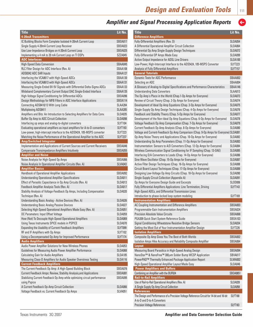
Texas Instruments 3Q 2007 Amplifier and Data Converter Selection Guide
Design and Evaluation Tools
Amplifier and Signal Processing Application Reports
111
Title Lit No.4-20mA TransmittersIC Building Blocks Form Complete Isolated 4-20mA Current-Loop SBOA017Single Supply 4-20mA Current Loop Receiver SBOA023Use Low-Impedance Bridges on 4-20mA Current Loop SBOA025Implementing a 4 mA to 20 mA Current Loop on TI DSPs SZZA045ADC Interfaces High-Speed Data Conversion SBAA045RLC Filter Design for ADC Interface (Rev. A) SBAA108ADS8342 ADC SAR Inputs SBAA127Interfacing the VCA8617 with High-Speed ADCs SBAA130Interfacing the VCA8613 with High-Speed ADCs SBAA131Measuring Single-Ended 0V-5V Signals with Differential Delta-Sigma ADCs SBAA133Wideband Complementary Current Output DAC Single-Ended Interface SBAA135High-Voltage Signal Conditioning for Differential ADCs SBOA096Design Methodology for MFB Filters in ADC Interface Applications SBOA114Connecting ADS8410/13 With Long Cable SLAA284Multiplexing ADS8411 SLAA285Amplifiers and Bits: An Introduction to Selecting Amplifiers for Data Conv. SLOA035Buffer Op Amp to ADC Circuit Collection SLOA098Interfacing op amps and analog-to-digital converters SLYT104Evaluating operational amplifiers as input amplifiers for A-to-D converters SLYT193Low-power, high-intercept interface to the ADS5424, 105-MSPS converter SLYT223Matching the Noise Performance of the Operational Amplifier to the ADC SLYT237Amp/Switched IntegratorImplementation and Applications of Current Sources and Current Receivers SBOA046Compensate Transimpedance Amplifiers Intuitively SBOA055Amplifier and NoiseNoise Analysis for High-Speed Op Amps SBOA066Noise Analysis In Operational Amplifier Circuits (Rev. A) SLVA043Amplifier BasicsHandbook of Operational Amplifier Applications SBOA092Understanding Operational Amplifier Specifications SLOA011Effect of Parasitic Capacitance in Op Amp Circuits (Rev. A) SLOA013Feedback Amplifier Analysis Tools (Rev. A) SLOA017Stability Analysis of Voltage-Feedback Op Amps, Including Compensation SLOA020Technique (Rev. A) Understanding Basic Analog - Active Devices (Rev. A) SLOA026Understanding Basic Analog Passive Devices SLOA027Selecting High-Speed Operational Amplifiers Made Easy (Rev. A) SLOA051DC Parameters: Input Offset Voltage SLOA059How (Not) To Decouple High-Speed Operational Amplifiers SLOA069Using Texas Instruments SPICE models in PSPICE SLOA070Expanding the Usability of Current-Feedback Amplifiers SLYT099RF and IF Amplifiers with Op Amps SLYT102Using a Decompensated Op Amp for Improved Performance SLYT174Audio AmplifiersAudio Power Amplifier Solutions for New Wireless Phones SLOA053Guidelines for Measuring Audio Power Amplifier Performance SLOA068Calculating Gain for Audio Amplifiers SLOA105Measuring Class-D Amplifiers for Audio Speaker Overstress Testing SLOA116Current-Feedback AmplifiersThe Current-Feedback Op Amp: A High-Speed Building Block SBOA076Current Feedback Amps: Review, Stability Analysis,and Applications SBOA081Stabilizing Current-Feedback Op Amp while optimizing circuit performance SBOA095using PspiceA Current Feedback Op-Amp Circuit Collection SLOA066Voltage Feedback vs. Current Feedback Op Amps SLVA051
Title Lit No.Difference AmplifiersFully-Differential Amplifiers (Rev. D) SLOA054A Differential Operational Amplifier Circuit Collection SLOA064Differential Op Amp Single-Supply Design Techniques SLOA072Fully-Differential OP Amps Made Easy SLOA099Active Output Impedance for ADSL Line Drivers SLOA100Low-Power, High-Intercept Interface to the ADS5424, 105-MSPS Converter SLYT223Analysis of Fully Differential Amplifiers SLYT157General TutorialsDynamic Tests for ADC Performance SBAA002Selecting an ADC SBAA004A Glossary of Analog-to-Digital Specifications and Performance Characteristics SBAA146Understanding Data Converters SLAA013The Op Amp's Place in the World (Chap.1-Op Amps for Everyone) SLOA073Review of Circuit Theory (Chap. 2-Op Amps for Everyone) SLOA074Development of Ideal Op Amp Equations (Chap. 3-Op Amps for Everyone) SLOA075Single-Supply Op Amp Design Techniques (Chap. 4-Op Amps for Everyone) SLOA076Feedback and Stability Theory (Chap. 5-Op Amps for Everyone) SLOA077Development of the Non-Ideal Op Amp Equations (Chap. 6-Op Amps for Everyone) SLOA078Voltage Feedback Op Amp Compensation (Chap. 7-Op Amps for Everyone) SLOA079Current Feedback Op Amp Analysis (Chap. 8-Op Amps for Everyone) SLOA080Voltage and Current-Feedback Op Amp Comparison (Chap. 9-Op Amps for Everyone) SLOA081Op Amp Noise Theory and Applications (Chap. 10-Op Amps for Everyone) SLOA082Understanding Op Amp Parameters (Chap. 11-Op Amps for Everyone) SLOA083Instrumentation: Sensors to A/D Converters (Chap. 12-Op Amps for Everyone) SLOA084Wireless Communication Signal Conditioning for IF Sampling (Chap. 13-OAE) SLOA085Interfacing D/A Converters to Loads (Chap. 14-Op Amps for Everyone) SLOA086Sine Wave Oscillator (Chap. 15-Op Amps for Everyone) SLOA087Active Filter Design Techniques (Chap. 16-Op Amps for Everyone) SLOA088Circuit Board Layout Techniques (Chap. 17-Op Amps for Everyone) SLOA089Designing Low-Voltage Op Amp Circuits (Chap. 18-Op Amps for Everyone) SLOA090Single-Supply Circuit Collection (Appendix A) SLOA091Op Amps for Everyone Design Guide and Excerpts SLOD006Fully Differential Amplifiers Applications: Line Termination, Driving SLYT143High-Speed ADCs, and Differential Transmission LinesIntroduction to phase-locked loop system modeling SLYT169Instrumentation AmplifiersAC Coupling Instrumentation and Difference Amplifiers SBOA003Programmable-Gain Instrumentation Amplifiers SBOA024Precision Absolute Value Circuits SBOA068PGA309 Quick Start System Reference Guide SBOA103Signal Conditioning Wheatstone Resistive Bridge Sensors SLOA034Getting the Most Out of Your Instrumentation Amplifier Design SLYT226Isolation AmplifiersComposite Op Amp Gives You The Best of Both Worlds SBOA002Isolation Amps Hike Accuracy and Reliability Composite Amplifier SBOA064LayoutMeasuring Board Parasitics in High-Speed Analog Design SBOA094NanoStar™ & NanoFree™ 300 m Solder Bump WCSP Application SBVA017PowerPAD™ Thermally Enhanced Package Application Report SLMA002High-Speed Operational Amplifier Layout Made Easy SLOA046Power Amplifiers and Buffers
Combining an Amplifier with the BUF634 SBOA0651Rail-to-Rail AmplifiersUse of Rail-to-Rail Operational Amplifiers (Rev. A) SLOA039A Single Supply Op Amp Circuit Collection SLOA058ReferencesThe Design and Performance of a Precision Voltage Reference Circuit for 14-bit and 16-bit SLYT168A-to-D and D-to-A ConvertersPrecision Voltage References SLYT183

Amplifier and Data Converter Selection Guide Texas Instruments 3Q 2007
Design and Evaluation Tools
Amplifier and Signal Processing Application Reports
112
Title Lit No.Switch Mode Conditioning a Switch-Mode Power Supply Current Signal SLOA044PWM Power Driver Modulation Schemes SLOA092TransimpedanceComparison of Noise Performance of FET Transimpedance SBOA034Using TI Op Amps for FilteringGetting the Full Potential from your ADC SBAA069FilterPro MFB and Sallen-Key Low-Pass Filter Design Program (Rev. A) SBFA001Analysis of the Sallen-Key Architecture (Rev. B) SLOA024Active Low-Pass Filter Design (Rev. A) SLOA049Using the Texas Instruments Filter Design Database SLOA062Filter Design on a Budget SLOA065Filter Design in Thirty Seconds SLOA093More Filter Design on a Budget SLOA096Active filters using current-feedback amplifiers SLYT081Video AmpsMeasuring Differential Gain and Phase SLOA040Video Designs Using High-Speed Amplifiers SLOA057Video Operational Amplifier SBOA069Analog Monitor and Control CircuitryAMC7820REF: A Reference Design for DWDM Pump Lasers SBAA072Using a SAR ADC for Current Measurement in Motor Control Applications SBAA081Choosing an Optocoupler for the ADS1202 Operating in Mode 1 SBAA088Combining ADS1202 with FPGA Digital Filter for Current Measurement in Motor Control Applications SBAA096Interfacing the ADS1202 Modulator w/a Pulse Transformer in Galvanically IsolatedClock Divider Circuit for the ADS1202 in Mode 3 Operation SBAA105Designing with the THS1206 High-Speed Data Converter SLAA094Resetting Non-FIFO Variations of the 10-bit THS10064 SLAA144Resetting Non-FIFO Variations of the 12-bit THS1206 SLAA145Software Control of the ADS8364 SLAA155Interfacing the ADS8361 to the TMS320VC5416 DSP SLAA162Interfacing the ADS8364 to the TMS320F2812 DSP SLAA163Interfacing the ADS8361 to the TMS320C6711 DSP SLAA164Interfacing the ADS8361 to the TMS320F2812 DSP SLAA167Using the ADS1202 Reference Design SLAA186Using the ADS7869 Reference Design Evaluation Module SLAA231Analog-to-Digital ConvertersTips for Using the ADS78xx Family of ADCs SBAA003Programming Tricks for Higher Conversion Speeds Utilizing DS Converters SBAA005Giving Delta-Sigma Converters a Gain Boost with a Front-End Analog Gain Stage SBAA006ADS7809 Tag Features SBAA007Voltage Reference Scaling Techniques Increase Converter and Resolution Accuracy SBAA008DEM-ADS1210/11 Demo Board Tricks Evaluate ADS1211 Multiplexer Switch Response SBAA009Interfacing the ADS1210 with an 8x C51 Microcontroller SBAA010Accessing the ADS1210 Demo Board with Your PC SBAA011Overdriving the Inputs To The ADS1210, ADS1211, ADS1212, and ADS1213 SBAA012Synchronization of External Analog Multiplexers with Delta-Sigma ADCs SBAA013Short Cycling the 8-Pin ADS78xx Family SBAA014Remove the DC Portion of Signals with the ADS7817 SBAA015Guide for Delta-Sigma Converters: ADS1210, ADS1211, ADS1212, ADS1213 SBAA016How to Get 23 bits of Effective Resolution from Your 24-bit Converter SBAA017Interfacing the ADS7822 to Syn. Serial Port of the 80x51 Microcontroller SBAA018Using the Continuous Parallel Mode with the ADS7824 and ADS7825 SBAA019Customizing the DDC112 Evaluation Fixture SBAA021ADS121x ADC Applications Primer SBAA022Understanding The DDC112’s Continuous and Non-Continuous Modes SBAA024The DDC112's Test Mode SBAA025Retrieving Data from the DDC112 SBAA026Using External Integration Capacitors on the DDC112 SBAA027
Title Lit No.Analog-to-Digital Converters (continued)Multi-DDC112 DUT Board for the DDC112 Evaluation Fixture SBAA029New Software For The DDC112 Evaluation Fixture SBAA030Using the ADS1201 Evaluation Board SBAA031Creating a Bipolar Input Range for the DDC112 SBAA034DDC112UK DEMO BOARD SBAA038Comparing the ADS1201 to the CS5321 SBAA039Improved 60Hz Performance for ADS1211 SBAA040Interfacing the ADS7870 and the MC68HC11E9 Analog to µcomputer Made Easy SBAA041Coding Schemes used with Data Converters SBAA042CDAC Architecture gives ADC574 Pinout/Sampling, Low Power, New Input Ranges SBAA043Using the ADS7800 12-bit ADC with Unipolar Input Signals SBAA044Complete Temp Data Acquisition System from a Single +5V Supply SBAA050A Clarification of Use of High-Speed S/H to Improve Sampling ADC Performance SBAA053Measuring Temperature with the ADS1216, ADS1217, or ADS1218 SBAA073The Offset DAC SBAA077Understanding the ADS1252 Input Circuitry SBAA082ADS1240, 1241 App-Note: Accessing the Onboard Temp Diode in the ADS1240 / ADS1241 SBAA083Overclocking the ADS1240 and ADS1241 SBAA084Understanding the ADS1251, ADS1253, and ADS1254 Input Circuitry SBAA086Calibration Routines and Register Value Generation for the ADS121x Series SBAA099A Spreadsheet for Calculating the Frequency Response of the ADS1250-54 SBAA103Using Ceramic Resonators with the ADS1255/6 SBAA104ADC Gain Calibration - Extending the ADC Input Range SBAA107ADS5500, OPA695: PC Board Layout for Low Drivers Distortion High-Speed ADC SBAA113Data Capture with Multiple ADS1244 or ADS1245 Devices in Parallel SBAA116Data Converters for Industrial Power Measurements SBAA117LVDS Outputs on the ADS527x SBAA118Using the ADSDeSer-50EVM to Deserialize ADS527x 10-Bit Outputs SBAA119Interfacing the ADS1241 to the MSP430F449 SBAA121Reading Data from the ADS7862 SBAA138Synchronizing the ADS1271 SBAS355Solder Pad Recommendations for Surface-Mount Devices (Rev. A) SBFA015Interfacing High-Speed LVDS Outputs of the ADS527x/ADS524x SBOA104Using TI FIFOs to Interface High-Speed Data Converters with TI TMS320 DSPs SDMA003Interfacing the TLV1549 10-bit Serial-Out ADC to Popular 3.3-V Microcontrollers SLAA005Microcontroller Based Data Acquisition Using the TLC2543 12-Bit Serial Out ADC SLAA012Interfacing the TLC2543 ADC to the TMS320C25 DSP SLAA017Signal Acquisition and Conditioning with Low Supply Voltages SLAA018Interfacing the TLV1544/1548 ADC to Digital Processors SLAA022Interfacing the TLV1544 ADC to the TMS320C50 DSP SLAA025Interfacing the TLV1572 ADC to the TMS320C203 DSP SLAA026Interfacing the TLV1544 Analog-to-Digital Converter to the TMS320C203 DSP SLAA028Low-Power Signal Conditioning For A Pressure Sensor SLAA034Switched-Capacitor ADC Analog Input Calculations SLAA036Interfacing the TLV1562 Parallel ADC to the TMS320C54x DSP SLAA040Choosing an ADC and Op Amp for Minimum Offset SLAA064Interfacing the TLV1571/78 ADC to the TMS320C542 DSP SLAA077Interfacing the MSP430x11x(1) and TLV0831 SLAA092Interfacing the TLV2544/TLV2548 ADC to the TMS320C5402 DSP SLAA093Using the TMS320C5402 DMA Channels to Read From the TLV2548 SLAA095Using the TMS320C5402 DMA Channels to Read from the TLV1570 ADC SLAA097Interfacing the TMS320C5402 DSP to the TLV2541 ADC and the TLV5636 DAC SLAA098Interfacing the TLV2544/TLV2548 ADC to the TMS320C31 DSP SLAA101Interfacing the ADS7822 to the TMS3420C5402 DSP SLAA107SPI-Based Data Acquisition/Monitor Using the TLC2551 Serial ADC SLAA108Interfacing the TLV2541 ADC and the TLV5618A DAC to the TMS320C31 DSP SLAA111Interfacing the MSP430 and TLC549/1549 ADCs SLAA112Interfacing the ADS8320 ADC to the TMS320C5402 DSP SLAA118Implementing a Direct Thermocouple Interface with MSP430x4xx and ADS1240 SLAA125
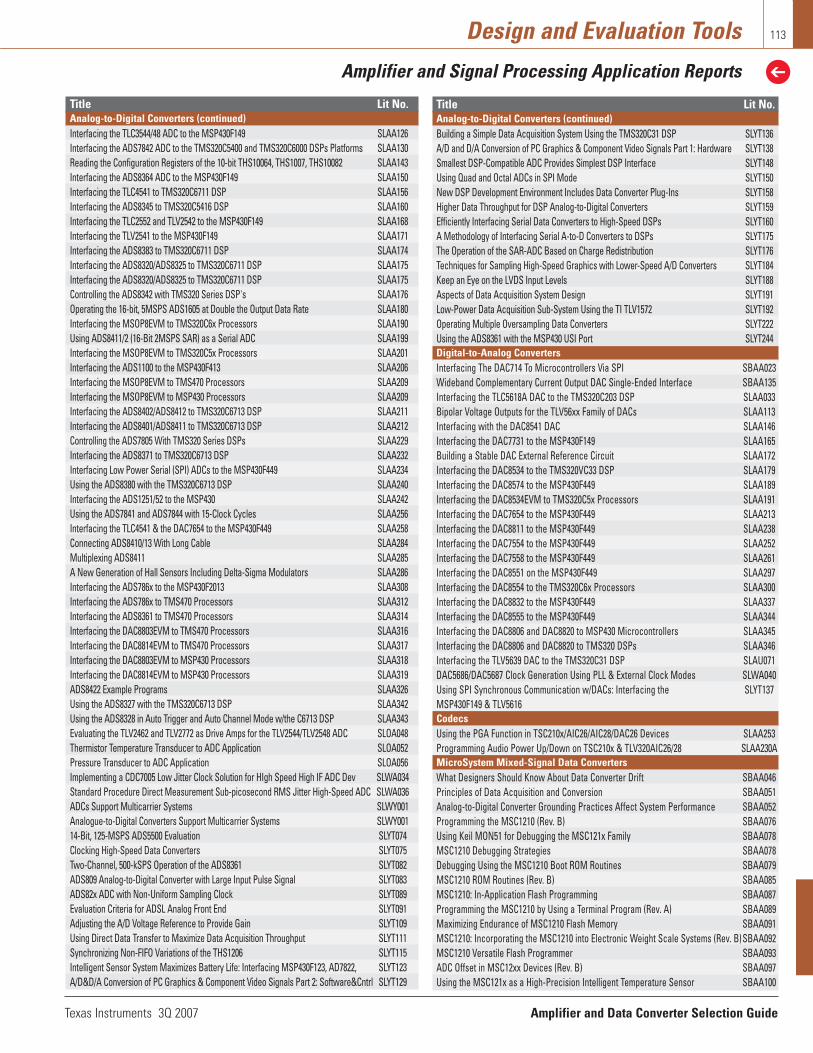
Texas Instruments 3Q 2007 Amplifier and Data Converter Selection Guide
Design and Evaluation Tools
Amplifier and Signal Processing Application Reports
113
Title Lit No.Analog-to-Digital Converters (continued)Interfacing the TLC3544/48 ADC to the MSP430F149 SLAA126Interfacing the ADS7842 ADC to the TMS320C5400 and TMS320C6000 DSPs Platforms SLAA130Reading the Configuration Registers of the 10-bit THS10064, THS1007, THS10082 SLAA143Interfacing the ADS8364 ADC to the MSP430F149 SLAA150Interfacing the TLC4541 to TMS320C6711 DSP SLAA156Interfacing the ADS8345 to TMS320C5416 DSP SLAA160Interfacing the TLC2552 and TLV2542 to the MSP430F149 SLAA168Interfacing the TLV2541 to the MSP430F149 SLAA171Interfacing the ADS8383 to TMS320C6711 DSP SLAA174Interfacing the ADS8320/ADS8325 to TMS320C6711 DSP SLAA175Interfacing the ADS8320/ADS8325 to TMS320C6711 DSP SLAA175Controlling the ADS8342 with TMS320 Series DSP's SLAA176Operating the 16-bit, 5MSPS ADS1605 at Double the Output Data Rate SLAA180Interfacing the MSOP8EVM to TMS320C6x Processors SLAA190Using ADS8411/2 (16-Bit 2MSPS SAR) as a Serial ADC SLAA199Interfacing the MSOP8EVM to TMS320C5x Processors SLAA201Interfacing the ADS1100 to the MSP430F413 SLAA206Interfacing the MSOP8EVM to TMS470 Processors SLAA209Interfacing the MSOP8EVM to MSP430 Processors SLAA209Interfacing the ADS8402/ADS8412 to TMS320C6713 DSP SLAA211Interfacing the ADS8401/ADS8411 to TMS320C6713 DSP SLAA212Controlling the ADS7805 With TMS320 Series DSPs SLAA229Interfacing the ADS8371 to TMS320C6713 DSP SLAA232Interfacing Low Power Serial (SPI) ADCs to the MSP430F449 SLAA234Using the ADS8380 with the TMS320C6713 DSP SLAA240Interfacing the ADS1251/52 to the MSP430 SLAA242Using the ADS7841 and ADS7844 with 15-Clock Cycles SLAA256Interfacing the TLC4541 & the DAC7654 to the MSP430F449 SLAA258Connecting ADS8410/13 With Long Cable SLAA284Multiplexing ADS8411 SLAA285A New Generation of Hall Sensors Including Delta-Sigma Modulators SLAA286Interfacing the ADS786x to the MSP430F2013 SLAA308Interfacing the ADS786x to TMS470 Processors SLAA312Interfacing the ADS8361 to TMS470 Processors SLAA314Interfacing the DAC8803EVM to TMS470 Processors SLAA316Interfacing the DAC8814EVM to TMS470 Processors SLAA317Interfacing the DAC8803EVM to MSP430 Processors SLAA318Interfacing the DAC8814EVM to MSP430 Processors SLAA319ADS8422 Example Programs SLAA326Using the ADS8327 with the TMS320C6713 DSP SLAA342Using the ADS8328 in Auto Trigger and Auto Channel Mode w/the C6713 DSP SLAA343Evaluating the TLV2462 and TLV2772 as Drive Amps for the TLV2544/TLV2548 ADC SLOA048Thermistor Temperature Transducer to ADC Application SLOA052Pressure Transducer to ADC Application SLOA056Implementing a CDC7005 Low Jitter Clock Solution for HIgh Speed High IF ADC Dev SLWA034Standard Procedure Direct Measurement Sub-picosecond RMS Jitter High-Speed ADC SLWA036ADCs Support Multicarrier Systems SLWY001Analogue-to-Digital Converters Support Multicarrier Systems SLWY00114-Bit, 125-MSPS ADS5500 Evaluation SLYT074Clocking High-Speed Data Converters SLYT075Two-Channel, 500-kSPS Operation of the ADS8361 SLYT082ADS809 Analog-to-Digital Converter with Large Input Pulse Signal SLYT083ADS82x ADC with Non-Uniform Sampling Clock SLYT089Evaluation Criteria for ADSL Analog Front End SLYT091Adjusting the A/D Voltage Reference to Provide Gain SLYT109Using Direct Data Transfer to Maximize Data Acquisition Throughput SLYT111Synchronizing Non-FIFO Variations of the THS1206 SLYT115Intelligent Sensor System Maximizes Battery Life: Interfacing MSP430F123, AD7822, SLYT123A/D&D/A Conversion of PC Graphics & Component Video Signals Part 2: Software&Cntrl SLYT129
Title Lit No.Analog-to-Digital Converters (continued)Building a Simple Data Acquisition System Using the TMS320C31 DSP SLYT136A/D and D/A Conversion of PC Graphics & Component Video Signals Part 1: Hardware SLYT138Smallest DSP-Compatible ADC Provides Simplest DSP Interface SLYT148Using Quad and Octal ADCs in SPI Mode SLYT150New DSP Development Environment Includes Data Converter Plug-Ins SLYT158Higher Data Throughput for DSP Analog-to-Digital Converters SLYT159Efficiently Interfacing Serial Data Converters to High-Speed DSPs SLYT160A Methodology of Interfacing Serial A-to-D Converters to DSPs SLYT175The Operation of the SAR-ADC Based on Charge Redistribution SLYT176Techniques for Sampling High-Speed Graphics with Lower-Speed A/D Converters SLYT184Keep an Eye on the LVDS Input Levels SLYT188Aspects of Data Acquisition System Design SLYT191Low-Power Data Acquisition Sub-System Using the TI TLV1572 SLYT192Operating Multiple Oversampling Data Converters SLYT222Using the ADS8361 with the MSP430 USI Port SLYT244Digital-to-Analog ConvertersInterfacing The DAC714 To Microcontrollers Via SPI SBAA023Wideband Complementary Current Output DAC Single-Ended Interface SBAA135Interfacing the TLC5618A DAC to the TMS320C203 DSP SLAA033Bipolar Voltage Outputs for the TLV56xx Family of DACs SLAA113Interfacing with the DAC8541 DAC SLAA146Interfacing the DAC7731 to the MSP430F149 SLAA165Building a Stable DAC External Reference Circuit SLAA172Interfacing the DAC8534 to the TMS320VC33 DSP SLAA179Interfacing the DAC8574 to the MSP430F449 SLAA189Interfacing the DAC8534EVM to TMS320C5x Processors SLAA191Interfacing the DAC7654 to the MSP430F449 SLAA213Interfacing the DAC8811 to the MSP430F449 SLAA238Interfacing the DAC7554 to the MSP430F449 SLAA252Interfacing the DAC7558 to the MSP430F449 SLAA261Interfacing the DAC8551 on the MSP430F449 SLAA297Interfacing the DAC8554 to the TMS320C6x Processors SLAA300Interfacing the DAC8832 to the MSP430F449 SLAA337Interfacing the DAC8555 to the MSP430F449 SLAA344Interfacing the DAC8806 and DAC8820 to MSP430 Microcontrollers SLAA345Interfacing the DAC8806 and DAC8820 to TMS320 DSPs SLAA346Interfacing the TLV5639 DAC to the TMS320C31 DSP SLAU071DAC5686/DAC5687 Clock Generation Using PLL & External Clock Modes SLWA040Using SPI Synchronous Communication w/DACs: Interfacing the SLYT137MSP430F149 & TLV5616CodecsUsing the PGA Function in TSC210x/AIC26/AIC28/DAC26 Devices SLAA253Programming Audio Power Up/Down on TSC210x & TLV320AIC26/28 SLAA230AMicroSystem Mixed-Signal Data ConvertersWhat Designers Should Know About Data Converter Drift SBAA046Principles of Data Acquisition and Conversion SBAA051Analog-to-Digital Converter Grounding Practices Affect System Performance SBAA052Programming the MSC1210 (Rev. B) SBAA076Using Keil MON51 for Debugging the MSC121x Family SBAA078MSC1210 Debugging Strategies SBAA078Debugging Using the MSC1210 Boot ROM Routines SBAA079MSC1210 ROM Routines (Rev. B) SBAA085MSC1210: In-Application Flash Programming SBAA087Programming the MSC1210 by Using a Terminal Program (Rev. A) SBAA089Maximizing Endurance of MSC1210 Flash Memory SBAA091MSC1210: Incorporating the MSC1210 into Electronic Weight Scale Systems (Rev. B)SBAA092MSC1210 Versatile Flash Programmer SBAA093ADC Offset in MSC12xx Devices (Rev. B) SBAA097Using the MSC121x as a High-Precision Intelligent Temperature Sensor SBAA100

Amplifier and Data Converter Selection Guide Texas Instruments 3Q 2007
Design and Evaluation Tools
Application Reports and Reference Designs
114
Title Lit No.MicroSystem Mixed-Signal Data Converters (continued)Getting Started with the MSC1210 SBAA102MSC12xx Programming with SDCC SBAA109Ratiometric Conversions: MSC1210, 1211, 1212 SBAA110Understanding the ADC Input on the MSC12xx SBAA111MSC1211 / 12 DAC INL Improvement SBAA112A Complete Webserver on the MSC121x SBAA114MSC12xx Serial Programming Board SBAA122Using Crystal Oscillators with MSC12xx MicroSystem Products SBAA123Average Measurements with the MSC12xx SBAA124Improving MSC120x Temperature Measurements SBAA126Incremental Flash Memory Page Erase SBAA137Minimizing Power Consumption on the MSC12xx SBAA139High-Speed Data Acquisition with MSC12xx Devices SBAA140Implementing IIR Filters on the MSC12xx SBAA142Supply Voltage Measurement and ADS PSRR Improvement in MSC12xx Devices SLYT073MSC1210 Debugging Strategies for High-Precision Smart Sensors SLYT110Touch Screen ControllersADS7843 Pen Interrupt SBAA028Touch Screen Controller Tips SBAA036Evaluating the ADS7846E: Using the DEM-ADS7843E/45E Evaluation Fixture SBAA037Using the ADS7846 Touch Screen Ctrl. with the Intel SA-1110 StrongArm Processor SBAA070Windows CE Touch and Keypad Device Drivers for the TSC2200 SBAA075Applying the Current DAC on the TSC2000, TSC2200, TSC2300, and TSC2301 Touch Screen SBAA098Windows CE .NET Touch Screen, Keypad and Audio Device Drivers for the TSC2301 SLAA169TCS2301 WinCE Generic Drivers SLAA187Programming Sequences and Tips for TSC2000/2200/230x Applications SLAA197TSC2100 WinCE Generic Drivers SLAA198TSC2101 Touch Screen, Battery and Audio WinCE Drivers SLAA200Interface TSC Through McBSP SLAA214
Title Lit No.Touch Screen Controllers (continued)TSC2101 WinCE 5.0 Drivers SLAA251TSC2003 WinCE 5.0 Driver SLAA277TSC2046 WinCE 5.0 Driver SLAA278TSC2100 WinCE5.0 Drivers SLAA292How to Use TI's 4-Wire TSC to Control an 8-Wire Resistive Touch Screen SLAA298Apply TI TSC for Various and Multiple Functions SLAA339Voiceband Codecs (continued)0Designing with the TLC320AC01 Analog Interface for DSPs SLAA006Common Sample Rate Selection For TLV320AIC12/13/14/15/20/21/24/25 Codecs SLAA009Multiple TLC320AC01/02 Analog I/F Circuits on One TMS320C5x DSP Serial Port SLAA016Evaluation Board for the TLC320AD545 DSP Analog Interface Circuit (Rev. A) SLAA085aDesign Guidelines for the TLC320AD50 SLAA087Comparison of TI Voiceband Codecs for Telephony Applications SLAA088Design Guidelines for the TLC320AD535/545 SLAA090Interfacing the TMS320C54x DSP to the TLC320AD535/545 Codecs SLAA091Interfacing the TLV320AIC10/11 Codec to the TMS320C5402 DSP SLAA109TLV320AIC12/13/14/15 CODEC Operating Under Stand-Alone Slave Mode SLAA142Sample Code for Interfacing the TLV320AIC1106 CODEC with the TMS320C5402 DSP SLAA147Demo/Test CODEC System with TLV320AIC20/21/24/25 EVM SLAA153Interfacing the TLV320AIC12/13/14/15 Codec to the TMS320C5402y DSP SLAA154Interface the TLV320AIC1110 CODEC With The TMS320C5402 DSP SLAA158TMS320C54x DSP Reference Framework & Device Driver for the TLV320AIC20 HPA DC SLAA166Interface with Voice-Band Codecs Using I2C SLAA173Efficient Resampling Filters for the AIC111 SLAA193Hardware auto-identification&software auto-configuration for the SLYT149aTLV320AIC10 DSP Codec - a "plug-and-play" algorithmInterfacing Two Analog Interface Circuits to One TMS320C5x Serial Port SPRA268TMS320C54xx McBSP to TLV320AIC24 Interface SPRA957
ADS1230/ADS1232REF: Weigh Scale Reference DesignBuilt around an ultra-low-powerMSP430F449, this fully functional weighscale board (just add your own load cell) canbe used by itself, powered from a 9V battery.The LCD display and simple push buttons pro-vide an easy-to-use interface that allows youto calibrate the scale, adjust for tare, andmake measurements in several different unitsof weight (grams, ounces, pounds, etc). AUSB interface allows the board to connect to
ADS8410/13REF: High-Speed SAR withLVDS Interface Reference DesignThe ADS8410/ADS8413REF, designed by AvnetDesign Services, allows the high-speed analogsystems designer a fully functional referenceplatform to evaluate the TI ADS841x family of16-bit SAR, 2MSPS analog-to-digital converters.The analog front-end design allows raw signalsto be fed into either a differential or singleended topology while the Xilinx® Spartan™-3FPGA allows the system the flexibility of independent or cascaded LVDS modes. The signal is displayed on a LabVIEW™ console via a USB link to the PC.
Reference Designs
ADS8410/13REF:• Two-channel data acquisition system
based on the ADS841x, 16-bit, 2MSPS ADC• Single-ended or differential analog input
stage configuration• Front-end signal conditioning included• Outputs can be cascaded to support
daisy chaining• Xilinx Spartan-3 FPGA• LVDS data path from ADCs• USB 2.0 interface to PC• 16 MB SDRAM• Controlled via host PC
a PC and the data collected can be viewedand analyzed with the included software. Allsource code for the firmware and software,as well as the PCB design files, are availableby contacting TI.
ADS1230/ADS1232REF:• Fully functional weigh scale• MSP430-based• Operates alone or connected to a PC• Firmware and software source code and
Gerber files available

Texas Instruments 3Q 2007 Amplifier and Data Converter Selection Guide
Device Index 115
Device PageACF2101 ............................ 48ADS1000 ...................... 55, 92ADS1100 .............. 55, 88, 112ADS1110........................55, 88ADS1112 ...................... 55, 88ADS1201 .............. 79, 86, 112ADS1202 .. 77, 79, 80, 88, 112ADS1203 .......... 77, 79, 80, 88ADS1204 .......... 77, 79, 80, 88ADS1205 .......... 77, 79, 80, 88ADS1208 .......... 77, 79, 80, 88ADS1210 .............. 55, 86, 112ADS1211 .................... 86, 112ADS1212 .............. 55, 86, 112ADS1213 .................... 86, 112ADS1216 ...... 55, 86, 107, 112ADS1217 ...... 55, 86, 107, 112ADS1218 ...... 55, 86, 107, 112ADS1222 ...................... 55, 86ADS1224 ...................... 55, 86ADS1225 ................ 54, 55, 86ADS1226 ................ 54, 55, 86ADS1230 ........ 53, 55, 87, 114ADS1232 ................ 53, 55, 86ADS1234 ................ 53, 55, 86ADS1240 ...... 55, 86, 107, 112ADS1241 ...... 55, 86, 107, 112ADS1242 ...................... 55, 86ADS1243 ...................... 55, 86ADS1244 .............. 55, 86, 112ADS1245 .............. 55, 86, 112ADS1250 ...................... 55, 86ADS1251 ...... 55, 86, 107, 112ADS1252 ...... 55, 86, 107, 112ADS1253 ...... 55, 86, 107, 112ADS1254 ...... 55, 86, 107, 112ADS1255 .............. 55, 86, 112ADS1256 ...................... 55, 86ADS1258 ........ 53, 55, 86, 107ADS1271 54, 55, 86, 107, 112ADS1274 ................ 54, 55, 86ADS1278 ................ 54, 55, 86ADS1286 ...................... 63, 92ADS1601 .............. 56, 87, 107ADS1602 .............. 56, 87, 107ADS1605 ...... 56, 87, 107, 112ADS1606 .............. 56, 87, 107ADS1610 .............. 56, 87, 107ADS1625 .............. 56, 87, 107ADS1626 .............. 56, 87, 107ADS2806 ...................... 68, 90ADS2807 ...................... 67, 90ADS5102 ...................... 68, 92ADS5103 ...................... 68, 92ADS5120 ...................... 68, 92ADS5121 ...................... 68, 92ADS5122 ...................... 68, 92ADS5203 ...................... 68, 92ADS5204 ...................... 68, 92ADS5220 ...................... 67, 90
Device PageADS5221 ...................... 67, 90ADS5231 ...................... 67, 90ADS5232 ...................... 67, 90ADS5240 ...................... 68, 90ADS5242 ...................... 67, 90ADS5270 ...................... 68, 90ADS5271 ...................... 67, 90ADS5272 ...................... 67, 90ADS5273 ...................... 67, 90ADS5277 ...................... 68, 92ADS5410 ...................... 67, 90ADS5411 ...................... 68, 92ADS5413 ...................... 67, 90ADS5413-11 ................ 68, 92ADS5421 ...................... 67, 89ADS5422 ...................... 67, 89ADS5423 ................ 65, 67, 89ADS5424 ........ 65, 67, 89, 111ADS5433 ................ 65, 67, 89ADS5440 ................ 66, 67, 89ADS5444 ................ 66, 67, 89ADS5463 ................ 66, 67, 89ADS5500 ...... 67, 88, 112, 113ADS5500-EP ...................... 88ADS5510 ...................... 68, 92ADS5520 ...................... 67, 89ADS5521 ...................... 67, 90ADS5522 ...................... 67, 90ADS5525 ................ 66, 67, 89ADS5527 ................ 66, 67, 89ADS5541 ...................... 67, 88ADS5542 ...................... 67, 89ADS5545 .......... 66, 67, 88, 89ADS5546 .......... 66, 67, 88, 89ADS5547 ................ 66, 67, 88ADS5553 ...................... 67, 89ADS6223 ...................... 67, 90ADS6224 ...................... 67, 90ADS6225 ...................... 67, 89ADS6243 ...................... 67, 89ADS6244 ...................... 67, 89ADS6245 ...................... 67, 88ADS6423 ...................... 67, 90ADS6424 ...................... 67, 90ADS6425 ................ 65, 67, 89ADS6443 ...................... 67, 89ADS6444 ...................... 67, 89ADS6445 ................ 65, 67, 88ADS7800 .............. 62, 91, 112ADS7804 .............. 62, 91, 107ADS7805 ...... 62, 88, 107, 112ADS7806 ...................... 62, 92ADS7807 ...................... 62, 88ADS7808 ...................... 62, 91ADS7809 .............. 62, 88, 112ADS7810 ................ 61, 62, 90ADS7811 ...................... 62, 88ADS7812 ...................... 62, 92ADS7813 ...................... 62, 88
Device PageADS7815 ...................... 62, 88ADS7816 ...................... 63, 91ADS7817 .............. 63, 91, 112ADS7818 ...................... 61, 91ADS7822 .............. 63, 91, 112ADS7823 ...................... 63, 92ADS7824 .............. 62, 92, 112ADS7825 .............. 62, 88, 112ADS7826 ...................... 63, 93ADS7827 ...................... 63, 93ADS7828 ...................... 63, 91ADS7829 .............. 63, 91, 107ADS7830 ...................... 63, 93ADS7834 ...................... 61, 91ADS7835 ................ 61, 62, 91ADS7841 ...... 63, 91, 107, 113ADS7842 .............. 63, 91, 112ADS7843 .................. 100, 113ADS7844 .............. 62, 91, 113ADS7845 .......................... 100ADS7846 .................. 100, 113ADS7852 ...................... 61, 91ADS7861 ........ 61, 79, 91, 107ADS7862 ........ 61, 79, 91, 112ADS7863 ................ 61, 79, 90ADS7864 ........ 61, 79, 91, 107ADS7866 ...................... 63, 91ADS7867 ...................... 63, 93ADS7868 ...................... 63, 93ADS7869 .. 61, 77, 79, 90, 112ADS7870 ........ 63, 79, 91, 112ADS7871 ................ 62, 79, 89ADS7881 .............. 61, 90, 108ADS7886 ...................... 61, 90ADS7887 ...................... 61, 92ADS7888 ...................... 61, 93ADS7890 ...................... 61, 89ADS7891 .............. 61, 89, 108ADS800 ........................ 67, 90ADS801 ........................ 68, 90ADS802 ........................ 68, 90ADS803 ................ 68, 90, 108ADS804 ................ 68, 90, 108ADS805 ................ 68, 90, 108ADS807 ........................ 67, 90ADS808 ........................ 67, 90ADS809 ................ 67, 90, 113ADS820 ........................ 68, 92ADS821 ........................ 68, 92ADS822 ........................ 68, 92ADS822/825 ...................... 92ADS823 .............................. 68ADS825 .............................. 68ADS826 ........................ 68, 92ADS826/823 ...................... 92ADS828 ........................ 68, 92ADS830 ........................ 68, 93ADS831 ........................ 68, 93ADS8317 ...................... 62, 88
Device PageADS8320 ...... 62, 88, 108, 112ADS8321 .............. 62, 88, 108ADS8322 .............. 61, 87, 108ADS8323 .............. 61, 87, 108ADS8324 ........ 62, 81, 89, 108ADS8325 ...... 62, 88, 108, 112ADS8326 ...................... 62, 88ADS8327 ........ 60, 61, 87, 113ADS8328 ........ 60, 61, 87, 113ADS8329 ................ 60, 61, 87ADS8330 ................ 60, 61, 87ADS8341 ...................... 62, 88ADS8342 ...... 62, 87, 111, 112ADS8343 ...................... 62, 88ADS8344 ...................... 62, 88ADS8345 .............. 62, 88, 112ADS8361 .......... 27, 61, 79, 87
108, 112, 113ADS8364 .......... 62, 78, 79, 87
108, 112ADS8365 .......... 62, 78, 79, 87ADS8370 .............. 61, 87, 108ADS8371 ...... 61, 87, 108, 112ADS8372 .............. 61, 87, 108ADS8380 ...... 61, 87, 108, 112ADS8381 .............. 61, 87, 108ADS8382 .............. 61, 87, 108ADS8383 ...... 61, 87, 108, 112ADS8401 ...... 61, 87, 108, 112ADS8402 ...... 61, 87, 108, 112ADS8405 .............. 61, 87, 108ADS8406 .............. 61, 87, 108ADS8410 .............. 61, 87, 111
113, 114ADS8411 .............. 61, 87, 108
111-113ADS8412 ...... 61, 87, 108, 112ADS8413 ...................... 61, 87ADS8422 59, 61, 87, 108, 113ADS8472 ................ 60, 61, 87ADS8481 ........ 60, 61, 87, 108ADS8482 ........ 60, 61, 87, 108ADS8484 ...................... 61, 87ADS850 ........................ 67, 89ADS8504 ........ 59, 62, 91, 108ADS8505 .. 11, 59, 62, 88, 108ADS8506 ................ 59, 62, 91ADS8507 ................ 59, 62, 88ADS8508 ................ 59, 62, 91ADS8509 ................ 59, 62, 88ADS8513 ................ 59, 62, 88ADS8515 ...................... 61, 88ADS900 ........................ 68, 92ADS901 ........................ 68, 92ADS930 ........................ 68, 93ADS931 ........................ 68, 93AIC111 .............. 100, 110, 114AMC1210................ 77, 79, 80AMC6821...................... 78, 84
Device PageAMC7820 ...... 63, 79, 91, 110AMC7823 62, 77, 79, 91, 110BUF602 ...... 15, 18, 20, 22, 43BUF634 .... 15, 18, 42, 43, 111DAC1220 .............. 69, 94, 109DAC1221 .............. 69, 95, 109DAC2900 ...................... 76, 97DAC2902 ...................... 76, 95DAC2904 ...................... 76, 95DAC2932 ...................... 76, 95DAC5571 ...................... 74, 97DAC5573 ...................... 74, 97DAC5574 ...................... 74, 97DAC5652 ...................... 76, 97DAC5652-EP ...................... 97DAC5662 ...................... 76, 95DAC5662-EP ...................... 95DAC5672 ...................... 76, 95DAC5672-EP ...................... 95DAC5674 ...................... 76, 95DAC5675 ...................... 76, 95DAC5675-EP ...................... 95DAC5686 .............. 76, 94, 113DAC5687 .............. 76, 94, 113DAC5687-EP ...................... 94DAC6571 ...................... 74, 97DAC6573 ...................... 74, 97DAC6574 ...................... 74, 97DAC712 ........................ 72, 94DAC714 ................ 72, 94, 113DAC715 ........................ 73, 94DAC716 ........................ 73, 94DAC7512 .............. 74, 96, 109DAC7513 .............. 74, 96, 109DAC7541 ...................... 72, 96DAC7545 ...................... 73, 96DAC7551 .............. 74, 96, 109DAC7552 .............. 74, 96, 109DAC7553 ...................... 74, 96DAC7554 ...... 74, 96, 109, 113DAC7558 .............. 74, 96, 113DAC7571 ...................... 74, 97DAC7573 ...................... 74, 96DAC7574 ...................... 74, 96DAC7611 ...................... 74, 97DAC7612 ...................... 74, 96DAC7613 ...................... 73, 97DAC7614 ...................... 73, 96DAC7615 ...................... 73, 96DAC7616 ...................... 73, 96DAC7617 ...................... 73, 96DAC7621 ...................... 74, 97DAC7624 ...................... 73, 96DAC7625 ...................... 73, 96DAC7631 ...................... 72, 95DAC7632 ...................... 72, 94DAC7634 ...................... 72, 94DAC7641 ...................... 72, 95DAC7642 ...................... 72, 94
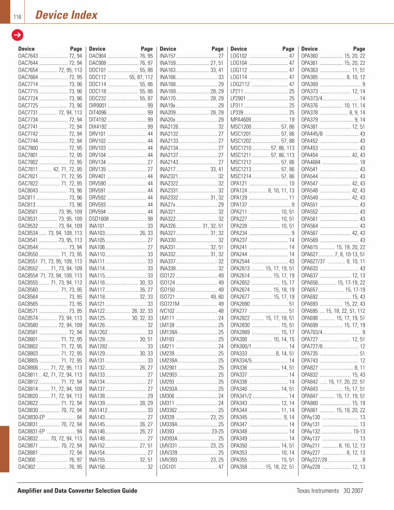
Amplifier and Data Converter Selection Guide Texas Instruments 3Q 2007
Device Index116
Device PageDAC7643 ...................... 72, 94DAC7644 ...................... 72, 94DAC7654 .............. 72, 95, 113DAC7664 ...................... 72, 95DAC7714 ...................... 73, 96DAC7715 ...................... 73, 96DAC7724 ...................... 73, 96DAC7725 ...................... 73, 96DAC7731 .............. 72, 94, 113DAC7734 ...................... 72, 94DAC7741 ...................... 72, 94DAC7742 ...................... 72, 94DAC7744 ...................... 72, 94DAC7800 ...................... 72, 95DAC7801 ...................... 72, 95DAC7802 ...................... 72, 95DAC7811 .......... 42, 71, 72, 95DAC7821 ................ 71, 72, 95DAC7822 ................ 71, 72, 95DAC8043 ...................... 73, 96DAC811 ........................ 73, 96DAC813 ........................ 73, 96DAC8501 .............. 73, 95, 109DAC8531 .............. 73, 95, 109DAC8532 .............. 73, 94, 109DAC8534 ...... 73, 94, 109, 113DAC8541 .............. 73, 95, 113DAC8544 ...................... 73, 94DAC8550 ................ 71, 73, 95DAC8551 71, 73, 95, 109, 113DAC8552 ........ 71, 73, 94, 109DAC8554 71, 73, 94, 109, 113DAC8555 ........ 71, 73, 94, 113DAC8560 ................ 71, 73, 95DAC8564 ...................... 73, 95DAC8565 ...................... 73, 95DAC8571 ...................... 73, 95DAC8574 .............. 73, 94, 113DAC8580 .............. 72, 94, 109DAC8581 ...................... 72, 94DAC8801 ................ 71, 72, 95DAC8802 ................ 71, 72, 95DAC8803 ................ 71, 72, 95DAC8805 ................ 71, 72, 95DAC8806 ........ 71, 72, 95, 113DAC8811 .. 42, 71, 72, 94, 113DAC8812 ................ 71, 72, 94DAC8814 ........ 71, 72, 94, 109DAC8820 ........ 71, 72, 94, 113DAC8822 ................ 71, 72, 94DAC8830 ................ 70, 72, 94DAC8830-EP ...................... 94DAC8831 ................ 70, 72, 94DAC8831-EP ...................... 94DAC8832 ........ 70, 72, 94, 113DAC8871 ................ 70, 72, 94DAC8881 ...................... 72, 94DAC900 ........................ 76, 97DAC902 ........................ 76, 95
Device PageDAC904 ........................ 76, 95DAC908 ........................ 76, 97DDC101 ........................ 55, 86DDC112 ................ 55, 87, 112DDC114 ........................ 55, 86DDC118 ........................ 55, 86DDC232 ........................ 55, 87DIR9001 .............................. 99DIT4096 .............................. 99DIT4192 .............................. 99DIX4192 .............................. 99DRV101 .............................. 44DRV102 .............................. 44DRV103 .............................. 44DRV104 .............................. 44DRV134 .............................. 27DRV135 .............................. 27DRV401 .............................. 44DRV590 .............................. 44DRV591 .............................. 44DRV592 .............................. 44DRV593 .............................. 44DRV594 .............................. 44DSD1608 ............................ 98INA101................................ 33INA103.......................... 26, 33INA105................................ 27INA106................................ 27INA110................................ 33INA111................................ 33INA114................................ 33INA115................................ 33INA116.......................... 30, 33INA117.......................... 26, 27INA118.......................... 32, 33INA121................................ 33INA122.................... 26, 32, 33INA125.................... 30, 32, 33INA126................................ 32INA1262.............................. 33INA128.......................... 30, 51INA1282.............................. 33INA129.......................... 30, 33INA131................................ 33INA132.......................... 26, 27INA133................................ 27INA134................................ 27INA137................................ 27INA138................................ 29INA139.......................... 28, 29INA1412.............................. 33INA143................................ 27INA145.......................... 26, 27INA146.......................... 26, 27INA148................................ 27INA152.......................... 27, 51INA154................................ 27INA155.......................... 32, 51INA156................................ 32
Device PageINA157................................ 27INA159.......................... 27, 51INA163.......................... 33, 41INA166................................ 33INA168................................ 29INA169.......................... 28, 29INA170.......................... 28, 29INA19x ................................ 29INA209.......................... 28, 29INA20x ................................ 29INA2126.............................. 32INA2132.............................. 27INA2133.............................. 27INA2134.............................. 27INA2137.............................. 27INA2143.............................. 27INA217.......................... 33, 41INA2321.............................. 32INA2322.............................. 32INA2331.............................. 32INA2332........................ 31, 32INA27x ................................ 29INA321................................ 32INA322................................ 32INA326.................... 31, 32, 51INA327.......................... 31, 32INA330................................ 32INA331.......................... 32, 51INA332.......................... 31, 32INA337................................ 32INA338................................ 32ISO122 ................................ 49ISO124 ................................ 49ISO150 ................................ 49ISO721 .......................... 49, 80ISO721M ............................ 49IVC102 ................................ 48LM111 ................................ 24LM139 ................................ 25LM139A .............................. 25LM193 ................................ 25LM211 ................................ 24LM239 ................................ 25LM239A .............................. 25LM2901 .............................. 25LM2903 .............................. 25LM293 ................................ 25LM293A .............................. 25LM306 ................................ 24LM311 ................................ 24LM3302 .............................. 25LM339 .......................... 23, 25LM339A .............................. 25LM393 .......................... 23-25LM393A .............................. 25LMV331 ........................ 23, 25LMV339 .............................. 25LMV393 ........................ 23, 25LOG101 .............................. 47
Device PageLOG102 .............................. 47LOG104 .............................. 47LOG112 .............................. 47LOG114 .............................. 47LOG2112 ............................ 47LP211 .................................. 25LP2901 ................................ 25LP311 .................................. 25LP339 .................................. 25MPA4609 ............................ 19MSC1200...................... 57, 86MSC1201...................... 57, 86MSC1202...................... 57, 88MSC1210.............. 57, 86, 113MSC1211.............. 57, 86, 113MSC1212...................... 57, 86MSC1213...................... 57, 86MSC1214...................... 57, 86OPA121 .............................. 10OPA124 .............. 8, 10, 11, 13OPA129 .............................. 11OPA137 ................................ 9OPA211 ........................ 10, 51OPA227 ........................ 10, 51OPA228 ........................ 10, 51OPA234 ................................ 9OPA237 .............................. 14OPA241 .............................. 14OPA244 .............................. 14OPA2544 ............................ 43OPA2613 .......... 15, 17, 19, 51OPA2614 ................ 15, 17, 19OPA2652 ...................... 15, 17OPA2674 ................ 15, 18, 19OPA2677 ................ 15, 17, 19OPA2690 ............................ 51OPA277 .............................. 51OPA2822 .......... 15, 17, 18, 51OPA2830 ...................... 15, 51OPA2889 ...................... 15, 17OPA300 .................. 10, 14, 15OPA300/1............................ 14OPA333 .................... 8, 14, 51OPA334/5............................ 14OPA336 ........................ 14, 51OPA337 .............................. 14OPA338 .............................. 14OPA340 ........................ 14, 51OPA341/2............................ 14OPA343 ........................ 12, 14OPA344 ........................ 11, 14OPA345 .......................... 9, 14OPA347 .............................. 14OPA348 .............................. 14OPA349 .............................. 14OPA350 ........................ 14, 51OPA353 ........................ 10, 14OPA355 ........................ 15, 51OPA358 ............ 15, 18, 22, 51
Device PageOPA360 .................. 15, 20, 22OPA361 .................. 15, 20, 22OPA363 ........................ 11, 51OPA365 .................... 8, 10, 12OPA369 ................................ 9OPA373 ........................ 12, 14OPA373/4............................ 14OPA376 .................. 10, 11, 14OPA378 ...................... 8, 9, 14OPA379 .......................... 9, 14OPA381 ........................ 12, 51OPA445/B .......................... 43OPA452 .............................. 43OPA453 .............................. 43OPA454 ........................ 42, 43OPA4684 ............................ 18OPA541 .............................. 43OPA544 .............................. 43OPA547 ........................ 42, 43OPA548 ........................ 42, 43OPA549 ........................ 42, 43OPA551 .............................. 43OPA552 .............................. 43OPA561 .............................. 43OPA564 .............................. 43OPA567 ........................ 42, 43OPA569 .............................. 43OPA615 ............ 15, 19, 20, 22OPA627............ 7, 8, 10-13, 51OPA627/37 .............. 8, 10, 11OPA633 .............................. 43OPA637 ........................ 12, 13OPA656.............. 15, 17-19, 22OPA657.................... 15, 17-19OPA692 ........................ 15, 43OPA693 .................. 15, 22, 43OPA695 .... 15, 18, 22, 51, 112OPA698 ............ 15, 17, 19, 51OPA699 .................. 15, 17, 19OPA703/4.............................. 9OPA727 ........................ 12, 51OPA727/8............................ 12OPA735 .............................. 51OPA743 .............................. 12OPA827 .......................... 8, 11OPA832 ........................ 15, 43OPA842 ...... 15, 17, 20, 22, 51OPA843 .................. 15, 17, 51OPA847 ............ 15, 17, 19, 51OPA860 ........................ 15, 19OPA861 ............ 15, 19, 20, 22OPAy130 ............................ 13OPAy131 ............................ 13OPAy132 ........................ 10-13OPAy137 ............................ 13OPAy211 ............ 8, 10, 12, 13OPAy227 .................. 8, 12, 13OPAy227/28 .......................... 8OPAy228 ...................... 12, 13
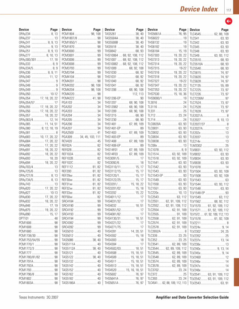
Texas Instruments 3Q 2007 Amplifier and Data Converter Selection Guide
Device Index 117
Device PageOPAy234 ........................ 8, 13OPAy237 ............................ 13OPAy241 .................... 8, 9, 13OPAy244 ........................ 9, 13OPAy251 .................... 8, 9, 13OPAy277 .................. 8, 10, 13OPAy300/301................ 17, 18OPAy333 .......................... 8, 9OPAy334/5........................ 8, 9OPAy336 .................... 8, 9, 11OPAy340 ...................... 11, 12OPAy347 .............................. 9OPAy348 .............................. 9OPAy349 .............................. 9OPAy350 ........................ 10-12OPAy354 .......... 17, 18, 20, 22OPAy354/57 ........................ 17OPAy355 .......... 17, 18, 20, 22OPAy356 .......... 17, 18, 20, 22OPAy357 ................ 18, 20, 22OPAy363/4.................... 12, 14OPAy365 ................ 11, 14, 51OPAy380 ............ 8, 12, 18, 19OPAy381 .............................. 8OPAy683 .......... 10, 17, 20, 22OPAy684 ................ 17, 20, 22OPAy690 ................ 17, 20, 22OPAy691 ................ 18, 20, 22OPAy692 ................ 18, 20, 22OPAy693 ...................... 18, 20OPAy694 ................ 18, 20, 22OPAy703/4 .......................... 13OPAy725/6 .......................... 13OPAy727/8...................... 8, 13OPAy734/5...................... 8, 13OPAy743 ............................ 13OPAy820 ................ 17, 20, 22OPAy827 ........................ 10-13OPAy830 ................ 17, 20, 22OPAy832 ................ 18, 20, 22OPAy846 ...................... 17, 19OPAy875 ................ 19, 20, 22OPAy890 ...................... 15, 17OPT101 .............................. 48PCM1606 ............................ 98PCM1608 ............................ 98PCM1680 ............................ 98PCM1738/30 ...................... 98PCM1753/54/55 ................ 98PCM1770/1 ........................ 98PCM1772/3 ........................ 98PCM1777 ............................ 98PCM1780/81/82 ................ 98PCM1791A.......................... 98PCM1792A.......................... 98PCM1793 ............................ 98PCM1796/8 ........................ 98PCM1802 ............................ 98PCM1803A.......................... 98
Device PagePCM1804 .................... 98, 108PCM1807/8 ........................ 98PCM1850/1 ........................ 98PCM1870 ............................ 98PCM3000 ............................ 99PCM3001 ............................ 99PCM3006 ............................ 99PCM3008 ............................ 99PCM3793 ............................ 99PCM3794 ............................ 99PCM4104 ............................ 98PCM4201 ............................ 98PCM4202 .................... 98, 108PCM4204 .................... 98, 108PCM4220 ............................ 98PCM4222 ...................... 41, 98PGA103 .............................. 34PGA202 .............................. 34PGA203 .............................. 34PGA204 .............................. 34PGA205 .............................. 34PGA206 .............................. 34PGA207 .............................. 34PGA2500 ............................ 41PGA309 ........ 34, 45, 103, 111RCV420 .............................. 45REF02A .............................. 82REF02B................................ 82REF102A ............................ 82REF102B.............................. 82REF102C.............................. 82REF1112........................ 81, 82REF200.......................... 81, 82REF29xx ........................ 81, 82REF30xx ........................ 81, 82REF31xx ........................ 81, 82REF32xx ........................ 81, 82REF33xx ........................ 81, 82REF50xx .............................. 82SRC4184 ............................ 99SRC4190 ............................ 99SRC4192 ............................ 99SRC4193 ............................ 99SRC4194 ............................ 99SRC4382 ............................ 99SRC4392 ............................ 99TAS5010 ............................ 40TAS5012 ............................ 40TAS5086 ...................... 38, 40TAS5111A .......................... 40TAS5112A .................... 38, 40TAS5121 ............................ 40TAS5122 ...................... 38, 40TAS5132 ............................ 40TAS5142 ............................ 40TAS5152 ............................ 40TAS5162 ............................ 40TAS5182 ............................ 40TAS5186A .......................... 40
Device PageTAS5261 ...................... 38, 40TAS5504A .................... 38, 40TAS5508B .................... 38, 40TAS5518 ...................... 38, 40THS0842 ...................... 68, 93THS10064 .... 68, 92, 108, 112THS1007 ...... 68, 92, 108, 112THS10082 .... 68, 92, 108, 112THS1009 .............. 68, 92, 108THS1030 ...................... 68, 92THS1031 ...................... 68, 92THS1040 ...................... 68, 92THS1041 ...................... 68, 92THS1206 .............. 68, 90, 108
112, 113THS1206-EP ........................ 90THS1207 .............. 68, 90, 108THS12082 ............ 68, 90, 108THS1209 .............. 68, 90, 108THS1215 ...................... 68, 90THS1230 ...................... 68, 90THS1401 .............. 67, 89, 109THS1401-EP ........................ 89THS1403 .............. 67, 89, 109THS1403-EP ........................ 89THS1408 .............. 67, 89, 109THS1408-EP ........................ 89THS14F01 ............ 67, 89, 109THS14F03 ............ 67, 89, 109THS3091/5.......................... 17THS3092/6.......................... 18THS3110/11.................. 15, 17THS3112/15.................. 15, 17THS3120/1.................... 15, 17THS3122/25.................. 15, 17THS3201/................ 15, 18, 22THS3201/02.................. 15, 18THS3202 ...................... 15, 22THS4011/12........................ 17THS4031/32........................ 17THS4032 ...................... 18, 51THS4051/52........................ 17THS4081/82........................ 17THS4130/31.................. 18, 51THS4221/22........................ 17THS4271/75........................ 17THS4281 ................ 14, 20, 51THS4302 ...................... 15, 18THS4303 ............................ 18THS4304 ............................ 17THS4502/03.................. 18, 51THS4508 ................ 15, 18, 51THS4509 ................ 15, 18, 51THS4511 ................ 15, 18, 51THS4513 ................ 15, 18, 51THS4520 .......... 15, 16, 18, 51THS5602 ...................... 76, 97THS5641A .................... 76, 97THS5651A .................... 76, 97
Device PageTHS5661A .................... 76, 95THS6022 ............................ 19THS6132 ............................ 19THS6182 ............................ 19THS6184 ...................... 15, 19THS7303 ................ 19, 20, 22THS7313 ................ 19, 20, 22THS7314 ................ 19, 20, 22THS7315 ........................ 19-22THS7316 ................ 19, 20, 22THS7318 ................ 19, 20, 22THS7327 ........................ 19-22THS7347 ................ 19, 20, 22THS7353 ................ 19, 20, 22THS7530 ................ 15, 18, 36THS9000/1.......................... 19TL3016 ................................ 24TL3116 ................................ 24TL331 .................................. 25TL712 ............................ 23, 24TL714 .................................. 24TLC0820A .................... 63, 93TLC0831........................ 63, 93TLC0832........................ 63, 93TLC0834........................ 63, 93TLC0838........................ 63, 93TLC08x ................................ 13TLC1078............................ 8, 9TLC1514................ 63, 92, 109TLC1518................ 63, 92, 109TLC1541........................ 63, 93TLC1542........................ 63, 93TLC1543........................ 63, 93TLC1543-EP ........................ 93TLC1549........................ 63, 93TLC1550........................ 63, 93TLC1551........................ 63, 93TLC220x ........................ 10, 13TLC2543...................... 63, 112TLC2551........ 62, 91, 109, 112TLC2552........ 62, 91, 109, 112TLC2554................ 62, 91, 109TLC2555...................... 91, 109TLC2558................ 62, 91, 109TLC2574................ 62, 91, 109TLC2578................ 62, 91, 109TLC2652A ............................ 8TLC339.......................... 23, 25TLC352.......................... 23, 25TLC3541................ 62, 89, 109TLC3544........ 62, 89, 109, 112TLC3545................ 62, 89, 109TLC3548................ 62, 89, 109TLC3574................ 62, 89, 109TLC3578................ 62, 89, 109TLC3702........................ 23, 24TLC372 ................................ 25TLC393.......................... 23, 24TLC4541...... 62, 88, 109, 112, 113
Device PageTLC4545................ 62, 88, 109TLC541.......................... 63, 93TLC542.......................... 63, 93TLC545.......................... 63, 93TLC548.......................... 63, 93TLC549.................. 63, 93, 112TLC5510........................ 68, 93TLC5510A .................... 68, 93TLC5540........................ 68, 93TLC5615........................ 74, 97TLC5620........................ 74, 97TLC5628........................ 74, 97TLC7135........................ 55, 89TLC7225........................ 73, 97TLC7226........................ 73, 97TLC7226M .......................... 97TLC7524........................ 73, 97TLC7528........................ 73, 97TLC7628........................ 73, 97TLE2021A.............................. 8TLE2027 .................... 8, 10, 13TLE2027/37 .......................... 8TLE2027A............................ 12TLE202x .............................. 13TLE2037 .............................. 13TLE214x .............................. 13TLM3302 ............................ 25TLV0831 ................ 63, 93, 112TLV0832 ........................ 63, 93TLV0834 ........................ 63, 93TLV0838 ........................ 63, 93TLV1078 .............................. 14TLV1504 ................ 63, 93, 109TLV1508 ................ 63, 92, 109TLV1543 .............................. 63TLV1544 ................ 63, 93, 112TLV1548 ........................ 63, 93TLV1548-EP ........................ 93TLV1549 ...................... 63, 112TLV1562 ................ 68, 92, 112TLV1570........ 61, 92, 109, 112TLV1571........ 61, 92, 109, 112TLV1572...... 61, 92, 109, 112, 113TLV1578 ................ 61, 92, 109TLV2211 ................................ 8TLV224x .......................... 9, 14TLV2302 ........................ 24, 25TLV2352 .............................. 25TLV237x ........................ 13, 14TLV238x .............................. 13TLV240x .................... 9, 13, 14TLV245x .......................... 9, 14TLV2460 .............................. 12TLV246x .............................. 14TLV247x .............................. 14TLV248x .............................. 14TLV2541........ 63, 91, 109, 112TLV2542........ 63, 91, 109, 112TLV2543 ........................ 63, 91
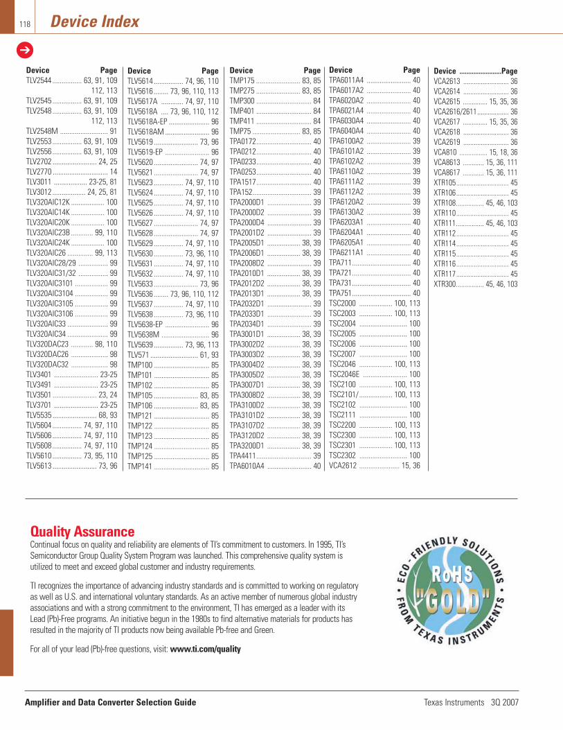
Amplifier and Data Converter Selection Guide Texas Instruments 3Q 2007
Device Index118
Device PageTLV2544 ................ 63, 91, 109
112, 113TLV2545 ................ 63, 91, 109TLV2548 ................ 63, 91, 109
112, 113TLV2548M .......................... 91TLV2553 ................ 63, 91, 109TLV2556 ................ 63, 91, 109TLV2702 ........................ 24, 25TLV2770 .............................. 14TLV3011 .................. 23-25, 81TLV3012 .................. 24, 25, 81TLV320AIC12K .................. 100TLV320AIC14K .................. 100TLV320AIC20K .................. 100TLV320AIC23B ............ 99, 110TLV320AIC24K .................. 100TLV320AIC26 .............. 99, 113TLV320AIC28/29 ................ 99TLV320AIC31/32 ................ 99TLV320AIC3101 .................. 99TLV320AIC3104 .................. 99TLV320AIC3105 .................. 99TLV320AIC3106 .................. 99TLV320AIC33 ...................... 99TLV320AIC34 ...................... 99TLV320DAC23 ............ 98, 110TLV320DAC26 .................... 98TLV320DAC32 .................... 98TLV3401 ........................ 23-25TLV3491 ........................ 23-25TLV3501 ........................ 23, 24TLV3701 ........................ 23-25TLV5535 ........................ 68, 93TLV5604 ................ 74, 97, 110TLV5606 ................ 74, 97, 110TLV5608 ................ 74, 97, 110TLV5610 ................ 73, 95, 110TLV5613 ........................ 73, 96
Device PageTLV5614 ................ 74, 96, 110TLV5616........ 73, 96, 110, 113TLV5617A ............ 74, 97, 110TLV5618A .... 73, 96, 110, 112TLV5618A-EP ...................... 96TLV5618AM ........................ 96TLV5619 ........................ 73, 96TLV5619-EP ........................ 96TLV5620 ........................ 74, 97TLV5621 ........................ 74, 97TLV5623 ................ 74, 97, 110TLV5624 ................ 74, 97, 110TLV5625 ................ 74, 97, 110TLV5626 ................ 74, 97, 110TLV5627 ........................ 74, 97TLV5628 ........................ 74, 97TLV5629 ................ 74, 97, 110TLV5630 ................ 73, 96, 110TLV5631 ................ 74, 97, 110TLV5632 ................ 74, 97, 110TLV5633 ........................ 73, 96TLV5636........ 73, 96, 110, 112TLV5637 ................ 74, 97, 110TLV5638 ................ 73, 96, 110TLV5638-EP ........................ 96TLV5638M .......................... 96TLV5639 ................ 73, 96, 113TLV571 .......................... 61, 93TMP100 .............................. 85TMP101 .............................. 85TMP102 .............................. 85TMP105 ........................ 83, 85TMP106 ........................ 83, 85TMP121 .............................. 85TMP122 .............................. 85TMP123 .............................. 85TMP124 .............................. 85TMP125 .............................. 85TMP141 .............................. 85
Device PageTMP175 ........................ 83, 85TMP275 ........................ 83, 85TMP300 .............................. 84TMP401 .............................. 84TMP411 .............................. 84TMP75 .......................... 83, 85TPA0172.............................. 40TPA0212.............................. 40TPA0233.............................. 40TPA0253.............................. 40TPA1517.............................. 40TPA152................................ 39TPA2000D1 ........................ 39TPA2000D2 ........................ 39TPA2000D4 ........................ 39TPA2001D2 ........................ 39TPA2005D1 .................. 38, 39TPA2006D1 .................. 38, 39TPA2008D2 ........................ 39TPA2010D1 .................. 38, 39TPA2012D2 .................. 38, 39TPA2013D1 .................. 38, 39TPA2032D1 ........................ 39TPA2033D1 ........................ 39TPA2034D1 ........................ 39TPA3001D1 .................. 38, 39TPA3002D2 .................. 38, 39TPA3003D2 .................. 38, 39TPA3004D2 .................. 38, 39TPA3005D2 .................. 38, 39TPA3007D1 .................. 38, 39TPA3008D2 .................. 38, 39TPA3100D2 .................. 38, 39TPA3101D2 .................. 38, 39TPA3107D2 .................. 38, 39TPA3120D2 .................. 38, 39TPA3200D1 .................. 38, 39TPA4411.............................. 39TPA6010A4 ........................ 40
Device PageTPA6011A4 ........................ 40TPA6017A2 ........................ 40TPA6020A2 ........................ 40TPA6021A4 ........................ 40TPA6030A4 ........................ 40TPA6040A4 ........................ 40TPA6100A2 ........................ 39TPA6101A2 ........................ 39TPA6102A2 ........................ 39TPA6110A2 ........................ 39TPA6111A2 ........................ 39TPA6112A2 ........................ 39TPA6120A2 ........................ 39TPA6130A2 ........................ 39TPA6203A1 ........................ 40TPA6204A1 ........................ 40TPA6205A1 ........................ 40TPA6211A1 ........................ 40TPA711................................ 40TPA721................................ 40TPA731................................ 40TPA751................................ 40TSC2000 .................. 100, 113TSC2003 .................. 100, 113TSC2004 .......................... 100TSC2005 .......................... 100TSC2006 .......................... 100TSC2007 .......................... 100TSC2046 .................. 100, 113TSC2046E ........................ 100TSC2100 .................. 100, 113TSC2101/.................. 100, 113TSC2102 .......................... 100TSC2111 .......................... 100TSC2200 .................. 100, 113TSC2300 .................. 100, 113TSC2301 .................. 100, 113TSC2302 .......................... 100VCA2612 ...................... 15, 36
Device ........................PageVCA2613 .......................... 36VCA2614 .......................... 36VCA2615 .............. 15, 35, 36VCA2616/2611.................. 36VCA2617 .............. 15, 35, 36VCA2618 .......................... 36VCA2619 .......................... 36VCA810 ................ 15, 18, 36VCA8613 ............ 15, 36, 111VCA8617 ............ 15, 36, 111XTR105.............................. 45XTR106.............................. 45XTR108................ 45, 46, 103XTR110.............................. 45XTR111................ 45, 46, 103XTR112.............................. 45XTR114.............................. 45XTR115.............................. 45XTR116.............................. 45XTR117.............................. 45XTR300................ 45, 46, 103
Quality AssuranceContinual focus on quality and reliability are elements of TI’s commitment to customers. In 1995, TI’sSemiconductor Group Quality System Program was launched. This comprehensive quality system is utilized to meet and exceed global customer and industry requirements.
TI recognizes the importance of advancing industry standards and is committed to working on regulatoryas well as U.S. and international voluntary standards. As an active member of numerous global industryassociations and with a strong commitment to the environment, TI has emerged as a leader with itsLead (Pb)-Free programs. An initiative begun in the 1980s to find alternative materials for products hasresulted in the majority of TI products now being available Pb-free and Green.
For all of your lead (Pb)-free questions, visit: www.ti.com/quality

Texas Instruments 3Q 2007 Amplifier and Data Converter Selection Guide
Resources
Product Information Centers
119
© 2007 Texas Instruments IncorporatedPrinted in U.S.A. by Jarvis Press, Dallas, Texas
Printed on recycled paper
Trademarks in this guide: Technology for Innovators and the black/red banner, PowerPAD, Difet, Excalibur, e-trim, MicroAmplifier, DaVinci, OMAP, PurePath Digital, Direct Path, MicroStar Junior,TMS320, FilterPro, SARdriverPro, MDACBUFFERPro, Code Composer Studio, C28x, C54x, C55x, C62x,C64x, C67x, C6000, NanoStar, NanoFree, TINA-TI and ADCPro are trademarks of Texas Instruments.All other trademarks are the property of their respective owners.
TI Worldwide Technical Support
InternetTI Semiconductor Product Information Center HomePagesupport.ti.com
TI Semiconductor KnowledgeBase Home Pagesupport.ti.com/sc/knowledgebase
Product Information CentersAmericasPhone +1(972) 644-5580Fax +1(972) 927-6377Internet/Email support.ti.com/sc/pic/americas.htm
Europe, Middle East, and AfricaPhone
European Free Call 00800-ASK-TEXAS(00800 275 83927)
International +49 (0) 8161 80 2121Russian Support +7 (4) 95 98 10 701
Note: The European Free Call (Toll Free) number is not active in allcountries. If you have technical difficulty calling the free call num-ber, please use the international number above.
Fax +(49) (0) 8161 80 2045Internet support.ti.com/sc/pic/euro.htm
JapanFax International +81-3-3344-5317
Domestic 0120-81-0036
Internet/Email International support.ti.com/sc/pic/japan.htmDomestic www.tij.co.jp/pic
AsiaPhone
International +886-2-23786800Domestic Toll-Free Number
Australia 1-800-999-084China 800-820-8682Hong Kong 800-96-5941India +91-80-41381665 (Toll)Indonesia 001-803-8861-1006Korea 080-551-2804Malaysia 1-800-80-3973New Zealand 0800-446-934Philippines 1-800-765-7404Singapore 800-886-1028Taiwan 0800-006800Thailand 001-800-886-0010
Fax +886-2-2378-6808Email [email protected] or [email protected] support.ti.com/sc/pic/asia.htm
Important Notice: The products and services of Texas Instruments Incorporated andits subsidiaries described herein are sold subject to TI’s standard terms andconditions of sale. Customers are advised to obtain the most current and completeinformation about TI products and services before placing orders. TI assumes noliability for applications assistance, customer’s applications or product designs,software performance, or infringement of patents. The publication of informationregarding any other company’s products or services does not constitute TI’s approval,warranty or endorsement thereof.
Safe Harbor Statement: This publication may contain forward-looking statements thatinvolve a number of risks and uncertainties. These “forward-looking statements” areintended to qualify for the safe harbor from liability established by the Private SecuritiesLitigation Reform Act of 1995. These forward-looking statements generally can beidentified by phrases such as TI or its management “believes,” “expects,” “anticipates,”“foresees,” “forecasts,” “estimates” or other words or phrases of similar import.Similarly, such statements herein that describe the company's products, businessstrategy, outlook, objectives, plans, intentions or goals also are forward-lookingstatements. All such forward-looking statements are subject to certain risks anduncertainties that could cause actual results to differ materially from those in forward-looking statements. Please refer to TI's most recent Form 10-K for more information onthe risks and uncertainties that could materially affect future results of operations. Wedisclaim any intention or obligation to update any forward-looking statements as a resultof developments occurring after the date of this publication.
E062907

PRSRT STDU.S. POSTAGE
PAIDDALLAS, TEXAS
PERMIT NO. 2758
Texas Instruments Incorporated
14950 FAA Blvd.
Fort Worth, Texas 76155-9951
Address service requested
SLYB115B
IMPORTANT NOTICE
Texas Instruments Incorporated and its subsidiaries (TI) reserve the right to make corrections, modifications, enhancements,improvements, and other changes to its products and services at any time and to discontinue any product or service without notice.Customers should obtain the latest relevant information before placing orders and should verify that such information is current andcomplete. All products are sold subject to TI’s terms and conditions of sale supplied at the time of order acknowledgment.
TI warrants performance of its hardware products to the specifications applicable at the time of sale in accordance with TI’sstandard warranty. Testing and other quality control techniques are used to the extent TI deems necessary to support thiswarranty. Except where mandated by government requirements, testing of all parameters of each product is not necessarilyperformed.
TI assumes no liability for applications assistance or customer product design. Customers are responsible for their products andapplications using TI components. To minimize the risks associated with customer products and applications, customers shouldprovide adequate design and operating safeguards.
TI does not warrant or represent that any license, either express or implied, is granted under any TI patent right, copyright, maskwork right, or other TI intellectual property right relating to any combination, machine, or process in which TI products or servicesare used. Information published by TI regarding third-party products or services does not constitute a license from TI to use suchproducts or services or a warranty or endorsement thereof. Use of such information may require a license from a third party underthe patents or other intellectual property of the third party, or a license from TI under the patents or other intellectual property of TI.
Reproduction of TI information in TI data books or data sheets is permissible only if reproduction is without alteration and isaccompanied by all associated warranties, conditions, limitations, and notices. Reproduction of this information with alteration is anunfair and deceptive business practice. TI is not responsible or liable for such altered documentation. Information of third partiesmay be subject to additional restrictions.
Resale of TI products or services with statements different from or beyond the parameters stated by TI for that product or servicevoids all express and any implied warranties for the associated TI product or service and is an unfair and deceptive businesspractice. TI is not responsible or liable for any such statements.
TI products are not authorized for use in safety-critical applications (such as life support) where a failure of the TI product wouldreasonably be expected to cause severe personal injury or death, unless officers of the parties have executed an agreementspecifically governing such use. Buyers represent that they have all necessary expertise in the safety and regulatory ramificationsof their applications, and acknowledge and agree that they are solely responsible for all legal, regulatory and safety-relatedrequirements concerning their products and any use of TI products in such safety-critical applications, notwithstanding anyapplications-related information or support that may be provided by TI. Further, Buyers must fully indemnify TI and itsrepresentatives against any damages arising out of the use of TI products in such safety-critical applications.
TI products are neither designed nor intended for use in military/aerospace applications or environments unless the TI products arespecifically designated by TI as military-grade or "enhanced plastic." Only products designated by TI as military-grade meet militaryspecifications. Buyers acknowledge and agree that any such use of TI products which TI has not designated as military-grade issolely at the Buyer's risk, and that they are solely responsible for compliance with all legal and regulatory requirements inconnection with such use.
TI products are neither designed nor intended for use in automotive applications or environments unless the specific TI productsare designated by TI as compliant with ISO/TS 16949 requirements. Buyers acknowledge and agree that, if they use anynon-designated products in automotive applications, TI will not be responsible for any failure to meet such requirements.
Following are URLs where you can obtain information on other Texas Instruments products and application solutions:
Products Applications
Amplifiers amplifier.ti.com Audio www.ti.com/audio
Data Converters dataconverter.ti.com Automotive www.ti.com/automotive
DSP dsp.ti.com Broadband www.ti.com/broadband
Interface interface.ti.com Digital Control www.ti.com/digitalcontrol
Logic logic.ti.com Military www.ti.com/military
Power Mgmt power.ti.com Optical Networking www.ti.com/opticalnetwork
Microcontrollers microcontroller.ti.com Security www.ti.com/security
RFID www.ti-rfid.com Telephony www.ti.com/telephony
Low Power www.ti.com/lpw Video & Imaging www.ti.com/videoWireless
Wireless www.ti.com/wireless
Mailing Address: Texas Instruments, Post Office Box 655303, Dallas, Texas 75265Copyright © 2007, Texas Instruments Incorporated