back propagation control algorithm for power quality...
TRANSCRIPT

ISSN (Print): 2328-3491, ISSN (Online): 2328-3580, ISSN (CD-ROM): 2328-3629
American International Journal of Research in Science, Technology, Engineering & Mathematics
AIJRSTEM 16-167; © 2016, AIJRSTEM All Rights Reserved Page 113
AIJRSTEM is a refereed, indexed, peer-reviewed, multidisciplinary and open access journal published by International Association of Scientific Innovation and Research (IASIR), USA
(An Association Unifying the Sciences, Engineering, and Applied Research)
Available online at http://www.iasir.net
Back Propagation Control Algorithm for Power Quality Improvement
Using DSTATCOM R.Ranjithkumar1,G.Arunsankar2
1Ph.D. Scholar (Meenakshi University, Chennai, Tamilnadu, INDIA) and Assistant Professor Gojan School of
Business & Technology, Edapalayam, Chennai, Tamil Nadu 600052, INDIA. 2Ph.D. Scholar (Anna University, Chennai, Tamilnadu, INDIA) and Associate Professor Gojan School of
Business & Technology, Edapalayam, Chennai, Tamil Nadu 600052, INDIA.
I. INTRODUCTION The project titled “Back-Propagation Control Algorithm for Power Quality Improvement Using DSTATCOM”
aimed at obtaining the control is carried out by the implementation of a three phase distribution static
compensator (DSTATCOM) using a back propagation (BP) control algorithm for its functions such as harmonic
elimination, load balancing and reactive power compensation for power factor correction, and zero voltage
regulation under nonlinear loads.
A BP-based control algorithm is used for the extraction of the fundamental weighted value of active and reactive
power components of load currents which are required for the estimation of reference source currents. Power
converter based custom power devices (CPDs) are useful for reduction of power quality problems such as power
factor correction, harmonics compensation, voltage sag/swell compensation, resonance due to distortion, voltage
flicker reduction within specified. These CPDs include DSTATCOM, DVR and UPQC in different
Configurations. Many non model and training based alternative control algorithms are reported in the literature
with application of soft computing technique such as neural network, fuzzy logic and adaptive neuro-fuzzy etc,.
For better power quality improvement as power factor correction and to maintain rated PCC voltage a VSC
based DSTATCOM has been introduced. A prototype of DSTATCOM is developed using a digital signal
processor, and its performance is studied under various operating conditions.
II. OPTIMAL PLACEMENT OF DSTATCOM IN AN INDIAN POWER SYSTEM
FOR LOAD AND VOLTAGE BALANCING Power quality is of increasing importance in worldwide distribution. The present distribution systems are facing
severe power quality problems such as poor voltage regulation, high reactive power demand, harmonics in
supply voltage and current, and load unbalancing. Therefore, maintenance of power quality is becoming of
increasing importance in worldwide distribution systems. Industrial consumers with more automated processes
require high quality power supply else equipments such as microcontrollers, computers and motor drives may
get damaged. High quality power delivery includes balanced voltage supply to consumers. Connection of
unbalanced load at a bus may cause unbalanced voltage and current drawn by other loads connected at that bus.
Switching of unbalanced load at a bus may also result in unbalanced voltage at some other buses.
Unbalanced voltages contain negative and zero sequence components which may cause additional losses in
motors and generators, oscillating torques in Alternating Current (AC) machines, increased ripples in rectifiers,
saturation of transformers, excessive neutral currents and malfunctioning of several type of equipments. With
Abstract: This paper “Back-Propagation Control Algorithm for Power Quality Improvement Using
DSTATCOM” presents an implementation of three- phase Distribution Static Compensator (DSTATCOM)
using back-propagation (BP) control algorithm for its functions such as harmonics elimination, load
balancing and reactive power compensation for power factor correction (PFC) and zero voltage regulation
(ZVR) under nonlinear loads. A BP based control algorithm is used for extraction of fundamental weighted
value of active and reactive power components of load currents which are required for estimation of
reference source currents. Power converter based custom power devices (CPDs) are useful for reduction of
power quality problems such as power factor correction, harmonics compensation, voltage sag/swell
compensation, resonance due to distortion, voltage flicker reduction within specified limits. These CPDs
include DSTATCOM, DVR and UPQC in different Configurations. Many non model and training based
alternative control algorithms are reported in the literature with application of soft computing technique
such as neural network, fuzzy logic and adaptive neuro-fuzzy etc,. For better power quality improvement as
power factor correction and to maintain rated PCC voltage A VSC based DSTATCOM has been introduced.
Keywords: DSTATCOM, power factor correction, zero voltage regulation

R.Ranjithkumar et al., American International Journal of Research in Science, Technology, Engineering & Mathematics, 14(2), March-
May, 2016, pp. 113-121
AIJRSTEM 16-167; © 2016, AIJRSTEM All Rights Reserved Page 114
the advancement in power electronics, new controllers known as Flexible AC Transmission System (FACTS)
have been developed. These controllers have been proved to be quite effective in power flow control, reactive
power compensation and enhancement of stability margin in AC networks. Power electronics based controllers
used in distribution systems are called custom power devices. Custom power devices have been proved to be
quite effective in power quality enhancement. The custom power devices may be series, shunt, and series-shunt
or series-series type depending upon their connection in the circuit. Most prominent custom power devices
include Distribution Static Compensator (DSTATCOM), Dynamic Voltage Restorer (DVR) and Unified Power
Quality Conditioner (UPQC). There are several papers reported in literature on placement of custom power
devices in balancing of unbalanced load in radial distribution systems. Load voltage balancing using DVR
against unbalanced supply voltage in radial distribution system has been considered. Placement of DSTATCOM
in weak AC radial distribution system for load voltage and current balancing has been considered in . Balancing
of source currents using DSTATCOM in radial distribution system has been considered in. Unbalancing has
been caused by connection of unbalanced and non-linear load. Load compensation using DSTATCOM against
unbalancing caused by opening of one of the phase of the load in radial distribution system has been considered.
Balancing of supply across an unbalanced 4- phase load along with power factor improvement using
DSTATCOM has been suggested. A Voltage Source Converter (VSC) based controller has been proposed to
balance terminal voltage of an isolated standalone asynchronous generator driven by constant speed prime
mover. A non-linear and unbalanced load has been connected at the generator terminals to create unbalance in
supply voltages. The paper uses three phase four wire four leg VSC topology for a DSTATCOM application.
III. DSTATCOM MODEL
In the present work, DSTATCOM has been represented as three independently controllable single phase current
sources injecting reactive current in the three phases at the point of coupling. The proposed DSTATCOM model
has been shown in figure 2.1. The control scheme consists of three control switches which can be set on/off as
per compensation requirement.
Fig. 2.2 Proposed DSTATCOM Model
IV. Back-Propagation Control Algorithm for Power Quality Improvement Using DSTATCOM
A voltage source converter (VSC)-based DSTATCOM is connected to a three phase ac mains feeding three
phase linear/nonlinear loads with internal grid impedance which is shown in Fig. 3.1. The performance of
DSTATCOM depends upon the accuracy of harmonic current detection. For reducing ripple in compensating
currents, the tuned values of interfacing inductors (Lf ) are connected at the ac output of the VSC. A three phase
series combination of capacitor (Cf ) and a resistor (Rf ) represents the shunt passive ripple filter which is
connected at a point of common coupling (PCC) for reducing the high frequency switching noise of the VSC.
The DSTATCOM currents (iCabc) are injected as required compensating currents to cancel the reactive power
components and harmonics of the load currents so that loading due to reactive power component/harmonics is
reduced on the distribution system. For the considered three phase nonlinear load with approximately 24 kW,
the compensator data are given in Appendix A.
Fig. 2.3 Schematic Diagram of VSC-Based DSTATCOM.

R.Ranjithkumar et al., American International Journal of Research in Science, Technology, Engineering & Mathematics, 14(2), March-
May, 2016, pp. 113-121
AIJRSTEM 16-167; © 2016, AIJRSTEM All Rights Reserved Page 115
V. PERFORMANCE OF DSTATCOM
MATLAB with SIMULINK and Sim Power System toolboxes is used for the development of the simulation
model of a DSTATCOM and its control algorithm. The performance of the BP algorithm in the time domain for
the three phase DSTATCOM is simulated for PFC and ZVR modes of operation under nonlinear loads. The
performance of the control algorithm is observed under nonlinear loads.
The dynamic performance of a VSC-based DSTATCOM is studied for PFC mode at nonlinear loads. The
performance indices are the phase voltages at PCC (vs), balanced source currents (is), load currents (iLa, iLb,
and iLc), compensator currents (iCa, iCb, and iCc), and dc bus voltage (Vdc) which are shown in Fig. 3.1 under
varying load (at t = 3.7 to 3.8 s) conditions.
Fig. 3.1 Dynamic Performance Of DSTATCOM Under Varying Nonlinear Loads In PFC Mode.
VI. SIMULATION RESULTS
Fig. 4.1 Circuit Diagram of Open Loop Method of Grid Connected System With PWM Control Method
The circuit diagram shown in the figure 4.2 explains the open loop method of grid connected system with PWM
control method. The circuit has six switching devices with their respective control signals. Moreover, the circuit
has load at the end.
Fig. 4.2. Input Voltage

R.Ranjithkumar et al., American International Journal of Research in Science, Technology, Engineering & Mathematics, 14(2), March-
May, 2016, pp. 113-121
AIJRSTEM 16-167; © 2016, AIJRSTEM All Rights Reserved Page 116
An input voltage of 400v for PWM inverter is shown in the figure 4.3. The time in seconds and voltage in volts
are plotted along x-axis and y-axis respectively.
Fig. 4.3 Switching Pulse For Inverter(M1,M3,M5)
The graph depicted shows the switching pulses for the PWM invertor. The switching devices used are MOSFET.
The time in seconds and amplitude in volts are plotted along x-axis and y-axis respectively.
Fig. 4.4 Output Voltage
The output voltage of grid connected system is shown in the figure 4.5. The voltage in volts is plotted in y-axis
and time in seconds is plotted in x-axis. At the time of 0.6 second load 2 gets switched ON and the voltage of
load 1 becomes sag.
Fig. 4.5 Output Current
The figure 4.6 shows the output current of grid connected system. The time in seconds is plotted in x-axis and
current in ampere is plotted in y-axis. Initially the value of current is one ampere. At the time of switching ON
the load 2, the output current of load 1 is reduced to zero
Fig. 4.6 Critical Load Output Voltage
The critical non-linear load output voltage of grid connected system is shown in the fig 4.7. The time in seconds
and voltage in volts are plotted along x-axis and y-axis respectively.

R.Ranjithkumar et al., American International Journal of Research in Science, Technology, Engineering & Mathematics, 14(2), March-
May, 2016, pp. 113-121
AIJRSTEM 16-167; © 2016, AIJRSTEM All Rights Reserved Page 117
Fig. 4.7 Total Harmonic Distortion (THD)
The graph in the fig 5.8 shows the Total Harmonic Distortion (THD) of output current for the grid connected
system. The order of harmonics is plotted along x-axis and magnitude (% of fundamentals) along y- axis.
Fig. 4.8 Circuit Diagram of Closed Loop Method of Grid Connected System with PWM Control Method
The circuit diagram shown in the figure 4.8 explains the closed loop method of grid connected system with
PWM control method. The circuit has six switching devices with their respective control signals. Moreover, the
circuit has load at the end.
Fig. 4.9 Input Voltage
An input voltage of 400v for PWM inverter is shown in the figure 4.9. The time in seconds and voltage in volts
are plotted along x-axis and y-axis respectively.
Fig. 4.10 Switching Pulse For (M1,M3,M5)
The figure 4.10 depicted shows the switching pulses for the PWM invertor. The switching devices used are
MOSFET. The time in seconds and amplitude in volts are plotted along x-axis and y-axis respectively.
R.Ranjithkumar et al., American International Journal of Research in Science, Technology, Engineering & Mathematics, 14(2), March-
May, 2016, pp. 113-121
AIJRSTEM 16-167; © 2016, AIJRSTEM All Rights Reserved Page 118
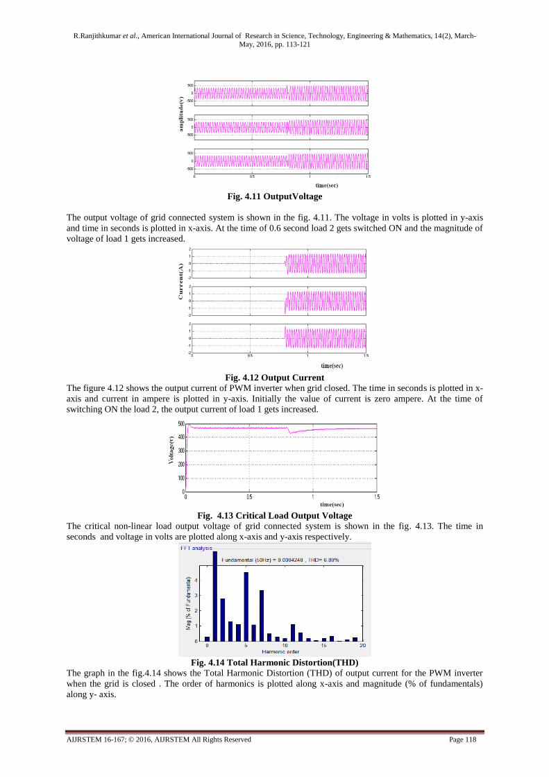
Fig. 4.11 OutputVoltage
The output voltage of grid connected system is shown in the fig. 4.11. The voltage in volts is plotted in y-axis
and time in seconds is plotted in x-axis. At the time of 0.6 second load 2 gets switched ON and the magnitude of
voltage of load 1 gets increased.
Fig. 4.12 Output Current
The figure 4.12 shows the output current of PWM inverter when grid closed. The time in seconds is plotted in x-
axis and current in ampere is plotted in y-axis. Initially the value of current is zero ampere. At the time of
switching ON the load 2, the output current of load 1 gets increased.
Fig. 4.13 Critical Load Output Voltage
The critical non-linear load output voltage of grid connected system is shown in the fig. 4.13. The time in
seconds and voltage in volts are plotted along x-axis and y-axis respectively.
Fig. 4.14 Total Harmonic Distortion(THD)
The graph in the fig.4.14 shows the Total Harmonic Distortion (THD) of output current for the PWM inverter
when the grid is closed . The order of harmonics is plotted along x-axis and magnitude (% of fundamentals)
along y- axis.

R.Ranjithkumar et al., American International Journal of Research in Science, Technology, Engineering & Mathematics, 14(2), March-
May, 2016, pp. 113-121
AIJRSTEM 16-167; © 2016, AIJRSTEM All Rights Reserved Page 119
Fig. 4.15 Cicuit Diagram With Grid Closed Space Vector Modulation(Svm) Control Method
Space Vector Modulation is an algrothim for the control of pulse width modulation. It is used for the creation of
alternate current(AC) waveforms; most commenly to drive three phase AC powered motors at varying speeds
from DC using multiple class D amplifiers. There are various variations of SVM that result different quality and
computational requirements. One active area of development is in the reduction of total harmonic distortion
created by the rapid switching inherent to this algroithm. To implement SVM, a reference signal Vref is sampled
with a frequency fs. the reference signal may be generated from three separate phase reference. The reference
vector is then sythensized using a combination of the two adjcent active switching vectors and one or both zero
vectors.
Fig. 4.16 Input Voltage
An input voltage of 400v for SVM inverter is shown in the fig. 4.16. The time in seconds and voltage in volts
are plotted along x-axis and y-axis respectively.
Fig. 4.17 Switching Pulse for M1,M3, M5
The graph depicted shows the switching pulses for the SVM invertor. The switching devices used are MOSFET.
The time in seconds and amplitude in volts are plotted along x-axis and y-axis respectively.
Fig. 4.18 Output Voltage

R.Ranjithkumar et al., American International Journal of Research in Science, Technology, Engineering & Mathematics, 14(2), March-
May, 2016, pp. 113-121
AIJRSTEM 16-167; © 2016, AIJRSTEM All Rights Reserved Page 120
The output voltage of SVM inverter is shown in the fig. 4.19. The voltage in volts is plotted in y-axis and time
in seconds is plotted in x-axis. At the time of 0.6 second load 2 gets switched ON and the magnitude of voltage
of load 1 gets increased.
Fig. 4.19 Output Current
The figure 4.20 shows the output current of PWM inverter when grid closed. The time in seconds is plotted in x-
axis and current in ampre is plotted in y-axis. Initially the value of current is zero ampre. At the time of
switching ON the load 2, the output current of load 1 gets increased.
Fig. 4.20 Critical Load Output Voltage
The critical non-linear load output voltage of grid connected system is shown in the fig. 4.21. The time in
seconds and voltage in volts are plotted along x-axis and y-axis respectively.
Fig. 4.21 Total Harmonic Distortion(THD)
The graph in the fig 4.21 shows the Total Harmonic Distortion (THD) of output current for the SVM inverter.
The order of harmonics is plotted along x-axis and maginitude (% of fundamentals) along y- axis. It is evident
from the diagram the usage of SVM method enables us getting reduced harmonic in the order of 6.80% integrate.
VII. CONCLUSION
This project has presented the procedures for Back-Propagation Control Algorithm for Power Quality
Improvement Using DSTATCOM system. A VSC-based DSTATCOM has been accepted as the most preferred
solution for power quality improvement as PFC and to maintain rated PCC voltage. A three phase DSTATCOM
has been implemented for the compensation of nonlinear loads. Performance of DSTATCOM under nonlinear
loads: (a-c) isa, isb, and isc with vab; (d-f) iLa, iLb, and iLc; and (g-i) iCa, iCb, and iCc. (j-l) Harmonic spectra
of isa, iLa, and vab. ing a BPT control algorithm to verify its effectiveness. The proposed BPT control algorithm
has been used for the extraction of reference source currents to generate the switching pulses for IGBTs of the
VSC of DSTATCOM. Various functions of DSTATCOM such as harmonic elimination and load balancing
have been demonstrated in PFC and ZVR modes with dc voltage regulation of DSTATCOM. From the
simulation and implementation results, it is concluded that DSTATCOM and its control algorithm have been

R.Ranjithkumar et al., American International Journal of Research in Science, Technology, Engineering & Mathematics, 14(2), March-
May, 2016, pp. 113-121
AIJRSTEM 16-167; © 2016, AIJRSTEM All Rights Reserved Page 121
found suitable for the compensation of nonlinear loads. Its performance has been found satisfactory for this
application because the extracted reference source currents exactly traced the sensed source currents during the
steady state as well as dynamic conditions. The dc bus voltage of the DSTATCOM has also been regulated to
the rated value without any overshoot or undershoot during load variation. Large training time in the application
of the complex system and the selection of the number of hidden layers in the system are the disadvantages of
this algorithm. The Basic circuit and modified circuit elements are designed using relevant equations. The
simulation circuits are developed using elements of simulink library. The Simulation is successfully done and
open loop / closed loop simulation results are presented. The Simulation results coincide with the theoretical
results.
REFERENCES [1] R. C. Dugan, M. F. McGranaghan, and H. W. Beaty, Electric Power Systems Quality, 2nd ed. New York, NY, USA: McGraw-
Hill, 2006. [2] A. Ortiz, C. Gherasim, M. Manana, C. J. Renedo, L. I. Eguiluz, and R. J. M. Belmans, “Total harmonic distortion decomposition
depending on distortion origin,” IEEE Trans. Power Del., vol. 20, no. 4, pp. 2651–2656, Oct. 2005.
[3] T. L. Lee and S. H. Hu, “Discrete frequency-tuning active filter to suppress harmonic resonances of closed-loop distribution power systems,” IEEE Trans. Power Electron., vol. 26, no. 1, pp. 137–148, Jan. 2011.
[4] K. R. Padiyar, FACTS Controllers in Power Transmission and Distribution. New Delhi, India: New Age Int., 2008.
[5] IEEE Recommended Practices and Requirement for Harmonic Control on Electric Power System, IEEE Std.519, 1992. [6] T.-L. Lee, S.-H. Hu, and Y.-H. Chan, “DSTATCOM with positivesequence admittance and negative-sequence conductance to
mitigate voltage fluctuations in high-level penetration of distributed generation systems,” IEEE Trans. Ind. Electron., vol. 60, no.
4, pp. 1417–1428, Apr. 2013. [7] B. Singh, P. Jayaprakash, and D. P. Kothari, “Power factor correction and power quality improvement in the distribution
system,” Elect. India Mag., pp. 40–48, Apr. 2008.
[8] J.-C. Wu, H. L. Jou, Y. T. Feng, W. P. Hsu, M. S. Huang, and W. J. Hou, “Novel circuit topology for three-phase active power filter,” IEEE Trans. Power Del., vol. 22, no. 1, pp. 444–449, Jan. 2007.
[9] Z. Yao and L. Xiao, “Control of single-phase grid-connected inverters with nonlinear loads,” IEEE Trans. Ind. Electron., vol. 60,
no. 4, pp. 1384– 1389, Apr. 2013. [10] A. A. Heris, E. Babaei, and S. H. Hosseini, “A new shunt active power filter based on indirect matrix converter,” in Proc. 20th
Iranian Conf. Elect. Eng., 2012, pp. 581–586.
[11] M. Sadeghi, A. Nazarloo, S. H. Hosseini, and E. Babaei, “A new DSTATCOM topology based on stacked multicell converter,” in Proc. 2nd Power Electron., Drive Syst. Technol. Conf., 2011, pp. 205–210.