bandgap reference circuit baased on finfet device
TRANSCRIPT

Design A New Stable And Low Power Bandgap Reference Circuit Based On Fin-FET Device
Yalagoud A. Patil
OUTLINE
• Introduction
• FinFET
• Architecture of the Bandgap
• Cascode OpAmp
• Circuit Analysis
• Simulations and features of selected bandgap
• Conclusion
INTRODUCTION
• What is Bandgap reference?
• Applications
• Temperature dependence of a PTAT circuit .
• Innovative techniques used to decrease voltage so as can be scaled down
with the technology scaling.
1. Use of resistive subdivision technique with native transistors or diodes.
2. Use a new technology to implement analog circuit such as FinFET based bandgap.
• There are more problems in order to design BGR in FinFET technology
rather than conventional CMOS structures.
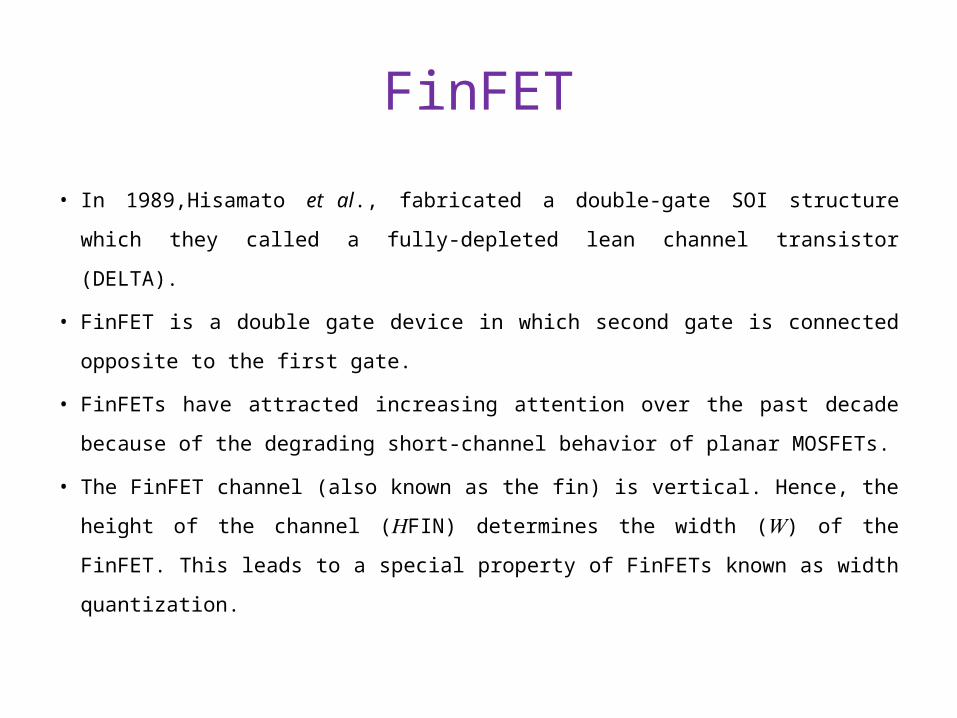
FinFET
• In 1989,Hisamato et al., fabricated a double-gate SOI structure which they
called a fully-depleted lean channel transistor (DELTA).
• FinFET is a double gate device in which second gate is connected opposite to
the first gate.
• FinFETs have attracted increasing attention over the past decade because of the
degrading short-channel behavior of planar MOSFETs.
• The FinFET channel (also known as the fin) is vertical. Hence, the height of
the channel ( FIN) determines the width ( ) of the FinFET. This leads to a 𝐻 𝑊
special property of FinFETs known as width quantization.
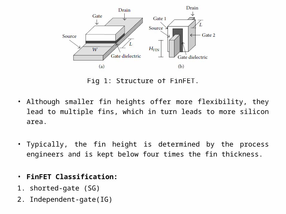
Fig 1: Structure of FinFET.
• Although smaller fin heights offer more flexibility, they lead to multiple fins, which in turn leads to more silicon area.
• Typically, the fin height is determined by the process engineers and is kept below four times the fin thickness.
• FinFET Classification:
1. shorted-gate (SG)
2. Independent-gate(IG)
Architecture of the Bandgap
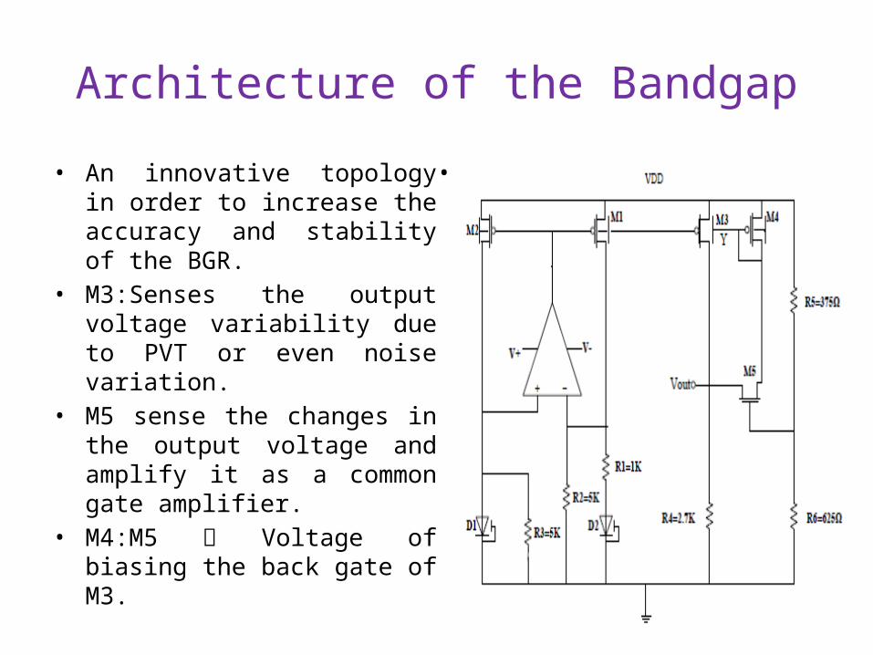
• An innovative topology in order to increase the accuracy and stability of the BGR.
• M3:Senses the output voltage variability due to PVT or even noise variation.
• M5 sense the changes in the output voltage and amplify it as a common gate amplifier.
• M4:M5 Voltage of biasing the back gate of M3.
• The difference between multiple VD of two diodes changes Proportional to Absolute Temperature (PTAT).
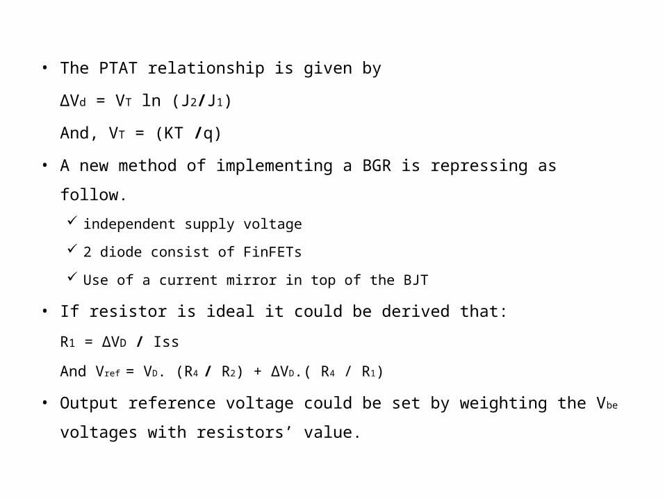
• The PTAT relationship is given by
ΔVd = VT ln (J2/J1)
And, VT = (KT /q)
• A new method of implementing a BGR is repressing as follow.
independent supply voltage
2 diode consist of FinFETs
Use of a current mirror in top of the BJT
• If resistor is ideal it could be derived that:
R1 = ΔVD / Iss
And Vref = VD. (R4 / R2) + ΔVD.( R4 / R1)
• Output reference voltage could be set by weighting the Vbe voltages with
resistors’ value.
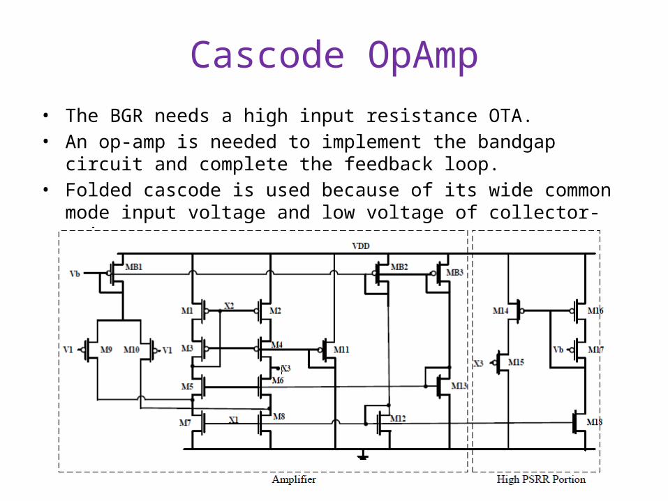
Cascode OpAmp• The BGR needs a high input resistance OTA.• An op-amp is needed to implement the bandgap circuit and complete the
feedback loop. • Folded cascode is used because of its wide common mode input voltage
and low voltage of collector-emitter.
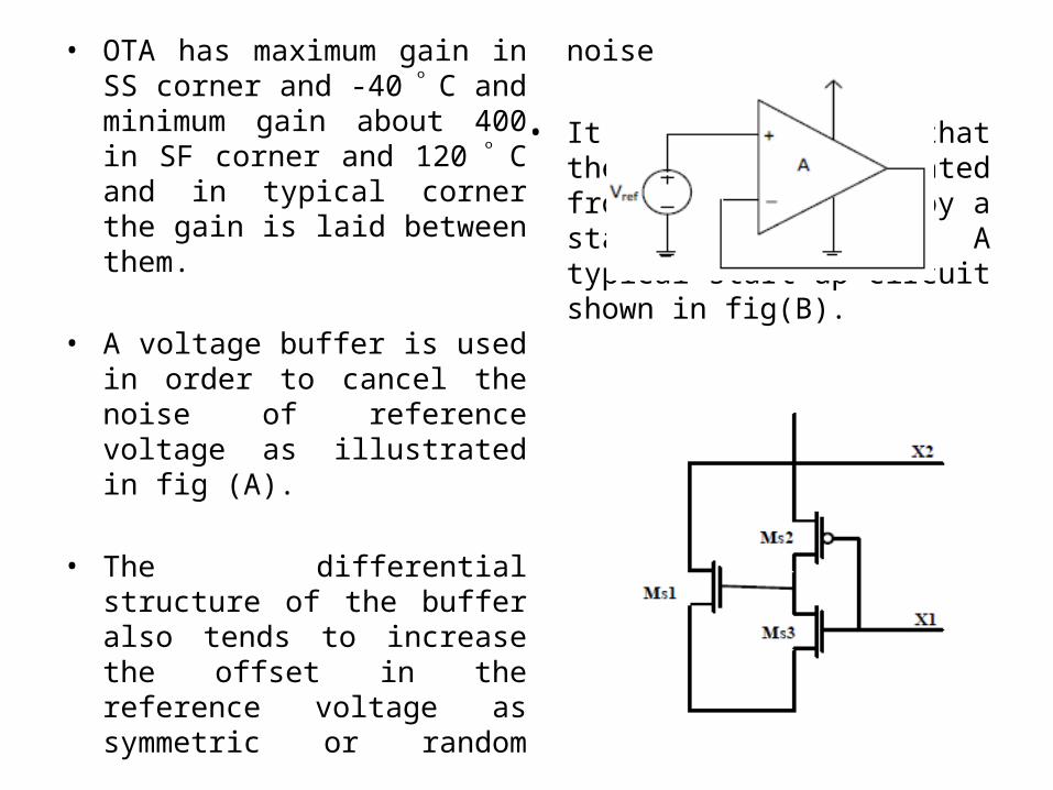
• OTA has maximum gain in SS corner and -40 ͦ C and minimum gain about 400 in SF corner and 120 ͦ C and in typical corner the gain is laid between them.
• A voltage buffer is used in order to cancel the noise of reference voltage as illustrated in fig (A).
• The differential structure of the buffer also tends to increase the offset in the reference voltage as symmetric or random noise
• It’s also required that the current initiated from its zero state by a start-up circuit. A typical start-up circuit shown in fig(B).
Circuit Analysis• The temperature coefficient of diodes voltage, it could be gained that:
∂Vd = − (0.6 / T) • Another assumption is the diode junction voltage is about 0.6 in 300˚K.
Vd2 = 0.6 V3 = V2 R2 = R3
ΔVd = R0Ic2 Iout = [VT ln (m)/ R1 + Vbe1/ R2] ∂Vref / ∂T = ∂ / ∂T[ R4( VT ln (m)/ R1 + Vd1 / R2]
• And for minimum sensitivity to temperature in 300˚Kit should be zero. ∂Vref /∂T = (R4Kqln (m) /R1) − (R4 / R2 × 0.6 / T) = 0
• By considering the m=100 for BJTs and also R4=2.7K we could find: R2 / R1 = 5
• For writing the feedback formulathe Rout of M5 should be find, this equation are as: RD5 = 1/gm4
• So the gain of feedback equal to: Af = gm5 x Rd Af = gm5 / gm4
Simulations and features of selected bandgap
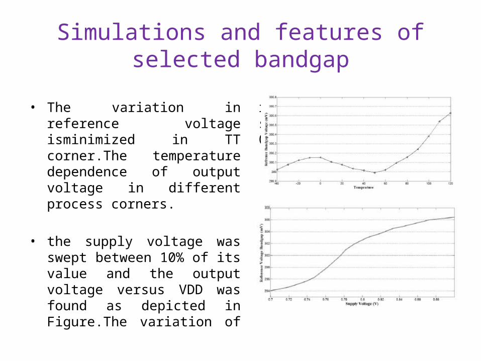
• The variation in reference voltage isminimized in TT corner.The temperature dependence of output voltage in different process corners.
• the supply voltage was swept between 10% of its value and the output voltage versus VDD was found as depicted in Figure.The variation of reference voltage under such variation is below 0.01%.

• In fig (A). The different values of Vref for variety of temperature and process corners which are result of variation in threshold voltages. The maximum variation for Vref is as low as 1.45mV
• Indeed using the Non-ideal resistors which are available in the technology in this method make this approach very attractive and easy to fab.
• An amplifier is used in order to regulate this voltage and keep it in the same value for both transistors. Fig (B) shows the effect of M1-M3 transistors in BGR voltage.
Fig (A) Fig (B)
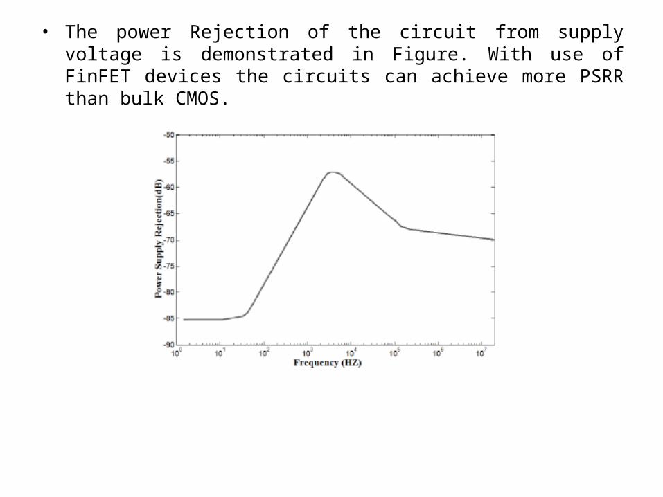
• The power Rejection of the circuit from supply voltage is demonstrated in Figure. With use of FinFET devices the circuits can achieve more PSRR than bulk CMOS.
Conclusion
• This architecture generate stable and regulate output voltage with using of extra feedback. This feedback makes circuit more stable against PVT variation and noise. Use of FinFET devices provide extra pin for controlling threshold voltage of this device by giving the voltage to back gate of it.
• It was tested with supply voltages between 0.7 and 0.9 volt and between -40 ͦ C and +120 ͦ C. this circuit generates a reference voltage of 300mV with only 0.041% and 0.01% variation versus Temperature and VDD variation respectively. 32nm PTM technology is used for simulation