bang-bang digital plls at 11 ghz and 20 ghz with … · 2 at t = 125°c, 8.4 ghz the rms jitter (5...
TRANSCRIPT
1
Bang-Bang Digital PLLs at 11 GHz and 20 GHz with sub-200-fs Integrated Jitter for High Speed Serial Communication
Applications
A. Rylyakov, J. Tierno, H. Ainspan, J.-O. Plouchart, Z. Toprak Deniz, J. Bulzacchelli, D. Friedman
IBM T.J. Watson Research Center, Yorktown Heights, NY

2
Motivation• Goal: demonstrate DPLL adequate for 8- to 11-Gbps and 17-
to 20-Gbps wireline communication applications:
– jitter (integrated from fc/1667 to fc/2) ~ 0.3 ps rms– bandwidth: ~ 1 MHz– integer-N: ~ 40
• A drop-in replacement for analog PLLs, offering:
– significant area savings– increased programmability– reduced analog content (models, variability, sensitivity)– portability to advanced CMOS technologies

3
Bang-bang DPLL Background
PK Z-D
proportional path gain, latency
LC-DCO
BB-PFD
÷N
+Z-1
Z-MIK
ΦOUTearly/lateΦREF
ΦFBK
Main design considerations:• PFD: bang-bang or TDC• Loop Filter: BB-PLL jitter grows with increase in proportional path gain (KP ) and latency (D)*• DCO: tuning range, fine tuning step (KDCO), phase noise
* Walker 1992, Da Dalt 2005, Hanumolu 2007

4
Bang-bang PFD vs TDC Integer-N LC-DPLL Verilog simulation results
Time [ns]200 400 600 800
-2
21
-10
1
0
Feedback phase errorΦREF − ΦFBK[ps]
Bang-bangPFD output
• Bang-bang PFD produces same output as 2 ps resolution TDC • Need sub-1ps resolution TDC to extract significantly more information than provided by BB-PFD
5
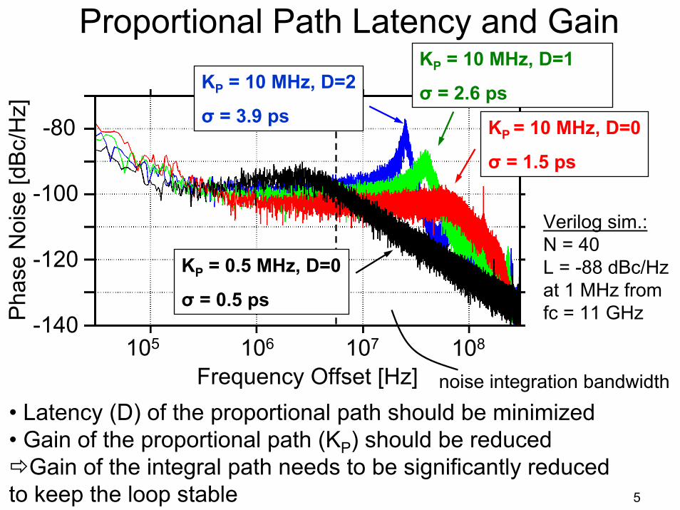
Proportional Path Latency and Gain
Frequency Offset [Hz]105 106 107 108
-140
KP = 10 MHz, D=1
σ = 2.6 ps
KP = 10 MHz, D=0
σ = 1.5 ps
KP = 0.5 MHz, D=0
σ = 0.5 ps
KP = 10 MHz, D=2
σ = 3.9 ps
Verilog sim.:N = 40L = -88 dBc/Hzat 1 MHz fromfc = 11 GHz
noise integration bandwidth
Pha
se N
oise
[dB
c/H
z]
-100
-120
-80
• Latency (D) of the proportional path should be minimized• Gain of the proportional path (KP) should be reduced
Gain of the integral path needs to be significantly reducedto keep the loop stable

6
BB-DPLL Block Diagramfractional delay bits prop path gain, type
LC
TANK
DCO
output BB-PFD
reference
DELAY
2
dithered reference
INT ∆ΣM8
inc/dec
∆ΣM
ROW-COL
early/lateSEL
delay line controls
EN1 … EN7
4coarse
8 12pcap
48
7icap
1
frac ditherearly/late
1/N 1/4 or 1/16phold clkgdelay range

7
11 GHz, 20 GHz LC DCO Topology
VDDAVDDA
<1:6>
<1:48>
IREF
output
output_b
pcap<6:12> pcap<6:12><6:12>
fine tuning steps KDCO
metal-metal overlap
varactors with size offsets
KP
coarse <1:4> <1:4>
icap <1:48>
dither, pcap<1:5>
<6:12>
to prescalerMain design challenges:• preserving oscillator Q while meeting tuning range and KDCO requirements• realizing low-gain KP

8
LC-DCO Coarse Band Tuning Ranges
8
9
10
11
12
1 4 8 12 16
Freq
uenc
y [G
Hz]
DCO Coarse Tuning Band Number
11 GHz DCO 20 GHz DCO
22
20
18
168 12 16
KDCO = 6 MHz − 14 MHz KDCO = 16 MHz − 30 MHz
• The oscillators meet tuning range and KDCO requirements

9
20 GHz BB-DPLL Phase Noise
noise integration bandwidth
• fc = 20.08 GHz, N=80 (251 MHz reference), no reference dithering
• RMS Jitter: 190 fs (12 MHz to 10 GHz)
• Proportional path: switched metal-metal overlap capacitance

10
• fc = 11 GHz, N=40 (275 MHz reference), no reference dithering
• RMS Jitter: 140 fs (6.5 MHz to 5.5 GHz); 345 fs (1 kHz to 10 GHz)
• Proportional path: switched metal-metal overlap capacitance pcap<12>(similar results for nFET in nwell varactors with size offsets pcap<1:5>)
noise integration bandwidth
0.150.150.150.350.832.0
4.65
KP
[MHz]
140121451115210208937586647
11406
RMSJitter[fs]
pcap
11 GHz BB-DPLL Phase Noise and Jitter

11
BB-DPLL Block Diagramfractional delay bits prop path gain, type
LC
TANK
DCO
output BB-PFD
reference
DELAY
dithered reference
INT ∆ΣM8
inc/dec
∆ΣM
ROW-COL
early/lateSEL
delay line controls
EN1 … EN7
4coarse
8 12pcap
48
7icap
1
frac ditherearly/late2
1/N 1/4 or 1/16phold clkgdelay range

12
BB-PFD Linearization and GainOriginal non-linear transfer function:
ΦREF − ΦFBK
• BB-PFD gain is inversely proportional to input jitter• Low-noise BB-DPLL will have non-linear dynamics
IN
PFDKσπ1
21
=ΦREF − ΦFBK
ΦREF
ΦFBK
Linearized transfer function:
Lee 2004
Da Dalt 2006
13
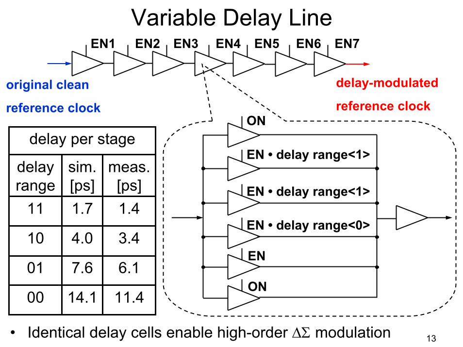
Variable Delay LineEN1 EN2 EN3 EN4
original clean
reference clock
delay-modulated
reference clockON
EN • delay range<0>
EN • delay range<1>
EN • delay range<1>
EN
ON
EN5 EN6 EN7
delay per stage
11.414.100
6.17.601
3.44.010
1.41.711
meas. [ps]
sim. [ps]
delay range
• Identical delay cells enable high-order ∆Σ modulation
14
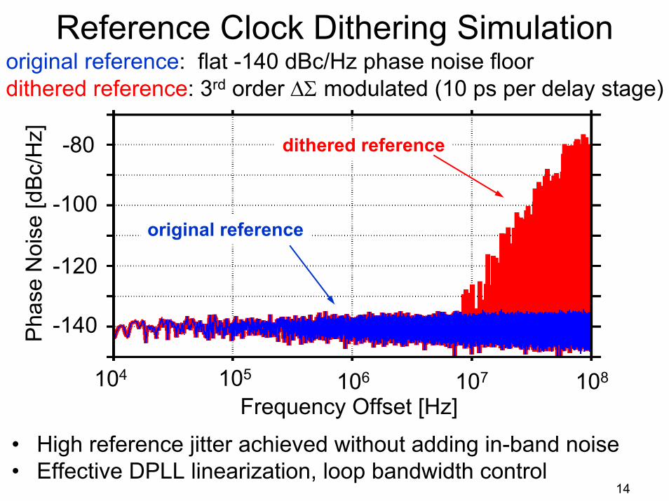
Reference Clock Dithering Simulationoriginal reference: flat -140 dBc/Hz phase noise floordithered reference: 3rd order ∆Σ modulated (10 ps per delay stage)
Frequency Offset [Hz]105 106 107
original reference
dithered reference
Pha
se N
oise
[dB
c/H
z]
-100
-120
-140
-80
104 108
• High reference jitter achieved without adding in-band noise• Effective DPLL linearization, loop bandwidth control

15
-70
-150
Frequency Offset [Hz]103 104 105 106 107 108 109 1010
-80
-90-100-110
-120-130
-140
with reference dithering
σ = 137 fs
no reference dithering
σ = 140 fs
• DPLL bandwidth control by proportional path gain or by reference dithering • Reference dithering does not degrade the RMS jitter σ (6.5 MHz to 5.5 GHz)
VDDA=1.2V (17mA), VDD=1.1V (9.2mA), N = 40 (275 MHz reference)Measured 11 GHz Phase Noise Plots
Pha
se N
oise
[dB
c/H
z]

16
11 GHz BB-DPLL Die Photograph
Digital Core
CMOS PrescalerOutput Driver
LC-DCO
pad pitch: 100 µm
• DPLL area can be improved with more efficient layout

17
BB-DPLL Performance Summary
-121 dBc/Hz
345 fs 3
138 fs 1,2
8.1 – 11.8 GHz31 mW
1.2 V, 17 mA1.1 V, 9.1 mA
410 µm × 215 µm65 nm bulk
11 GHz 20 GHz
-112 dBc/HzPhase Noise (at 10 MHz offset)
962 fsRMS Jitter ( 1MHz – 10 GHz )
190 fsRMS Jitter ( fc/1167 – fc/2 )16.4 – 22.4 GHzTuning Range
64 mWTotal Power Dissipation1.6 V, 37 mADCO, Prescalers1.1 V, 4.5 mADigital CoreVoltages,
Currents
425 µm × 265 µmAreaCMOS Technology
1 RMS jitter (6.5 MHz to 5.5 GHz) measured at 14 points across the 10.64 GHz to 11.16 GHz band (in 1 MHz reference steps) was under 178 fs.2 at T = 125°C, 8.4 GHz the RMS jitter (5 MHz to 4.2 GHz) was 205 fs.3 n-cycle jitter under 0.8 ps RMS (from 1-cycle to 1024-cycle; oscilloscope noise floor ~ 450 fs )

18
Conclusion
• Integer-N BB-DPLLs at 11 GHz and 20 GHz meet integrated jitter and bandwidth requirements of high-speed serial communication applications.
• Key design features: – low-gain low-latency proportional path control is
directly applied to the DCO– two different implementation types of DCO
proportional controls demonstrated.• Time-domain reference dithering technique with noise
shaping to effectively control BB-DPLL bandwidth demonstrated.