baseband module (bbm) specification version 1 - · pdf fileissue 1.0 1 (27) open base station...
TRANSCRIPT
Issue 1.0 1 (27)
OPEN BASE STATION ARCHITECTURE INITIATIVEBaseband Module (BBM) Specification
Version 1.0

OPEN BASE STATION ARCHITECTURE INITIATIVE
Issue 1.0 2 (27)
Preface1
OBSAI Specification documents are developed within the Technical Working Groups 2of the Open Base Station Architecture Initiative Special Interest Group (OBSAI SIG). 3Members of the OBSAI TWG serve voluntarily and without compensation. The 4specifications developed within OBSAI represent a consensus of the broad expertise 5on the subject within the OBSAI SIG.6
Use of an OBSAI Specification is wholly voluntary. The existence of an OBSAI 7Specification does not imply that there are no other ways to produce, test, measure, 8purchase, market, or provide other goods and services related to the scope of the 9OBSAI Specification. Furthermore, the viewpoint expressed at the time a 10specification is approved and issued is subject to change brought about through 11developments in the state of the art and comments received from users of the 12specification. Every OBSAI Specification is subjected to review in accordance with 13the Open Base Station Architecture Initiative Rules And Procedures.14
Implementation of all or part of an OBSAI Specification may require licenses under 15third party intellectual property rights, including without limitation, patent rights (such a 16third party may or may not be an OBSAI Member). The Promoters of the OBSAI 17Specification are not responsible and shall not be held responsible in any manner for 18identifying or failing to identify any or all such third party intellectual property rights.19
The information in this document is subject to change without notice and describes 20only the product defined in the introduction of this documentation. This document is 21intended for the use of OBSAI Member’s customers only for the purposes of the 22agreement under which the document is submitted, and no part of it may be 23reproduced or transmitted in any form or means without the prior written permission of 24OBSAI Management Board. The document has been prepared to be used by 25professional and properly trained personnel, and the customer assumes full 26responsibility when using it. OBSAI Management Board, Marketing Working Group 27and Technical Working Group welcome customer comments as part of the process of 28continuous development and improvement of the documentation. 29
The information or statements given in this document concerning the suitability, 30capacity, or performance of the mentioned hardware or software products cannot be 31considered binding but shall be defined in the agreement made between OBSAI 32members. However, the OBSAI Management Board, Marketing Working Group or 33Technical Working Group have made all reasonable efforts to ensure that the 34instructions contained in the document are adequate and free of material errors and 35omissions. 36
OBSAI liability for any errors in the document is limited to the documentary correction 37of errors. OBSAI WILL NOT BE RESPONSIBLE IN ANY EVENT FOR ERRORS IN 38THIS DOCUMENT OR FOR ANY DAMAGES, INCIDENTAL OR CONSEQUENTIAL 39(INCLUDING MONETARY LOSSES), that might arise from the use of this document 40or the information in it.41
This document and the product it describes are considered protected by copyright 42according to the applicable laws.43
OBSAI logo is a registered trademark of Open Base Station Architecture Initiative 44Special Interest Group. 45
46
OPEN BASE STATION ARCHITECTURE INITIATIVE
Issue 1.0 3 (27)
Other product names mentioned in this document may be trademarks of their 1respective companies, and they are mentioned for identification purposes only.2
Copyright © Open Base Station Architecture Initiative Special Interest Group. All rights 3reserved.4
Users are cautioned to check to determine that they have the latest edition of any 5OBSAI Specification. 6
Interpretations: Occasionally questions may arise regarding the meaning of portions of 7standards as they relate to specific applications. When the need for interpretations is 8brought to the attention of OBSAI, the OBSAI TWG will initiate action to prepare 9appropriate responses. Since OBSAI Specifications represent a consensus of OBSAI 10Member’s interests, it is important to ensure that any interpretation has also received 11the concurrence of a balance of interests. For this reason OBSAI and the members of 12its Technical Working Groups are not able to provide an instant response to 13interpretation requests except in those cases where the matter has previously 14received formal consideration. 15
Comments on specifications and requests for interpretations should be addressed to:16
Peter Kenington17
Chairman, OBSAI Technical Working Group18
Linear Communications Consultants Ltd.19
Email: [email protected]

OPEN BASE STATION ARCHITECTURE INITIATIVE
Issue 1.0 4 (27)
Contents
1 Summary of changes.........................................................................................72 Scope ..................................................................................................................83 General................................................................................................................9
3.1 Topology and Dimensioning Requirements ..................................................93.2 Hot Insertion and Removal..........................................................................103.3 Signal Naming Conventions........................................................................113.4 Connector Naming and Orientation.............................................................13
4 BBM Interfaces .................................................................................................154.1 Signal List ...................................................................................................154.2 Signal Specification.....................................................................................17
4.2.1 Common Signals..................................................................................174.2.2 BBM Specific Signals...........................................................................194.2.3 BBM Unspecified Signals.....................................................................21
5 BBM Pin Assignments .....................................................................................225.1 J1 Data Connector ......................................................................................225.2 J2 Data Connector (Optional)......................................................................235.3 Power Connector ........................................................................................24
6 Glossary............................................................................................................256.1 Abbreviations ..............................................................................................256.2 Definition of Terms ......................................................................................25
7 References........................................................................................................277.1 OBSAI .........................................................................................................277.2 IEEE............................................................................................................277.3 ANSI............................................................................................................27
OPEN BASE STATION ARCHITECTURE INITIATIVE
Issue 1.0 5 (27)
Figures
Figure 2-1 BTS Reference Architecture.......................................................................8
Figure 3-1 Signal Direction Definition ........................................................................12
Figure 3-2 Connector Positions and Naming (module rear view) ..............................14
Figure 4-1 TIN_SYNC Timing.........................................................................................19

OPEN BASE STATION ARCHITECTURE INITIATIVE
Issue 1.0 6 (27)
List of Tables
Table 3-1 BBM Signal Abbreviations.........................................................................11
Table 4-1 BBM Interface signal list............................................................................16
Table 4-3 System Clock Electrical Parameters .........................................................18
Table 4-4 Synchronization Signal Electrical and Timing Parameters ........................20
Table 5-1 Data Connector J1 Pin Assignment...........................................................22
Table 5-2 Data Connector J2 Pin Assignment...........................................................23
Table 5-3 Power Connector P1 Pin Assignment .......................................................24
Table 5-4 Power Connector P2 Pin Assignment .......................................................24
OPEN BASE STATION ARCHITECTURE INITIATIVE
Issue 1.0 7 (27)
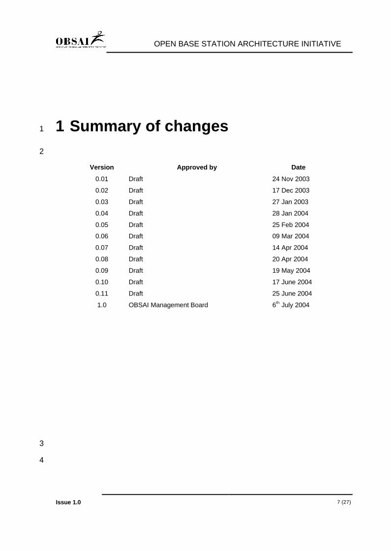
1 Summary of changes1
2
Version Approved by Date
0.01 Draft 24 Nov 2003
0.02 Draft 17 Dec 2003
0.03 Draft 27 Jan 2003
0.04 Draft 28 Jan 2004
0.05 Draft 25 Feb 2004
0.06 Draft 09 Mar 2004
0.07 Draft 14 Apr 2004
0.08 Draft 20 Apr 2004
0.09 Draft 19 May 2004
0.10 Draft 17 June 2004
0.11 Draft 25 June 2004
1.0 OBSAI Management Board 6th July 2004
3
4
OPEN BASE STATION ARCHITECTURE INITIATIVE
Issue 1.0 8 (27)
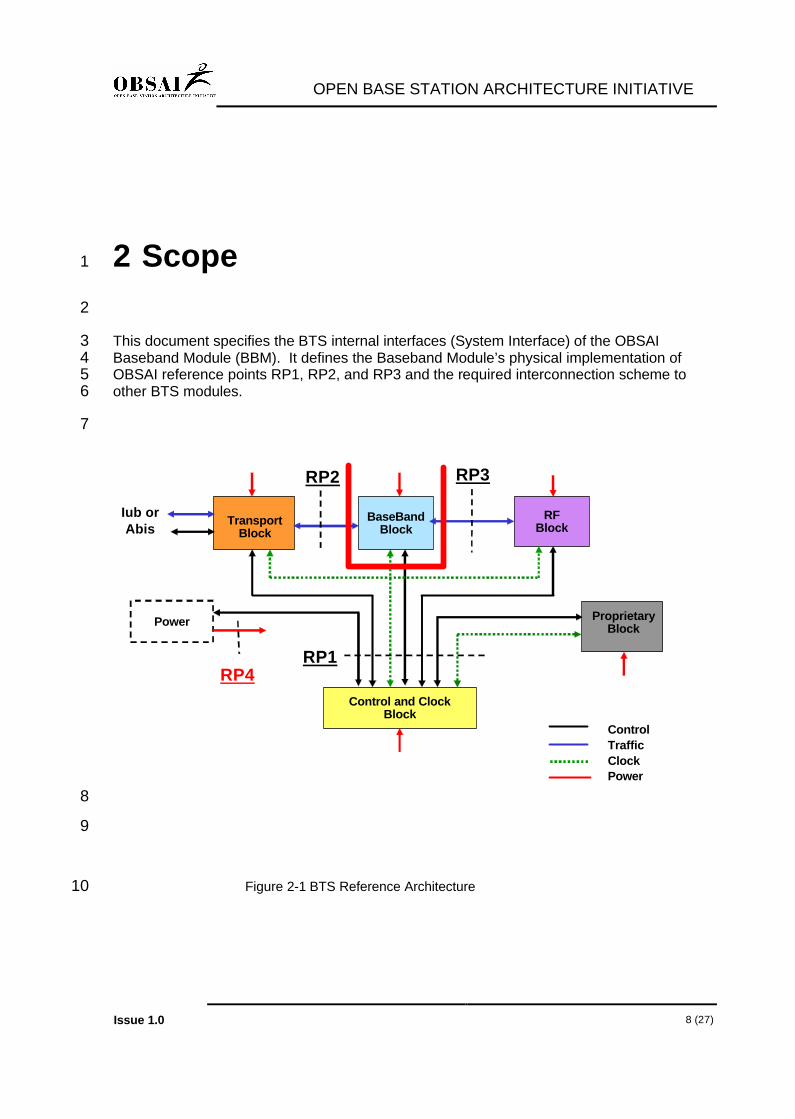
2 Scope 1
2
This document specifies the BTS internal interfaces (System Interface) of the OBSAI 3Baseband Module (BBM). It defines the Baseband Module’s physical implementation of 4OBSAI reference points RP1, RP2, and RP3 and the required interconnection scheme to 5other BTS modules.6
7
TransportBlock
Control and ClockBlock
BaseBandBlock
RFBlock
RP1
RP2 RP3
Iub orAbis
ProprietaryBlockPower
RP4
ControlTrafficClockPower
8
9
Figure 2-1 BTS Reference Architecture10
OPEN BASE STATION ARCHITECTURE INITIATIVE
Issue 1.0 9 (27)
3 General1
This module interface specification focuses on the physical interface requirements of 2the BBM. The actual BTS and BBM designs are out of the scope of this document. 3Guidelines for implementation are given where appropriate.4
3.1 Topology and Dimensioning Requirements5
The BTS internal interface provided by the BBM supports the following functions:6
� Control and Management Plane message transfer to and from the Control 7and Clock Modules (CCMs) via RP18
� User Plane data transfer to and from the Transport Modules (TMs) via RP29
� Baseband data transfer to and from the Radio Frequency Modules (RFMs) 10via RP311
All Control and Management Plane data, as well as all User Plane data is transferred 12to the BBM via a single, optionally redundant, Ethernet network. The BBM shall 13contain two Ethernet fabric ports for connection to this network. The first fabric port 14connects the BBM to the primary Ethernet network. The second fabric port connects 15the BBM to the secondary (redundant) Ethernet network, if one is present in the 16system. 17
The fabric ports shall be implemented as Ethernet type 100Base-TX or 1000Base-T. 18The 1000Base-T option allows for high capacity BBMs that may need higher 19throughput than 100Base-T can provide. In either case, both Ethernet interfaces on 20the BBM shall be of the same type.21
The OBSAI architecture supports different system configurations, and along with that, 22different numbers of BBMs and RFMs per system. Each BBM shall have up to 9 23pairs of unidirectional links with differential signaling toward the RP3 interface. See 24the RP3 Reference Point Specification [OBSAI RP3] for detailed dimensioning 25information.26
BBM redundancy is optionally supported by an N+1 redundancy scheme.27
28
OPEN BASE STATION ARCHITECTURE INITIATIVE
Issue 1.0 10 (27)
3.2 Hot Insertion and Removal1
All signals shall support hot insertion and removal. Hot insertion is supported on the 2module by delayed (insertion) and early (removal) switch on/off of the power supply,3by means of a last mating enable pin at the power connector. Every source and sink 4of a signal shall survive without any damage, if the connected signal is within its 5specified operating range.6
7

OPEN BASE STATION ARCHITECTURE INITIATIVE
Issue 1.0 11 (27)
3.3 Signal Naming Conventions1
All signal names start with a 2-5-letter abbreviation that describes the general 2function of the signal group. 3
4
Abbreviation Full Name Comment
MA Module Address -
SA Shelf Address -
MNC Module Not Connected Not Connected on Module
FP Fabric Port -
SCLK System Clock -
SYNC Synchronization Signal
RP3L Reference Point 3 Link -
BBMUS BBM Unspecified -
GND Ground Digital Ground
BPNC Backplane Not Connected Not Connected on Backplane
Table 3-1 BBM Signal Abbreviations5
The signal name abbreviation is followed by a numerical index to distinguish between 6several instances of a signal inside a signal group. The index starts with the value 7“0”.8
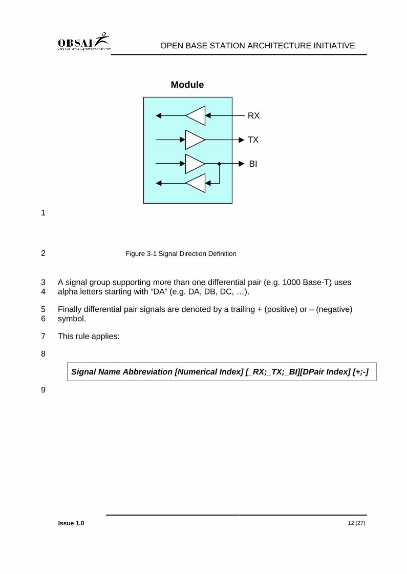
Additionally a direction indication is attached for signal groups with receive (_RX), 9transmit (_TX) or bidirectional (_BI) signals, if there is a need to distinguish between 10them. The direction is derived from the physical characteristics at the module 11boundary. The direction of signals not explicitly indicated by the signal name is 12specified in the signal list (section 4.1), or left unspecified intentionally.13
OPEN BASE STATION ARCHITECTURE INITIATIVE
Issue 1.0 12 (27)
Module
RX
TX
BI
1
Figure 3-1 Signal Direction Definition2
A signal group supporting more than one differential pair (e.g. 1000 Base-T) uses 3alpha letters starting with “DA” (e.g. DA, DB, DC, …).4
Finally differential pair signals are denoted by a trailing + (positive) or – (negative) 5symbol.6
This rule applies:7
8
Signal Name Abbreviation [Numerical Index] [_RX;_TX;_BI][DPair Index] [+;-]
9
OPEN BASE STATION ARCHITECTURE INITIATIVE
Issue 1.0 13 (27)
3.4 Connector Naming and Orientation1
Definitions:2
� Female connectors use the reference designator prefix J3
� Male connectors use the reference designator prefix P4
� Mechanical guiding pins use the reference designator prefix G5
� Mechanical guiding holes use the reference designator prefix H6
A numerical index follows the designator prefix. 7
The following rule applies to the module:8
9
Prefix [Module Index]
10
This concept also applies to the backplane connectors. Although this is not included 11within the scope of this specification, it is nevertheless recommended that users12follow this guidance. In addition to the module index the backplane has a slot index, 13which references the slot position.14
The following rule applies to the backplane:15
16
Prefix [Module Index] [Slot Index]
17
Figure 3-2 shows the module connector naming.18

OPEN BASE STATION ARCHITECTURE INITIATIVE
Issue 1.0 14 (27)
1
Figure 3-2 Connector Positions and Naming (module rear view)2
3
1
1
1
1
Data Connector J2(without guide)
Data Connector J1(with guide)
Power Connector P1
Optional Power Connector P2
J1
J2
P1
P2
PC
B
1 2
OPEN BASE STATION ARCHITECTURE INITIATIVE
Issue 1.0 15 (27)
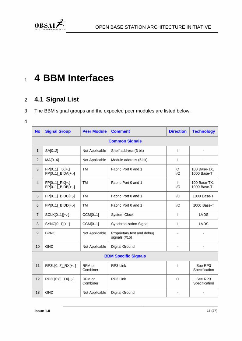
4 BBM Interfaces1
4.1 Signal List2
The BBM signal groups and the expected peer modules are listed below:3
4
No Signal Group Peer Module Comment Direction Technology
Common Signals
1 SA[0..2] Not Applicable Shelf address (3 bit) I -
2 MA[0..4] Not Applicable Module address (5 bit) I -
3 FP[0..1]_TX[+,]FP[0..1]_BIDA[+,-]
TM Fabric Port 0 and 1 OI/O
100 Base-TX,1000 Base-T
4 FP[0..1]_RX[+,]FP[0..1]_BIDB[+,-]
TM Fabric Port 0 and 1 II/O
100 Base-TX,1000 Base-T
5 FP[0..1]_BIDC[+,-] TM Fabric Port 0 and 1 I/O 1000 Base-T,
6 FP[0..1]_BIDD[+,-] TM Fabric Port 0 and 1 I/O 1000 Base-T
7 SCLK[0..1][+,-] CCM[0..1] System Clock I LVDS
8 SYNC[0..1][+,-] CCM[0..1] Synchronization Signal I LVDS
9 BPNC Not Applicable Proprietary test and debug signals (#15)
- -
10 GND Not Applicable Digital Ground - -
BBM Specific Signals
11 RP3L[0..8]_RX[+,-] RFM or Combiner
RP3 Link I See RP3 Specification
12 RP3L[0:8]_TX[+,-] RFM or Combiner
RP3 Link O See RP3 Specification
13 GND Not Applicable Digital Ground - -

OPEN BASE STATION ARCHITECTURE INITIATIVE
Issue 1.0 16 (27)
BBM Unspecified Signals
14 BBMUS Not Applicable Proprietary Signals - -
BBM Power Signals
15 PWR_POS Not Applicable Supply Positive - Power
16 PWR_NEG Not Applicable Supply Negative - Power
17 PWR_EN Not Applicable Power Enable I -
18 GND Not Applicable Digital Ground - -
Table 4-1 BBM Interface signal list12
OPEN BASE STATION ARCHITECTURE INITIATIVE
Issue 1.0 17 (27)
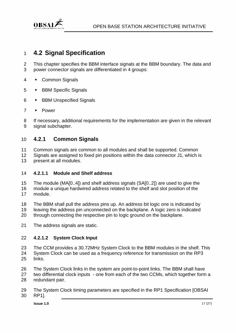
4.2 Signal Specification1
This chapter specifies the BBM interface signals at the BBM boundary. The data and 2power connector signals are differentiated in 4 groups:3
� Common Signals4
� BBM Specific Signals5
� BBM Unspecified Signals6
� Power7
If necessary, additional requirements for the implementation are given in the relevant8signal subchapter.9
4.2.1 Common Signals10
Common signals are common to all modules and shall be supported. Common 11Signals are assigned to fixed pin positions within the data connector J1, which is 12present at all modules.13
4.2.1.1 Module and Shelf address14
The module (MA[0..4]) and shelf address signals (SA[0..2]) are used to give the 15module a unique hardwired address related to the shelf and slot position of the 16module. 17
The BBM shall pull the address pins up. An address bit logic one is indicated by 18leaving the address pin unconnected on the backplane. A logic zero is indicated 19through connecting the respective pin to logic ground on the backplane.20
The address signals are static.21
4.2.1.2 System Clock Input22
The CCM provides a 30.72MHz System Clock to the BBM modules in the shelf. This 23System Clock can be used as a frequency reference for transmission on the RP3 24links.25
The System Clock links in the system are point-to-point links. The BBM shall have 26two differential clock inputs - one from each of the two CCMs, which together form a 27redundant pair.28
The System Clock timing parameters are specified in the RP1 Specification [OBSAI 29RP1].30
OPEN BASE STATION ARCHITECTURE INITIATIVE
Issue 1.0 18 (27)
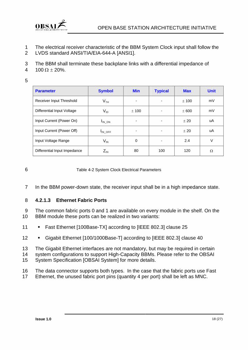
The electrical receiver characteristic of the BBM System Clock input shall follow the 1LVDS standard ANSI/TIA/EIA-644-A [ANSI1]. 2
The BBM shall terminate these backplane links with a differential impedance of 3100 � � 20%.4
5
Parameter Symbol Min Typical Max Unit
Receiver Input Threshold VTH - - � 100 mV
Differential Input Voltage VID � 100 - � 600 mV
Input Current (Power On) IIN_ON - - � 20 uA
Input Current (Power Off) IIN_OFF - - � 20 uA
Input Voltage Range VIN 0 - 2.4 V
Differential Input Impedance ZIN 80 100 120 �
Table 4-2 System Clock Electrical Parameters6
In the BBM power-down state, the receiver input shall be in a high impedance state.7
4.2.1.3 Ethernet Fabric Ports8
The common fabric ports 0 and 1 are available on every module in the shelf. On the 9BBM module these ports can be realized in two variants:10
� Fast Ethernet [100Base-TX] according to [IEEE 802.3] clause 2511
� Gigabit Ethernet [100/1000Base-T] according to [IEEE 802.3] clause 4012
The Gigabit Ethernet interfaces are not mandatory, but may be required in certain 13system configurations to support High-Capacity BBMs. Please refer to the OBSAI 14System Specification [OBSAI System] for more details.15
The data connector supports both types. In the case that the fabric ports use Fast 16Ethernet, the unused fabric port pins (quantity 4 per port) shall be left as MNC.17
OPEN BASE STATION ARCHITECTURE INITIATIVE
Issue 1.0 19 (27)
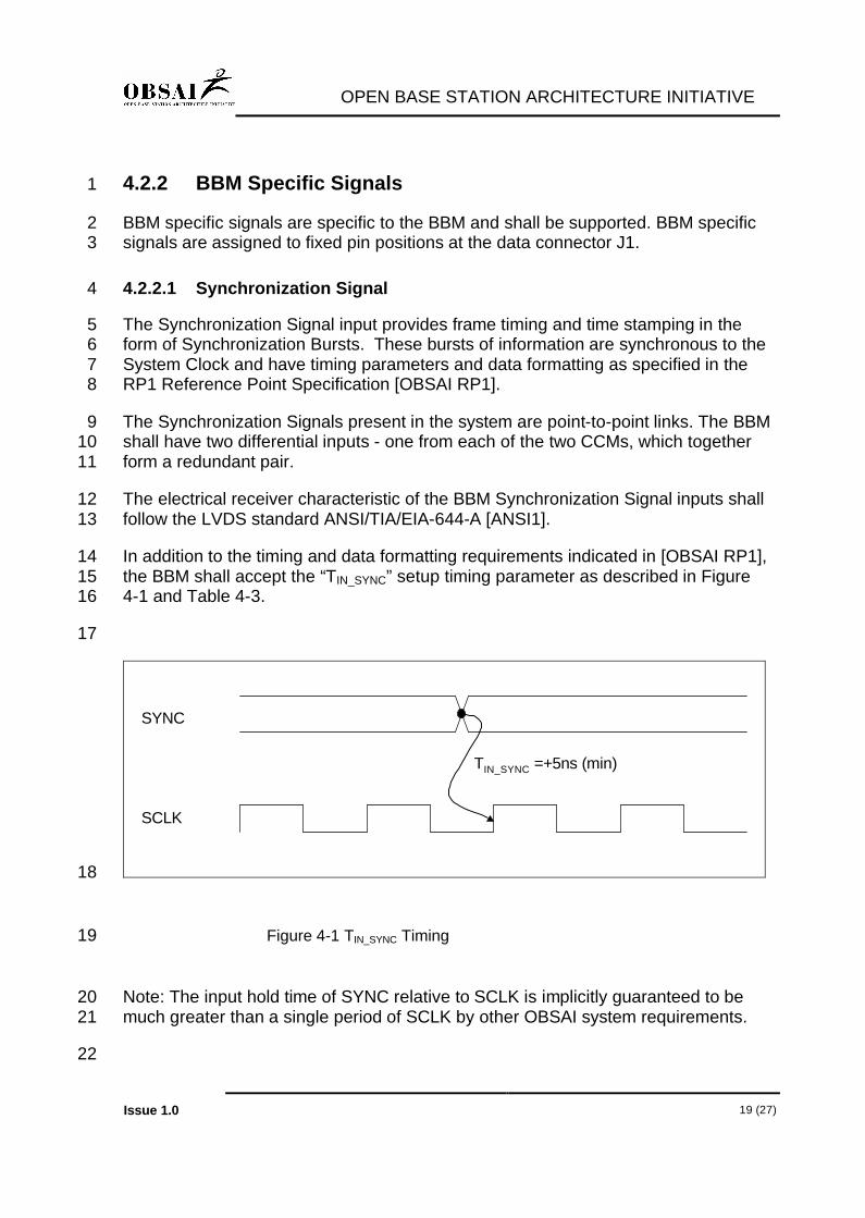
4.2.2 BBM Specific Signals1
BBM specific signals are specific to the BBM and shall be supported. BBM specific 2signals are assigned to fixed pin positions at the data connector J1.3
4.2.2.1 Synchronization Signal4
The Synchronization Signal input provides frame timing and time stamping in the 5form of Synchronization Bursts. These bursts of information are synchronous to the 6System Clock and have timing parameters and data formatting as specified in the 7RP1 Reference Point Specification [OBSAI RP1].8
The Synchronization Signals present in the system are point-to-point links. The BBM 9shall have two differential inputs - one from each of the two CCMs, which together 10form a redundant pair.11
The electrical receiver characteristic of the BBM Synchronization Signal inputs shall 12follow the LVDS standard ANSI/TIA/EIA-644-A [ANSI1]. 13
In addition to the timing and data formatting requirements indicated in [OBSAI RP1], 14the BBM shall accept the “TIN_SYNC” setup timing parameter as described in Figure154-1 and Table 4-3.16
17
SYNC
SCLK
TIN_SYNC =+5ns (min)
18
Figure 4-1 TIN_SYNC Timing19
Note: The input hold time of SYNC relative to SCLK is implicitly guaranteed to be 20much greater than a single period of SCLK by other OBSAI system requirements.21
22

OPEN BASE STATION ARCHITECTURE INITIATIVE
Issue 1.0 20 (27)
Parameter Symbol Min Typical Max Unit
Receiver Input Threshold VTH - - � 100 mV
Differential Input Voltage VID � 100 - � 600 mV
Input Current (Power On) IIN_ON - - � 20 uA
Input Current (Power Off) IIN_OFF - - � 20 uA
Input Voltage Range VIN 0 - 2.4 V
Differential Input Impedance ZIN 80 100 120 �
SYNC to SCLK Setup TIN_SYNC 5 - - ns
Table 4-3 Synchronization Signal Electrical and Timing Parameters1
The BBM shall terminate these backplane signals with 100 � � 20%.2
3
4.2.2.2 RP3 Links4
The BBM connects to RFMs or to a Combiner/Distributor unit through RP3 Links. An5RP3 Link consists of a pair of unidirectional links, one being an incoming signal, and 6the other being an outgoing signal. 7
Since different system configurations call for differing numbers of BBMs and RFMs, 8there will exist some unused RP3 Links in some system configurations. All unused 9links shall be disabled for power conservation purposes.10
In the BBM power-down state, the transmitter outputs and receiver inputs shall be in 11a high impedance state.12
Refer to the RP3 Reference Point Specification [OBSAI RP3] for other detailed 13electrical specifications of these links.14
OPEN BASE STATION ARCHITECTURE INITIATIVE
Issue 1.0 21 (27)
4.2.3 BBM Unspecified Signals1
BBM Unspecified Signals are optional. Their functional and electrical characteristics 2are not specified. If present, BBM Unspecified Signals shall be located on the data 3connector J2.4
Since they are not specified by OBSAI, connecting BBM Unspecified Signals may 5cause incompatibility with certain backplane configurations.6
7
OPEN BASE STATION ARCHITECTURE INITIATIVE
Issue 1.0 22 (27)
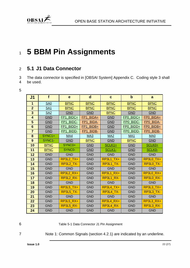
5 BBM Pin Assignments 1
5.1 J1 Data Connector2
The data connector is specified in [OBSAI System] Appendix C. Coding style 3 shall 3be used.4
5
J1 f e d c b a1 SA0 BPNC BPNC BPNC BPNC BPNC2 SA1 BPNC BPNC BPNC BPNC BPNC3 SA2 GND GND BPNC GND GND4 GND FP1_BIDC+ FP1_BIDA+ GND FP0_BIDC+ FP0_BIDA+5 GND FP1_BIDC- FP1_BIDA- GND FP0_BIDC- FP0_BIDA-6 GND FP1_BIDD+ FP1_BIDB+ GND FP0_BIDD+ FP0_BIDB+7 GND FP1_BIDD- FP1_BIDB- GND FP0_BIDD- FP0_BIDB-8 SYNC1+ MA4 MA3 MA2 MA1 MA09 SYNC1- GND BPNC GND BPNC GND
10 BPNC SYNC0+ GND SCLK1+ GND SCLK0+11 BPNC SYNC0- GND SCLK1- GND SCLK0-12 GND GND GND GND GND GND13 GND RP3L2_TX+ GND RP3L1_TX+ GND RP3L0_TX+14 GND RP3L2_TX- GND RP3L1_TX- GND RP3L0_TX-15 GND GND GND GND GND GND16 GND RP3L2_RX+ GND RP3L1_RX+ GND RP3L0_RX+17 GND RP3L2_RX- GND RP3L1_RX- GND RP3L0_RX-18 GND GND GND GND GND GND19 GND RP3L5_TX+ GND RP3L4_TX+ GND RP3L3_TX+20 GND RP3L5_TX- GND RP3L4_TX- GND RP3L3_TX-21 GND GND GND GND GND GND22 GND RP3L5_RX+ GND RP3L4_RX+ GND RP3L3_RX+23 GND RP3L5_RX- GND RP3L4_RX- GND RP3L3_RX-24 GND GND GND GND GND GND
Table 5-1 Data Connector J1 Pin Assignment6
Note 1: Common Signals (section 4.2.1) are indicated by an underline.7
OPEN BASE STATION ARCHITECTURE INITIATIVE
Issue 1.0 23 (27)
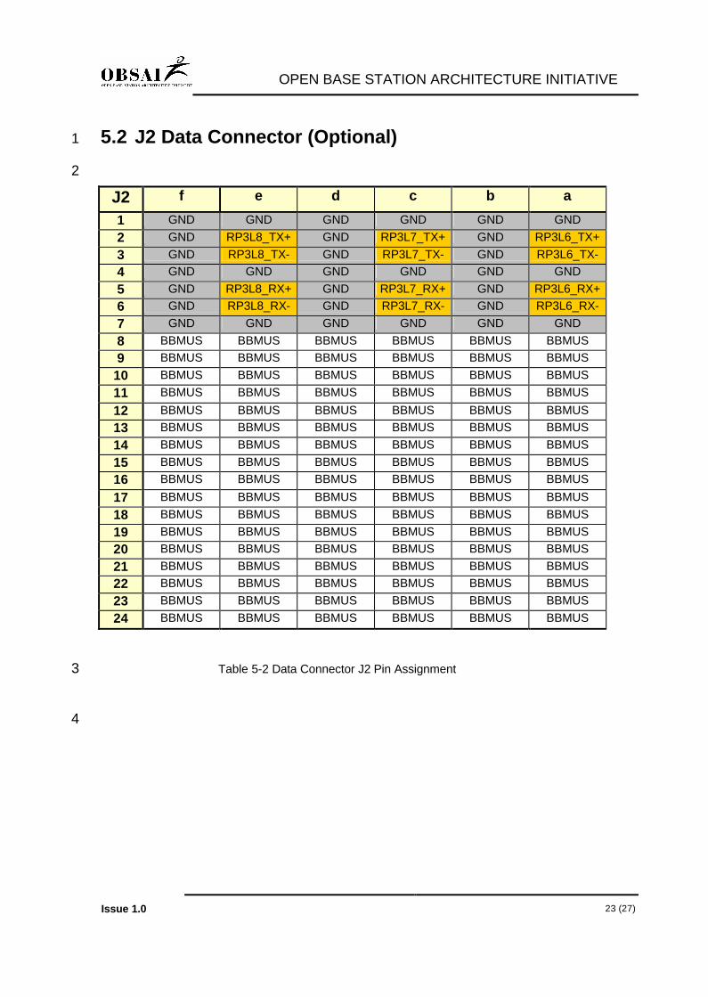
5.2 J2 Data Connector (Optional)1
2
J2 f e d c b a1 GND GND GND GND GND GND2 GND RP3L8_TX+ GND RP3L7_TX+ GND RP3L6_TX+3 GND RP3L8_TX- GND RP3L7_TX- GND RP3L6_TX-4 GND GND GND GND GND GND5 GND RP3L8_RX+ GND RP3L7_RX+ GND RP3L6_RX+6 GND RP3L8_RX- GND RP3L7_RX- GND RP3L6_RX-7 GND GND GND GND GND GND8 BBMUS BBMUS BBMUS BBMUS BBMUS BBMUS9 BBMUS BBMUS BBMUS BBMUS BBMUS BBMUS
10 BBMUS BBMUS BBMUS BBMUS BBMUS BBMUS11 BBMUS BBMUS BBMUS BBMUS BBMUS BBMUS12 BBMUS BBMUS BBMUS BBMUS BBMUS BBMUS13 BBMUS BBMUS BBMUS BBMUS BBMUS BBMUS14 BBMUS BBMUS BBMUS BBMUS BBMUS BBMUS15 BBMUS BBMUS BBMUS BBMUS BBMUS BBMUS16 BBMUS BBMUS BBMUS BBMUS BBMUS BBMUS17 BBMUS BBMUS BBMUS BBMUS BBMUS BBMUS18 BBMUS BBMUS BBMUS BBMUS BBMUS BBMUS19 BBMUS BBMUS BBMUS BBMUS BBMUS BBMUS20 BBMUS BBMUS BBMUS BBMUS BBMUS BBMUS21 BBMUS BBMUS BBMUS BBMUS BBMUS BBMUS22 BBMUS BBMUS BBMUS BBMUS BBMUS BBMUS23 BBMUS BBMUS BBMUS BBMUS BBMUS BBMUS24 BBMUS BBMUS BBMUS BBMUS BBMUS BBMUS
Table 5-2 Data Connector J2 Pin Assignment3
4

OPEN BASE STATION ARCHITECTURE INITIATIVE
Issue 1.0 24 (27)
5.3 Power Connector1
BBM modules shall be equipped with a power connector P1 (OBSAI Sequenced), as 2specified in Table 5-3.3
4
P1 Signal1 PWR_POS2 PWR_ENA3 PWR_NEG4 GND
Table 5-3 Power Connector P1 Pin Assignment5
For additional supply current, the BBM may optionally be equipped with a second 6power connector P2 (OBSAI Sequenced or OBSAI Non-sequenced), as specified in 7Table 5-4.8
9
P2 Signal1 PWR_POS2 PWR_POS1
3 PWR_NEG4 PWR_NEG1
Table 5-4 Power Connector P2 Pin Assignment10
Note 1: Pins 2 and 4 can only be used with the OBSAI Non-sequenced connector.11
12
13

OPEN BASE STATION ARCHITECTURE INITIATIVE
Issue 1.0 25 (27)
6 Glossary1
6.1 Abbreviations2
For the purposes of the present document, the following abbreviations 3apply:4
ABBREVIATION DESIGNATION
BBM Base Band Module
BTS Base Transceiver Station
CCM Clock and Control Module
ESD Electrostatic Discharge
GND Ground
LVDS Low Voltage Differential Signaling
OBSAI Open Base Station Architecture Initiative
RFM Radio Frequency Module
RP1 Reference Point 1
RP2 Reference Point 2
RP3 Reference Point 3
TM Transport Module
6.2 Definition of Terms5
For the purposes of the present document, the following terms and 6definitions apply:7
Common Signals: Common Signals are common to all modules and 8shall be supported. Common Signals are assigned to fixed pin positions 9within the Data Connector(s) which are present at all modules.10
Module Type Specific Signals: Module Type Specific Signals are 11specific to a certain module types (TM, CCM, BBM, RFM, PM) and shall 12be supported. Module Type specific Signals shall be assigned to fixed 13pin positions within the Data Connector(s).14
OPEN BASE STATION ARCHITECTURE INITIATIVE
Issue 1.0 26 (27)
Module Type Unspecified Signals: Module Type Unspecified Signals 1are optional. Their functional and electrical characteristics are not 2specified. If present, Module Type Unspecified Signals shall be 3assigned to a range of pin positions within the Data Connector(s). The 4range of pin positions shall be fixed for a certain module type, but may 5differ between module types.6
Signal Group: A group of signals forming a functional entity e.g. a 7fabric port.8

OPEN BASE STATION ARCHITECTURE INITIATIVE
Issue 1.0 27 (27)
7 References1
7.1 OBSAI2
[OBSAI System] OBSAI System Reference Document V1.03
[OBSAI RP1] OBSAI Reference Point 1 Specification V1.14
[OBSAI RP2] OBSAI Reference Point 2 Specification V0.915
[OBSAI RP3] OBSAI Reference Point 3 Specification V1.06
7
8
7.2 IEEE9
[IEEE 802.3] IEEE Std, 802.3, Local and Metropolitan Area 10Networks, 2002.11
7.3 ANSI12
[ANSI] ANSI/TIA/EIA-644-A, Electrical Characteristics of 13Low Voltage Differential Signaling (LVDS) Interface 14Circuits.15
16