basicfabricationsteps andlayout - sharif
TRANSCRIPT
Basic Fabrication Stepsand Layoutand Layout
Somayyeh KoohiDepartment of Computer Engineering
Sharif University of TechnologyAdapted with modifications from lecture notes prepared by
author
Outline
� Fabrication steps� Transistor structures� Transistor behavior
Modern VLSI Design: Chap2 2 of 35Sharif University of Technology
� Transistor behavior�NMOS�PMOS
� Latch up
Foundry & Fab
� Foundry : fabrication line for hire�Foundries are major sources of fab capacity today
� Fab : Design and fabricate
Modern VLSI Design: Chap2 3 of 35Sharif University of Technology
� Fab : Design and fabricate
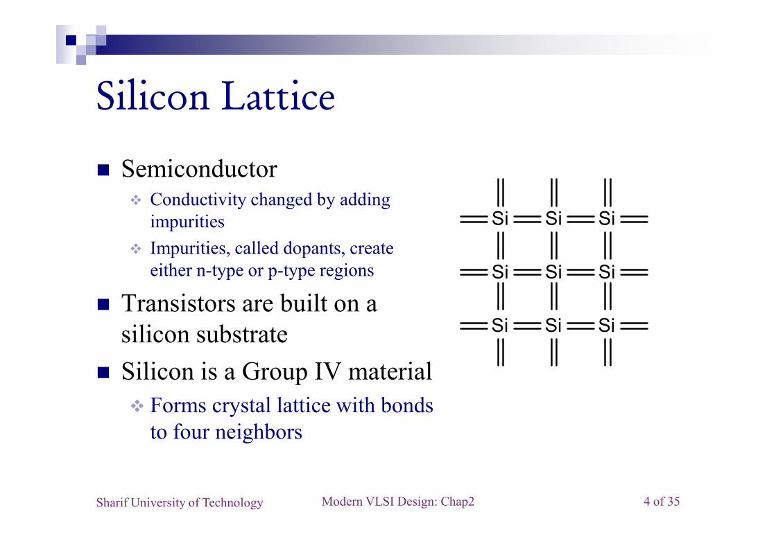
Silicon Lattice
� Semiconductor� Conductivity changed by adding
impurities� Impurities, called dopants, create
either n-type or p-type regions Si SiSi
Si SiSi
Modern VLSI Design: Chap2 4 of 35Sharif University of Technology
either n type or p type regions
� Transistors are built on asilicon substrate
� Silicon is a Group IV material� Forms crystal lattice with bonds
to four neighbors
Si SiSi
Si SiSi
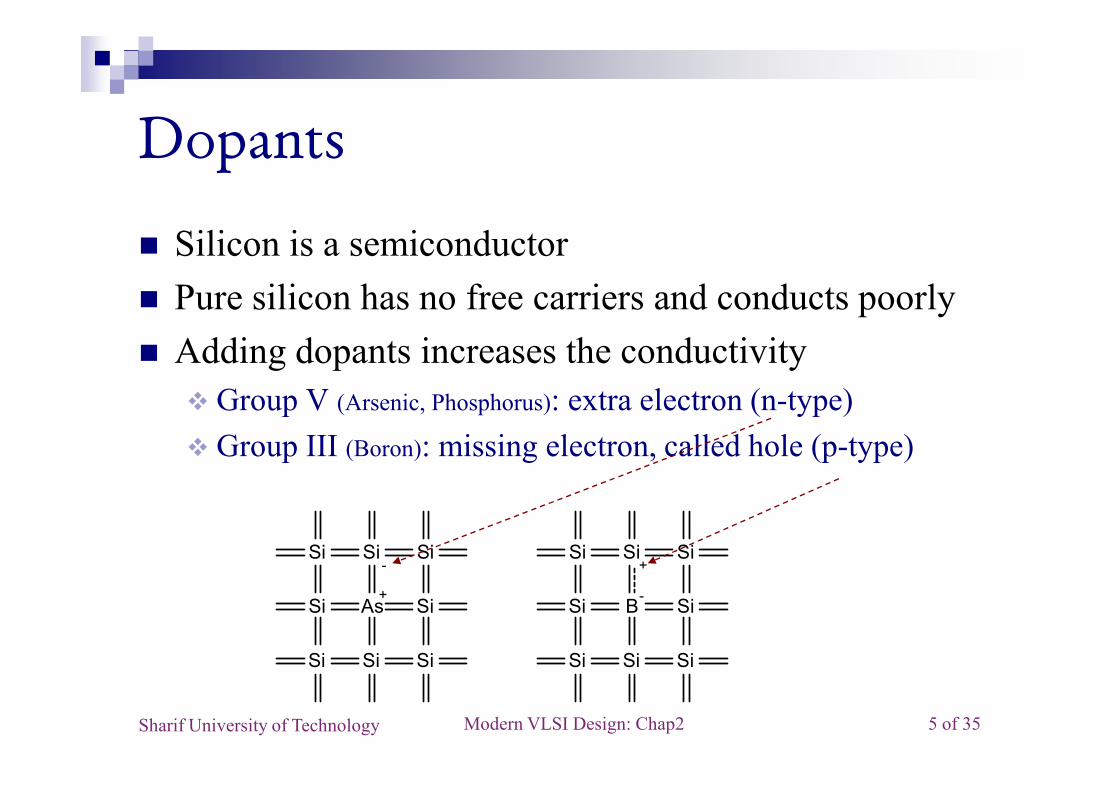
Dopants
� Silicon is a semiconductor� Pure silicon has no free carriers and conducts poorly� Adding dopants increases the conductivity
� Gro p V (A i Ph h ): e tra electron (n t pe)
Modern VLSI Design: Chap2 5 of 35Sharif University of Technology
� Group V (Arsenic, Phosphorus): extra electron (n-type)� Group III (Boron): missing electron, called hole (p-type)
As SiSi
Si SiSi
Si SiSi
B SiSi
Si SiSi
Si SiSi
-
+
+
-
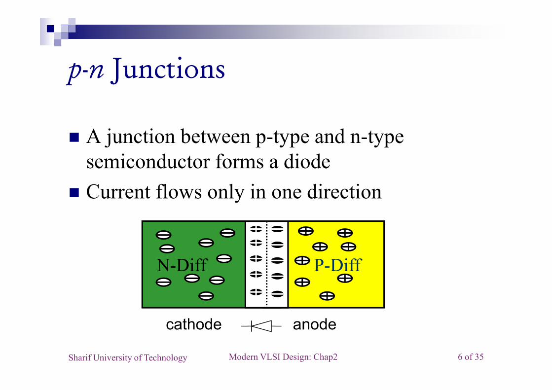
p-n Junctions
� A junction between p-type and n-typesemiconductor forms a diode
� Current flows only in one direction
Modern VLSI Design: Chap2 6 of 35Sharif University of Technology
� Current flows only in one direction
N-Diff P-Diff
anodecathode
Fabrication processes
� IC built on silicon substrate:� some structures diffused into substrate� other structures built on top of substrate
Modern VLSI Design: Chap2 7 of 35Sharif University of Technology
� Substrate regions are doped with n-type and p-typeimpurities� (n+ = heavily doped)
� Wires made of polycrystalline silicon (poly), multiplelayers of aluminum (metal)
� Silicon dioxide (SiO2) is insulator

Simple cross section
SiO2
metal2
metal3
Modern VLSI Design: Chap2 8 of 35Sharif University of Technology
substraten+ n+p+
substrate
metal1
poly
transistor via
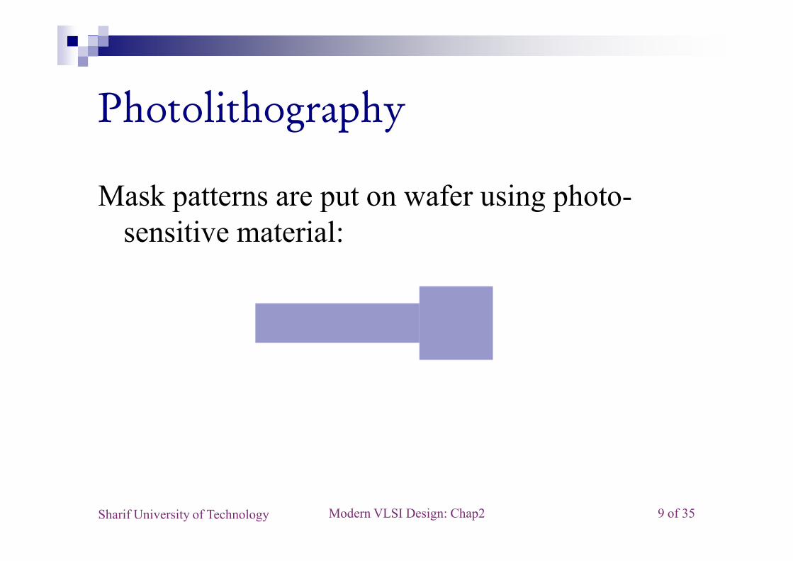
Photolithography
Mask patterns are put on wafer using photo-sensitive material:
Modern VLSI Design: Chap2 9 of 35Sharif University of Technology
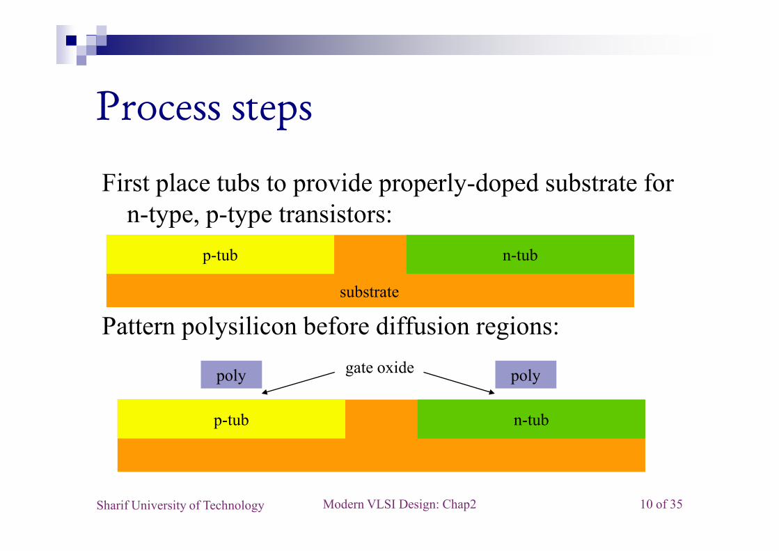
Process steps
First place tubs to provide properly-doped substrate forn-type, p-type transistors:
p-tub n-tub
Modern VLSI Design: Chap2 10 of 35Sharif University of Technology
Pattern polysilicon before diffusion regions:substrate
p-tub n-tub
poly polygate oxide
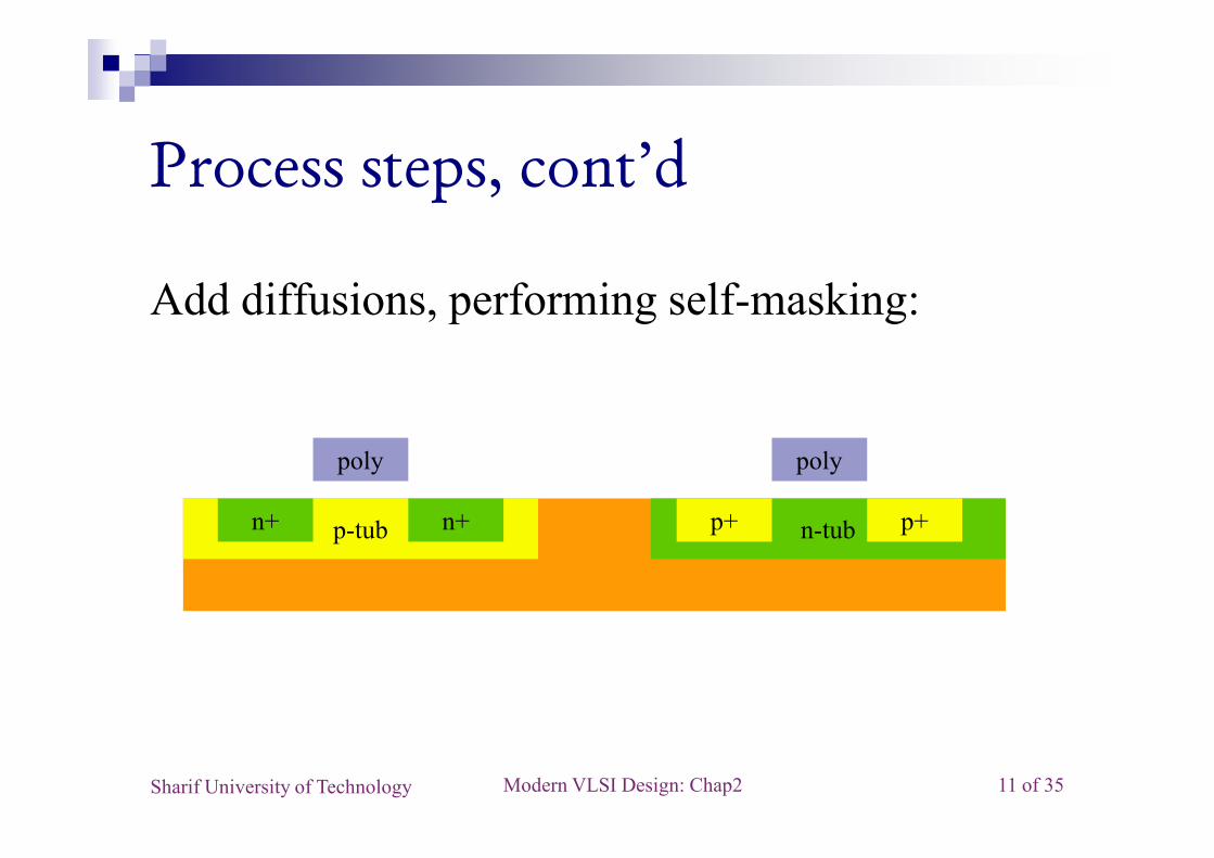
Process steps, cont’d
Add diffusions, performing self-masking:
Modern VLSI Design: Chap2 11 of 35Sharif University of Technology
p-tub n-tub
poly poly
n+n+ p+ p+
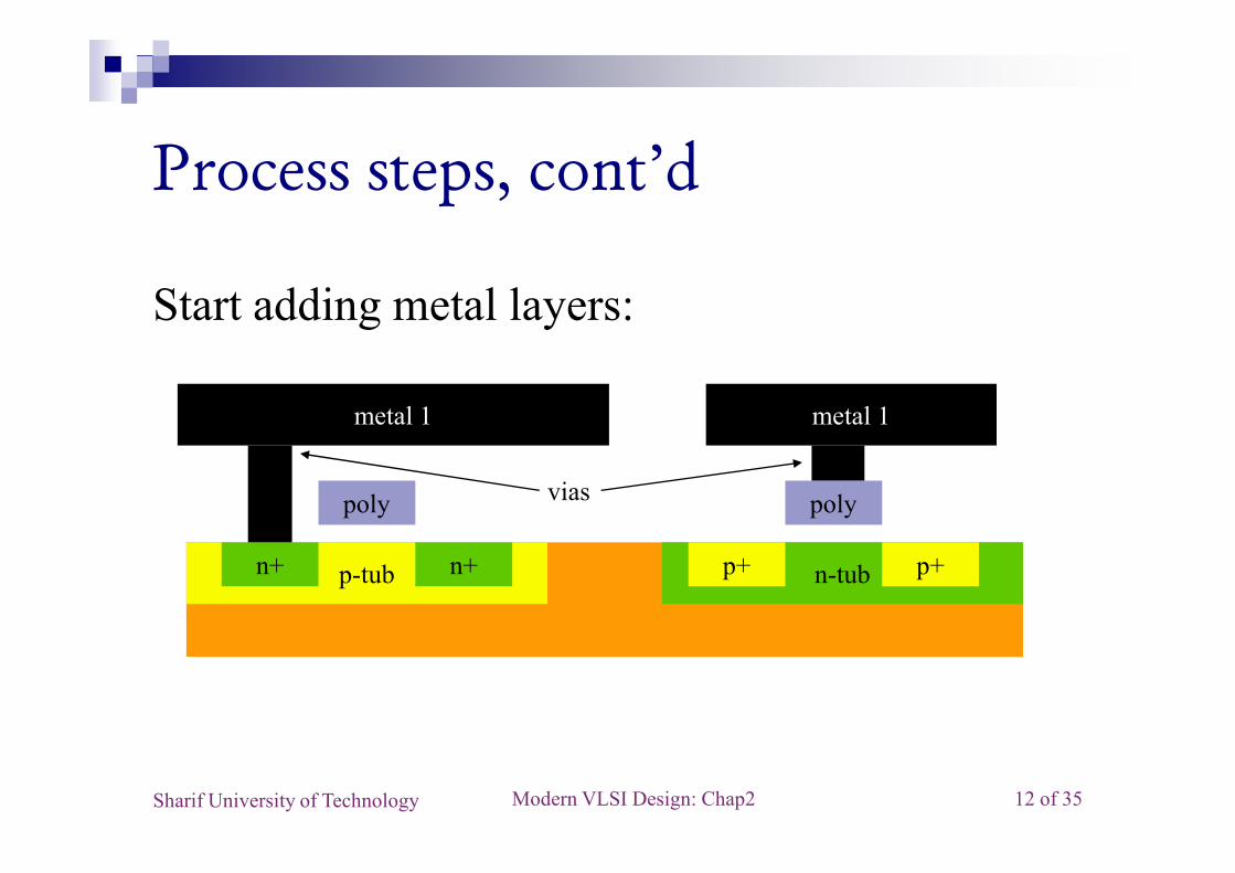
Process steps, cont’d
Start adding metal layers:
metal 1 metal 1
Modern VLSI Design: Chap2 12 of 35Sharif University of Technology
p-tub n-tub
poly poly
n+n+ p+ p+
vias
Outline
� Fabrication steps� Transistor structures� Transistor behavior
Modern VLSI Design: Chap2 13 of 35Sharif University of Technology
� Transistor behavior�NMOS�PMOS
� Latch up
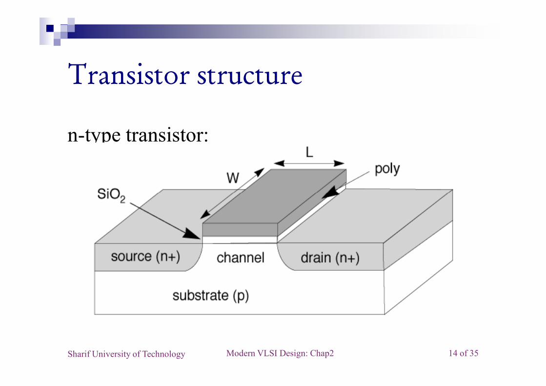
Transistor structure
n-type transistor:
Modern VLSI Design: Chap2 14 of 35Sharif University of Technology
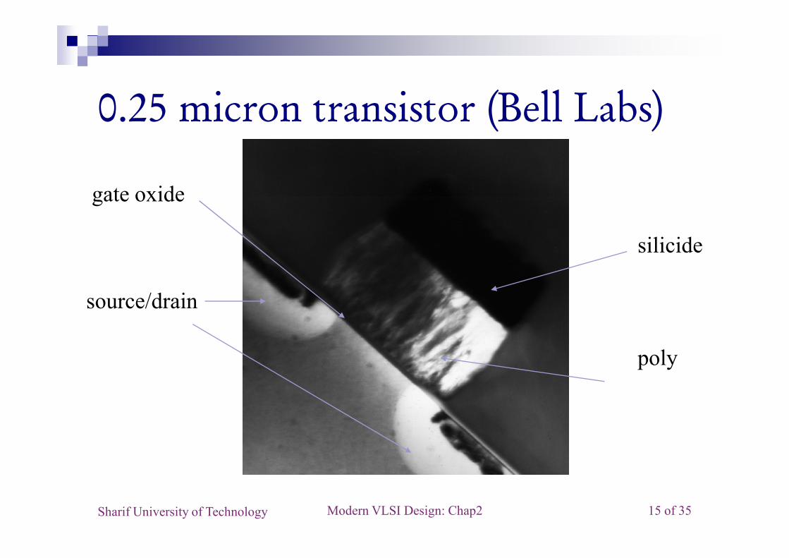
0.25 micron transistor (Bell Labs)
silicide
gate oxide
Modern VLSI Design: Chap2 15 of 35Sharif University of Technology
poly
source/drain
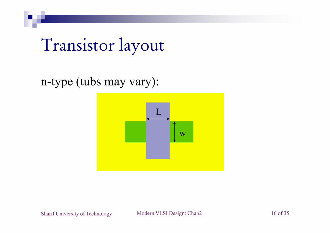
Transistor layout
n-type (tubs may vary):
L
Modern VLSI Design: Chap2 16 of 35Sharif University of Technology
w
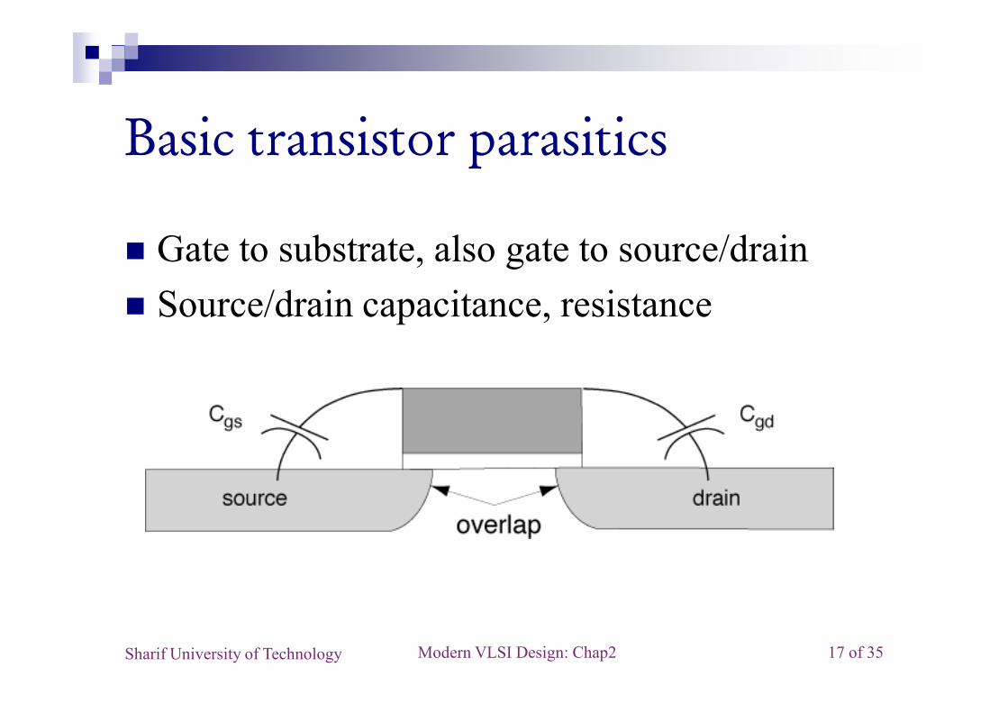
Basic transistor parasitics
� Gate to substrate, also gate to source/drain� Source/drain capacitance, resistance
Modern VLSI Design: Chap2 17 of 35Sharif University of Technology

Basic transistor parasitics (Cont’d)
� Gate capacitance Cg�Determined by active area
� Source/drain overlap capacitances C C d
Modern VLSI Design: Chap2 18 of 35Sharif University of Technology
� Source/drain overlap capacitances Cgs, Cgd�Determined by source/gate and drain/gate overlaps�Independent of transistor L�Cgs = Col W
� Drain/bulk & source/bulk capacitance
Outline
� Fabrication steps� Transistor structures� Transistor behavior
Modern VLSI Design: Chap2 19 of 35Sharif University of Technology
� Transistor behavior�NMOS�PMOS
� Latch up
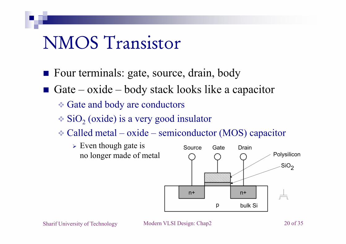
NMOS Transistor� Four terminals: gate, source, drain, body� Gate – oxide – body stack looks like a capacitor
� Gate and body are conductors� SiO2 (oxide) is a very good insulator
Modern VLSI Design: Chap2 20 of 35Sharif University of Technology
2 ( ) y g� Called metal – oxide – semiconductor (MOS) capacitor
� Even though gate isno longer made of metal
n+
p
GateSource Drain
bulk Si
SiO2
Polysilicon
n+
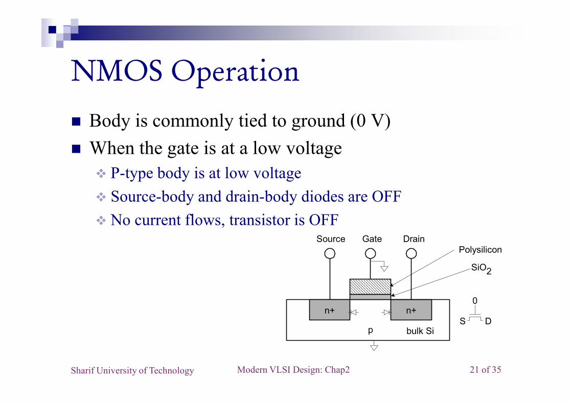
NMOS Operation� Body is commonly tied to ground (0 V)� When the gate is at a low voltage
� P-type body is at low voltage� Source-body and drain-body diodes are OFF
Modern VLSI Design: Chap2 21 of 35Sharif University of Technology
y y� No current flows, transistor is OFF
n+
p
GateSource Drain
bulk Si
SiO2
Polysilicon
n+D
0
S
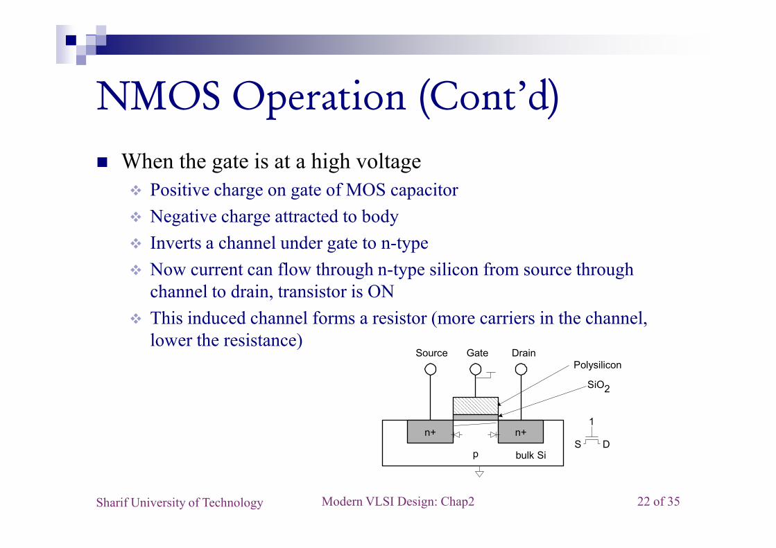
� When the gate is at a high voltage� Positive charge on gate of MOS capacitor� Negative charge attracted to body� Inverts a channel under gate to n-type� Now current can flow through n-type silicon from source through
NMOS Operation (Cont’d)
Modern VLSI Design: Chap2 22 of 35Sharif University of Technology
� Now current can flow through n type silicon from source throughchannel to drain, transistor is ON
� This induced channel forms a resistor (more carriers in the channel,lower the resistance)
n+
p
GateSource Drain
bulk Si
SiO2
Polysilicon
n+D
1
S
� Poly-oxide-silicon sandwich under the gate is acapacitor�To increase voltage, need to add positive charge to
l d i h ili
NMOS Operation (Cont’d)
Modern VLSI Design: Chap2 23 of 35Sharif University of Technology
poly and negative charge to silicon� Initially, negative charge comes from pushing
away holes� After threshold voltage is reached, channel of
mobile electrons formed
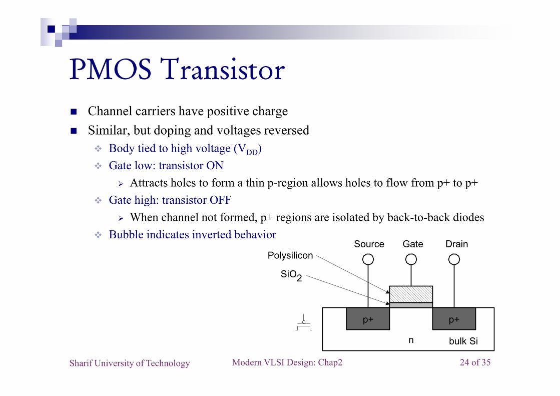
PMOS Transistor� Channel carriers have positive charge� Similar, but doping and voltages reversed
� Body tied to high voltage (VDD)� Gate low: transistor ON
� Attracts holes to form a thin p-region allows holes to flow from p+ to p+� G t hi h t i t OFF
Modern VLSI Design: Chap2 24 of 35Sharif University of Technology
� Gate high: transistor OFF� When channel not formed, p+ regions are isolated by back-to-back diodes
� Bubble indicates inverted behavior
SiO2
n
GateSource Drain
bulk Si
Polysilicon
p+ p+
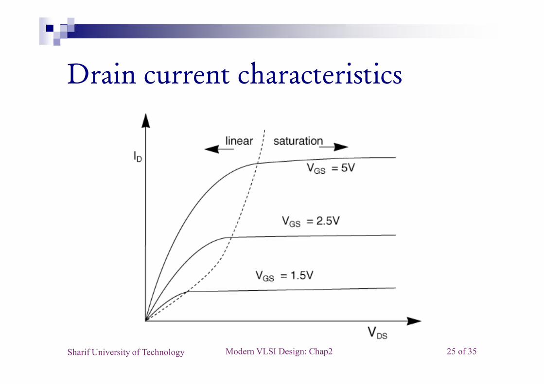
Drain current characteristics
Modern VLSI Design: Chap2 25 of 35Sharif University of Technology
Drain current
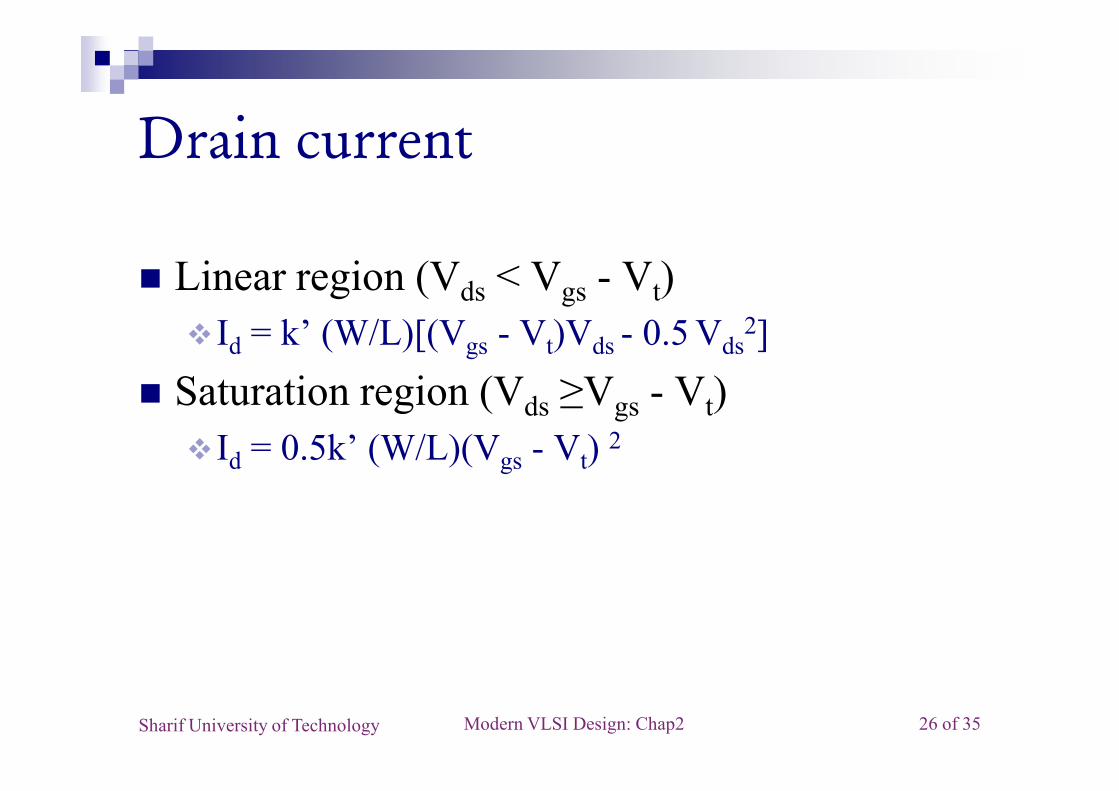
� Linear region (Vds < Vgs - Vt)�Id = k’ (W/L)[(Vgs - Vt)Vds - 0.5 Vds
2]� Saturation region (V ≥V - V )
Modern VLSI Design: Chap2 26 of 35Sharif University of Technology
� Saturation region (Vds ≥Vgs - Vt)�Id = 0.5k’ (W/L)(Vgs - Vt) 2
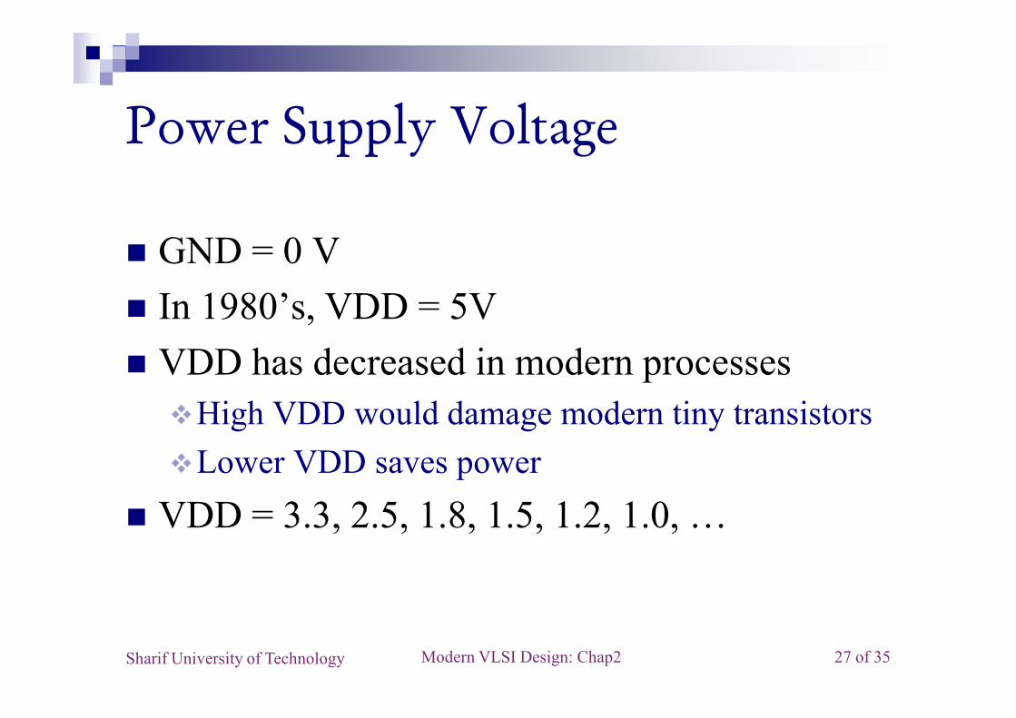
Power Supply Voltage
� GND = 0 V� In 1980’s, VDD = 5V� VDD has decreased in modern processes
Modern VLSI Design: Chap2 27 of 35Sharif University of Technology
� VDD has decreased in modern processes�High VDD would damage modern tiny transistors�Lower VDD saves power
� VDD = 3.3, 2.5, 1.8, 1.5, 1.2, 1.0, …
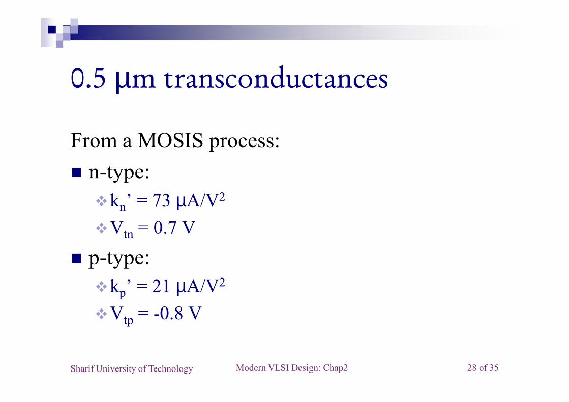
0.5 µm transconductances
From a MOSIS process:� n-type:
�k ’ = 73 µA/V2
Modern VLSI Design: Chap2 28 of 35Sharif University of Technology
�kn = 73 µA/V�Vtn = 0.7 V
� p-type:�kp’ = 21 µA/V2
�Vtp = -0.8 V
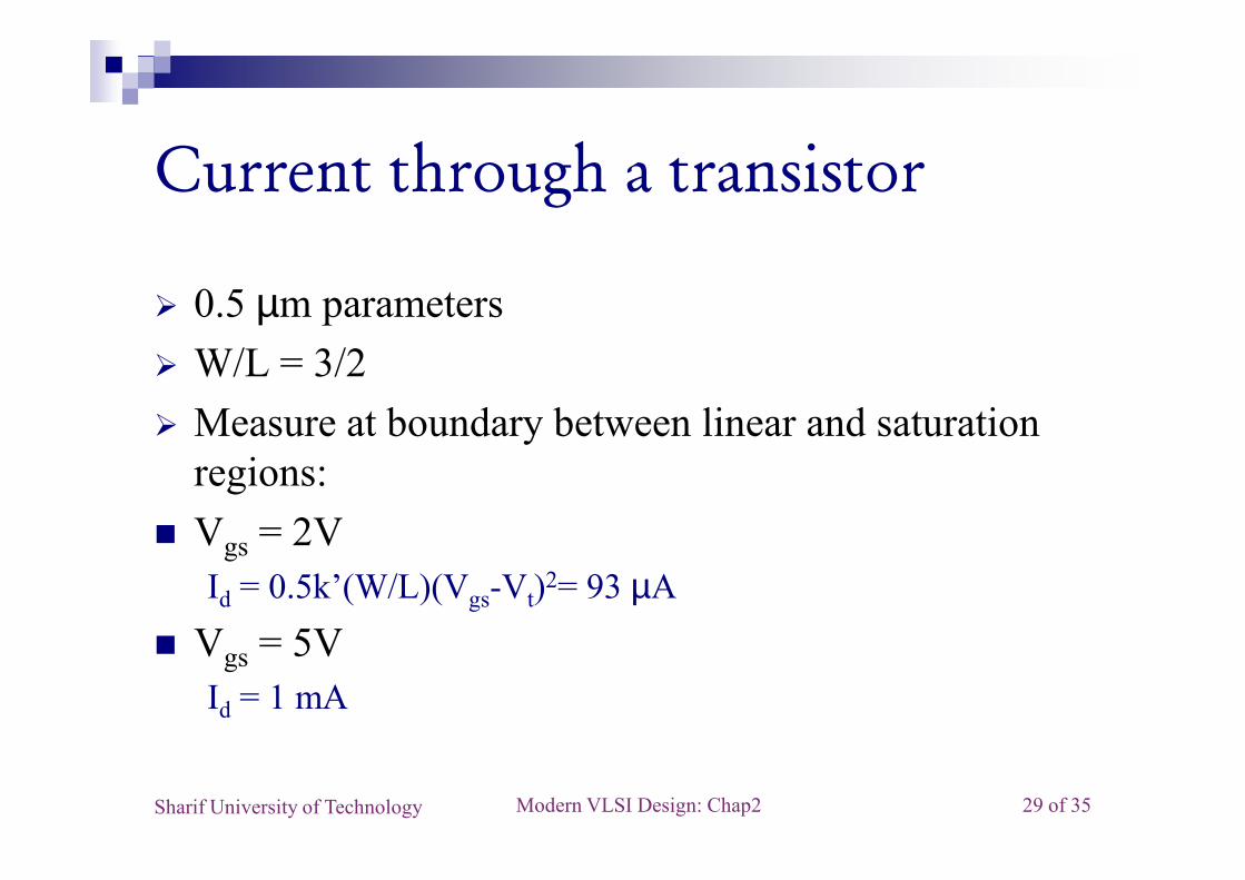
Current through a transistor
� 0.5 µm parameters� W/L = 3/2� Measure at boundary between linear and saturation
Modern VLSI Design: Chap2 29 of 35Sharif University of Technology
yregions:
� Vgs = 2VId = 0.5k’(W/L)(Vgs-Vt)2= 93 µA
� Vgs = 5VId = 1 mA
Outline
� Fabrication steps� Transistor structures� Transistor behavior
Modern VLSI Design: Chap2 30 of 35Sharif University of Technology
� Transistor behavior�NMOS�PMOS
� Latch up
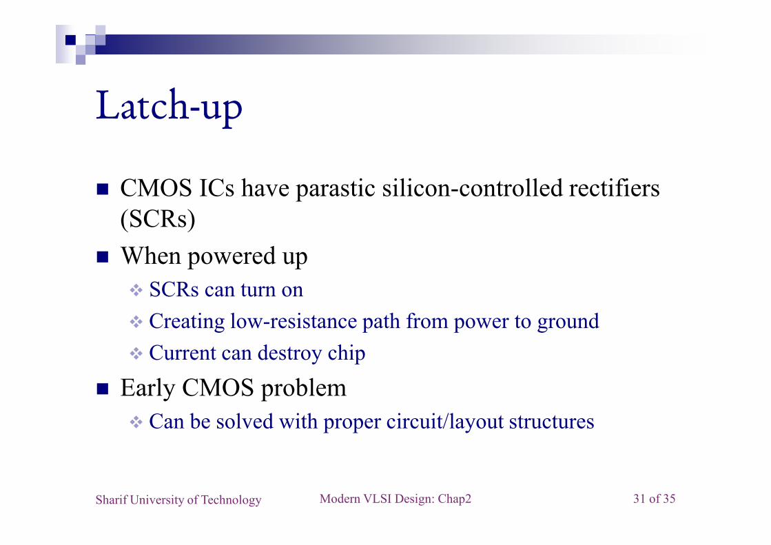
Latch-up
� CMOS ICs have parastic silicon-controlled rectifiers(SCRs)
� When powered up
Modern VLSI Design: Chap2 31 of 35Sharif University of Technology
� SCRs can turn on� Creating low-resistance path from power to ground� Current can destroy chip
� Early CMOS problem� Can be solved with proper circuit/layout structures
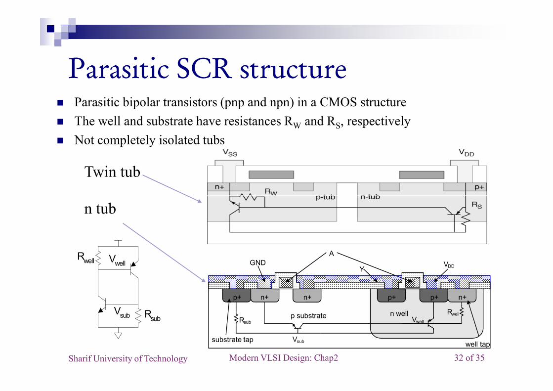
Parasitic SCR structure� Parasitic bipolar transistors (pnp and npn) in a CMOS structure� The well and substrate have resistances RW and RS, respectively� Not completely isolated tubs
Twin tub
Modern VLSI Design: Chap2 32 of 35Sharif University of Technology
n+
p substrate
p+
A
YGND VDD
n+p+
substrate tap well tap
n+ p+
n wellRsub
Rwell
Vsub
VwellRsub
Rwell
Vsub
Vwell
n tub
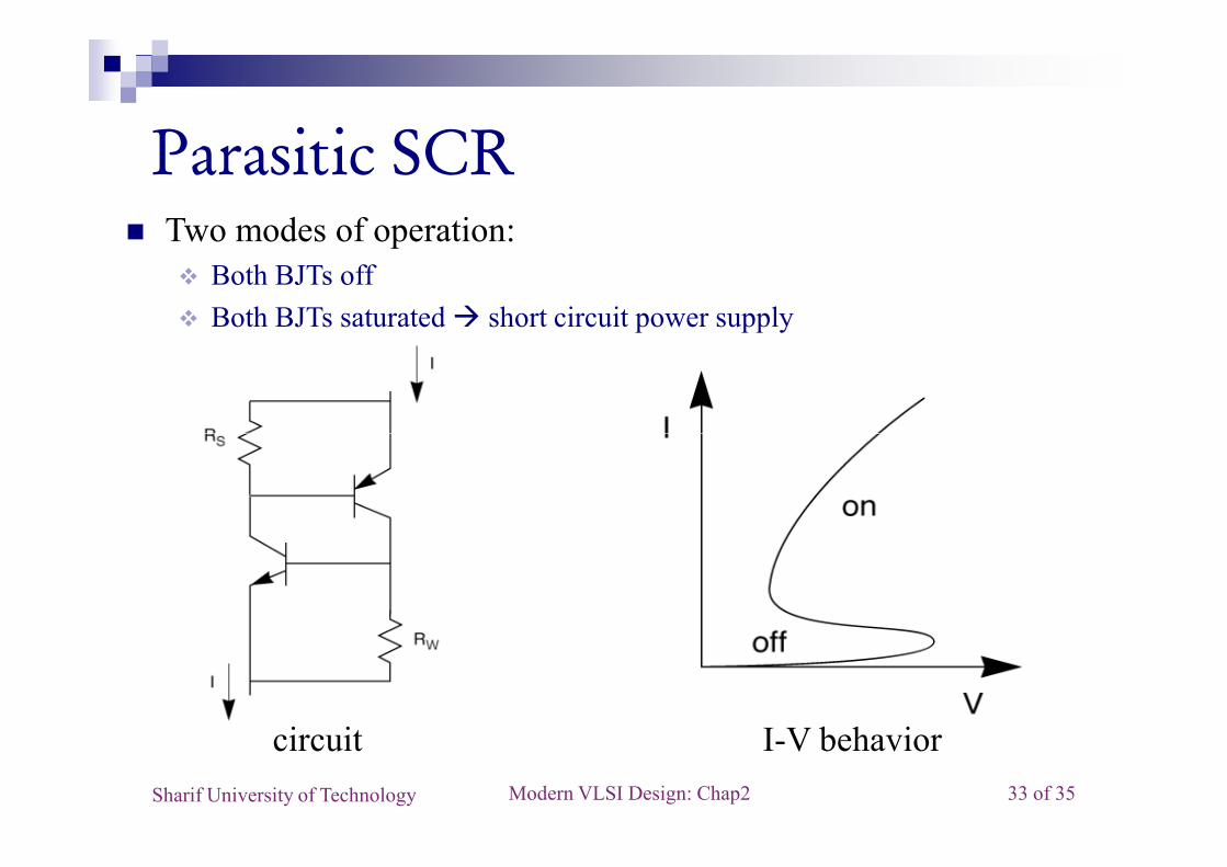
Parasitic SCR� Two modes of operation:
� Both BJTs off� Both BJTs saturated � short circuit power supply
Modern VLSI Design: Chap2 33 of 35Sharif University of Technology
circuit I-V behavior
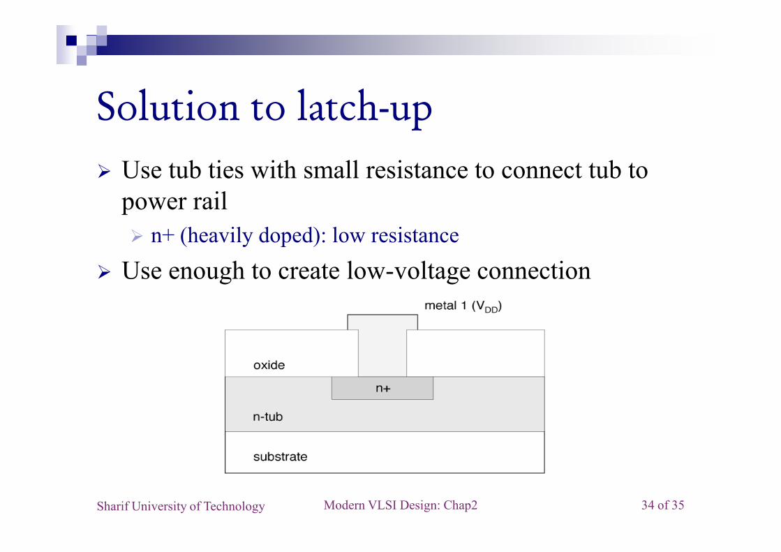
Solution to latch-up� Use tub ties with small resistance to connect tub to
power rail� n+ (heavily doped): low resistance
� Use enough to create low-voltage connection
Modern VLSI Design: Chap2 34 of 35Sharif University of Technology
� Use enough to create low voltage connection
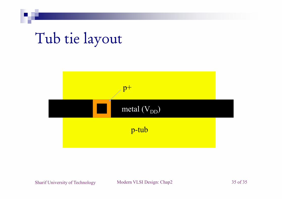
Tub tie layout
p+
Modern VLSI Design: Chap2 35 of 35Sharif University of Technology
metal (VDD)
p-tub