battery charger detection over usb with ft-x devices
TRANSCRIPT

Use of FTDI devices in life support and/or safety applications is entirely at the user’s risk, and the user agrees to defend, indemnify and hold FTDI harmless from any and all damages, claims, suits
or expense resulting from such use.
Future Technology Devices International Limited (FTDI) Unit 1, 2 Seaward Place, Glasgow G41 1HH, United Kingdom Tel.: +44 (0) 141 429 2777 Fax: + 44 (0) 141 429 2758
Web Site: http://ftdichip.com Copyright © Future Technology Devices International Limited
Application Note
AN_175
Battery Charger Detection over
USB with FT-X Devices
Version 1.1
Issue Date: 2016-07-07
The purpose of this document is to describe how to use the FT-X family of devices in designs that are required to detect if the device is connected to a power source for battery charging or a full USB host controller.

Application Note
AN_175 Battery Charger Detection over USB with FT-X Devices Version 1.1
Document Reference No.: FT_000454 Clearance No.: FTDI# 275
1 Product Page Document Feedback Copyright © Future Technology Devices International Limited
Table of Contents
1 Introduction .............................................................. 2
2 Reference Design....................................................... 3
2.1 Schematic ............................................................................ 3
2.2 Circuit Description ............................................................... 3
2.3 CBUS signals used in the battery charging application ........ 5
2.4 Dedicated Charging Port ...................................................... 6
2.5 USB Host Port (FT-X Enumerated) ....................................... 7
2.6 USB Host Port (FT-X not yet enumerated) ........................... 8
2.7 USB Host Port (FT-X in Suspend) ........................................ 9
2.8 Considerations for BCD#, PWREN# and SLEEP# .................. 9
3 MTP Memory Settings .............................................. 10
4 Reduced CBUS Pin-Count ......................................... 14
4.1 Example with 3 CBUS pins ................................................. 14
4.2 Example with 2 CBUS pins ................................................. 16
4.3 Example with 1 CBUS pin .................................................. 18
5 Driver Requirements ............................................... 20
6 Power Considerations .............................................. 21
6.1 Voltage .............................................................................. 21
6.2 Current .............................................................................. 21
7 Contact Information ................................................ 22
Appendix A – References ............................................. 23
Document References ............................................................... 23
Acronyms and Abbreviations ..................................................... 23
Appendix B – List of Tables & Figures .......................... 24
List of Tables ............................................................................. 24
List of Figures ........................................................................... 24
Appendix C – Revision History ..................................... 25

Application Note
AN_175 Battery Charger Detection over USB with FT-X Devices Version 1.1
Document Reference No.: FT_000454 Clearance No.: FTDI# 275
2 Product Page Document Feedback Copyright © Future Technology Devices International Limited
1 Introduction
The FT-X family of devices have a new feature to support the USB-IF Battery Charging Specification, v1.2. Special circuitry inside the FT-X detects when the device is connected to a dedicated charging port. A dedicated charging port is a downstream USB port on a device that outputs power through a USB connector but is not capable of enumerating a device connected to it. Examples include plug
top chargers which connect to a mains socket and chargers which connect to the low voltage power sockets in automobiles. Further information on the different types of charging port and the specifications for the Dedicated Charging Port can be found in reference [1] in Appendix A – References. When it detects that it is connected to a dedicated charging port, the FT-X can enable a charging circuit (or to notify a microcontroller or logic on the application board which in turn controls the
charging).
This document provides information on how to use the FT-X family of devices in designs that are required to detect if the device is connected to a power source for battery charging or a full USB host controller.

Application Note
AN_175 Battery Charger Detection over USB with FT-X Devices Version 1.1
Document Reference No.: FT_000454 Clearance No.: FTDI# 275
3 Product Page Document Feedback Copyright © Future Technology Devices International Limited
2 Reference Design
2.1 Schematic
Figure 1: USB Battery Charging Example
2.2 Circuit Description
The example schematic in Figure 1 illustrates a battery charging application based around the FT-X device. The circuit charges a battery when connected to either a USB Host port or a Dedicated Charging Port. The FT231X device also features a full set of UART pins, although the same battery charging principle also applies to the other FT-X family devices. The example circuit uses the LTC4053 battery charge controller which is designed for Lithium-Ion
batteries. The application circuit shown in the schematic is available as a development module from FTDI. More details on this module can be found in the module datasheet. Please see reference [4] in Appendix A – References
The circuit shows how the CBUS pins of the FT-X are used to control the charging rate of the battery depending on the power source detected and the associated current limit of the power source. The charge rate of the battery is defined by the resistance connected to the PROG pin of the LTC4053 battery charging controller. In this case, the resistance of the PROG pin is set by resistors R12, R13 and R14, where the state of the BCD# and PWREN# CBUS pins defines the overall resistance.

Application Note
AN_175 Battery Charger Detection over USB with FT-X Devices Version 1.1
Document Reference No.: FT_000454 Clearance No.: FTDI# 275
4 Product Page Document Feedback Copyright © Future Technology Devices International Limited
The CBUS pins are configured to assign the BCD#, PWREN# and SLEEP# outputs to them. More detail on the use of these signals is given in section 2.3. Further information on how to program the MTP memory settings for the CBUS pins is available in Section 3. This document focuses on an application where four CBUS pins are available for battery charging
signals. Section 4 shows some alternative examples for cases where battery charging can be implemented with a smaller number of CBUS pins, for example where four CBUS pins are not available. A feature of the FT-X devices is that the BCD#, PWREN# and SLEEP# outputs have been designed to minimise the external circuitry required for charging applications. It can be noted that no
external MOSFETs are required in Figure 1 and Figure 2 to select the range as the open-drain outputs can be used directly. The calculation used to determine the resistor values and associated charging current is shown below:
10005.1
prog
chgR
i
Where ichg is the charging current (A), and,
Rprog is the resistance from the LTC4053 Prog pin to ground
A simplified schematic for the charging circuit is shown below:
BCD#
PWREN#
SLEEP#
GND GND
1K5
4K32
16K52K2
VCC
VBUS
VCC
VBUS
PROG
SHDN#
FTDI X-Chip LTC4053EDD
GND
BAT
R14
R13
R11 R12
Figure 2: Simplified charging circuit
The circuit has four different modes to allow the charging current to be adjusted depending on the available current from the power source. These are described in more detail later in this section.
Dedicated Charging Port See section 2.4 USB Host Port (FT-X Enumerated) See section 2.5
USB Host Port (FT-X not yet enumerated) See section 2.6 USB Host Port (FT-X in Suspend) See section 2.7

Application Note
AN_175 Battery Charger Detection over USB with FT-X Devices Version 1.1
Document Reference No.: FT_000454 Clearance No.: FTDI# 275
5 Product Page Document Feedback Copyright © Future Technology Devices International Limited
2.3 CBUS signals used in the battery charging application
The FT-X includes many different signals which can be routed to the CBUS pins. The signals used
for this charging application are described here. Section 3 has further details on how to configure the CBUS pins. Some FT-X devices do not have four CBUS pins available. In other cases, the application may be using some CBUS pins for other purposes. This may require the battery charging function to be implemented with a smaller number of CBUS pins. Section 4 has further details of battery charging circuits using 1, 2 or 3 CBUS pins.
CBUS Pin FT-X Signal Comments
0 BCD# Indicates that FT-X has detected a Dedicated Charging Port. Used to
select resistance value on PROG pin for 1A charging
1 PWREN# Not used for charging circuit (see the PWREN# section below for more
details)
2 SLEEP# Indicates that the FT-X has been put into Sleep/Suspend by the USB
Host. Used to enable ShutDown mode of LTC4053
3 PWREN# Indicates that the FT-X has been enumerated by the USB Host. Used
to select resistance value on PROG pin for 500mA charging
Table 2.1 Summary of CBUS pins used in this application
BCD#
This open-drain active-low output is asserted when the FT-X detects that it is connected to a dedicated charging port. It does not have an internal pull-up.
In this application, it is used to configure the resistor network on the PROG pin of the LTC4053 to set approximately 1A of charging current. Since the BCD# signal is open-drain without an internal pull-up, it can be used to pull resistor R14 to ground without the need for an external MOSFET. When the FT-X is connected to a standard USB Host Controller, this pin is not asserted and the device operates in the same way as previous FTDI devices such as the FT232R.
PWREN# This open-drain active-low output is asserted whilst the FT-X is successfully enumerated on a USB Host Controller. It is floating before enumeration and during suspend. It is driven low when the FT-X is enumerated and not in suspend. It does not have an internal pull-up. This signal is assigned to two different CBUS pins as shown in Table 2.1.
CBUS1 (PWREN# net in the schematic) is not used as part of the battery charging circuit. It is used to enable power to external circuits which may be sourced from the USB VBUS supply. It operates in the same way as other FTDI devices, allowing high power circuitry to be turned off when the FTDI device has been put into suspend or is not yet enumerated. The pin controls MOSFET Q1 which in turn enables power to the SWPWR pin on CN4 when PWREN# is low. External
pull-up resistor R6 ensures that the MOSFET gate is pulled high when PWREN# is not asserted.
Application Note
AN_175 Battery Charger Detection over USB with FT-X Devices Version 1.1
Document Reference No.: FT_000454 Clearance No.: FTDI# 275
6 Product Page Document Feedback Copyright © Future Technology Devices International Limited
CBUS3 (PWREN#2 net in the schematic) is used to configure the resistor network on the PROG pin of the LTC4053 to set approximately 440mA of charging current. This allows the overall current drawn to remain within the maximum 500mA available from a USB Host Port (see Section 6). Since the FT-X itself will draw approximately 8mA, then approximately 52mA will be left for the remainder of the application circuit.
Because the PWREN# signal is open-drain without an internal pull-up, it can be used to pull resistor R13 to ground without the need for an external MOSFET. Because the current flowing in this pin directly controls the battery charging current, it is recommended to keep it separate from the pin used to control the power switching circuit. This is the reason for using two different CBUS pins both configured as PWREN#.
Note that an option in the MTP memory defines whether this signal is also asserted when connected to a DCP. Section 3 has further details. This is not enabled in the example used throughout this application note but is available if required.
SLEEP#
This push-pull active-low output is asserted when the FT-X has been put into USB suspend. It is driven low whilst in suspend and is driven high (VCCIO) when not in suspend. This signal is used to shut down the LTC4053 when the device is powered from a USB host and the host has put the FT-X in suspend. An option bit in the MTP memory of the FT-X (De-Activate Sleep) allows this signal to remain non-
asserted whilst a battery charger has been detected. This option must be enabled if SLEEP# is connected to the Shut Down input of the battery charger IC to avoid the charge controller IC being shut down when the circuit is connected to a dedicated charging port. This is because the FT-X will be in suspending mode whilst not connected to a USB host.
2.4 Dedicated Charging Port
This mode is enabled when the FT-X detects that it is connected to a Dedicated Charging Port. The dedicated charging port can provide higher currents than a standard USB port and therefore the
current is set to approximately 1A. Refer to section 6 for more details regarding charging current calculations.
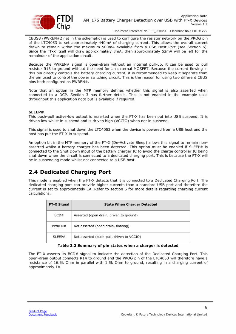
Table 2.2 Summary of pin states when a charger is detected
The FT-X asserts its BCD# signal to indicate the detection of the Dedicated Charging Port. This open-drain output connects R14 to ground and the PROG pin of the LTC4053 will therefore have a
resistance of 16.5k Ohm in parallel with 1.5k Ohm to ground, resulting in a charging current of approximately 1A.
FT-X Signal State When Charger Detected
BCD# Asserted (open drain, driven to ground)
PWREN# Not asserted (open drain, floating)
SLEEP# Not asserted (push-pull, driven to VCCIO)

Application Note
AN_175 Battery Charger Detection over USB with FT-X Devices Version 1.1
Document Reference No.: FT_000454 Clearance No.: FTDI# 275
7 Product Page Document Feedback Copyright © Future Technology Devices International Limited
AiR
i
kOhmRkOhmkOhmR
chgprog
chg
progprog
09.110005.1
375.15.1
1
5.16
11
The open-drain feature of the BCD# signal allows this configuration to be used without external MOSFETs being required. PWREN# will not be asserted since the FT-X is not enumerated by a USB Host Port. SLEEP# will not be asserted and will be driven high, which prevents the LTC4053 going into
Shutdown mode. Normally, SLEEP# would be expected to be asserted since the device is not enumerated and therefore the USB circuits in the FT-X will be in a suspend state. However, an option (De-Activate Sleep) can be selected in the MTP memory of the FT-X which prevents SLEEP# from being asserted when a Dedicated Charging Port is detected.
2.5 USB Host Port (FT-X Enumerated)
This state applies when the FT-X is connected to a USB Host Controller and is fully enumerated (and not in USB Suspend mode). As shown in section 6, when a peripheral is connected to a USB Host Port, it may draw a maximum of 500mA once fully enumerated. Note that the current drawn by the application circuit itself should be considered when setting the
charging current. The current limits quoted in the USB specification are total values and therefore the battery charge current may need to be set below 500mA so that the total drawn from the USB port is within the specification. This example uses a charge current of approximately 440mA.
Table 2.3 Summary of pin states when enumerated
BCD# will not be asserted since the FT-X has not detected a dedicated charging port.
PWREN# will be low since the FT-X is enumerated and not in suspend mode. This open-drain output connects R13 to ground and the PROG pin of the LTC4053 will therefore have a resistance of 16.5k Ohm in parallel with 4.32k Ohm to ground, resulting in a charging current of approximately 440mA.
mAiR
i
kOhmRkOhmkOhmR
chgprog
chg
progprog
43810005.1
424.332.4
1
5.16
11
FT-X Signal State when enumerated
BCD# Not asserted (open drain, floating)
PWREN# Asserted (open drain, driven to ground)
SLEEP# Not asserted (push-pull, driven to VCCIO)

Application Note
AN_175 Battery Charger Detection over USB with FT-X Devices Version 1.1
Document Reference No.: FT_000454 Clearance No.: FTDI# 275
8 Product Page Document Feedback Copyright © Future Technology Devices International Limited
The open-drain feature of the PWREN# signal allows this configuration to be used without external MOSFETs being required. SLEEP# will be high and will prevent the LTC4053 going into Shutdown mode. This allows the LTC4053 to provide the charging current to the battery.
2.6 USB Host Port (FT-X not yet enumerated)
This state applies when the FT-X is connected to a USB Host Controller and is not yet enumerated.
As shown in section 6, when a peripheral is connected to a USB Host Port, it may draw a maximum of 100mA until fully enumerated. Note that the current drawn by the application circuit itself should be considered when setting the charging current. The current limits quoted in the USB specification are total values and therefore the battery charge current may need to be set below 100mA so that the total drawn from the USB
port is within the specification. This example uses a charge current of approximately 91mA, which
allows up to 9mA for the application circuit itself (the FT-X typically uses 8mA).
Table 2.4 Summary of pin states when connected to USB Host while awaiting
enumeration
BCD# will not be asserted since the FT-X has not detected a dedicated charging port.
PWREN# will also not be asserted since the FT-X is not yet enumerated. The overall resistance from the PROG pin of the LTC4053 to ground is therefore 16.5k Ohms to ground, resulting in a charging current of approximately 91mA.
mAiR
i
kOhmR
chgprog
chg
prog
9110005.1
5.16
SLEEP# will be high and will prevent the LTC4053 going into Shutdown mode. This allows the
LTC4053 to provide the charging current to the battery.
FT-X Signal State when connected to USB Host while awaiting enumeration
BCD# Not asserted (open drain, floating)
PWREN# Not asserted (open drain, floating)
SLEEP# Not asserted (push-pull, driven to VCCIO)

Application Note
AN_175 Battery Charger Detection over USB with FT-X Devices Version 1.1
Document Reference No.: FT_000454 Clearance No.: FTDI# 275
9 Product Page Document Feedback Copyright © Future Technology Devices International Limited
2.7 USB Host Port (FT-X in Suspend)
This state applies when the FT-X is connected to a USB Host Controller and is in USB Suspend mode. As shown in section 6, when a peripheral is connected to a USB Host Port, it may draw a maximum of 2.5mA when in suspend.
Table 2.5 Summary of pin states when FT-X in Suspend
Because the application must consume less than 2.5mA, the shutdown mode of the LTC4053 is
activated. BCD# will be de-asserted since no battery charger was detected. PWREN# will also be de-asserted since the FT-X is in suspend mode. SLEEP# will be asserted and will pull the SHDN# pin of the LTC4053 low, which disables the
battery charging.
2.8 Considerations for BCD#, PWREN# and SLEEP#
The PWREN# and BCD# signals are open-drain outputs from the FT-X and have no internal pull-up. The SLEEP# signal is a push-pull output which drives to VCCIO when high (not asserted). The states of these pins can depend on the settings in the BCD section of the MTP memory. Please ensure that these are set correctly for the application. Section 3 has further details. During start-up of the device, the CBUS pins will default to an input with weak pull-up until the
MTP memory is read. This will occur for approximately 14ms and the CBUS pins will then take their selected function and behave as described elsewhere in this document. In some members of the FT-X family, four CBUS pins are not available. Section 4 has examples of battery charging circuits which use fewer than four CBUS pins.
FT-X Signal State when in Suspend
BCD# Not asserted (open drain, floating)
PWREN# Not asserted (open drain, floating)
SLEEP# Asserted (push-pull, driven to ground)

Application Note
AN_175 Battery Charger Detection over USB with FT-X Devices Version 1.1
Document Reference No.: FT_000454 Clearance No.: FTDI# 275
10 Product Page Document Feedback Copyright © Future Technology Devices International Limited
3 MTP Memory Settings
The Battery Charge Detection feature is not enabled by default. In order to use this feature, the related signals must be mapped onto the CBUS pins. In this example, the configuration used is shown in Table 2.1. This configuration is stored in the MTP memory inside the FT-X device. The current required when the circuit is connected to the USB Host port (as detailed in section 2.5) should also be specified in the MTP memory, so that the FT-X can provide this information to the host computer which can then decide whether it will enumerate the FT-X and allow this current to
be drawn. The MTP memory is programmed using the free FT_Prog utility which can be downloaded along with a full user guide from the Utilities page at the link below. Because the MTP memory programming is carried out over the existing USB link to the FT-X device, no additional hardware is required.
http://www.ftdichip.com/Support/Utilities.htm#FT_Prog The following screen-shots show the BCD-related configuration settings in FT_Prog. Figure 3 below shows the CBUS pins being set to their battery charging functions. The settings correspond to those shown in section 2.3 in order to match the schematic in Figure 1.
Figure 4 shows the BCD settings being configured.
Battery Charge Enable must be enabled in order to use the battery charger detection feature.
Force Power Enable allows the PWREN# signal to be asserted when a DCP is detected. Otherwise, it will only be asserted when enumerated by a USB Host Port. In this application, this option is not selected since the resistor values have been specified to give
approx 1A when only BCD is asserted. Asserting PWREN# in addition to this would lead to a higher charge current (see Section 2.4).
De-Activate Sleep is enabled to prevent the device going to sleep when connected to a DCP (since it would normally go to sleep when not connected to a USB Host Port).
Otherwise, the LTC4053 would be in Shutdown mode and the battery would not charge.
Figure 5 shows the current required by the circuit being specified. In this case, up to 500mA is requested from the USB Host Port (see calculation in Section 2.5)

Application Note
AN_175 Battery Charger Detection over USB with FT-X Devices Version 1.1
Document Reference No.: FT_000454 Clearance No.: FTDI# 275
11 Product Page Document Feedback Copyright © Future Technology Devices International Limited
Figure 3: Configuring the CBUS pins in MTP memory using FT Prog

Application Note
AN_175 Battery Charger Detection over USB with FT-X Devices Version 1.1
Document Reference No.: FT_000454 Clearance No.: FTDI# 275
12 Product Page Document Feedback Copyright © Future Technology Devices International Limited
Figure 4: Configuring the BCD Settings in MTP memory using FT Prog

Application Note
AN_175 Battery Charger Detection over USB with FT-X Devices Version 1.1
Document Reference No.: FT_000454 Clearance No.: FTDI# 275
13 Product Page Document Feedback Copyright © Future Technology Devices International Limited
Figure 5: Configuring the current required in MTP memory using FT Prog

Application Note
AN_175 Battery Charger Detection over USB with FT-X Devices Version 1.1
Document Reference No.: FT_000454 Clearance No.: FTDI# 275
14 Product Page Document Feedback Copyright © Future Technology Devices International Limited
4 Reduced CBUS Pin-Count
It is also possible to implement a USB charging solution with the FT-X without needing all four CBUS pins. This could be required if there are not enough pins available. These configurations may also be preferred in some cases if a variable charging rate is not required or if charging is only required when connected to a DCP (i.e. charging from the USB Host Port is not required).
4.1 Example with 3 CBUS pins
In the example below, three CBUS pins are available. The operation from a battery charging point
of view is the same as the version using four CBUS pins described throughout this application note. The main difference is that only one PWREN# signal is used instead of two. This can be achieved
without losing battery charger functionality but the MOSFET used to switch VBUS power to other external circuits (SWPWR on the schematic) in section 2.1 has been removed. If this MOSFET is required, then it is not recommended to drive it directly from the same CBUS pin as is used to set the charging current because this may interfere with the current flowing out of
the Prog pin of the LTC4053. In this case, the design in section 4.2 could be used which requires only 2 CBUS pins for battery charging, leaving an additional CBUS line to drive the MOSFET. The charging currents are the same as for the version with 4 CBUS pins, and are summarized below:
Table 4.1 Summary of charging currents (example with 3 CBUS pins)
Please note the MTP memory settings required for this configuration which are shown in the table in the schematic.
Connected to Charging Current Comments
Dedicated Charging
Port Approx 1A See section 2.4 for calculation
USB Host Port
(Enumerated) Approx 440mA See section 2.5 for calculation
USB Host Port (Not
Enumerated) Approx 91mA See section 2.6 for calculation
USB Host Port
(Suspend) No Charge See section 2.7

Application Note
AN_175 Battery Charger Detection over USB with FT-X Devices Version 1.1
Document Reference No.: FT_000454 Clearance No.: FTDI# 275
15 Product Page Document Feedback Copyright © Future Technology Devices International Limited
X-Chip Pin Function
MTP memory Setting
CBUS0CBUS1CBUS2
BCD#PWREN#SLEEP#
Battery Options
Battery Charger Enable
Force Power Enable
De-acticate Sleep X
X
PWREN#
GN
D
CBUS210
DPDM
3V3OUT
RESET#
VC
C
GN
D
CBUS117
CBUS018
VC
CIO
BCD#
SLEEP#
GND
GND
0.1uF 0.1uF
GND
GND
600R/2A
10nF
VBUS 3V3OUT
0.1uF0R
GNDSLD GND
27R27R
VBUS1
D-2
D+3
GND5
ID4
CN USB
3V3OUT 3V3OUTVBUS VBUS
N.F.
1K5 - 1%16K5 1%
GND
BCD#
4K32 1%
PWREN#
1A when connected to a dedicated charger port0.4A when enumerated
0A when in sleep0.1A when not enumerated and not in sleep
VCC2
FAULT3
TIMER4
GND5
NTC6
PROG7
SHDN8
BAT9
ACPR10
CHRG1
GN
D1
1
LTC4053EDD
GND
4.7uF
0.1uF
GND
VBUSVBUS
GND
VBATT
GND
GND1
TB3.5mmNTC
0.1uF
GND
VBUS
1uF
1R
GND
VBUS
2K2
GND
JP1
1-22-3
NCT Enabled
NCT Available
JP1SIP-3
NTC
GND
NCT Disabled (Default)JUMPER-2mm
4K32 1%
+
-NCT
SLEEP#
Figure 6: Example of battery charging with only 3 CBUS pins

Application Note
AN_175 Battery Charger Detection over USB with FT-X Devices Version 1.1
Document Reference No.: FT_000454 Clearance No.: FTDI# 275
16 Product Page Document Feedback Copyright © Future Technology Devices International Limited
4.2 Example with 2 CBUS pins
If only two CBUS pins are available, the PWREN# and SLEEP functions may be used to control the LTC4053 such that a battery may be charged from a standard host or from a dedicated charging port. In this case, since BCD# is not available, there is no way to distinguish between a DCP and a USB Host Port which is fully enumerated. The current must therefore be limited to the amount which would be available from the USB Host Port instead of the full 1A available from a DCP.
The SLEEP pin is used to disable the LTC4053 when in USB Suspend. The PWREN# signal allows the charge current to be kept below 100mA when not enumerated and then increased to approx 440mA once enumerated by altering the resistance on the LTC4053 PROG pin.
Table 4.2 Summary of charging currents (example with 2 CBUS pins)
Please note the MTP memory settings required for this configuration which are shown in the table in the schematic.
Connected to Charging Current Comments
Dedicated Charging
Port Approx 440mA See section 2.5 for calculation
USB Host Port
(Enumerated) Approx 440mA See section 2.5 for calculation
USB Host Port (Not
Enumerated) Approx 91mA See section 2.6 for calculation
USB Host Port
(Suspend) No Charge See section 2.7

Application Note
AN_175 Battery Charger Detection over USB with FT-X Devices Version 1.1
Document Reference No.: FT_000454 Clearance No.: FTDI# 275
17 Product Page Document Feedback Copyright © Future Technology Devices International Limited
X-Chip Pin Function
MTP memory Setting
CBUS5CBUS6
SLEEP#PWREN#
Battery Options
Battery Charger Enable
Force Power Enable
De-acticate Sleep X
X
X
SLEEP#PWREN#
DPDM
3V3OUT
VC
OR
E
RESET#
VC
C
CBUS6CBUS5
VC
CIO
U1
0.4A when connected to a dedicated charger port
GND
GND
0.1uF 0.1uF
GND
GND
600R/2A
10nF
VBUS 3V3OUT
0.1uF0R
GNDSLD GND
27R27R
VBUS1
D-2
D+3
GND5
ID4
CN USB
3V3OUT 3V3OUTVBUS VBUS
N.F.
16K5 1%
GND
4K32 1%
PWREN#
0.4A when enumerated
0A when in sleep mode0.1A when not enumerated and not in sleep mode
VCC2
FAULT3
TIMER4
GND5
NTC6
PROG7
SHDN8
BAT9
ACPR10
CHRG1
GN
D11 LTC4053EDD
GND
4.7uF
0.1uF
GND
VBUSVBUS
GND
VBATT
GND
GND1
TB3.5mmNTC
0.1uF
GND
VBUS
1uF
1R
GND
VBUS
2K2
GND
JP1
1-22-3
NCT Enabled
NCT Available
JP1SIP-3
NTC
GND
NCT Disabled (Default)JUMPER-2mm
4K32 1%
+
-NCT
SLEEP#
Figure 7: Example of battery charging with only 2 CBUS pins

Application Note
AN_175 Battery Charger Detection over USB with FT-X Devices Version 1.1
Document Reference No.: FT_000454 Clearance No.: FTDI# 275
18 Product Page Document Feedback Copyright © Future Technology Devices International Limited
4.3 Example with 1 CBUS pin
In this example, only one CBUS pin is used. This means that a variable charging current which depends on the enumeration state is not used. When connected to a DCP, the BCD# line is asserted and allows battery charging to take place at the current set by the resistor on the PROG pin. The FT-X will be in suspended. When not connected to a DCP (for example, when connected to a USB Host Port), the BCD# line
will not be asserted and the LTC4053 will be put into Shutdown mode and no charging will take place. Because the SLEEP and PWREN# signals are not output, it is not possible for the charging circuit to determine the enumeration state and it is not therefore possible to determine how much current the circuit is allowed to draw (as detailed in Section 6).
Table 4.3 Summary of charging currents (example with 2 CBUS pins)
Please note the MTP memory settings required for this configuration which are shown in the table in the schematic.
Connected to Charging Current Comments
Dedicated Charging
Port Approx 1A See section 2.4 for calculation
USB Host Port
(Enumerated) No Charge See section 2.7
USB Host Port (Not
Enumerated) No Charge See section 2.7
USB Host Port
(Suspend) No Charge See section 2.7

Application Note
AN_175 Battery Charger Detection over USB with FT-X Devices Version 1.1
Document Reference No.: FT_000454 Clearance No.: FTDI# 275
19 Product Page Document Feedback Copyright © Future Technology Devices International Limited
X-Chip Pin Function
MTP memory Setting
CBUS0 BCD
Battery Options
Battery Charger Enable
Force Power Enable
De-acticate Sleep
X
GND
GND
0.1uF 0.1uF
GND
GND
600R/2A
10nF
VBUS 3V3OUT
0.1uF0R
GNDSLD GND
27R27R
VBUS1
D-2
D+3
GND5
ID4
CN USB
VCC2
FAULT3
TIMER4
GND5
NTC6
PROG7
SHDN8
BAT9
ACPR10
CHRG1
GN
D11
LTC4053EDD
GND
3V3OUT 3V3OUT
4.7uF
0.1uF
GND
VBUSVBUS
GND
VBATT
GND
GND
1K5
GND
1
TB3.5mm
VBUS VBUS
NTC
0.1uF
GND
VBUS
1uF
1R
GND
VBUS
BCD
2K2
GND
JP1
1-22-3
NCT Enabled
NCT Available
JP1SIP-3
NTC
GND
NCT Disabled (Default)JUMPER-2mm
4K32 1%
GN
D
DPDM
3V3OUT
RESET#
VC
C
GN
D
CBUS0
VC
CIO
BCD
1A when connected to a dedicated charger port0A when enumerated
0A when in sleep0A when not enumerated and not in sleep
+
-NCT
N.F.
Figure 8: Example of battery charging with only 1 CBUS pin

Application Note
AN_175 Battery Charger Detection over USB with FT-X Devices Version 1.1
Document Reference No.: FT_000454 Clearance No.: FTDI# 275
20 Product Page Document Feedback Copyright © Future Technology Devices International Limited
5 Driver Requirements
When connected to a Dedicated Charging port, the device does not enumerate and therefore does not require drivers to be installed. When connected to a full USB host the device will enumerate in the same way as other FTDI devices and a device driver will be required. FTDI provides royalty free drivers for a variety of operating systems. These drivers can be found on the following page. Installation guides for various operating systems can also be found on this page.
http://www.ftdichip.com/FTDrivers.htm

Application Note
AN_175 Battery Charger Detection over USB with FT-X Devices Version 1.1
Document Reference No.: FT_000454 Clearance No.: FTDI# 275
21 Product Page Document Feedback Copyright © Future Technology Devices International Limited
6 Power Considerations
This section provides a brief summary of the voltages and currents available from the USB Host and Dedicated Charging Port. It is important to note that it is the responsibility of the application circuit attached to the FT-X to ensure that the peripheral’s current consumption stays within the limits of the USB Specification and to manage the charging cycle of the battery
A USB host should monitor the current drawn and shut down a port when an over-current condition occurs. However, in practice the USB Host ports on most computers do not fully implement this monitoring and protection and an application cannot always rely on the host to limit the current to these values. Likewise, the FT-X itself does not limit the current. It provides the BCD#, PWREN# and SLEEP# outputs to help the application circuit decide how much current it may draw, as well as allowing the required operating current to be specified in the internal MTP
memory so that the host can be notified of this during enumeration.
It is also important to note that the FT-X does not provide overvoltage protection. The Battery Charge feature is only intended to detect the presence of the charger and indicate this to the charging circuit. The battery charging circuit external to the FT-X is responsible for ensuring that the voltages applied are within the battery specification and for supervising the charging cycle.
All values shown in this section and throughout this application note are for reference only and are correct at the time of writing. Always consult the USB Specification and USB Battery Charging Specification (see Appendix A – References) for the most up-to-date information.
6.1 Voltage
A USB 2.0 port will provide a nominal voltage of 5V DC, although this may vary in the ranges shown below. Additional circuitry can be used to reduce or step up this voltage to meet the requirements of the battery charging. USB Host Port Range = 4.75V to 5.25V * See Reference [2]
Dedicated Charging Port Range = 4.75V to 5.25V See Reference [1]
* This is the voltage range across which a High Power peripheral should operate (one that consumes between 100mA and 500mA). A Low Power peripheral (one that consumes under 100mA) should operate in the range 4.40V to 5.25V.
6.2 Current
When connected to a standard USB 2.0 host, the following current limits apply according to the USB 2.0 specification (see Reference [2]): • 2.5 mA average if the bus is suspended • 100 mA if bus is not suspended and not configured
• 500 mA if bus is not suspended and configured for 500 mA ** ** Peripherals can draw a maximum of 100mA until the host has configured the device and given
approval for it to draw a higher current. The FT-X reports its required current, which can be stored in the internal MTP memory, to the host PC in a configuration descriptor as described in section 3. A dedicated charging port will provide up to 1.5A at the voltage range shown above in section 6.1,
although does not necessarily provide limiting/protection against peripherals drawing more than this.

Application Note
AN_175 Battery Charger Detection over USB with FT-X Devices Version 1.1
Document Reference No.: FT_000454 Clearance No.: FTDI# 275
22 Product Page Document Feedback Copyright © Future Technology Devices International Limited
7 Contact Information
Head Office – Glasgow, UK Future Technology Devices International Limited Unit 1, 2 Seaward Place, Centurion Business Park Glasgow G41 1HH United Kingdom Tel: +44 (0) 141 429 2777 Fax: +44 (0) 141 429 2758 E-mail (Sales) [email protected] E-mail (Support) [email protected] E-mail (General Enquiries) [email protected]
Branch Office – Taipei, Taiwan Future Technology Devices International Limited (Taiwan) 2F, No. 516, Sec. 1, NeiHu Road
Taipei 114 Taiwan , R.O.C. Tel: +886 (0) 2 8797 1330 Fax: +886 (0) 2 8751 9737 E-mail (Sales) [email protected] E-mail (Support) [email protected] E-mail (General Enquiries) [email protected]
Branch Office – Tigard, Oregon, USA Future Technology Devices International Limited (USA) 7130 SW Fir Loop Tigard, OR 97223-8160 USA Tel: +1 (503) 547 0988 Fax: +1 (503) 547 0987 E-Mail (Sales) [email protected] E-Mail (Support) [email protected] E-Mail (General Enquiries) [email protected]
Branch Office – Shanghai, China Future Technology Devices International Limited (China) Room 1103, No. 666 West Huaihai Road,
Shanghai, 200052 China Tel: +86 21 62351596 Fax: +86 21 62351595 E-mail (Sales) [email protected] E-mail (Support) [email protected] E-mail (General Enquiries) [email protected]
Web Site http://ftdichip.com Distributor and Sales Representatives Please visit the Sales Network page of the FTDI Web site for the contact details of our distributor(s) and sales representative(s) in your country.
System and equipment manufacturers and designers are responsible to ensure that their systems, and any Future Technology
Devices International Ltd (FTDI) devices incorporated in their systems, meet all applicable safety, regulatory and system-level
performance requirements. All application-related information in this document (including application descriptions, suggested
FTDI devices and other materials) is provided for reference only. While FTDI has taken care to assure it is accurate, this
information is subject to customer confirmation, and FTDI disclaims all liability for system designs and for any applications
assistance provided by FTDI. Use of FTDI devices in life support and/or safety applications is entirely at the user’s risk, and the user agrees to defend, indemnify and hold FTDI harmless from any and all damages, claims, suits or expense resulting from
such use. This document is subject to change without notice. No freedom to use patents or other intellectual property rights is
implied by the publication of this document. Neither the whole nor any part of the information contained in, or the product
described in this document, may be adapted or reproduced in any material or electronic form without the prior written consent
of the copyright holder. Future Technology Devices International Ltd, Unit 1, 2 Seaward Place, Centurion Business Park,
Glasgow G41 1HH, United Kingdom. Scotland Registered Company Number: SC136640

Application Note
AN_175 Battery Charger Detection over USB with FT-X Devices Version 1.1
Document Reference No.: FT_000454 Clearance No.: FTDI# 275
23 Product Page Document Feedback Copyright © Future Technology Devices International Limited
Appendix A – References
Document References
[1] USB Implementers Forum, Battery Charging Specification, Revision 1.2, December 7, 2010 http://www.usb.org/developers/devclass_docs/Battery_Charging_V1_2.zip
[2] USB Implementers Forum, Universal Serial Bus Specification, Revision 2.0, April 27, 2000
http://www.usb.org/developers/docs/usb_20_021411.zip [3] FTDI FT-X Product Page http://www.ftdichip.com/FT-X.htm
[4] FTDI UMFT231XC-01 USB to UART evaluation module with battery charger support http://www.ftdichip.com/FT-X.htm
[5] LTC4053 USB Compatible Lithium-Ion Battery Charger Datasheet
http://cds.linear.com/docs/Datasheet/4053-4.2fs.pdf
Acronyms and Abbreviations
Terms Description
BCD# Battery Charge Detect (output from FT-X)
PWREN# Power Enable (output from FT-X)
USB Universal Serial Bus
USB-IF USB Implementers Forum

Application Note
AN_175 Battery Charger Detection over USB with FT-X Devices Version 1.1
Document Reference No.: FT_000454 Clearance No.: FTDI# 275
24 Product Page Document Feedback Copyright © Future Technology Devices International Limited
Appendix B – List of Tables & Figures
List of Tables
Table 2.1 Summary of CBUS pins used in this application......................................................... 5 Table 2.2 Summary of pin states when a charger is detected .................................................... 6 Table 2.3 Summary of pin states when enumerated ................................................................ 7 Table 2.4 Summary of pin states when connected to USB Host while awaiting enumeration ......... 8 Table 2.5 Summary of pin states when FT-X in Suspend .......................................................... 9 Table 4.1 Summary of charging currents (example with 3 CBUS pins) ..................................... 14 Table 4.2 Summary of charging currents (example with 2 CBUS pins) ..................................... 16 Table 4.3 Summary of charging currents (example with 2 CBUS pins) ..................................... 18
List of Figures
Figure 1: USB Battery Charging Example ............................................................................... 3 Figure 2: Simplified charging circuit ...................................................................................... 4 Figure 3: Configuring the CBUS pins in MTP memory using FT Prog ......................................... 11 Figure 4: Configuring the BCD Settings in MTP memory using FT Prog ..................................... 12 Figure 5: Configuring the current required in MTP memory using FT Prog ................................. 13 Figure 6: Example of battery charging with only 3 CBUS pins ................................................. 15 Figure 7: Example of battery charging with only 2 CBUS pins ................................................. 17 Figure 8: Example of battery charging with only 1 CBUS pin ................................................... 19

Application Note
AN_175 Battery Charger Detection over USB with FT-X Devices Version 1.1
Document Reference No.: FT_000454 Clearance No.: FTDI# 275
25 Product Page Document Feedback Copyright © Future Technology Devices International Limited
Appendix C – Revision History
Document Title: AN_175 Battery Charger Detection over USB with FT-X Devices Document Reference No.: FT_000454 Clearance No.: FTDI# 275
Product Page: http://www.ftdichip.com/FT-X.htm Document Feedback: Send Feedback
Revision Changes Date
1.0 First Release 2012-02-09
1.1 Updated Figure 5 2016-07-07