battery management system reference design - intel.com · 1.3.4 bms reference design hardware...
TRANSCRIPT
Battery Management SystemReference DesignAN-7622016.04.02
SubscribeSend Feedback
Contents
1 Battery Management System Reference Design............................................................... 31.1 BMS Reference Design Features................................................................................31.2 BMS Reference Design Getting Started...................................................................... 4
1.2.1 BMS Reference Design Software Requirements............................................... 41.2.2 BMS Reference Design Hardware Requirements.............................................. 41.2.3 Downloading and Installing the BMS Reference Design.....................................41.2.4 Setting Up the MAX 10 Development Board....................................................71.2.5 Compiling the FPGA Hardware Design for the BMS Reference Design .................71.2.6 Compiling the Nios Software for the BMS Reference Design ............................. 81.2.7 Programming the BMS Reference Design Hardware onto the Device...................81.2.8 Downloading the BMS Reference Design Nios II Software to the Device..............91.2.9 MATLAB Simulink Top-Level Design for the BMS Reference Design..................... 91.2.10 Running the BMS Reference Design in a System-in-the-Loop Simulation......... 14
1.3 BMS Reference Design Functional Description........................................................... 151.3.1 BMS Reference Design Car Model................................................................ 151.3.2 BMS Reference Design Battery Model...........................................................161.3.3 DEKF Technique........................................................................................171.3.4 BMS Reference Design Hardware Implementation..........................................19
1.4 BMS Reference Design FPGA Resource Usage............................................................231.5 BMS Reference Design Benchmarking...................................................................... 241.6 Acknowledgements for the BMS Reference Design..................................................... 24
Contents
Battery Management System Reference Design2
1 Battery Management System Reference DesignThe Altera® Battery Management System (BMS) Reference Design demonstratesbattery state of charge (SOC) estimation in an FPGA-based real-time control platformthat you can extend to include other BMS functionality such as battery state-of-healthmonitoring and charge equalization (cell balancing). It uses a dual extended Kalmanfilter (DEKF) algorithm to estimate SOC values for 96 cells, using a MAX® 10development kit. The reference design’s system-in-the-loop simulation runs on theMATLAB Simulink software.
A BMS is a critical component in high-value battery powered applications such aselectric vehicles or energy storage. A BMS maintains the health of all the cells in thebattery pack to deliver the power needed by the application. It also protects the cellsfrom damage and maintains all the cells within the manufacturer-recommendedoperating conditions to prolong the life of the battery pack.
You can use an FPGA as a flexible and powerful platform for a BMS, using its high I/Ocount for parallel connections to many battery modules. An FPGA can accelerateprocessor-intensive calculations such as state-of-charge estimation.
Related Links
Improving Battery Management System Performance and Cost with Altera FPGAs
1.1 BMS Reference Design Features
• DEKF algorithm for SOC estimation and parameter identification.
• SOC value estimation for 96 cells.
• Alternative hardware implementations of SOC calculations:
— Nios II processor with floating-point acceleration
— Nios II with floating-point acceleration and floating-point matrix processor
— Nios II processor and DEKF algorithm implemented in dedicated floating-pointIP
• System-in-the-loop simulation runs a MATLAB Simulink model that communicateswith FPGA hardware using Altera system console API.
• Compares the results from the FPGA in real-time with the results from theSimulink calculations
• Nios II processor for scheduling and communicating with MATLAB through SystemConsole.
• Nios II software runs on μC/OS-II real-time operating system.
1 Battery Management System Reference Design
Intel Corporation. All rights reserved. Intel, the Intel logo, Altera, Arria, Cyclone, Enpirion, MAX, Nios, Quartusand Stratix words and logos are trademarks of Intel Corporation or its subsidiaries in the U.S. and/or othercountries. Intel warrants performance of its FPGA and semiconductor products to current specifications inaccordance with Intel's standard warranty, but reserves the right to make changes to any products and servicesat any time without notice. Intel assumes no responsibility or liability arising out of the application or use of anyinformation, product, or service described herein except as expressly agreed to in writing by Intel. Intelcustomers are advised to obtain the latest version of device specifications before relying on any publishedinformation and before placing orders for products or services.*Other names and brands may be claimed as the property of others.
ISO9001:2008Registered
1.2 BMS Reference Design Getting Started
BMS Reference Design Software Requirements on page 4
BMS Reference Design Hardware Requirements on page 4The reference design requires Altera MAX 10 FPGA development kit (rev C).
Downloading and Installing the BMS Reference Design on page 4
Setting Up the MAX 10 Development Board on page 7
Compiling the FPGA Hardware Design for the BMS Reference Design on page 7You can compile your design or use the Altera-provided pre-compiled .sofand .pof from the /master_image directory of your reference design
Compiling the Nios Software for the BMS Reference Design on page 8You can either compile your design or use the Altera-provided pre-compiled .elffrom the software/ bms_soc_microc directory of your reference design.
Programming the BMS Reference Design Hardware onto the Device on page 8
Downloading the BMS Reference Design Nios II Software to the Device on page 9
MATLAB Simulink Top-Level Design for the BMS Reference Design on page 9The reference design uses the Simulink model demo_top.slx, which callssetup_demo_top.m file to initialize all parameters.
Running the BMS Reference Design in a System-in-the-Loop Simulation on page 14
1.2.1 BMS Reference Design Software Requirements
• The Altera Complete Design Suite version 15.0, which includes:
— The Quartus II software v15.0
— DSP Builder v15.0
— The Altera Nios II Embedded Design Suite (EDS) v15.0
• MATLAB R2015a
1.2.2 BMS Reference Design Hardware Requirements
The reference design requires Altera MAX 10 FPGA development kit (rev C).
Note: The reference design does not support the rev A or rev B board under default projectsettings, because the pinout of the rev C board is different from the other two.
1.2.3 Downloading and Installing the BMS Reference Design
1. In the Altera Design Store, download the relevant reference designbms_soc_max10m50.par file for the MAX10 development kit:
a. Select Design Examples, select 15.0 for the Quartus II version, then searchfor BMS.
1 Battery Management System Reference Design
Battery Management System Reference Design4

To obtain further support on the reference design, contact your local Altera salesrepresentative.
2. In the Quartus II software, click File ➤ New Project Wizard .
3. Click Next.
4. Enter the path for project working directory and enter bms_soc_max10m50 forthe project name.
5. Click Next.
6. Select Project Template.
7. Click Next.
8. Click Install the design templates.
9. Browse to select the bms_soc_max10m50.par file for the reference design andbrowse to the destination directory where you want to install it.
Figure 1. Design Template Installation
10. Click OK on the design template installation message.
11. Select the BMS Reference design design example.
1 Battery Management System Reference Design
Battery Management System Reference Design5

Figure 2. Design Template
12. Click Next.
13. Click Finish.The Quartus II software expands the archive and sets up the project, which maytake some time.
1 Battery Management System Reference Design
Battery Management System Reference Design6
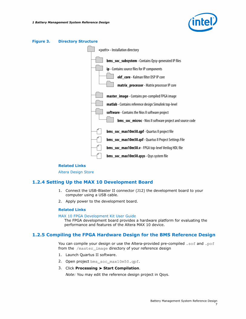
Figure 3. Directory Structure
bms_soc_subsystem - Contains Qysy-generated IP files
<path> - Installation directory
ip - Contains source files for IP components
ekf_core - Kalman filter DSP IP core
matrix_processor - Matrix processor IP core
master_image - Contains pre-compiled FPGA image
matlab - Contains reference design Simulink top-level
software - Contains the Nios II software project
bms_soc_microc - Nios II software project and source code
bms_soc_max10m50.qpf - Quartus II project file
bms_soc_max10m50.qsf - Quartus II Project Settings File
bms_soc_max10m50.v - FPGA top-level Verilog HDL file
bms_soc_max10m50.qsys - Qsys system file
Related Links
Altera Design Store
1.2.4 Setting Up the MAX 10 Development Board
1. Connect the USB-Blaster II connector (J12) the development board to yourcomputer using a USB cable.
2. Apply power to the development board.
Related Links
MAX 10 FPGA Development Kit User GuideThe FPGA development board provides a hardware platform for evaluating theperformance and features of the Altera MAX 10 device.
1.2.5 Compiling the FPGA Hardware Design for the BMS Reference Design
You can compile your design or use the Altera-provided pre-compiled .sof and .poffrom the /master_image directory of your reference design
1. Launch Quartus II software.
2. Open project bms_soc_max10m50.qpf.
3. Click Processing ➤ Start Compilation.
Note: You may edit the reference design project in Qsys.
1 Battery Management System Reference Design
Battery Management System Reference Design7
1.2.6 Compiling the Nios Software for the BMS Reference Design
You can either compile your design or use the Altera-provided pre-compiled .elf fromthe software/ bms_soc_microc directory of your reference design.
1. Start Nios II EDS by clickingStart ➤ Altera ➤ Nios II EDS ➤ Nios II SoftwareBuild Tools
2. Specify the \software folder as the workspace by browsing to the referencedesign /software directory.
3. Click OK to create the workspace.
4. Import application and board support package (BSP) projects:
a. Click File ➤ Import.
b. Expand General and click Existing Projects into Workspace.
c. Click Next.
d. Browse to \software\bms_soc_microc and click OK.
e. Click Finish.
f. Repeat steps a4.a on page 8. to e4.a on page 8. for bms_soc_microc_bsp.
5. Rebuild the BSP project:
a. Right click bms_soc_microc_bsp project
b. Point to Nios II
c. Click Generate BSP
6. Build the application project:
a. Right-click bms_soc_microc project
b. Click Build Project.
Note: On Windows operating systems, the first time you build, the project mighttake up to one hour.
7. Note: build and rebuild the project if you make any changes to the Qsys project.
1.2.7 Programming the BMS Reference Design Hardware onto the Device
1. In the Quartus II software, click Tools ➤ Programmer.
2. In the Programmer pane, select USB-Blaster II under Hardware Setup andJTAG under Mode.
3. Click Auto Detect to detect devices.
4. Select any 10M50 device.
5. Right click 10M50 device, select Edit, and click Change file.
6. Select the output_files/<project_name>.sof or output_files/<projectname>.pof and click Open.
7. Turn on Program/Configure.
8. Click Start.
1 Battery Management System Reference Design
Battery Management System Reference Design8
Note: If you program using .sof file, reprogram the device after removing powerfrom the board. If you program using .pof file, on-chip flash keeps theimage, and you do not need to program the device after removing powerfrom the board. It takes longer to program the device initially usingthe .pof file.
1.2.8 Downloading the BMS Reference Design Nios II Software to theDevice
1. Start Nios II EDS, by clicking Start ➤ Altera ➤ Nios II EDS ➤ Nios IICommand Shell
2. In the command shell, go to the software project folder by entering:cd<reference_design_path>/software/bms_soc_microc
3. In the command shell, download the software by entering: nios2-download -r–g bms_soc_microc.elfWhen the downloadis successful, you see the following message in the terminal:
Using cable “USB-BlasterII on <computername> [USB-1]”, device 1, instance 0x00Resetting and pausing target processor: OKInitializing CPU cache <if present>OKDownloaded 65KB in 0.0sVerified OKStarting Processor at address 0x00000190
4. In the Nios II EDS, click Run ➤ Run configurations... .
5. Double click Nios II Hardware to generate a new run configuration.
6. Click New_configuration.
7. On the Project tab select the bms_soc_microc project in Project name.
8. Turn on Enable browse for file system ELF file.
9. Browse to the software\ bms_soc_microc and select bms_soc_microc.elf.
10. On the Target Connection tab, click Refresh Connections.The software finds the USB-Blaster cable.
11. Click Apply to save changes, optionally specifying a name for the newconfiguration.
12. Click Run to start the software.
13. Check that the terminal console display shows the message:
Start hardware interaction
1.2.9 MATLAB Simulink Top-Level Design for the BMS Reference Design
The reference design uses the Simulink model demo_top.slx, which callssetup_demo_top.m file to initialize all parameters.
1 Battery Management System Reference Design
Battery Management System Reference Design9

Figure 4. Simulink Top-Level Design
The driving cycle block allows you to select the speed profile.
Figure 5. Driving Cycle
The car model block allows you to select the car model parameters.
1 Battery Management System Reference Design
Battery Management System Reference Design10
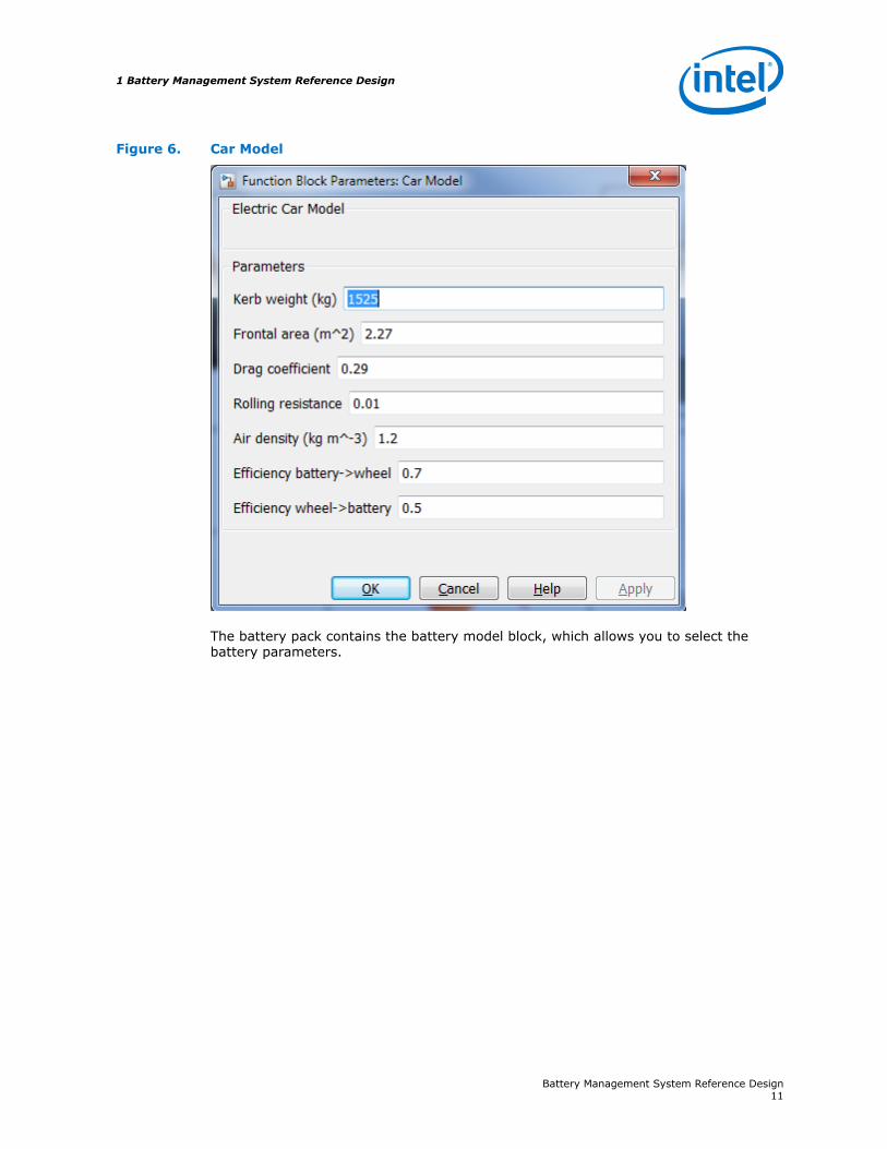
Figure 6. Car Model
The battery pack contains the battery model block, which allows you to select thebattery parameters.
1 Battery Management System Reference Design
Battery Management System Reference Design11
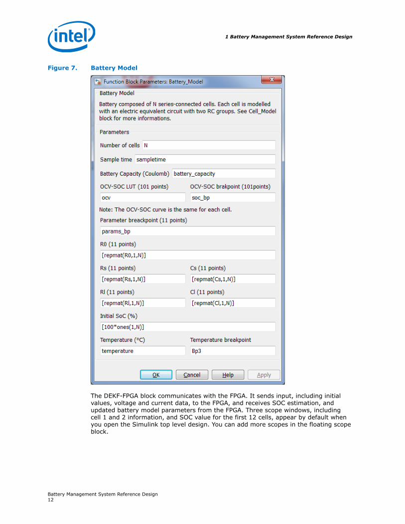
Figure 7. Battery Model
The DEKF-FPGA block communicates with the FPGA. It sends input, including initialvalues, voltage and current data, to the FPGA, and receives SOC estimation, andupdated battery model parameters from the FPGA. Three scope windows, includingcell 1 and 2 information, and SOC value for the first 12 cells, appear by default whenyou open the Simulink top level design. You can add more scopes in the floating scopeblock.
1 Battery Management System Reference Design
Battery Management System Reference Design12
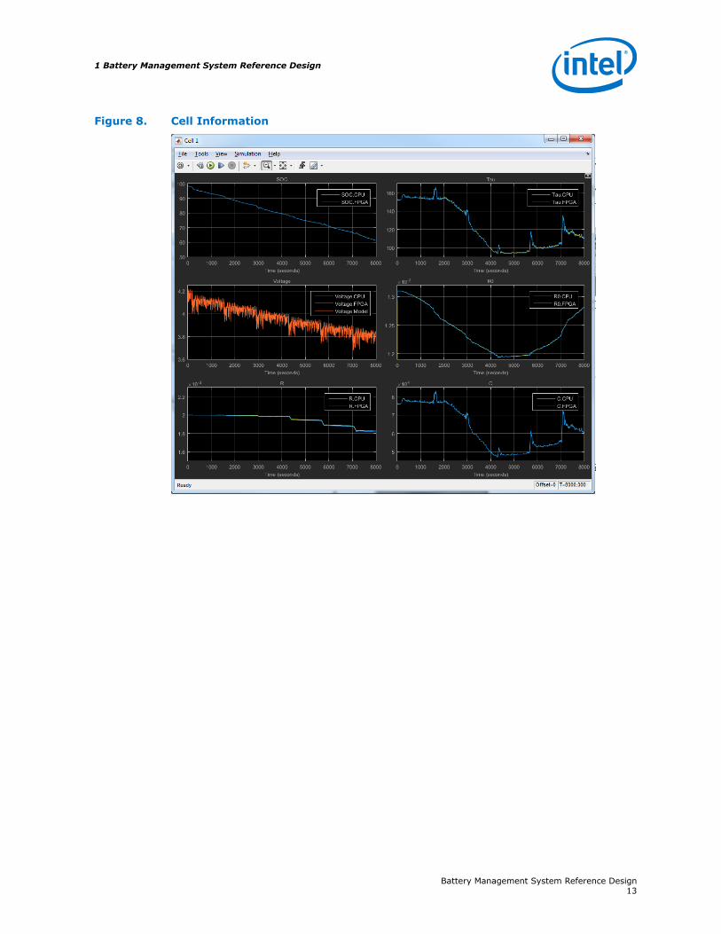
Figure 8. Cell Information
1 Battery Management System Reference Design
Battery Management System Reference Design13
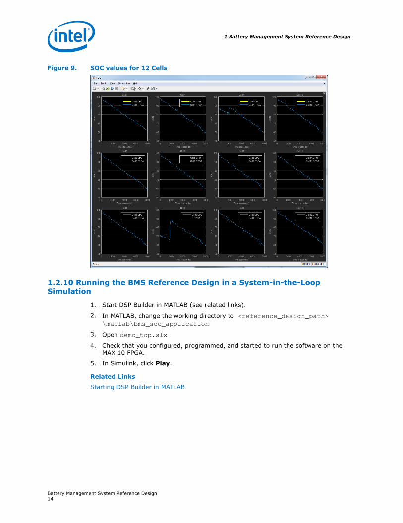
Figure 9. SOC values for 12 Cells
1.2.10 Running the BMS Reference Design in a System-in-the-LoopSimulation
1. Start DSP Builder in MATLAB (see related links).
2. In MATLAB, change the working directory to <reference_design_path>\matlab\bms_soc_application
3. Open demo_top.slx
4. Check that you configured, programmed, and started to run the software on theMAX 10 FPGA.
5. In Simulink, click Play.
Related Links
Starting DSP Builder in MATLAB
1 Battery Management System Reference Design
Battery Management System Reference Design14
1.3 BMS Reference Design Functional Description
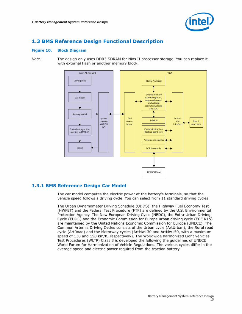
Figure 10. Block Diagram
Note: The design only uses DDR3 SDRAM for Nios II processor storage. You can replace itwith external flash or another memory block.
Equivalent algortihmrunning in MATLAB
Scope
Car model
SystemconsoleMATLAB
API
Battery model
Nios II processor
DDR3 SDRAM
Driving cycle
MATLAB Simulink FPGA
Avalon-MM
Interface
JTAGAvalonbridge
Onchip memory(control registers, measured current
and voltage,estimated voltage
and SOC)
Performance counter
DDR3 controller
Custom instruction floating-point core
Matrix Processor
DEKF IP
1.3.1 BMS Reference Design Car Model
The car model computes the electric power at the battery’s terminals, so that thevehicle speed follows a driving cycle. You can select from 11 standard driving cycles.
The Urban Dynamometer Driving Schedule (UDDS), the Highway Fuel Economy Test(HWFET) and the Federal Test Procedure (FTP) are defined by the U.S. EnvironmentalProtection Agency. The New European Driving Cycle (NEDC), the Extra-Urban DrivingCycle (EUDC) and the Economic Commission for Europe urban driving cycle (ECE R15)are maintained by the United Nations Economic Commission for Europe (UNECE). TheCommon Artemis Driving Cycles consists of the Urban cycle (ArtUrban), the Rural roadcycle (ArtRoad) and the Motorway cycles (ArtMw130 and ArtMw150, with a maximumspeed of 130 and 150 km/h, respectively). The Worldwide harmonized Light vehiclesTest Procedures (WLTP) Class 3 is developed the following the guidelines of UNECEWorld Forum for Harmonization of Vehicle Regulations. The various cycles differ in theaverage speed and electric power required from the traction battery.
1 Battery Management System Reference Design
Battery Management System Reference Design15
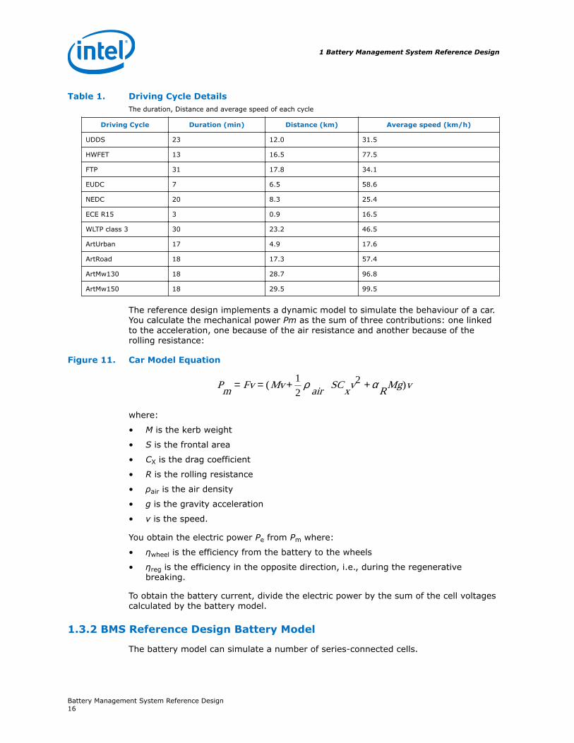
Table 1. Driving Cycle DetailsThe duration, Distance and average speed of each cycle
Driving Cycle Duration (min) Distance (km) Average speed (km/h)
UDDS 23 12.0 31.5
HWFET 13 16.5 77.5
FTP 31 17.8 34.1
EUDC 7 6.5 58.6
NEDC 20 8.3 25.4
ECE R15 3 0.9 16.5
WLTP class 3 30 23.2 46.5
ArtUrban 17 4.9 17.6
ArtRoad 18 17.3 57.4
ArtMw130 18 28.7 96.8
ArtMw150 18 29.5 99.5
The reference design implements a dynamic model to simulate the behaviour of a car.You calculate the mechanical power Pm as the sum of three contributions: one linkedto the acceleration, one because of the air resistance and another because of therolling resistance:
Figure 11. Car Model Equation
vMg
Rv
xSC
airvMFv
mP )2
2
1( αρ ++== �
where:
• M is the kerb weight
• S is the frontal area
• CX is the drag coefficient
• R is the rolling resistance
• ρair is the air density
• g is the gravity acceleration
• v is the speed.
You obtain the electric power Pe from Pm where:
• ηwheel is the efficiency from the battery to the wheels
• ηreg is the efficiency in the opposite direction, i.e., during the regenerativebreaking.
To obtain the battery current, divide the electric power by the sum of the cell voltagescalculated by the battery model.
1.3.2 BMS Reference Design Battery Model
The battery model can simulate a number of series-connected cells.
1 Battery Management System Reference Design
Battery Management System Reference Design16
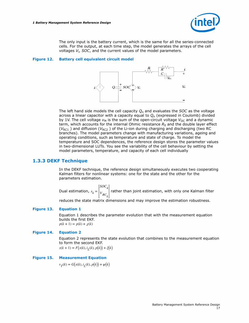
The only input is the battery current, which is the same for all the series-connectedcells. For the output, at each time step, the model generates the arrays of the cellvoltages Vi, SOC, and the current values of the model parameters.
Figure 12. Battery cell equivalent circuit model
-+iL Qn SOC Voc
R0 Ri
Ci
VRCi
iL
+
--
+
VM
The left hand side models the cell capacity Qn and evaluates the SOC as the voltageacross a linear capacitor with a capacity equal to Qn (expressed in Coulomb) dividedby 1V. The cell voltage vM is the sum of the open-circuit voltage VOC and a dynamicterm, which accounts for the internal Ohmic resistance R0 and the double layer effect(VRC1 ) and diffusion (VRC2 ) of the Li-ion during charging and discharging (two RCbranches). The model parameters change with manufacturing variations, ageing andoperating conditions, such as temperature and state of charge. To model thetemperature and SOC dependences, the reference design stores the parameter valuesin two-dimensional LUTs. You see the variability of the cell behaviour by setting themodel parameters, temperature, and capacity of each cell individually
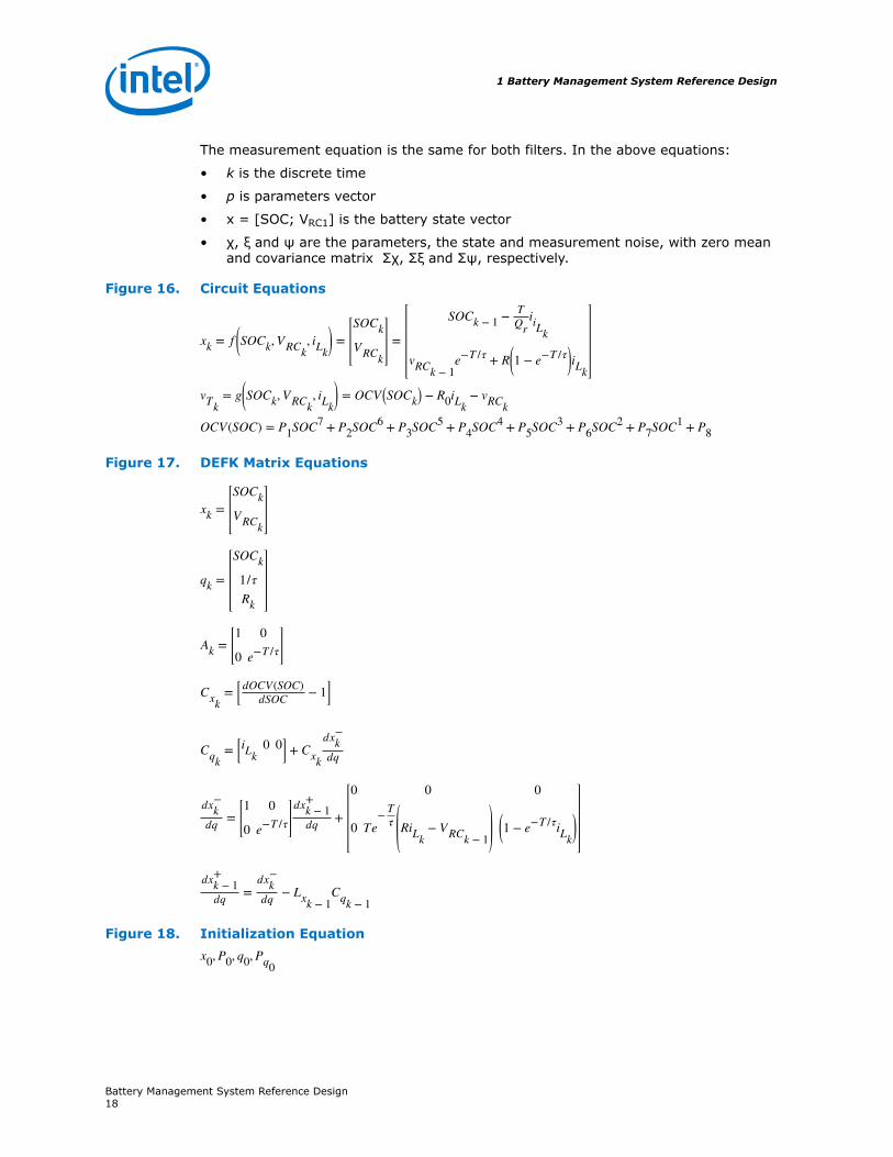
1.3.3 DEKF Technique
In the DEKF technique, the reference design simultaneously executes two cooperatingKalman filters for nonlinear systems: one for the state and the other for theparameters estimation.
Dual estimation, xk =SOCkVRCk
rather than joint estimation, with only one Kalman filter
reduces the state matrix dimensions and may improve the estimation robustness.
Figure 13. Equation 1Equation 1 describes the parameter evolution that with the measurement equationbuilds the first EKF.p k + 1 = p k + χ k
Figure 14. Equation 2Equation 2 represents the state evolution that combines to the measurement equationto form the second EKF.x k + 1 = F x k , iL k , p k + ξ k
Figure 15. Measurement Equation
vT k = G x k , iL k , p k + ψ k
1 Battery Management System Reference Design
Battery Management System Reference Design17
The measurement equation is the same for both filters. In the above equations:
• k is the discrete time
• p is parameters vector
• x = [SOC; VRC1] is the battery state vector
• χ, ξ and ψ are the parameters, the state and measurement noise, with zero meanand covariance matrix Σχ, Σξ and Σψ, respectively.
Figure 16. Circuit Equations
xk = f SOCk, VRCk, iLk
=SOCkVRCk
=
SOCk − 1 − TQr
iiLk
vRCk − 1e−T /τ + R 1 − e−T /τ iLk
vTk= g SOCk, VRCk
, iLk= OCV SOCk − R0iLk
− vRCk
OCV SOC = P1SOC7 + P2SOC6 + P3SOC5 + P4SOC4 + P5SOC3 + P6SOC2 + P7SOC1 + P8
Figure 17. DEFK Matrix Equations
xk =SOCkVRCk
qk =
SOCk1/τRk
Ak =1 0
0 e−T /τ
Cxk= dOCV SOC
dSOC − 1
Cqk= iLk
0 0 + Cxk
dxk−
dq
dxk−
dq =1 0
0 e−T /τdxk − 1
+
dq +
0 0 0
0 Te− T
τ RiLk− VRCk − 1
1 − e−T /τiLk
dxk − 1+
dq =dxk
−
dq − Lxk − 1Cqk − 1
Figure 18. Initialization Equationx0, P0, q0, Pq0
1 Battery Management System Reference Design
Battery Management System Reference Design18
Figure 19. Prediction Equations
qk− = qk − 1
+ Pqk− = Pqk − 1
+ + Qqxk− = f xk − 1
+ , uk − 1, qk − 1+ Pk
− = AkPk − 1+ Ak
T + Q
Figure 20. Correction Equation
Lxk= Pk
−CxkT Cxk
Pk−Cxk
T + R−1
xk+ = xk
− + Lxkyk
− g xk−, uk, qk − 1
+
Pk− = I − Lxk
CxkPk
−
Lqk= Pqk
− CqkT Cqk
Pqk− Cqk
T + R−1
qk+ = qk
+ + Lqkyk
− g xk−, uk, qk − 1
+
Pqk− = I − Lqk
CqkPqk
−
Related Links
R. Morello et al., "Comparison of state and parameter estimators for electric vehiclebatteries," Industrial Electronics Society, IECON 2015 - 41st Annual Conference of theIEEE, Yokohama, 2015, pp. 005433-005438
1.3.4 BMS Reference Design Hardware Implementation
The reference design includes three different designs to implement the DEKFalgorithm:
• Design A,which has a Nios II processor with floating-point acceleration
• Design B, which has a Nios II processor with floating-point acceleration andfloating-point matrix processor
• Design C, which has a Nios II processor and DEKF algorithm implemented indedicated floating-point IP
The reference design creates the dedicated floating-point IP using Altera’s DSP Builderadvanced blockset. In each design, every functional component takes charge ofdifferent tasks, including system-in-the-loop communication with MATLAB Simulink,cell link list management, DEKF calculation. In the three designs, the Nios processor IIcontrols the system-in-the-loop and cell link tasks. In design B, both the Nios IIprocessor and matrix processor perform the DEKF calculation, and the matrixprocessor processes most of the matrix calculations. Finally, in design C, DSP BuilderIP processes all DEKF calculations.
1 Battery Management System Reference Design
Battery Management System Reference Design19
To switch between different implementation methods, modify this line in source file
\software\bms_soc_microc\soc_kalman.h: // 0 - Nios2 only // 1 - Matrix processor // 2 - DSP Builder IP #define ACC 1
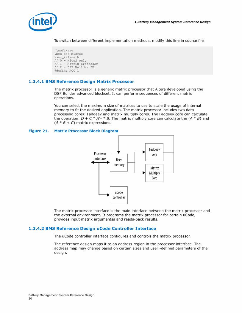
1.3.4.1 BMS Reference Design Matrix Processor
The matrix processor is a generic matrix processor that Altera developed using theDSP Builder advanced blockset. It can perform sequences of different matrixoperations.
You can select the maximum size of matrices to use to scale the usage of internalmemory to fit the desired application. The matrix processor includes two dataprocessing cores: Faddeev and matrix multiply cores. The Faddeev core can calculatethe operation: D + C * A-1 * B. The matrix multiply core can calculate the (A * B) and(A * B + C) matrix expressions.
Figure 21. Matrix Processor Block Diagram
Usermemory
Processorinterface
Faddeevcore
MatrixMultiply
Core
uCodecontroller
The matrix processor interface is the main interface between the matrix processor andthe external environment. It programs the matrix processor for certain uCode,provides input matrix argumentss and reads-back results.
1.3.4.2 BMS Reference Design uCode Controller Interface
The uCode controller interface configures and controls the matrix processor.
The reference design maps it to an address region in the processor interface. Theaddress map may change based on certain sizes and user -defined parameters of thedesign.
1 Battery Management System Reference Design
Battery Management System Reference Design20
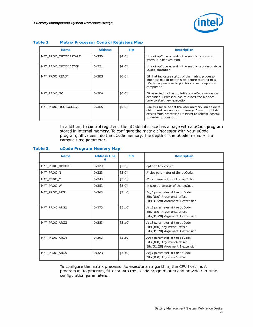
Table 2. Matrix Processor Control Registers Map
Name Address Bits Description
MAT_PROC_OPCODESTART 0x320 [4:0] Line of opCode at which the matrix processorstarts uCode execution.
MAT_PROC_OPCODESTOP 0x321 [4:0] Line of opCode at which the matrix processor stopsuCode execution.
MAT_PROC_READY 0x3B3 [0:0] Bit that indicates status of the matrix processor.The host has to test this bit before starting newuCode sequence or to poll for current sequencecompletion
MAT_PROC_GO 0x3B4 [0:0] Bit asserted by host to initiate a uCode sequenceexecution. Processor has to assert the bit eachtime to start new execution.
MAT_PROC_HOSTACCESS 0x3B5 [0:0] Use this bit to select the user memory multiplex toobtain and release user memory. Assert to obtainaccess from processor. Deassert to release controlto matrix processor.
In addition, to control registers, the uCode interface has a page with a uCode programstored in internal memory. To configure the matrix pProcessor with your uCodeprogram, fill values into the uCode memory. The depth of the uCode memory is acompile-time parameter.
Table 3. uCode Program Memory Map
Name Address Line0
Bits Description
MAT_PROC_OPCODE 0x323 [3:0] opCode to execute.
MAT_PROC_N 0x333 [3:0] N size parameter of the opCode.
MAT_PROC_M 0x343 [3:0] M size parameter of the opCode.
MAT_PROC_W 0x353 [3:0] W size parameter of the opCode.
MAT_PROC_ARG1 0x363 [31:0] Arg1 parameter of the opCodeBits [8:0] Argument1 offsetBits[31:28] Argument 1 extension
MAT_PROC_ARG2 0x373 [31:0] Arg2 parameter of the opCodeBits [8:0] Argument2 offsetBits[31:28] Argument 4 extension
MAT_PROC_ARG3 0x383 [31:0] Arg3 parameter of the opCodeBits [8:0] Argument3 offsetBits[31:28] Argument 4 extension
MAT_PROC_ARG4 0x393 [31:0] Arg4 parameter of the opCodeBits [8:0] Argument4 offsetBits[31:28] Argument 4 extension
MAT_PROC_ARG5 0x3A3 [31:0] Arg5 parameter of the opCodeBits [8:0] Argument5 offset
To configure the matrix processor to execute an algorithm, the CPU host mustprogram it. To program, fill data into the uCode program area and provide run-timeconfiguration parameters.
1 Battery Management System Reference Design
Battery Management System Reference Design21
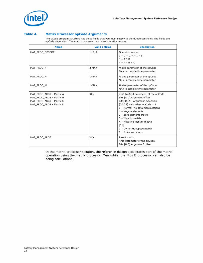
Table 4. Matrix Processor opCode ArgumentsThe uCode program structure has these fields that you must supply to the uCode controller. The fields areopCode dependent. The matrix processor has three operation modes. .
Name Valid Entries Description
MAT_PROC_OPCODE 1, 3, 4 Operation mode:1 – D + C * A-1 * B3 – A * B4 – A * B + C
MAT_PROC_N 2-MAX N size parameter of the opCodeMAX is compile time parameter
MAT_PROC_M 1-MAX M size parameter of the opCodeMAX is compile time parameter
MAT_PROC_W 1-MAX W size parameter of the opCodeMAX is compile time parameter
MAT_PROC_ARG1 – Matrix AMAT_PROC_ARG2 – Matrix BMAT_PROC_ARG3 – Matrix CMAT_PROC_ARG4 – Matrix D
XXX Arg1 to Arg4 parameter of the opCodeBits [8:0] Argument offsetBits[31:28] Argument extension[30:28] Valid when opCode = 10 – Normal (no data manipulation)1 – Negate elements2 – Zero elements Matrix3 – Identity matrix4 – Negative identity matrix[31]0 – Do not transpose matrix1 – Transpose matrix
MAT_PROC_ARG5 XXX Result matrixArg5 parameter of the opCodeBits [8:0] Argument5 offset
In the matrix processor solution, the reference design accelerates part of the matrixoperation using the matrix processor. Meanwhile, the Nios II processor can also bedoing calculations.
1 Battery Management System Reference Design
Battery Management System Reference Design22
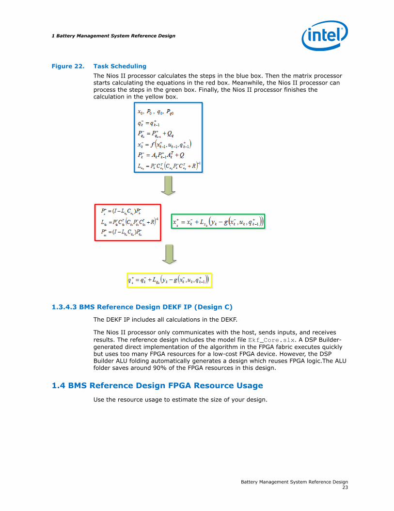
Figure 22. Task SchedulingThe Nios II processor calculates the steps in the blue box. Then the matrix processorstarts calculating the equations in the red box. Meanwhile, the Nios II processor canprocess the steps in the green box. Finally, the Nios II processor finishes thecalculation in the yellow box.
1.3.4.3 BMS Reference Design DEKF IP (Design C)
The DEKF IP includes all calculations in the DEKF.
The Nios II processor only communicates with the host, sends inputs, and receivesresults. The reference design includes the model file Ekf_Core.slx. A DSP Builder-generated direct implementation of the algorithm in the FPGA fabric executes quicklybut uses too many FPGA resources for a low-cost FPGA device. However, the DSPBuilder ALU folding automatically generates a design which reuses FPGA logic.The ALUfolder saves around 90% of the FPGA resources in this design.
1.4 BMS Reference Design FPGA Resource Usage
Use the resource usage to estimate the size of your design.
1 Battery Management System Reference Design
Battery Management System Reference Design23

Table 5. Resource Usage
Component LE M9K DSP
DEKF IP (design C only) 20,610 30 29
Matrix processor (design B only) 6,304 35 24
Nios II processor 2,916 32 6
Nios II floating-point custom instruction core 2,204 3 9
DDR controller 4,785 12 0
Avalon-MM interconnect 5,897 0 0
JTAG-Avalon-MM bridge 799 1 0
Miscellaneous 1,292 23 0
Design A total ~14,000 57 15
Design B total ~24,000 92 39
Design C total ~33,000 84 35
Total ~45,000/50,000 136/182 68
1.5 BMS Reference Design Benchmarking
Table 6. Execution Time for Updating One Cell
Implementation Method Time to Update One Cell (μs)
Design A 44.9
Design B 33.8
Design C 16.5
1.6 Acknowledgements for the BMS Reference Design
Altera wants to acknowledge the help of Federico Baronti of the University of Pisa withthe models and algorithms used in this reference design.
1 Battery Management System Reference Design
Battery Management System Reference Design24