bcm4330 preliminary data sheet - linux-sunxilinux-sunxi.org/images/0/05/4330-ds206-r.pdfpreliminary...
TRANSCRIPT

10/9/2011 7T5YL
Preliminary Data Sheet
BCM4330
4330-DS206-R
5300 California Avenue • Irvine, CA 92617 • Phone: 949-926-5000 • Fax: 949-926-5203 August 17, 2011
Single Chip IEEE 802.11™ a/b/g/n MAC/Baseband/Radio with Integrated Bluetooth® 4.0 + HS and FM
Transceiver
Figure 1: Functional Block Diagram
GENERAL DESCRIPTION FEATURES
The Broadcom® BCM4330 single chip device provides for the highest level of integration for a mobile or handheld wireless system, with integrated IEEE 802.11™ a/b/g and single-stream 802.11n (MAC/baseband/radio), Bluetooth® 4.0 + HS, and FM radio receiver and transmitter. It includes on-chip 2.4 GHz and 5 GHz WLAN CMOS power amplifiers that meet the output power requirements of most handheld systems while permitting an optional external power amplifier for higher output power applications, if required.
Utilizing advanced design techniques and process technology to reduce active and idle power, the BCM4330 is designed to address the needs of highly mobile devices that require minimal power consumption and compact size. It includes a power management unit which simplifies the system power topology and allows for operation directly from a mobile platform battery while maximizing battery life.
The BCM4330 implements the highly sophisticated Enhanced Collaborative Coexistence radio coexistence algorithms and hardware mechanisms, allowing for an extremely collaborative Bluetooth coexistence scheme along with coexistence support for external radios (such as GPS, WiMax, or Ultra Wide-band radio technologies, as well as cellular radios) and a single shared antenna (2.4 GHz antenna for Bluetooth and WLAN). As a result, enhanced overall quality for simultaneous voice, video, and data transmission on a handheld system is achieved.
For the WLAN section, two alternative host interface options are included: an SDIO v2.0 interface that can operate in 4b, 1b, or gSPI modes, and an HSIC interface. An independent, high-speed UART is provided for the Bluetooth host interface. Package options include 4.89 mm x 5.33 mm WLBGA and WLCSP, and 6.5 mm x 6.5 mm FCFBGA.
I2S_DO/PCM_OUT (FM Rx)
I2S_DI/PCM_IN (FM Tx)
I2S_WS/PCM_SYNC (FM Rx/Tx)
I2S_CK/PCM_CLK (FM Rx/Tx)
Analog Audio Out
UART
UART_WAKEUP
BT_WAKEUP
I2S/PCM
UART
BT_RESETx
CLK_REQ
HSIC
SDIO*/SPI
WL_IRQ
WL_RESETx
WLANHost I/F
BluetoothHost I/F
FM TX/RXHost I/F
BCM4330
T/R Switch or FEM
SP3T Switch
5 GHz WLAN Tx
5 GHz WLAN Rx
2.4 GHz WLAN Tx
2.4 GHz WLAN/BT Rx
Bluetooth TxCBF
FM TxFM Rx
VbattVIO

10/9/2011 7T5YL
Revision HistoryBCM4330 Preliminary Data Sheet
BROADCOM August 17, 2011 • 4330-DS206-R Page 2
®
FEATURES FEATURES
IEEE 802.11x Key Features• Single-band 2.4 GHz 802.11 b/g/n or dual-
band 2.4 GHz and 5 GHz 802.11 a/b/g/n (non-simultaneous)
• Single stream 802.11n support for 20 MHz channels provides PHY layer rates up to MCS7 (72 Mbps) for typical upper-layer throughput in excess of 45 Mbps.
• Integrated CMOS power amplifiers with internal power-detectors and closed-loop power control can deliver greater than 18 dBm of linear output power (in 2.4 GHz band).
• PAs can be powered directly from VBAT, eliminating the need for a PALDO.
• Up to 8 RF control signals are available to support optional external PAs for higher output power and LNAs for enhanced sensitivity.
• Supports a single 2.4 GHz antenna shared between WLAN and Bluetooth.
• Shared Bluetooth and WLAN receive signal path eliminates the need for an external power splitter while maintaining excellent sensitivity for both Bluetooth and WLAN.
• Internal fractional nPLL allows support for a wide range of reference clock frequencies
• Supports IEEE 802.15.2 external three-wire coexistence scheme to optimize bandwidth utilization with other co-located wireless technologies such as GPS, WiMax, or UWB
• Supports standard SDIO v2.0 (50 MHz, 4-bit and 1-bit), and gSPI (48 MHz) host interfaces.
• Alternative host interface supports HSIC (a USB 2.0 derivative for short-distance, on-board connections).
• Integrated ARM® Cortex-M3 processor and on-chip memory for complete WLAN subsystem functionality, minimizing the need to wake up the applications processor for standard WLAN functions. This allows for further minimization of power consumption, while maintaining the ability to field upgrade with future features.
• OneDriver™ software architecture for easy migration from existing embedded WLAN and Bluetooth devices as well as future devices.
Bluetooth and FM Key Features• Bluetooth Core Specification Version 4.0 + HS compliant
with provisions for supporting future specifications• Bluetooth Class 1 or Class 2 transmitter operation• Supports extended Synchronous Connections (eSCO), for
enhanced voice quality by allowing for retransmission of dropped packets
• Adaptive Frequency Hopping (AFH) for reducing radio frequency interference
• Interface support — Host Controller Interface (HCI) using a high-speed UART interface and PCM for audio data
• The FM unit supports HCI for communication, stereo analog input and output
• Low-power consumption improves battery life of handheld devices
• FM receiver: 65 MHz to 108 MHz FM bands; supports the European Radio Data Systems (RDS) and the North American Radio Broadcast Data System (RBDS) standards
• Supports multiple simultaneous Advanced Audio Distribution Profiles (A2DP) for stereo sound
• Automatic frequency detection for standard crystal and TCXO values
• FM transmitter: 65 MHz to 108 MHz bands; supports both RDS and the RBDS standards and programmable output power.
General Features• Supports battery voltage range from 2.3V to 4.8V
supplies with internal switching regulator• Programmable dynamic power management• 2 Kbit OTP for storing board parameters • Package options:
- 144 ball FCFBGA (6.5 mm x 6.5 mm, 0.5 mm pitch)- 133 ball WLBGA (4.89 mm x 5.33 mm, 0.4 mm pitch)- 225 bump WLCSP (4.89 mm x 5.33 mm, 0.2 mm
pitch)• Security:
- WPA™- and WPA2™- (Personal) support for powerful encryption and authentication
- AES and TKIP in hardware for faster data encryption and 802.11i compatibility
- Reference WLAN subsystem provides Cisco® Compatible Extension- (CCX, CCX 2.0, CCX 3.0, CCX 4.0, CCX 5.0) certified
- Reference WLAN subsystem provides Wi-Fi Protected Setup (WPS)
• Worldwide regulatory support: Global products supported with worldwide homologated design

10/9/2011 7T5YL
Broadcom®, the pulse logo, Connecting everything®, and the Connecting everything logo are among the trademarks of Broadcom Corporation and/or its affiliates in the United States, certain other countries and/or
the EU. Any other trademarks or trade names mentioned are the property of their respective owners.
This data sheet (including, without limitation, the Broadcom component(s) identified herein) is not designed, intended, or certified for use in any military, nuclear, medical, mass transportation, aviation, navigations,
pollution control, hazardous substances management, or other high-risk application. BROADCOM PROVIDES THIS DATA SHEET “AS-IS,” WITHOUT WARRANTY OF ANY KIND. BROADCOM DISCLAIMS ALL WARRANTIES,
EXPRESSED AND IMPLIED, INCLUDING, WITHOUT LIMITATION, THE IMPLIED WARRANTIES OF MERCHANTABILITY, FITNESS FOR A PARTICULAR PURPOSE, AND NON-INFRINGEMENT.
Broadcom Corporation5300 California Avenue
Irvine, CA 92617
© 2011 by Broadcom CorporationAll rights reserved
Printed in the U.S.A.
Revision History
Revision Date Change Description
4330-DS206-R 8/17/11 Updated:• Table 51: “HSIC Interface Specifications,” on page 156.• Table 54: “Ordering Information,” on page 167.
4330-DS205-R 8/10/11 Updated:• “Voltage Regulators” on page 25.• The introduction of Section 4: “Bluetooth + FM Subsystem Overview,” on
page 37.• Figure 8: “Startup Signaling Sequence,” on page 45.• “FM Radio” on page 65.• Table 18: “FCFBGA, WLBGA, and WLCSP Signal Descriptions,” on
page 104.• Table 19: “WLAN GPIO Functions and Strapping Options,” on page 113.• Table 23: “I/O States,” on page 116.• Table 26: “ESD Specifications,” on page 119.• Table 27: “Recommended Operating Conditions and DC
Characteristics,” on page 120.• Table 31: “FM Transmitter Specifications,” on page 127.• Table 32: “FM Receiver Specifications,” on page 129.• Table 34: “WLAN 2.4 GHz Receiver Performance Specifications,” on
page 135.• Table 35: “WLAN 2.4 GHz Transmitter Performance Specifications,” on
page 138.• Table 36: “WLAN 5 GHz Receiver Performance Specifications,” on
page 140.• Table 37: “WLAN 5 GHz Transmitter Performance Specifications,” on
page 142.• “WLAN Current Consumption” on page 150.• Table 51: “HSIC Interface Specifications,” on page 157.• Figure 49: “WLAN = ON, Bluetooth = OFF,” on page 161.

10/9/2011 7T5YL
Revision HistoryBCM4330 Preliminary Data Sheet
BROADCOM August 17, 2011 • 4330-DS206-R Page 4
®
4330-DS204-R 4/28/11 Updated:• Global change: the maximum voltage for VBAT, VDD_PA, CBUCK, and
LDO3P3, LDO3P1 was changed to 4.8V throughout the document.• “General Features” on page 2• “External 32.768 kHz Low Power Oscillator” on page 36• Table 18: “FCFBGA, WLBGA, and WLCSP Signal Descriptions,” on page
104• Table 19: “WLAN GPIO Functions and Strapping Options,” on page 111• Table 26: “ESD Specifications,” on page 117• Table 27: “Recommended Operating Conditions and DC Characteristics,”
on page 118• Table 31: “FM Transmitter Specifications,” on page 125• Table 32: “FM Receiver Specifications,” on page 127• Table 34: “WLAN 2.4 GHz Receiver Performance Specifications,” on page
133• Table 36: “WLAN 5 GHz Receiver Performance Specifications,” on page
138• Table 39: “Core Buck Regulator (CBUCK) Specifications,” on page 142• Table 40: “LDO3p1 Specifications,” on page 143• Table 41: “LDO3p3 Specifications,” on page 144• Table 42: “CLDO Specifications,” on page 145• Table 43: “LNLDO1 Specifications,” on page 146• Table 46: “Bluetooth and FM Current Consumption,” on page 150Added:• Table 20: “Strap Options,” on page 111 • “HSIC Interface Specifications” on page 155
Revision Date Change Description

10/9/2011 7T5YL
Revision HistoryBCM4330 Preliminary Data Sheet
BROADCOM August 17, 2011 • 4330-DS206-R Page 5
®
4330-DS203-R 1/26/11 Added:• “Bluetooth Low Energy” on page 37.• Table 23: “I/O States,” on page 108.• Table 45: “HSIC Power Consumption,” on page 142.• Figure 51: “WLAN Warm Reset,” on page 153.Updated:• Figure 2: “BCM4330 Block Diagram,” on page 17.• “Power Supply Topology” on page 22.• Figure 4: “Typical Power Topology,” on page 23.• Table 1: “Reset Control Signals,” on page 26.• Figure 7: “Recommended Circuit to Use with an External Shared TCXO,”
on page 28.• “Features” on page 33.• “Bluetooth Radio” on page 35.• “Bluetooth 4.0 Features” on page 37.• Table 4: “Power Control Pin Description,” on page 39.• Figure 8: “Startup Signaling Sequence,” on page 40.• “RAM, ROM, and Patch Memory” on page 46.• “I2S Interface” on page 57.• “Audio Features” on page 62.• “WLAN CPU and Memory Subsystem” on page 66.• “External Coexistence Interface” on page 67.• Figure 34: “WLAN MAC Architecture,” on page 80.• Figure 37: “Radio Functional Block Diagram,” on page 87.• Figure 38: “144-FCFBGA Ball Map (top view),” on page 88.• Figure 39: “133-WLBGA Ball Map (bottom view),” on page 89.• Table 18: “FCFBGA, WLBGA, and WLCSP Signal Descriptions,” on
page 98.• Table 21: “GPIO Multiplexing Matrix,” on page 106.• Table 22: “Multiplexed GPIO Signals,” on page 107.• Table 26: “ESD Specifications,” on page 111.• Table 27: “Recommended Operating Conditions and DC
Characteristics,” on page 112.• Table 28: “Bluetooth Receiver RF Specifications,” on page 115.• Table 29: “Bluetooth Transmitter RF Specifications,” on page 116.• Table 30: “Local Oscillator Performance,” on page 118.• Table 31: “FM Transmitter Specifications,” on page 119.• Table 32: “FM Receiver Specifications,” on page 121.• Figure 42: “FM Receiver Circuit,” on page 125.• Table 34: “WLAN 2.4 GHz Receiver Performance Specifications,” on
page 127.• Table 35: “WLAN 2.4 GHz Transmitter Performance Specifications,” on
page 130.
Revision Date Change Description

10/9/2011 7T5YL
Revision HistoryBCM4330 Preliminary Data Sheet
BROADCOM August 17, 2011 • 4330-DS206-R Page 6
®
4330-DS203-R (continued)
1/26/11 Updated:• Table 39: “Core Buck Regulator (CBUCK) Specifications,” on page 136.• Table 41: “LDO3p3 Specifications,” on page 138.• Table 42: “CLDO Specifications,” on page 138.• Table 43: “LNLDO1 Specifications,” on page 140.• Table 44: “WLAN Power Consumption (Ivbat+Ivio),” on page 141.• Table 46: “Bluetooth and FM Current Consumption,” on page 143.• Figure 53: “133-Ball WLBGA Package Mechanical Information,” on page
156.• “WLCSP Package Keep-Out Area” on page 158.• Table 53: “Ordering Information,” on page 159.Removed:• Section 9: “Enhanced Scanning Algorithm”.
4330-DS202-R 7/1/10 Updated:• Table 34 on page 125.
4330-DS201-R 6/24/10 Added:• Figure 6: “Recommended Circuit to Use with an External Dedicated TCXO,”
on page 26.• Figure 7: “Recommended Circuit to Use with an External Shared TCXO,”
on page 26.• “External 32.768 kHz Low Power Oscillator” on page 30.• Section 6: “Music and Audio,” on page 43.• Figure 37: “WLCSP 225-Bump Map (bottom view),” on page 87.Updated:• Figure 1: “Functional Block Diagram,” on page 1.• Figure 2: “BCM4330 Block Diagram,” on page 15.• “Features” on page 16.• Figure 3: “Mobile Phone Block System Diagram,” on page 19.• “Voltage Regulators” on page 20.• “Reset Circuits” on page 24.• Section 3: “Frequency References,” on page 25.• Table 2: “Crystal Oscillator and External Clock – Requirements and
Performance,” on page 27.• Figure 7: “Recommended Circuit to Use with an External Shared TCXO,”
on page 26.• Table 3: “External 32.768 kHz Sleep Clock Specifications,” on page 30.• “Bluetooth Radio” on page 33.• “Bluetooth Power Management Unit” on page 37.• Figure 8: “Startup Signaling Sequence,” on page 38.• “RAM, ROM, and Patch Memory” on page 44.• “PCM Interface” on page 45.• “UART Interface” on page 53.• “I2S Interface” on page 55.
Revision Date Change Description
10/9/2011 7T5YL
Revision HistoryBCM4330 Preliminary Data Sheet
BROADCOM August 17, 2011 • 4330-DS206-R Page 7
®
4330-DS201-R(continued)
6/24/10 Updated:• Section 10: “FM Transceiver Subsystem,” on page 59.• “GPIO Interface” on page 64.• “JTAG Interface” on page 64.• Figure 35: “144-FCBGA Ball Map (top view),” on page 85.• Figure 36: “133-WLBGA Ball Map (bottom view),” on page 86.• Table 18: “WLCSP 225-Bump Coordinates,” on page 88.• Table 19: “FCBGA, WLBGA, and WLCSP Signal Descriptions,” on page 95.• Table 20: “WLAN GPIO Functions and Strapping Options (Advance
Information),” on page 102.• Table 21: “GPIO Multiplexing Matrix,” on page 103.• Table 22: “Multiplexed GPIO Signals,” on page 104.• Table 23: “Absolute Maximum Ratings,” on page 105.• Table 24: “Environmental Ratings,” on page 106.• Table 26: “Recommended Operating Conditions and DC Characteristics,”
on page 107.• Table 27: “Bluetooth Receiver RF Specifications,” on page 109.• Table 28: “Bluetooth Transmitter RF Specifications,” on page 110.• Table 29: “Local Oscillator Performance,” on page 112.• Table 30: “FM Transmitter Specifications,” on page 113.• Table 31: “FM Receiver Specifications,” on page 116.• Table 33: “WLAN 2.4 GHz Receiver Performance Specifications,” on
page 122.• Table 34: “WLAN 2.4 GHz Transmitter Performance Specifications,” on
page 125.• Table 35: “WLAN 5 GHz Receiver Performance Specifications,” on
page 127.• Table 36: “WLAN 5 GHz Transmitter Performance Specifications,” on
page 129.• Figure 39: “FM Receiver Circuit with External Balun and Cellular Band
Blocking Filter,” on page 120.• Table 38: “Core Buck Regulator (CBUCK) Specifications,” on page 131.• Table 43: “WLAN Power Consumption (Ivbat+Ivio),” on page 135.• Table 44: “Bluetooth and FM Current Consumption,” on page 137.• Figure 49: “133-Ball WLBGA Package Mechanical Information,” on page
148.• Figure 50: “225-Bump WLCSP Package Mechanical Information,” on page
149.• “Ordering Information” on page 150.Removed:• Table 11: “OTP Select,” on page 70.
4330-DS200-R 10/28/09 Initial release.
Revision Date Change Description

10/9/2011 7T5YL
Table of Contents BCM4330 Preliminary Data Sheet
BROADCOM August 17, 2011 • 4330-DS206-R Page 8
®
Table of ContentsAbout This Document...................................................................................................................................18
Purpose and Audience ...........................................................................................................................18
Acronyms and Abbreviations.................................................................................................................18
Document Conventions .........................................................................................................................18
References .............................................................................................................................................19
Technical Support .........................................................................................................................................19
Section 1: BCM4330 Overview......................................................................................... 20
Overview.......................................................................................................................................................20
Features ........................................................................................................................................................21
Standards Compliance..................................................................................................................................22
Mobile Phone Usage Model .........................................................................................................................23
Section 2: Power Supplies and Power Management ........................................................ 24
Power Supply Topology................................................................................................................................24
Voltage Regulators.................................................................................................................................24
WLAN Power Management..........................................................................................................................26
PMU Sequencing ..........................................................................................................................................27
Low-Power Shutdown ..................................................................................................................................28
Reset Circuits ................................................................................................................................................29
Section 3: Frequency References ..................................................................................... 30
Crystal Interface and Clock Generation .......................................................................................................30
TCXO .............................................................................................................................................................31
Frequency Selection .....................................................................................................................................34
External 32.768 kHz Low Power Oscillator ..................................................................................................35
Section 4: Bluetooth + FM Subsystem Overview.............................................................. 36
Features ........................................................................................................................................................36
Bluetooth Radio............................................................................................................................................38
Transmit.................................................................................................................................................38
Digital Modulator...................................................................................................................................38
Digital Demodulator and Bit Synchronizer.............................................................................................38
Power Amplifier .....................................................................................................................................38
Receiver .................................................................................................................................................39
Digital Demodulator and Bit Synchronizer.............................................................................................39
Receiver Signal Strength Indicator.........................................................................................................39
10/9/2011 7T5YL
Table of Contents BCM4330 Preliminary Data Sheet
BROADCOM August 17, 2011 • 4330-DS206-R Page 9
®
Local Oscillator Generation....................................................................................................................39
Calibration..............................................................................................................................................39
Section 5: Bluetooth Baseband Core................................................................................ 40
Bluetooth 4.0 Features .................................................................................................................................40
Bluetooth Low Energy ..................................................................................................................................40
Link Control Layer.........................................................................................................................................41
Test Mode Support.......................................................................................................................................41
Bluetooth Power Management Unit ...........................................................................................................42
RF Power Management .........................................................................................................................42
Host Controller Power Management.....................................................................................................43
BBC Power Management .......................................................................................................................45
FM Power Management ........................................................................................................................45
Low-Power Scan.....................................................................................................................................45
Wideband Speech ..................................................................................................................................45
Packet Loss Concealment ......................................................................................................................46
Audio Rate-Matching Algorithms ..........................................................................................................46
Codec Encoding......................................................................................................................................47
Multiple Simultaneous A2DP Audio Stream ..........................................................................................47
FM Over Bluetooth ................................................................................................................................47
Burst Buffer Operation ..........................................................................................................................47
Adaptive Frequency Hopping.......................................................................................................................47
Advanced Bluetooth/WLAN Coexistence ....................................................................................................48
Fast Connection (Interlaced Page and Inquiry Scans) .................................................................................48
Section 6: Music and Audio ............................................................................................. 49
MP3 Encoder.................................................................................................................................................49
MP3 Decoder ................................................................................................................................................49
AAC/AAC+ Decoder ......................................................................................................................................49
Section 7: Microprocessor and Memory Unit for Bluetooth............................................. 50
RAM, ROM, and Patch Memory...................................................................................................................50
Reset .............................................................................................................................................................50
Section 8: Bluetooth Peripheral Transport Unit ............................................................... 51
PCM Interface ...............................................................................................................................................51
Slot Mapping..........................................................................................................................................51
Frame Synchronization ..........................................................................................................................51
Data Formatting.....................................................................................................................................51

10/9/2011 7T5YL
Table of Contents BCM4330 Preliminary Data Sheet
BROADCOM August 17, 2011 • 4330-DS206-R Page 10
®
Wideband Speech Support ....................................................................................................................52
Multiplexed Bluetooth and FM Over PCM.............................................................................................52
Burst PCM Mode....................................................................................................................................52
PCM Interface Timing ............................................................................................................................53
Short Frame Sync, Master Mode ....................................................................................................53
Short Frame Sync, Slave Mode .......................................................................................................54
Long Frame Sync, Master Mode .....................................................................................................55
Long Frame Sync, Slave Mode ........................................................................................................56
Short Frame Sync, Burst Mode .......................................................................................................57
Long Frame Sync, Burst Mode ........................................................................................................58
UART Interface .............................................................................................................................................59
I2S Interface ..................................................................................................................................................61
I2S Timing ...............................................................................................................................................61
Section 9: FM Transceiver Subsystem.............................................................................. 64
FM Radio .......................................................................................................................................................64
Digital FM Audio Interfaces..........................................................................................................................64
Analog FM Audio Interfaces.........................................................................................................................64
FM Over Bluetooth .......................................................................................................................................64
eSCO..............................................................................................................................................................65
Wide Band Speech Link ................................................................................................................................65
A2DP .............................................................................................................................................................65
Dynamic Antenna Switching ........................................................................................................................65
Autotune and Search Algorithms.................................................................................................................66
Audio Features .............................................................................................................................................66
On-Chip MP3 Encoding.................................................................................................................................68
RDS/RBDS .....................................................................................................................................................69
Section 10: WLAN Global Functions................................................................................. 70
WLAN CPU and Memory Subsystem............................................................................................................70
One-Time-Programmable Memory..............................................................................................................70
GPIO Interface ..............................................................................................................................................71
External Coexistence Interface ....................................................................................................................71
UART Interface .............................................................................................................................................71
JTAG Interface ..............................................................................................................................................71
Section 11: WLAN Host Interfaces ................................................................................... 72
SDIO v2.0 ......................................................................................................................................................72

10/9/2011 7T5YL
Table of Contents BCM4330 Preliminary Data Sheet
BROADCOM August 17, 2011 • 4330-DS206-R Page 11
®
SDIO Pin Descriptions ............................................................................................................................72
Generic SPI Mode .........................................................................................................................................74
SPI Protocol............................................................................................................................................75
Command Structure .......................................................................................................................76
Write...............................................................................................................................................76
Write/Read .....................................................................................................................................76
Read................................................................................................................................................76
Status ..............................................................................................................................................77
gSPI Host-Device Handshake .................................................................................................................79
Boot-Up Sequence .................................................................................................................................79
HSIC Interface ...............................................................................................................................................82
Section 12: Wireless LAN MAC and PHY........................................................................... 83
MAC Features ...............................................................................................................................................83
MAC Description ....................................................................................................................................83
PSM.................................................................................................................................................85
WEP ................................................................................................................................................85
TXE ..................................................................................................................................................86
RXE..................................................................................................................................................86
IFS ...................................................................................................................................................87
TSF ..................................................................................................................................................87
NAV.................................................................................................................................................87
MAC-PHY Interface .........................................................................................................................87
WLAN PHY Description.................................................................................................................................88
PHY Features..........................................................................................................................................88
Section 13: WLAN Radio Subsystem ............................................................................... 91
Receive Path .................................................................................................................................................91
Transmit Path ...............................................................................................................................................91
Calibration ....................................................................................................................................................91
Section 14: Pinout and Signal Descriptions ...................................................................... 93
Signal Assignments .......................................................................................................................................93
WLAN GPIO Signals and Strapping Options .........................................................................................112
Muxed Bluetooth GPIO Signals ............................................................................................................113
I/O States .............................................................................................................................................115
Section 15: DC Characteristics ....................................................................................... 117
Absolute Maximum Ratings .......................................................................................................................117
10/9/2011 7T5YL
Table of Contents BCM4330 Preliminary Data Sheet
BROADCOM August 17, 2011 • 4330-DS206-R Page 12
®
Environmental Ratings ...............................................................................................................................118
Electrostatic Discharge Specifications .......................................................................................................118
Recommended Operating Conditions and DC Characteristics ..................................................................119
Section 16: Bluetooth RF Specifications......................................................................... 121
Section 17: FM Transmitter Specifications ..................................................................... 126
Section 18: FM Receiver Specifications .......................................................................... 128
Section 19: WLAN RF Specifications............................................................................... 133
Introduction................................................................................................................................................133
2.4 GHz Band General RF Specifications ....................................................................................................134
WLAN 2.4 GHz Receiver Performance Specifications ................................................................................134
WLAN 2.4 GHz Transmitter Performance Specifications...........................................................................137
WLAN 5 GHz Receiver Performance Specifications ...................................................................................139
WLAN 5 GHz Transmitter Performance Specifications..............................................................................141
General Spurious Emissions Specifications................................................................................................142
Section 20: Internal Regulator Electrical Specifications.................................................. 143
Core Buck Regulator ...................................................................................................................................143
LDO3p1 .......................................................................................................................................................144
LDO3p3 .......................................................................................................................................................145
CLDO ...........................................................................................................................................................146
LNLDO1 .......................................................................................................................................................147
Section 21: System Power Consumption........................................................................ 148
WLAN Current Consumption......................................................................................................................149
WLAN Current Consumption — 2.4 GHz Operation .............................................................................149
WLAN Current Consumption — 5 GHz Operation ................................................................................150
HSIC Interface Current Consumption.........................................................................................................151
Bluetooth and FM Current Consumption ..................................................................................................151
Section 22: Interface Timing and AC Characteristics ...................................................... 152
SDIO/gSPI Timing........................................................................................................................................152
SDIO Default Mode Timing ..................................................................................................................152
SDIO High-Speed Mode Timing............................................................................................................154
gSPI Signal Timing ................................................................................................................................155
HSIC Interface Specifications......................................................................................................................156
JTAG Timing ................................................................................................................................................157

10/9/2011 7T5YL
Table of Contents BCM4330 Preliminary Data Sheet
BROADCOM August 17, 2011 • 4330-DS206-R Page 13
®
Section 23: Power-Up Sequence and Timing.................................................................. 158
Sequencing of Reset and Regulator Control Signals..................................................................................158
Description of Control Signals..............................................................................................................159
Control Signal Timing Diagrams ...........................................................................................................159
Section 24: Package Information ................................................................................... 162
Package Thermal Characteristics ...............................................................................................................162
Junction Temperature Estimation and PSIJT Versus THETAJC ...................................................................162
Environmental Characteristics ...................................................................................................................162
Section 25: Mechanical Information .............................................................................. 163
WLCSP Package Keep-Out Area .................................................................................................................166
Section 26: Ordering Information .................................................................................. 167
10/9/2011 7T5YL
List of Figures BCM4330 Preliminary Data Sheet
BROADCOM August 17, 2011 • 4330-DS206-R Page 14
®
List of FiguresFigure 1: Functional Block Diagram....................................................................................................................1
Figure 2: BCM4330 Block Diagram ...................................................................................................................20
Figure 3: Mobile Phone Block System Diagram................................................................................................23
Figure 4: Typical Power Topology.....................................................................................................................25
Figure 5: Recommended Oscillator Configuration ...........................................................................................30
Figure 6: Recommended Circuit to Use with an External Dedicated TCXO......................................................31
Figure 7: Recommended Circuit to Use with an External Shared TCXO...........................................................31
Figure 8: Startup Signaling Sequence ...............................................................................................................44
Figure 9: CVSD Decoder Output Waveform Without PLC ................................................................................46
Figure 10: CVSD Decoder Output Waveform After Applying PLC ....................................................................46
Figure 11: Functional Multiplex Data Diagram.................................................................................................52
Figure 12: PCM Timing Diagram (Short Frame Sync, Master Mode)................................................................53
Figure 13: PCM Timing Diagram (Short Frame Sync, Slave Mode)...................................................................54
Figure 14: PCM Timing Diagram (Long Frame Sync, Master Mode).................................................................55
Figure 15: PCM Timing Diagram (Long Frame Sync, Slave Mode)....................................................................56
Figure 16: PCM Burst Mode Timing (Receive Only, Short Frame Sync) ...........................................................57
Figure 17: PCM Burst Mode Timing (Receive Only, Long Frame Sync) ............................................................58
Figure 18: UART Timing ....................................................................................................................................60
Figure 19: I2S Transmitter Timing.....................................................................................................................63
Figure 20: I2S Receiver Timing..........................................................................................................................63
Figure 21: Example Blend/Switch Usage ..........................................................................................................67
Figure 22: Example Blend/Switch Separation ..................................................................................................67
Figure 23: Example Soft Mute Characteristic ...................................................................................................68
Figure 24: Signal Connections to SDIO Host (SD 4-Bit Mode) ..........................................................................73
Figure 25: Signal Connections to SDIO Host (SD 1-Bit Mode) ..........................................................................73
Figure 26: Signal Connections to SDIO Host (gSPI Mode) ................................................................................74
Figure 27: gSPI Write Protocol .........................................................................................................................75
Figure 28: gSPI Read Protocol ..........................................................................................................................75
Figure 29: gSPI Command Structure.................................................................................................................76
Figure 30: gSPI Signal Timing Without Status...................................................................................................77
Figure 31: gSPI Signal Timing with Status (Response Delay = 0) ......................................................................78
Figure 32: WLAN Boot-Up Sequence................................................................................................................81
Figure 33: HSIC Device Block Diagram..............................................................................................................82
Figure 34: WLAN MAC Architecture .................................................................................................................84
Figure 35: WLAN PHY Block Diagram ...............................................................................................................89

10/9/2011 7T5YL
List of Figures BCM4330 Preliminary Data Sheet
BROADCOM August 17, 2011 • 4330-DS206-R Page 15
®
Figure 36: STBC Receive Block Diagram ...........................................................................................................90
Figure 37: Radio Functional Block Diagram......................................................................................................92
Figure 38: 144-FCFBGA Ball Map (Top View) ...................................................................................................93
Figure 39: 133-WLBGA Ball Map (bottom view) ..............................................................................................94
Figure 40: WLCSP 225-Bump Map (bottom view)............................................................................................95
Figure 41: RF Port Location for Bluetooth Testing .........................................................................................121
Figure 42: FM Receiver Circuit .......................................................................................................................132
Figure 43: Port Locations................................................................................................................................133
Figure 44: SDIO Bus Timing (Default Mode)...................................................................................................152
Figure 45: SDIO Bus Timing (High-Speed Mode) ............................................................................................154
Figure 46: gSPI Timing ....................................................................................................................................155
Figure 47: WLAN = ON, Bluetooth = ON.........................................................................................................159
Figure 48: WLAN = OFF, Bluetooth = OFF.......................................................................................................160
Figure 49: WLAN = ON, Bluetooth = OFF........................................................................................................160
Figure 50: WLAN = OFF, Bluetooth = ON........................................................................................................161
Figure 51: WLAN Warm Reset........................................................................................................................161
Figure 52: 144-Ball FCFBGA Package Mechanical Information ......................................................................163
Figure 53: 133-Ball WLBGA Package Mechanical Information.......................................................................164
Figure 54: 225-Bump WLCSP Package Mechanical Information ....................................................................165
Figure 55: WLCSP Package Keep-outs ............................................................................................................166

10/9/2011 7T5YL
List of Tables BCM4330 Preliminary Data Sheet
BROADCOM August 17, 2011 • 4330-DS206-R Page 16
®
List of TablesTable 1: Reset Control Signals ..........................................................................................................................29
Table 2: Crystal Oscillator and External Clock – Requirements and Performance ...........................................32
Table 3: External 32.768 kHz Sleep Clock Specifications..................................................................................35
Table 4: Power Control Pin Descriptions ..........................................................................................................43
Table 5: PCM Interface Timing Specifications (Short Frame Sync, Master Mode)...........................................53
Table 6: PCM Interface Timing Specifications (Short Frame Sync, Slave Mode) ..............................................54
Table 7: PCM Interface Timing Specifications (Long Frame Sync, Master Mode)............................................55
Table 8: PCM Interface Timing Specifications (Long Frame Sync, Slave Mode) ...............................................56
Table 9: PCM Burst Mode (Receive Only, Short Frame Sync) ..........................................................................57
Table 10: PCM Burst Mode (Receive Only, Long Frame Sync) .........................................................................58
Table 11: Example of Common Baud Rates......................................................................................................59
Table 12: UART Timing Specifications ..............................................................................................................60
Table 13: Timing for I2S Transmitters and Receivers........................................................................................62
Table 14: SDIO Pin Description.........................................................................................................................72
Table 15: gSPI Status Field Details....................................................................................................................78
Table 16: gSPI Registers....................................................................................................................................79
Table 17: WLCSP 225-Bump Coordinates.........................................................................................................96
Table 18: FCFBGA, WLBGA, and WLCSP Signal Descriptions..........................................................................103
Table 19: WLAN GPIO Functions and Strapping Options ...............................................................................112
Table 20: Strap Options..................................................................................................................................112
Table 21: GPIO Multiplexing Matrix ...............................................................................................................113
Table 22: Multiplexed GPIO Signals................................................................................................................114
Table 23: I/O States ........................................................................................................................................115
Table 24: Absolute Maximum Ratings............................................................................................................117
Table 25: Environmental Ratings....................................................................................................................118
Table 26: ESD Specifications...........................................................................................................................118
Table 27: Recommended Operating Conditions and DC Characteristics .......................................................119
Table 28: Bluetooth Receiver RF Specifications .............................................................................................122
Table 29: Bluetooth Transmitter RF Specifications ........................................................................................123
Table 30: Local Oscillator Performance..........................................................................................................125
Table 31: FM Transmitter Specifications........................................................................................................126
Table 32: FM Receiver Specifications .............................................................................................................128
Table 33: 2.4 GHz Band General RF Specifications.........................................................................................134
Table 34: WLAN 2.4 GHz Receiver Performance Specifications .....................................................................134
Table 35: WLAN 2.4 GHz Transmitter Performance Specifications................................................................137

10/9/2011 7T5YL
List of Tables BCM4330 Preliminary Data Sheet
BROADCOM August 17, 2011 • 4330-DS206-R Page 17
®
Table 36: WLAN 5 GHz Receiver Performance Specifications ........................................................................139
Table 37: WLAN 5 GHz Transmitter Performance Specifications...................................................................141
Table 38: General Spurious Emissions Specifications.....................................................................................142
Table 39: Core Buck Regulator (CBUCK) Specifications..................................................................................143
Table 40: LDO3p1 Specifications ....................................................................................................................144
Table 41: LDO3p3 Specifications ....................................................................................................................145
Table 42: CLDO Specifications ........................................................................................................................146
Table 43: LNLDO1 Specifications ....................................................................................................................147
Table 44: WLAN Current Consumption (Ivbat + Ivio)—2.4 GHz Operation....................................................149
Table 45: WLAN Current Consumption (Ivbat + Ivio) — 5 GHz Operation ......................................................150
Table 46: HSIC Interface Current Consumption .............................................................................................151
Table 47: Bluetooth and FM Current Consumption .......................................................................................151
Table 48: SDIO Bus Timing Parameters (Default Mode) ................................................................................153
Table 49: SDIO Bus Timing Parameters (High-Speed Mode)..........................................................................154
Table 50: gSPI Timing Parameters ..................................................................................................................155
Table 51: HSIC Interface Specifications ..........................................................................................................156
Table 52: JTAG Timing Characteristics............................................................................................................157
Table 53: Package Thermal Characteristics ....................................................................................................162
Table 54: Ordering Information .....................................................................................................................167

10/9/2011 7T5YL
About This Document
BROADCOM August 17, 2011 • 4330-DS206-R Page 18
®
BCM4330 Preliminary Data Sheet
About This Document
Purpose and AudienceThis document provides details of the functional, operational, and electrical characteristics of the Broadcom® BCM4330. It is intended for hardware design, application, and OEM engineers.
Acronyms and AbbreviationsIn most cases, acronyms and abbreviations are defined on first use.
For a comprehensive list of acronyms and other terms used in Broadcom documents, go to: http://www.broadcom.com/press/glossary.php.
Document ConventionsThe following conventions may be used in this document:
Convention Description
Bold User input and actions: for example, type exit, click OK, press Alt+CMonospace Code: #include <iostream>
HTML: <td rowspan = 3> Command line commands and parameters: wl [-l] <command>
< > Placeholders for required elements: enter your <username> or wl <command>
[ ] Indicates optional command-line parameters: wl [-l]Indicates bit and byte ranges (inclusive): [0:3] or [7:0]
10/9/2011 7T5YL
Technical Support
BROADCOM August 17, 2011 • 4330-DS206-R Page 19
®
BCM4330 Preliminary Data Sheet
ReferencesThe references in this section may be used in conjunction with this document.
For Broadcom documents, replace the “xx” in the document number with the largest number available in the repository to ensure that you have the most current version of the document.
Technical SupportBroadcom provides customer access to a wide range of information, including technical documentation, schematic diagrams, product bill of materials, PCB layout information, and software updates through its customer support portal (https://support.broadcom.com). For a CSP account, contact your Sales or Engineering support representative.
In addition, Broadcom provides other product support through its Downloads & Support site (http://www.broadcom.com/support/).
Note: Broadcom provides customer access to technical documentation and software through its Customer Support Portal (CSP) and Downloads & Support site (see Technical Support).
Document (or Item) Name Number Source
Broadcom Items
[1] Printed Circuit Board Layout Guidelines and Component Selection for Optimized PMU Performance
4330_4336_AN1xx-R CSP
10/9/2011 7T5YL
BCM4330 Overview
BROADCOM August 17, 2011 • 4330-DS206-R Page 20
®
BCM4330 Preliminary Data Sheet
Section 1: BCM4330 Overview
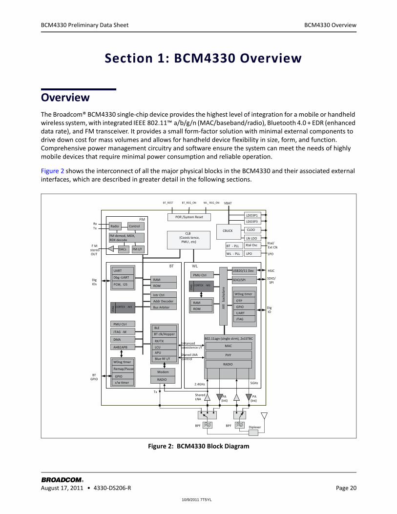
OverviewThe Broadcom® BCM4330 single-chip device provides the highest level of integration for a mobile or handheld wireless system, with integrated IEEE 802.11™ a/b/g/n (MAC/baseband/radio), Bluetooth 4.0 + EDR (enhanced data rate), and FM transceiver. It provides a small form-factor solution with minimal external components to drive down cost for mass volumes and allows for handheld device flexibility in size, form, and function. Comprehensive power management circuitry and software ensure the system can meet the needs of highly mobile devices that require minimal power consumption and reliable operation.
Figure 2 shows the interconnect of all the major physical blocks in the BCM4330 and their associated external interfaces, which are described in greater detail in the following sections.
Figure 2: BCM4330 Block Diagram
PCM, I2S
AHB2APB
AXI
bac
kpla
ne
MAC
PHY
RADIO
Xtal Osc
LPO
GPIO
UART
JTAG
RAM
ROM CORTEX -M3
RAM
ROM
RADIO
Dbg-UART
UART
Shared LNA control
Intr Ctrl
Addr Decoder
Bus Arbiter
WDog mer
GPIO
Remap/Pause
USB20/11 Dev
PMU Ctrl
CLB (Coexis tence,
PMU , etc) BT - PLL
PMU Ctrl
DMA
Shared LNA
LDO3P3
Modem
LCU
Blue RF i/f
APU
s/w mer
JTAG -M
JTA
G
CLDO
LN LDO
RX/TX
BT clk/Hopper
DACs FM I/F
FM demod, MDX, RDX decode
Control Radio Rx
5GHz 2.4GHz
PA (Int)
PA (Int)
BPF BPF Diplexer
F M stereo OUT
BT GPIO
Dig IO
Dig IOs
802.11agn (single strm), 2x1STBC
Xtal/ Ext Clk
Tx
Tx
CORTEX -M3
JTA
G
OTP
WDog mer
Enhanced coexistence i/f
WL - PLL
HSIC
SDIO/SPI SDIO/ SPI
CBUCK
POR /System Reset
BLE
LDO3P1
LPO
VBAT WL_ REG_ON BT_REG_ON BT_REST
FM
BT WL

10/9/2011 7T5YL
Features
BROADCOM August 17, 2011 • 4330-DS206-R Page 21
®
BCM4330 Preliminary Data Sheet
FeaturesThe BCM4330 supports the following features:
• 802.11a/b/g/n dual-band radio — non-simultaneous dual-band operation
• Bluetooth v4.0 + EDR with integrated Class 1 PA
• Concurrent Bluetooth, FM (RX) RDS/RBDS, and WLAN operation
• On-chip WLAN driver execution capable of supporting 802.11 functionality
• Single- and dual-antenna support
– Single antenna without external switch (shared LNA)
– Simultaneous BT/WLAN receive with single antenna
– Support for a 2×1 dual receiver system
• WLAN host interface options:
– SDIO v1.2x (1-bit/4-bit) — up to 50 MHz clock rate
– gSPI — up to 48 MHz clock rate
– HSIC (USB device interface for short distance on-board applications)
• BT host digital interface (can be used concurrently with above interfaces):
– UART (up to 4 Mbps)
• ECI — enhanced coexistence support, ability to coordinate BT SCO transmissions around WLAN receives
• I2S/PCM for FM/BT audio, HCI for FM block control
• HCI high-speed UART (H4, H4+, H5) transport support
• Wideband speech support (16 bits linear data, MSB first, left justified at 4K samples/s for transparent air coding, both through I2S and PCM interface)
• Bluetooth SmartAudio technology improves voice and music quality to headsets
• Bluetooth low power inquiry and page scan
• Bluetooth Low Energy (BLE) support
• Bluetooth Packet Loss Concealment (PLC)
• Bluetooth Wide Band Speech (WBS)
• FM advanced internal antenna support
• FM auto search/tuning functions
• FM multiple audio routing options: I2S, PCM, eSCO, A2DP
• FM mono-stereo blend and switch, and soft mute support
• FM audio pause detect support
• Audio rate-matching algorithms
• Multiple simultaneous A2DP audio stream
• FM over Bluetooth operation and on-chip stereo headset emulation (SBC, MP3, and AAC+)
• MP3, AAC+ on-chip decoder for low power music playback

10/9/2011 7T5YL
Standards Compliance
BROADCOM August 17, 2011 • 4330-DS206-R Page 22
®
BCM4330 Preliminary Data Sheet
Standards ComplianceThe BCM4330 supports the following standards:• Bluetooth 2.1 + EDR• Bluetooth 3.0 + HS• Bluetooth 4.0 (Bluetooth Low Energy)• 65 MHz to 108 MHz FM bands (US, Europe, and Japan) • IEEE 802.11n — Handheld Device Class (Section 11)• 802.11a• 802.11b• 802.11g• 802.11d • 802.11h• 802.11i
The BCM4330 will support the following future drafts/standards:• 802.11r — Fast Roaming (between APs)• 802.11k — resource management• 802.11w — Secure Management Frames• 802.11 Extensions:
– 802.11e QoS Enhancements (as per the WMM® specification is already supported)– 802.11h 5 GHz Extensions– 802.11i MAC Enhancements– 802.11r Fast Roaming Support– 802.11k Radio Resource Measurement
• Security:– WEP– WPA™ Personal – WPA2™ Personal– WMM– WMM-PS (U-APSD)– WMM-SA– AES (Hardware Accelerator)– TKIP (HW Accelerator)– CKIP (SW Support)
• Proprietary Protocols:– CCXv2– CCXv3– CCXv4– CCXv5– WFAEC
• 802.15.2 Coexistence Compliance — on silicon solution compliant with IEEE 3 wire requirements

10/9/2011 7T5YL
Mobile Phone Usage Model
BROADCOM August 17, 2011 • 4330-DS206-R Page 23
®
BCM4330 Preliminary Data Sheet
Mobile Phone Usage ModelThe BCM4330 incorporates a number of unique features to simplify integration into mobile phone platforms. Its flexible PCM and UART interfaces enable it to transparently connect with the existing circuits. In addition, the TCXO and LPO inputs allow the use of existing handset features to further minimize the size, power, and cost of the complete system.
• The PCM interface provides multiple modes of operation to support both master and slave as well as hybrid interfacing to single or multiple external codec devices.
• The UART interface supports hardware flow control with tight integration to power control sideband signaling to support the lowest power operation.
• The TCXO interface accommodates any of the typical reference frequencies used by cell phones.
• An analog FM receiver interface is available for legacy systems.
• FM digital interfaces can use either I2S or PCM.
• The highly linear design of the radio transceiver ensures that the device has the lowest spurious emissions output regardless of the state of operation. It has been fully characterized in the global cellular bands.
• The transceiver design has excellent blocking (eliminating desensitization of the Bluetooth receiver) and intermodulation performance (distortion of the transmitted signal caused by the mixing of the cellular and Bluetooth transmissions) in the presence of a any cellular transmission (GSM®, GPRS, CDMA, WCDMA, or iDEN). Minimal external filtering is required for integration inside the handset.
The BCM4330 is designed to provide direct interface with new and existing handset designs as shown in Figure 3.
Figure 3: Mobile Phone Block System Diagram
T/R Switch or FEM
SP3T Switch
VIO Vbatt
5 GHz WLAN Tx
5 GHz WLAN Rx
2.4 GHz WLAN Tx
2.4 GHz WLAN/BT Rx
Bluetooth Tx
FM Rx
BCM4330
WLAN Host I/F
BluetoothHost I/F
FM Tx/Rx Host I/F
WL_RESETx
SDIO*/SPI
WL_IRQ
BT_RESETx
UART
BT_WAKEUP
UART_WAKEUP
CBFI2S/PCM
FM Tx
CLK_REQ
UART
I2S_DO/PCM_OUT (FM Rx)
Analog Audio Out
I2S_DI/PCM_IN (FM Tx)
I2S_WS/PCM_SYNC (FM Rx/Tx)
I2S_CK/PCM_CLK (FM Rx/Tx)
HSIC

10/9/2011 7T5YL
Power Supplies and Power Management
BROADCOM August 17, 2011 • 4330-DS206-R Page 24
®
BCM4330 Preliminary Data Sheet
Section 2: Power Supplies and Power Management
Power Supply TopologyOne Buck regulator, four LDO regulators, and a Power Management Unit (PMU) are integrated into the BCM4330. All regulators are programmable via the PMU. These blocks simplify power supply design for Bluetooth, WLAN, and FM functions in embedded designs. All regulator inputs and outputs are brought out to pins on the BCM4330. This allows maximum flexibility for the system designer to choose which of the BCM4330 integrated regulators to use.
A single host power supply can be used (including VBATT ranging from 2.3V to 4.8V) with all additional voltages being provided by the regulators in the BCM4330.
Two control signals, BT_REG_ON and WL_REG_ON, are used to power-up the regulators. The CBuck CLDO and LNLDO power up when any of the reset signals are de-asserted. All regulators are powered down only when both resets are asserted. The CLDO and LNLDO may be turned off/on based on the dynamic demands of the digital baseband.
Voltage RegulatorsAll BCM4330 regulator output voltages are PMU-programmable and have the following nominal ratings. The currents listed below indicate the capabilities of each regulator. See Section 21: “System Power Consumption,” on page 148 for the actual operating loads.
• Core Buck switching regulator (CBUCK): 2.3 – 4.8V in; nominal 1.5V, up to 500 mA out
• LDO3p1: 2.3 – 4.8V in; nominal 3.1V, up to 80 mA out
• LDO3p3: 2.3 – 4.8 in; nominal 3.3V, up to 80 mA out
• CLDO (for the core): 1.5V in; nominal 1.2V, up to 150 mA out
• Low-noise LNLDO1: 1.5V in; nominal 1.2V, up to 300 mA out

10/9/2011 7T5YL
Power Supply Topology
BROADCOM August 17, 2011 • 4330-DS206-R Page 25
®
BCM4330 Preliminary Data Sheet
Figure 4 shows the typical power topology.
Figure 4: Typical Power Topology
WL RadioRF PLL
WL AFE
BT Radio
Xtal
FM Radio
Core logic blocks
WL OTP (1.2V)
BT Digital
FM Digital
Noi
se s
ensi
tive
Not
noi
se s
ensi
tive
WL Digital
Internal WLAN PAs
LN LDO1(1.2V, 300 mA)
WL OTP(3.3V)
CLDO(1.2V, 150 mA)
Core Buck Regulator
(1.5V, 500 mA)WL_REG_ON
BT_REG_ON
Vbat 2.3—4.8V
LDO3p3(3.3V, 80 mA)
LDO3p1(3.1V, 80 mA)
WL_VDDIO* and BT_VDDIO*VIO
Notes:
Shaded areas are internal to the BCM4330
RF Switch Controls
BT Class 1 PA
* VDDIO, including WL_VDDIO and BT_VDDIO tied together, low state shuts down all PMU, and VDDIO is detected as high by the PMU if it falls within 1.08— 3.6V.

10/9/2011 7T5YL
WLAN Power Management
BROADCOM August 17, 2011 • 4330-DS206-R Page 26
®
BCM4330 Preliminary Data Sheet
WLAN Power ManagementThe BCM4330 has been designed with the stringent power consumption requirements of mobile devices in mind. All areas of the chip design are optimized to minimize power consumption. Silicon processes and cell libraries were chosen to reduce leakage current and supply voltages. Additionally, the BCM4330 integrated RAM is a high Vt memory with dynamic clock control. The dominant supply current consumed by the RAM is leakage current only. Additionally, the BCM4330 includes an advanced WLAN power management unit (PMU) sequencer. The PMU sequencer provides significant power savings by putting the BCM4330 into various power management states appropriate to the current environment and activities that are being performed. The power management unit enables and disables internal regulators, switches, and other blocks based on a computation of the required resources and a table that describes the relationship between resources and the time needed to enable and disable them. Power up sequences are fully programmable. Configurable, free-running counters (running from the 32.768 kHz LPO clock) in the PMU sequencer are used to turn on/turn off individual regulators and power switches. Clock speeds are dynamically changed (or gated off) based on the instantaneous requirements of the system. Slower clock speeds are used wherever possible.
The BCM4330 WLAN power states are described as follows:
• Active mode — All components in the BCM4330 are powered up and fully functional with active carrier sensing and frame transmission and receiving. All required regulators are enabled and put in the most efficient mode (PWM or Burst) based on the load current. Clock speeds are dynamically adjusted by the PMU sequencer.
• Doze mode — The radio, analog front end (AFE), PLLs, and the ROMs are powered down. The rest of the BCM4330 remains powered up in an IDLE state. All main clocks are shut down. The 32.768 kHz LPO clock is available only for the PMU sequencer. This condition is necessary to allow the PMU sequencer to wake up the chip and transition to Active mode. In Doze mode, the primary power consumed is due to leakage current. The external switcher and internal baseband switcher are put into Burst mode (for better efficiency at low load currents).
• Power-down mode — The BCM4330 is effectively powered off by shutting down all internal regulators. The chip is brought out of this mode by external logic re-enabling the internal regulators.
10/9/2011 7T5YL
PMU Sequencing
BROADCOM August 17, 2011 • 4330-DS206-R Page 27
®
BCM4330 Preliminary Data Sheet
PMU SequencingThe PMU sequencer is responsible for minimizing system power consumption. It enables and disables various system resources based on a computation of the required resources and a table that describes the relationship between resources and the time needed to enable and disable them.
Resource requests may come from several sources: clock requests from cores, the minimum resources defined in the ResourceMin register, and the resources requested by any active resource request timers. The PMU sequencer maps clock requests into a set of resources required to produce the requested clocks.
Each resource is in one of four states: enabled, disabled, transition_on, and transition_off and has a timer that contains 0 when the resource is enabled or disabled and a non-zero value in the transition states. The timer is loaded with the resource's time_on or time_off value when the PMU determines that the resource must be enabled or disabled. That timer decrements on each 32.768 kHz PMU clock. When it reaches 0, the state changes from transition_off to disabled or transition_on to enabled. If the time_on value is 0, the resource can go immediately from disabled to enabled. Similarly, a time_off value of 0 indicates that the resource can go immediately from enabled to disabled. The terms enable sequence and disable sequence refer to either the immediate transition or the timer load-decrement sequence.
During each clock cycle, the PMU sequencer performs the following actions:
1. Computes the required resource set based on requests and the resource dependency table.
2. Decrements all timers whose values are non zero. If a timer reaches 0, the PMU clears the ResourcePending bit for the resource and inverts the ResourceState bit.
3. Compares the request with the current resource status and determines which resources must be enabled or disabled.
4. Initiates a disable sequence for each resource that is enabled, no longer being requested, and has no powered up dependents.
5. Initiates an enable sequence for each resource that is disabled, is being requested, and has all of its dependencies enabled.

10/9/2011 7T5YL
Low-Power Shutdown
BROADCOM August 17, 2011 • 4330-DS206-R Page 28
®
BCM4330 Preliminary Data Sheet
Low-Power ShutdownThe BCM4330 provides a low-power shutdown feature that allows the device to be turned off while the host, and any other devices in the system, remain operational. When the BCM4330 is not needed in the system, VDDRF and VDDC are shut down while VDDO remains powered. This allows the BCM4330 to be effectively off while keeping the I/O pins powered so that they do not draw extra current from any other devices connected to the I/O.
During a low-power shut-down state, provided VDDO remains applied to the BCM4330, all outputs are tristated, and most inputs signals are disabled. Input voltages must remain within the limits defined for normal operation. This is done to prevent current paths or create loading on any digital signals in the system, and enables the BCM4330 to be fully integrated in an embedded device and take full advantage of the lowest power-savings modes.
Two signals on the BCM4330, the frequency reference input (WRF_XTAL_ON) and the LPO input, are designed to be high-impedance inputs that do not load down the driving signal even if the chip does not have VDDO power applied to it.
When the BCM4330 is powered on from this state, it is the same as a normal power-up and the device does not contain any information about its state from before it was powered down.

10/9/2011 7T5YL
Reset Circuits
BROADCOM August 17, 2011 • 4330-DS206-R Page 29
®
BCM4330 Preliminary Data Sheet
Reset CircuitsThe BCM4330 has three signals (see Table 1) that enable or disable the Bluetooth and WLAN circuits and the internal regulator blocks, allowing the host to control power consumption. For timing diagrams of these signals and the required power-up sequences, see Section 23: “Power-Up Sequence and Timing,” on page 158.
In addition, two other input signals control PMU modes:
• When EXT_SMPS_REQ is pulled high, it forces CBUCK to stay on, even when the other regulators are shut down by WL_REG_ON or BT_REG_ON.
• When WLAN and/or Bluetooth are out of reset and EXT_SMPS_REQ is high, then pulling EXT_PWM_REQ high makes CBUCK go into PWM mode, even if internal settings from WLAN and/or Bluetooth are requesting burst mode. During such contention, the request for the higher-power mode wins.
Table 1: Reset Control Signals
Signal Description
WL_REG_ON This signal is used by the PMU (with BT_REG_ON) to power up the WLAN section. It is also OR-gated with the BT_REG_ON input to control the internal BCM4330 regulators. When this pin is high, the regulators are enabled and the WLAN section is out of reset. When this pin is low, the WLAN section is in reset. If BT_REG_ON and WL_REG_ON are both low, the regulators are disabled. Logic High Level: 1.08V–3.6V. 200k pull-down resistor included.
BT_REG_ON This signal is used by the PMU (with WL_REG_ON) to decide whether or not to power down the internal BCM4330 regulators. If BT_REG_ON and WL_REG_ON are low, the regulators will be disabled. Logic High Level: 1.08V–3.6V. 200k pull-down resistor included.
BT_RST_N Low asserting reset for the Bluetooth core. This pin has no effect on WLAN and does not control any PMU functions. It must be driven high or low (not left floating).

10/9/2011 7T5YL
Frequency References
BROADCOM August 17, 2011 • 4330-DS206-R Page 30
®
BCM4330 Preliminary Data Sheet
Section 3: Frequency References
An external crystal is used for generating all radio frequencies and normal operation clocking. As an alternative, an external frequency reference driven by a temperature-compensated crystal oscillator (TCXO) signal may be used. In addition, a low-power oscillator (LPO) is provided for lower power mode timing.
Crystal Interface and Clock GenerationThe BCM4330 can use an external crystal to provide a frequency reference. The recommended configuration for the crystal oscillator including all external components is shown in Figure 5. Consult the reference schematics for the latest configuration.
Figure 5: Recommended Oscillator Configuration
A fractional-N synthesizer in the BCM4330 generates the radio frequencies, clocks, and data/packet timing, enabling it to operate using a wide selection of frequency references.
For SDIO applications the default frequency reference is a 37.4 MHz crystal or TCXO. For HSIC applications, the recommended frequency reference is also 37.4 MHz. The signal characteristics for the crystal interface are listed in Table 2 on page 32.
Note: The crystal and TCXO implementations have different power supplies (WRF_XTAL_VDD1P2 for crystal, WRF_TCXO_VDD for TCXO).
Note: The fractional-N synthesizer can support many reference frequencies. However, frequencies other than the default require support to be added in the driver plus additional, extensive system testing. Contact Broadcom for further details.
12 – 27 pF
12 – 27 pF
WRF_XTAL_ON
WRF_XTAL_OP
C
C
X Ohms*
* Resistor value determined by crystal drive level. See reference schematics for details.
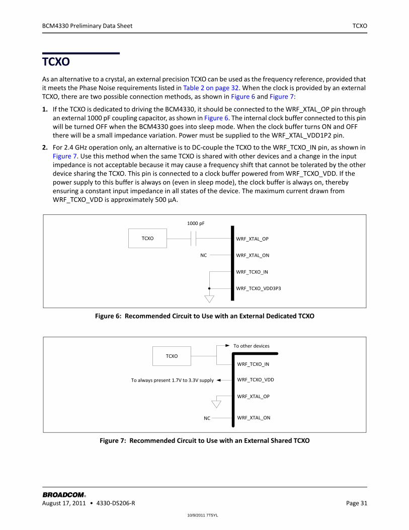
10/9/2011 7T5YL
TCXO
BROADCOM August 17, 2011 • 4330-DS206-R Page 31
®
BCM4330 Preliminary Data Sheet
TCXOAs an alternative to a crystal, an external precision TCXO can be used as the frequency reference, provided that it meets the Phase Noise requirements listed in Table 2 on page 32. When the clock is provided by an external TCXO, there are two possible connection methods, as shown in Figure 6 and Figure 7:
1. If the TCXO is dedicated to driving the BCM4330, it should be connected to the WRF_XTAL_OP pin through an external 1000 pF coupling capacitor, as shown in Figure 6. The internal clock buffer connected to this pin will be turned OFF when the BCM4330 goes into sleep mode. When the clock buffer turns ON and OFF there will be a small impedance variation. Power must be supplied to the WRF_XTAL_VDD1P2 pin.
2. For 2.4 GHz operation only, an alternative is to DC-couple the TCXO to the WRF_TCXO_IN pin, as shown in Figure 7. Use this method when the same TCXO is shared with other devices and a change in the input impedance is not acceptable because it may cause a frequency shift that cannot be tolerated by the other device sharing the TCXO. This pin is connected to a clock buffer powered from WRF_TCXO_VDD. If the power supply to this buffer is always on (even in sleep mode), the clock buffer is always on, thereby ensuring a constant input impedance in all states of the device. The maximum current drawn from WRF_TCXO_VDD is approximately 500 µA.
Figure 6: Recommended Circuit to Use with an External Dedicated TCXO
Figure 7: Recommended Circuit to Use with an External Shared TCXO
TCXO
NC
1000 pF
WRF_XTAL_OP
WRF_XTAL_ON
WRF_TCXO_IN
WRF_TCXO_VDD3P3
TCXO
NC
WRF_TCXO_IN
WRF_XTAL_ON
WRF_XTAL_OP
To other devices
WRF_TCXO_VDDTo always present 1.7V to 3.3V supply
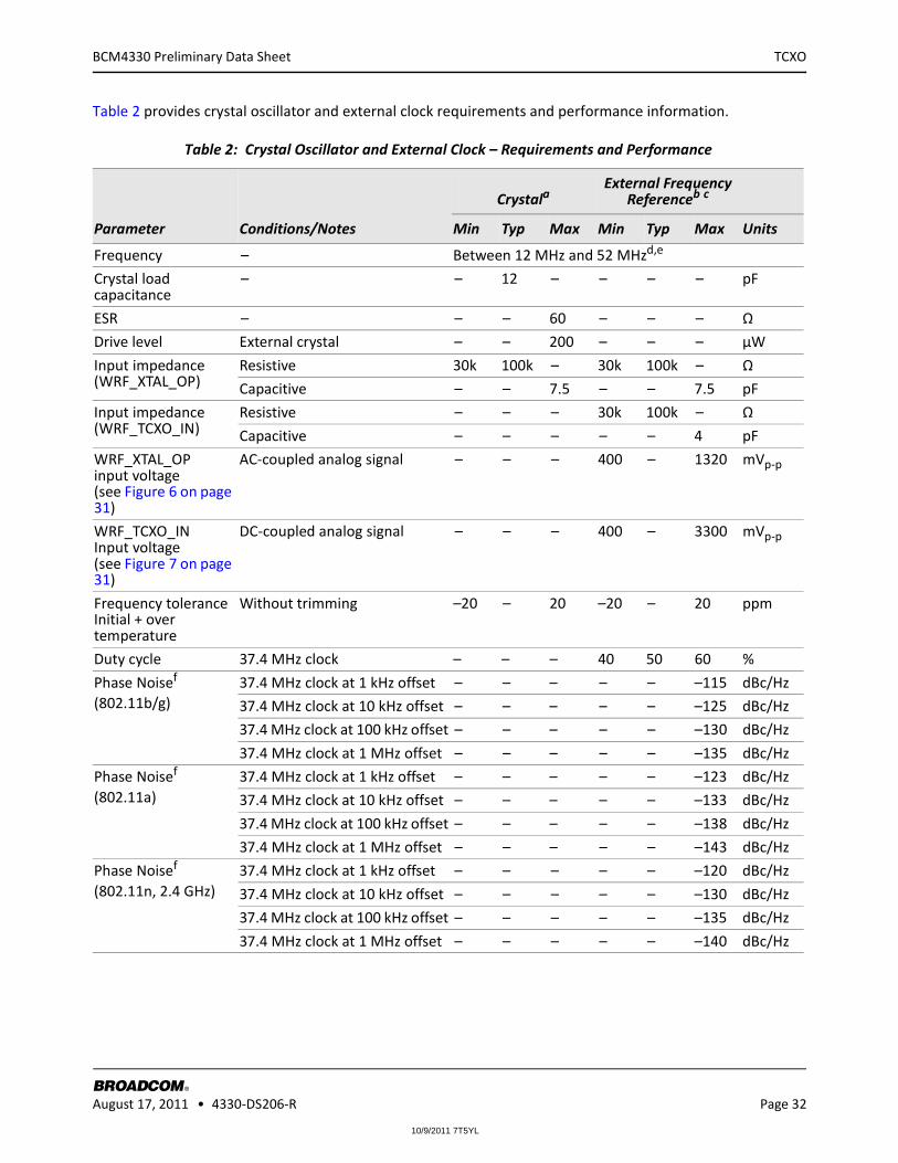
10/9/2011 7T5YL
TCXO
BROADCOM August 17, 2011 • 4330-DS206-R Page 32
®
BCM4330 Preliminary Data Sheet
Table 2 provides crystal oscillator and external clock requirements and performance information.
Table 2: Crystal Oscillator and External Clock – Requirements and Performance
Parameter Conditions/Notes
CrystalaExternal Frequency
Referenceb c
Min Typ Max Min Typ Max Units
Frequency – Between 12 MHz and 52 MHzd,e
Crystal load capacitance
– – 12 – – – – pF
ESR – – – 60 – – – Ω
Drive level External crystal – – 200 – – – µW
Input impedance (WRF_XTAL_OP)
Resistive 30k 100k – 30k 100k – Ω
Capacitive – – 7.5 – – 7.5 pF
Input impedance (WRF_TCXO_IN)
Resistive – – – 30k 100k – Ω
Capacitive – – – – – 4 pF
WRF_XTAL_OP input voltage (see Figure 6 on page 31)
AC-coupled analog signal – – – 400 – 1320 mVp-p
WRF_TCXO_IN Input voltage (see Figure 7 on page 31)
DC-coupled analog signal – – – 400 – 3300 mVp-p
Frequency tolerance Initial + over temperature
Without trimming –20 – 20 –20 – 20 ppm
Duty cycle 37.4 MHz clock – – – 40 50 60 %
Phase Noisef (802.11b/g)
37.4 MHz clock at 1 kHz offset – – – – – –115 dBc/Hz
37.4 MHz clock at 10 kHz offset – – – – – –125 dBc/Hz
37.4 MHz clock at 100 kHz offset – – – – – –130 dBc/Hz
37.4 MHz clock at 1 MHz offset – – – – – –135 dBc/Hz
Phase Noisef
(802.11a)37.4 MHz clock at 1 kHz offset – – – – – –123 dBc/Hz
37.4 MHz clock at 10 kHz offset – – – – – –133 dBc/Hz
37.4 MHz clock at 100 kHz offset – – – – – –138 dBc/Hz
37.4 MHz clock at 1 MHz offset – – – – – –143 dBc/Hz
Phase Noisef
(802.11n, 2.4 GHz)37.4 MHz clock at 1 kHz offset – – – – – –120 dBc/Hz
37.4 MHz clock at 10 kHz offset – – – – – –130 dBc/Hz
37.4 MHz clock at 100 kHz offset – – – – – –135 dBc/Hz
37.4 MHz clock at 1 MHz offset – – – – – –140 dBc/Hz
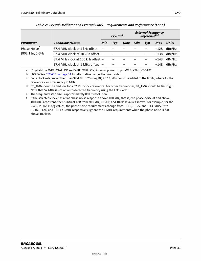
10/9/2011 7T5YL
TCXO
BROADCOM August 17, 2011 • 4330-DS206-R Page 33
®
BCM4330 Preliminary Data Sheet
Phase Noisef
(802.11n, 5 GHz)37.4 MHz clock at 1 kHz offset – – – – – –128 dBc/Hz
37.4 MHz clock at 10 kHz offset – – – – – –138 dBc/Hz
37.4 MHz clock at 100 kHz offset – – – – – –143 dBc/Hz
37.4 MHz clock at 1 MHz offset – – – – – –148 dBc/Hz
a. (Crystal) Use WRF_XTAL_OP and WRF_XTAL_ON, internal power to pin WRF_XTAL_VDD1P2.b. (TCXO) See “TCXO” on page 31 for alternative connection methods.c. For a clock reference other than 37.4 MHz, 20 × log10(f/ 37.4) dB should be added to the limits, where f = the
reference clock frequency in MHz.d. BT_TM6 should be tied low for a 52 MHz clock reference. For other frequencies, BT_TM6 should be tied high.
Note that 52 MHz is not an auto-detected frequency using the LPO clock.e. The frequency step size is approximately 80 Hz resolution.f. If the selected clock has a flat phase noise response above 100 kHz, that is, the phase noise at and above
100 kHz is constant, then subtract 1dB from all 1 kHz, 10 kHz, and 100 kHz values shown. For example, for the 2.4 GHz 802.11b/g values, the phase noise requirements change from – 115, – 125, and – 130 dBc/Hz to – 116, – 126, and – 131 dBc/Hz respectively. Ignore the 1 MHz requirements when the phase noise is flat above 100 kHz.
Table 2: Crystal Oscillator and External Clock – Requirements and Performance (Cont.)
Parameter Conditions/Notes
CrystalaExternal Frequency
Referenceb c
Min Typ Max Min Typ Max Units

10/9/2011 7T5YL
Frequency Selection
BROADCOM August 17, 2011 • 4330-DS206-R Page 34
®
BCM4330 Preliminary Data Sheet
Frequency SelectionAny frequency within the ranges specified for the crystal and TCXO reference may be used. These include not only the standard handset reference frequencies of 12, 13, 14.4, 16.2, 16.8, 19.2, 19.44, 19.68, 19.8, 20, 26, 37.4, and 52 MHz, but also other frequencies in this range, with approximately 80 Hz resolution. The BCM4330 must have the reference frequency set correctly in order for any of the UART or PCM interfaces to function correctly, since all bit timing is derived from the reference frequency.
The reference frequency for the BCM4330 may be set in the following ways:
• Set the “xtalfreq=xxxxx” parameter in the nvram.txt file (used to load the driver) to correctly match the crystal frequency.
• Auto-detect any of the standard handset reference frequencies using an external LPO clock.
For applications such as handsets and portable smart communication devices, where the reference frequency is one of the standard frequencies commonly used, the BCM4330 automatically detects the reference frequency and programs itself to the correct reference frequency. In order for auto frequency detection to work correctly, the BCM4330 must have a valid and stable 32.768 kHz LPO clock that meets the requirements listed in Table 3 on page 35 and is present during power-on reset.
Note: The fractional-N synthesizer can support many reference frequencies. However, frequencies other than the default require support to be added in the driver plus additional, extensive system testing. Contact Broadcom for further details.

10/9/2011 7T5YL
External 32.768 kHz Low Power Oscillator
BROADCOM August 17, 2011 • 4330-DS206-R Page 35
®
BCM4330 Preliminary Data Sheet
External 32.768 kHz Low Power OscillatorThe BCM4330 uses a secondary low frequency clock for low power mode timing.
A precision external 32.768 kHz clock that meets the specifications listed in Table 3 is required by the BCM4330.
Table 3: External 32.768 kHz Sleep Clock Specifications
Parameter LPO Clock Units
Nominal input frequency 32.768 kHz
Frequency accuracy ±200a, b
a. If FM RX is used: ±150 ppm maximum with frequency error indication, ±50 ppm without frequency error indication.
b. If FM TX is used: ±100 ppm maximum with frequency error indication, ±50 ppm without frequency error indication.
ppm
Duty cycle 30 – 70 %
Input signal amplitude 200–1800c
c. 200–1800 mVp-p to avoid additional current consumption and degradation in FM SNR. 3.3 Vp-p maximum.
mV, p-p
Signal type Square-wave or sine-wave –
Input impedanced
d. When power is applied or switched off.
>100k<5
ΩpF
Clock jitter (integrated over 300 Hz–15 kHz) <5 ns
Clock jitter (during initial start-up) <10,000 ppm

10/9/2011 7T5YL
Bluetooth + FM Subsystem Overview
BROADCOM August 17, 2011 • 4330-DS206-R Page 36
®
BCM4330 Preliminary Data Sheet
Section 4: Bluetooth + FM Subsystem Overview
The Broadcom BCM4330 is a Bluetooth 4.0 + EDR-compliant, baseband processor/ 2.4 GHz transceiver with an integrated FM/ RDS/RBDS receiver and FM/RDS transmitter. It features the highest level of integration and eliminates all critical external components, thus minimizing the footprint, power consumption, and system cost of a Bluetooth plus FM radio solution.
The BCM4330 is the optimal solution for any Bluetooth voice and/or data application that also requires an FM radio receiver and transmitter. The Bluetooth subsystem presents a standard Host Controller Interface (HCI) via a high speed UART and PCM for audio. The FM subsystem supports the HCI control interface, analog output, as well as I2S and PCM interfaces. The BCM4330 incorporates all Bluetooth 4.0 features including Secure Simple Pairing, Sniff Subrating, and Encryption Pause and Resume.
The BCM4330 Bluetooth radio transceiver provides enhanced radio performance to meet the most stringent mobile phone temperature applications and the tightest integration into mobile handsets and portable devices. It is fully compatible with any of the standard TCXO frequencies and provides full radio compatibility to operate simultaneously with GPS, WLAN, and cellular radios.
The Bluetooth transmitter also features a Class 1 power amplifier with Class 2 capability.
FeaturesMajor Bluetooth features of the BCM4330 include:
• Supports key features of upcoming Bluetooth standards
• Fully supports Bluetooth Core Specification version 4.0 + (Enhanced Data Rate) EDR features:
– Adaptive Frequency Hopping (AFH)
– Quality of Service (QoS)
– Extended Synchronous Connections (eSCO) — Voice Connections
– Fast Connect (interlaced page and inquiry scans)
– Secure Simple Pairing (SSP)
– Sniff Subrating (SSR)
– Encryption Pause Resume (EPR)
– Extended Inquiry Response (EIR)
– Link Supervision Timeout (LST)
• UART baud rates up to 4 Mbps
• Supports all Bluetooth 4.0 + HS packet types
• Supports maximum Bluetooth data rates over HCI UART
• Multipoint operation with up to seven active slaves
– Maximum of seven simultaneous active ACL links
– Maximum of three simultaneous active SCO and eSCO connections with scatternet support
10/9/2011 7T5YL
Features
BROADCOM August 17, 2011 • 4330-DS206-R Page 37
®
BCM4330 Preliminary Data Sheet
• Narrowband and wideband packet loss concealment
• Scatternet operation with up to four active piconets with background scan and support for scatter mode
• High-speed HCI UART transport support with low-power out-of-band BT_WAKE and HOST_WAKE signaling (see “Host Controller Power Management” on page 43)
• Channel quality driven data rate and packet type selection
• Standard Bluetooth test modes
• Extended radio and production test mode features
• Full support for power savings modes
– Bluetooth clock request
– Bluetooth standard sniff
– Deep-sleep modes and software regulator shutdown
• TCXO input and auto-detection of all standard handset clock frequencies. Also supports a low-power crystal, which can be used during power save mode for better timing accuracy.
Major FM Radio features include:
• 65 MHz to 108 MHz FM bands supported (US, Europe, and Japan)
• FM subsystem control using the Bluetooth HCI interface
• FM subsystem operates from 32.768 kHz low-power oscillator (LPO) or reference clock inputs
• Improved audio interface capabilities with full-featured bidirectional PCM, I2S, and analog stereo DAC
• I2S can be master or slave
FM Receiver-Specific Features Include:
• Excellent FM radio performance with 1 µV sensitivity for 26 dB (S+N)/N
• Signal-dependent stereo/mono blending
• Signal dependent soft mute
• Auto search and tuning modes
• Audio silence detection
• RSSI, IF frequency, status indicators
• RDS and RBDS demodulator and decoder with filter and buffering functions
• Automatic frequency jump
FM Transmitter-Specific Features Include:
• Programmable output power with +120 dBµV maximum output power and 24 dB range
• RDS and RBDS encoder and modulator with intelligent frame encoding and programmable scroll rate
• Programmable audio swing to FM modulation deviation
• Programmable mono or stereo transmission
• Concurrent Bluetooth v4.0 + EDR and FM transmit functionality
• Digital audio input from I2S or PCM
• Host programmable frequency from 76 MHz to 108 MHz in 50 kHz channel steps
• Digitally programmable audio level and mute control
10/9/2011 7T5YL
Bluetooth Radio
BROADCOM August 17, 2011 • 4330-DS206-R Page 38
®
BCM4330 Preliminary Data Sheet
Bluetooth RadioThe BCM4330 has an integrated radio transceiver that has been optimized for use in 2.4 GHz Bluetooth wireless systems. It has been designed to provide low-power, low-cost, robust communications for applications operating in the globally available 2.4 GHz unlicensed ISM band. It is fully compliant with the Bluetooth Radio Specification and EDR specification and meets or exceeds the requirements to provide the highest communication link quality of service.
TransmitThe BCM4330 features a fully integrated zero-IF transmitter. The baseband transmit data is GFSK-modulated in the modem block and upconverted to the 2.4 GHz ISM band in the transmitter path. The transmitter path consists of signal filtering, I/Q upconversion, output power amplifier, and RF filtering. The transmitter path also incorporates π/4 – DQPSK for 2 Mbps and 8 – DPSK for 3 Mbps to support EDR. The transmitter section is compatible to the Bluetooth Low Energy specification. The transmitter PA bias can also be adjusted to provide Bluetooth Class 1 operation.
Digital ModulatorThe digital modulator performs the data modulation and filtering required for the GFSK, π/4 – DQPSK, and 8 – DPSK signal. The fully digital modulator minimizes any frequency drift or anomalies in the modulation characteristics of the transmitted signal and is much more stable than direct VCO modulation schemes.
Digital Demodulator and Bit Synchronizer The digital demodulator and bit synchronizer take the low-IF received signal and perform an optimal frequency tracking and bit-synchronization algorithm.
Power AmplifierThe fully integrated PA supports Class 1 or Class 2 output using a highly linearized, temperature-compensated design. This provides greater flexibility in front-end matching and filtering. The fully integrated PA supports Class 1 and Class 2 output using a temperature-compensated, auto-transformer-based design. This provides a simplified front end that does not require off-chip components for matching and better efficiency. External filtering is required for meeting Bluetooth and regulatory harmonic and spurious requirements. For integrated mobile handset applications where the Bluetooth is integrated next to the cellular radio, minimal external filtering can be applied to achieve near thermal noise levels for spurious and radiated noise emissions. The transmitter features a sophisticated on-chip transmit signal strength indicator (TSSI) block to keep the absolute output power variation within a tight range across process, voltage, and temperature.
10/9/2011 7T5YL
Bluetooth Radio
BROADCOM August 17, 2011 • 4330-DS206-R Page 39
®
BCM4330 Preliminary Data Sheet
Receiver The receiver path uses a low-IF scheme to downconvert the received signal for demodulation in the digital demodulator and bit synchronizer. The receiver path provides a high degree of linearity, an extended dynamic range, and high-order on-chip channel filtering to ensure reliable operation in the noisy 2.4 GHz ISM band. The front-end topology with built-in out-of-band attenuation enables the BCM4330 to be used in most applications with no off-chip filtering. For integrated handset operation, where the Bluetooth function is integrated close to the cellular transmitter, minimal external filtering is required to eliminate the desensitization of the receiver by the cellular transmit signal.
Digital Demodulator and Bit SynchronizerThe digital demodulator and bit synchronizer take the low-IF received signal and perform an optimal frequency tracking and bit synchronization algorithm.
Receiver Signal Strength IndicatorThe radio portion of the BCM4330 provides a Receiver Signal Strength Indicator (RSSI) signal to the baseband, so that the controller can take part in a Bluetooth power-controlled link by providing a metric of its own receiver signal strength to determine whether the transmitter should increase or decrease its output power.
Local Oscillator GenerationLocal Oscillator (LO) generation provides fast frequency hopping (1600 hops/second) across the 79 maximum available channels. The LO generation subblock employs an architecture for high immunity to LO pulling during PA operation. The BCM4330 uses an internal RF and IF loop filter.
CalibrationThe BCM4330 radio transceiver features an automated calibration scheme that is fully self contained in the radio. No user interaction is required during normal operation or during manufacturing to provide the optimal performance. Calibration optimizes the performance of all the major blocks within the radio to optimal conditions, including gain and phase characteristics of filters, matching between key components, and key gain blocks. This takes into account process variation and temperature variation. Calibration occurs transparently during normal operation during the settling time of the hops and calibrates for temperature variations as the device cools and heats during normal operation in its environment.

10/9/2011 7T5YL
Bluetooth Baseband Core
BROADCOM August 17, 2011 • 4330-DS206-R Page 40
®
BCM4330 Preliminary Data Sheet
Section 5: Bluetooth Baseband Core
The Bluetooth Baseband Core (BBC) implements all of the time critical functions required for high-performance Bluetooth operation. The BBC manages the buffering, segmentation, and routing of data for all connections. It also buffers data that passes through it, handles data flow control, schedules SCO/ACL TX/RX transactions, monitors Bluetooth slot usage, optimally segments and packages data into baseband packets, manages connection status indicators, and composes and decodes HCI packets. In addition to these functions, it independently handles HCI event types, and HCI command types.
The following transmit and receive functions are also implemented in the BBC hardware to increase reliability and security of the TX/RX data before sending over the air:
• Symbol timing recovery, data deframing, forward error correction (FEC), header error control (HEC), cyclic redundancy check (CRC), data decryption, and data dewhitening in the receiver.
• Data framing, FEC generation, HEC generation, CRC generation, key generation, data encryption, and data whitening in the transmitter.
Bluetooth 4.0 FeaturesThe BBC supports Bluetooth 4.0 features with the following benefits:
• Dual mode Bluetooth Low Energy (BT and BLE operation).
• Extended Inquiry Response (EIR): Shortens the time to retrieve the device name, specific profile, and operating mode.
• Encryption Pause Resume (EPR): Enables the use of Bluetooth technology in a much more secure environment.
• Sniff Subrating (SSR): Optimizes power consumption for low duty cycle asymmetrical data flow, which subsequently extends battery lifetime.
• Secure Simple Pairing (SSP): Reduces the number of steps for connecting two devices with minimal or no user interaction required.
• Link Supervision Time Out (LSTO): Additional commands added to HCI and Link Management Protocol (LMP) for improved link time-out supervision.
• QoS Enhancements: Changes to data traffic control, which results in better link performance. Audio, human interface design (HID), bulk traffic, SCO and enhanced SCO (eSCO) are improved with the erroneous data (ED) and packet boundary flag (PBF) enhancements.
Bluetooth Low EnergyThe BCM4330 is forward-compatible with the impending Bluetooth Low Energy operating mode, which provides a dramatic reduction in the power consumption of the Bluetooth radio and baseband. The primary application for this mode is to provide support for low data rate devices, such as sensors and remote controls.
10/9/2011 7T5YL
Link Control Layer
BROADCOM August 17, 2011 • 4330-DS206-R Page 41
®
BCM4330 Preliminary Data Sheet
Link Control LayerThe link control layer is part of the Bluetooth link control functions that are implemented in dedicated logic in the link control unit (LCU). This layer consists of the command controller that takes commands from the software, and other controllers that are activated or configured by the command controller, to perform the link control tasks. Each task performs a different state in the Bluetooth Link Controller.
• Major states:
– Standby
– Connection
• Substates:
– Page
– Page Scan
– Inquiry
– Inquiry Scan
– Sniff
Test Mode SupportThe BCM4330 fully supports Bluetooth Test mode as described in Part I:1 of the Specification of the Bluetooth System Version 3.0. This includes the transmitter tests, normal and delayed loopback tests, and reduced hopping sequence.
In addition to the standard Bluetooth Test Mode, the BCM4330 also supports enhanced testing features to simplify RF debugging and qualification and type-approval testing. These features include:
• Fixed frequency carrier wave (unmodulated) transmission
– Simplifies some type-approval measurements (Japan)
– Aids in transmitter performance analysis
• Fixed frequency constant receiver mode
– Receiver output directed to I/O pin
– Allows for direct BER measurements using standard RF test equipment
– Facilitates spurious emissions testing for receive mode
• Fixed frequency constant transmission
– Eight-bit fixed pattern or PRBS-9
– Enables modulated signal measurements with standard RF test equipment
10/9/2011 7T5YL
Bluetooth Power Management Unit
BROADCOM August 17, 2011 • 4330-DS206-R Page 42
®
BCM4330 Preliminary Data Sheet
Bluetooth Power Management UnitThe Bluetooth Power Management Unit (PMU) provides power management features that can be invoked by either software through power management registers or packet handling in the baseband core. The power management functions provided by the BCM4330 are:
• RF Power Management
• Host Controller Power Management
• BBC Power Management
• FM Power Management
RF Power ManagementThe BBC generates power-down control signals for the transmit path, receive path, PLL, and power amplifier to the 2.4 GHz transceiver. The transceiver then processes the power-down functions accordingly.
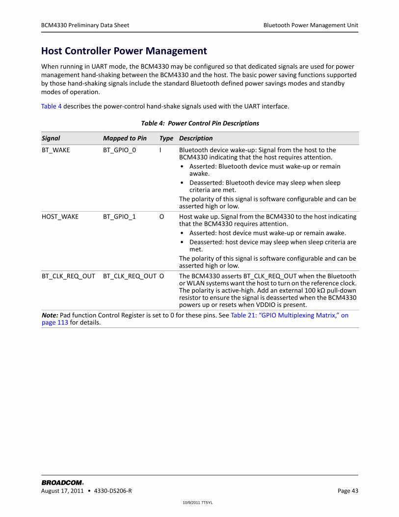
10/9/2011 7T5YL
Bluetooth Power Management Unit
BROADCOM August 17, 2011 • 4330-DS206-R Page 43
®
BCM4330 Preliminary Data Sheet
Host Controller Power ManagementWhen running in UART mode, the BCM4330 may be configured so that dedicated signals are used for power management hand-shaking between the BCM4330 and the host. The basic power saving functions supported by those hand-shaking signals include the standard Bluetooth defined power savings modes and standby modes of operation.
Table 4 describes the power-control hand-shake signals used with the UART interface.
Table 4: Power Control Pin Descriptions
Signal Mapped to Pin Type Description
BT_WAKE BT_GPIO_0 I Bluetooth device wake-up: Signal from the host to the BCM4330 indicating that the host requires attention.• Asserted: Bluetooth device must wake-up or remain
awake.• Deasserted: Bluetooth device may sleep when sleep
criteria are met.The polarity of this signal is software configurable and can be asserted high or low.
HOST_WAKE BT_GPIO_1 O Host wake up. Signal from the BCM4330 to the host indicating that the BCM4330 requires attention.• Asserted: host device must wake-up or remain awake.• Deasserted: host device may sleep when sleep criteria are
met.The polarity of this signal is software configurable and can be asserted high or low.
BT_CLK_REQ_OUT BT_CLK_REQ_OUT O The BCM4330 asserts BT_CLK_REQ_OUT when the Bluetooth or WLAN systems want the host to turn on the reference clock. The polarity is active-high. Add an external 100 kΩ pull-down resistor to ensure the signal is deasserted when the BCM4330 powers up or resets when VDDIO is present.
Note: Pad function Control Register is set to 0 for these pins. See Table 21: “GPIO Multiplexing Matrix,” on page 113 for details.

10/9/2011 7T5YL
Bluetooth Power Management Unit
BROADCOM August 17, 2011 • 4330-DS206-R Page 44
®
BCM4330 Preliminary Data Sheet
Figure 8: Startup Signaling Sequence
Note: Successful operation of the power management hand-shaking signals requires coordination between the BCM4330 firmware and the host software (see Figure 8).
HostResetX
VDDIO
LPO
BT_UART_RTS_N
CLK_REQ_OUT
BT_REG_ON
BT_UART_CTS_N
Host IOs configured
Host IOs unconfigured
BTH IOs configuredBTH IOs unconfigured
T3
Tsettle
T4
T1
Notes : T1 is the time for host to settle its IOs after a reset. T2 is the time for the BTH device to settle its IOs after a reset and ref clk settling time elapsed. T3 is the time for the BT device to complete initialization and drive BT_UART_RTS_N low. T4 is the setup time for BT_WAKE prior to driving BT_REG_ON high; BT_WAKEUP must be high
prior to BT_REG_ON being released. BT_WAKEUP should not be driven low until after configuration has been completed by the host.
Tsettle is the time for the ref clk signal from the host to be guaranteed to have settled.
Driven
Pulled
Indicates that BTH device is ready.

10/9/2011 7T5YL
Bluetooth Power Management Unit
BROADCOM August 17, 2011 • 4330-DS206-R Page 45
®
BCM4330 Preliminary Data Sheet
BBC Power ManagementThe following are low-power operations for the BBC:
• Physical layer packet-handling turns the RF on and off dynamically within transmit/receive packets.
• Bluetooth-specified low-power connection modes: sniff, hold, and park. While in these modes, the BCM4330 runs on the low-power oscillator and wakes up after a predefined time period.
• A low-power shutdown feature allows the device to be turned off while the host and any other devices in the system remain operational. When the BCM4330 is not needed in the system, the RF and core supplies are shut down while the I/O remains powered. This allows the BCM4330 to effectively be off while keeping the I/O pins powered so they do not draw extra current from any other devices connected to the I/O.
During the low-power shut-down state, provided VDDIO remains applied to the BCM4330, all outputs are tri-stated, and most input signals are disabled. Input voltages must remain within the limits defined for normal operation. This is done to prevent current paths or create loading on any digital signals in the system and enables the BCM4330 to be fully integrated in an embedded device to take full advantage of the lowest power-saving modes.
Two BCM4330 input signals are designed to be high-impedance inputs that do not load the driving signal even if the chip does not have VDDIO power supplied to it: the frequency reference input (WRF_TCXO_IN) and the 32.768 kHz input (LPO). When the BCM4330 is powered on from this state, it is the same as a normal power-up, and the device does not contain any information about its state from the time before it was powered down.
FM Power ManagementThe BCM4330 FM subsystem can operate independently of, or in tandem with, the Bluetooth RF and BBC subsystems. The FM subsystem power management scheme operates in conjunction with the Bluetooth RF and BBC subsystems. The FM block does not have a low power state, it is either on or off.
Low-Power ScanThe BCM4330 has an optional low-power scan mode that replaces conventional page/inquiry scans with a proprietary scan scheme. When this mode is activated, it significantly reduces current consumption for page and inquiry scans. The mode will switch to conventional scans if energy in page/inquiry channels with an appropriate activation pattern is detected.
Wideband SpeechThe BCM4330 provides support for wideband speech (WBS) using on-chip Smart Audio technology. The BCM4330 can perform subband-codec (SBC), as well as mSBC, encoding and decoding of linear 16 bits at 16 kHz (256 kbps rate) transferred over the PCM bus.

10/9/2011 7T5YL
Bluetooth Power Management Unit
BROADCOM August 17, 2011 • 4330-DS206-R Page 46
®
BCM4330 Preliminary Data Sheet
Packet Loss ConcealmentPacket Loss Concealment (PLC) improves apparent audio quality for systems with marginal link performance. Bluetooth messages are sent in packets. When a packet is lost, it creates a gap in the received audio bit-stream. Packet loss can be mitigated in several ways:
• Fill in zeros.
• Ramp down the output audio signal toward zero (this is the method used in current Bluetooth headsets).
• Repeat the last frame (or packet) of the received bit-stream and decode it as usual (frame repeat).
These techniques cause distortion and popping in the audio stream. The BCM4330 uses a proprietary waveform extension algorithm to provide dramatic improvement in the audio quality. Figure 9 and Figure 10 show audio waveforms with and without Packet Loss Concealment. Broadcom PLC/BEC algorithms also support wide band speech.
Figure 9: CVSD Decoder Output Waveform Without PLC
Figure 10: CVSD Decoder Output Waveform After Applying PLC
Audio Rate-Matching AlgorithmsThe BCM4330 has an enhanced rate-matching algorithm that uses interpolation algorithms to reduce audio stream jitter that may be present when the rate of audio data coming from the host is not the same as the Bluetooth or FM audio data rates.
Packet Loss Causes Ramp-Down

10/9/2011 7T5YL
Adaptive Frequency Hopping
BROADCOM August 17, 2011 • 4330-DS206-R Page 47
®
BCM4330 Preliminary Data Sheet
Codec EncodingThe BCM4330 can support SBC and mSBC encoding and decoding for wideband speech.
Multiple Simultaneous A2DP Audio StreamThe BCM4330 has the ability to take a single audio stream and output it to multiple Bluetooth devices simultaneously. This allows a user to share his or her music (or any audio stream) with a friend.
FM Over BluetoothFM Over Bluetooth enables the BCM4330 to stream data from FM over Bluetooth without requiring the host to be awake. This can significantly extend battery life for usage cases where someone is listening to FM radio on a Bluetooth headset.
Burst Buffer OperationThe BCM4330 has a data buffer that can buffer data being sent over the HCI and audio transports, then send the data at an increased rate. This mode of operation allows the host to sleep for the maximum amount of time, dramatically reducing system current consumption.
Adaptive Frequency HoppingThe BCM4330 gathers link quality statistics on a channel by channel basis to facilitate channel assessment and channel map selection. The link quality is determined using both RF and baseband signal processing to provide a more accurate frequency-hop map.
10/9/2011 7T5YL
Advanced Bluetooth/WLAN Coexistence
BROADCOM August 17, 2011 • 4330-DS206-R Page 48
®
BCM4330 Preliminary Data Sheet
Advanced Bluetooth/WLAN CoexistenceThe BCM4330 includes advanced coexistence technologies that are only possible with a Bluetooth/WLAN integrated die solution. These coexistence technologies are targeted at small form-factor platforms, such as cell phones and media players, including applications such as VoWLAN + SCO and Video-over-WLAN + High Fidelity BT Stereo.
Support is provided for platforms that share a single antenna between Bluetooth and 802.11g. Dual-antenna applications are also supported. The BCM4330 radio architecture allows for lossless simultaneous Bluetooth and WLAN reception for shared antenna applications. This is possible only via an integrated solution (shared LNA and joint AGC algorithm). It has superior performance versus implementations that need to arbitrate between Bluetooth and WLAN reception.
The BCM4330 integrated solution enables MAC-layer signaling (firmware) and a greater degree of sharing via an enhanced coexistence interface. Information is exchanged between the Bluetooth and WLAN cores without host processor involvement.
The BCM4330 also supports Transmit Power Control on the STA together with standard Bluetooth TPC to limit mutual interference and receiver desensitization. Preemption mechanisms are utilized to prevent AP transmissions from colliding with Bluetooth frames. Improved channel classification techniques have been implemented in Bluetooth for faster and more accurate detection and elimination of interferers (including non-WLAN 2.4 GHz interference).
The Bluetooth AFH classification is also enhanced by the WLAN core’s channel information.
Fast Connection (Interlaced Page and Inquiry Scans)The BCM4330 supports page scan and inquiry scan modes that significantly reduce the average inquiry response and connection times. These scanning modes are compatible with the Bluetooth version 2.1 page and inquiry procedures.
10/9/2011 7T5YL
Music and Audio
BROADCOM August 17, 2011 • 4330-DS206-R Page 49
®
BCM4330 Preliminary Data Sheet
Section 6: Music and Audio
The BCM4330 provides superior total system current during music or audio playback and recording. To enable these functions, several features of the device are combined to provide superior system power consumption.
MP3 Encoder• ISO/IEC 11172-3 compliant
• Supports 32 kHz sampling frequencies only
• Encodes mono and stereo signals
MP3 DecoderThe MP3 decoder supports mono and stereo audio recording with the following specifications:
• Supports MPEG-1 Layer 3 decoding
• Output is fully bit compliant with MPEG-1 standard specification
• Supports sampling frequencies from 32 kHz to 48 kHz
• Minimum bit-rate supported 32 Kbps and maximum bit-rate supported 320 Kbps for Layer 3
AAC/AAC+ DecoderCompliant to ISO/IEC 14496-3: 2004 specifications:
• MPEG-2, MPEG-4 AAC LC decoding up to level 2
• SBR tool, up to level 3
• Low power SBR tool
• Full support up to level 3 for the HE AAC profile
• Implicit and explicit SBR signaling mechanisms
• Mono and stereo channel streams decoding sampling frequencies from 8 kHz to 96 kHz only
• ADTS frame decoding
10/9/2011 7T5YL
Microprocessor and Memory Unit for Bluetooth
BROADCOM August 17, 2011 • 4330-DS206-R Page 50
®
BCM4330 Preliminary Data Sheet
Section 7: Microprocessor and Memory Unit for Bluetooth
The Bluetooth microprocessor core is based on the ARM® Cortex™-M3 32-bit RISC processor with embedded ICE-RT debug and JTAG interface units. It runs software from the link control (LC) layer, up to the host controller interface (HCI).
The ARM core is paired with a memory unit that contains 560 KB of ROM memory for program storage and boot ROM, 152 KB of RAM for data scratchpad and patch RAM code. The internal ROM allows for flexibility during power-on reset to enable the same device to be used in various configurations. At power-up, the lower-layer protocol stack is executed from the internal ROM memory.
External patches may be applied to the ROM-based firmware to provide flexibility for bug fixes or features additions. These patches may be downloaded from the host to the BCM4330 through the UART transports. The mechanism for downloading via UART is identical to the proven interface of the BCM4329 device.
RAM, ROM, and Patch MemoryThe BCM4330 Bluetooth core has 152 KB of internal RAM which is mapped between general purpose scratch pad memory and patch memory and 560 KB of ROM used for the lower-layer protocol stack, test mode software, and boot ROM. The patch memory capability enables the addition of code changes for purposes of feature additions and bug fixes to the ROM memory.
ResetThe BCM4330 has an integrated power-on reset circuit that resets all circuits to a known power-on state. The reset can also be driven by an active-low, external reset signal, BT_RST_N, that can be used to externally control the device, forcing it into a power-on reset state. (Note that the BT_RST_N signal is independent of the POR reset.)
10/9/2011 7T5YL
Bluetooth Peripheral Transport Unit
BROADCOM August 17, 2011 • 4330-DS206-R Page 51
®
BCM4330 Preliminary Data Sheet
Section 8: Bluetooth Peripheral Transport Unit
PCM InterfaceThe BCM4330 supports two independent PCM interfaces that share the pins with the I2S interfaces. The PCM Interface on the BCM4330 can connect to linear PCM Codec devices in master or slave mode. In master mode, the BCM4330 generates the PCM_CLK and PCM_SYNC signals, and in slave mode, these signals are provided by another master on the PCM interface and are inputs to the BCM4330.
The configuration of the PCM interface may be adjusted by the host through the use of vendor-specific HCI commands.
Slot MappingThe BCM4330 supports up to three simultaneous full-duplex SCO or eSCO channels through the PCM interface. These three channels are time-multiplexed onto the single PCM interface by using a time-slotting scheme where the 8 kHz or 16 kHz audio sample interval is divided into as many as 16 slots. The number of slots is dependent on the selected interface rate of 128 kHz, 512 kHz, or 1024 kHz. The corresponding number of slots for these interface rate is 1, 2, 4, 8, and 16, respectively. Transmit and receive PCM data from an SCO channel is always mapped to the same slot. The PCM data output driver tri-states its output on unused slots to allow other devices to share the same PCM interface signals. The data output driver tri-states its output after the falling edge of the PCM clock during the last bit of the slot.
Frame SynchronizationThe BCM4330 supports both short- and long-frame synchronization in both master and slave modes. In short-frame synchronization mode, the frame synchronization signal is an active-high pulse at the audio frame rate that is a single-bit period in width and is synchronized to the rising edge of the bit clock. The PCM slave looks for a high on the falling edge of the bit clock and expects the first bit of the first slot to start at the next rising edge of the clock. In long-frame synchronization mode, the frame synchronization signal is again an active-high pulse at the audio frame rate; however, the duration is three bit periods and the pulse starts coincident with the first bit of the first slot.
Data FormattingThe BCM4330 may be configured to generate and accept several different data formats. For conventional narrowband speech mode, the BCM4330 uses 13 of the 16 bits in each PCM frame. The location and order of these 13 bits can be configured to support various data formats on the PCM interface. The remaining three bits are ignored on the input and may be filled with 0s, 1s, a sign bit, or a programmed value on the output. The default format is 13-bit 2’s complement data, left justified, and clocked MSB first.

10/9/2011 7T5YL
PCM Interface
BROADCOM August 17, 2011 • 4330-DS206-R Page 52
®
BCM4330 Preliminary Data Sheet
Wideband Speech SupportWhen the host encodes Wideband Speech (WBS) packets in transparent mode, the encoded packets are transferred over the PCM bus for an eSCO voice connection. In this mode, the PCM bus is typically configured in master mode for a 4 kHz sync rate with 16-bit samples, resulting in a 64 kbps bit rate. The BCM4330 also supports slave transparent mode using a proprietary rate-matching scheme. In SBC-code mode, linear 16-bit data at 16 kHz (256 kbps rate) is transferred over the PCM bus.
Multiplexed Bluetooth and FM Over PCMIn this mode of operation, the BCM4330 multiplexes both FM and Bluetooth audio PCM channels over the same interface, reducing the number of required I/Os. This mode of operation is initiated through an HCI command from the host. The format of the data stream consists of three channels: a Bluetooth channel followed by two FM channels (audio left and right). In this mode of operation, the bus data rate only supports 48 kHz operation per channel with 16 bits sent for each channel. This is done to allow the low data rate Bluetooth data to coexist in the same interface as the higher speed I2S data. To accomplish this, the Bluetooth data is repeated six times for 8 kHz data and three times for 16 kHz data. An initial sync pulse on the PCM_SYNC line is used to indicate the beginning of the frame.
To support multiple Bluetooth audio streams within the Bluetooth channel, both 16 kHz and 8 kHz streams can be multiplexed. This mode of operation is only supported when the Bluetooth host is the master. Figure 11 shows the operation of the multiplexed transport with three simultaneous SCO connections. To accommodate additional SCO channels, the transport clock speed is increased. To change between modes of operation, the transport must be halted and restarted in the new configuration.
Figure 11: Functional Multiplex Data Diagram
Burst PCM ModeIn this mode of operation, the PCM bus runs at a significantly higher rate of operation to allow the host to duty cycle its operation and save current. In this mode of operation, the PCM bus can operate at a rate of up to 24 MHz. This mode of operation is initiated with an HCI command from the host.
PCM_SYNC
PCM_IN
PCM_OUT
FM right FM left
FM right FM left
BT SCO 1 TX BT SCO 2 TX BT SCO 3 TX
BT SCO 1 RX BT SCO 2 RX BT SCO 3 RX
1 frame
PCM_CLK
16 bits per SCO frame
CLK
16 bits per frame 16 bits per frame
Each SCO channel duplicates the data 6 times. Each WBS frame duplicates the data 3 times per frame

10/9/2011 7T5YL
PCM Interface
BROADCOM August 17, 2011 • 4330-DS206-R Page 53
®
BCM4330 Preliminary Data Sheet
PCM Interface Timing
Short Frame Sync, Master Mode
Figure 12: PCM Timing Diagram (Short Frame Sync, Master Mode)
Table 5: PCM Interface Timing Specifications (Short Frame Sync, Master Mode)
Ref No. Characteristics Minimum Typical Maximum Unit
1 PCM bit clock frequency – – 12 MHz
2 PCM bit clock HIGH 41 – – ns
3 PCM bit clock LOW 41 – – ns
4 PCM_SYNC delay 0 – 25 ns
5 PCM_OUT delay 0 – 25 ns
6 PCM_IN setup 8 – – ns
7 PCM_IN hold 8 – – ns
8 Delay from rising edge of PCM_BCLK during last bit period to PCM_OUT becoming high impedance
0 – 25 ns
PCM_BCLK
PCM_SYNC
PCM_OUT
12 3
4
5
PCM_IN
6
8
HIGH IMPEDANCE
7

10/9/2011 7T5YL
PCM Interface
BROADCOM August 17, 2011 • 4330-DS206-R Page 54
®
BCM4330 Preliminary Data Sheet
Short Frame Sync, Slave Mode
Figure 13: PCM Timing Diagram (Short Frame Sync, Slave Mode)
Table 6: PCM Interface Timing Specifications (Short Frame Sync, Slave Mode)
Ref No. Characteristics Minimum Typical Maximum Unit
1 PCM bit clock frequency – – 12 MHz
2 PCM bit clock HIGH 41 – – ns
3 PCM bit clock LOW 41 – – ns
4 PCM_SYNC setup 8 – – ns
5 PCM_SYNC hold 8 – – ns
6 PCM_OUT delay 0 – 25 ns
7 PCM_IN setup 8 – – ns
8 PCM_IN hold 8 – – ns
9 Delay from rising edge of PCM_BCLK during last bit period to PCM_OUT becoming high impedance
0 – 25 ns
PCM_BCLK
PCM_SYNC
PCM_OUT
12 3
4
5
6
PCM_IN
7
9
HIGH IMPEDANCE
8

10/9/2011 7T5YL
PCM Interface
BROADCOM August 17, 2011 • 4330-DS206-R Page 55
®
BCM4330 Preliminary Data Sheet
Long Frame Sync, Master Mode
Figure 14: PCM Timing Diagram (Long Frame Sync, Master Mode)
Table 7: PCM Interface Timing Specifications (Long Frame Sync, Master Mode)
Ref No. Characteristics Minimum Typical Maximum Unit
1 PCM bit clock frequency – – 12 MHz
2 PCM bit clock HIGH 41 – – ns
3 PCM bit clock LOW 41 – – ns
4 PCM_SYNC delay 0 – 25 ns
5 PCM_OUT delay 0 – 25 ns
6 PCM_IN setup 8 – – ns
7 PCM_IN hold 8 – – ns
8 Delay from rising edge of PCM_BCLK during last bit period to PCM_OUT becoming high impedance
0 – 25 ns
PCM_BCLK
PCM_SYNC
PCM_OUT
12 3
4
5
PCM_IN
6
8
HIGH IMPEDANCE
7
Bit 0
Bit 0
Bit 1
Bit 1

10/9/2011 7T5YL
PCM Interface
BROADCOM August 17, 2011 • 4330-DS206-R Page 56
®
BCM4330 Preliminary Data Sheet
Long Frame Sync, Slave Mode
Figure 15: PCM Timing Diagram (Long Frame Sync, Slave Mode)
Table 8: PCM Interface Timing Specifications (Long Frame Sync, Slave Mode)
Ref No. Characteristics Minimum Typical Maximum Unit
1 PCM bit clock frequency – – 12 MHz
2 PCM bit clock HIGH 41 – – ns
3 PCM bit clock LOW 41 – – ns
4 PCM_SYNC setup 8 – – ns
5 PCM_SYNC hold 8 – – ns
6 PCM_OUT delay 0 – 25 ns
7 PCM_IN setup 8 – – ns
8 PCM_IN hold 8 – – ns
9 Delay from rising edge of PCM_BCLK during last bit period to PCM_OUT becoming high impedance
0 – 25 ns
PCM_BCLK
PCM_SYNC
PCM_OUT
12 3
4
5
6
PCM_IN
7
9
HIGH IMPEDANCE
8
Bit 0
Bit 0
Bit 1
Bit 1

10/9/2011 7T5YL
PCM Interface
BROADCOM August 17, 2011 • 4330-DS206-R Page 57
®
BCM4330 Preliminary Data Sheet
Short Frame Sync, Burst Mode
Figure 16: PCM Burst Mode Timing (Receive Only, Short Frame Sync)
Table 9: PCM Burst Mode (Receive Only, Short Frame Sync)
Ref No. Characteristics Minimum Typical Maximum Unit
1 PCM bit clock frequency – – 24 MHz
2 PCM bit clock HIGH 20.8 – – ns
3 PCM bit clock LOW 20.8 – – ns
4 PCM_SYNC setup 8 – – ns
5 PCM_SYNC hold 8 – – ns
6 PCM_IN setup 8 – – ns
7 PCM_IN hold 8 – – ns
PCM_BCLK
PCM_SYNC
12 3
45
PCM_IN
6 7

10/9/2011 7T5YL
PCM Interface
BROADCOM August 17, 2011 • 4330-DS206-R Page 58
®
BCM4330 Preliminary Data Sheet
Long Frame Sync, Burst Mode
Figure 17: PCM Burst Mode Timing (Receive Only, Long Frame Sync)
Table 10: PCM Burst Mode (Receive Only, Long Frame Sync)
Ref No. Characteristics Minimum Typical Maximum Unit
1 PCM bit clock frequency – – 24 MHz
2 PCM bit clock HIGH 20.8 – – ns
3 PCM bit clock LOW 20.8 – – ns
4 PCM_SYNC setup 8 – – ns
5 PCM_SYNC hold 8 – – ns
6 PCM_IN setup 8 – – ns
7 PCM_IN hold 8 – – ns
PCM_BCLK
PCM_SYNC
12 3
45
PCM_IN
6 7
Bit 0 Bit 1

10/9/2011 7T5YL
UART Interface
BROADCOM August 17, 2011 • 4330-DS206-R Page 59
®
BCM4330 Preliminary Data Sheet
UART InterfaceThe BCM4330 shares a single UART for Bluetooth and FM. The UART is a standard 4-wire interface (RX, TX, RTS, and CTS) with adjustable baud rates from 9600 bps to 4.0 Mbps. The interface features an automatic baud rate detection capability that returns a baud rate selection. Alternatively, the baud rate may be selected through a vendor-specific UART HCI command.
UART has a 1040-byte receive FIFO and a 1040-byte transmit FIFO to support EDR. Access to the FIFOs is conducted through the AHB interface through either DMA or the CPU. The UART supports the Bluetooth 4.0 UART HCI specification: H4, a custom Extended H4, and H5. The default baud rate is 115.2 Kbaud.
The UART supports the 3-wire H5 UART transport, as described in the Bluetooth specification (“Three-wire UART Transport Layer”). Compared to H4, the H5 UART transport reduces the number of signal lines required by eliminating the CTS and RTS signals.
The BCM4330 UART can perform XON/XOFF flow control and includes hardware support for the Serial Line Input Protocol (SLIP). It can also perform wake-on activity. For example, activity on the RX or CTS inputs can wake the chip from a sleep state.
Normally, the UART baud rate is set by a configuration record downloaded after device reset, or by automatic baud rate detection, and the host does not need to adjust the baud rate. Support for changing the baud rate during normal HCI UART operation is included through a vendor-specific command that allows the host to adjust the contents of the baud rate registers. The BCM4330 UARTs operate correctly with the host UART as long as the combined baud rate error of the two devices is within ±2%.
Table 11: Example of Common Baud Rates
Desired Rate Actual Rate Error (%)
4000000 4000000 0.00
3692000 3692308 0.01
3000000 3000000 0.00
2000000 2000000 0.00
1500000 1500000 0.00
1444444 1454544 0.70
921600 923077 0.16
460800 461538 0.16
230400 230796 0.17
115200 115385 0.16
57600 57692 0.16
38400 38400 0.00
28800 28846 0.16
19200 19200 0.00
14400 14423 0.16
9600 9600 0.00

10/9/2011 7T5YL
UART Interface
BROADCOM August 17, 2011 • 4330-DS206-R Page 60
®
BCM4330 Preliminary Data Sheet
Figure 18: UART Timing
Table 12: UART Timing Specifications
Ref No. Characteristics Minimum Typical Maximum Unit
1 Delay time, UART_CTS_N low to UART_TXD valid – – 1.5 Bit periods
2 Setup time, UART_CTS_N high before midpoint of stop bit
– – 0.5 Bit periods
3 Delay time, midpoint of stop bit to UART_RTS_N high
– – 0.5 Bit periods
UART_CTS_N
UART_RXD
UART_RTS_N
1 2
Midpoint of STOP bit
UART_TXD
Midpoint of STOP bit
3

10/9/2011 7T5YL
I2S Interface
BROADCOM August 17, 2011 • 4330-DS206-R Page 61
®
BCM4330 Preliminary Data Sheet
I2S InterfaceThe BCM4330 supports two independent I2S digital audio ports: one for Bluetooth audio, and one for high-fidelity FM audio. The I2S interface for FM audio supports both master and slave modes. The I2S signals are:
• I2S clock: I2S SCK
• I2S Word Select: I2S WS
• I2S Data Out: I2S SDO
• I2S Data In: I2S SDI
I2S SCK and I2S WS become outputs in master mode and inputs in slave mode, while I2S SDO always stays as an output. I2S data input is used for FM Tx. The channel word length is 16 bits and the data is justified so that the MSB of the left-channel data is aligned with the MSB of the I2S bus, per the I2S specification. The MSB of each data word is transmitted one bit clock cycle after the I2S WS transition, synchronous with the falling edge of bit clock. Left-channel data is transmitted when I2S WS is low, and right-channel data is transmitted when I2S WS is high. Data bits sent by the BCM4330 are synchronized with the falling edge of I2S_SCK and should be sampled by the receiver on the rising edge of I2S_SSCK.
The clock rate in master mode is either of the following:
48 kHz x 32 bits per frame = 1.536 MHz
48 kHz x 50 bits per frame = 2.400 MHz
The master clock is generated from the input reference clock using a N/M clock divider.
In the slave mode, any clock rate is supported to a maximum of 3.072 MHz.
I2S Timing
Note: Timing values specified in Table 13 are relative to high and low threshold levels.
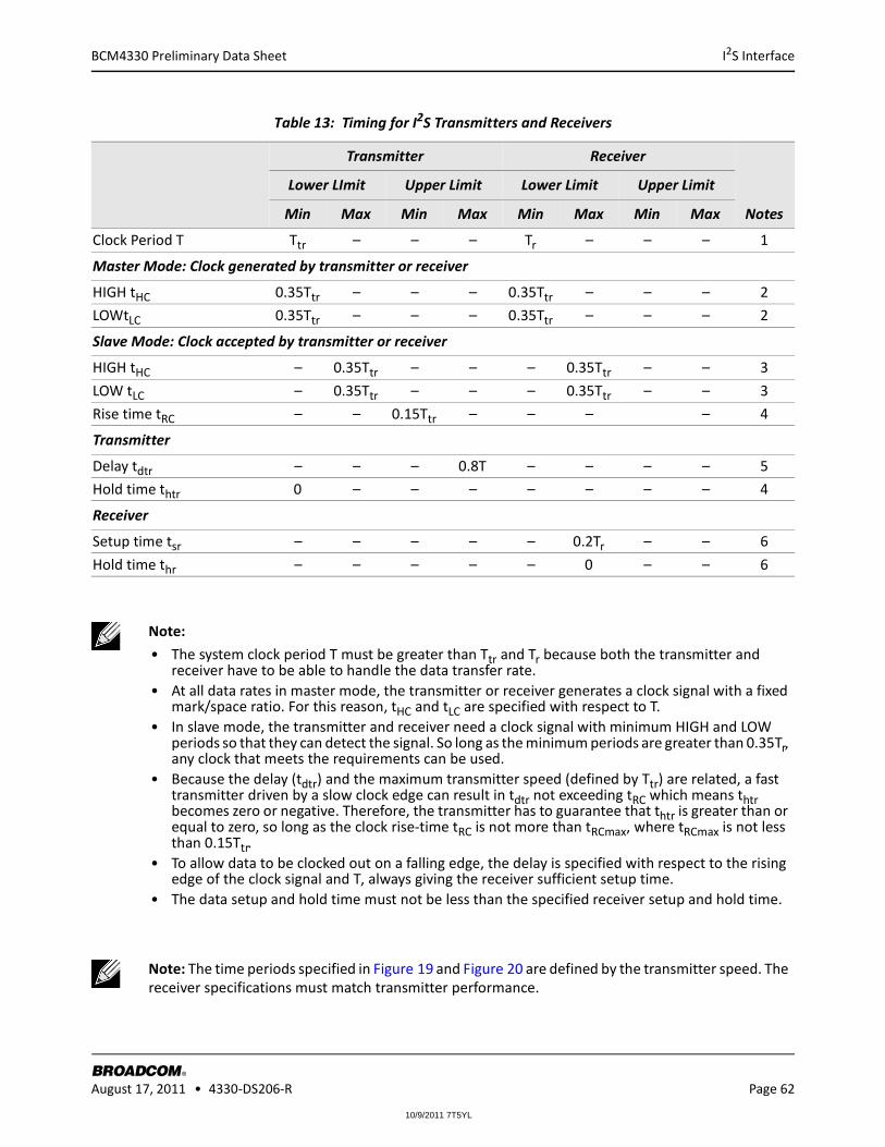
10/9/2011 7T5YL
I2S Interface
BROADCOM August 17, 2011 • 4330-DS206-R Page 62
®
BCM4330 Preliminary Data Sheet
Table 13: Timing for I2S Transmitters and Receivers
Transmitter Receiver
Notes
Lower LImit Upper Limit Lower Limit Upper Limit
Min Max Min Max Min Max Min Max
Clock Period T Ttr – – – Tr – – – 1
Master Mode: Clock generated by transmitter or receiver
HIGH tHC 0.35Ttr – – – 0.35Ttr – – – 2
LOWtLC 0.35Ttr – – – 0.35Ttr – – – 2
Slave Mode: Clock accepted by transmitter or receiver
HIGH tHC – 0.35Ttr – – – 0.35Ttr – – 3
LOW tLC – 0.35Ttr – – – 0.35Ttr – – 3
Rise time tRC – – 0.15Ttr – – – – 4
Transmitter
Delay tdtr – – – 0.8T – – – – 5
Hold time thtr 0 – – – – – – – 4
Receiver
Setup time tsr – – – – – 0.2Tr – – 6
Hold time thr – – – – – 0 – – 6
Note:
• The system clock period T must be greater than Ttr and Tr because both the transmitter and receiver have to be able to handle the data transfer rate.
• At all data rates in master mode, the transmitter or receiver generates a clock signal with a fixed mark/space ratio. For this reason, tHC and tLC are specified with respect to T.
• In slave mode, the transmitter and receiver need a clock signal with minimum HIGH and LOW periods so that they can detect the signal. So long as the minimum periods are greater than 0.35Tr, any clock that meets the requirements can be used.
• Because the delay (tdtr) and the maximum transmitter speed (defined by Ttr) are related, a fast transmitter driven by a slow clock edge can result in tdtr not exceeding tRC which means thtr becomes zero or negative. Therefore, the transmitter has to guarantee that thtr is greater than or equal to zero, so long as the clock rise-time tRC is not more than tRCmax, where tRCmax is not less than 0.15Ttr.
• To allow data to be clocked out on a falling edge, the delay is specified with respect to the rising edge of the clock signal and T, always giving the receiver sufficient setup time.
• The data setup and hold time must not be less than the specified receiver setup and hold time.
Note: The time periods specified in Figure 19 and Figure 20 are defined by the transmitter speed. The receiver specifications must match transmitter performance.

10/9/2011 7T5YL
I2S Interface
BROADCOM August 17, 2011 • 4330-DS206-R Page 63
®
BCM4330 Preliminary Data Sheet
Figure 19: I2S Transmitter Timing
Figure 20: I2S Receiver Timing
SD and WS
SCKVL = 0.8V
tLC > 0.35TtRC*
tHC > 0.35T
T
VH = 2.0V
thtr > 0
totr < 0.8T
T = Clock periodTtr = Minimum allowed clock period for transmitterT = Ttr
* tRC is only relevant for transmitters in slave mode.
SD and WS
SCKVL = 0.8V
tLC > 0.35T tHC > 0.35
T
VH = 2.0V
thr > 0tsr > 0.2T
T = Clock periodTr = Minimum allowed clock period for transmitterT > Tr

10/9/2011 7T5YL
FM Transceiver Subsystem
BROADCOM August 17, 2011 • 4330-DS206-R Page 64
®
BCM4330 Preliminary Data Sheet
Section 9: FM Transceiver Subsystem
FM RadioThe BCM4330 includes a completely integrated FM radio receiver and transmitter with RDS/RBDS covering all FM bands from 65 MHz to 108 MHz. The transceiver is controlled through commands on the HCI. FM received audio is available as stereo analog output or in digital form through I2S or PCM. The FM audio to be transmitted can be delivered via the I2S or PCM interface. The FM radio is capable of operating from the 32.768 kHz LPO clock.
Digital FM Audio InterfacesThe FM audio can be received or transmitted via the shared PCM and I2S pins, and the sampling rate is nominally at 48 kHz. The BCM4330 supports a three-wire PCM or I2S audio interface in either master or slave configuration. The master or slave configuration is selected using vendor specific commands over the HCI interface. In addition, multiple sampling rates are supported, derived from either the FM or Bluetooth clocks. In master mode, the clock rate is either of the following:
• 48 kHz x 32 bits per frame = 1.536 MHz
• 48 kHz x 50 bits per frame = 2.400 MHz
In slave mode, any clock rate is supported up to a maximum of 3.072 MHz.
Analog FM Audio InterfacesThe demodulated FM audio signal is available as line-level analog stereo output, generated by twin internal high SNR audio DACs.
FM Over BluetoothThe BCM4330 can output received FM audio onto Bluetooth using one of following three links: eSCO, WBS, and A2DP. In all of the above modes, once the link has been set up, the host processor can enter sleep mode while the BCM4330 continues to stream FM audio to the remote Bluetooth device, allowing the system current consumption to be minimized.

10/9/2011 7T5YL
eSCO
BROADCOM August 17, 2011 • 4330-DS206-R Page 65
®
BCM4330 Preliminary Data Sheet
eSCOIn this use case, the stereo FM audio is downsampled to 8 kHz and a mono or stereo stream is then sent through the Bluetooth eSCO link to a remote Bluetooth device, typically a headset. Two Bluetooth voice connections must be used to transport stereo.
Wide Band Speech LinkIn this case, the stereo FM audio is downsampled to 16 kHz and a mono or stereo stream is then sent through the Bluetooth wideband speech link to a remote Bluetooth device, typically a headset. Two Bluetooth voice connections must be used to transport stereo.
A2DPIn this case, the stereo FM audio is encoded by the on-chip SBC encoder and transported as an A2DP link to a remote Bluetooth device. Sampling rates of 48 kHz, 44.1 kHz, and 32 kHz joint stereo are supported. An A2DP “lite” stack is implemented in the BCM4330 to support this use case, which eliminates the need to route the SBC-encoded audio back to the host to create the A2DP packets.
Dynamic Antenna SwitchingThe BCM4330 includes a circuit to detect the presence of ground-coupled antenna.

10/9/2011 7T5YL
Autotune and Search Algorithms
BROADCOM August 17, 2011 • 4330-DS206-R Page 66
®
BCM4330 Preliminary Data Sheet
Autotune and Search AlgorithmsThe BCM4330 supports a number of FM search and tune functions that allows the host to implement many convenient user functions, which are accessed through the Broadcom FM stack.
• Tune to Play — Allows the FM receiver to be programmed to a specific frequency.
• Search for RSSI > Threshold — Searches for valid FM channels within the band that have signal strength above a specified threshold. This function can be set to search for the next valid channel up or down the band or can be set to search for a list of valid channels across the entire band.
• Search for RSSI < Threshold — Searches for empty or under-utilized channels that can be used to transmit FM. Available channels can be identified before suggesting an FM transmit channel to the user. This allows the BCM4330 to determine the best channel for FM transmit operation instead of requiring the user to find an unused channel manually.
• Search for SNR > Threshold — Checks the power level of the available channel and the estimated SNR of the channel to help achieve precise control of the expected sound quality for the selected FM channel. Specifically, the host can adjust its SNR requirements to retrieve a signal with a specific sound quality, or adjust this to return the weakest channels.
• Alternate Frequency Jump — Allows the FM receiver to automatically jump to an alternate FM channel that carries the same information, but has a better SNR. For example, when traveling, a user may pass through a region where a number of channels carry the same station. When the user passes from one area to the next, the FM receiver can automatically switch to another channel with a stronger signal to spare the user from having to manually change the channel to continue listening to the same station.
Audio FeaturesA number of features are implemented in the BCM4330 to provide the best possible audio experience for the user.
• Mono/Stereo Blend or Switch — The BCM4330 provides automatic control of the stereo or mono settings based on the RSSI and estimated audio SNR. This feature is used to achieve a minimum audio SNR based on the channel conditions. Two modes of operation are supported:
– Blend — In this mode, fine control of stereo separation is used to achieve optimal audio quality over a wide range of input C/N. The amount of separation is fully programmable. In Figure 21, the separation is programmed to maintain a minimum 50 dB SNR across the blend range.
– Switch — In this mode, the audio switches from full stereo to full mono at a predetermined level to maintain optimal audio quality. The stereo-to-mono switch point and the mono-to-stereo switch points are fully programmable to provide the desired amount of audio SNR. In Figure 22, the switch point is programmed to switch to mono to maintain a 40 dB SNR.

10/9/2011 7T5YL
Audio Features
BROADCOM August 17, 2011 • 4330-DS206-R Page 67
®
BCM4330 Preliminary Data Sheet
Figure 21: Example Blend/Switch Usage
Figure 22: Example Blend/Switch Separation
• Soft Mute — Improves the user experience by dynamically muting the output audio proportionate to the FM signal C/N. This prevents the user from being assaulted with a blast of static. The mute characteristic is fully programmable to accommodate fine tuning of the output signal level. An example mute characteristic is shown in Figure 23.
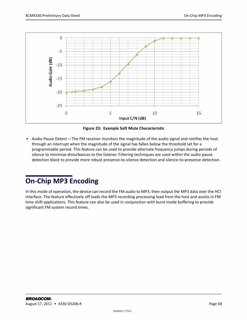
10/9/2011 7T5YL
On-Chip MP3 Encoding
BROADCOM August 17, 2011 • 4330-DS206-R Page 68
®
BCM4330 Preliminary Data Sheet
Figure 23: Example Soft Mute Characteristic
• Audio Pause Detect — The FM receiver monitors the magnitude of the audio signal and notifies the host through an interrupt when the magnitude of the signal has fallen below the threshold set for a programmable period. This feature can be used to provide alternate frequency jumps during periods of silence to minimize disturbances to the listener. Filtering techniques are used within the audio pause detection block to provide more robust presence-to-silence detection and silence-to-presence detection.
On-Chip MP3 EncodingIn this mode of operation, the device can record the FM audio to MP3, then output the MP3 data over the HCI interface. The feature effectively off loads the MP3 recording processing load from the host and assists in FM time shift applications. This feature can also be used in conjunction with burst mode buffering to provide significant FM system record times.

10/9/2011 7T5YL
RDS/RBDS
BROADCOM August 17, 2011 • 4330-DS206-R Page 69
®
BCM4330 Preliminary Data Sheet
RDS/RBDSThe BCM4330 integrates a RDS/RBDS modem and codec, the decoder includes programmable filtering and buffering functions, and the encoder includes the option to encode messages to PS or RT frame format with programmable scrolling in PS mode. The RDS/RBDS data can be read out in receive mode or delivered in transmit mode through the HCI interface.
In addition, the RDS/RBDS functionality supports the following:
Receive
• Block decoding, error correction and synchronization
• Flywheel synchronization feature, allowing the host to set parameters for acquisition, maintenance, and loss of sync. (It is possible to set up the BCM4330 such that synch is achieved when a minimum of two good blocks (error free) are decoded in sequence. The number of good blocks required for sync is programmable.)
• Storage capability up to 126 blocks of RDS data
• Full or partial block B match detect and interrupt to host
• Audio pause detection with programmable parameters
• Program Identification (PI) code detection and interrupt to host
• Automatic frequency jump
• Block E filtering
Transmit
• Support simple block encoding or RT/PS message to frame encoding (RT/PS mode minimizes host communication for improved system power saving)
• Programmable scroll rate in PS mode
• 256 bytes of storage for either RT/PS message or simple RDS/RBDS blocks
•
10/9/2011 7T5YL
WLAN Global Functions
BROADCOM August 17, 2011 • 4330-DS206-R Page 70
®
BCM4330 Preliminary Data Sheet
Section 10: WLAN Global Functions
WLAN CPU and Memory SubsystemThe BCM4330 includes an integrated ARM Cortex-M3™ processor with internal RAM and ROM. The ARM Cortex-M3 processor is a low-power processor that features low gate count, low interrupt latency, and low-cost debug. It is intended for deeply embedded applications that require fast interrupt response features. The processor implements the ARM architecture v7-M with support for Thumb®-2 instruction set. ARM Cortex-M3 delivers 30% more performance gain over ARM7TDMI.
At 0.19uW/MHz, the Cortex-M3 is the most power efficient general purpose microprocessor available, outperforming 8- and 16-bit devices on MIPS/uW. It supports integrated sleep modes.
ARM Cortex-M3 uses multiple technologies to reduce cost through improved memory utilization, reduced pin overhead, and reduced silicon area. ARM Cortex-M3 supports independent buses for Code and Data access (ICode/DCode and System buses). ARM Cortex-M3 supports extensive debug features including real time trace of program execution.
On-chip memory for the CPU includes 288 KB SRAM and 512 KB ROM.
One-Time-Programmable MemoryVarious hardware configuration parameters may be stored in an internal 2 Kbit one-time-programmable (OTP) memory, which is read by system software after device reset. In addition, customer-specific parameters, including the system vendor ID and the MAC address can be stored, depending on the specific board design.
The initial state of all bits in an unprogrammed OTP device is 0. After any bit is programmed to a 1, it cannot be reprogrammed to 0. The entire OTP array can be programmed in a single write cycle using a utility provided with the Broadcom WLAN manufacturing test tools. Alternatively, multiple write cycles can be used to selectively program specific bytes, but only bits which are still in the 0 state can be altered during each programming cycle.
Prior to OTP programming, all values should be verified using the appropriate editable nvram.txt file, which is provided with the reference board design package. Documentation on the OTP development process is available on the Broadcom customer support portal (http://www.broadcom.com/support).
10/9/2011 7T5YL
GPIO Interface
BROADCOM August 17, 2011 • 4330-DS206-R Page 71
®
BCM4330 Preliminary Data Sheet
GPIO InterfaceThere are seven general purpose I/O (GPIO) pins available on the WLAN section of the BCM4330 that can be used to connect to various external devices.
Upon power up and reset, these pins become tri-stated. Subsequently, they can be programmed to be either input or output pins via the GPIO control register. An internal pull-up resistor is included on each GPIO. If a GPIO output enable is not asserted, and the corresponding GPIO signal is not being driven externally, the GPIO is read as high.
External Coexistence InterfaceAn external handshake interface is available to enable signaling between the device and an external co-located wireless device, such as GPS, WiMax, or UWB, to manage wireless medium sharing for optimum performance. The following signals can be enabled by software on the indicated WL_GPIO pins:
• ERCX_STATUS — WL_GPIO1
• ERCX_FREQ — WL_GPIO2
• ERCX_RF_ACTIVE — WL_GPIO3
• ERCX_TXCONF — WL_GPIO4
• ERCX_PRISEL — WL_GPIO5
UART Interface One UART interface can be enabled by software as an alternate function on pins WL_GPIO4 and WL_GPIO_3. Provided primarily for debugging during development, this UART enables the BCM4330 to operate as RS-232 data termination equipment (DTE) for exchanging and managing data with other serial devices. It is compatible with the industry standard 16550 UART, and it provides a FIFO size of 64 × 8 in each direction.
JTAG InterfaceThe BCM4330 supports the IEEE 1149.1 JTAG boundary scan standard for performing device package and PCB assembly testing during manufacturing. In addition, the JTAG interface allows Broadcom to assist customers by using proprietary debug and characterization test tools during board bringup. Therefore, it is highly recommended to provide access to the JTAG pins by means of test points or a header on all PCB designs.
Caution! The BCM4330 I/O interface pins are not 3.3V tolerant. All I/O signaling should be limited to 2.9V ±3%, 2.5V, 1.8V, or 1.2V, depending on the I/O power supply voltage VDDIO. This applies to the GPIO, External Coexistence, UART, and JTAG signals.

10/9/2011 7T5YL
WLAN Host Interfaces
BROADCOM August 17, 2011 • 4330-DS206-R Page 72
®
BCM4330 Preliminary Data Sheet
Section 11: WLAN Host Interfaces
SDIO v2.0The BCM4330 WLAN section supports SDIO version 2.0. for both 1-bit (25 Mbps), 4-bit modes (100 Mbps), and high speed 4-bit (50 MHz clocks — 200 Mbps). It has the ability to map the interrupt signal onto a GPIO pin. This out-of-band interrupt signal notifies the host when the WLAN device wants to turn on the SDIO interface. The ability to force control of the gated clocks from within the WLAN chip is also provided.
SDIO mode is enabled using the strapping option pins strap_host_ifc_[3:1] (Table 19: “WLAN GPIO Functions and Strapping Options,” on page 112).
Three functions are supported:
• Function 0 Standard SDIO function (Max BlockSize/ByteCount = 32B)
• Function 1 Backplane Function to access the internal System On Chip (SOC) address space (Max BlockSize/ByteCount = 64B)
• Function 2 WLAN Function for efficient WLAN packet transfer through DMA (Max BlockSize/ByteCount = 512B)
SDIO Pin Descriptions
Caution! The SDIO interface pins are not 3.3V tolerant. All SDIO signaling should be limited to 2.9V ±3%, 2.5V, 1.8V, or 1.2V, depending on the I/O power supply voltage VDDIO.
Table 14: SDIO Pin Description
SD 4-Bit Mode SD 1-Bit Mode gSPI Mode
DATA0 Data line 0 DATA Data line DO Data output
DATA1 Data line 1 or Interrupt IRQ Interrupt IRQ Interrupt
DATA2 Data line 2 or Read Wait RW Read Wait NC Not used
DATA3 Data line 3 N/C Not used CS Card select
CLK Clock CLK Clock SCLK Clock
CMD Command line CMD Command line DI Data input

10/9/2011 7T5YL
SDIO v2.0
BROADCOM August 17, 2011 • 4330-DS206-R Page 73
®
BCM4330 Preliminary Data Sheet
Figure 24: Signal Connections to SDIO Host (SD 4-Bit Mode)
Figure 25: Signal Connections to SDIO Host (SD 1-Bit Mode)
SD Host BCM4330
CLK
CMD
DAT[3:0]
SD Host BCM4330
CLK
CMD
DATA
IRQ
RW
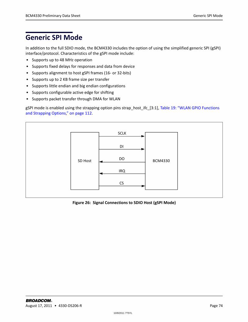
10/9/2011 7T5YL
Generic SPI Mode
BROADCOM August 17, 2011 • 4330-DS206-R Page 74
®
BCM4330 Preliminary Data Sheet
Generic SPI ModeIn addition to the full SDIO mode, the BCM4330 includes the option of using the simplified generic SPI (gSPI) interface/protocol. Characteristics of the gSPI mode include:
• Supports up to 48 MHz operation
• Supports fixed delays for responses and data from device
• Supports alignment to host gSPI frames (16- or 32-bits)
• Supports up to 2 KB frame size per transfer
• Supports little endian and big endian configurations
• Supports configurable active edge for shifting
• Supports packet transfer through DMA for WLAN
gSPI mode is enabled using the strapping option pins strap_host_ifc_[3:1], Table 19: “WLAN GPIO Functions and Strapping Options,” on page 112.
Figure 26: Signal Connections to SDIO Host (gSPI Mode)
SD Host BCM4330
SCLK
DI
DO
IRQ
CS

10/9/2011 7T5YL
Generic SPI Mode
BROADCOM August 17, 2011 • 4330-DS206-R Page 75
®
BCM4330 Preliminary Data Sheet
SPI ProtocolThe SPI protocol supports both 16-bit and 32-bit word operation. Byte endianess is supported in both modes. Figure 27 and Figure 28 show the basic write and write/read commands.
Figure 27: gSPI Write Protocol
Figure 28: gSPI Read Protocol
C1 C0 C3 C2 D1 D0 D3 D2 D5 D4 D7 D6
0000 0000 0000 0000 0000 0000
Din
Dout
C3 C2 C1 C0 D3 D2 D1 D0 D7 D6 D5 D4
0000 0000
Command
Dout 0000 0000 0000 0000
Data Data
Din
C0 C1 C2 C3 D0 D1 D2 D3 D4 D5 D6 D7
0000 0000Dout 0000 0000 0000 0000
Din32-bitBig endian
16-bitLittle endian
32-bitLittle endian
Write Protocol
C0 C1 C2 C3 D0 D1 D2 D3 D4 D5 D6 D7
0000 0000 0000 0000 0000 0000
Din
Dout
16-bitBig endian
C1 C0 C3 C2 xxxx xxxx xxxx xxxx
0000 0000 D1 D0 D3 D2 D5 D4 D7 D6
Din
Dout
C3 C2 C1 C0 xxxx xxxx xxxx xxxx
0000 0000
Command
Dout D3 D2 D1 D0 D7 D6 D5 D4
Data Data
Din
C0 C1 C2 C3 xxxx xxxx xxxx xxxx
0000 0000Dout D0 D1 D2 D3 D4 D5 D6 D7
Din32-bitBig endian
16-bitLittle endian
32-bitLittle endian
Read Protocol
C0 C1 C2 C3
D0 D1 D2 D3 D4 D5 D6 D70000 0000
Din
Dout
16-bitBig endian
Fixed Delay
Fixed Delay
Fixed Delay
Fixed Delay
xxxx xxxx xxxx xxxx
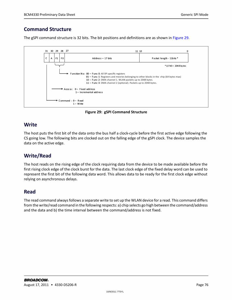
10/9/2011 7T5YL
Generic SPI Mode
BROADCOM August 17, 2011 • 4330-DS206-R Page 76
®
BCM4330 Preliminary Data Sheet
Command StructureThe gSPI command structure is 32 bits. The bit positions and definitions are as shown in Figure 29.
Figure 29: gSPI Command Structure
WriteThe host puts the first bit of the data onto the bus half a clock-cycle before the first active edge following the CS going low. The following bits are clocked out on the falling edge of the gSPI clock. The device samples the data on the active edge.
Write/ReadThe host reads on the rising edge of the clock requiring data from the device to be made available before the first rising clock edge of the clock burst for the data. The last clock edge of the fixed delay word can be used to represent the first bit of the following data word. This allows data to be ready for the first clock edge without relying on asynchronous delays.
ReadThe read command always follows a separate write to set up the WLAN device for a read. This command differs from the write/read command in the following respects: a) chip selects go high between the command/address and the data and b) the time interval between the command/address is not fixed.
01027 11
P acket length - 11b its *Ad dress – 17 bitsF1 F 0C A
F unction N o: 00 – F unc 001 – F unc 110 – F unc 211 – F unc 3
C ommand : 0 – R ead1 – Write
28293031
Acce ss : 0 – F ixed add ress1 – Incremental add res s
* 11’h0 = 204 8 by tes
01027 11
P acket length - 11b its *Ad dress – 17 bitsF1 F 0C A
F unction N o: 00 – F unc 01 – F unc 1: Registers and meories belonging to other blocks in the chip (64 bytes max)10 – F unc 2: DMA channel 1. WLAN packets up to 2048 bytes.11 – F unc !"#$%
C ommand : 0 – R ead1 – Write
28293031
Acce ss : 0 – F ixed add ress1 – Incremental add res s
* 11’h0 = 204 8 by tes

10/9/2011 7T5YL
Generic SPI Mode
BROADCOM August 17, 2011 • 4330-DS206-R Page 77
®
BCM4330 Preliminary Data Sheet
StatusThe gSPI interface supports status notification to the host after a read/write transaction. This status notification provides information about any packet errors, protocol errors, information about available packet in the RX queue, etc. The status information helps in reducing the number of interrupts to the host. The status-reporting feature can be switched off using a register bit, without any timing overhead. The gSPI bus timing for read/write transactions with and without status notification are as shown in Figure 30 and Figure 31 on page 78. See Table 15 on page 78 for information on status field details.
Figure 30: gSPI Signal Timing Without Status
C31 C30 C1 C0 D31 D30 D1 D0
Command 32 bits Write Data 16*n bits
cs
sclk
mosi
C31 C30 C0
D31 D30 D0
Command32 bits
Read Data16*n bits
miso
cs
sclk
mosi
ResponseDelay
C31 C30 C0
D31 D30 D0
Command32 bits
Read Data 16*n bits
miso
cs
sclk
mosi
ResponseDelay
D1
C31 C30 C1 C0 D31 D30 D1 D0
Command 32 bits Write Data 16*n bits
cs
sclk
mosi C31 C30 C1 C0 D31 D30 D1 D0C31 C30 C1 C0 D31 D30 D1 D0
Command 32 bits Write Data 16*n bits
cs
sclk
mosi
C31 C30 C0
D31 D30 D0
Command32 bits
Read Data16*n bits
miso
cs
sclk
mosi
ResponseDelay
C31 C30 C0
D31 D30 D0
Command32 bits
Read Data16*n bits
miso
cs
sclk
mosi
ResponseDelay
C31 C30 C0
D31 D30 D0
Command32 bits
Read Data 16*n bits
miso
cs
sclk
mosi
ResponseDelay
D1
C31 C30 C0
D31 D30 D0
Command32 bits
Read Data 16*n bits
miso
cs
sclk
mosi
ResponseDelay
D1
Write
Write-Read
Read

10/9/2011 7T5YL
Generic SPI Mode
BROADCOM August 17, 2011 • 4330-DS206-R Page 78
®
BCM4330 Preliminary Data Sheet
Figure 31: gSPI Signal Timing with Status (Response Delay = 0)
Table 15: gSPI Status Field Details
Bit Name Description
0 Data not available The requested read data is not available
1 Underflow FIFO underflow occurred due to current (F2, F3) read command
2 Overflow FIFO overflow occurred due to current (F1, F2, F3) write command
3 F2 interrupt F2 channel interrupt
4 F3 interrupt F3 channel interrupt
5 F2 RX Ready F2 FIFO is ready to receive data (FIFO empty)
6 F3 RX Ready F3 FIFO is ready to receive data (FIFO empty)
7 Reserved –
8 F2 Packet Available Packet is available/ready in F2 TX FIFO
9:19 F2 Packet Length Length of packet available in F2 FIFO
20 F3 Packet Available Packet is available/ready in F3 TX FIFO
21:31 F3 Packet Length Length of packet available in F3 FIFO
C31 C0
D31 D1 D0
Read Data 16*n bits
miso
cs
sclk
mosi
S0S31
Status 32 bits
C31 C0
D31 D1 D0
Command 32 bits Read Data 16*n bits
miso
cs
sclk
mosi
S0S31
Status 32 bits
C31
S0
C1 C0 D31
S31
D1 D0
Command 32 bits Write Data 16*n bits
cs
sclk
mosi
S1
Status 32 bits
miso
C31 C0
D31 D1 D0 S0S31
C31 C0
D31 D1 D0 S0S31
C31 C0
D31 D1 D0 S0S31
C31 C0
D31 D1 D0 S0S31
C31
S0
C1 C0 D31
S31
D1 D0
S1
C31
S0
C1 C0 D31
S31
D1 D0
S1
Command 32 bits
Write
Write-Read
Read

10/9/2011 7T5YL
Generic SPI Mode
BROADCOM August 17, 2011 • 4330-DS206-R Page 79
®
BCM4330 Preliminary Data Sheet
gSPI Host-Device HandshakeTo initiate communication through the gSPI after power-up, the host needs to bring up the WLAN/Chip by writing to the wake-up WLAN register bit. Writing a 1 to this bit will start up the necessary crystals and PLLs so that the BCM4330 is ready for data transfer. The device can signal an interrupt to the host indicating that the device is awake and ready. This procedure also needs to be followed for waking up the device in sleep mode. The device can interrupt the host using the WLAN IRQ line whenever it has any information to pass to the host. On getting an interrupt, the host needs to read the interrupt and/or status register to determine the cause of interrupt and then take necessary actions.
Boot-Up Sequence After power-up, the gSPI host needs to wait 150 ms for the device to be out of reset. For this, the host needs to poll with a read command to F0 addr 0x14. Address 0x14 contains a predefined bit pattern. As soon as the host gets a response back with the correct register content, it implies that the device has powered up and is out of reset. After that, the host needs to set the wakeup-WLAN bit (F0 reg 0x00 bit 7). The wakeup-WLAN issues a clock request to the PMU.
For the first time after power-up, the host needs to wait for the availability of low power clock inside the device. Once that is available, the host needs to write to a PMU register to set the crystal frequency. This will turn on the PLL. After the PLL is locked, the chipActive interrupt is issued to the host. This indicates device awake/ready status. See Table 16 for information on gSPI registers.
In Table 16, the following notation is used for register access:
• R: Readable from host and CPU
• W: Writable from host
• U: Writable from CPU
Table 16: gSPI Registers
Address Register Bit Access Default Description
x0000 Word length 0 R/W/U 0 0: 16 bit word length1: 32 bit word length
Endianess 1 R/W/U 0 0: Little Endian1: Big Endian
High speed mode 4 R/W/U 1 0: Normal mode. RX and TX at different edges.1: High speed mode. RX and TX on same edge (default).
Interrupt polarity 5 R/W/U 1 0: Interrupt active polarity is low1: Interrupt active polarity is high (default)
Wake-up 7 R/W 0 A write of 1 will denote wake-up command from host to device. This will be followed by a F2 Interrupt from gSPI device to host, indicating device awake status.
x0001 Response delay 7:0 R/W/U 8‘h04 Configurable read response delay in multiples of 8 bits

10/9/2011 7T5YL
Generic SPI Mode
BROADCOM August 17, 2011 • 4330-DS206-R Page 80
®
BCM4330 Preliminary Data Sheet
x0002 Status enable 0 R/W 1 0: no status sent to host after read/write1: status sent to host after read/write
Interrupt with status 1 R/W 0 0: do not interrupt if status is sent1: interrupt host even if status is sent
Response delay for all 2 R/W 0 0: response delay applicable to F1 read only1: response delay applicable to all function read
x0003 Reserved – – – –
x0004 Interrupt register 0 R/W 0 Requested data not available; Cleared by writing a 1 to this location
1 R 0 F2/F3 FIFO underflow due to last read
2 R 0 F2/F3 FIFO overflow due to last write
5 R 0 F2 packet available
6 R 0 F3 packet available
7 R 0 F1 overflow due to last write
x0005 Interrupt register 5 R 0 F1 Interrupt
6 R 0 F2 Interrupt
7 R 0 F3 Interrupt
x0006–x0007
Interrupt enable register 15:0 R/W/U 16'hE0E7 Particular Interrupt is enabled if a corresponding bit is set
x0008–x000B
Status register 31:0 R 32'h0000 Same as status bit definitions
x000C–x000D
F1 info register 0 R 1 F1 enabled
1 R 0 F1 ready for data transfer
13:2 R/U 12'h40 F1 max packet size
x000E–x000F
F2 info register 0 R/U 1 F2 enabled
1 R 0 F2 ready for data transfer
15:2 R/U 14'h800 F2 max packet size
x0010–x0011
F3 info register 0 R/U 1 F3 enabled
1 R 0 F3 ready for data transfer
15:2 R/U 14'h800 F3 max packet size
x0014–x0017
Test – Read only register 31:0 R 32'hFEEDBEAD
This register contains a predefined pattern, which the host can read and determine if the gSPI interface is working properly.
x0018–x001B
Test – R/W register 31:0 R/W/U 32'h00000000
This is a dummy register where the host can write some pattern and read it back to determine if the gSPI interface is working properly.
Table 16: gSPI Registers (Cont.)
Address Register Bit Access Default Description

10/9/2011 7T5YL
Generic SPI Mode
BROADCOM August 17, 2011 • 4330-DS206-R Page 81
®
BCM4330 Preliminary Data Sheet
Figure 32 shows the WLAN boot-up sequence from power-up to firmware download.
Figure 32: WLAN Boot-Up Sequence
< 1.5 ms
After 8 ms the reference clock is assumed to be up. Access to PLL
registers is possible.
8 ms
< 4 ms
< 104 ms
After a fixed delay following Internal POR and WL_RST_N going high, the device responds to host F0 (address 0x14) reads.
VDDIO
WL_REG_ON
VDDC
(from internal PMU)
Internal POR
Device requests for reference clock
Host Interaction:
Host polls F0 (address 0x14) until it reads a predefined pattern.
Host sets wake-up-wlan bit and waits 8 ms, the maximum time for
reference clock availability. After 8 ms, host programs PLL registers to set crystal frequency
Host downloads code.
Chip active interrupt is asserted after the PLL locks

10/9/2011 7T5YL
HSIC Interface
BROADCOM August 17, 2011 • 4330-DS206-R Page 82
®
BCM4330 Preliminary Data Sheet
HSIC InterfaceAs an alternative to SDIO, an HSIC host interface can be enabled using the strapping option pins strap_host_ifc_[3:1] (Table 19: “WLAN GPIO Functions and Strapping Options,” on page 112. HSIC is a simplified derivative of the USB2.0 interface designed to replace a standard USB PHY and cable for short distances (up to 10 cm) on board point-to-point connections. Using two signals, a bidirectional data strobe (STROBE) and a bidirectional DDR data signal (DATA), it provides high-speed serial 480 Mbps USB transfers that are 100% host driver compatible with traditional USB 2.0 cable-connected topologies.
Figure 33 shows the blocks in the HSIC device core.
A clock reference frequency of 37.4 MHz should always be used for HSIC mode.
Key features of HSIC include:
• High-speed 480 Mbps data rate only
• Source-synchronous serial interface using 1.2V LVCMOS signal levels
• No power consumed except when a data transfer is in progress
• Maximum trace length of 10 cm.
• No Plug-n-Play support, no hot attach/removal
Figure 33: HSIC Device Block Diagram
32-Bit On-Chip Communication System
DMA Engines
RX FIFO TX FIFOs TX FIFOs TX FIFOs TX FIFOs TX FIFOsTX FIFOs
Endpoint Management Unit
USB 2.0 Protocol Engine
HSIC PHY
Strobe Data
10/9/2011 7T5YL
Wireless LAN MAC and PHY
BROADCOM August 17, 2011 • 4330-DS206-R Page 83
®
BCM4330 Preliminary Data Sheet
Section 12: Wireless LAN MAC and PHY
MAC Features The BCM4330 WLAN media access controller (MAC) supports features specified in the 802.11 base standard, and amended by 802.11n. The salient features are listed below:
• Transmission and reception of aggregated MPDUs (A-MPDU)
• Support for power management schemes, including WMM power-save, power-save multi-poll (PSMP) and multiphase PSMP operation
• Support for immediate ACK and Block-ACK policies
• Interframe space timing support, including RIFS
• Support for RTS/CTS and CTS-to-self frame sequences for protecting frame exchanges
• Back-off counters in hardware for supporting multiple priorities as specified in the WMM specification
• Timing synchronization function (TSF), network allocation vector (NAV) maintenance, and target beacon transmission time (TBTT) generation in hardware
• Hardware offload for AES-CCMP, legacy WPA TKIP, legacy WEP ciphers, WAPI, and support for key management
• Support for coexistence with Bluetooth and other external radios
• Programmable independent basic service set (IBSS) or infrastructure basic service set functionality
• Statistics counters for MIB support
MAC Description The 4329 WLAN MAC is designed to support high-throughput operation with low-power consumption. It does so without compromising the Bluetooth coexistence policies, thereby enabling optimal performance over both networks. In addition, several power saving modes have been implemented that allow the MAC to consume very little power while maintaining network-wide timing synchronization. The architecture diagram of the MAC is shown in Figure 34 on page 84.
The following sections provide an overview of the important modules in the MAC.

10/9/2011 7T5YL
MAC Features
BROADCOM August 17, 2011 • 4330-DS206-R Page 84
®
BCM4330 Preliminary Data Sheet
Figure 34: WLAN MAC Architecture
Embedded CPU Interface Host Registers, DMA Engines
TX-FIFO32 KB
WEP WEP, WAPI, TKIP, AES
TXE TX A-MPDU
RXE
PMQ PSM
Shared Memory6 KB
PSM
UCODE Memory
EXT- IHR
IFS Backoff, BTCX
TSF
NAV IHR
BUS
SHM
BUS
MAC - PHY Interface
RX-FIFO10 KB
RX A-MPDU

10/9/2011 7T5YL
MAC Features
BROADCOM August 17, 2011 • 4330-DS206-R Page 85
®
BCM4330 Preliminary Data Sheet
PSMThe programmable state machine (PSM) is a micro-coded engine, which provides most of the low-level control to the hardware, to implement the 802.11 specification. It is a microcontroller that is highly optimized for flow control operations, which are predominant in implementations of communication protocols. The instruction set and fundamental operations are simple and general, which allows algorithms to be optimized until very late in the design process. It also allows for changes to the algorithms to track evolving 802.11 specifications.
The PSM fetches instructions from the microcode memory. It uses the shared memory to obtain operands for instructions, as a data store, and to exchange data between both the host and the MAC data pipeline (via the SHM bus). The PSM also uses a scratchpad memory (similar to a register bank) to store frequently accessed and temporary variables.
The PSM exercises fine-grained control over the hardware engines, by programming internal hardware registers (IHR). These IHRs are co-located with the hardware functions they control, and are accessed by the PSM via the IHR bus.
The PSM fetches instructions from the microcode memory using an address determined by the program counter, instruction literal, or a program stack. For ALU operations the operands are obtained from shared memory, scratchpad, IHRs, or instruction literals, and the results are written into the shared memory, scratchpad, or IHRs.
There are two basic branch instructions: conditional branches and ALU based branches. To better support the many decision points in the 802.11 algorithms, branches can depend on either a readily available signals from the hardware modules (branch condition signals are available to the PSM without polling the IHRs), or on the results of ALU operations.
WEPThe wired equivalent privacy (WEP) engine encapsulates all the hardware accelerators to perform the encryption and decryption, and MIC computation and verification. The accelerators implement the following cipher algorithms: legacy WEP, WPA TKIP, WPA2 AES-CCMP.
The PSM determines, based on the frame type and association information, the appropriate cipher algorithm to be used. It supplies the keys to the hardware engines from an on-chip key table. The WEP interfaces with the TXE to encrypt and compute the MIC on transmit frames, and the RXE to decrypt and verify the MIC on receive frames.

10/9/2011 7T5YL
MAC Features
BROADCOM August 17, 2011 • 4330-DS206-R Page 86
®
BCM4330 Preliminary Data Sheet
TXEThe transmit engine (TXE) constitutes the transmit data path of the MAC. It coordinates the DMA engines to store the transmit frames in the TXFIFO. It interfaces with WEP module to encrypt frames, and transfers the frames across the MAC-PHY interface at the appropriate time determined by the channel access mechanisms.
The data received from the DMA engines are stored in transmit FIFOs. The MAC supports multiple logical queues to support traffic streams that have different QoS priority requirements. The PSM uses the channel access information from the IFS module to schedule a queue from which the next frame is transmitted. Once the frame is scheduled, the TXE hardware transmits the frame based on a precise timing trigger received from the IFS module.
The TXE module also contains the hardware that allows the rapid assembly of MPDUs into an A-MPDU for transmission. The hardware module aggregates the encrypted MPDUs by adding appropriate headers and pad delimiters as needed.
RXEThe receive engine (RXE) constitutes the receive data path of the MAC. It interfaces with the DMA engine to drain the received frames from the RXFIFO. It transfers bytes across the MAC-PHY interface and interfaces with the WEP module to decrypt frames. The decrypted data is stored in the RXFIFO.
The RXE module contains programmable filters that are programmed by the PSM to accept or filter frames based on several criteria such as receiver address, BSSID, and certain frame types.
The RXE module also contains the hardware required to detect A-MPDUs, parse the headers of the containers, and disaggregate them into component MPDUS.
10/9/2011 7T5YL
MAC Features
BROADCOM August 17, 2011 • 4330-DS206-R Page 87
®
BCM4330 Preliminary Data Sheet
IFSThe IFS module contains the timers required to determine interframe space timing including RIFS timing. It also contains multiple backoff engines required to support prioritized access to the medium as specified by WMM.
The interframe spacing timers are triggered by the cessation of channel activity on the medium, as indicated by the PHY. These timers provide precise timing to the TXE to begin frame transmission. The TXE uses this information to send response frames or perform transmit frame-bursting (RIFS or SIFS separated, as within a TXOP).
The backoff engines (for each access category) monitor channel activity, in each slot duration, to determine whether to continue or pause the backoff counters. When the backoff counters reach 0, the TXE gets notified, so that it may commence frame transmission. In the event of multiple backoff counters decrementing to 0 at the same time, the hardware resolves the conflict based on policies provided by the PSM.
The IFS module also incorporates hardware that allows the MAC to enter a low-power state when operating under the IEEE power save mode. In this mode, the MAC is in a suspended state with its clock turned off. A sleep timer, whose count value is initialized by the PSM, runs on a slow clock and determines the duration over which the MAC remains in this suspended state. Once the timer expires the MAC is restored to its functional state. The PSM updates the TSF timer based on the sleep duration ensuring that the TSF is synchronized to the network.
The IFS module also contains the PTA hardware that assists the PSM in Bluetooth coexistence functions.
TSFThe timing synchronization function (TSF) module maintains the TSF timer of the MAC. It also maintains the target beacon transmission time (TBTT). The TSF timer hardware, under the control of the PSM, is capable of adopting timestamps received from beacon and probe response frames in order to maintain synchronization with the network.
The TSF module also generates trigger signals for events that are specified as offsets from the TSF timer, such as uplink and downlink transmission times used in PSMP.
NAVThe network allocation vector (NAV) timer module is responsible for maintaining the NAV information conveyed through the duration field of MAC frames. This ensures that the MAC complies with the protection mechanisms specified in the standard.
The hardware, under the control of the PSM, maintains the NAV timer and updates the timer appropriately based on received frames. This timing information is provided to the IFS module, which uses it as a virtual carrier-sense indication.
MAC-PHY InterfaceThe MAC-PHY interface consists of a data path interface to exchange RX/TX data from/to the PHY. In addition, there is an programming interface, which can be controlled either by the host or the PSM to configure and control the PHY.
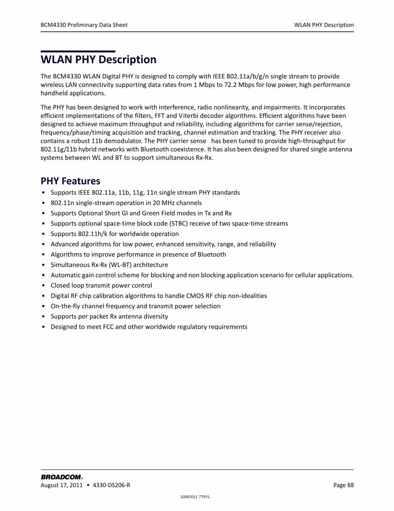
10/9/2011 7T5YL
WLAN PHY Description
BROADCOM August 17, 2011 • 4330-DS206-R Page 88
®
BCM4330 Preliminary Data Sheet
WLAN PHY DescriptionThe BCM4330 WLAN Digital PHY is designed to comply with IEEE 802.11a/b/g/n single stream to provide wireless LAN connectivity supporting data rates from 1 Mbps to 72.2 Mbps for low power, high performance handheld applications.
The PHY has been designed to work with interference, radio nonlinearity, and impairments. It incorporates efficient implementations of the filters, FFT and Viterbi decoder algorithms. Efficient algorithms have been designed to achieve maximum throughput and reliability, including algorithms for carrier sense/rejection, frequency/phase/timing acquisition and tracking, channel estimation and tracking. The PHY receiver also contains a robust 11b demodulator. The PHY carrier sense has been tuned to provide high-throughput for 802.11g/11b hybrid networks with Bluetooth coexistence. It has also been designed for shared single antenna systems between WL and BT to support simultaneous Rx-Rx.
PHY Features• Supports IEEE 802.11a, 11b, 11g, 11n single stream PHY standards
• 802.11n single-stream operation in 20 MHz channels
• Supports Optional Short GI and Green Field modes in Tx and Rx
• Supports optional space-time block code (STBC) receive of two space-time streams
• Supports 802.11h/k for worldwide operation
• Advanced algorithms for low power, enhanced sensitivity, range, and reliability
• Algorithms to improve performance in presence of Bluetooth
• Simultaneous Rx-Rx (WL-BT) architecture
• Automatic gain control scheme for blocking and non blocking application scenario for cellular applications.
• Closed loop transmit power control
• Digital RF chip calibration algorithms to handle CMOS RF chip non-idealities
• On-the-fly channel frequency and transmit power selection
• Supports per packet Rx antenna diversity
• Designed to meet FCC and other worldwide regulatory requirements
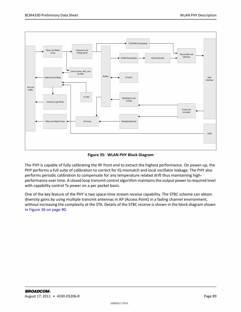
10/9/2011 7T5YL
WLAN PHY Description
BROADCOM August 17, 2011 • 4330-DS206-R Page 89
®
BCM4330 Preliminary Data Sheet
Figure 35: WLAN PHY Block Diagram
The PHY is capable of fully calibrating the RF front end to extract the highest performance. On power-up, the PHY performs a full suite of calibration to correct for IQ mismatch and local oscillator leakage. The PHY also performs periodic calibration to compensate for any temperature related drift thus maintaining high-performance over time. A closed loop transmit control algorithm maintains the output power to required level with capability control Tx power on a per packet basis.
One of the key feature of the PHY is two space-time stream receive capability. The STBC scheme can obtain diversity gains by using multiple transmit antennas in AP (Access Point) in a fading channel environment, without increasing the complexity at the STA. Details of the STBC receive is shown in the block diagram shown in Figure 36 on page 90.
Filters and Radio Comp
Frequency and Timing Synch
Carrier Sense, AGC, and Rx FSM
Radio Control Block
Common Logic Block
Filters and Radio Comp
AFE and Radio
MAC Interface
Buffers
OFDM Demodulate Viterbi Decoder
Tx FSM
PA Comp
Modulation and Coding
Modulate/Spread
Frame and Scramble
FFT/IFFT
CCK/DSSS Demodulate
Descramble and Deframe
COEX
10/9/2011 7T5YL
WLAN PHY Description
BROADCOM August 17, 2011 • 4330-DS206-R Page 90
®
BCM4330 Preliminary Data Sheet
Figure 36: STBC Receive Block Diagram
In STBC mode, symbols are processed in pairs. Equalized output symbols are linearly combined and decoded. Channel estimate is refined on every pair of symbols using the received symbols and reconstructed symbols.
Equalizer Demod Combine Demapper Viterbi
Channel h
SymbolMemory
Weighted Averaging
EstimateChannel
Transmitter
FFT of 2 SymbolsDescramble and
Deframe
hold
hupd
hnew

10/9/2011 7T5YL
WLAN Radio Subsystem
BROADCOM August 17, 2011 • 4330-DS206-R Page 91
®
BCM4330 Preliminary Data Sheet
Section 13: WLAN Radio Subsystem
The BCM4330 includes an integrated dual-band WLAN RF transceiver that has been optimized for use in 2.4 GHz and 5 GHz Wireless LAN systems (but not both simultaneously). It has been designed to provide low-power, low-cost, and robust communications for applications operating in the globally available 2.4 GHz unlicensed ISM or 5 GHz U-NII bands. The transmit and receive sections include all on-chip filtering, mixing, and gain control functions.
Up to eight RF control signals are available to drive the external RF switches and support the addition of optional external power amplifiers and low noise amplifiers for either or both bands. See the reference board schematics for further details.
Receive Path The BCM4330 has a wide dynamic range, direct conversion receiver. It employs high order on-chip channel filtering to ensure reliable operation in the noisy 2.4 GHz ISM band or the entire 5 GHz U-NII band. Control signals are available that can support the use of optional external low noise amplifiers (LNA), which can increase the receive sensitivity by several dB.
Transmit Path Baseband data is modulated and upconverted to the 2.4 GHz ISM or 5-GHz U-NII bands, respectively. Linear on-chip power amplifiers are included, which are capable of delivering high output powers while meeting 802.11a/b/g/n specifications without the need for external PAs.
These PAs can be powered directly from VBAT, thereby eliminating the need for a separate PALDO. Closed-loop output power control is completely integrated.
Several spare RF control signals are available to support the addition of optional external power amplifiers for either or both bands.
Calibration The BCM4330 features dynamic on-chip calibration, eliminating process variation across components. This enables the BCM4330 to be used in high-volume applications, because calibration routines are not required during manufacturing testing. These calibration routines are performed periodically in the course of normal radio operation. Examples of this automatic calibration are baseband filter calibration for optimum transmit and receive performance and LOFT calibration for leakage reduction. In addition, I/Q Calibration, R Calibration, and VCO Calibration are performed on-chip.
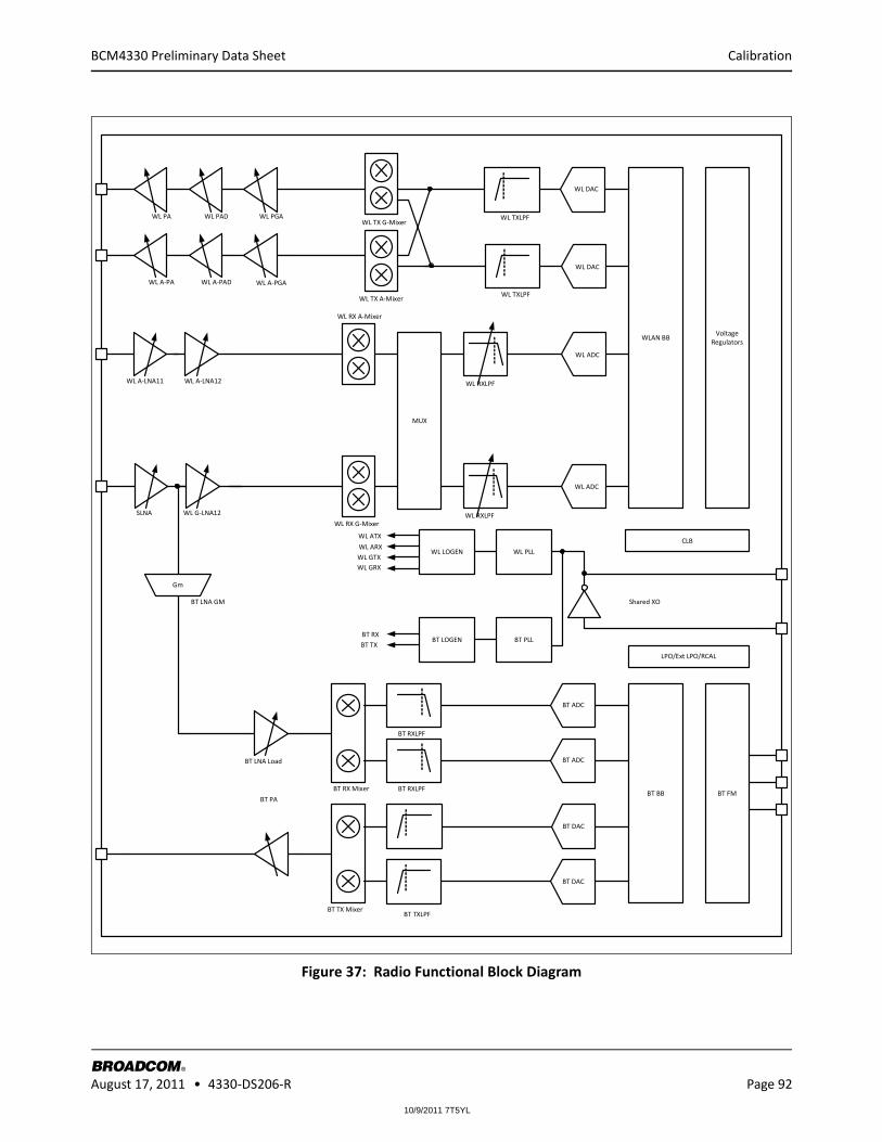
10/9/2011 7T5YL
Calibration
BROADCOM August 17, 2011 • 4330-DS206-R Page 92
®
BCM4330 Preliminary Data Sheet
Figure 37: Radio Functional Block Diagram
Gm
BT LOGEN
WL LOGEN
BT PLL
WL PLL
WLAN BB
BT BB
CLB
Voltage Regulators
BT FM
LPO/Ext LPO/RCAL
WL ADC
BT ADC
BT DAC
WL PA WL PAD WL PGAWL TX G-Mixer
WL DAC
WL A-PA WL A-PAD WL A-PGA
WL TX A-Mixer
WL TXLPF
WL RXLPF
WL RX A-Mixer
WL RX G-Mixer
WL A-LNA11 WL A-LNA12
SLNA WL G-LNA12
BT LNA Load
BT LNA GM
BT PA
BT RX Mixer
BT TX Mixer
BT RXLPF
BT TXLPF
Shared XO
WL TXLPF
WL DAC
WL ADC
WL RXLPF
WL ATX
WL GRXWL GTXWL ARX
MUX
BT TXBT RX
BT ADC
BT RXLPF
BT DAC

10/9/2011 7T5YL
Pinout and Signal Descriptions
BROADCOM August 17, 2011 • 4330-DS206-R Page 93
®
BCM4330 Preliminary Data Sheet
Section 14: Pinout and Signal Descriptions
Signal AssignmentsFigure 38 shows the FCFBGA ball map. Figure 39 shows the WLBGA ball map. Figure 40 shows the WLCSP bump map.
Table 17 on page 96 contains the WLCSP bump coordinates.
Table 18 on page 103 contains the signal description for all packages.
Figure 38: 144-FCFBGA Ball Map (Top View)
4321A WRF_VDDPA_5G WRF_VDDPA_2GB WRF_VDDLNA_1P2_5G WRF_GNDLNA_5G WRF_A_TSSI_IN WRF_GNDPA_5GC WRF_LOGEN_A_VDD1P2 WRF_LOGEN_A_GND WRF_ANA_GND WRF_PADRV_VDDD WRF_VDD_VCOLDO_IN_1P8 WRF_VDDANA_1P2 WRF_VCOLDO_OUT_1P2 WRF_GPIO_OUTE WRF_TCXO_VDD WRF_VCO_GND WRF_VDDAFE_1P2 WRF_RES_EXTF WRF_XTAL_OP WRF_TCXO_IN WRF_AFE_GND BT_PCM_ING WRF_XTAL_ON WRF_XTAL_GND WRF_XTAL_VDD1P2 WL_GPIO_4H WL_GPIO_1 WL_GPIO_0 WL_GPIO_2 WL_GPIO_6J CSSV3_OIPG_LWCDDV_LW21DDVA_CISHK HSIC_STROBE HSIC_AVSS RF_SW_CTRL_7 VDDIO_RFL HSIC_DATA HSIC_RREF RF_SW_CTRL_2 RF_SW_CTRL_4M RF_SW_CTRL_5 RF_SW_CTRL_1 RF_SW_CTRL_0 RF_SW_CTRL_6
8765
A WRF_RFOUT_2G WRF_RFIN_2G BT_PAVDD3P3 BT_RFB WRF_GNDPA_2G WRF_VDDLNA_1P2_2G BT_IFVDD1P2 BT_FEVSSC SSV_TBSSVFI_TBG2_ANLDNG_FRWDNG_VRDAP_FRWD WRF_G_TSSI_IN BT_UART_CTS_N BT_CLK_REQ_IN BT_CLK_REQ_POLE BT_PCM_CLK BT_UART_RXD BT_UART_TXD BT_CLK_REQ_MODEF CDDV_TBCDDV_LWN_STR_TRAU_TBCNYS_MCP_TBG CSSVCSSVCSSVTUO_MCP_TBH SW_S2I_TBOPLCDDV_LW5_OIPG_LWJ CDDV_TBOIDDV_TBCSSVCSSVK RF_SW_CTRL_3 WL_VDDIO VDD_ISLAND BT_VDDCL 3_ATAD_OIDS0_ATAD_OIDSCDDV_LWLES_GATJM SDIO_DATA_1 SDIO_CLK SDIO_CMD SDIO_DATA_2
2111019
A BT_LNAVDD1P2 BT_VCOVDD1P2 FM_AOUT1 FM_AOUT2B BT_RFVSS BT_PLLVDD1P2 FM_VDDAUDIO FM_TXC BT_VCOVSS FM_VSSAUDIO FM_IFVDD1P2 FM_RFVDD_1P2D BT_PLLVSS FM_PLLVSS FM_RFVSS FM_RXNE FM_VSS FM_VDD2P5 FM_VSSVCO FM_RXPF TUO_QER_KLC_TB0MT_TBN_TSR_TB0_OIPG_TBG BT_I2S_CLK BT_I2S_DI BT_GPIO_4 BT_GPIO_2H BT_I2S_DO BT_GPIO_5 BT_GPIO_1 BT_GPIO_3J EXT_SMPS_REQ EXT_PWM_REQ VOUT_3P1 VOUT_3P3K BT_REG_ON PMU_AVSS SR_VDDBAT2 SR_VDDBAT1L WL_REG_ON VOUT_LNLDO1 SR_VLX SR_VDDBAT1M XLV_RSSSVP_RSODL_NIVODLC_TUOV
WRF_RFOUT_5GWRF_RFIN_5G

10/9/2011 7T5YL
Signal Assignments
BROADCOM August 17, 2011 • 4330-DS206-R Page 94
®
BCM4330 Preliminary Data Sheet
Figure 39: 133-WLBGA Ball Map (bottom view)
FM_AOUT1BT_
VCOVDD1P2BT_FEVSS BT_RF
BT_PAVDD3P3
WRF_RFIN_2GWRF_
RFOUT_2GWRF_VDDPA
WRF_RFOUT_5G
123456789101112
A
B
C
D
E
F
G
H
J
K
L
M
A
B
C
D
E
F
G
H
J
K
L
M
FM_AOUT2BT_
PLLVDD1P2BT_RFVSS BT_RFVDD1P2 BT_IFVDD1P2
WRF_VDDLNA_1P2_2G
WRF_PA_GNDWRF_
PA_GNDWRF_PA_GND
WRF_RFIN_5G
FM_TXFM_
VSSAUDIOBT_PLLVSS BT_VSS BT_IFVSS
WRF_GNDLNA_2G
WRF_GNDWRF_PADRV_
GNDWRF_
PADRV_VDDWRF_
ANA_GND
FM_RXN FM_RXPFM_
VDDAUDIOBT_GPIO_1 WL_GPIO_6
BT_CLK_REQ_IN
BT_UART_TXD
WL_GPIO_3WRF_A_TSSI_IN
WRF_LOGEN_A
_GND
WRF_LOGEN_A_
VDD1P2
WRF_VDDANA_1P2
FM_RFVDD1P2
FM_RXVSSFM_
VDDPLL1P2
BT_CLK_REQ_
MODEBT_VDDC WL_VDDC BT_UART_RXD WL_VSS_2
WRF_GPIO_OUT
WRF_RES_EXTWRF_VDD_VCOLDO_IN_1P8
FM_VDD2P5 FM_VSSVCO FM_PLLVSS BT_GPIO_0 BT_VSSC BT_VDDIOBT_UART_
RTS_NJTAG_SEL
WRF_AFE_GND
WRF_TCXO_VDD
WRF_VCOLDO_OUT_1P2
WRF_VCO_GND
BT_CLK_REQ_OUT
BT_TM0 BT_RST_N BT_GPIO_7 BT_I2S_DIBT_UART_
CTS_NWL_GPIO_1
WRF_VDDAFE_1P2
WRF_TCXO_IN
WRF_XTAL_OP
BT_GPIO_4 BT_GPIO_2 BT_GPIO_3 BT_GPIO_6 BT_I2S_DO BT_PCM_CLK WL_GPIO_2 WL_GPIO_0WRF_
XTAL_VDD1P2
WRF_XTAL_GND
WRF_XTAL_ON
VOUT_3P3 VOUT_3P1EXT_PWM_
REQBT_GPIO_5 WL_GPIO_4 LPO BT_PCM_IN BT_PCM_OUT
RF_SW_CTRL_5
RF_SW_CTRL_6
RF_SW_CTRL_1
HSIC_RREF
SR_VDDBAT1 SR_VDDBAT2 BT_REG_ONEXT_SMPS_
REQBT_VDDC WL_VDDC
BT_PCM_SYNC
RF_SW_CTRL_0
RF_SW_CTRL_7
RF_SW_CTRL_4
WL_VSS_0 WL_VDDC
SR_VDDBAT1 PMU_AVSSVOUT_LNLDO1
WL_REG_ON SDIO_DATA_3 SDIO_CMD WL_GPIO_5 WL_VSS_1RF_SW_CTRL_2
VDDIO_RF HSIC_DATA HSIC_AVDD12
SR_VLX SR_PVSS VIN_LDO VOUT_CLDO SDIO_DATA_1 SDIO_CLK SDIO_DATA_0 SDIO_DATA_2RF_SW_CTRL_3
WL_VDDO HSIC_STROBE HSIC_AVSS
123456789101112

10/9/2011 7T5YL
Signal Assignments
BROADCOM August 17, 2011 • 4330-DS206-R Page 95
®
BCM4330 Preliminary Data Sheet
Figure 40: WLCSP 225-Bump Map (bottom view)

10/9/2011 7T5YL
Signal Assignments
BROADCOM August 17, 2011 • 4330-DS206-R Page 96
®
BCM4330 Preliminary Data Sheet
Table 17: WLCSP 225-Bump Coordinates
BumpNumber Signal
Bump Side View Top Side View
0,0 is in the Center of the Die
X Y X Y
1 WRF_A_TSSI_IN 2250 1490 –2250 1490
2 WRF_ANA_GND 955 1490 –955 1490
3 WRF_ANA_GND 2050 1490 –2050 1490
4 WRF_AFE_GND 1175 485 –1175 485
5 WRF_AFE_GND 1485 235 –1485 235
6 WRF_GNDLNA_2G –220 2270 220 2270
7 WRF_GNDLNA_5G 2050 2470 –2050 2470
8 WRF_LOGEN_A_GND 1995 1885 –1995 1885
9 WRF_PADRV_GND 955 1890 –955 1890
10 WRF_GNDPA_2G 400 2120 –400 2120
11 WRF_GNDPA_2G 1075 2050 –1075 2050
12 WRF_GNDPA_5G 1075 2250 –1075 2250
13 WRF_GNDPA_5G 1800 2120 –1800 2120
14 WRF_VCO_GND 2250 660 –2250 660
15 WRF_GPIO_OUT 2050 1040 –2050 1040
16 WRF_G_TSSI_IN 1175 1285 –1175 1285
17 WRF_RES_EXT 2250 1060 –2250 1060
18 WRF_RFIN_2G 128 2470 –128 2470
19 WRF_RFIN_5G 2250 2470 –2250 2470
20 WRF_RFOUT_2G 404 2470 –404 2470
21 WRF_RFOUT_5G 1693 2470 –1693 2470
22 WRF_VCOLDO_OUT_1P2 2050 660 –2050 660
23 WRF_VDDAFE_1P2 1175 685 –1175 685
24 WRF_VDDAFE_1P2 1285 235 –1285 235
25 WRF_VDDANA_1P2 1155 1490 –1155 1490
26 WRF_LOGEN_A_VDD1P2 2250 1260 –2250 1260
27 WRF_VDDLNA_1P2_2G –220 2470 220 2470
28 WRF_VDDLNA_1P2_5G 2100 2220 –2100 2220
29 WRF_VDDLO_1P2_5G 2235 1715 –2235 1715
30 WRF_PADRV_VDD 955 1690 –955 1690
31 WRF_VDDPA_2G 745 2470 –745 2470
32 WRF_VDDPA_2G 945 2470 –945 2470
33 WRF_VDDPA_5G 1145 2470 –1145 2470
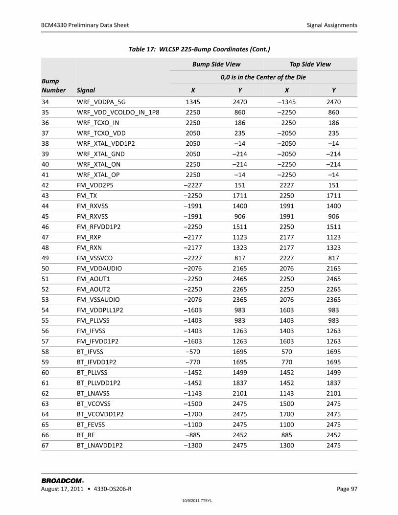
10/9/2011 7T5YL
Signal Assignments
BROADCOM August 17, 2011 • 4330-DS206-R Page 97
®
BCM4330 Preliminary Data Sheet
34 WRF_VDDPA_5G 1345 2470 –1345 2470
35 WRF_VDD_VCOLDO_IN_1P8 2250 860 –2250 860
36 WRF_TCXO_IN 2250 186 –2250 186
37 WRF_TCXO_VDD 2050 235 –2050 235
38 WRF_XTAL_VDD1P2 2050 –14 –2050 –14
39 WRF_XTAL_GND 2050 –214 –2050 –214
40 WRF_XTAL_ON 2250 –214 –2250 –214
41 WRF_XTAL_OP 2250 –14 –2250 –14
42 FM_VDD2P5 –2227 151 2227 151
43 FM_TX –2250 1711 2250 1711
44 FM_RXVSS –1991 1400 1991 1400
45 FM_RXVSS –1991 906 1991 906
46 FM_RFVDD1P2 –2250 1511 2250 1511
47 FM_RXP –2177 1123 2177 1123
48 FM_RXN –2177 1323 2177 1323
49 FM_VSSVCO –2227 817 2227 817
50 FM_VDDAUDIO –2076 2165 2076 2165
51 FM_AOUT1 –2250 2465 2250 2465
52 FM_AOUT2 –2250 2265 2250 2265
53 FM_VSSAUDIO –2076 2365 2076 2365
54 FM_VDDPLL1P2 –1603 983 1603 983
55 FM_PLLVSS –1403 983 1403 983
56 FM_IFVSS –1403 1263 1403 1263
57 FM_IFVDD1P2 –1603 1263 1603 1263
58 BT_IFVSS –570 1695 570 1695
59 BT_IFVDD1P2 –770 1695 770 1695
60 BT_PLLVSS –1452 1499 1452 1499
61 BT_PLLVDD1P2 –1452 1837 1452 1837
62 BT_LNAVSS –1143 2101 1143 2101
63 BT_VCOVSS –1500 2475 1500 2475
64 BT_VCOVDD1P2 –1700 2475 1700 2475
65 BT_FEVSS –1100 2475 1100 2475
66 BT_RF –885 2452 885 2452
67 BT_LNAVDD1P2 –1300 2475 1300 2475
Table 17: WLCSP 225-Bump Coordinates (Cont.)
BumpNumber Signal
Bump Side View Top Side View
0,0 is in the Center of the Die
X Y X Y
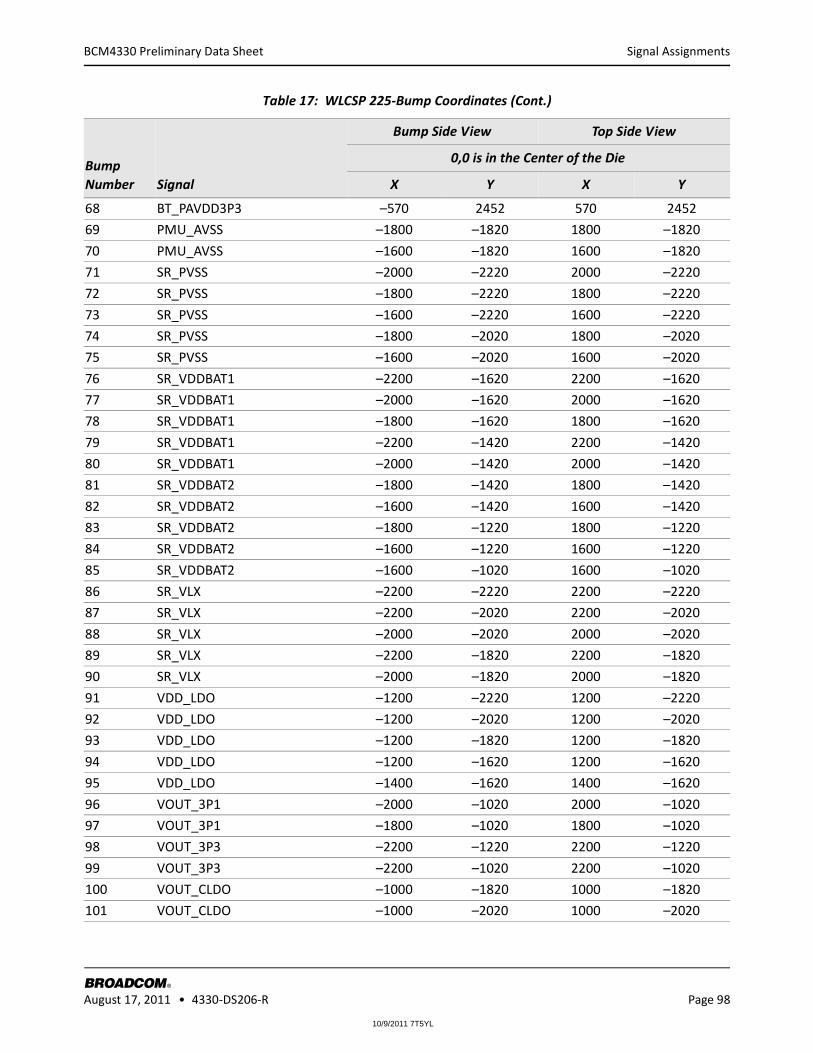
10/9/2011 7T5YL
Signal Assignments
BROADCOM August 17, 2011 • 4330-DS206-R Page 98
®
BCM4330 Preliminary Data Sheet
68 BT_PAVDD3P3 –570 2452 570 2452
69 PMU_AVSS –1800 –1820 1800 –1820
70 PMU_AVSS –1600 –1820 1600 –1820
71 SR_PVSS –2000 –2220 2000 –2220
72 SR_PVSS –1800 –2220 1800 –2220
73 SR_PVSS –1600 –2220 1600 –2220
74 SR_PVSS –1800 –2020 1800 –2020
75 SR_PVSS –1600 –2020 1600 –2020
76 SR_VDDBAT1 –2200 –1620 2200 –1620
77 SR_VDDBAT1 –2000 –1620 2000 –1620
78 SR_VDDBAT1 –1800 –1620 1800 –1620
79 SR_VDDBAT1 –2200 –1420 2200 –1420
80 SR_VDDBAT1 –2000 –1420 2000 –1420
81 SR_VDDBAT2 –1800 –1420 1800 –1420
82 SR_VDDBAT2 –1600 –1420 1600 –1420
83 SR_VDDBAT2 –1800 –1220 1800 –1220
84 SR_VDDBAT2 –1600 –1220 1600 –1220
85 SR_VDDBAT2 –1600 –1020 1600 –1020
86 SR_VLX –2200 –2220 2200 –2220
87 SR_VLX –2200 –2020 2200 –2020
88 SR_VLX –2000 –2020 2000 –2020
89 SR_VLX –2200 –1820 2200 –1820
90 SR_VLX –2000 –1820 2000 –1820
91 VDD_LDO –1200 –2220 1200 –2220
92 VDD_LDO –1200 –2020 1200 –2020
93 VDD_LDO –1200 –1820 1200 –1820
94 VDD_LDO –1200 –1620 1200 –1620
95 VDD_LDO –1400 –1620 1400 –1620
96 VOUT_3P1 –2000 –1020 2000 –1020
97 VOUT_3P1 –1800 –1020 1800 –1020
98 VOUT_3P3 –2200 –1220 2200 –1220
99 VOUT_3P3 –2200 –1020 2200 –1020
100 VOUT_CLDO –1000 –1820 1000 –1820
101 VOUT_CLDO –1000 –2020 1000 –2020
Table 17: WLCSP 225-Bump Coordinates (Cont.)
BumpNumber Signal
Bump Side View Top Side View
0,0 is in the Center of the Die
X Y X Y

10/9/2011 7T5YL
Signal Assignments
BROADCOM August 17, 2011 • 4330-DS206-R Page 99
®
BCM4330 Preliminary Data Sheet
102 VOUT_CLDO –1000 –2220 1000 –2220
103 VOUT_LNLDO1 –1400 –2220 1400 –2220
104 VOUT_LNLDO1 –1400 –2020 1400 –2020
105 VOUT_LNLDO1 –1400 –1820 1400 –1820
106 WL_REG_ON –1000 –1620 1000 –1620
107 BT_REG_ON –1400 –1420 1400 –1420
108 BT_REG_ON –1200 –1420 1200 –1420
109 EXT_PWM_REQ –1400 –1220 1400 –1220
110 EXT_PWM_REQ –1400 –1020 1400 –1020
111 EXT_SMPS_REQ –1200 –1220 1200 –1220
112 EXT_SMPS_REQ –1000 –1220 1000 –1220
113 BT_CLK_REQ_IN –600 1320 600 1320
114 BT_CLK_REQ_MODE –800 1080 800 1080
115 BT_GPIO_1 –2200 –320 2200 –320
116 BT_CLK_REQ_POL –800 1320 800 1320
117 BT_GPIO_0 –1250 –320 1250 –320
118 BT_CLK_REQ_OUT –2200 –120 2200 –120
119 BT_GPIO_2 –1800 –320 1800 –320
120 BT_GPIO_3 –2200 –520 2200 –520
121 BT_GPIO_4 –1800 –520 1800 –520
122 BT_GPIO_5 –1400 –560 1400 –560
123 BT_I2S_CLK –910 210 910 210
124 BT_I2S_DI –1350 –120 1350 –120
125 BT_I2S_DO –1010 –150 1010 –150
126 BT_I2S_WS –810 –200 810 –200
127 BT_PCM_CLK 350 500 –350 500
128 BT_PCM_IN 350 260 –350 260
129 BT_PCM_OUT 600 260 –600 260
130 BT_PCM_SYNC 600 500 –600 500
131 BT_RST_N –1550 –120 1550 –120
132 BT_TM1 –1750 –120 1750 –120
133 BT_TM0 –1950 –120 1950 –120
134 BT_UART_CTS_N –65 1205 65 1205
135 BT_UART_RTS_N 315 1205 –315 1205
Table 17: WLCSP 225-Bump Coordinates (Cont.)
BumpNumber Signal
Bump Side View Top Side View
0,0 is in the Center of the Die
X Y X Y

10/9/2011 7T5YL
Signal Assignments
BROADCOM August 17, 2011 • 4330-DS206-R Page 100
®
BCM4330 Preliminary Data Sheet
136 BT_UART_RXD 315 1005 –315 1005
137 BT_UART_TXD –65 1005 65 1005
138 BT_VDDC –800 840 800 840
139 BT_VDDC –1000 840 1000 840
140 BT_VDDC –1125 –710 1125 –710
141 BT_VDDC –800 –850 800 –850
142 BT_VDDC –600 840 600 840
143 BT_VDDC –900 –610 900 –610
144 BT_VDDC –650 –1050 650 –1050
145 BT_VDDC –650 –1250 650 –1250
146 BT_VDDC –450 –1000 450 –1000
147 BT_VDDC –450 –1200 450 –1200
148 BT_VDDC –1000 600 1000 600
149 BT_VDDIO –700 600 700 600
150 BT_VDDIO –600 245 600 245
151 BT_VSSC –600 –650 600 –650
152 BT_VSSC –600 1080 600 1080
153 BT_VSSC –600 45 600 45
154 BT_VSSC –425 –175 425 –175
155 BT_VSSC –400 1080 400 1080
156 BT_VSSC –400 840 400 840
157 BT_VSSC –500 600 500 600
158 BT_VSSC –400 45 400 45
159 BT_VSSC –400 –400 400 –400
160 HSIC_AVDD12 2000 –1835 –2000 –1835
161 HSIC_AVSS 2015 –1635 –2015 –1635
162 HSIC_DATA 2210 –2230 –2210 –2230
163 HSIC_RREF 2000 –2035 –2000 –2035
164 HSIC_STROBE 2210 –2030 –2210 –2030
165 JTAG_SEL 620 –2240 –620 –2240
166 LPO –400 –600 400 –600
167 RF_SW_CTRL_0 1735 –1505 –1735 –1505
168 RF_SW_CTRL_1 1735 –1705 –1735 –1705
169 RF_SW_CTRL_2 1785 –1905 –1785 –1905
Table 17: WLCSP 225-Bump Coordinates (Cont.)
BumpNumber Signal
Bump Side View Top Side View
0,0 is in the Center of the Die
X Y X Y
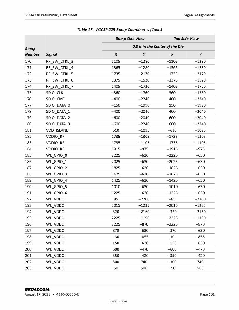
10/9/2011 7T5YL
Signal Assignments
BROADCOM August 17, 2011 • 4330-DS206-R Page 101
®
BCM4330 Preliminary Data Sheet
170 RF_SW_CTRL_3 1105 –1280 –1105 –1280
171 RF_SW_CTRL_4 1365 –1280 –1365 –1280
172 RF_SW_CTRL_5 1735 –2170 –1735 –2170
173 RF_SW_CTRL_6 1375 –1520 –1375 –1520
174 RF_SW_CTRL_7 1405 –1720 –1405 –1720
175 SDIO_CLK –360 –1760 360 –1760
176 SDIO_CMD –400 –2240 400 –2240
177 SDIO_DATA_0 –150 –1990 150 –1990
178 SDIO_DATA_1 –400 –2040 400 –2040
179 SDIO_DATA_2 –600 –2040 600 –2040
180 SDIO_DATA_3 –600 –2240 600 –2240
181 VDD_ISLAND 610 –1095 –610 –1095
182 VDDIO_RF 1735 –1305 –1735 –1305
183 VDDIO_RF 1735 –1105 –1735 –1105
184 VDDIO_RF 1915 –975 –1915 –975
185 WL_GPIO_0 2225 –630 –2225 –630
186 WL_GPIO_1 2025 –630 –2025 –630
187 WL_GPIO_2 1825 –630 –1825 –630
188 WL_GPIO_3 1625 –630 –1625 –630
189 WL_GPIO_4 1425 –630 –1425 –630
190 WL_GPIO_5 1010 –630 –1010 –630
191 WL_GPIO_6 1225 –630 –1225 –630
192 WL_VDDC 85 –2200 –85 –2200
193 WL_VDDC 2015 –1235 –2015 –1235
194 WL_VDDC 320 –2160 –320 –2160
195 WL_VDDC 2225 –1190 –2225 –1190
196 WL_VDDC 2225 –870 –2225 –870
197 WL_VDDC 370 –630 –370 –630
198 WL_VDDC –30 –855 30 –855
199 WL_VDDC 150 –630 –150 –630
200 WL_VDDC 600 –470 –600 –470
201 WL_VDDC 350 –420 –350 –420
202 WL_VDDC 300 740 –300 740
203 WL_VDDC 50 500 –50 500
Table 17: WLCSP 225-Bump Coordinates (Cont.)
BumpNumber Signal
Bump Side View Top Side View
0,0 is in the Center of the Die
X Y X Y
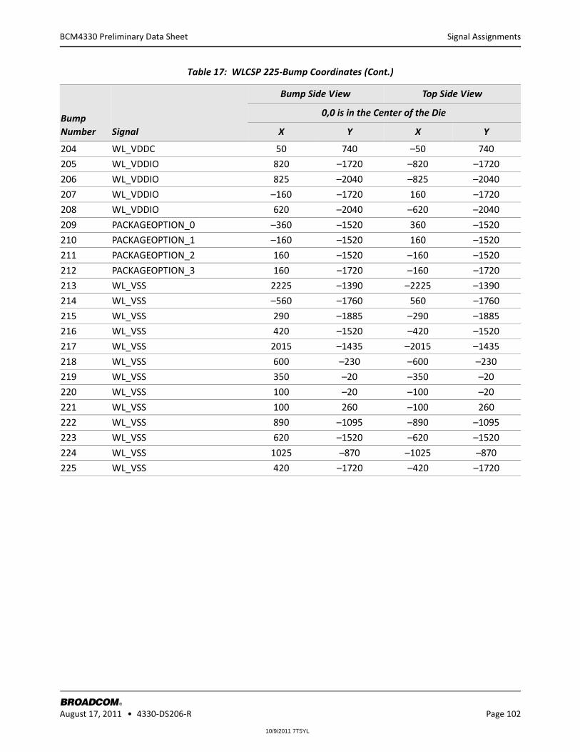
10/9/2011 7T5YL
Signal Assignments
BROADCOM August 17, 2011 • 4330-DS206-R Page 102
®
BCM4330 Preliminary Data Sheet
204 WL_VDDC 50 740 –50 740
205 WL_VDDIO 820 –1720 –820 –1720
206 WL_VDDIO 825 –2040 –825 –2040
207 WL_VDDIO –160 –1720 160 –1720
208 WL_VDDIO 620 –2040 –620 –2040
209 PACKAGEOPTION_0 –360 –1520 360 –1520
210 PACKAGEOPTION_1 –160 –1520 160 –1520
211 PACKAGEOPTION_2 160 –1520 –160 –1520
212 PACKAGEOPTION_3 160 –1720 –160 –1720
213 WL_VSS 2225 –1390 –2225 –1390
214 WL_VSS –560 –1760 560 –1760
215 WL_VSS 290 –1885 –290 –1885
216 WL_VSS 420 –1520 –420 –1520
217 WL_VSS 2015 –1435 –2015 –1435
218 WL_VSS 600 –230 –600 –230
219 WL_VSS 350 –20 –350 –20
220 WL_VSS 100 –20 –100 –20
221 WL_VSS 100 260 –100 260
222 WL_VSS 890 –1095 –890 –1095
223 WL_VSS 620 –1520 –620 –1520
224 WL_VSS 1025 –870 –1025 –870
225 WL_VSS 420 –1720 –420 –1720
Table 17: WLCSP 225-Bump Coordinates (Cont.)
BumpNumber Signal
Bump Side View Top Side View
0,0 is in the Center of the Die
X Y X Y
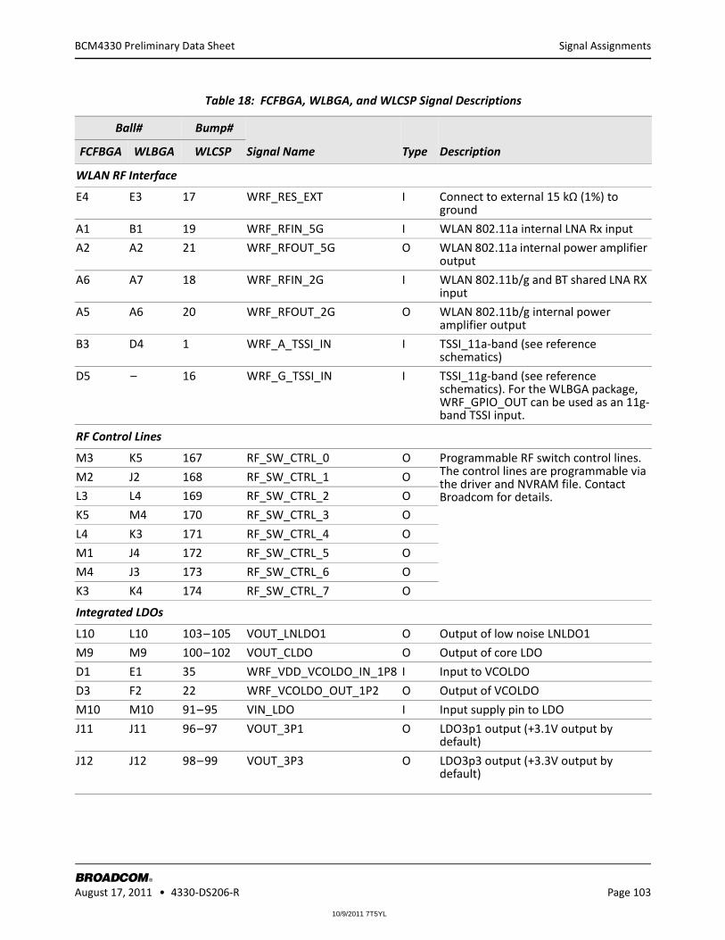
10/9/2011 7T5YL
Signal Assignments
BROADCOM August 17, 2011 • 4330-DS206-R Page 103
®
BCM4330 Preliminary Data Sheet
Table 18: FCFBGA, WLBGA, and WLCSP Signal Descriptions
Ball# Bump#
Signal Name Type DescriptionFCFBGA WLBGA WLCSP
WLAN RF Interface
E4 E3 17 WRF_RES_EXT I Connect to external 15 kΩ (1%) to ground
A1 B1 19 WRF_RFIN_5G I WLAN 802.11a internal LNA Rx input
A2 A2 21 WRF_RFOUT_5G O WLAN 802.11a internal power amplifier output
A6 A7 18 WRF_RFIN_2G I WLAN 802.11b/g and BT shared LNA RX input
A5 A6 20 WRF_RFOUT_2G O WLAN 802.11b/g internal power amplifier output
B3 D4 1 WRF_A_TSSI_IN I TSSI_11a-band (see reference schematics)
D5 – 16 WRF_G_TSSI_IN I TSSI_11g-band (see reference schematics). For the WLBGA package, WRF_GPIO_OUT can be used as an 11g-band TSSI input.
RF Control Lines
M3 K5 167 RF_SW_CTRL_0 O Programmable RF switch control lines. The control lines are programmable via the driver and NVRAM file. Contact Broadcom for details.
M2 J2 168 RF_SW_CTRL_1 O
L3 L4 169 RF_SW_CTRL_2 O
K5 M4 170 RF_SW_CTRL_3 O
L4 K3 171 RF_SW_CTRL_4 O
M1 J4 172 RF_SW_CTRL_5 O
M4 J3 173 RF_SW_CTRL_6 O
K3 K4 174 RF_SW_CTRL_7 O
Integrated LDOs
L10 L10 103 – 105 VOUT_LNLDO1 O Output of low noise LNLDO1
M9 M9 100 – 102 VOUT_CLDO O Output of core LDO
D1 E1 35 WRF_VDD_VCOLDO_IN_1P8 I Input to VCOLDO
D3 F2 22 WRF_VCOLDO_OUT_1P2 O Output of VCOLDO
M10 M10 91 – 95 VIN_LDO I Input supply pin to LDO
J11 J11 96 – 97 VOUT_3P1 O LDO3p1 output (+3.1V output by default)
J12 J12 98 – 99 VOUT_3P3 O LDO3p3 output (+3.3V output by default)
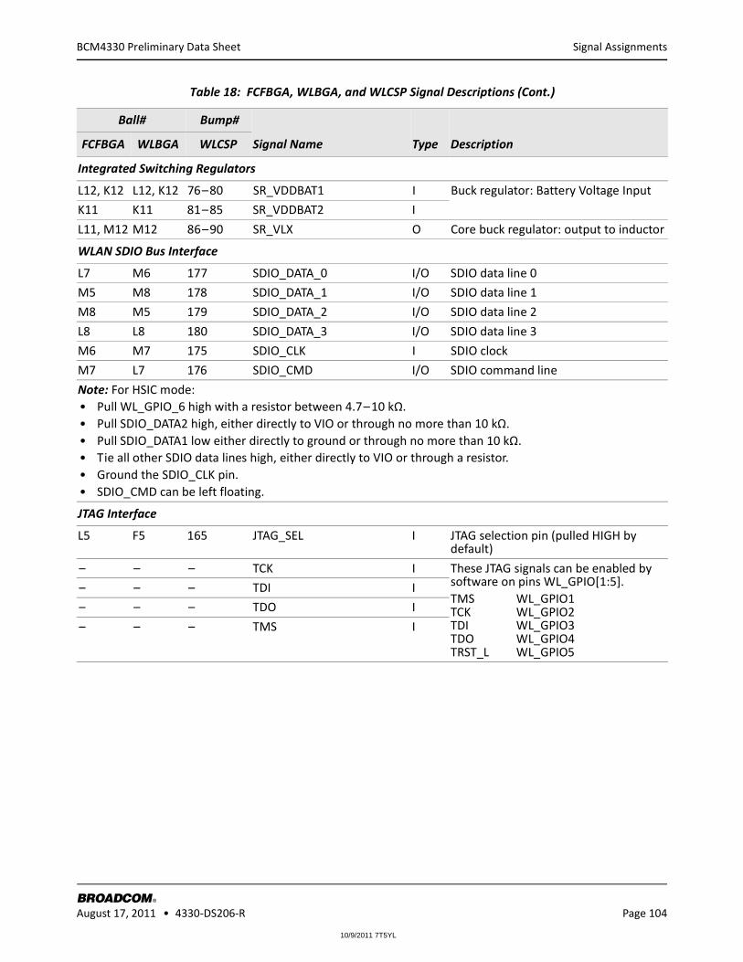
10/9/2011 7T5YL
Signal Assignments
BROADCOM August 17, 2011 • 4330-DS206-R Page 104
®
BCM4330 Preliminary Data Sheet
Integrated Switching Regulators
L12, K12 L12, K12 76 – 80 SR_VDDBAT1 I Buck regulator: Battery Voltage Input
K11 K11 81 – 85 SR_VDDBAT2 I
L11, M12 M12 86 – 90 SR_VLX O Core buck regulator: output to inductor
WLAN SDIO Bus Interface
L7 M6 177 SDIO_DATA_0 I/O SDIO data line 0
M5 M8 178 SDIO_DATA_1 I/O SDIO data line 1
M8 M5 179 SDIO_DATA_2 I/O SDIO data line 2
L8 L8 180 SDIO_DATA_3 I/O SDIO data line 3
M6 M7 175 SDIO_CLK I SDIO clock
M7 L7 176 SDIO_CMD I/O SDIO command line
Note: For HSIC mode:• Pull WL_GPIO_6 high with a resistor between 4.7 – 10 kΩ.• Pull SDIO_DATA2 high, either directly to VIO or through no more than 10 kΩ.• Pull SDIO_DATA1 low either directly to ground or through no more than 10 kΩ.• Tie all other SDIO data lines high, either directly to VIO or through a resistor.• Ground the SDIO_CLK pin.• SDIO_CMD can be left floating.
JTAG Interface
L5 F5 165 JTAG_SEL I JTAG selection pin (pulled HIGH by default)
– – – TCK I These JTAG signals can be enabled by software on pins WL_GPIO[1:5].TMS WL_GPIO1 TCK WL_GPIO2 TDI WL_GPIO3 TDO WL_GPIO4 TRST_L WL_GPIO5
– – – TDI I
– – – TDO I
– – – TMS I
Table 18: FCFBGA, WLBGA, and WLCSP Signal Descriptions (Cont.)
Ball# Bump#
Signal Name Type DescriptionFCFBGA WLBGA WLCSP

10/9/2011 7T5YL
Signal Assignments
BROADCOM August 17, 2011 • 4330-DS206-R Page 105
®
BCM4330 Preliminary Data Sheet
HSIC Interface
K1 M2 164 HSIC_STROBE I/O HSIC bidirectional data strobe signal. HSIC terminations are built in, external resistors are not needed. On SDIO designs this pin should not be connected.
L1 L2 162 HSIC_DATA I/O HSIC bidirectional DDR data signal. HSIC terminations are built in, external resistors are not needed. On SDIO designs this pin should not be connected.
L2 J1 163 HSIC_RREF I HSIC bias pin. Connect to ground via a 49.9 Ohm series resistor. On SDIO designs this pin should not be connected.
Clocks
F1 G1 41 WRF_XTAL_OP I Crystal oscillator input
G1 H1 40 WRF_XTAL_ON O Crystal oscillator output
F2 G3 36 WRF_TCXO_IN I External TCXO input
H7 J7 166 LPO I Input for external low-power clock
Table 18: FCFBGA, WLBGA, and WLCSP Signal Descriptions (Cont.)
Ball# Bump#
Signal Name Type DescriptionFCFBGA WLBGA WLCSP

10/9/2011 7T5YL
Signal Assignments
BROADCOM August 17, 2011 • 4330-DS206-R Page 106
®
BCM4330 Preliminary Data Sheet
WLAN GPIO
D4 E4 15 WRF_GPIO_OUT O Auxiliary RF I/O (see reference schematics). For the WLBGA package, WRF_GPIO_OUT can be used as an 11g-band TSSI signal.
H2 H4 185 WL_GPIO_0 I/O WLAN general interface pins. These pins are high-impedance on power up and reset. Subsequently, they become inputs or outputs through software control. These pins have programmable pull-up/down.WL_GPIO_0 may be configured by software to function as SDIO_Host_Wake.WL_GPIO[1:5] may be enabled as JTAG signals (see“JTAG Interface” on page 71).WL_GPIO[3:4] may be configured by software to function as UART_RX and UART_TX. WL_GPIO[1:5] can be configured as external coexistence interface pins (see “External Coexistence Interface” on page 71). For HSIC mode pull WL_GPIO_6 high with a resistor between 4.7 – 10 kΩ.
H1 G5 186 WL_GPIO_1 I/O
H3 H5 187 WL_GPIO_2 I/O
J3 D5 188 WL_GPIO_3 I/O
G4 J8 189 WL_GPIO_4 I/O
H5 L6 190 WL_GPIO_5 I/O
H4 D8 191 WL_GPIO_6 I/O
FM Transceiver
A11 A12 51 FM_AOUT1 O FM analog audio output channel 1
A12 B12 52 FM_AOUT2 O FM analog audio output channel 2
B12 C12 43 FM_TX O FM radio RF output antenna port
E12 D11 47 FM_RXP I FM radio RF antenna port
D12 D12 48 FM_RXN I FM radio RF antenna port
Bluetooth UART
E6 E6 136 BT_UART_RXD I/O Bluetooth UART signal input. Serial data input for the HCI UART Interface.
E7 D6 137 BT_UART_TXD I/O Bluetooth UART signal output. Serial data input for the HCI UART Interface.
F6 F6 135 BT_UART_RTS_N I/O Bluetooth UART REquest to Send. Active-low request-to-send signal for the HCI UART interface.
D6 G6 134 BT_UART_CTS_N I/O Bluetooth UART Clear to Send. Active-low clear-to-send signal for the HCI UART interface.
Table 18: FCFBGA, WLBGA, and WLCSP Signal Descriptions (Cont.)
Ball# Bump#
Signal Name Type DescriptionFCFBGA WLBGA WLCSP

10/9/2011 7T5YL
Signal Assignments
BROADCOM August 17, 2011 • 4330-DS206-R Page 107
®
BCM4330 Preliminary Data Sheet
Bluetooth Test Mode
F11 G11 133 BT_TM0 I Bluetooth test mode pin (no connect)
– – 132 BT_TM1 I Bluetooth test mode pin (no connect)
Bluetooth
A8 A9 66 BT_RF O Bluetooth PA output
D7 D7 113 BT_CLK_REQ_IN I Reference clock request
D8 – 116 BT_CLK_REQ_POL I BT Request clock power on reset
E8 E9 114 BT_CLK_REQ_MODE I External reference clock request mode.Pull this pin high to enable the BT_CLK_REQ_OUT signal to function as a high-asserting enable and disable control for an external TCXO.Pull this pin low if an external BT_CLK_REQ_OUT signal is not required; for example, if a dedicated crystal is used for the BCM4330. In this case, the crystal oscillator circuit is enabled and disabled internally.
F12 G12 118 BT_CLK_REQ_OUT O If enabled by the BT_CLK_REQ_MODE pin, this pin is the Bluetooth clock request output signal. See Table 4: “Power Control Pin Descriptions,” on page 43 for more information.
Bluetooth/FM I2S
G9 H8 123 BT_I2S_CLK I Bluetooth I2S pins
G10 G7 124 BT_I2S_DI I/O
H8 G8 126 BT_I2S_WS I/O
H9 H7 125 BT_I2S_DO I/O
Bluetooth PCM
E5 H6 127 BT_PCM_CLK I/O PCM clock, can be master (output) or slave (input)
F4 J6 128 BT_PCM_IN I/O PCM data input
G5 J5 129 BT_PCM_OUT I/O PCM data output
F5 K6 130 BT_PCM_SYNC I/O PCM sync signal, can be master (output) or slave (input)
Table 18: FCFBGA, WLBGA, and WLCSP Signal Descriptions (Cont.)
Ball# Bump#
Signal Name Type DescriptionFCFBGA WLBGA WLCSP
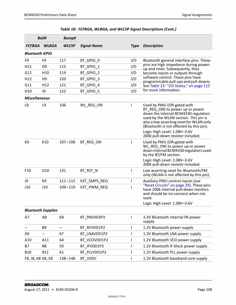
10/9/2011 7T5YL
Signal Assignments
BROADCOM August 17, 2011 • 4330-DS206-R Page 108
®
BCM4330 Preliminary Data Sheet
Bluetooth GPIO
F9 F9 117 BT_GPIO_0 I/O Bluetooth general interface pins. These pins are high impedance during power-up and reset. Subsequently, they become inputs or outputs through software control. These pins have programmable pull-ups and pull-downs. See Table 23: “I/O States,” on page 115 for more information.
H11 D9 115 BT_GPIO_1 I/O
G12 H10 119 BT_GPIO_2 I/O
H12 H9 120 BT_GPIO_3 I/O
G11 H12 121 BT_GPIO_4 I/O
H10 J9 122 BT_GPIO_5 I/O
Miscellaneous
L9 L9 106 WL_REG_ON I Used by PMU (OR-gated with BT_REG_ON) to power up or power down the internal BCM4330 regulators used by the WLAN section. This pin is also a low-asserting reset for WLAN only (Bluetooth is not affected by this pin).Logic High Level: 1.08V–3.6V 200k pull-down resistor included.
K9 K10 107 – 108 BT_REG_ON I Used by PMU (OR-gated with WL_REG_ON) to power up or power down internal BCM4330 regulators used by the BT/FM section.Logic High Level: 1.08V–3.6V 200k pull-down resistor included.
F10 G10 131 BT_RST_N I Low asserting reset for Bluetooth/FM only (WLAN is not affected by this pin).
J9 K9 111 – 112 EXT_SMPS_REQ I Auxiliary PMU control inputs (see “Reset Circuits” on page 29). These pins have 200k internal pull-down resistors and should be no-connect when not used.Logic High Level: 1.08V–3.6V
J10 J10 109 – 110 EXT_PWM_REQ I
Bluetooth Supplies
A7 A8 68 BT_PAVDD3P3 I 3.3V Bluetooth internal PA power supply
– B9 – BT_RFVDD1P2 I 1.2V Bluetooth power supply
A9 – 67 BT_LNAVDD1P2 I 1.2V Bluetooth LNA power supply
A10 A11 64 BT_VCOVDD1P2 I 1.2V Bluetooth VCO power supply
B7 B8 59 BT_IFVDD1P2 I 1.2V Bluetooth IF block power supply
B10 B11 61 BT_PLLVDD1P2 I 1.2V Bluetooth PLL power supply
F8, J8, K8 K8, E8 138 – 148 BT_VDDC I 1.2V Bluetooth baseband core supply
Table 18: FCFBGA, WLBGA, and WLCSP Signal Descriptions (Cont.)
Ball# Bump#
Signal Name Type DescriptionFCFBGA WLBGA WLCSP

10/9/2011 7T5YL
Signal Assignments
BROADCOM August 17, 2011 • 4330-DS206-R Page 109
®
BCM4330 Preliminary Data Sheet
WLAN Supplies
A3 – 33, 34 WRF_VDDPA_5G I VDD power supply (from VBAT) for the internal 11a-band power amplifier
A4 – 31, 32 WRF_VDDPA_2G I VDD power supply (from VBAT) for the internal 11g-band power amplifier
– A4 – WRF_VDDPA I VDD power supply (from VBAT) for both internal power amplifiers
C4 C3 30 WRF_PADRV_VDD I VDD power supply (from VBAT) supply for the WLAN PA driver
B1 – 28 WRF_VDDLNA_1P2_5G I 1.2V supply for the 11a-band internal LNA. If the IEEE 802.11a band is not used, tie this supply pin to WRF_VDDLNA_1P2_2G.
B6 B7 27 WRF_VDDLNA_1P2_2G I 1.2V supply for the 11g-band internal LNA
G3 H3 38 WRF_XTAL_VDD1P2 I 1.2V supply for the crystal oscillator circuit
E1 F3 37 WRF_TCXO_VDD I 1.7V to 3.3V supply for the BCM4330 TCXO driver. To maintain a constant load on the WRF_TCXO_IN pin (even when power is removed from the BCM4330), connect this supply pin to a 1.7V to 3.3V supply that is always present. If not used, this pin must be connected to ground (see Section 3: “Frequency References,” on page 30).
C1 D2 29 WRF_LOGEN_A_VDD1P2 I 1.2V supply for WLAN PLL
E3 G4 23, 24 WRF_VDDAFE_1P2 I 1.2V supply for WLAN AFE
D2 D1 25 – 26 WRF_VDDANA_1P2 I 1.2V supply for WLAN ADC/DAC block
F7, H6, J2, L6
E7,K7,K1 192–204 WL_VDDC I 1.2V supply for WLAN core
FM Transceiver Supplies
C12 E12 46 FM_RFVDD1P2 I 1.2V FM transceiver power supply
C11 – 57 FM_IFVDD1P2 I 1.2V FM IF power supply
– E10 54 FM_VDDPLL1P2 I 1.2V FM PLL power supply
E10 F12 42 FM_VDD2P5 I FM power supply (nominal 3.1V)
B11 D10 50 FM_VDDAUDIO I FM audio power supply
Table 18: FCFBGA, WLBGA, and WLCSP Signal Descriptions (Cont.)
Ball# Bump#
Signal Name Type DescriptionFCFBGA WLBGA WLCSP
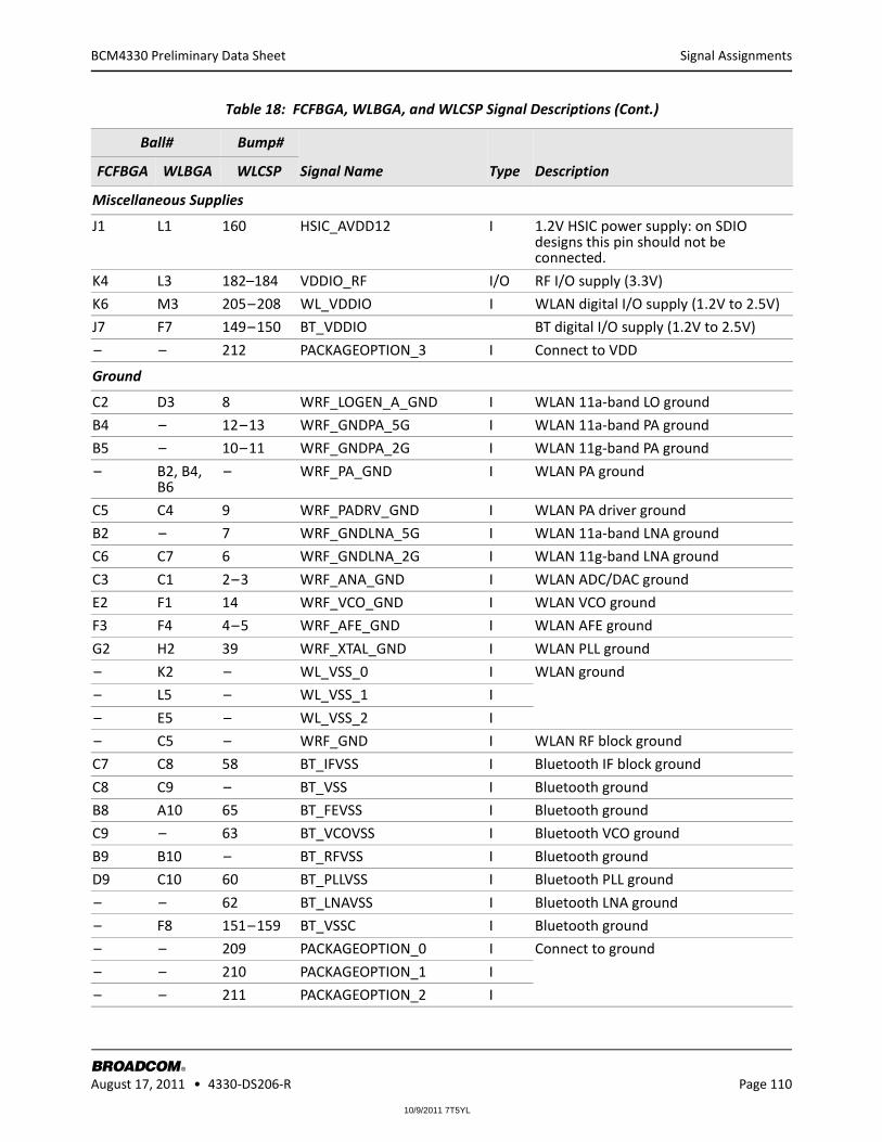
10/9/2011 7T5YL
Signal Assignments
BROADCOM August 17, 2011 • 4330-DS206-R Page 110
®
BCM4330 Preliminary Data Sheet
Miscellaneous Supplies
J1 L1 160 HSIC_AVDD12 I 1.2V HSIC power supply: on SDIO designs this pin should not be connected.
K4 L3 182–184 VDDIO_RF I/O RF I/O supply (3.3V)
K6 M3 205 – 208 WL_VDDIO I WLAN digital I/O supply (1.2V to 2.5V)
J7 F7 149 – 150 BT_VDDIO BT digital I/O supply (1.2V to 2.5V)
– – 212 PACKAGEOPTION_3 I Connect to VDD
Ground
C2 D3 8 WRF_LOGEN_A_GND I WLAN 11a-band LO ground
B4 – 12 – 13 WRF_GNDPA_5G I WLAN 11a-band PA ground
B5 – 10 – 11 WRF_GNDPA_2G I WLAN 11g-band PA ground
– B2, B4, B6
– WRF_PA_GND I WLAN PA ground
C5 C4 9 WRF_PADRV_GND I WLAN PA driver ground
B2 – 7 WRF_GNDLNA_5G I WLAN 11a-band LNA ground
C6 C7 6 WRF_GNDLNA_2G I WLAN 11g-band LNA ground
C3 C1 2 – 3 WRF_ANA_GND I WLAN ADC/DAC ground
E2 F1 14 WRF_VCO_GND I WLAN VCO ground
F3 F4 4 – 5 WRF_AFE_GND I WLAN AFE ground
G2 H2 39 WRF_XTAL_GND I WLAN PLL ground
– K2 – WL_VSS_0 I WLAN ground
– L5 – WL_VSS_1 I
– E5 – WL_VSS_2 I
– C5 – WRF_GND I WLAN RF block ground
C7 C8 58 BT_IFVSS I Bluetooth IF block ground
C8 C9 – BT_VSS I Bluetooth ground
B8 A10 65 BT_FEVSS I Bluetooth ground
C9 – 63 BT_VCOVSS I Bluetooth VCO ground
B9 B10 – BT_RFVSS I Bluetooth ground
D9 C10 60 BT_PLLVSS I Bluetooth PLL ground
– – 62 BT_LNAVSS I Bluetooth LNA ground
– F8 151 – 159 BT_VSSC I Bluetooth ground
– – 209 PACKAGEOPTION_0 I Connect to ground
– – 210 PACKAGEOPTION_1 I
– – 211 PACKAGEOPTION_2 I
Table 18: FCFBGA, WLBGA, and WLCSP Signal Descriptions (Cont.)
Ball# Bump#
Signal Name Type DescriptionFCFBGA WLBGA WLCSP
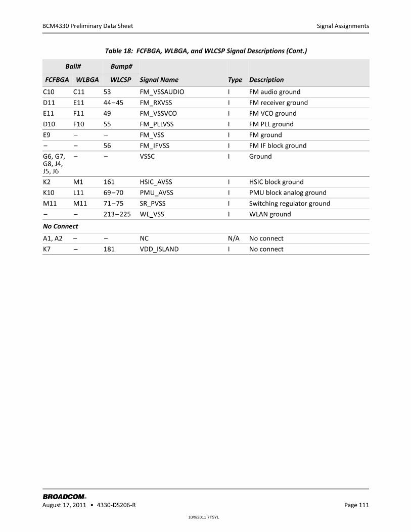
10/9/2011 7T5YL
Signal Assignments
BROADCOM August 17, 2011 • 4330-DS206-R Page 111
®
BCM4330 Preliminary Data Sheet
C10 C11 53 FM_VSSAUDIO I FM audio ground
D11 E11 44 – 45 FM_RXVSS I FM receiver ground
E11 F11 49 FM_VSSVCO I FM VCO ground
D10 F10 55 FM_PLLVSS I FM PLL ground
E9 – – FM_VSS I FM ground
– – 56 FM_IFVSS I FM IF block ground
G6, G7, G8, J4, J5, J6
– – VSSC I Ground
K2 M1 161 HSIC_AVSS I HSIC block ground
K10 L11 69 – 70 PMU_AVSS I PMU block analog ground
M11 M11 71 – 75 SR_PVSS I Switching regulator ground
– – 213 – 225 WL_VSS I WLAN ground
No Connect
A1, A2 – – NC N/A No connect
K7 – 181 VDD_ISLAND I No connect
Table 18: FCFBGA, WLBGA, and WLCSP Signal Descriptions (Cont.)
Ball# Bump#
Signal Name Type DescriptionFCFBGA WLBGA WLCSP

10/9/2011 7T5YL
Signal Assignments
BROADCOM August 17, 2011 • 4330-DS206-R Page 112
®
BCM4330 Preliminary Data Sheet
WLAN GPIO Signals and Strapping OptionsThe pins listed in Table 19 are sampled at power-on reset (POR) to determine the various operating modes. Sampling occurs a few milliseconds after an internal POR or deassertion of the external POR. After the POR, each pin assumes the GPIO or alternative function specified in the signal descriptions table. Each strapping option pin has an internal pull-up (PU) or pull-down (PD) resistor that determines the default mode. To change the mode, connect an external PU resistor to VDDIO or a PD resistor to GND, using a 10 kΩ resistor or less.
Note: Refer to the reference board schematics for more information.
Table 19: WLAN GPIO Functions and Strapping Options
Pin NameFCFBGA Pin #
WLBGA Pin #
WLCSP Pin # Default Function Description
SDIO_DATA_1 M5 M8 179 X strap_host_ifc_1 The three pins strap_host_ifc_[3:1] together select the host interface mode:• 0XX: SDIO• 10X: gSPI• 110: normal HSIC• 111: bootloader-less HSIC
SDIO_DATA_2 M8 M5 180 X strap_host_ifc_2
WL_GPIO_6 H4 D8 181 0 strap_host_ifc_3
Note: For HSIC mode:• Pull WL_GPIO_6 high with a resistor between 4.7 – 10 kΩ.• Pull SDIO_DATA2 high, either directly to VIO or through no more than 10 kΩ.• Pull SDIO_DATA1 low, either directly to ground or through no more than 10 kΩ.• Tie all other SDIO data lines high, either directly to VIO or through a resistor.• Ground the SDIO_CLK pin.• SDIO_CMD can be left floating.
Table 20: Strap Options
strap_host_ifc_3WL_GPIO_6
strap_host_ifc_2SDIO_DATA_2
strap_host_ifc_1SDIO_DATA_1
Default states at sampling instant 0 Float Float
SDIO 0 x x
gSPI 1 0 x
HSIC (normal) 1 1 0
Bootloader-less HSIC (debug only) 1 1 1

10/9/2011 7T5YL
Signal Assignments
BROADCOM August 17, 2011 • 4330-DS206-R Page 113
®
BCM4330 Preliminary Data Sheet
Muxed Bluetooth GPIO SignalsThe Bluetooth GPIO pins (BT_GPIO_0 to BT_GPIO_7) are multiplexed pins and can be programmed to be used as GPIOs or for other Bluetooth interface signals such as I2S. The specific function for a given BT_GPIO_X pin is chosen by programming the Pad Function Control Register for that specific pin. Table 21 shows the possible options for each BT_GPIO_X pin. Note that each BT_GPIO_X pin's Pad Function Control Register Setting is independent (i.e. BT_GPIO_1 can be set to Pad Function 7 at the same time that BT_GPIO_3 is set to PAD Function 0). When the Pad Function Control Register is set to 0 the BT_GPIOs do not have specific functions assigned to them and behave as generic GPIOs. The A_GPIO_X pins described below are multiplexed behind the BCM4330 PCM and I2S interface pins.
Table 21: GPIO Multiplexing Matrix
Pin Name
Pad Function Control Register Setting
0 1 2 3 4 5 6 7
BT_UART_CTS_N UART_CTS_N – – – – – – A_GPIO[1]
BT_UART_RTS_N UART_RTS_N – – – – – – A_GPIO[0]
BT_UART_RXD UART_RXD – – – – – – GPIO[5]
BT_UART_TXD UART_TXD – – – – – – GPIO[4]
BT_PCM_IN A_GPIO[3] PCM_IN PCM_IN HCLK – – – I2S_SSDI/MSDI
BT_PCM_OUT A_GPIO[2] PCM_OUT PCM_OUT LINK_IND – I2S_MSDO – I2S_SSDO
BT_PCM_SYNC A_GPIO[1] PCM_SYNC PCM_SYNC HCLK INT_LPO I2S_MWS – I2S_SWS
BT_PCM_CLK A_GPIO[0] PCM_CLK PCM_CLK – – I2S_MSCK – I2S_SSCK
BT_I2S_DO A_GPIO[5] PCM_OUT – – I2S_SSDO I2S_MSDO – STATUS
BT_2S_DI A_GPIO[6] PCM_IN – HCLK I2S_SSDI/MSDI
– – TX_CON_FX
BT_I2S_WS GPIO[7] PCM_SYNC – LINK_IND – I2S_MWS – I2S_SWS
BT_I2S_CLK GPIO[6] PCM_CLK – – INT_LPO I2S_MSCK – I2S_SSCK
BT_GPIO_5 GPIO[5] HCLK – I2S_MSCK I2S_SSCK – – CLK_REQ
BT_GPIO_4 GPIO[4] LINK_IND – I2S_MSDO I2S_SSDO – – –
BT_GPIO_3 GPIO[3] – – I2S_MWS I2S_SWS – – –
BT_GPIO_2 GPIO[2] – – – I2S_SSDI/MSDI
– – –
BT_GPIO_1 GPIO[1] – – – – – – –
BT_GPIO_0 GPIO[0] – – – clk_12p288 – – RF_ACTIVE
BT_CLK_REQ_IN A_GPIO[4] – – – – – – A_GPIO[4]
BT_CLK_REQ_OUT WL/BT_CLK_REQ – – – – – – A_GPIO[7]

10/9/2011 7T5YL
Signal Assignments
BROADCOM August 17, 2011 • 4330-DS206-R Page 114
®
BCM4330 Preliminary Data Sheet
The multiplexed GPIO signals are described in Table 22.
Table 22: Multiplexed GPIO Signals
Pin Name Type Description
UART_CTS_N I Host UART clear to send
UART_RTS_N O Device UART request to send
UART_RXD I Device UART receive data
UART_TXD O Host UART transmit data
PCM_IN I PCM data input
PCM_OUT O PCM data output
PCM_SYNC I/O PCM sync signal, can be master (output) or slave (input)
PCM_CLK I/O PCM clock, can be master (output) or slave (input)
GPIO[7:0] I/O General purpose I/O
A_GPIO[7:0] I/O A group general purpose I/O
I2S_MSDO O I2S master data output
I2S_MWS O I2S master word select
I2S_MSCK O I2S master clock
I2S_SSCK I I2S slave clock
I2S_SSDO O I2S slave data output
I2S_SWS I I2S slave word select
I2S_SSDI/MSDI I I2S slave/master data input
STATUS O Signals Bluetooth priority status
TX_CON_FX I WLAN-BT coexist. Transmission confirmation; permission for BT to transmit
RF_ACTIVE O WLAN-BT coexist. Asserted (logic high) during local BT RX and TX slots
LINK_IND O BT receiver/transmitter link indicator
WL/BT_CLK_REQ O WLAN clock request output

10/9/2011 7T5Y
L
BROADCOM August 17, 2011 • 4330-DS206-R Page 115
®
Signal AssignmentsBCM4330 Preliminary Data Sheet
I/O StatesThe following notations are used in Table 23:
• I: Input signal
• O: Output signal
• I/O: Input/Output signal
• PU = Pulled up
• PD = Pulled down
• NoPull = Neither pulled up nor pulled down
Table 23: I/O States
Name I/O Keepera Active ModeLow Power State/Sleep (all power present)
Power Downb (BT_REG_ON and WL_REG_ON held low)
Out of Reset; Before SW Download (BT_RST_N high; xx_REG_ON high)
(xx_REG_ON-high and BT_RST_N = 0) and VDDIOs are Present Power Rail
WL_REG_ON I N I; PD (pull down can be disabled)
I; PD (pull down can be disabled)
I; PD (of 200K) I; PD (of 200K) I; PD (of 200K) –
BT_RST_N I Y I; NoPull I; NoPull I; NoPull I; NoPull I; NoPull BT_VDDIO
BT_REG_ON I N I; PD (pull down can be disabled)
I; PD (pull down can be disabled)
I; PD (of 200K) I; PD (of 200K) I; PD (of 200K) –
BT_GPIO 0,1,2,3,4,5
I/O Y I/O; PU, PD, NoPull (programmable)
I/O; PU, PD, NoPull (programmable)
High-Z, NoPull I, PD I, PD BT_VDDIO
BT_UART_CTS I Y I; NoPull I; NoPull High-Z, NoPull I; PU I; PU BT_VDDIO
BT_UART_RTS O Y O; NoPull O; NoPull High-Z, NoPull I; PU I; PU BT_VDDIO
BT_UART_RXD I Y I; NoPull I; NoPull High-Z, NoPull I; PU I; PU BT_VDDIO
BT_UART_TXD O Y O; NoPull O; NoPull High-Z, NoPull I; PU I; PU BT_VDDIO
SDIO Datac I/O N I/O; PU I; PU High-Z, NoPull I; PU I; PU WL_VDDIO
SDIO CMDc I/O N I/O; PU I; PU High-Z, NoPull I; PU I; PU WL_VDDIO
SDIO_CLKc I N I; NoPull I; NoPull High-Z, NoPull I; NoPull I; NoPull WL_VDDIO
BT_PCM_CLK I/O Y I; NoPulld I; NoPulld High-Z, NoPull I, PD I, PD BT_VDDIO
BT_PCM_IN I/O Y I; NoPulld I; NoPulld High-Z, NoPull I, PD I, PD BT_VDDIO
BT_PCM_OUT I/O Y I; NoPulld I; NoPulld High-Z, NoPull I, PD I, PD BT_VDDIO

10/9/2011 7T5Y
L
BROADCOM August 17, 2011 • 4330-DS206-R Page 116
®
Signal AssignmentsBCM4330 Preliminary Data Sheet
BT_PCM_SYNC I/O Y I; NoPulld I; NoPulld High-Z, NoPull I, PD I, PD BT_VDDIO
BT_I2S_WS I/O Y I; NoPulle I; NoPulle High-Z, NoPull I, PD I, PD BT_VDDIO
BT_I2S_CLK I/O Y I; NoPulle I; NoPulle High-Z, NoPull I, PD I, PD BT_VDDIO
WL GPIO_0 I/O Y I/O; PU, PD, NoPull (programmable [Default: PD])
I/O; PU, PD, NoPull (programmable [Default: PD])
High-Z, NoPull I; PD I; PD WL_VDDIO
WL GPIO_1 I/O Y I/O; PU, PD, NoPull (programmable [Default: PU])
I/O; PU, PD, NoPull (programmable [Default: PU])
High-Z, NoPull I; PU I; PU WL_VDDIO
WL GPIO_2 I/O Y I/O; PU, PD, NoPull (programmable [Default: PU])
I/O; PU, PD, NoPull (programmable [Default: PU])
High-Z, NoPull I; PU I; PU WL_VDDIO
WL GPIO_3 I/O Y I/O; PU, PD, NoPull (programmable [Default: PU])
I/O; PU, PD, NoPull (programmable [Default: PU])
High-Z, NoPull I; PU I; PU WL_VDDIO
WL GPIO_4 I/O Y I/O; PU, PD, NoPull (programmable [Default: NoPull])
I/O; PU, PD, NoPull (programmable [Default: NoPull])
High-Z, NoPull I; NoPull I; NoPull WL_VDDIO
WL GPIO_5 I/O Y I/O; PU, PD, NoPull (programmable [Default: PU])
I/O; PU, PD, NoPull (programmable [Default: PU])
High-Z, NoPull I; PU I; PU WL_VDDIO
WL GPIO_6c I/O Y I/O; PU, PD, NoPull (programmable [Default: PD])
I/O; PU, PD, NoPull (programmable [Default: PD])
High-Z, NoPull I; PD I; PD WL_VDDIO
a. N = Pad has no keeper; Y = Pad has a keeper. The keeper is always active except in power down state. If there is no keeper, it is an input, and there is no pull, then the pad should be driven to prevent leakage due to the floating pad (e.g., SDIO_CLK).
b. In the power down state (xx_REG_ON = 0), High-Z; noPull: the pad is disabled because power is not supplied.c. Internal pull-up resistors on the SDIO_DATA lines are disabled after the internal power-on reset when the BCM4330 is strapped for HSIC mode. To use the
device in HSIC mode: pull WL_GPIO_6 high with a resistor between 4.7 – 10 kΩ; pull SDIO_DATA2 high, either directly to VIO or through no more than 10 kΩ; pull SDIO_DATA1 low, either directly to ground or through no more than 10 kΩ; tie all other SDIO data lines high, either directly to VIO or through a resistor; and ground the SDIO_CLK pin. SDIO_CMD can be left floating.
d. Depending on whether the PCM interface is enabled and the configuration of PCM is in master or slave mode, this can be either output or input.e. The I2S interface is shared with GPIO2, 3, 4, and 5. Up to master or slave mode, it can be either output or input.
Table 23: I/O States (Cont.)
Name I/O Keepera Active ModeLow Power State/Sleep (all power present)
Power Downb (BT_REG_ON and WL_REG_ON held low)
Out of Reset; Before SW Download (BT_RST_N high; xx_REG_ON high)
(xx_REG_ON-high and BT_RST_N = 0) and VDDIOs are Present Power Rail

10/9/2011 7T5YL
DC Characteristics
BROADCOM August 17, 2011 • 4330-DS206-R Page 117
®
BCM4330 Preliminary Data Sheet
Section 15: DC Characteristics
Absolute Maximum Ratings
Note: Values in this data sheet are design goals and are subject to change based on the results of device characterization.
Caution! The absolute maximum ratings in Table 24 indicate levels where permanent damage to the device can occur, even if these limits are exceeded for only a brief duration. Functional operation is not guaranteed under these conditions. Operation at absolute maximum conditions for extended periods can adversely affect long-term reliability of the device.
Table 24: Absolute Maximum Ratings
Rating Symbol Value Unit
DC supply for VBATT VBATT –0.5 to 6.0 V
DC supply for WLAN power amplifier VDDPA –0.5 to 6.0 V
DC supply voltage for I/O VDDIO –0.5 to 2.98 V
Note: When using a 2.9V ±3% supply, a 2.98V to 3.09V range is allowed for a duration not to exceed 1.5 seconds for each power-up cycle. After that, the VDDIO supply for the chip must have a steady state operating condition within the range 2.9V ±3%.
DC supply voltage for RF VDDRF –0.5 to 1.32 V
DC supply voltage for core VDDC –0.5 to 1.32 V
DC supply voltage for RF I/Os VDDIO_RF –0.5 to 3.8 V
DC input supply voltage for CLDO and LNLDO1 – –0.5 to 2.1 V
WRF_VDD_VCOLDO_IN_1P8 – –0.5 to 2.75 V
WRF_TCXO_VDD – –0.5 to 3.63 V
Maximum undershoot voltage for I/O Vundershoot –0.5 V
Maximum Junction Temperature Tj 125 °C

10/9/2011 7T5YL
Environmental Ratings
BROADCOM August 17, 2011 • 4330-DS206-R Page 118
®
BCM4330 Preliminary Data Sheet
Environmental RatingsThe environmental ratings are shown in Table 25.
Electrostatic Discharge Specifications Extreme caution must be exercised to prevent electrostatic discharge (ESD) damage. Proper use of wrist and heel grounding straps to discharge static electricity is required when handling these devices. Always store unused material in its antistatic packaging.
Table 25: Environmental Ratings
Characteristic Value Units Conditions/Comments
Ambient Temperature (TA) –30 to +85 °C Functional operationa
a. Functionality is guaranteed but specifications require derating at extreme temperatures; see the specification tables for details.
Storage Temperature –40 to +125 °C –
Relative Humidity Less than 60 % Storage
Less than 85 % Operation
Table 26: ESD Specifications
Pin Type Symbol ConditionESD Rating Unit
ESD, Handling Reference: NQY00083, Section 3.4, Group D9, Table B
ESD_HAND_HBM Human body model contact discharge per JEDEC EID/JESD22-A114
±1.5 kV
Machine Model (MM) ESD_HAND_MM JESD22-A115 ±50 V
CDM ESD_HAND_CDM Charged device model contact discharge per JEDEC EIA/JESD22-C101
±200 V
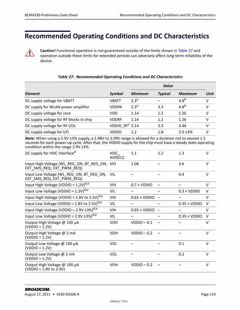
10/9/2011 7T5YL
Recommended Operating Conditions and DC Characteristics
BROADCOM August 17, 2011 • 4330-DS206-R Page 119
®
BCM4330 Preliminary Data Sheet
Recommended Operating Conditions and DC Characteristics
Caution! Functional operation is not guaranteed outside of the limits shown in Table 27 and operation outside these limits for extended periods can adversely affect long-term reliability of the device.
Table 27: Recommended Operating Conditions and DC Characteristics
Element Symbol
Value
UnitMinimum Typical Maximum
DC supply voltage for VBATT VBATT 2.3a – 4.8b V
DC supply for WLAN power amplifier VDDPA 2.3a 3.3 4.8b V
DC supply voltage for core VDD 1.14 1.2 1.26 V
DC supply voltage for RF blocks in chip VDDRF 1.14 1.2 1.26 V
DC supply voltage for RF I/Os VDDIO_RFc 3.14 3.3 3.46 V
DC supply voltage for I/O VDDIO 1.2 1.8 2.9 ±3% V
Note: When using a 2.9V ±3% supply, a 2.98V to 3.09V range is allowed for a duration not to exceed 1.5 seconds for each power-up cycle. After that, the VDDIO supply for the chip must have a steady state operating condition within the range 2.9V ±3%.
DC supply for HSIC interfaced HSIC_ AVDD12
1.1 1.2 1.3 V
Input High Voltage (WL_REG_ON, BT_REG_ON, EXT_SMS_REQ, EXT_PWM_REQ)
VIH 1.08 – 3.6 V
Input Low Voltage (WL_REG_ON, BT_REG_ON, EXT_SMS_REQ, EXT_PWM_REQ)
VIL – – 0.4 V
Input High Voltage (VDDIO = 1.2V)d,e VIH 0.7 × VDDIO – – V
Input Low Voltage (VDDIO = 1.2V)d,e VIL – – 0.3 × VDDIO V
Input High Voltage (VDDIO = 1.8V to 2.5V)d,e VIH 0.65 × VDDIO – – V
Input Low Voltage (VDDIO = 1.8V to 2.5V)d,e VIL – – 0.35 × VDDIO V
Input High Voltage (VDDIO = 2.9V ±3%)d,e VIH 0.65 × VDDIO – – V
Input Low Voltage (VDDIO = 2.9V ±3%)d,e VIL – – 0.35 × VDDIO V
Output High Voltage @ 100 µA (VDDIO = 1.2V)
VOH VDDIO – 0.1 – – V
Output High Voltage @ 2 mA (VDDIO = 1.2V)
VOH VDDIO – 0.2 – – V
Output Low Voltage @ 100 µA (VDDIO = 1.2V)
VOL – – 0.1 V
Output Low Voltage @ 2 mA (VDDIO = 1.2V)
VOL – – 0.2 V
Output High Voltage @ 100 µA (VDDIO = 1.8V to 2.9V)
VOH VDDIO – 0.2 – – V
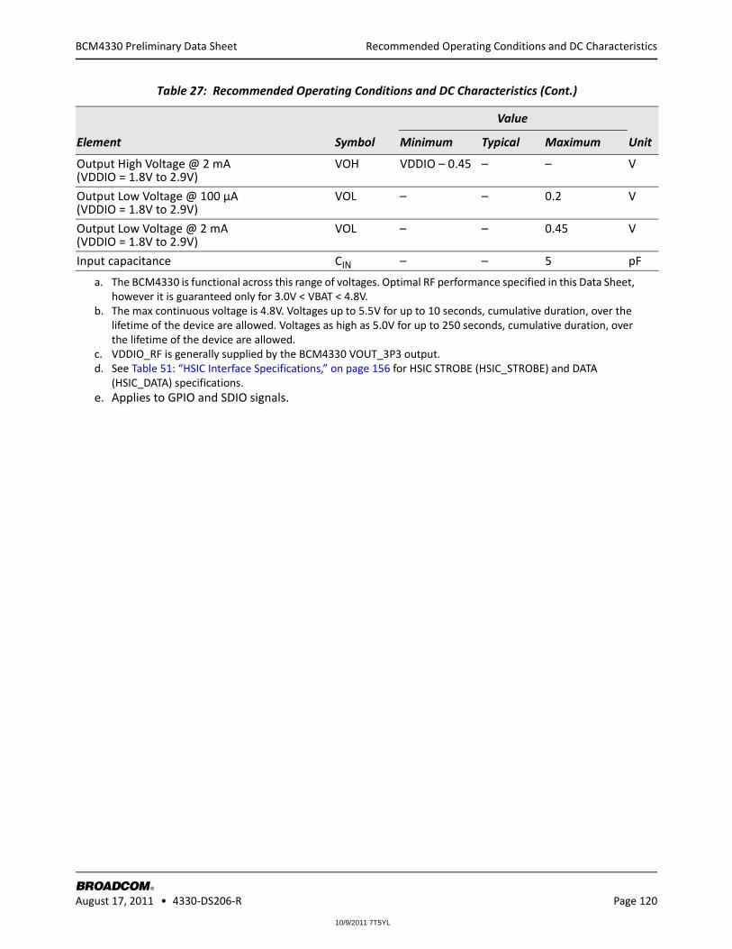
10/9/2011 7T5YL
Recommended Operating Conditions and DC Characteristics
BROADCOM August 17, 2011 • 4330-DS206-R Page 120
®
BCM4330 Preliminary Data Sheet
Output High Voltage @ 2 mA (VDDIO = 1.8V to 2.9V)
VOH VDDIO – 0.45 – – V
Output Low Voltage @ 100 µA (VDDIO = 1.8V to 2.9V)
VOL – – 0.2 V
Output Low Voltage @ 2 mA (VDDIO = 1.8V to 2.9V)
VOL – – 0.45 V
Input capacitance CIN – – 5 pF
a. The BCM4330 is functional across this range of voltages. Optimal RF performance specified in this Data Sheet, however it is guaranteed only for 3.0V < VBAT < 4.8V.
b. The max continuous voltage is 4.8V. Voltages up to 5.5V for up to 10 seconds, cumulative duration, over the lifetime of the device are allowed. Voltages as high as 5.0V for up to 250 seconds, cumulative duration, over the lifetime of the device are allowed.
c. VDDIO_RF is generally supplied by the BCM4330 VOUT_3P3 output.d. See Table 51: “HSIC Interface Specifications,” on page 156 for HSIC STROBE (HSIC_STROBE) and DATA
(HSIC_DATA) specifications.e. Applies to GPIO and SDIO signals.
Table 27: Recommended Operating Conditions and DC Characteristics (Cont.)
Element Symbol
Value
UnitMinimum Typical Maximum

10/9/2011 7T5YL
Bluetooth RF Specifications
BROADCOM August 17, 2011 • 4330-DS206-R Page 121
®
BCM4330 Preliminary Data Sheet
Section 16: Bluetooth RF Specifications
Unless otherwise stated, limit values apply for the conditions specified in Table 25: “Environmental Ratings,” on page 118 and Table 27: “Recommended Operating Conditions and DC Characteristics,” on page 119. Typical values apply for the following conditions:
• Vbatt = 3.6V
• Ambient temperature +25°C
Figure 41: RF Port Location for Bluetooth Testing
Note: Values in this data sheet are design goals and are subject to change based on the results of device characterization.
Note: All Bluetooth specifications are measured at the RF port unless otherwise specified.
Filter
BCM4330RF Switch
(0.5 dB Insertion Loss)
Antenna Port
RF Port
WLAN Tx
BT Tx
WLAN/BT Rx
ChipPort

10/9/2011 7T5YL
Bluetooth RF Specifications
BROADCOM August 17, 2011 • 4330-DS206-R Page 122
®
BCM4330 Preliminary Data Sheet
Table 28: Bluetooth Receiver RF Specifications
Parameter Conditions Minimum Typical Maximum Unit
General
Frequency range – 2402 – 2480 MHz
RX sensitivity GFSK, 0.1% BER, 1 Mbps – –93 – 87.5 dBm
π/4 – DQPSK, 0.01% BER, 2 Mbps
– –95 – 87.5 dBm
8 – DPSK, 0.01% BER, 3 Mbps
– –89 – 82.5 dBm
Input IP3 – –16 –9 – dBm
Maximum input at antenna – – – – 20 dBm
Return loss of BT Rx and Tx pins 50Ω port 10 – – dB
Interference Performance1
C/I cochannel GFSK, 0.1% BER – – 11.0 dB
C/I 1 MHz adjacent channel GFSK, 0.1% BER – – 0.0 dB
C/I 2 MHz adjacent channel GFSK, 0.1% BER – – –30.0 dB
C/I ≥ 3 MHz adjacent channel GFSK, 0.1% BER – – –40.0 dB
C/I image channel GFSK, 0.1% BER – – –9.0 dB
C/I 1 MHz adjacent to image channel
GFSK, 0.1% BER – – –20.0 dB
C/I cochannel π/4 – DQPSK, 0.1% BER – – 13.0 dB
C/I 1 MHz adjacent channel π/4 – DQPSK, 0.1% BER – – 0.0 dB
C/I 2 MHz adjacent channel π/4 – DQPSK, 0.1% BER – – –30.0 dB
C/I ≥ 3 MHz adjacent channel 8 – DPSK, 0.1% BER – – –40.0 dB
C/I image channel π/4 – DQPSK, 0.1% BER – – –7.0 dB
C/I 1 MHz adjacent to image channel
π/4 – DQPSK, 0.1% BER – – –20.0 dB
C/I cochannel 8 – DPSK, 0.1% BER – – 21.0 dB
C/I 1 MHz adjacent channel 8 – DPSK, 0.1% BER – – 5.0 dB
C/I 2 MHz adjacent channel 8 – DPSK, 0.1% BER – – –25.0 dB
C/I ≥ 3 MHz adjacent channel 8 – DPSK, 0.1% BER – – –33.0 dB
C/I Image channel 8 – DPSK, 0.1% BER – – 0.0 dB
C/I 1 MHz adjacent to image channel
8 – DPSK, 0.1% BER – – –13.0 dB
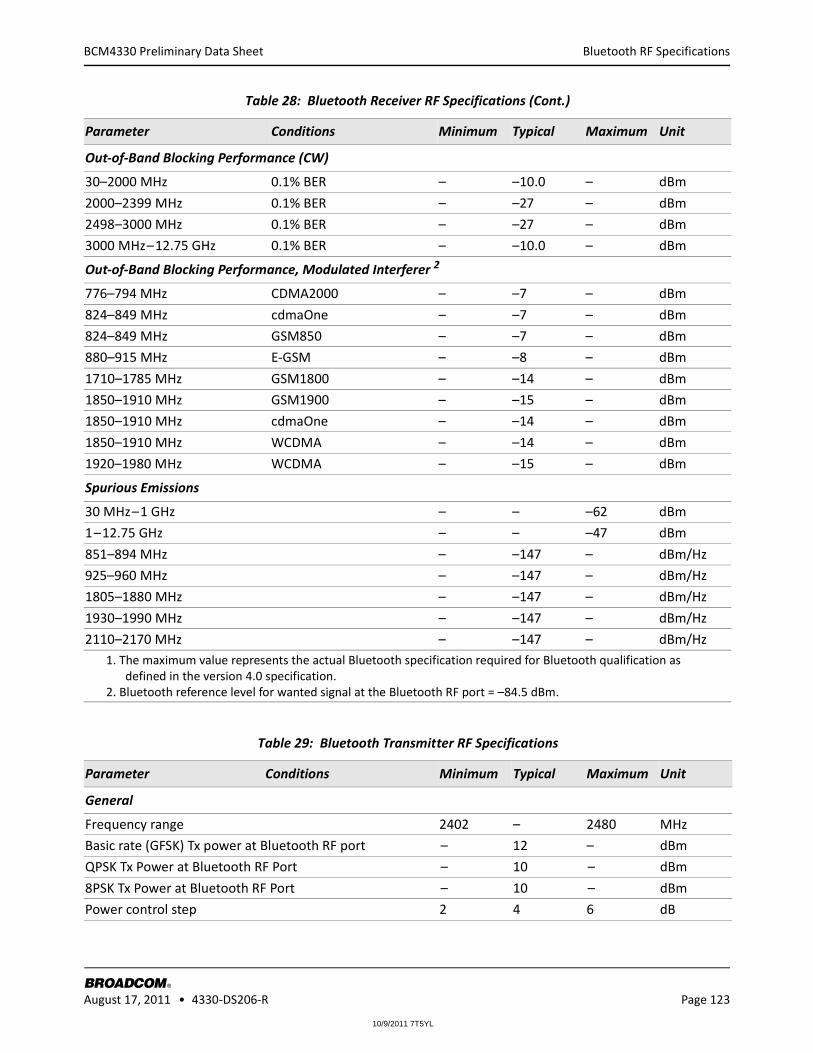
10/9/2011 7T5YL
Bluetooth RF Specifications
BROADCOM August 17, 2011 • 4330-DS206-R Page 123
®
BCM4330 Preliminary Data Sheet
Out-of-Band Blocking Performance (CW)
30–2000 MHz 0.1% BER – –10.0 – dBm
2000–2399 MHz 0.1% BER – –27 – dBm
2498–3000 MHz 0.1% BER – –27 – dBm
3000 MHz – 12.75 GHz 0.1% BER – –10.0 – dBm
Out-of-Band Blocking Performance, Modulated Interferer 2
776–794 MHz CDMA2000 – –7 – dBm
824–849 MHz cdmaOne – –7 – dBm
824–849 MHz GSM850 – –7 – dBm
880–915 MHz E-GSM – –8 – dBm
1710–1785 MHz GSM1800 – –14 – dBm
1850–1910 MHz GSM1900 – –15 – dBm
1850–1910 MHz cdmaOne – –14 – dBm
1850–1910 MHz WCDMA – –14 – dBm
1920–1980 MHz WCDMA – –15 – dBm
Spurious Emissions
30 MHz – 1 GHz – – –62 dBm
1 – 12.75 GHz – – –47 dBm
851–894 MHz – –147 – dBm/Hz
925–960 MHz – –147 – dBm/Hz
1805–1880 MHz – –147 – dBm/Hz
1930–1990 MHz – –147 – dBm/Hz
2110–2170 MHz – –147 – dBm/Hz1. The maximum value represents the actual Bluetooth specification required for Bluetooth qualification as
defined in the version 4.0 specification. 2. Bluetooth reference level for wanted signal at the Bluetooth RF port = –84.5 dBm.
Table 29: Bluetooth Transmitter RF Specifications
Parameter Conditions Minimum Typical Maximum Unit
General
Frequency range 2402 – 2480 MHz
Basic rate (GFSK) Tx power at Bluetooth RF port – 12 – dBm
QPSK Tx Power at Bluetooth RF Port – 10 – dBm
8PSK Tx Power at Bluetooth RF Port – 10 – dBm
Power control step 2 4 6 dB
Table 28: Bluetooth Receiver RF Specifications (Cont.)
Parameter Conditions Minimum Typical Maximum Unit
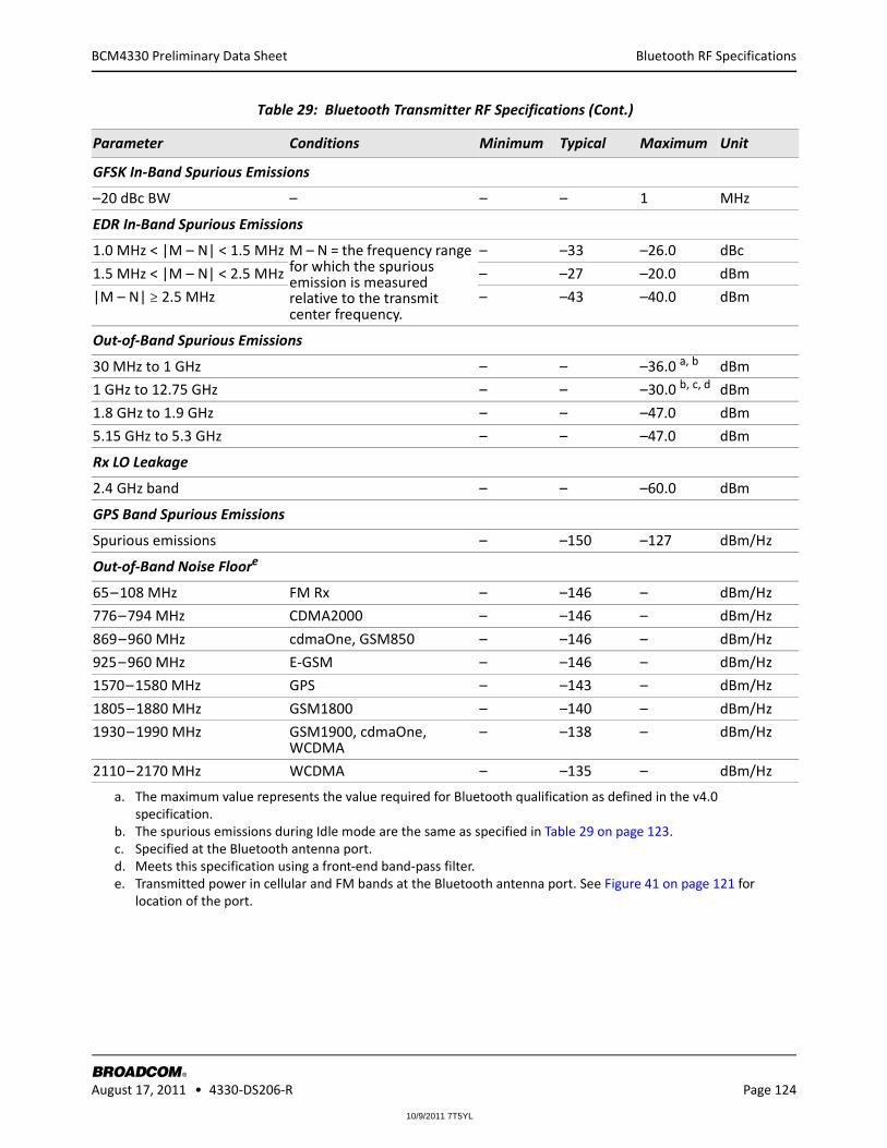
10/9/2011 7T5YL
Bluetooth RF Specifications
BROADCOM August 17, 2011 • 4330-DS206-R Page 124
®
BCM4330 Preliminary Data Sheet
GFSK In-Band Spurious Emissions
–20 dBc BW – – – 1 MHz
EDR In-Band Spurious Emissions
1.0 MHz < |M – N| < 1.5 MHz M – N = the frequency range for which the spurious emission is measured relative to the transmit center frequency.
– –33 –26.0 dBc
1.5 MHz < |M – N| < 2.5 MHz – –27 –20.0 dBm
|M – N| ≥ 2.5 MHz – –43 –40.0 dBm
Out-of-Band Spurious Emissions
30 MHz to 1 GHz – – –36.0 a, b dBm
1 GHz to 12.75 GHz – – –30.0 b, c, d dBm
1.8 GHz to 1.9 GHz – – –47.0 dBm
5.15 GHz to 5.3 GHz – – –47.0 dBm
Rx LO Leakage
2.4 GHz band – – –60.0 dBm
GPS Band Spurious Emissions
Spurious emissions – –150 –127 dBm/Hz
Out-of-Band Noise Floore
65 – 108 MHz FM Rx – –146 – dBm/Hz
776 – 794 MHz CDMA2000 – –146 – dBm/Hz
869 – 960 MHz cdmaOne, GSM850 – –146 – dBm/Hz
925 – 960 MHz E-GSM – –146 – dBm/Hz
1570 – 1580 MHz GPS – –143 – dBm/Hz
1805 – 1880 MHz GSM1800 – –140 – dBm/Hz
1930 – 1990 MHz GSM1900, cdmaOne, WCDMA
– –138 – dBm/Hz
2110 – 2170 MHz WCDMA – –135 – dBm/Hz
a. The maximum value represents the value required for Bluetooth qualification as defined in the v4.0 specification.
b. The spurious emissions during Idle mode are the same as specified in Table 29 on page 123.c. Specified at the Bluetooth antenna port.d. Meets this specification using a front-end band-pass filter.e. Transmitted power in cellular and FM bands at the Bluetooth antenna port. See Figure 41 on page 121 for
location of the port.
Table 29: Bluetooth Transmitter RF Specifications (Cont.)
Parameter Conditions Minimum Typical Maximum Unit
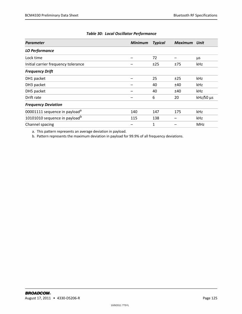
10/9/2011 7T5YL
Bluetooth RF Specifications
BROADCOM August 17, 2011 • 4330-DS206-R Page 125
®
BCM4330 Preliminary Data Sheet
Table 30: Local Oscillator Performance
Parameter Minimum Typical Maximum Unit
LO Performance
Lock time – 72 – µs
Initial carrier frequency tolerance – ±25 ±75 kHz
Frequency Drift
DH1 packet – 25 ±25 kHz
DH3 packet – 40 ±40 kHz
DH5 packet – 40 ±40 kHz
Drift rate – 6 20 kHz/50 µs
Frequency Deviation
00001111 sequence in payloada
a. This pattern represents an average deviation in payload.
140 147 175 kHz
10101010 sequence in payloadb
b. Pattern represents the maximum deviation in payload for 99.9% of all frequency deviations.
115 138 – kHz
Channel spacing – 1 – MHz
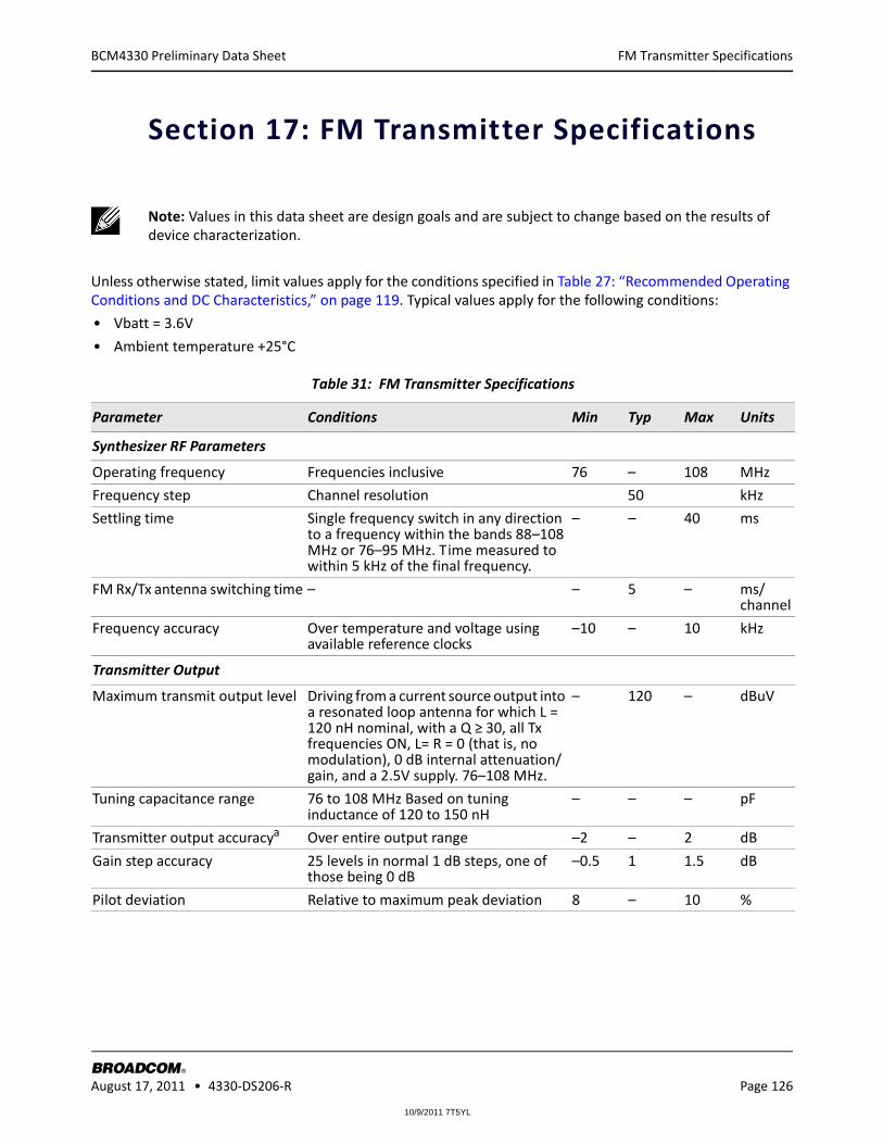
10/9/2011 7T5YL
FM Transmitter Specifications
BROADCOM August 17, 2011 • 4330-DS206-R Page 126
®
BCM4330 Preliminary Data Sheet
Section 17: FM Transmitter Specifications
Unless otherwise stated, limit values apply for the conditions specified in Table 27: “Recommended Operating Conditions and DC Characteristics,” on page 119. Typical values apply for the following conditions:
• Vbatt = 3.6V
• Ambient temperature +25°C
Note: Values in this data sheet are design goals and are subject to change based on the results of device characterization.
Table 31: FM Transmitter Specifications
Parameter Conditions Min Typ Max Units
Synthesizer RF Parameters
Operating frequency Frequencies inclusive 76 – 108 MHz
Frequency step Channel resolution 50 kHz
Settling time Single frequency switch in any direction to a frequency within the bands 88–108 MHz or 76–95 MHz. Time measured to within 5 kHz of the final frequency.
– – 40 ms
FM Rx/Tx antenna switching time – – 5 – ms/channel
Frequency accuracy Over temperature and voltage using available reference clocks
–10 – 10 kHz
Transmitter Output
Maximum transmit output level Driving from a current source output into a resonated loop antenna for which L = 120 nH nominal, with a Q ≥ 30, all Tx frequencies ON, L= R = 0 (that is, no modulation), 0 dB internal attenuation/gain, and a 2.5V supply. 76–108 MHz.
– 120 – dBuV
Tuning capacitance range 76 to 108 MHz Based on tuning inductance of 120 to 150 nH
– – – pF
Transmitter output accuracya Over entire output range –2 – 2 dB
Gain step accuracy 25 levels in normal 1 dB steps, one of those being 0 dB
–0.5 1 1.5 dB
Pilot deviation Relative to maximum peak deviation 8 – 10 %

10/9/2011 7T5YL
FM Transmitter Specifications
BROADCOM August 17, 2011 • 4330-DS206-R Page 127
®
BCM4330 Preliminary Data Sheet
Transmitted spectrum for maximum deviation
Total peak deviation set to 75 kHz. Audio tone of 1 kHz, pilot = 6.75 kHz.
– – – –
0 kHz offset from carrier – – 0 dBc
± 50 kHz offset – – 0 dBc
± 75 kHz offset – – 0 dBc
± 120 kHz offset – – –12.2 dBc
Occupied BW ± 100 kHz offset from nominal channel freq
– – –20 dBc
Transmitter noise floor From 850 MHz to 2.4 GHz – – – dBm/Hz
Composite transmitted deviation L = R set to 75 mV rms, stereo enabled – – ± 75 kHz peak
Transmitter spurious Load 120 nH: Q 30 – – – –
746–764 MHz – – 19 dBuV
869–894 MHz, 925–960 MHz, 1805–1880 MHz, 1930–1990 MHz
– – 12 dBuV
2110–2170 MHz – – 20 dBuV
1570–1580 MHz – – 6 dBuV
Transmitted deviation flatness Change in audio level for 75 kHz deviation over 76–108 MHz
– – ±1 dB
Channel balance 1 kHz tone for 22.5 kHz audio deviation L = R, pilot 6.75 kHz
–1 – 1 dB
Stereo separation 1 kHz tone for 22.5 kHz audio deviation L ≠ R, pilot 6.75 kHz
27 40 dB
Lower 3 dB pointb (measured with receiver set to correct de-emphasis)
– – 50 Hz
Upper 3 dB pointa 15 – – kHz
Pre-emphasis time constant High – 75 – µs
Low – 50 – µs
Tolerance – – ± 5 %
Distortion 75 kHz total deviation including 6.75 kHz pilot, 1 kHz modulation rate
– 0.1 1 %
Transmitted S/N depends on the 32.768 kHz sleep clock phase noise performance
Deviation set to 22.5 kHz with 6.75 kHz pilot deviation. Measured with 50 µS de-emphasis and A-weighted filter. Forced Mono
– 60 – dB
As above in Stereo – 56 – dB
Audio spurious products Δf = 22.5 kHz, fmod = 1 kHz, de-emphasis = 50 µs, L = R, BAF = 300 Hz to 15 kHz, fTX = 76 to 108 MHz
– – –60 dBcb
a. Relative to mean power in the band.b. With respect to a 1 kHz tone.
Table 31: FM Transmitter Specifications (Cont.)
Parameter Conditions Min Typ Max Units
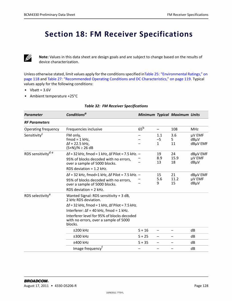
10/9/2011 7T5YL
FM Receiver Specifications
BROADCOM August 17, 2011 • 4330-DS206-R Page 128
®
BCM4330 Preliminary Data Sheet
Section 18: FM Receiver Specifications
Unless otherwise stated, limit values apply for the conditions specified inTable 25: “Environmental Ratings,” on page 118 and Table 27: “Recommended Operating Conditions and DC Characteristics,” on page 119. Typical values apply for the following conditions:
• Vbatt = 3.6V
• Ambient temperature +25°C
Note: Values in this data sheet are design goals and are subject to change based on the results of device characterization.
Table 32: FM Receiver Specifications
Parameter Conditionsa Minimum Typical Maximum Units
RF Parameters
Operating frequency Frequencies inclusive 65b – 108 MHz
Sensitivityc FM only, fmod = 1 kHz, Δf = 22.5 kHz, (S+N)/N ≥ 26 dB
– – –
1.1 –5 1
3.6 5 11
µV EMF dBµV dBµV EMF
RDS sensitivityd e Δf = 32 kHz, fmod = 1 kHz, Δf Pilot = 7.5 kHz.95% of blocks decoded with no errors, over a sample of 5000 blocks.RDS deviation = 1.2 kHz.
– – –
19 8.9 13
24 15.9 18
dBµV EMF µV EMF dBµV
Δf = 32 kHz, fmod=1 kHz, Δf Pilot = 7.5 kHz.95% of blocks decoded with no errors, over a sample of 5000 blocks.RDS deviation = 2 kHz.
– – –
15 5.6 9
21 11.2 15
dBµV EMF µV EMF dBµV
RDS selectivitye Wanted Signal: RDS sensitivity + 3 dB, 2 kHz RDS deviation.Δf = 32 kHz, fmod = 1 kHz, Δf Pilot = 7.5 kHz.Interferer: Δf = 40 kHz, fmod = 1 kHz.Interferer level for 95% of blocks decoded with no errors, over a sample of 5000 blocks.
±200 kHz S + 16 – – dB
±300 kHz S + 25 – – dB
±400 kHz S + 35 – – dB
Image frequencyf – – – dB

10/9/2011 7T5YL
FM Receiver Specifications
BROADCOM August 17, 2011 • 4330-DS206-R Page 129
®
BCM4330 Preliminary Data Sheet
Receiver adjacent channel selectivityg
Measured for 40 dB SNR at the audio output. Wanted Signal: 23 dBµV EMF (14.1 µV EMF) Δf = 75 kHz, fmod = 1 kHz, Δf pilot = 7.5 kHz. Interferer: Δf = 40 kHz, fmod = 1 kHz. At ±200 kHz.
S + 16 – – dB
At ±300 kHz and above S + 25 – – dB
Image response, mono At fWanted ±2fIF, depending on LO injection side relative to fWanted. Measured for 40 dB SNR at the audio output. Wanted signal: 66 dBµV EMF (2 mV EMF), Δf = 75 kHz, fmod = 1 kHz. Interferer: Δf = 40 kHz, fmod = 1 kHz.
25 – – dB
In-band blocking At fWanted ±1 MHz to fWanted + 400 kHz in 100 kHz steps. Measured for 40 dB SNR at the audio output. Wanted signal: 23 dBµV EMF (14.1 µV EMF), Δf = 75 kHz, fmod = 1 kHz. Interferer: Δf = 40 kHz, fmod = 1 kHz.
S + 35 – – dB
AM suppression, monoc Vin = 23 dBµV EMF (14.1 µV EMF), Δf = 22.5 kHz, fmod = 1 kHz. AM at 400 Hz with m = 0.3. No A-weighted or any other filtering applied.
40 – – dB
Intermediate signal plus noise-to-noise ratio (S+N)/N, stereoc
Vin = 20 dBµV EMF (10 µV EMF), Δf = 22.5 kHz, fmod = 1 kHz. BAF = 300 Hz to 15 kHz, A-weighted mono.
45 – – dB
Intermodulation performancec
Vin = 20 dBµV EMF (10 µV EMF), Δf = 22.5 kHz, fmod = 1 kHz. BAF = 300 Hz to 15 kHz, A-weighted mono.
S + 32 – – dB
RF Input
RF input impedance – 1.5 – – kΩ
RF input levelc Δf = 22.5 kHz, fmod = 1 kHz. SNR > 26 dB.
– – 111 dBµV EMF
– – 354 mV EMF
– – 105 dBµV
RF conducted emissions Local oscillator breakthrough measured on the reference port
– – –55 dBm
925–960 MHz, 1805 –1880 MHz, and 1930–1990 MHz
– – –90 dBm
Table 32: FM Receiver Specifications (Cont.)
Parameter Conditionsa Minimum Typical Maximum Units

10/9/2011 7T5YL
FM Receiver Specifications
BROADCOM August 17, 2011 • 4330-DS206-R Page 130
®
BCM4330 Preliminary Data Sheet
RF blocking levels at the FM antenna input 26 dB SNR. (Assumes presence of an external matching circuit.)
824–915 MHz, GSM 200 kHz BW, CDMA 1.2 MHz BW
0 – – dBm
1710–1980 MHz, GSM 200 kHz BW, CDMA 1.2 MHz BW, WCDMA 4 MHz BW
–5 – – dBm
Tuning
Frequency step – 10 – – kHz
Settling time Single frequency switch in any direction to a frequency within the bands 88–108 MHz or 76–90 MHz. Time measured to within 5 kHz of the final frequency.
– 150 – µs
Sweep time Total time for an automatic search to sweep from 88–108 MHz or 76–90 MHz (and reverse direction) assuming no channels found.
– – 8 sec
General Audio
Audio output levelh Vin = 66 dBµV EMF (2 mV EMF), Δf = 22.5 kHz, fmod = 1 kHz, Δf pilot = 6.75 kHz.
– 14 60
– 75
– 12.5 90
dBFS mV rms
Maximum audio output leveli
Vin = 66 dBµV EMF(2 mV EMF), Δf = 100 kHz, fmod = 1 kHz, Δf pilot = 6.75 kHz.
– –
– –
0 333
dBFS mV rms
Audio output level differencej
Vin = 66 dBµV EMF (2 mV EMF), Δf = 22.5 kHz, fmod = 1 kHz.
–1 – –1 dB
Left and right AC mute FM input signal fully muted with DAC enabled.
60 – – dB
Left and right hard mute FM input signal fully muted with DAC disabled.
80 – – dB
Soft mute attenuation and start level
Muting is performed dynamically proportional to the FM wanted input signal C/N. The muting characteristic is fully programmable. See Section 9: “FM Transceiver Subsystem,” on page 64 for more information.
– – – –
Maximum signal plus noise-to-noise ratio (S+N)/N, monoj
Vin = 66 dBµV EMF(2 mV EMF), Δf = 22.5 kHz, fmod = 1 kHz.
– 60 – dB
Maximum signal plus noise-to-noise ratio (S+N)/N, stereoj
– 56 – dB
Table 32: FM Receiver Specifications (Cont.)
Parameter Conditionsa Minimum Typical Maximum Units

10/9/2011 7T5YL
FM Receiver Specifications
BROADCOM August 17, 2011 • 4330-DS206-R Page 131
®
BCM4330 Preliminary Data Sheet
Total harmonic distortion, mono
Vin = 66 dBµV EMF (2 mV EMF), Δf = 75 kHz, fmod = 400 Hz.
– – 0.8 %
Vin = 66 dBµV EMF (2 mV EMF), Δf = 75 kHz, fmod = 1 kHz.
– – 0.8 %
Vin = 66 dBµV EMF (2 mV EMF), Δf = 75 kHz, fmod = 3 kHz.
– – 0.8 %
Vin = 66 dBµV EMF (2 mV EMF), Δf = 100 kHz, fmod = 1 kHz.
– – 1.0 %
Total harmonic distortion, stereo
Vin = 66 dBµV EMF (2 mV EMF), Δf = 67.5 kHz, fmod = 1 kHz, Δf Pilot = 6.75 kHz, L=R.
– – 1.5 %
Audio spurious productsj
Vin = 66 dBµV EMF (2 mV EMF), Δf = 22.5 kHz, fmod = 1 kHz, Range from 300 Hz to 15 kHz, with respect to 1 kHz tone.
– – –60 dBc
Audio bandwidth, upper (–3 dB point)
Vin = 66 dBµV EMF (2 mV EMF), Δf = 8 kHz, for 50 µs.
15 – – kHz
Audio bandwidth, lower (–3 dB point)
– – 20 Hz
Audio in-band ripple 100 Hz to 13 kHz, Vin = 66 dBµV EMF (2 mV EMF), Δf = 8 kHz, for 50 µs.
–0.5 – 0.5 dB
Deemphasis time constant tolerance
With respect to 50 and 75 µs – – ±5 %
RSSI range With 1 dB resolution and ±3 dB accuracy at room temperature
3 1.41 –3
– – –
83 14100 77
dBµV EMF µV EMF dBµV
Pause Detection
Audio level at which a pause is detected
Relative to a 1-kHz tone, 22.5 kHz deviation
– – – –
4 values in 3 dB steps –21 – –12 dB
Audio pause duration 4 values 20 – 40 ms
Table 32: FM Receiver Specifications (Cont.)
Parameter Conditionsa Minimum Typical Maximum Units

10/9/2011 7T5YL
FM Receiver Specifications
BROADCOM August 17, 2011 • 4330-DS206-R Page 132
®
BCM4330 Preliminary Data Sheet
Figure 42: FM Receiver Circuit
Stereo Decoder
Stereo channel separation
Forced Stereo mode. Vin = 66 dBµV EMF (2 mV EMF), Δf = 67.5 kHz, fmod = 1 kHz, Δf Pilot = 6.75 kHz, R = 0, L = 1.
– 40 – dB
Mono/stereo blend and switching
Blending and switching is dynamically proportional to the FM wanted input signal C/N. The blending and switching characteristics are fully programmable. See Section 9: “FM Transceiver Subsystem,” on page 64 for more information.
– – – –
Pilot suppression Vin = 66 dBµV EMF (2 mV EMF), Δf = 75 kHz, fmod = 1 kHz.
46 – – dB
a. The following conditions apply to all relevant tests unless otherwise indicated: Preemphasis and deemphasis of 50 µs, R = L for mono, DAC Load > 20 kΩ, BAF = 300 Hz to 15 kHz, A-weighted filtering.
b. Contact Broadcom regarding applications that will operate between 65 and 76 MHz.c. Wanted signal: Δf = 22.5 kHz, fmod = 1 kHz.d. RDS sensitivity numbers are for 87.5 to 108 MHz only.e. Vin = Δf = 32 kHz, fmod = 1 kHz, Δf pilot = 7.5 kHz, 95% of blocks decoded with no errors over a sample of 5000
blocks.f. The best tune algorithm is used during normal operation to avoid image interference.g. Wanted Signal: Δf = 22.5 kHz, fmod = 1 kHz, Δf pilot = 7.5 kHz.h. Vin = 66 dBµV EMF (2 mV EMF), Δf = 22.5 kHz, fmod = 1 kHz, Δf pilot = 6.75 kHz.i. Vin = 66 dBµV EMF (2 mV EMF), Δf = 100 kHz, fmod = 1 kHz, Δf pilot = 6.75 kHz.j. Vin = 66 dBµV EMF (2 mV EMF), Δf = 22.5 kHz, fmod = 1 kHz.
Table 32: FM Receiver Specifications (Cont.)
Parameter Conditionsa Minimum Typical Maximum Units

10/9/2011 7T5YL
WLAN RF Specifications
BROADCOM August 17, 2011 • 4330-DS206-R Page 133
®
BCM4330 Preliminary Data Sheet
Section 19: WLAN RF Specifications
Introduction The BCM4330 includes an integrated dual-band direct conversion radio that supports either the 2.4 GHz band or the 5 GHz band. The BCM4330 does not provide simultaneous 2.4 GHz and 5 GHz operation. This section describes the RF characteristics of the 2.4 GHz and 5 GHz portions of the radio.
Unless otherwise stated, limit values apply for the conditions specified inTable 25: “Environmental Ratings,” on page 118 and Table 27: “Recommended Operating Conditions and DC Characteristics,” on page 119. Typical values apply for the following conditions:
• Vbatt = 3.6V
• Ambient temperature +25°C
Figure 43: Port Locations
Note: Values in this data sheet are design goals and are subject to change based on the results of device characterization.
Note: All WLAN specifications are measured at the chip port, unless otherwise specified.
Filter
BCM4330RF Switch
(0.5 dB Insertion Loss)
Antenna Port
RF Port
WLAN Tx
BT Tx
WLAN/BT Rx
ChipPort

10/9/2011 7T5YL
2.4 GHz Band General RF Specifications
BROADCOM August 17, 2011 • 4330-DS206-R Page 134
®
BCM4330 Preliminary Data Sheet
2.4 GHz Band General RF Specifications
WLAN 2.4 GHz Receiver Performance Specifications
Table 33: 2.4 GHz Band General RF Specifications
Item Condition Minimum Typical Maximum Unit
Tx/Rx switch time Including TX ramp down – – 5 µs
Rx/Tx switch time Including TX ramp up – – 2 µs
Power-up and power-down ramp time
DSSS/CCK modulations – – < 2 µs
Note: The specifications in Table 34 are measured at the chip port, unless otherwise specified.
Table 34: WLAN 2.4 GHz Receiver Performance Specifications
Parameter Condition/Notes Minimum Typical Maximum Unit
Frequency range – 2400 – 2500 MHz
RX sensitivity(8% PER for 1024 octet PSDU)a
1 Mbps DSSS – 96.5 –98 – dBm
2 Mbps DSSS – 92 –94 – dBm
5.5 Mbps DSSS – 90.5 –92 – dBm
11 Mbps DSSS – 88 –90 – dBm
RX sensitivity(10% PER for 1000 octet PSDU)a
6 Mbps OFDM – 89 –92 – dBm
9 Mbps OFDM – –90.5 – dBm
12 Mbps OFDM – 86 –89 – dBm
18 Mbps OFDM – –88 – dBm
24 Mbps OFDM – 84 –86 – dBm
36 Mbps OFDM – –83 – dBm
48 Mbps OFDM – –78 – dBm
54 Mbps OFDM – 75 –77 – dBm

10/9/2011 7T5YL
WLAN 2.4 GHz Receiver Performance Specifications
BROADCOM August 17, 2011 • 4330-DS206-R Page 135
®
BCM4330 Preliminary Data Sheet
RX sensitivity(10% PER for 4096 octet PSDU)a,b. Defined for default parameters: GF, 800 ns GI, and non-STBC.
20 MHz channel spacing for all MCS rates
MCS 7 – 71.5 –74 – dBm
MCS 6 – –74.5 – dBm
MCS 5 – –76.5 – dBm
MCS 4 – 79 –80.5 – dBm
MCS 3 – –84 – dBm
MCS 2 – –86.5 – dBm
MCS 1 – –88.5 – dBm
MCS0 – 88 –92 – dBm
Blocking level for 1dB Rx sensitivity degradation (without external filtering)c
776–794 MHz CDMA2000 – – 24 – dBm
824–849 MHzd cdmaOne – – 25 – dBm
824–849 MHz GSM850 – – 15 – dBm
880–915 MHz E-GSM – – 16 – dBm
1710–1785 MHz GSM1800 – – 18 – dBm
1850–1910 MHz GSM1800 – – 19 – dBm
1850–1910 MHz cdmaOne – – 26 – dBm
1850–1910 MHz WCDMA – – 26 – dBm
1920–1980 MHz WCDMA – – 28.5 – dBm
2500-2690 MHz WiMAX – – 45 – dBm
In-band static CW jammer immunity(fc – 8 MHz < fcw + 8 MHz)
Rx PER < 1%, 54 MbpsOFDM, 1000 octet PSDU for: (RxSens + 23 dB < Rxlevel < max input level)
–80 – – dBm
Input In-Band IP3a Maximum LNA gain – –15.5 – dBm
Minimum LNA gain – –1.5 – dBm
Maximum Receive Level@ 2.4 GHz
@ 1, 2 Mbps (8% PER, 1024 octets) –3.5 – – dBm
@ 5.5, 11 Mbps (8% PER, 1024 octets) –9.5 – – dBm
@ 6–54 Mbps (10% PER, 1024 octets) –9.5 – – dBm
@ MCS0–7 rates (10% PER, 4095 octets) –9.5 – – dBm
LPF 3 dB Bandwidth – 9 – 10 MHz
Adjacent channel rejection-DSSS(Difference between interfering and desired signal at 8% PER for 1024 octet PSDU with desired signal level as specified in Condition/Notes)
Desired and interfering signal 30 MHz apart
1 Mbps DSSS –74 dBm 35 – – dB
2 Mbps DSSS –74 dBm 35 – – dB
Desired and interfering signal 25 MHz apart
5.5 Mbps DSSS –70 dBm 35 – – dB
11 Mbps DSSS –70 dBm 35 – – dB
Table 34: WLAN 2.4 GHz Receiver Performance Specifications (Cont.)
Parameter Condition/Notes Minimum Typical Maximum Unit
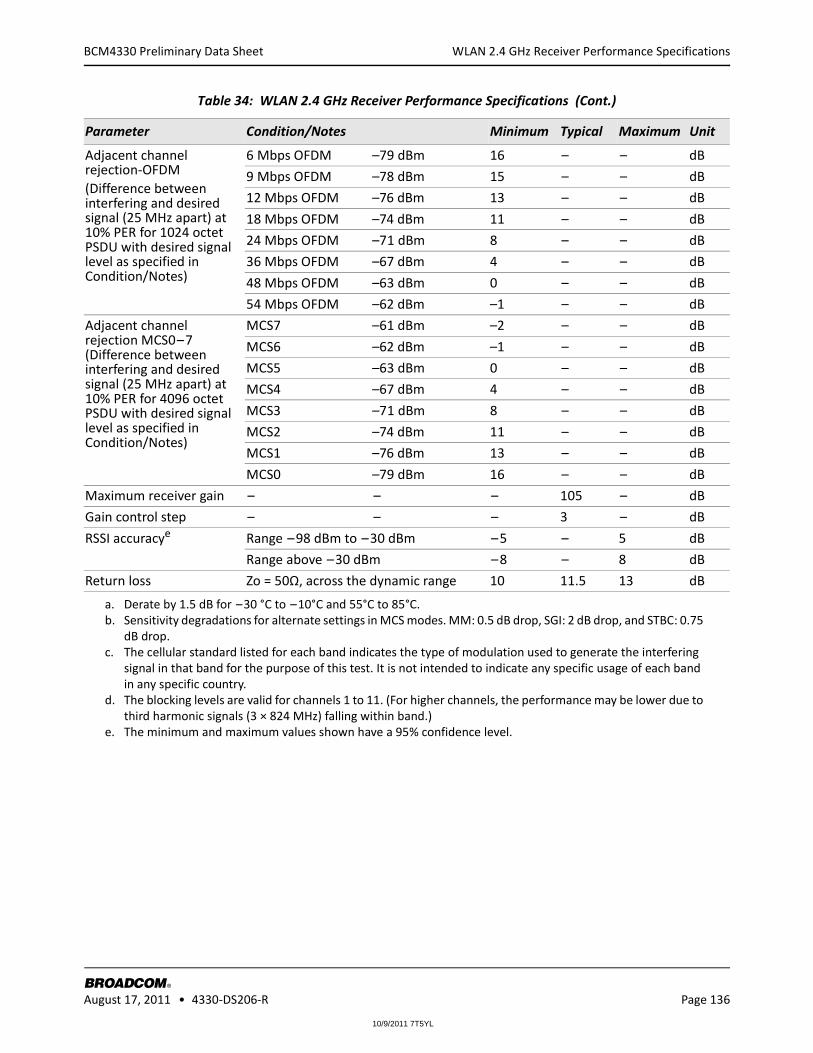
10/9/2011 7T5YL
WLAN 2.4 GHz Receiver Performance Specifications
BROADCOM August 17, 2011 • 4330-DS206-R Page 136
®
BCM4330 Preliminary Data Sheet
Adjacent channel rejection-OFDM(Difference between interfering and desired signal (25 MHz apart) at 10% PER for 1024 octet PSDU with desired signal level as specified in Condition/Notes)
6 Mbps OFDM –79 dBm 16 – – dB
9 Mbps OFDM –78 dBm 15 – – dB
12 Mbps OFDM –76 dBm 13 – – dB
18 Mbps OFDM –74 dBm 11 – – dB
24 Mbps OFDM –71 dBm 8 – – dB
36 Mbps OFDM –67 dBm 4 – – dB
48 Mbps OFDM –63 dBm 0 – – dB
54 Mbps OFDM –62 dBm –1 – – dB
Adjacent channel rejection MCS0 – 7 (Difference between interfering and desired signal (25 MHz apart) at 10% PER for 4096 octet PSDU with desired signal level as specified in Condition/Notes)
MCS7 –61 dBm –2 – – dB
MCS6 –62 dBm –1 – – dB
MCS5 –63 dBm 0 – – dB
MCS4 –67 dBm 4 – – dB
MCS3 –71 dBm 8 – – dB
MCS2 –74 dBm 11 – – dB
MCS1 –76 dBm 13 – – dB
MCS0 –79 dBm 16 – – dB
Maximum receiver gain – – – 105 – dB
Gain control step – – – 3 – dB
RSSI accuracye Range – 98 dBm to – 30 dBm – 5 – 5 dB
Range above – 30 dBm – 8 – 8 dB
Return loss Zo = 50Ω, across the dynamic range 10 11.5 13 dB
a. Derate by 1.5 dB for – 30 °C to – 10°C and 55°C to 85°C.b. Sensitivity degradations for alternate settings in MCS modes. MM: 0.5 dB drop, SGI: 2 dB drop, and STBC: 0.75
dB drop.c. The cellular standard listed for each band indicates the type of modulation used to generate the interfering
signal in that band for the purpose of this test. It is not intended to indicate any specific usage of each band in any specific country.
d. The blocking levels are valid for channels 1 to 11. (For higher channels, the performance may be lower due to third harmonic signals (3 × 824 MHz) falling within band.)
e. The minimum and maximum values shown have a 95% confidence level.
Table 34: WLAN 2.4 GHz Receiver Performance Specifications (Cont.)
Parameter Condition/Notes Minimum Typical Maximum Unit

10/9/2011 7T5YL
WLAN 2.4 GHz Transmitter Performance Specifications
BROADCOM August 17, 2011 • 4330-DS206-R Page 137
®
BCM4330 Preliminary Data Sheet
WLAN 2.4 GHz Transmitter Performance Specifications
Note: The specifications in Table 35 are measured at the chip port output, unless otherwise specified.
Table 35: WLAN 2.4 GHz Transmitter Performance Specifications
Parameter Condition/Notes Minimum Typical Maximum Unit
Frequency range – 2400 – 2500 MHz
Transmitted power in cellular and FM bands (at 21 dBm, >90% duty cycle, 1 Mbps CCK)a
76 – 108 MHz FM Rx – –149 – dBm/Hz
776 – 794 MHz – – –127 – dBm/Hz
869 – 960 MHz cdmaOne, GSM850
– –163 – dBm/Hz
925 – 960 MHz E-GSM – –163 – dBm/Hz
1570 – 1580 MHz GPS – –150 – dBm/Hz
1805 – 1880 MHz GSM1800 – –141 – dBm/Hz
1930 – 1990 MHz GSM1900, cdmaOne, WCDMA
– –138 – dBm/Hz
2110 – 2170 MHz WCDMA – –129 – dBm/Hz
2.5 to 3.6 GHz WIMAX CH1 – – 115 to – 142
– dBm/Hz
2.5 to 3.6 GHz WIMAX CH13 – – 113 to – 145
– dBm/Hz
Harmonic level (at 18 dBm with 100% duty cycle)
4.8 – 5.0 GHz 2nd harmonic – – –10 dBm/1 MHz
7.2 – 7.5 GHz 3rd harmonic – – –28 dBm/1 MHz
EVM Does Not Exceed
Tx power for highest power level setting at 25°C, VBATT = 3.6V and spectral mask and EVM complianceb, c
802.11b (DSSS/CCK)
–9 dB 19 20.5 – dBm
OFDM, BPSK –8 dB 19 20 – dBm
OFDM, QPSK –13 dB 19 20 – dBm
OFDM, 16-QAM –19 dB 17.5 19 – dBm
OFDM, 64-QAM (R = 3/4)
–25 dB 16.5 18 – dBm
OFDM, 64-QAM (R = 5/6)
–28 dB 15.5 17 – dBm
Tx power control dynamic range
– 10 – – dB
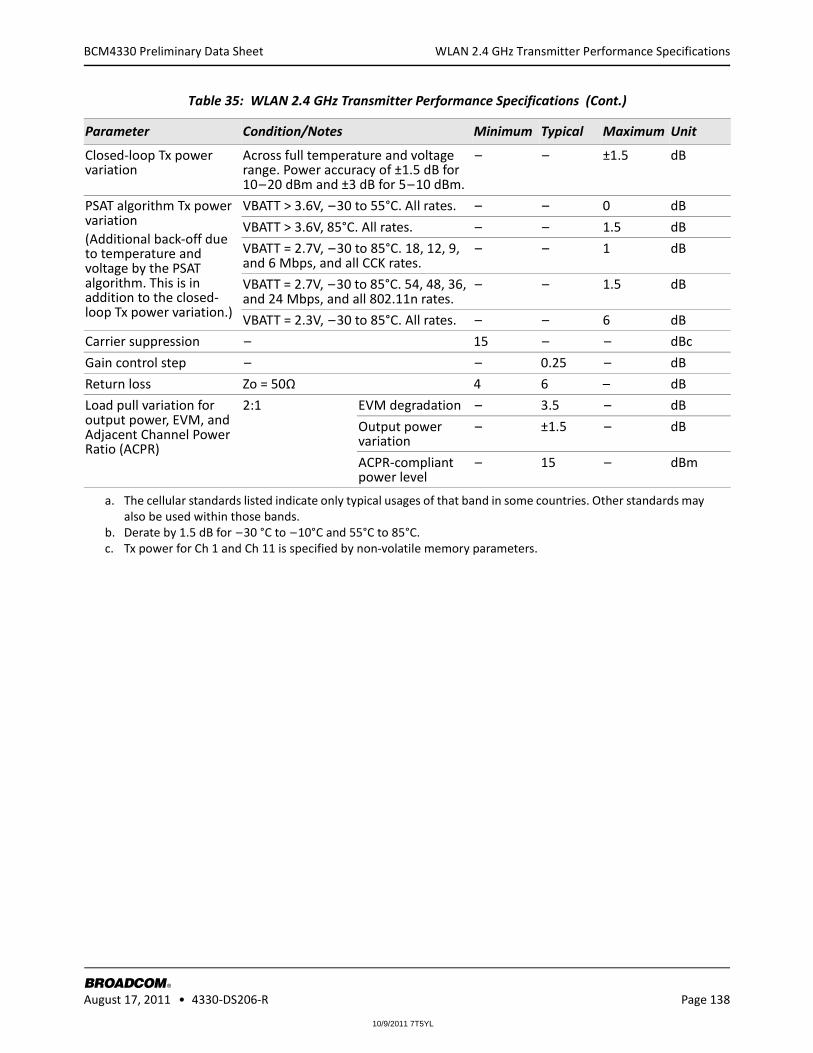
10/9/2011 7T5YL
WLAN 2.4 GHz Transmitter Performance Specifications
BROADCOM August 17, 2011 • 4330-DS206-R Page 138
®
BCM4330 Preliminary Data Sheet
Closed-loop Tx power variation
Across full temperature and voltage range. Power accuracy of ±1.5 dB for 10 – 20 dBm and ±3 dB for 5 – 10 dBm.
– – ±1.5 dB
PSAT algorithm Tx power variation(Additional back-off due to temperature and voltage by the PSAT algorithm. This is in addition to the closed-loop Tx power variation.)
VBATT > 3.6V, – 30 to 55°C. All rates. – – 0 dB
VBATT > 3.6V, 85°C. All rates. – – 1.5 dB
VBATT = 2.7V, – 30 to 85°C. 18, 12, 9, and 6 Mbps, and all CCK rates.
– – 1 dB
VBATT = 2.7V, – 30 to 85°C. 54, 48, 36, and 24 Mbps, and all 802.11n rates.
– – 1.5 dB
VBATT = 2.3V, – 30 to 85°C. All rates. – – 6 dB
Carrier suppression – 15 – – dBc
Gain control step – – 0.25 – dB
Return loss Zo = 50Ω 4 6 – dB
Load pull variation for output power, EVM, and Adjacent Channel Power Ratio (ACPR)
2:1 EVM degradation – 3.5 – dB
Output power variation
– ±1.5 – dB
ACPR-compliant power level
– 15 – dBm
a. The cellular standards listed indicate only typical usages of that band in some countries. Other standards may also be used within those bands.
b. Derate by 1.5 dB for – 30 °C to – 10°C and 55°C to 85°C.c. Tx power for Ch 1 and Ch 11 is specified by non-volatile memory parameters.
Table 35: WLAN 2.4 GHz Transmitter Performance Specifications (Cont.)
Parameter Condition/Notes Minimum Typical Maximum Unit

10/9/2011 7T5YL
WLAN 5 GHz Receiver Performance Specifications
BROADCOM August 17, 2011 • 4330-DS206-R Page 139
®
BCM4330 Preliminary Data Sheet
WLAN 5 GHz Receiver Performance Specifications
Note: The specifications in Table 36 are measured at the chip port input, unless otherwise specified.
Table 36: WLAN 5 GHz Receiver Performance Specifications
Parameter Condition/Notes Minimum Typical Maximum Unit
Frequency range – 4900 – 5845 MHz
RX sensitivity(10% PER for 1000 octet PSDU)a
6 Mbps OFDM – – 86.5 – dBm
9 Mbps OFDM – – 85 – dBm
12 Mbps OFDM – – 84 – dBm
18 Mbps OFDM – – 82 – dBm
24 Mbps OFDM – – 81 – dBm
36 Mbps OFDM – – 78 – dBm
48 Mbps OFDM – – 74 – dBm
54 Mbps OFDM – – 71 – dBm
RX sensitivity(10% PER for 4096 octet PSDU)a
HT mode MCS 7 (64 QAM, R = 5/6, 20 MHz channel spacing)
– – 68 – dBm
Blocking level for 1 dB Rx sensitivity degradation (without external filtering)b
776–794 MHz CDMA2000 – – 19.5 – dBm
824–849 MHz cdmaOne – – 21.5 – dBm
824–849 MHz GSM850 – – 10 – dBm
880–915 MHz E-GSM – – 9.5 – dBm
1710–1785 MHz GSM1800 – – 13.5 – dBm
1850–1910 MHz GSM1800 – – 13.5 – dBm
1850–1910 MHz cdmaOne – – 20.5 – dBm
1850–1910 MHz WCDMA – – 20.5 – dBm
1920–1980 MHz WCDMA – – 20.5 – dBm
2500-2690 MHz WiMAX – –21 – dBm
Input in-band IP3a Maximum LNA gain – –15.5 – dBm
Minimum LNA gain – –1.5 – dBm
Maximum receive level@ 5.24 GHz
@ 6, 9, 12 Mbps –9.5 – – dBm
@ 18, 24, 36, 48, 54 Mbps –14.5 – – dBm
LPF 3 dB bandwidth – 9 – 10 MHz
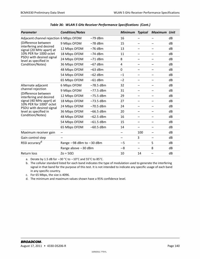
10/9/2011 7T5YL
WLAN 5 GHz Receiver Performance Specifications
BROADCOM August 17, 2011 • 4330-DS206-R Page 140
®
BCM4330 Preliminary Data Sheet
Adjacent channel rejection(Difference between interfering and desired signal (20 MHz apart) at 10% PER for 1000 octet PSDU with desired signal level as specified in Condition/Notes)
6 Mbps OFDM –79 dBm 16 – – dB
9 Mbps OFDM –78 dBm 15 – – dB
12 Mbps OFDM –76 dBm 13 – – dB
18 Mbps OFDM –74 dBm 11 – – dB
24 Mbps OFDM –71 dBm 8 – – dB
36 Mbps OFDM –67 dBm 4 – – dB
48 Mbps OFDM –63 dBm 0 – – dB
54 Mbps OFDM –62 dBm –1 – – dB
65 Mbps OFDM –61 dBm –2 – – dB
Alternate adjacent channel rejection(Difference between interfering and desired signal (40 MHz apart) at 10% PER for 1000c octet PSDU with desired signal level as specified in Condition/Notes)
6 Mbps OFDM –78.5 dBm 32 – – dB
9 Mbps OFDM –77.5 dBm 31 – – dB
12 Mbps OFDM –75.5 dBm 29 – – dB
18 Mbps OFDM –73.5 dBm 27 – – dB
24 Mbps OFDM –70.5 dBm 24 – – dB
36 Mbps OFDM –66.5 dBm 20 – – dB
48 Mbps OFDM –62.5 dBm 16 – – dB
54 Mbps OFDM –61.5 dBm 15 – – dB
65 Mbps OFDM –60.5 dBm 14 – – dB
Maximum receiver gain – – 100 – dB
Gain control step – – 3 – dB
RSSI accuracyd Range – 98 dBm to – 30 dBm – 5 – 5 dB
Range above – 30 dBm – 8 – 8 dB
Return loss Zo = 50Ω 10 14 – dB
a. Derate by 1.5 dB for – 30 °C to – 10°C and 55°C to 85°C.b. The cellular standard listed for each band indicates the type of modulation used to generate the interfering
signal in that band for the purpose of this test. It is not intended to indicate any specific usage of each band in any specific country.
c. For 65 Mbps, the size is 4096.d. The minimum and maximum values shown have a 95% confidence level.
Table 36: WLAN 5 GHz Receiver Performance Specifications (Cont.)
Parameter Condition/Notes Minimum Typical Maximum Unit

10/9/2011 7T5YL
WLAN 5 GHz Transmitter Performance Specifications
BROADCOM August 17, 2011 • 4330-DS206-R Page 141
®
BCM4330 Preliminary Data Sheet
WLAN 5 GHz Transmitter Performance Specifications
Note: The specifications in Table 37 are measured at the chip port, unless otherwise specified.
Table 37: WLAN 5 GHz Transmitter Performance Specifications
Parameter Condition/Notes Minimum Typical Maximum Unit
Frequency range – 4900 – 5845 MHz
Transmitted power in cellular and FM bands (at 18 dBm)a
76 – 108 MHz FM Rx – – 162 – dBm/Hz
776 – 794 MHz – – – 162 – dBm/Hz
869 – 960 MHz cdmaOne, GSM850
– – 162 – dBm/Hz
925 – 960 MHz E-GSM – – 162 – dBm/Hz
1570 – 1580 MHz GPS – – 162 – dBm/Hz
1805 – 1880 MHz GSM1800 – – 162 – dBm/Hz
1930 – 1990 MHz GSM1900, cdmaOne, WCDMA
– – 162 – dBm/Hz
2110 – 2170 MHz WCDMA – – 162 – dBm/Hz
2400 – 2483 MHz BT/WLAN – – 162 – dBm/Hz
Harmonic level (at 17 dBm)
9.8–11.570 GHz 2nd harmonic – – 31 – dBm/MHz
EVM Does Not Exceed
Tx power for highest power level setting at 25°C, VBATT = 3.6V and spectral mask and EVM complianceb
OFDM, BPSK –8 dB – 16 – dBm
OFDM, 64-QAM (R = 3/4)
–25 dB – 15 – dBm
OFDM, 64-QAM (R = 5/6)
–28 dB – 13 – dBm
Tx power control dynamic range
– 10 – – dB
Tx power control resolution
– 0.5 – – dB
Closed loop Tx power variation at highest power level setting
Across full temperature and voltage range
– – ±2 dB
Carrier suppression – 15 – – dBc
Gain control step – – 0.25 – dB
Return loss Zo = 50Ω – 6 – dB
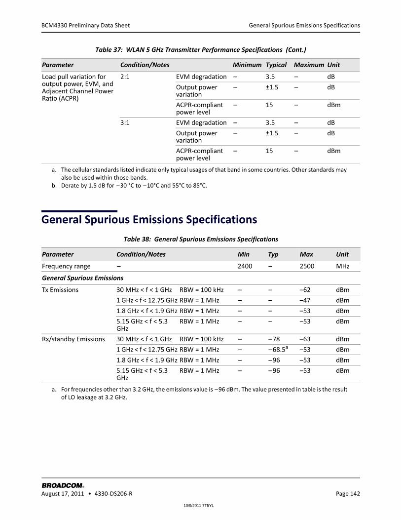
10/9/2011 7T5YL
General Spurious Emissions Specifications
BROADCOM August 17, 2011 • 4330-DS206-R Page 142
®
BCM4330 Preliminary Data Sheet
General Spurious Emissions Specifications
Load pull variation for output power, EVM, and Adjacent Channel Power Ratio (ACPR)
2:1 EVM degradation – 3.5 – dB
Output power variation
– ±1.5 – dB
ACPR-compliant power level
– 15 – dBm
3:1 EVM degradation – 3.5 – dB
Output power variation
– ±1.5 – dB
ACPR-compliant power level
– 15 – dBm
a. The cellular standards listed indicate only typical usages of that band in some countries. Other standards may also be used within those bands.
b. Derate by 1.5 dB for – 30 °C to – 10°C and 55°C to 85°C.
Table 38: General Spurious Emissions Specifications
Parameter Condition/Notes Min Typ Max Unit
Frequency range – 2400 – 2500 MHz
General Spurious Emissions
Tx Emissions 30 MHz < f < 1 GHz RBW = 100 kHz – – –62 dBm
1 GHz < f < 12.75 GHz RBW = 1 MHz – – –47 dBm
1.8 GHz < f < 1.9 GHz RBW = 1 MHz – – –53 dBm
5.15 GHz < f < 5.3 GHz
RBW = 1 MHz – – –53 dBm
Rx/standby Emissions 30 MHz < f < 1 GHz RBW = 100 kHz – – 78 –63 dBm
1 GHz < f < 12.75 GHz RBW = 1 MHz – – 68.5a
a. For frequencies other than 3.2 GHz, the emissions value is – 96 dBm. The value presented in table is the result of LO leakage at 3.2 GHz.
–53 dBm
1.8 GHz < f < 1.9 GHz RBW = 1 MHz – – 96 –53 dBm
5.15 GHz < f < 5.3 GHz
RBW = 1 MHz – – 96 –53 dBm
Table 37: WLAN 5 GHz Transmitter Performance Specifications (Cont.)
Parameter Condition/Notes Minimum Typical Maximum Unit
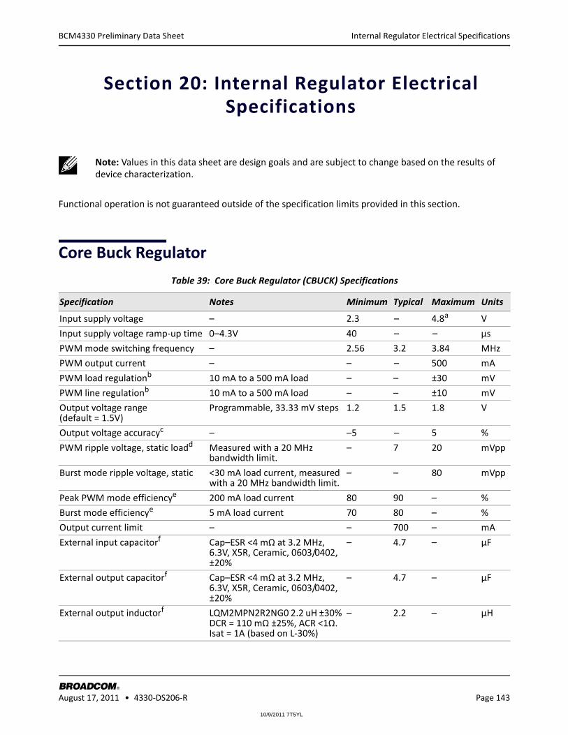
10/9/2011 7T5YL
Internal Regulator Electrical Specifications
BROADCOM August 17, 2011 • 4330-DS206-R Page 143
®
BCM4330 Preliminary Data Sheet
Section 20: Internal Regulator Electrical Specifications
Functional operation is not guaranteed outside of the specification limits provided in this section.
Core Buck Regulator
Note: Values in this data sheet are design goals and are subject to change based on the results of device characterization.
Table 39: Core Buck Regulator (CBUCK) Specifications
Specification Notes Minimum Typical Maximum Units
Input supply voltage – 2.3 – 4.8a V
Input supply voltage ramp-up time 0–4.3V 40 – – µs
PWM mode switching frequency – 2.56 3.2 3.84 MHz
PWM output current – – – 500 mA
PWM load regulationb 10 mA to a 500 mA load – – ±30 mV
PWM line regulationb 10 mA to a 500 mA load – – ±10 mV
Output voltage range (default = 1.5V)
Programmable, 33.33 mV steps 1.2 1.5 1.8 V
Output voltage accuracyc – –5 – 5 %
PWM ripple voltage, static loadd Measured with a 20 MHz bandwidth limit.
– 7 20 mVpp
Burst mode ripple voltage, static <30 mA load current, measured with a 20 MHz bandwidth limit.
– – 80 mVpp
Peak PWM mode efficiencye 200 mA load current 80 90 – %
Burst mode efficiencye 5 mA load current 70 80 – %
Output current limit – – 700 – mA
External input capacitorf Cap–ESR <4 mΩ at 3.2 MHz, 6.3V, X5R, Ceramic, 0603/0402, ±20%
– 4.7 – µF
External output capacitorf Cap–ESR <4 mΩ at 3.2 MHz, 6.3V, X5R, Ceramic, 0603/0402, ±20%
– 4.7 – µF
External output inductorf LQM2MPN2R2NG0 2.2 uH ±30% DCR = 110 mΩ ±25%, ACR <1Ω. Isat = 1A (based on L-30%)
– 2.2 – µH

10/9/2011 7T5YL
LDO3p1
BROADCOM August 17, 2011 • 4330-DS206-R Page 144
®
BCM4330 Preliminary Data Sheet
LDO3p1
Start-up time from power downg – – – 1400 µs
a. The max continuous voltage is 4.8V. Voltages up to 5.5V for up to 10 seconds, cumulative duration, over the lifetime of the device are allowed. Voltages as high as 5.0V for up to 250 seconds, cumulative duration, over the lifetime of the device are allowed.
b. VBAT = 2.7 to 4.8V, inductor DCR <137.5 mΩc. Includes line/load regulation, VBAT = 2.7 to 4.8V, load 0 to 500 mA, inductor DCR <137.5 mΩd. Max ripple based on VBAT <4.3V, Vout = 1.5V, Fs = 3.2 MHz, 1.5 uH inductor L >1.05 uH, cap + board total–ESR
<10 mΩ, Cout > 1.9 µFe. VBAT<4.3V, inductor DCR <137.5 mΩ, ACR <1Ωf. Critical CBuck component – see Reference [1] on page 19 for details and required characteristics of external
PMU components.g. Start-up time is measured with respect to the rising edge of BT_REG_ON, WL_REG_ON, or EXT_SMPS_REQ.
Table 40: LDO3p1 Specifications
Specification Notes Minimum Typical Maximum Units
Input supply voltage – 2.3 3.6 4.8a
a. The max continuous voltage is 4.8V. Voltages up to 5.5V for up to 10 seconds, cumulative duration, over the lifetime of the device are allowed. Voltages as high as 5.0V for up to 250 seconds, cumulative duration, over the lifetime of the device are allowed.
V
Output current – – – 80 mA
Output voltage range (default = 3.1V)
Programmable, 100 mV steps
2.4 3.1 3.4 V
Output voltage accuracyb
b. VBAT = 3.3 to 4.8V for 3.1V VOUT.
Includes line/load regulation
–5 – 5 %
Drop-out voltage At maximum load – – 200 mV
Quiescent current No load – 8 – µA
External output capacitor cd
c. See Reference [1] on page 19 for details and required characteristics of external PMU components.d. Ceramic, X5R, 0402, ESR 30~200 mΩ, ±10%, 10V.
– – 2.2 – µF
External input capacitorc SR_VDDBAT2 pin, ceramic, X5R, 0402, ESR 30–200 mΩ, ±10%, 10V
– 1 – µF
Start-up time from power down – – – 1400 µs
LDO turn-on time Chip already powered up – – 100 µs
Table 39: Core Buck Regulator (CBUCK) Specifications
Specification Notes Minimum Typical Maximum Units

10/9/2011 7T5YL
LDO3p3
BROADCOM August 17, 2011 • 4330-DS206-R Page 145
®
BCM4330 Preliminary Data Sheet
LDO3p3
Table 41: LDO3p3 Specifications
Specification Notes Minimum Typical Maximum Units
Input supply voltage – 2.3 3.6 4.8a
a. The max continuous voltage is 4.8V. Voltages up to 5.5V for up to 10 seconds, cumulative duration, over the lifetime of the device are allowed. Voltages as high as 5.0V for up to 250 seconds, cumulative duration, over the lifetime of the device are allowed.
V
Output current – – – 80 mA
Output voltage range (default = 3.3V)
Programmable, 100 mV steps 2.4 3.3 3.4 V
Output voltage accuracyb
b. VBAT = 3.5 to 4.8V for 3.3V VOUT.
Includes line/load regulation –5 – 5 %
Drop-out voltage At maximum load – – 200 mV
Quiescent current No load – 8 – µA
External output capacitorcd
c. ESR: 30–200 mΩd. See Reference [1] on page 19 for details and required characteristics of external PMU components.
– – 4.7 – µF
External input capacitord SR_VDDBAT2 pin, ceramic, X5R, 0402, ESR 30–200 mΩ, ±10%, 10V
– 1 – µF
Start-up time from power-down – – 500 1000 µs
LDO turn-on time Chip already powered up – – 100 µs
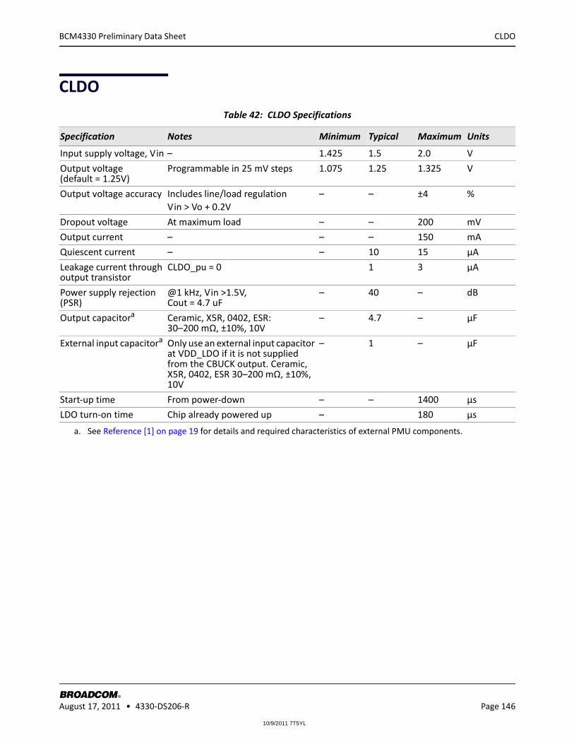
10/9/2011 7T5YL
CLDO
BROADCOM August 17, 2011 • 4330-DS206-R Page 146
®
BCM4330 Preliminary Data Sheet
CLDO
Table 42: CLDO Specifications
Specification Notes Minimum Typical Maximum Units
Input supply voltage, Vin – 1.425 1.5 2.0 V
Output voltage (default = 1.25V)
Programmable in 25 mV steps 1.075 1.25 1.325 V
Output voltage accuracy Includes line/load regulationVin > Vo + 0.2V
– – ±4 %
Dropout voltage At maximum load – – 200 mV
Output current – – – 150 mA
Quiescent current – – 10 15 µA
Leakage current through output transistor
CLDO_pu = 0 1 3 µA
Power supply rejection (PSR)
@1 kHz, Vin >1.5V, Cout = 4.7 uF
– 40 – dB
Output capacitora
a. See Reference [1] on page 19 for details and required characteristics of external PMU components.
Ceramic, X5R, 0402, ESR: 30–200 mΩ, ±10%, 10V
– 4.7 – µF
External input capacitora Only use an external input capacitor at VDD_LDO if it is not supplied from the CBUCK output. Ceramic, X5R, 0402, ESR 30–200 mΩ, ±10%, 10V
– 1 – µF
Start-up time From power-down – – 1400 µs
LDO turn-on time Chip already powered up – 180 µs

10/9/2011 7T5YL
LNLDO1
BROADCOM August 17, 2011 • 4330-DS206-R Page 147
®
BCM4330 Preliminary Data Sheet
LNLDO1
Table 43: LNLDO1 Specificationsa
a. See Reference [1] on page 19 for details and required characteristics of external PMU components.
Specification Notes Minimum Typical Maximum Units
Input Supply Voltage – 1.425 1.5 2.0 V
Output Voltage (default = 1.25V)
Programmable in 25 mV steps 1.10 1.25 1.35 V
Output Voltage Accuracyb
b. Include line/load regulation, Vin >Vo + 0.2V
– – – ± 4 %
Output Current – – – 300 mA
Dropout Voltage (at max load)
– – – 200 mV
Quiescent Current – 62 88 µA
Leakage Current – – 0.1 10 µA
Output Noise @ 30 kHz, 60 mA load – – 60 nV/rt Hz
PSR @ 1 kHz, Vin >1.5V, Cout = 4.7 µF – 50 – dB
External Output Capacitor
Ceramic, X5R, 0402, ESR 30–200 mΩ, ±10%, 10V
– 4.7 – µF
Start-up time – – – 1400 µs
LDO Turn-on Time Chip already powered up – – 180 µs
10/9/2011 7T5YL
System Power Consumption
BROADCOM August 17, 2011 • 4330-DS206-R Page 148
®
BCM4330 Preliminary Data Sheet
Section 21: System Power Consumption
Note: Values in this data sheet are design goals and are subject to change based on the results of device characterization. Unless otherwise stated, these values apply for the conditions specified in Table 27: “Recommended Operating Conditions and DC Characteristics,” on page 119.
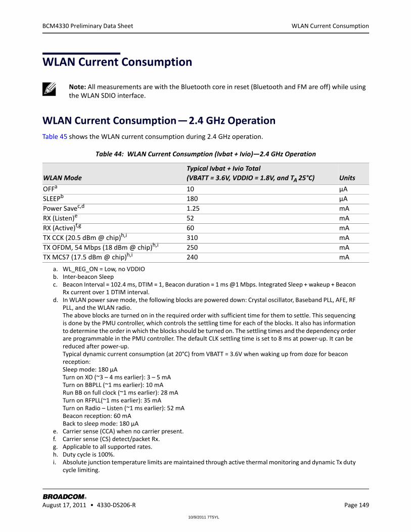
10/9/2011 7T5YL
WLAN Current Consumption
BROADCOM August 17, 2011 • 4330-DS206-R Page 149
®
BCM4330 Preliminary Data Sheet
WLAN Current Consumption
WLAN Current Consumption — 2.4 GHz OperationTable 45 shows the WLAN current consumption during 2.4 GHz operation.
Note: All measurements are with the Bluetooth core in reset (Bluetooth and FM are off) while using the WLAN SDIO interface.
Table 44: WLAN Current Consumption (Ivbat + Ivio)—2.4 GHz Operation
WLAN ModeTypical Ivbat + Ivio Total(VBATT = 3.6V, VDDIO = 1.8V, and TA 25°C) Units
OFFa
a. WL_REG_ON = Low, no VDDIO
10 µASLEEPb
b. Inter-beacon Sleep
180 µAPower Savec,d
c. Beacon Interval = 102.4 ms, DTIM = 1, Beacon duration = 1 ms @1 Mbps. Integrated Sleep + wakeup + Beacon Rx current over 1 DTIM interval.
d. In WLAN power save mode, the following blocks are powered down: Crystal oscillator, Baseband PLL, AFE, RF PLL, and the WLAN radio.The above blocks are turned on in the required order with sufficient time for them to settle. This sequencing is done by the PMU controller, which controls the settling time for each of the blocks. It also has information to determine the order in which the blocks should be turned on. The settling times and the dependency order are programmable in the PMU controller. The default CLK settling time is set to 8 ms at power-up. It can be reduced after power-up.Typical dynamic current consumption (at 20°C) from VBATT = 3.6V when waking up from doze for beacon reception:Sleep mode: 180 µATurn on XO (~3 – 4 ms earlier): 3 – 5 mATurn on BBPLL (~1 ms earlier): 10 mARun BB on full clock (~1 ms earlier): 28 mATurn on RFPLL(~1 ms earlier): 35 mATurn on Radio – Listen (~1 ms earlier): 52 mABeacon reception: 60 mABack to sleep mode: 180 µA
1.25 mARX (Listen)e
e. Carrier sense (CCA) when no carrier present.
52 mARX (Active)f,g
f. Carrier sense (CS) detect/packet Rx.g. Applicable to all supported rates.
60 mATX CCK (20.5 dBm @ chip)h,i
h. Duty cycle is 100%.i. Absolute junction temperature limits are maintained through active thermal monitoring and dynamic Tx duty
cycle limiting.
310 mATX OFDM, 54 Mbps (18 dBm @ chip)h,i 250 mATX MCS7 (17.5 dBm @ chip)h,i 240 mA
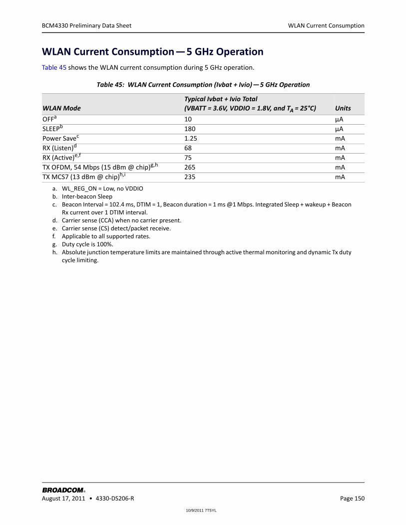
10/9/2011 7T5YL
WLAN Current Consumption
BROADCOM August 17, 2011 • 4330-DS206-R Page 150
®
BCM4330 Preliminary Data Sheet
WLAN Current Consumption — 5 GHz OperationTable 45 shows the WLAN current consumption during 5 GHz operation.
Table 45: WLAN Current Consumption (Ivbat + Ivio) — 5 GHz Operation
WLAN ModeTypical Ivbat + Ivio Total(VBATT = 3.6V, VDDIO = 1.8V, and TA = 25°C) Units
OFFa
a. WL_REG_ON = Low, no VDDIO
10 µASLEEPb
b. Inter-beacon Sleep
180 µAPower Savec
c. Beacon Interval = 102.4 ms, DTIM = 1, Beacon duration = 1 ms @1 Mbps. Integrated Sleep + wakeup + Beacon Rx current over 1 DTIM interval.
1.25 mARX (Listen)d
d. Carrier sense (CCA) when no carrier present.
68 mARX (Active)e,f
e. Carrier sense (CS) detect/packet receive.f. Applicable to all supported rates.
75 mATX OFDM, 54 Mbps (15 dBm @ chip)g,h
g. Duty cycle is 100%.h. Absolute junction temperature limits are maintained through active thermal monitoring and dynamic Tx duty
cycle limiting.
265 mATX MCS7 (13 dBm @ chip)h,i 235 mA

10/9/2011 7T5YL
HSIC Interface Current Consumption
BROADCOM August 17, 2011 • 4330-DS206-R Page 151
®
BCM4330 Preliminary Data Sheet
HSIC Interface Current ConsumptionThe HSIC interface current consumption measurements are shown in Table 46.
Bluetooth and FM Current ConsumptionThe Bluetooth and FM current consumption measurements are shown in Table 47.
Table 46: HSIC Interface Current Consumption
State Typical Current in mA (AVDD+DVDD @ 1.2V)
Standby 0.012Active, Idle 10.12Active, Worst case pattern 18.22
Note: The WLAN core is in reset (WLAN_RST_N = low) for all measurements provided in Table 47.
Note: For FM measurements, the Bluetooth core is in sleep mode. The current consumption numbers are measured based on the typical output power as specified in Table 29 on page 123.
Table 47: Bluetooth and FM Current Consumption
Operating ModeVBATT (VBATT = 3.6V) Typical
VDDIO (VDDIO = 1.8V) Typical Units
Sleep 0.14 0.15 mAStandard 1.28s Inquiry Scan 0.34 – mA3DH5/3DH1 Master 24.8 – mA3DH5/3DH1 Slave 24.8 – mAHV3 + Sniff + Scana
a. At maximum class 1 TX power, 500 ms sniff, four attempts (slave), P = 1.28s, and I = 2.56s.
14.2 – mAP & I Scanb
b. 1.28s page/inquiry scan interval.
529 5 µA500 ms Sniff Master 0.24 – mA500 ms Sniff Slave 0.24 – mADM1/DH1 Master 32 – mADM3/DH3 Master 40 – mADM5/DH5 Master 41 – mAFMRX I2S Audio 14.7 – mAFMRX Analog Audio 15.3 – mA

10/9/2011 7T5YL
Interface Timing and AC Characteristics
BROADCOM August 17, 2011 • 4330-DS206-R Page 152
®
BCM4330 Preliminary Data Sheet
Section 22: Interface T iming and AC Characteristics
SDIO/gSPI Timing
SDIO Default Mode Timing SDIO default mode timing is shown by the combination of Figure 44 and Table 48 on page 153.
Figure 44: SDIO Bus Timing (Default Mode)
tWL tWH
fPP
tTHL
tISU
tTLH
tIH
tODLY(max)
tODLY(min)
Input
Output
SDIO_CLK
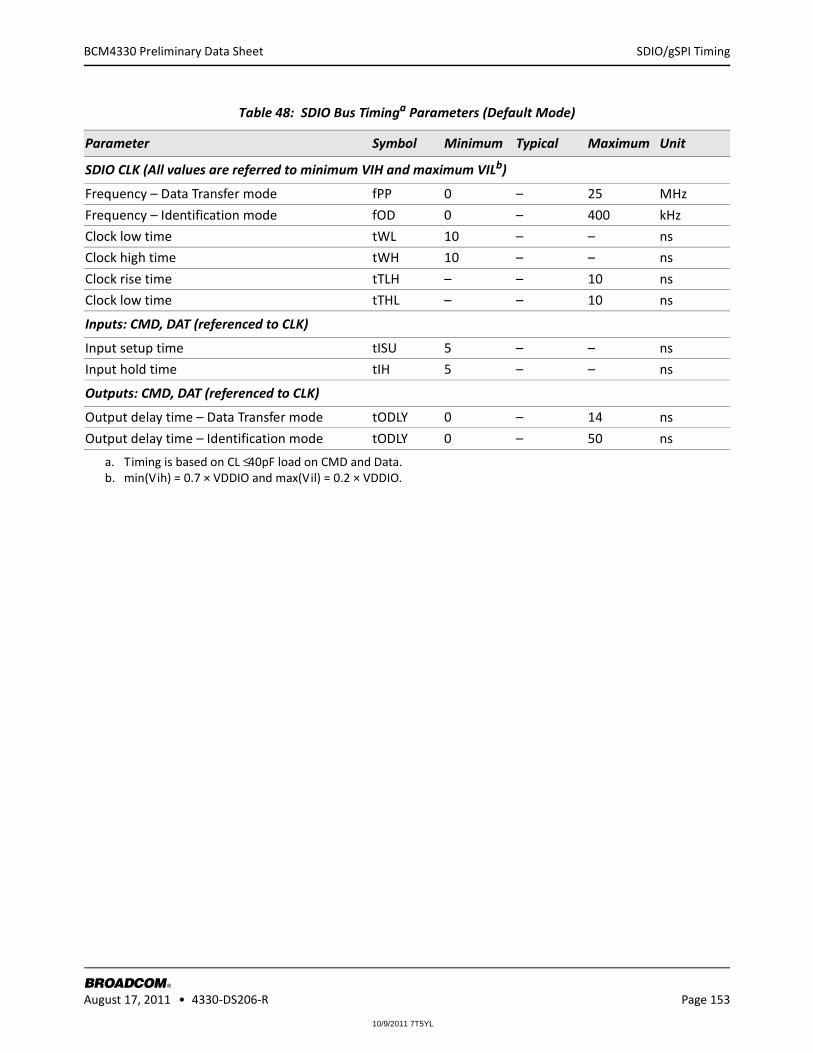
10/9/2011 7T5YL
SDIO/gSPI Timing
BROADCOM August 17, 2011 • 4330-DS206-R Page 153
®
BCM4330 Preliminary Data Sheet
Table 48: SDIO Bus Timinga Parameters (Default Mode)
a. Timing is based on CL ≤ 40pF load on CMD and Data.
Parameter Symbol Minimum Typical Maximum Unit
SDIO CLK (All values are referred to minimum VIH and maximum VILb)
b. min(Vih) = 0.7 × VDDIO and max(Vil) = 0.2 × VDDIO.
Frequency – Data Transfer mode fPP 0 – 25 MHz
Frequency – Identification mode fOD 0 – 400 kHz
Clock low time tWL 10 – – ns
Clock high time tWH 10 – – ns
Clock rise time tTLH – – 10 ns
Clock low time tTHL – – 10 ns
Inputs: CMD, DAT (referenced to CLK)
Input setup time tISU 5 – – ns
Input hold time tIH 5 – – ns
Outputs: CMD, DAT (referenced to CLK)
Output delay time – Data Transfer mode tODLY 0 – 14 ns
Output delay time – Identification mode tODLY 0 – 50 ns

10/9/2011 7T5YL
SDIO/gSPI Timing
BROADCOM August 17, 2011 • 4330-DS206-R Page 154
®
BCM4330 Preliminary Data Sheet
SDIO High-Speed Mode TimingSDIO high-speed mode timing is shown by the combination of Figure 45 and Table 49.
Figure 45: SDIO Bus Timing (High-Speed Mode)
Table 49: SDIO Bus Timinga Parameters (High-Speed Mode)
a. Timing is based on CL ≤ 40pF load on CMD and Data.
Parameter Symbol Minimum Typical Maximum Unit
SDIO CLK (all values are referred to minimum VIH and maximum VILb)
b. min(Vih) = 0.7 × VDDIO and max(Vil) = 0.2 × VDDIO.
Frequency – Data Transfer Mode fPP 0 – 50 MHz
Frequency – Identification Mode fOD 0 – 400 kHz
Clock low time tWL 7 – – ns
Clock high time tWH 7 – – ns
Clock rise time tTLH – – 3 ns
Clock low time tTHL – – 3 ns
Inputs: CMD, DAT (referenced to CLK)
Input setup Time tISU 6 – – ns
Input hold Time tIH 2 – – ns
Outputs: CMD, DAT (referenced to CLK)
Output delay time – Data Transfer Mode tODLY – – 14 ns
Output hold time tOH 2.5 – – ns
Total system capacitance (each line) CL – – 40 pF
tWL tWH
fPP
tTHL
tISU
tTLH
tIH
tODLY
Input
Output
50% VDD
tOH
SDIO_CLK

10/9/2011 7T5YL
SDIO/gSPI Timing
BROADCOM August 17, 2011 • 4330-DS206-R Page 155
®
BCM4330 Preliminary Data Sheet
gSPI Signal TimingThe gSPI host and device always use the rising edge of clock to sample data.
Figure 46: gSPI Timing
Table 50: gSPI Timing Parameters
Parameter Symbol Minimum Maximum Units Note
Clock period T1 20.8 – ns Fmax = 48 MHz
Clock high/low T2/T3 (0.45 × T1) – T4
(0.55 × T1) – T4
ns –
Clock rise/fall time T4/T5 – 2.5 ns –
Input setup time T6 5.0 – ns Setup time, SIMO valid to SPI_CLK active edge
Input hold time T7 5.0 – ns Hold time, SPI_CLK active edge to SIMO invalid
Output setup time T8 5.0 – ns Setup time, SOMI valid before SPI_CLK rising
Output hold time T9 5.0 – ns Hold time, SPI_CLK active edge to SOMI invalid
CSX to clocka
a. SPI_CSx remains active for entire duration of gSPI read/write/write_read transaction (i.e., overall words for multiple word transaction)
– 7.86 – ns CSX fall to 1st rising edge
Clock to CSXa – – – ns Last falling edge to CSX high
T2
T1
T6 T7
SPI_DIN
SPI_DOUT (falling edge)
SPI_CLK
T4 T5T3
T8 T9
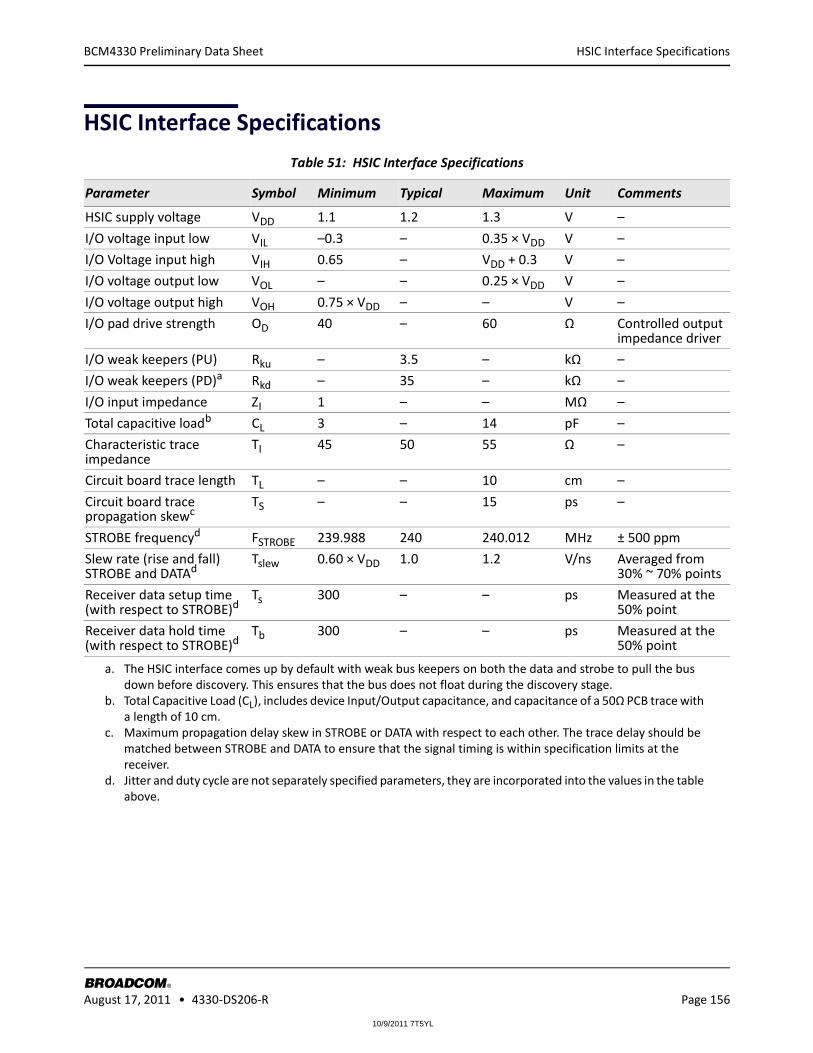
10/9/2011 7T5YL
HSIC Interface Specifications
BROADCOM August 17, 2011 • 4330-DS206-R Page 156
®
BCM4330 Preliminary Data Sheet
HSIC Interface Specifications
Table 51: HSIC Interface Specifications
Parameter Symbol Minimum Typical Maximum Unit Comments
HSIC supply voltage VDD 1.1 1.2 1.3 V –
I/O voltage input low VIL –0.3 – 0.35 × VDD V –
I/O Voltage input high VIH 0.65 – VDD + 0.3 V –
I/O voltage output low VOL – – 0.25 × VDD V –
I/O voltage output high VOH 0.75 × VDD – – V –
I/O pad drive strength OD 40 – 60 Ω Controlled output impedance driver
I/O weak keepers (PU) Rku – 3.5 – kΩ –
I/O weak keepers (PD)a
a. The HSIC interface comes up by default with weak bus keepers on both the data and strobe to pull the bus down before discovery. This ensures that the bus does not float during the discovery stage.
Rkd – 35 – kΩ –
I/O input impedance ZI 1 – – MΩ –
Total capacitive loadb
b. Total Capacitive Load (CL), includes device Input/Output capacitance, and capacitance of a 50Ω PCB trace with a length of 10 cm.
CL 3 – 14 pF –
Characteristic trace impedance
TI 45 50 55 Ω –
Circuit board trace length TL – – 10 cm –
Circuit board trace propagation skewc
c. Maximum propagation delay skew in STROBE or DATA with respect to each other. The trace delay should be matched between STROBE and DATA to ensure that the signal timing is within specification limits at the receiver.
TS – – 15 ps –
STROBE frequencyd
d. Jitter and duty cycle are not separately specified parameters, they are incorporated into the values in the table above.
FSTROBE 239.988 240 240.012 MHz ± 500 ppm
Slew rate (rise and fall) STROBE and DATAd
Tslew 0.60 × VDD 1.0 1.2 V/ns Averaged from 30% ~ 70% points
Receiver data setup time (with respect to STROBE)d
Ts 300 – – ps Measured at the 50% point
Receiver data hold time (with respect to STROBE)d
Tb 300 – – ps Measured at the 50% point

10/9/2011 7T5YL
JTAG Timing
BROADCOM August 17, 2011 • 4330-DS206-R Page 157
®
BCM4330 Preliminary Data Sheet
JTAG Timing
Table 52: JTAG Timing Characteristics
Signal Name PeriodOutput Maximum
Output Minimum Setup Hold
TCK 125 ns – – – –
TDI – – – 20 ns 0 ns
TMS – – – 20 ns 0 ns
TDO – 100 ns 0 ns – –
JTAG_TRST 250 ns – – – –

10/9/2011 7T5YL
Power-Up Sequence and Timing
BROADCOM August 17, 2011 • 4330-DS206-R Page 158
®
BCM4330 Preliminary Data Sheet
Section 23: Power-Up Sequence and T iming
Sequencing of Reset and Regulator Control SignalsThe BCM4330 has three signals that allow the host to control power consumption by enabling or disabling the Bluetooth, WLAN, and internal regulator blocks. These signals are described below. Additionally, diagrams are provided to indicate proper sequencing of the signals for various operational states (see Figure 47 on page 159, Figure 48 on page 160, Figure 49 on page 160 and Figure 50 on page 161). The timing values indicated are the minimum required values; longer delays are also acceptable.
Also note that the reset requirements for the Bluetooth core are also applicable for the FM core. In other words, if FM is to be used, then the Bluetooth core must be enabled.
Note: The WL_REG_ON and BT_REG_ON signals are ORed in the BCM4330. The diagrams show both signals going high at the same time (as would be the case if both REG signals were controlled by a single host GPIO). If two independent host GPIOs are used (one for WL_REG_ON and one for BT_REG_ON), then only one of the two signals needs to be high to enable the BCM4330 regulators.
Note: The BCM4330 has an internal power-on reset (POR) circuit. The device will be held in reset for a maximum of 110 ms after VDDC and VDDIO have both passed the 0.6V threshold. Wait at least 150 ms after VDDC and VDDIO are available before initiating SDIO accesses. The external reset signals are logically ORed with this POR. So if either the internal POR or one of the external resets is asserted, the device will be in reset. If VDDIO goes LOW, all regulators (including bandgap reference) will be powered OFF immediately, regardless of the status of the WL_REG_ON, BT_REG_ON, and EXT_SMPS_REQ pins.

10/9/2011 7T5YL
Sequencing of Reset and Regulator Control Signals
BROADCOM August 17, 2011 • 4330-DS206-R Page 159
®
BCM4330 Preliminary Data Sheet
Description of Control Signals• WL_REG_ON: Used by the PMU to power up the WLAN section. It is also OR-gated with the BT_REG_ON
input to control the internal BCM4330 regulators. When this pin is high, the regulators are enabled and the WLAN section is out of reset. When this pin is low the WLAN section is in reset. A “warm” WLAN reset can be initiated by driving WL_REG_ON low for at least 10 microseconds (see Figure 51 on page 161). If both the BT_REG_ON and WL_REG_ON pins are low, the regulators are disabled. Logic High Level: 1.08V–3.6V. 200k pull-down resistor included.
• BT_REG_ON: Used by the PMU (OR-gated with WL_REG_ON) to power up the internal BCM4330 regulators. If both the BT_REG_ON and WL_REG_ON pins are low, the regulators are disabled. Logic High Level: 1.08V–3.6V. 200k pull-down resistor included.
• BT_RST_N: Low asserting reset for Bluetooth and FM only. This pin has no effect on WLAN and does not control any PMU functions. This pin must be driven high or low (not left floating).
In addition, two other input signals control PMU modes:
• When EXT_SMPS_REQ is pulled high, it forces CBUCK to stay on, even when the other regulators are shut down by WL_REG_ON or BT_REG_ON.
• When WLAN and/or Bluetooth are out of reset and EXT_SMPS_REQ is high, then pulling EXT_PWM_REQ high makes CBUCK go into PWM mode, even if internal settings from WLAN and/or Bluetooth are requesting burst mode. During such contention, the request for the higher-power mode wins.
Control Signal Timing Diagrams
Figure 47: WLAN = ON, Bluetooth = ON
32.678 kHz Sleep Clock
VBAT
VDDIO
WL_REG_ON
BT_REG_ON
BT_RST_N
90% of VH
~ 2 Sleep cycles

10/9/2011 7T5YL
Sequencing of Reset and Regulator Control Signals
BROADCOM August 17, 2011 • 4330-DS206-R Page 160
®
BCM4330 Preliminary Data Sheet
Figure 48: WLAN = OFF, Bluetooth = OFF
Figure 49: WLAN = ON, Bluetooth = OFF
32.678 kHz Sleep Clock
VBAT
VDDIO
WL_REG_ON
BT_REG_ON
BT_RST_N
32.678 kHz Sleep Clock
VBAT
VDDIO
WL_REG_ON
BT_REG_ON
BT_RST_N
90% of VH
~ 2 Sleep cycles

10/9/2011 7T5YL
Sequencing of Reset and Regulator Control Signals
BROADCOM August 17, 2011 • 4330-DS206-R Page 161
®
BCM4330 Preliminary Data Sheet
Figure 50: WLAN = OFF, Bluetooth = ON
Figure 51: WLAN Warm Reset
32.678 kHz Sleep Clock
VBAT
VDDIO
WL_REG_ON
BT_REG_ON
BT_RST_N
90% of VH
~ 2 Sleep cycles
32.678 kHz Sleep Clock
VBAT
VDDIO
WL_REG_ON
BT_REG_ON
90% of VH
~ 2 Sleep cycles10 µs min
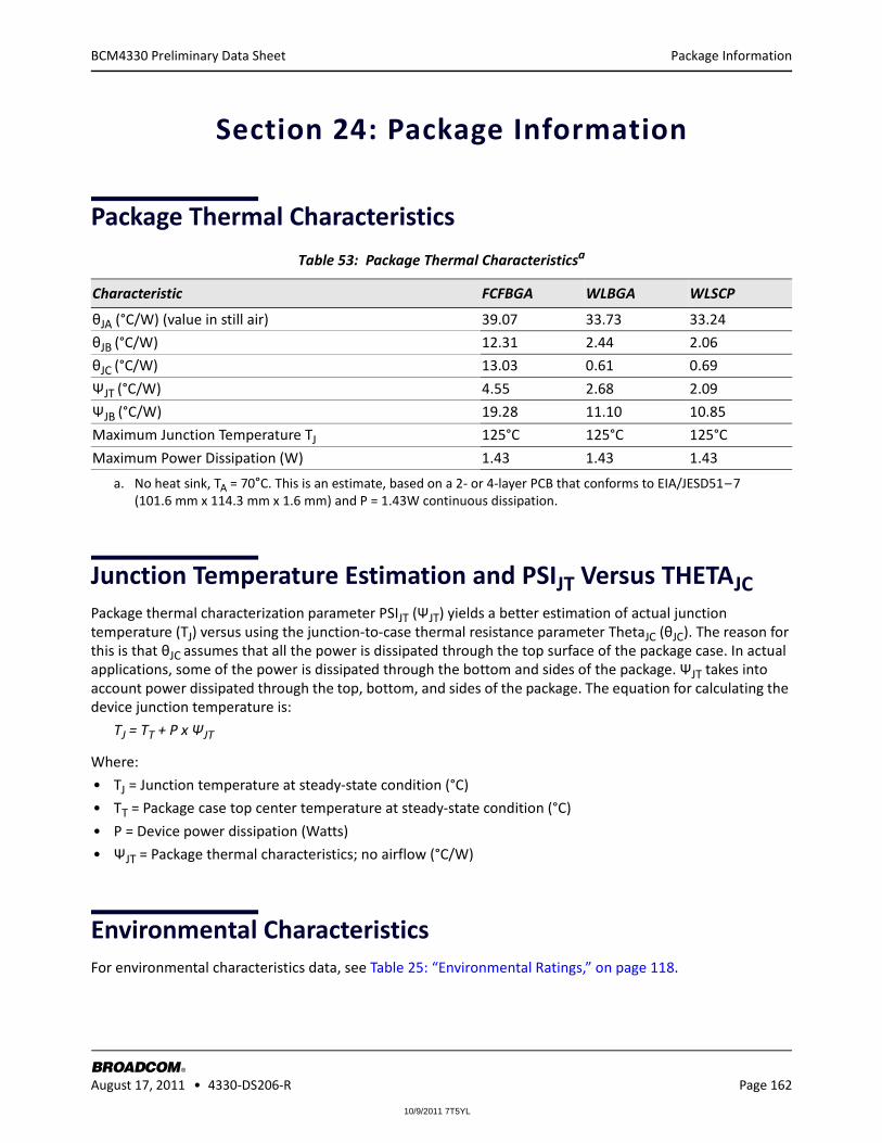
10/9/2011 7T5YL
Package Information
BROADCOM August 17, 2011 • 4330-DS206-R Page 162
®
BCM4330 Preliminary Data Sheet
Section 24: Package Information
Package Thermal Characteristics
Junction Temperature Estimation and PSIJT Versus THETAJCPackage thermal characterization parameter PSIJT (ΨJT) yields a better estimation of actual junction temperature (TJ) versus using the junction-to-case thermal resistance parameter ThetaJC (θJC). The reason for this is that θJC assumes that all the power is dissipated through the top surface of the package case. In actual applications, some of the power is dissipated through the bottom and sides of the package. ΨJT takes into account power dissipated through the top, bottom, and sides of the package. The equation for calculating the device junction temperature is:
TJ = TT + P x ΨJT
Where:
• TJ = Junction temperature at steady-state condition (°C)
• TT = Package case top center temperature at steady-state condition (°C)
• P = Device power dissipation (Watts)
• ΨJT = Package thermal characteristics; no airflow (°C/W)
Environmental CharacteristicsFor environmental characteristics data, see Table 25: “Environmental Ratings,” on page 118.
Table 53: Package Thermal Characteristicsa
a. No heat sink, TA = 70°C. This is an estimate, based on a 2- or 4-layer PCB that conforms to EIA/JESD51 – 7 (101.6 mm x 114.3 mm x 1.6 mm) and P = 1.43W continuous dissipation.
Characteristic FCFBGA WLBGA WLSCP
θJA (°C/W) (value in still air) 39.07 33.73 33.24
θJB (°C/W) 12.31 2.44 2.06
θJC (°C/W) 13.03 0.61 0.69
ΨJT (°C/W) 4.55 2.68 2.09
ΨJB (°C/W) 19.28 11.10 10.85
Maximum Junction Temperature TJ 125°C 125°C 125°C
Maximum Power Dissipation (W) 1.43 1.43 1.43
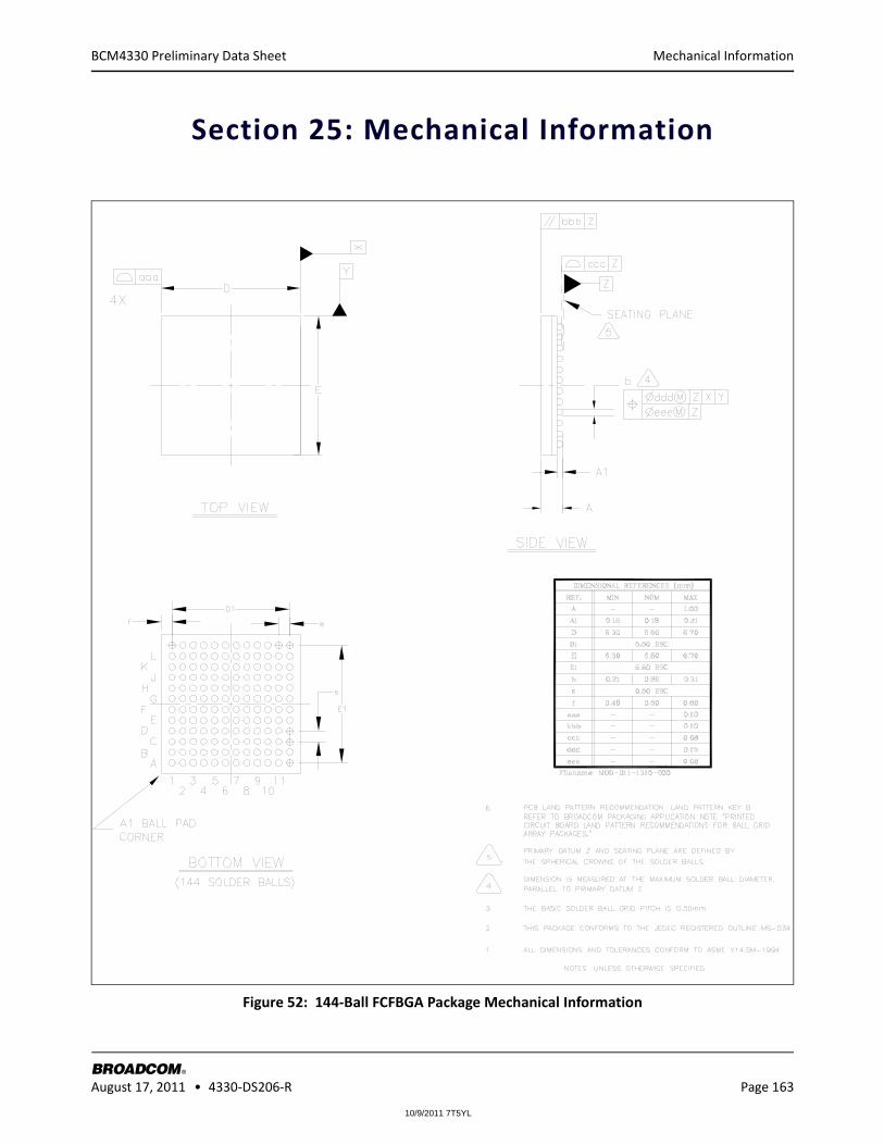
10/9/2011 7T5YL
Mechanical Information
BROADCOM August 17, 2011 • 4330-DS206-R Page 163
®
BCM4330 Preliminary Data Sheet
Section 25: Mechanical Information
Figure 52: 144-Ball FCFBGA Package Mechanical Information

10/9/2011 7T5YL
Mechanical Information
BROADCOM August 17, 2011 • 4330-DS206-R Page 164
®
BCM4330 Preliminary Data Sheet
Figure 53: 133-Ball WLBGA Package Mechanical Information

10/9/2011 7T5YL
Mechanical Information
BROADCOM August 17, 2011 • 4330-DS206-R Page 165
®
BCM4330 Preliminary Data Sheet
Figure 54: 225-Bump WLCSP Package Mechanical Information
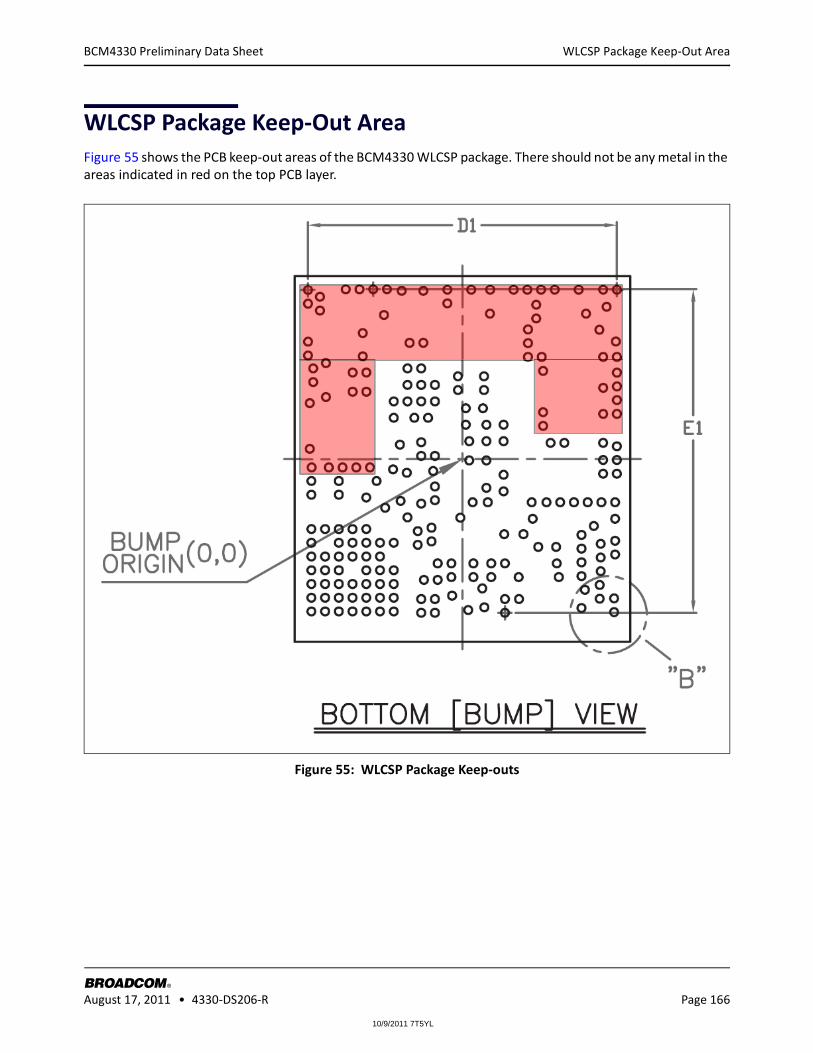
10/9/2011 7T5YL
WLCSP Package Keep-Out Area
BROADCOM August 17, 2011 • 4330-DS206-R Page 166
®
BCM4330 Preliminary Data Sheet
WLCSP Package Keep-Out AreaFigure 55 shows the PCB keep-out areas of the BCM4330 WLCSP package. There should not be any metal in the areas indicated in red on the top PCB layer.
Figure 55: WLCSP Package Keep-outs

10/9/2011 7T5YL
Ordering Information
BROADCOM August 17, 2011 • 4330-DS206-R Page 167
®
BCM4330 Preliminary Data Sheet
Section 26: Ordering Information
Table 54: Ordering Information
Part Number Package Description
Operating Ambient Temp
BCM4330FB2KFFBG 144 ball FCFBGA (6.5 mm x 6.5 mm, 0.5 mm pitch)
Single-band WLAN + BT 4.0 + FM RX – 30°C to +85°C
BCM4330FKUBG 133 ball WLBGA (4.89 mm x 5.33 mm, 0.4 mm pitch)
Single-band WLAN + BT 4.0 + FM RX – 30°C to +85°C
BCM4330SB2KUBG 133 ball WLBGA + BSP (4.89 mm x 5.33 mm, 0.4 mm pitch)
Single-band WLAN + BT 4.0 – 30°C to +85°C
BCM4330FKWBG 225 bump WLCSP (4.89 mm x 5.33 mm, 0.2 mm pitch)
Single-band WLAN + BT 4.0 + FM RX – 30°C to +85°C
BCM4330GKUBG 133 ball WLBGA (4.89 mm x 5.33 mm, 0.4 mm pitch)
Single-band WLAN + BT 4.0 – 30°C to +85°C
BCM4330XB2KFFBG 144 ball FCFBGA (6.5 mm x 6.5 mm, 0.5 mm pitch)
Dual-band WLAN + BT 4.0 + FM – 30°C to +85°C
BCM4330XKUBG 133 ball WLBGA (4.89 mm x 5.33 mm, 0.4 mm pitch)
Dual-band WLAN + BT 4.0 + FM – 30°C to +85°C
BCM4330HB2KUBG 133 ball WLBGA + BSP (4.89 mm x 5.33 mm, 0.4 mm pitch)
Dual-band WLAN + BT 4.0 + FM – 30°C to +85°C
BCM4330XKWBG 225 bump WLCSP (4.89 mm x 5.33 mm, 0.2 mm pitch)
Dual-band WLAN + BT 4.0 + FM – 30°C to +85°C
10/9/2011 7T5YL
®
Phone: 949-926-5000Fax: 949-926-5203E-mail: [email protected]: www.broadcom.com
BROADCOM CORPORATION5300 California AvenueIrvine, CA 92617© 2011 by BROADCOM CORPORATION. All rights reserved.
4330-DS206-R August 17, 2011
Broadcom® Corporation reserves the right to make changes without further notice to any products or data herein to improve reliability, function, or design.
Information furnished by Broadcom Corporation is believed to be accurate and reliable. However, Broadcom Corporation does not assume any liability arising out of the application or use of this information, nor the application or use of any product or circuit described herein, neither does it convey any license under its patent rights nor the rights of others.
BCM4330 Preliminary Data Sheet