bga736l16 - digi-key sheets/infineon pdfs/bga736l16.… · data sheet 3 v2.1, 2008-07-03 bga736l16...
TRANSCRIPT

BGA736L16Tri-Band HSDPA LNA(2100, 1900/2100, 800/900 MHz)
Data Sheet, V2.1, July 2008
RF & Protect ion Devices

Edition 2008-07-03Published byInfineon Technologies AG81726 München, Germany© Infineon Technologies AG 2009.All Rights Reserved.
Legal DisclaimerThe information given in this document shall in no event be regarded as a guarantee of conditions or characteristics (“Beschaffenheitsgarantie”). With respect to any examples or hints given herein, any typical values stated herein and/or any information regarding the application of the device, Infineon Technologies hereby disclaims any and all warranties and liabilities of any kind, including without limitation warranties of non-infringement of intellectual property rights of any third party.
InformationFor further information on technology, delivery terms and conditions and prices please contact your nearest Infineon Technologies Office (www.infineon.com).
WarningsDue to technical requirements components may contain dangerous substances. For information on the types in question please contact your nearest Infineon Technologies Office.Infineon Technologies Components may only be used in life-support devices or systems with the express written approval of Infineon Technologies, if a failure of such components can reasonably be expected to cause the failure of that life-support device or system, or to affect the safety or effectiveness of that device or system. Life support devices or systems are intended to be implanted in the human body, or to support and/or maintain and sustain and/or protect human life. If they fail, it is reasonable to assume that the health of the user or other persons may be endangered.

Data Sheet 3 V2.1, 2008-07-03
BGA736L16 - Tri-Band HSDPA LNA
BGA736L16Revision History: 2008-07-03, V2.1Previous Version: 2008-02-27, V2.0Page Subjects (major changes since last revision)5, 6 Updated HBM ESD protection11 Added RF characteristics for UMTS band VIII13 Added RF characteristics for UMTS band IV39 Added application circuit schematic for UMTS bands I, IV and VIIIall Updated values for high and mid gain currents

Data Sheet 4 V2.1, 2008-07-03
BGA736L16 - Tri-Band HSDPA LNA
Table of Contents . . . . . . . . . . . . . . . . . . . . . . . . . . . . . . . . . . . . . . . . . . . . . . . . . . . . . . . . . . . . . . . . 4
1 Description . . . . . . . . . . . . . . . . . . . . . . . . . . . . . . . . . . . . . . . . . . . . . . . . . . . . . . . . . . . . . . . . . . . . . 5
2 Electrical Characteristics . . . . . . . . . . . . . . . . . . . . . . . . . . . . . . . . . . . . . . . . . . . . . . . . . . . . . . . . . . 62.1 Absolute Maximum Ratings . . . . . . . . . . . . . . . . . . . . . . . . . . . . . . . . . . . . . . . . . . . . . . . . . . . . . . . . . 62.2 Thermal Resistance . . . . . . . . . . . . . . . . . . . . . . . . . . . . . . . . . . . . . . . . . . . . . . . . . . . . . . . . . . . . . . . 62.3 ESD Integrity . . . . . . . . . . . . . . . . . . . . . . . . . . . . . . . . . . . . . . . . . . . . . . . . . . . . . . . . . . . . . . . . . . . . . 62.4 DC Characteristics . . . . . . . . . . . . . . . . . . . . . . . . . . . . . . . . . . . . . . . . . . . . . . . . . . . . . . . . . . . . . . . . 72.5 Band Select / Gain Control Truth Table . . . . . . . . . . . . . . . . . . . . . . . . . . . . . . . . . . . . . . . . . . . . . . . . 72.6 Supply current characteristics; TA = 25 °C . . . . . . . . . . . . . . . . . . . . . . . . . . . . . . . . . . . . . . . . . . . . . . 82.7 Logic Signal Characteristics; TA = 25 °C . . . . . . . . . . . . . . . . . . . . . . . . . . . . . . . . . . . . . . . . . . . . . . . 92.8 Switching Times . . . . . . . . . . . . . . . . . . . . . . . . . . . . . . . . . . . . . . . . . . . . . . . . . . . . . . . . . . . . . . . . . . 92.9 Measured RF Characteristics Low Band . . . . . . . . . . . . . . . . . . . . . . . . . . . . . . . . . . . . . . . . . . . . . . 102.9.1 Measured RF Characteristics UMTS Band V . . . . . . . . . . . . . . . . . . . . . . . . . . . . . . . . . . . . . . . . . 102.9.2 Measured RF Characteristics UMTS Band VIII . . . . . . . . . . . . . . . . . . . . . . . . . . . . . . . . . . . . . . . . 112.10 Measured RF Characteristics Mid Band . . . . . . . . . . . . . . . . . . . . . . . . . . . . . . . . . . . . . . . . . . . . . . . 122.10.1 Measured RF Characteristics UMTS Band II . . . . . . . . . . . . . . . . . . . . . . . . . . . . . . . . . . . . . . . . . . 122.10.2 Measured RF Characteristics UMTS Band IV . . . . . . . . . . . . . . . . . . . . . . . . . . . . . . . . . . . . . . . . . 132.11 Measured RF Characteristics High Band . . . . . . . . . . . . . . . . . . . . . . . . . . . . . . . . . . . . . . . . . . . . . . 142.11.1 Measured RF Characteristics UMTS Band I . . . . . . . . . . . . . . . . . . . . . . . . . . . . . . . . . . . . . . . . . . 142.12 Measured Performance Low Band High Gain Mode vs. Frequency . . . . . . . . . . . . . . . . . . . . . . . . . . 152.13 Measured Performance Low Band High Gain Mode vs. Temperature . . . . . . . . . . . . . . . . . . . . . . . . 162.14 Measured Performance Low Band Mid Gain Mode vs. Frequency . . . . . . . . . . . . . . . . . . . . . . . . . . 172.15 Measured Performance Low Band Mid Gain Mode vs. Temperature . . . . . . . . . . . . . . . . . . . . . . . . . 192.16 Measured Performance Low Band Low Gain Mode vs. Frequency . . . . . . . . . . . . . . . . . . . . . . . . . . 202.17 Measured Performance Low Band Low Gain Mode vs. Temperature . . . . . . . . . . . . . . . . . . . . . . . . 212.18 Measured Performance Mid Band High Gain Mode vs. Frequency . . . . . . . . . . . . . . . . . . . . . . . . . . 222.19 Measured Performance Mid Band High Gain Mode vs. Temperature . . . . . . . . . . . . . . . . . . . . . . . . 242.20 Measured Performance Mid Band Mid Gain Mode vs. Frequency . . . . . . . . . . . . . . . . . . . . . . . . . . . 252.21 Measured Performance Mid Band Mid Gain Mode vs. Temperature . . . . . . . . . . . . . . . . . . . . . . . . . 262.22 Measured Performance Mid Band Low Gain Mode vs. Frequency . . . . . . . . . . . . . . . . . . . . . . . . . . 272.23 Measured Performance Mid Band Low Gain Mode vs. Temperature . . . . . . . . . . . . . . . . . . . . . . . . . 292.24 Measured Performance High Band High Gain Mode vs. Frequency . . . . . . . . . . . . . . . . . . . . . . . . . 302.25 Measured Performance High Band High Gain Mode vs. Temperature . . . . . . . . . . . . . . . . . . . . . . . 312.26 Measured Performance High Band Mid Gain Mode vs. Frequency . . . . . . . . . . . . . . . . . . . . . . . . . . 322.27 Measured Performance High Band Mid Gain Mode vs. Temperature . . . . . . . . . . . . . . . . . . . . . . . . 342.28 Measured Performance High Band Low Gain Mode vs. Frequency . . . . . . . . . . . . . . . . . . . . . . . . . . 352.29 Measured Performance High Band Low Gain Mode vs. Temperature . . . . . . . . . . . . . . . . . . . . . . . . 36
3 Application Circuit and Block Diagram . . . . . . . . . . . . . . . . . . . . . . . . . . . . . . . . . . . . . . . . . . . . . 383.1 UMTS bands I, II and V Application Circuit Schematic . . . . . . . . . . . . . . . . . . . . . . . . . . . . . . . . . . . . 383.2 UMTS bands I, IV and VIII Application Circuit Schematic . . . . . . . . . . . . . . . . . . . . . . . . . . . . . . . . . 393.3 Pin Definition . . . . . . . . . . . . . . . . . . . . . . . . . . . . . . . . . . . . . . . . . . . . . . . . . . . . . . . . . . . . . . . . . . . . 403.4 Application Board . . . . . . . . . . . . . . . . . . . . . . . . . . . . . . . . . . . . . . . . . . . . . . . . . . . . . . . . . . . . . . . . 41
4 Physical Characteristics . . . . . . . . . . . . . . . . . . . . . . . . . . . . . . . . . . . . . . . . . . . . . . . . . . . . . . . . . 434.1 Package Footprint . . . . . . . . . . . . . . . . . . . . . . . . . . . . . . . . . . . . . . . . . . . . . . . . . . . . . . . . . . . . . . . . 434.2 Package Dimensions . . . . . . . . . . . . . . . . . . . . . . . . . . . . . . . . . . . . . . . . . . . . . . . . . . . . . . . . . . . . . 44
Table of Contents

Data Sheet 5 V2.1, 2008-07-03
BGA736L16 - Tri-Band HSDPA LNADescription
1 DescriptionThe BGA736L16 is a highly flexible, tri-gain mode, and tri-band (2100, 1900/2100, 800/900 MHz) MMIC low noiseamplifier for worldwide use. Based on Infineon’s proprietary and cost-effective SiGe:C technology, the BGA736L16features dynamic gain control, temperature stabilization, standby mode, and 2 kV ESD protection on-chip andmatching off chip.While two gain modes are common in W-CDMA systems, a third gain mode has been introduced to reduce theLNA gain just enough to pass adjacent channel tests without compromising on HSDPA performance. The1900 MHz path can be converted into a 2100 MHz path and vice versa by optimizing the input matching and usingan additional external output matching network. This document specifies device performance for the bandcombinations - UMTS bands I / II / V and UMTS bands I / IV / VIII.
Figure 1 Block diagram of triple-band LNA
Features• Gain: 16 / 3 / -8 dB in high / mid / low gain mode• Noise figure: 1.1 dB in high gain mode• Supply current: 5.3 / 5.3 / 0.85 mA in high / mid / low gain modes• Standby mode current consumption < 2 µA• Outputs internally matched to 50 Ω• 2 kV HBM ESD protection• Low external component count• Small leadless TSLP-16-1 package (2.3 x 2.3 x 0.39 mm)• Pb-free (RoHS compliant) package
TSLP-16-1 package
Type Package Marking ChipBGA736L16 PG-TSLP-16-1 BGA736 T1540

Data Sheet 6 V2.1, 2008-07-03
BGA736L16 - Tri-Band HSDPA LNAElectrical Characteristics
Absolute Maximum Ratings
2 Electrical Characteristics
2.1 Absolute Maximum Ratings
2.2 Thermal Resistance
2.3 ESD Integrity
Table 1 Absolute Maximum RatingsParameter Symbol Values Unit Note / Test Condition
Min. Max.Supply voltage VCC -0.3 3.6 VSupply current ICC 10 mAPin voltage VPIN -0.3 VCC +0.3 V All pins except RF input pinsPin voltage RF input pins VRFIN -0.3 0.9 VRF input power PRFIN 4 dBmJunction temperature Tj 150 °CAmbient temperature range TA -30 85 °CStorage temperature range TSTG -65 150 °C
Table 2 Thermal ResistanceParameter Symbol Value Unit Note / Test ConditionsThermal resistance junction to soldering point
RthJS ≤ 110 K/W
Table 3 ESD IntegrityParameter Symbol Value Unit Note / Test Conditions
Typ.ESD hardness HBM1)
1) According to JESD22-A114VESD-HBM 2000 V All pins

BGA736L16 - Tri-Band HSDPA LNAElectrical Characteristics
DC Characteristics
Data Sheet 7 V2.1, 2008-07-03
2.4 DC Characteristics
2.5 Band Select / Gain Control Truth Table
Table 4 DC Characteristics, TA = 25 °CParameter Symbol Values Unit Note / Test Condition
Min. Typ. Max.Supply voltage VCC 2.7 2.8 3.0 VSupply current high and mid gain mode
-30°C25°C85°C
ICCHGICCMG
4.35.36.4
mAmAmA
All bandsSupply current is proportional to absolute temperature
Supply current low gain mode
ICCLG 850 µA All bands
Supply current standby mode
ICCOFF 0.1 2 µA
Logic level high VHI 1.5 2.8 V VEN1 and VEN2Logic level low VLOW 0.0 0.5 VLogic currents VEN IENL 0.2 µA VEN1 and VEN2
IENH 10.0 µALogic currents VGS IGSL 0.1 µA VGS
IGSH 5.0 µA
Table 5 Band Select Truth Table, VCC = 2.8 VHigh band Mid band Low band Standby mode
VEN1 H H L LVEN2 H L H L
Table 6 Gain Control Truth Table, VCC = 2.8 VHigh Gain Mid Gain Low Gain
VGS1 H H LVGS2 L H L

Data Sheet 8 V2.1, 2008-07-03
BGA736L16 - Tri-Band HSDPA LNAElectrical Characteristics
Supply current characteristics; TA = 25 °C
2.6 Supply current characteristics; TA = 25 °CSupply current high / mid gain mode versus reference resistor RREF (see Figure 2 on page 38 for referenceresistor; low gain mode supply current is independent of reference resistor).
Supply Current Highband ICC = f (RREF)VCC = 2.8 V
Supply Current Midband ICC = f (RREF)VCC = 2.8 V
Supply Current Lowband ICC = f (RREF)VCC = 2.8 V
1 10 1002
3
4
5
6
7
8
9
RREF
[kΩ]
Icc
[mA
]
1 10 1002
3
4
5
6
7
8
9
RREF
[kΩ]
Icc
[mA
]
1 10 1002
3
4
5
6
7
8
9
RREF
[kΩ]
Icc
[mA
]

BGA736L16 - Tri-Band HSDPA LNAElectrical Characteristics
Logic Signal Characteristics; TA = 25 °C
Data Sheet 9 V2.1, 2008-07-03
2.7 Logic Signal Characteristics; TA = 25 °CCurrent consumption of logic inputs VEN1, VEN2, VGS1, VGS2
2.8 Switching Times
Logic Currents IEN1,2 = f (VEN1,2)VCC = 2.8 V
Logic Currents IGS1,2 = f (VGS1,2)VCC = 2.8 V
Table 7 Typical switching times; TA = -30 ... 85 °CParameter Symbol Values Unit Note / Test Condition
Min. Typ. Max.Settling time gainstep tGS 1 µs Switching from any gain
mode to a different gain mode; all bands
Settling time bandselect tBS 1.6 µs Switching from any band to a different band; all gain modes
0 0.5 1 1.5 2 2.5 30
2
4
6
8
10
12
VEN1,2
[V]
I EN
1,2 [µ
A]
0 0.5 1 1.5 2 2.5 30
2
4
6
VGS1,2
[V]
I GS
1,2 [µ
A]

Data Sheet 10 V2.1, 2008-07-03
BGA736L16 - Tri-Band HSDPA LNAElectrical Characteristics
Measured RF Characteristics Low Band
2.9 Measured RF Characteristics Low Band
2.9.1 Measured RF Characteristics UMTS Band V
Table 8 Typical Characteristics 800 MHz Band, TA = 25 °C, VCC = 2.8 V, RREF = 8.2 kΩ
Parameter Symbol Values Unit Note / Test ConditionMin. Typ. Max.
Pass band range 869 894 MHzCurrent consumption ICCHG 5.20 mA High gain mode
ICCMG 5.20 mA Mid gain modeICCLG 0.85 mA Low gain mode
Gain S21HG 15.5 dB High gain modeS21MG 3.0 dB Mid gain modeS21LG -8.9 dB Low gain mode
Reverse Isolation1)
1) Verified by random sampling; not 100% RF tested
S12HG -38 dB High gain modeS12MG -40 dB Mid gain modeS12LG -9 dB Low gain mode
Noise figure NFHG 1.1 dB High gain modeNFMG 2.4 dB Mid gain modeNFLG 9.0 dB Low gain mode
Input return loss1) S11HG -14 dB 50 Ω, high gain modeS11MG -12 dB 50 Ω, mid gain modeS11LG -10 dB 50 Ω, low gain mode
Output return loss1) S22HG -20 dB 50 Ω, high gain modeS22MG -22 dB 50 Ω, mid gain modeS22LG -18 dB 50 Ω, low gain mode
Stability factor2)
2) Not tested in production; guaranteed by device design
k >3.1 DC to 10 GHz; all gain modes
Input compression point1) IP1dBHG -11 dBm High gain modeIP1dBMG -10 dBm Mid gain modeIP1dBLG -12 dBm Low gain mode
Inband IIP31)
f1 - f2 = 1 MHz Pf1 = Pf2 = -25 dBm
IIP3HGIIP3MGIIP3LG
-5-5-3
dBm High gain modeMid gain modeLow gain mode

BGA736L16 - Tri-Band HSDPA LNAElectrical Characteristics
Measured RF Characteristics Low Band
Data Sheet 11 V2.1, 2008-07-03
2.9.2 Measured RF Characteristics UMTS Band VIII
Table 9 Typical Characteristics 900 MHz Band, TA = 25 °C, VCC = 2.8 V, RREF = 8.2 kΩ
Parameter Symbol Values Unit Note / Test ConditionMin. Typ. Max.
Pass band range 925 960 MHzCurrent consumption ICCHG 5.20 mA High gain mode
ICCMG 5.20 mA Mid gain modeICCLG 0.85 mA Low gain mode
Gain S21HG 15.2 dB High gain modeS21MG 2.8 dB Mid gain modeS21LG -8.8 dB Low gain mode
Reverse Isolation1)
1) Verified by random sampling; not 100% RF tested
S12HG -37 dB High gain modeS12MG -39 dB Mid gain modeS12LG -9 dB Low gain mode
Noise figure NFHG 1.2 dB High gain modeNFMG 2.6 dB Mid gain modeNFLG 9.0 dB Low gain mode
Input return loss1) S11HG -14 dB 50 Ω, high gain modeS11MG -12 dB 50 Ω, mid gain modeS11LG -11 dB 50 Ω, low gain mode
Output return loss1) S22HG -20 dB 50 Ω, high gain modeS22MG -19 dB 50 Ω, mid gain modeS22LG -19 dB 50 Ω, low gain mode
Stability factor2)
2) Not tested in production; guaranteed by device design
k >3.4 DC to 10 GHz; all gain modes
Input compression point1) IP1dBHG -9 dBm High gain modeIP1dBMG -5 dBm Mid gain modeIP1dBLG -11 dBm Low gain mode
Inband IIP31)
f1 - f2 = 1 MHz Pf1 = Pf2 = -25 dBm
IIP3HGIIP3MGIIP3LG
-5-5-3
dBm High gain modeMid gain modeLow gain mode

Data Sheet 12 V2.1, 2008-07-03
BGA736L16 - Tri-Band HSDPA LNAElectrical Characteristics
Measured RF Characteristics Mid Band
2.10 Measured RF Characteristics Mid Band
2.10.1 Measured RF Characteristics UMTS Band II
Table 10 Typical Characteristics 1900 MHz Band, TA = 25 °C, VCC = 2.8 V, RREF = 8.2 kΩ
Parameter Symbol Values Unit Note / Test ConditionMin. Typ. Max.
Pass band range 1930 1990 MHzCurrent consumption ICCHG 5.30 mA High gain mode
ICCMG 5.30 mA Mid gain modeICCLG 0.85 mA Low gain mode
Gain S21HG 16.1 dB High gain modeS21MG 2.7 dB Mid gain modeS21LG -8.1 dB Low gain mode
Reverse Isolation1)
1) Verified by random sampling; not 100% RF tested
S12HG -35 dB High gain modeS12MG -36 dB Mid gain modeS12LG -8 dB Low gain mode
Noise figure NFHG 1.0 dB High gain modeNFMG 2.3 dB Mid gain modeNFLG 7.8 dB Low gain mode
Input return loss1) S11HG -15 dB 50 Ω, high gain modeS11MG -12 dB 50 Ω, mid gain modeS11LG -11 dB 50 Ω, low gain mode
Output return loss1) S22HG -19 dB 50 Ω, high gain modeS22MG -18 dB 50 Ω, mid gain modeS22LG -18 dB 50 Ω, low gain mode
Stability factor2)
2) Not tested in production; guaranteed by device design
k >2.6 DC to 10 GHz; all gain modes
Input compression point1) IP1dBHG -13 dBm High gain modeIP1dBMG -13 dBm Mid gain modeIP1dBLG -7 dBm Low gain mode
Inband IIP31)
f1 - f2 = 1 MHz Pf1 = Pf2 = -26 dBm
IIP3HGIIP3MGIIP3LG
-5-62
dBm High gain modeMid gain modeLow gain mode

BGA736L16 - Tri-Band HSDPA LNAElectrical Characteristics
Measured RF Characteristics Mid Band
Data Sheet 13 V2.1, 2008-07-03
2.10.2 Measured RF Characteristics UMTS Band IV
Table 11 Typical Characteristics 2100 MHz Band, TA = 25 °C, VCC = 2.8 V, RREF = 8.2 kΩ
Parameter Symbol Values Unit Note / Test ConditionMin. Typ. Max.
Pass band range 2110 2155 MHzCurrent consumption ICCHG 5.30 mA High gain mode
ICCMG 5.30 mA Mid gain modeICCLG 0.85 mA Low gain mode
Gain S21HG 15.3 dB High gain modeS21MG 2.3 dB Mid gain modeS21LG -7.5 dB Low gain mode
Reverse Isolation1)
1) Verified by random sampling; not 100% RF tested
S12HG -34 dB High gain modeS12MG -35 dB Mid gain modeS12LG -8 dB Low gain mode
Noise figure NFHG 1.1 dB High gain modeNFMG 2.7 dB Mid gain modeNFLG 7.5 dB Low gain mode
Input return loss1) S11HG -19 dB 50 Ω, high gain modeS11MG -14 dB 50 Ω, mid gain modeS11LG -12 dB 50 Ω, low gain mode
Output return loss1) S22HG -18 dB 50 Ω, high gain modeS22MG -17 dB 50 Ω, mid gain modeS22LG -15 dB 50 Ω, low gain mode
Stability factor2)
2) Not tested in production; guaranteed by device design
k >2.6 DC to 10 GHz; all gain modes
Input compression point1) IP1dBHG -12 dBm High gain modeIP1dBMG -12 dBm Mid gain modeIP1dBLG -6 dBm Low gain mode
Inband IIP31)
f1 - f2 = 1 MHz Pf1 = Pf2 = -26 dBm
IIP3HGIIP3MGIIP3LG
-5-62
dBm High gain modeMid gain modeLow gain mode

Data Sheet 14 V2.1, 2008-07-03
BGA736L16 - Tri-Band HSDPA LNAElectrical Characteristics
Measured RF Characteristics High Band
2.11 Measured RF Characteristics High Band
2.11.1 Measured RF Characteristics UMTS Band I
Table 12 Typical Characteristics 2100 MHz Band, TA = 25 °C, VCC = 2.8 V, RREF = 8.2 kΩ
Parameter Symbol Values Unit Note / Test ConditionMin. Typ. Max.
Pass band range 2110 2170 MHzCurrent consumption ICCHG 5.30 mA High gain mode
ICCMG 5.30 mA Mid gain modeICCLG 0.85 mA Low gain mode
Gain S21HG 16.2 dB High gain modeS21MG 2.3 dB Mid gain modeS21LG -8.0 dB Low gain mode
Reverse Isolation1)
1) Verified by random sampling; not 100% RF tested
S12HG -35 dB High gain modeS12MG -36 dB Mid gain modeS12LG -8 dB Low gain mode
Noise figure NFHG 1.0 dB High gain modeNFMG 2.6 dB Mid gain modeNFLG 7.9 dB Low gain mode
Input return loss1) S11HG -13 dB 50 Ω, high gain modeS11MG -12 dB 50 Ω, mid gain modeS11LG -10 dB 50 Ω, low gain mode
Output return loss1) S22HG -19 dB 50 Ω, high gain modeS22MG -24 dB 50 Ω, mid gain modeS22LG -14 dB 50 Ω, low gain mode
Stability factor2)
2) Not tested in production; guaranteed by device design
k >2.2 DC to 10 GHz; all gain modes
Input compression point1) IP1dBHG -13 dBm High gain modeIP1dBMG -13 dBm Mid gain modeIP1dBLG -7 dBm Low gain mode
Inband IIP31)
f1 - f2 = 1 MHz Pf1 = Pf2 = -27 dBm
IIP3HGIIP3MGIIP3LG
-5-52
dBm High gain modeMid gain modeLow gain mode

BGA736L16 - Tri-Band HSDPA LNAElectrical Characteristics
Measured Performance Low Band High Gain Mode vs. Frequency
Data Sheet 15 V2.1, 2008-07-03
2.12 Measured Performance Low Band High Gain Mode vs. FrequencyTA = 25 °C, VCC = 2.8 V, VGS1 = 2.8 V, VGS2 = 0 V, VEN1 = 0 V, VEN2 = 2.8 V, RREF = 8.2 kΩ
Power Gain |S21| = f( f ) Power Gain Wideband |S21| = f( f )
Matching |S11| = f( f ), |S22| = f( f ) Reverse Isolation |S12| = f( f )
0.86 0.87 0.88 0.89 0.914
14.5
15
15.5
16
16.5
17
Frequency [GHz]
Pow
er G
ain
[dB
]
−30°C
25°C
85°C
0 2 4 6 8 10−60
−50
−40
−30
−20
−10
0
10
20
Frequency [GHz]
Pow
er G
ain
[dB
]
0.86 0.87 0.88 0.89 0.9−35
−30
−25
−20
−15
−10
−5
0
Frequency [GHz]
|S11
|, |S
22| [
dB]
S11
S22
0 2 4 6 8 10−60
−50
−40
−30
−20
−10
0
Frequency [GHz]
|S12
| [dB
]

Data Sheet 16 V2.1, 2008-07-03
BGA736L16 - Tri-Band HSDPA LNAElectrical Characteristics
Measured Performance Low Band High Gain Mode vs. Temperature
2.13 Measured Performance Low Band High Gain Mode vs. TemperatureVCC = 2.8 V, VGS1 = 2.8 V, VGS2 = 0 V, VEN1 = 0 V, VEN2 = 2.8 V, RREF = 8.2 kΩ
Noise Figure NF = f( f ) Input Compression P1dB = f( f )
Power Gain |S21| = f(TA) Supply Current ICC = f(TA)
0.86 0.87 0.88 0.89 0.90.6
0.7
0.8
0.9
1
1.1
1.2
1.3
1.4
1.5
1.6
1.7
Frequency [GHz]
NF
[dB
]
0.86 0.87 0.88 0.89 0.9−15
−14
−13
−12
−11
−10
Frequency [GHz]
P1d
B [d
Bm
]
−40 −20 0 20 40 60 80 10014
14.5
15
15.5
16
16.5
17
17.5
18
TA [°C]
Pow
er G
ain
[dB
]
−40 −20 0 20 40 60 80 1004
4.5
5
5.5
6
6.5
7
TA [°C]
I CC
[mA
]

BGA736L16 - Tri-Band HSDPA LNAElectrical Characteristics
Measured Performance Low Band Mid Gain Mode vs. Frequency
Data Sheet 17 V2.1, 2008-07-03
2.14 Measured Performance Low Band Mid Gain Mode vs. FrequencyTA = 25 °C, VCC = 2.8 V, VGS1 = 2.8 V, VGS2 = 2.8 V, VEN1 = 0 V, VEN2 = 2.8 V, RREF = 8.2 kΩ
Noise Figure NF = f(TA) Input Compression P1dB = f(TA)
Power Gain |S21| = f( f ) Power Gain Wideband |S21| = f( f )
−40 −20 0 20 40 60 80 1000.6
0.7
0.8
0.9
1
1.1
1.2
1.3
1.4
1.5
1.6
1.7
TA [°C]
NF
[dB
]
−40 −20 0 20 40 60 80 100−15
−13
−11
−9
−7
−5
TA [°C]
P1d
B [d
Bm
]
0.86 0.87 0.88 0.89 0.91
1.5
2
2.5
3
3.5
4
Frequency [GHz]
Pow
er G
ain
[dB
]
−30°C
25°C
85°C
−30°C
25°C
85°C
−30°C
25°C
85°C
0 2 4 6 8 10−60
−50
−40
−30
−20
−10
0
10
Frequency [GHz]
Pow
er G
ain
[dB
]

Data Sheet 18 V2.1, 2008-07-03
BGA736L16 - Tri-Band HSDPA LNAElectrical Characteristics
Measured Performance Low Band Mid Gain Mode vs. Frequency
Matching |S11| = f( f ), |S22| = f( f ) Reverse Isolation |S12| = f( f )
Noise Figure NF = f( f ) Input Compression P1dB = f( f )
0.86 0.87 0.88 0.89 0.9−35
−30
−25
−20
−15
−10
−5
0
Frequency [GHz]
|S11
|, |S
22| [
dB]
S11
S22
0 2 4 6 8 10−60
−50
−40
−30
−20
−10
0
Frequency [GHz]
|S12
| [dB
]
0.86 0.87 0.88 0.89 0.91.5
1.7
1.9
2.1
2.3
2.5
2.7
2.9
3.1
3.3
3.5
Frequency [GHz]
NF
[dB
]
0.86 0.87 0.88 0.89 0.9−15
−14
−13
−12
−11
−10
−9
−8
Frequency [GHz]
P1d
B [d
Bm
]

BGA736L16 - Tri-Band HSDPA LNAElectrical Characteristics
Measured Performance Low Band Mid Gain Mode vs. Temperature
Data Sheet 19 V2.1, 2008-07-03
2.15 Measured Performance Low Band Mid Gain Mode vs. TemperatureVCC = 2.8 V, VGS1 = 2.8 V, VGS2 = 2.8 V, VEN1 = 0 V, VEN2 = 2.8 V, RREF = 8.2 kΩ
Power Gain |S21| = f(TA) Supply Current ICC = f(TA)
Noise Figure NF = f(TA) Input Compression P1dB = f(TA)
−40 −20 0 20 40 60 80 1000
0.5
1
1.5
2
2.5
3
3.5
4
4.5
5
TA [°C]
Pow
er G
ain
[dB
]
−40 −20 0 20 40 60 80 1004
4.5
5
5.5
6
6.5
7
TA [°C]
I CC
[mA
]
−40 −20 0 20 40 60 80 1001.5
1.7
1.9
2.1
2.3
2.5
2.7
2.9
3.1
3.3
3.5
TA [°C]
NF
[dB
]
−40 −20 0 20 40 60 80 100−17
−15
−13
−11
−9
−7
−5
TA [°C]
P1d
B [d
Bm
]

Data Sheet 20 V2.1, 2008-07-03
BGA736L16 - Tri-Band HSDPA LNAElectrical Characteristics
Measured Performance Low Band Low Gain Mode vs. Frequency
2.16 Measured Performance Low Band Low Gain Mode vs. FrequencyTA = 25 °C, VCC = 2.8 V, VGS1 = 0 V, VGS2 = 0 V, VEN1 = 0 V, VEN2 = 2.8 V, RREF = 8.2 kΩ
Power Gain |S21| = f( f ) Power Gain Wideband |S21| = f( f )
Matching |S11| = f( f ), |S22| = f( f ) Reverse Isolation |S12| = f( f )
0.86 0.87 0.88 0.89 0.9−11
−10.5
−10
−9.5
−9
−8.5
−8
−7.5
−7
Frequency [GHz]
Pow
er G
ain
[dB
]
85°C
−30°C, 25°C
85°C
−30°C, 25°C
85°C
−30°C, 25°C
0 2 4 6 8 10−70
−60
−50
−40
−30
−20
−10
0
Frequency [GHz]
Pow
er G
ain
[dB
]
0.86 0.87 0.88 0.89 0.9−35
−30
−25
−20
−15
−10
−5
0
Frequency [GHz]
|S11
|, |S
22| [
dB]
S11
S22
0 2 4 6 8 10−60
−50
−40
−30
−20
−10
0
Frequency [GHz]
|S12
| [dB
]
BGA736L16 - Tri-Band HSDPA LNAElectrical Characteristics
Measured Performance Low Band Low Gain Mode vs. Temperature
Data Sheet 21 V2.1, 2008-07-03
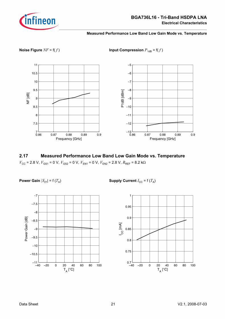
2.17 Measured Performance Low Band Low Gain Mode vs. TemperatureVCC = 2.8 V, VGS1 = 0 V, VGS2 = 0 V, VEN1 = 0 V, VEN2 = 2.8 V, RREF = 8.2 kΩ
Noise Figure NF = f( f ) Input Compression P1dB = f( f )
Power Gain |S21| = f (TA) Supply Current ICC = f (TA)
0.86 0.87 0.88 0.89 0.97
7.5
8
8.5
9
9.5
10
10.5
11
Frequency [GHz]
NF
[dB
]
0.86 0.87 0.88 0.89 0.9−13
−12
−11
−10
−9
−8
−7
−6
−5
Frequency [GHz]
P1d
B [d
Bm
]
−40 −20 0 20 40 60 80 100−11
−10.5
−10
−9.5
−9
−8.5
−8
−7.5
−7
TA [°C]
Pow
er G
ain
[dB
]
−40 −20 0 20 40 60 80 1000.7
0.75
0.8
0.85
0.9
0.95
1
TA [°C]
I CC
[mA
]

Data Sheet 22 V2.1, 2008-07-03
BGA736L16 - Tri-Band HSDPA LNAElectrical Characteristics
Measured Performance Mid Band High Gain Mode vs. Frequency
2.18 Measured Performance Mid Band High Gain Mode vs. FrequencyTA = 25 °C, VCC = 2.8 V, VGS1 = 2.8 V, VGS2 = 0 V, VEN1 = 2.8 V, VEN2 = 0 V, RREF = 8.2 kΩ
Noise Figure NF = f(TA) Input Compression P1dB = f(TA)
Power Gain |S21| = f( f ) Power Gain Wideband |S21| = f( f )
−40 −20 0 20 40 60 80 1007
7.5
8
8.5
9
9.5
10
10.5
11
TA [°C]
NF
[dB
]
−40 −20 0 20 40 60 80 100−18
−16
−14
−12
−10
−8
−6
−4
−2
TA [°C]
P1d
B [d
Bm
]
1.93 1.94 1.95 1.96 1.97 1.98 1.9914
14.5
15
15.5
16
16.5
17
Frequency [GHz]
Pow
er G
ain
[dB
]
−30°C
25°C
85°C
0 2 4 6 8 10−60
−50
−40
−30
−20
−10
0
10
20
Frequency [GHz]
Pow
er G
ain
[dB
]

BGA736L16 - Tri-Band HSDPA LNAElectrical Characteristics
Measured Performance Mid Band High Gain Mode vs. Frequency
Data Sheet 23 V2.1, 2008-07-03
Matching |S11| = f( f ), |S22| = f( f ) Reverse Isolation |S12| = f( f )
Noise Figure NF = f( f ) Input Compression P1dB = f( f )
1.93 1.94 1.95 1.96 1.97 1.98 1.99−35
−30
−25
−20
−15
−10
−5
0
Frequency [GHz]
|S11
|, |S
22| [
dB]
S11
S22
0 2 4 6 8 10−60
−50
−40
−30
−20
−10
0
Frequency [GHz]
|S12
| [dB
]
1.93 1.94 1.95 1.96 1.97 1.98 1.990.6
0.7
0.8
0.9
1
1.1
1.2
1.3
1.4
1.5
1.6
1.7
Frequency [GHz]
NF
[dB
]
1.93 1.94 1.95 1.96 1.97 1.98 1.99−15
−14
−13
−12
−11
−10
Frequency [GHz]
P1d
B [d
Bm
]

Data Sheet 24 V2.1, 2008-07-03
BGA736L16 - Tri-Band HSDPA LNAElectrical Characteristics
Measured Performance Mid Band High Gain Mode vs. Temperature
2.19 Measured Performance Mid Band High Gain Mode vs. TemperatureVCC = 2.8 V, VGS1 = 2.8 V, VGS2 = 0 V, VEN1 = 2.8 V, VEN2 = 0 V, RREF = 8.2 kΩ
Power Gain |S21| = f(TA) Supply Current ICC = f(TA)
Noise Figure NF = f(TA) Input Compression P1dB = f(TA)
−40 −20 0 20 40 60 80 10014
14.5
15
15.5
16
16.5
17
17.5
18
TA [°C]
Pow
er G
ain
[dB
]
−40 −20 0 20 40 60 80 1004
4.5
5
5.5
6
6.5
7
TA [°C]
I CC
[mA
]
−40 −20 0 20 40 60 80 1000.6
0.7
0.8
0.9
1
1.1
1.2
1.3
1.4
1.5
1.6
1.7
TA [°C]
NF
[dB
]
−40 −20 0 20 40 60 80 100−15
−13
−11
−9
−7
−5
TA [°C]
P1d
B [d
Bm
]

BGA736L16 - Tri-Band HSDPA LNAElectrical Characteristics
Measured Performance Mid Band Mid Gain Mode vs. Frequency
Data Sheet 25 V2.1, 2008-07-03
2.20 Measured Performance Mid Band Mid Gain Mode vs. FrequencyTA = 25 °C, VCC = 2.8 V, VGS1 = 2.8 V, VGS2 = 2.8 V, VEN1 = 2.8 V, VEN2 = 0 V, RREF = 8.2 kΩ
Power Gain |S21| = f( f ) Power Gain Wideband |S21| = f( f )
Matching |S11| = f( f ), |S22| = f( f ) Reverse Isolation |S12| = f( f )
1.93 1.94 1.95 1.96 1.97 1.98 1.991
1.5
2
2.5
3
3.5
4
Frequency [GHz]
Pow
er G
ain
[dB
]
−30°C
25°C
85°C
0 2 4 6 8 10−60
−50
−40
−30
−20
−10
0
10
Frequency [GHz]
Pow
er G
ain
[dB
]
1.93 1.94 1.95 1.96 1.97 1.98 1.99−35
−30
−25
−20
−15
−10
−5
0
Frequency [GHz]
|S11
|, |S
22| [
dB] S
11
S22
0 2 4 6 8 10−60
−50
−40
−30
−20
−10
0
Frequency [GHz]
|S12
| [dB
]

Data Sheet 26 V2.1, 2008-07-03
BGA736L16 - Tri-Band HSDPA LNAElectrical Characteristics
Measured Performance Mid Band Mid Gain Mode vs. Temperature
2.21 Measured Performance Mid Band Mid Gain Mode vs. TemperatureVCC = 2.8 V, VGS1 = 2.8 V, VGS2 = 2.8 V, VEN1 = 2.8 V, VEN2 = 0 V, RREF = 8.2 kΩ
Noise Figure NF = f( f ) Input Compression P1dB = f( f )
Power Gain |S21| = f(TA) Supply Current ICC = f(TA)
1.93 1.94 1.95 1.96 1.97 1.98 1.991.5
1.7
1.9
2.1
2.3
2.5
2.7
2.9
3.1
3.3
3.5
Frequency [GHz]
NF
[dB
]
1.93 1.94 1.95 1.96 1.97 1.98 1.99−15
−14
−13
−12
−11
−10
−9
−8
Frequency [GHz]
P1d
B [d
Bm
]
−40 −20 0 20 40 60 80 1000
0.5
1
1.5
2
2.5
3
3.5
4
4.5
5
TA [°C]
Pow
er G
ain
[dB
]
−40 −20 0 20 40 60 80 1004
4.5
5
5.5
6
6.5
7
TA [°C]
I CC
[mA
]

BGA736L16 - Tri-Band HSDPA LNAElectrical Characteristics
Measured Performance Mid Band Low Gain Mode vs. Frequency
Data Sheet 27 V2.1, 2008-07-03
2.22 Measured Performance Mid Band Low Gain Mode vs. FrequencyTA = 25 °C, VCC = 2.8 V, VGS1 = 0 V, VGS2 = 0 V, VEN1 = 2.8 V, VEN2 = 0 V, RREF = 8.2 kΩ
Noise Figure NF = f(TA) Input Compression P1dB = f(TA)
Power Gain |S21| = f( f ) Power Gain Wideband |S21| = f( f )
−40 −20 0 20 40 60 80 1001.5
1.7
1.9
2.1
2.3
2.5
2.7
2.9
3.1
3.3
3.5
TA [°C]
NF
[dB
]
−40 −20 0 20 40 60 80 100−17
−15
−13
−11
−9
−7
−5
TA [°C]
P1d
B [d
Bm
]
1.93 1.94 1.95 1.96 1.97 1.98 1.99−10
−9.5
−9
−8.5
−8
−7.5
−7
−6.5
−6
Frequency [GHz]
Pow
er G
ain
[dB
]
−30°C
25°C
85°C
0 2 4 6 8 10−70
−60
−50
−40
−30
−20
−10
0
Frequency [GHz]
Pow
er G
ain
[dB
]

Data Sheet 28 V2.1, 2008-07-03
BGA736L16 - Tri-Band HSDPA LNAElectrical Characteristics
Measured Performance Mid Band Low Gain Mode vs. Frequency
Matching |S11| = f( f ), |S22| = f( f ) Reverse Isolation |S12| = f( f )
Noise Figure NF = f( f ) Input Compression P1dB = f( f )
1.93 1.94 1.95 1.96 1.97 1.98 1.99−35
−30
−25
−20
−15
−10
−5
0
Frequency [GHz]
|S11
|, |S
22| [
dB]
S11
S22
0 2 4 6 8 10−60
−50
−40
−30
−20
−10
0
Frequency [GHz]
|S12
| [dB
]
1.93 1.94 1.95 1.96 1.97 1.98 1.996
6.5
7
7.5
8
8.5
9
9.5
10
Frequency [GHz]
NF
[dB
]
1.93 1.94 1.95 1.96 1.97 1.98 1.99−13
−12
−11
−10
−9
−8
−7
−6
−5
Frequency [GHz]
P1d
B [d
Bm
]

BGA736L16 - Tri-Band HSDPA LNAElectrical Characteristics
Measured Performance Mid Band Low Gain Mode vs. Temperature
Data Sheet 29 V2.1, 2008-07-03
2.23 Measured Performance Mid Band Low Gain Mode vs. TemperatureVCC = 2.8 V, VGS1 = 0 V, VGS2 = 0 V, VEN1 = 2.8 V, VEN2 = 0 V, RREF = 8.2 kΩ
Power Gain |S21| = f(TA) Supply Current ICC = f(TA)
Noise Figure NF = f(TA) Input Compression P1dB = f(TA)
−40 −20 0 20 40 60 80 100−10
−9.5
−9
−8.5
−8
−7.5
−7
−6.5
−6
TA [°C]
Pow
er G
ain
[dB
]
−40 −20 0 20 40 60 80 1000.7
0.75
0.8
0.85
0.9
0.95
1
TA [°C]
I CC
[mA
]
−40 −20 0 20 40 60 80 1006
6.5
7
7.5
8
8.5
9
9.5
10
TA [°C]
NF
[dB
]
−40 −20 0 20 40 60 80 100−18
−16
−14
−12
−10
−8
−6
−4
−2
TA [°C]
P1d
B [d
Bm
]

Data Sheet 30 V2.1, 2008-07-03
BGA736L16 - Tri-Band HSDPA LNAElectrical Characteristics
Measured Performance High Band High Gain Mode vs. Frequency
2.24 Measured Performance High Band High Gain Mode vs. FrequencyTA = 25 °C, VCC = 2.8 V, VGS1 = 2.8 V, VGS2 = 0 V, VEN1 = 2.8 V, VEN2 = 2.8 V, RREF = 8.2 kΩ
Power Gain |S21| = f( f ) Power Gain Wideband |S21| = f( f )
Matching |S11| = f( f ), |S22| = f( f ) Reverse Isolation |S12| = f( f )
2.11 2.12 2.13 2.14 2.15 2.16 2.1714
14.5
15
15.5
16
16.5
17
Frequency [GHz]
Pow
er G
ain
[dB
]
−30°C
25°C
85°C
−30°C
25°C
85°C
−30°C
25°C
85°C
0 2 4 6 8 10−60
−50
−40
−30
−20
−10
0
10
20
Frequency [GHz]
Pow
er G
ain
[dB
]
2.11 2.12 2.13 2.14 2.15 2.16 2.17−35
−30
−25
−20
−15
−10
−5
0
Frequency [GHz]
|S11
|, |S
22| [
dB] S
11
S22
0 2 4 6 8 10−60
−50
−40
−30
−20
−10
0
Frequency [GHz]
|S12
| [dB
]

BGA736L16 - Tri-Band HSDPA LNAElectrical Characteristics
Measured Performance High Band High Gain Mode vs. Temperature
Data Sheet 31 V2.1, 2008-07-03
2.25 Measured Performance High Band High Gain Mode vs. TemperatureVCC = 2.8 V, VGS1 = 2.8 V, VGS2 = 0 V, VEN1 = 2.8 V, VEN2 = 2.8 V, RREF = 8.2 kΩ
Noise Figure NF = f( f ) Input Compression P1dB = f( f )
Power Gain |S21| = f(TA) Supply Current ICC = f(TA)
2.11 2.12 2.13 2.14 2.15 2.16 2.170.6
0.7
0.8
0.9
1
1.1
1.2
1.3
1.4
1.5
1.6
1.7
Frequency [GHz]
NF
[dB
]
2.11 2.12 2.13 2.14 2.15 2.16 2.17−15
−14
−13
−12
−11
−10
Frequency [GHz]
P1d
B [d
Bm
]
−40 −20 0 20 40 60 80 10014
14.5
15
15.5
16
16.5
17
17.5
18
TA [°C]
Pow
er G
ain
[dB
]
−40 −20 0 20 40 60 80 1004
4.5
5
5.5
6
6.5
7
TA [°C]
I CC
[mA
]

Data Sheet 32 V2.1, 2008-07-03
BGA736L16 - Tri-Band HSDPA LNAElectrical Characteristics
Measured Performance High Band Mid Gain Mode vs. Frequency
2.26 Measured Performance High Band Mid Gain Mode vs. FrequencyTA = 25 °C, VCC = 2.8 V, VGS1 = 2.8 V, VGS2 = 2.8 V, VEN1 = 2.8 V, VEN2 = 2.8 V, RREF = 8.2 kΩ
Noise Figure NF = f(TA) Input Compression P1dB = f(TA)
Power Gain |S21| = f( f ) Power Gain Wideband |S21| = f( f )
−40 −20 0 20 40 60 80 1000.6
0.7
0.8
0.9
1
1.1
1.2
1.3
1.4
1.5
1.6
1.7
TA [°C]
NF
[dB
]
−40 −20 0 20 40 60 80 100−15
−13
−11
−9
−7
−5
TA [°C]
P1d
B [d
Bm
]
2.11 2.12 2.13 2.14 2.15 2.16 2.171
1.5
2
2.5
3
3.5
4
Frequency [GHz]
Pow
er G
ain
[dB
]
−30°C
25°C
85°C
0 2 4 6 8 10−60
−50
−40
−30
−20
−10
0
10
Frequency [GHz]
Pow
er G
ain
[dB
]

BGA736L16 - Tri-Band HSDPA LNAElectrical Characteristics
Measured Performance High Band Mid Gain Mode vs. Frequency
Data Sheet 33 V2.1, 2008-07-03
Matching |S11| = f( f ), |S22| = f( f ) Reverse Isolation |S12| = f( f )
Noise Figure NF = f( f ) Input Compression P1dB = f( f )
2.11 2.12 2.13 2.14 2.15 2.16 2.17−35
−30
−25
−20
−15
−10
−5
0
Frequency [GHz]
|S11
|, |S
22| [
dB]
S11
S22
0 2 4 6 8 10−60
−50
−40
−30
−20
−10
0
Frequency [GHz]
|S12
| [dB
]
2.11 2.12 2.13 2.14 2.15 2.16 2.171.5
1.7
1.9
2.1
2.3
2.5
2.7
2.9
3.1
3.3
3.5
Frequency [GHz]
NF
[dB
]
2.11 2.12 2.13 2.14 2.15 2.16 2.17−15
−14
−13
−12
−11
−10
−9
−8
Frequency [GHz]
P1d
B [d
Bm
]

Data Sheet 34 V2.1, 2008-07-03
BGA736L16 - Tri-Band HSDPA LNAElectrical Characteristics
Measured Performance High Band Mid Gain Mode vs. Temperature
2.27 Measured Performance High Band Mid Gain Mode vs. TemperatureVCC = 2.8 V, VGS1 = 2.8 V, VGS2 = 2.8 V, VEN1 = 2.8 V, VEN2 = 2.8 V, RREF = 8.2 kΩ
Power Gain |S21| = f(TA) Supply Current ICC = f(TA)
Noise Figure NF = f(TA) Input Compression P1dB = f(TA)
−40 −20 0 20 40 60 80 1000
0.5
1
1.5
2
2.5
3
3.5
4
4.5
5
TA [°C]
Pow
er G
ain
[dB
]
−40 −20 0 20 40 60 80 1004
4.5
5
5.5
6
6.5
7
TA [°C]
I CC
[mA
]
−40 −20 0 20 40 60 80 1001.5
1.7
1.9
2.1
2.3
2.5
2.7
2.9
3.1
3.3
3.5
TA [°C]
NF
[dB
]
−40 −20 0 20 40 60 80 100−17
−15
−13
−11
−9
−7
−5
TA [°C]
P1d
B [d
Bm
]

BGA736L16 - Tri-Band HSDPA LNAElectrical Characteristics
Measured Performance High Band Low Gain Mode vs. Frequency
Data Sheet 35 V2.1, 2008-07-03
2.28 Measured Performance High Band Low Gain Mode vs. FrequencyTA = 25 °C, VCC = 2.8 V, VGS1 = 0 V, VGS2 = 0 V, VEN1 = 2.8 V, VEN2 = 2.8 V, RREF = 8.2 kΩ
Power Gain |S21| = f( f ) Power Gain Wideband |S21| = f( f )
Matching |S11| = f( f ), |S22| = f( f ) Reverse Isolation |S12| = f( f )
2.11 2.12 2.13 2.14 2.15 2.16 2.17−10
−9.5
−9
−8.5
−8
−7.5
−7
−6.5
−6
Frequency [GHz]
Pow
er G
ain
[dB
]
−30°C25°C
85°C
0 2 4 6 8 10−70
−60
−50
−40
−30
−20
−10
0
Frequency [GHz]
Pow
er G
ain
[dB
]
2.11 2.12 2.13 2.14 2.15 2.16 2.17−35
−30
−25
−20
−15
−10
−5
0
Frequency [GHz]
|S11
|, |S
22| [
dB]
S11
S22
0 2 4 6 8 10−60
−50
−40
−30
−20
−10
0
Frequency [GHz]
|S12
| [dB
]

Data Sheet 36 V2.1, 2008-07-03
BGA736L16 - Tri-Band HSDPA LNAElectrical Characteristics
Measured Performance High Band Low Gain Mode vs. Temperature
2.29 Measured Performance High Band Low Gain Mode vs. TemperatureVCC = 2.8 V, VGS1 = 0 V, VGS2 = 0 V, VEN1 = 2.8 V, VEN2 = 2.8 V, RREF = 8.2 kΩ
Noise Figure NF = f( f ) Input Compression P1dB = f( f )
Power Gain |S21| = f(TA) Supply Current ICC = f(TA)
2.11 2.12 2.13 2.14 2.15 2.16 2.176
6.5
7
7.5
8
8.5
9
9.5
10
Frequency [GHz]
NF
[dB
]
2.11 2.12 2.13 2.14 2.15 2.16 2.17−13
−12
−11
−10
−9
−8
−7
−6
−5
Frequency [GHz]
P1d
B [d
Bm
]
−40 −20 0 20 40 60 80 100−10
−9.5
−9
−8.5
−8
−7.5
−7
−6.5
−6
TA [°C]
Pow
er G
ain
[dB
]
−40 −20 0 20 40 60 80 1000.7
0.75
0.8
0.85
0.9
0.95
1
TA [°C]
I CC
[mA
]
BGA736L16 - Tri-Band HSDPA LNAElectrical Characteristics
Measured Performance High Band Low Gain Mode vs. Temperature
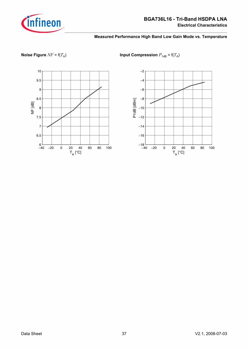
Data Sheet 37 V2.1, 2008-07-03
Noise Figure NF = f(TA) Input Compression P1dB = f(TA)
−40 −20 0 20 40 60 80 1006
6.5
7
7.5
8
8.5
9
9.5
10
TA [°C]
NF
[dB
]
−40 −20 0 20 40 60 80 100−18
−16
−14
−12
−10
−8
−6
−4
−2
TA [°C]
P1d
B [d
Bm
]

BGA736L16 - Tri-Band HSDPA LNAApplication Circuit and Block Diagram
UMTS bands I, II and V Application Circuit Schematic
Data Sheet 38 V2.1, 2008-07-03
3 Application Circuit and Block Diagram
3.1 UMTS bands I, II and V Application Circuit Schematic
Figure 2 Application circuit with chip outline (top view)
Note: Package paddle (Pin 0) has to be RF grounded.
Table 13 Parts ListPart Number Part Type Manufacturer Size CommentL1...L3 Chip inductor Various 0402 Wirewound, Q ≈ 50C1...C7 Chip capacitor Various 0402RREF Chip resistor Various 0402
BGA736L16_Appl_T_071210 .vsd
L13.9
C53.0pF
VCC = 2.8 V VGS = 0 / 2.8 V
RFOUT1900 MHz
RFIN800 MHz
VEN = 0 / 2.8 V VEN = 0 / 2.8 V
0 GND
C7100nF
8
7
6
9 10 11 12 13
14
15
16
12345
Biasing & LogicCircuitry
VCC VGS1
RFOUTM
RFOUTH
RFOUTL
VEN1VEN 2RFINL
RFINM
RFINH
n/c
n/c RFGNDH
RFGNDM
RREF8.2 kΩ
RREF
VGS2
VGS = 0 / 2.8 V
C639pF
L38.2nH
RFIN2100 MHz
RFIN1900 MHz
C139pF
C28.2pF
L14.7nH
C318pF
C422pF
L23.9nH
RFOUT2100 MHz
RFOUT800 MHz

Data Sheet 39 V2.1, 2008-07-03
BGA736L16 - Tri-Band HSDPA LNAApplication Circuit and Block Diagram
UMTS bands I, IV and VIII Application Circuit Schematic
3.2 UMTS bands I, IV and VIII Application Circuit Schematic
Figure 3 Application circuit with chip outline (top view)
Note: Package paddle (Pin 0) has to be RF grounded.
Table 14 Parts ListPart Number Part Type Manufacturer Size CommentL1...L5 Chip inductor Various 0402 Wirewound, Q ≈ 50C1...C7 Chip capacitor Various 0402RREF Chip resistor Various 0402
BGA736L16_Appl_Bands _IV_VIII.vsd
C118pF
L13. nH
VCC = 2.8 V VGS= 0 / 2.8 V
RFIN2100 MHz
VEN = 0 / 2.8 V VEN = 0 / 2.8 V
0 GND
8
7
6
9 10 11 12 13
14
15
16
12345
Biasing & LogicCircuitry
VCC VGS1
RFOUTM
RFOUTH
RFOUTL
VEN1VEN2RFINL
RFINM
RFINH
n/c
n/c RFGNDH
RFGNDM
RREF
VGS2
VGS = 0 / 2.8 V
C26.8pF
L13.4nH
RFIN2100 MHz
C318pF
C422pF
L23.9nH
RFOUT2100 MHz
RFOUT900 MHz
L53.9nH
RFOUT2100 MHz
L42.9nH
C53.0pF
RFIN900 MHz
C639pF
L37.3nH
C7100nF
RREF8.2kΩ

BGA736L16 - Tri-Band HSDPA LNAApplication Circuit and Block Diagram
Pin Definition
Data Sheet 40 V2.1, 2008-07-03
3.3 Pin Definition
Table 15 Pin Definition and FunctionPin Number Symbol Function0 GND Ground connection for low band (800/900 MHz) LNA and control
circuity (package paddle)1 VGS2 Gain step control2 VGS1 Gain step control3 VCC Supply voltage4 RFGNDH High band (2100 MHz) LNA RF ground5 n/c Not connected6 RFINM Mid band (1900/2100 MHz) LNA input7 RFINH High band (2100 MHz) LNA input8 RFGNDM Mid band (1900/2100 MHz) LNA RF ground9 n/c Not connected10 RFINL Low band (800/900 MHz) LNA input11 VEN2 Band select control12 VEN1 Band select control13 RREF Bias current reference resistor (high / mid gain mode)14 RFOUTL Low band (800/900 MHz) LNA output15 RFOUTH High band (2100 MHz) LNA output16 RFOUTM Mid band (1900/2100 MHz) LNA output

Data Sheet 41 V2.1, 2008-07-03
BGA736L16 - Tri-Band HSDPA LNAApplication Circuit and Block Diagram
Application Board
3.4 Application Board
Figure 4 Application board layout on 3-layer FR4. Top layer thickness: 0.2 mm, bottom layer thickness: 0.8 mm, 35 µm Cu metallization, gold plated. Board size: 20 x 50 mm
Figure 5 Cross-section view of application board

BGA736L16 - Tri-Band HSDPA LNAApplication Circuit and Block Diagram
Application Board
Data Sheet 42 V2.1, 2008-07-03
Figure 6 Detail of application board layout
Note: In order to achieve the same performance as given in this datasheet please follow the suggested PCB-layout as closely as possible. The position of the GND vias is critical for RF performance.

Data Sheet 43 V2.1, 2008-07-03
BGA736L16 - Tri-Band HSDPA LNAPhysical Characteristics
Package Footprint
4 Physical Characteristics
4.1 Package Footprint
Figure 7 Recommended footprint and stencil layout for the TSLP-16-1 package. SMD - V2 footprint is used on IFX application board
Stencil aperturesCopper Solder mask
NSMD
SMD - V1 SMD - V2 (e.g. BGA734L16)
0.225 0.225 0.2750.075
2.3
2.3
1.25
1.25
0.55
0.3 0.2 0.3 0.20.3 0.2 0.3
0.3 0.2
0.2250.35 0.55
2.3
0.3 0.2 0.3 0.20.3 0.2 0.3
0.3 0.2
0.3 0.2 0.3 0.20.3 0.2 0.3
0.3 0.2
1.25
0.15
0.2250.35 0.55
2.3
0.3 0.2 0.3 0.20.3 0.2 0.3
0.3 0.2
1.25
0.15
Copper Solder mask Vias top to first inner layerTSLP-16-1-FP V01

BGA736L16 - Tri-Band HSDPA LNA Physical Characteristics
Package Dimensions
Data Sheet 44 V2.1, 2008-07-03
4.2 Package Dimensions
Figure 8 Package outline (top, side and bottom view)
Top view Bottom view
Pin 1 marking
0.05 MAX.
0.39+0.01-0.03
16x0.2±0.0351
16
±0.0
51±0
.05
2
0.0
5x4
5˚ ±0.0
351
6x0
.21.4
±0.0
35
±0.0
52.
3
±0.0351.4
1±0.05
±0.052
±0.052.3
1)
1) Dimension applies to plated terminalsTSLP-16-1-PO V02
2345
15
14
13
9 1110 12
8
7
6
