bicmos current-controlled current feedback amplifier (cc ...msn/cccfa.pdf · bicmos...
TRANSCRIPT
BiCMOS Current-Controlled Current Feedback Amplifier (CC-CFA) and Its Applications
MONTREE SIRIPRUCHYANUN1, CHAIYAN CHANAPROMMA2, PHAMORN SILAPAN3 and
WINAI JAIKLA4 1,2 Department of Teacher Training in Electrical Engineering, Faculty of Technical Education, King
Mongkut’s University of Technology North Bangkok, Bangkok, 10800, THAILAND 3 Electric and Industrial Program, Faculty of Industrial Technology, Uttaradit Rajabhat University,
Muang, Uttaradit, 53000, THAILAND 4 Electric and Electronic Program, Faculty of Industrial Technology, Suan Sunandha Rajabhat
University, Dusit, Bangkok, 10300, THAILAND [email protected], [email protected], [email protected], [email protected]
http://www.te.kmutnb.ac.th/~msn/ Abstract: - This paper introduces a modified version of current feedback amplifier (CFA), called current controlled current feedback amplifier (CC-CFA), to extend usabilities of this active element in terms of electronic control-abilities and simpler circuit description of the element’s applications. This modified element was realized by using a BiCMOS standard technology to reduce offset error phenomenon, the design configuration is systematically explained. The performances have been proven through PSPICE which is accordance with theoretical anticipations. In addition, application examples for a current-mode multiplier/divider, oscillator, grounded inductance simulator, filters, and amplifiers are included. The results are confirmed that the electrical characteristics are electronically tunable. Key-Words: - CC-CFA, Current-mode, Voltage-mode, Filter, Oscillator, Inductance simulator, Multiplier 1 Introduction
There has been much effort to reduce the supply voltage of electronic circuits in the last decade. This is due to the demand for portable and battery-powered equipment. Since a low-voltage operating circuit becomes necessary, the current–mode technique is ideally suited for this purpose more than the voltage-mode one. Consequently, there is a growing interest in synthesizing the current-mode circuits because of more their potential advantages such as larger dynamic range, higher signal bandwidth, greater linearity, simpler circuitry and low power consumption [1-2]. Many active elements able to function in current-mode such as OTA, current feedback amplifier, current conveyor [3], current differencing buffered amplifier (CDBA) [4] and current differencing transconductance amplifier (CDTA) [5], and etc., have been introduced to response these demands.
Among the mentioned active building blocks, the current feedback amplifier (CFA) or current feedback operational amplifier (CFOA) is an interesting active component, especially suitable for a class of analog signal processing [6-8]. This device can operate in both current and voltage-modes, provides flexibility and enables a variety of
circuit designs. In addition, it can offer advantageous features such as high-slew rate, free from parasitic capacitances, wide bandwidth and simple implementation [9-11], Presently, the CFA can be commercially found, for example AD844 of Analog Devices Inc. [7]. It can be employed to realize filters [10-13], amplifiers [14], oscillators [15-19], inductance simulators [20-21], and etc. [22-24]. Conventionally, the electrical characteristics for applications of the CFAs cannot be adjusted by electronic methods, which this means that they cannot be controlled by currents and/or voltages. Although, they can be achieved by passive element adjustments, the electronic control method is being more popular more than those by passive elements (i.e. resistors and capacitors) [25] due to it can be easily adapted to automatic or microcontroller-based controls [26]. In addition, the CFA can not be controlled by the parasitic resistance at current input port so when it is used in a circuit, it must unavoidably require some external passive components, especially the resistors. This makes it not appropriate for IC implementation due to occupying more chip area, high power dissipation and cannot be electronic controllable. If it is employed for an off-the-shelf design, the circuit
WSEAS TRANSACTIONS on ELECTRONICSMontree Siripruchyanun, Chaiyan Chanapromma, Phamorn Silapan, Winai Jaikla
ISSN: 1109-9445 203 Issue 6, Volume 5, June 2008

description is composed of a large number of external passive elements. Actually, the electronic control can be done in a CFA application by replacing a resistor by junction field effect transistor (JFET) employed in voltage controlled resistor (VCR) region [19]. Unfortunately, it makes circuit description more complicated. Furthermore, the conventional CFA was designed by using the BJT and a basic voltage follower, consequently, this structure has problem for the output offset errors because the BJT current mirrors in the CFA provide errors due to practically internal factors more than a current mirror based on CMOS [27]. The offset output error from the basic voltage follower also affects the accuracies of circuits/systems. The offset problem is an important factor for circuit designers to be certain in practical implementations, especially in instrumentation and measurement systems.
In this work, thus, a modified-version CFA whose parasitic resistance at current input port can be controlled by an input bias current, called current controlled current feedback amplifier (CC-CFA), will be reviewed via this article. To reduce offset phenomenon, a BiCMOS technology is suitable for realizing the proposed element. In addition, the voltage follower is also developed to reduce the offset output current and voltage. The performances of proposed BiCMOS CC-CFA are illustrated by PSPICE simulations, they show good agreement as mentioned. The example applications as a multiplier/divider, oscillator, grounded inductance simulator, filters, and amplifiers are included. 2 Circuit Configuration 2.1 Basic Concept of CFA The CFA properties can be shown in the following equation
0 0 0 00 1 0 01 0 0 00 0 1 0
y x
yx
z z
w w
I IVV
I VV V
⎡ ⎤ ⎡ ⎤⎡ ⎤⎢ ⎥ ⎢ ⎥⎢ ⎥⎢ ⎥ ⎢ ⎥⎢ ⎥=⎢ ⎥ ⎢ ⎥⎢ ⎥⎢ ⎥ ⎢ ⎥⎢ ⎥⎢ ⎥ ⎢ ⎥⎣ ⎦⎣ ⎦ ⎣ ⎦
. (1)
The symbol and the equivalent circuit of the CFA are illustrated in Fig. 1(a) and (b), respectively. A circuit implementation of CFA can be achieved by using second-generation current conveyor (CCII) as input stage, followed by a buffered amplifier as depicted in Fig. 1(c).
zv
yv
xv
yi
xi
zi
wvy
x zwCFA
(a)
1 xi
1
zizv
xv
yv yi
xi wv
(b)
CCII zy
xxv
yv1 wv
zizv
yi
xi
(c)
Figure 1. CFA (a) Symbol (b) Equivalent circuit (c)
Element implementation 2.2 Basic Concept of CC-CFA CC-CFA properties are similar to the conventional CFA, except that the CC-CFA has finite input resistance Rx at the x input terminal. This parasitic resistance can be controlled by the bias current IB as shown in the following equation
0 0 0 01 0 0
1 0 0 00 0 1 0
y x
yxx
z z
w w
I IVRV
I VV V
⎡ ⎤ ⎡ ⎤⎡ ⎤⎢ ⎥ ⎢ ⎥⎢ ⎥⎢ ⎥ ⎢ ⎥⎢ ⎥=⎢ ⎥ ⎢ ⎥⎢ ⎥⎢ ⎥ ⎢ ⎥⎢ ⎥⎢ ⎥ ⎢ ⎥⎣ ⎦⎣ ⎦ ⎣ ⎦
, (2)
where
2T
xB
VR
I= . (3)
TV is the thermal voltage, which is 26mV at room
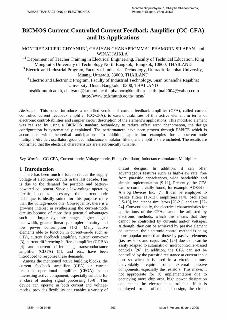
temperature. The symbol and equivalent circuit of the CC-CFA are illustrated in Fig. 2(a) and (b), respectively. In similar, we can realize the CC-CFA by using second-generation current controlled current conveyor (CCCII) as input stage, followed by a buffered amplifier as illustrated in Fig. 2(c).
WSEAS TRANSACTIONS on ELECTRONICSMontree Siripruchyanun, Chaiyan Chanapromma, Phamorn Silapan, Winai Jaikla
ISSN: 1109-9445 204 Issue 6, Volume 5, June 2008
zv
yv
xv
yi
xi
zi
wvy
x zw
BI
CC-CFA
(a)
1 xi
1
zizv
xv
yv yi
xi wv
(b)
CCCII zy
xxv
yv1 wv
zizv
yi
xi
(c)
Figure 2. CC-CFA (a) Symbol (b) Equivalent circuit
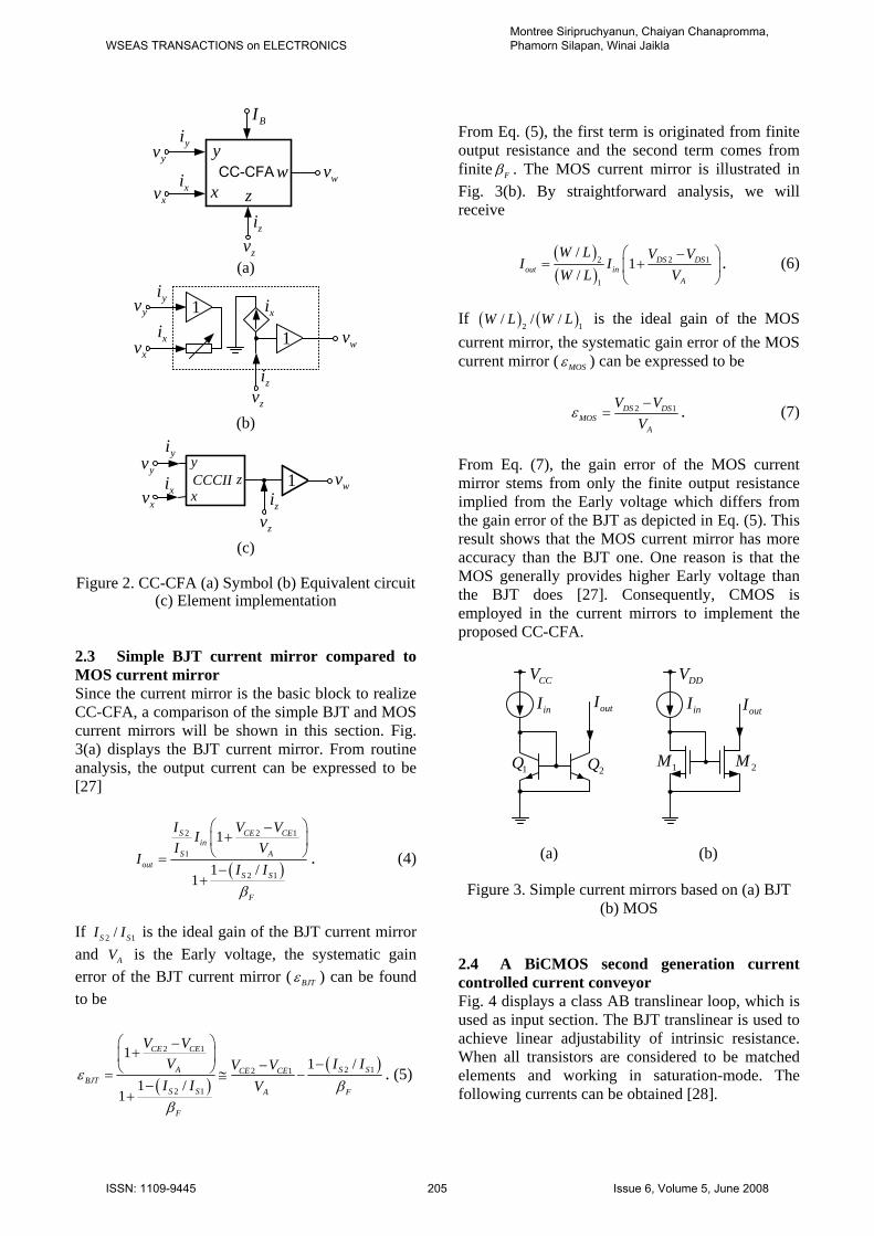
(c) Element implementation 2.3 Simple BJT current mirror compared to MOS current mirror Since the current mirror is the basic block to realize CC-CFA, a comparison of the simple BJT and MOS current mirrors will be shown in this section. Fig. 3(a) displays the BJT current mirror. From routine analysis, the output current can be expressed to be [27]
( )
2 2 1
1
2 1
1
1 /1
S CE CEin
S Aout
S S
F
I V VII V
II Iβ
⎛ ⎞−+⎜ ⎟
⎝ ⎠=−
+. (4)
If 2 1/S SI I is the ideal gain of the BJT current mirror and AV is the Early voltage, the systematic gain error of the BJT current mirror ( BJTε ) can be found to be
( )( )
2 1
2 12 1
2 1
11 /
1 /1
CE CE
A S SCE CEBJT
S S A F
F
V VV I IV V
I I Vε
ββ
⎛ ⎞−+⎜ ⎟ −−⎝ ⎠= ≅ −−
+. (5)
From Eq. (5), the first term is originated from finite output resistance and the second term comes from finite Fβ . The MOS current mirror is illustrated in Fig. 3(b). By straightforward analysis, we will receive
( )( )
2 12
1
/1
/DS DS
out inA
W L V VI I
W L V⎛ ⎞−
= +⎜ ⎟⎝ ⎠
. (6)
If ( ) ( )2 1
/ / /W L W L is the ideal gain of the MOS current mirror, the systematic gain error of the MOS current mirror ( MOSε ) can be expressed to be
2 1DS DSMOS
A
V VV
ε−
= . (7)
From Eq. (7), the gain error of the MOS current mirror stems from only the finite output resistance implied from the Early voltage which differs from the gain error of the BJT as depicted in Eq. (5). This result shows that the MOS current mirror has more accuracy than the BJT one. One reason is that the MOS generally provides higher Early voltage than the BJT does [27]. Consequently, CMOS is employed in the current mirrors to implement the proposed CC-CFA.
1M 2M
inI outIDDV
1Q 2Q
inICCV
outI
(a) (b)
Figure 3. Simple current mirrors based on (a) BJT (b) MOS
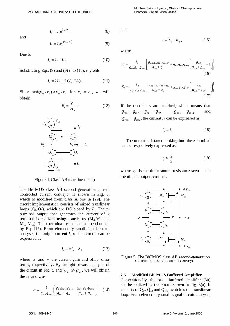
2.4 A BiCMOS second generation current controlled current conveyor Fig. 4 displays a class AB translinear loop, which is used as input section. The BJT translinear is used to achieve linear adjustability of intrinsic resistance. When all transistors are considered to be matched elements and working in saturation-mode. The following currents can be obtained [28].
WSEAS TRANSACTIONS on ELECTRONICSMontree Siripruchyanun, Chaiyan Chanapromma, Phamorn Silapan, Winai Jaikla
ISSN: 1109-9445 205 Issue 6, Volume 5, June 2008
( )/7
xy TV VBI I e= (8)
and ( )/
9xy TV V
BI I e−= . (9) Due to
7 9xI I I= − . (10) Substituting Eqs. (8) and (9) into (10), it yields
2 sinh( / )x B xy TI I V V= . (11) Since sinh( / ) /xy T xy TV V V V≅ for xy TV V , we will obtain
2T
xB
VR
I= . (12)
BI
BI
6Q 7Q
8Q 9Q
9I
7I
xIxV
CCV
EEV
yV
Figure 4. Class AB translinear loop The BiCMOS class AB second generation current controlled current conveyor is shown in Fig. 5, which is modified from class A one in [29]. The circuit implementation consists of mixed translinear loops (Q6-Q9), which are DC biased by IB. The z-terminal output that generates the current of x terminal is realized using transistors (M4-M5 and M12-M13). The x terminal resistance can be obtained by Eq. (12). From elementary small-signal circuit analysis, the output current IZ of this circuit can be expressed as
z xI Iα ε= + , (13) where α and ε are current gain and offset error terms, respectively. By straightforward analysis of the circuit in Fig. 5 and mi ig gπ , we will obtain the α and ε as
4 9 13 5 7 12
4 12 9 7 9 7
1 m m m m m m
m m m m m m
g g g g g gg g g g g g
α⎛ ⎞
= +⎜ ⎟+ +⎝ ⎠ (14)
and
1 2K Kε = + , (15) where
4 7 9 13 71 5 7 12
4 6 12 9 7 9 7
1m m m m mBm m m
m m m m m m m
g g g g gIK g g g
g g g g g g g⎡ ⎤⎛ ⎞
= + −⎢ ⎥⎜ ⎟+ +⎢ ⎥⎝ ⎠⎣ ⎦(16)
5 7 9 12 9
2 4 9 134 8 12 9 7 9 7
1m m m m mBm m m
m m m m m m m
g g g g gIK g g g
g g g g g g g⎡ ⎤⎛ ⎞
= + −⎢ ⎥⎜ ⎟+ +⎢ ⎥⎝ ⎠⎣ ⎦(17)
If the transistors are matched, which means that
6 7 8 9m m m mg g g g= = = , 12 13m mg g= and
4 5m mg g= , the current IZ can be expressed as
z xI I= . (18)
The output resistance looking into the z terminal can be respectively expressed as
2ds
zr
r ≅ , (19)
where dsr is the drain-source resistance seen at the mentioned output terminal.
6Q
7Q
8Q
9Q
4M
5M
12M
13M
x
BI
y z
DDV
SSV
BI
Figure 5. The BiCMOS class AB second-generation current controlled current conveyor
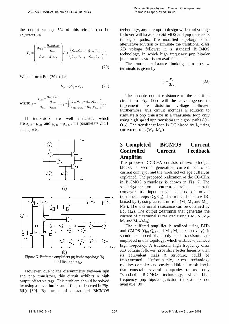
2.5 Modified BiCMOS Buffered Amplifier Conventionally, the basic buffered amplifier [30] can be realized by the circuit shown in Fig. 6(a). It consists of Q10-Q12 and Q14p, which is the translinear loop. From elementary small-signal circuit analysis,
WSEAS TRANSACTIONS on ELECTRONICSMontree Siripruchyanun, Chaiyan Chanapromma, Phamorn Silapan, Winai Jaikla
ISSN: 1109-9445 206 Issue 6, Volume 5, June 2008
the output voltage VW of this circuit can be expressed as
( )( )
11 1211
11 12 10 1210
11 14 10 14 11 12
.
m mm
m m m mmw z A
m m p m m p m m
g ggg g g gg
V V Ig g g g g g
⎛ ⎞+⎜ ⎟ −⎜ ⎟= ++⎜ ⎟ −
⎜ ⎟⎝ ⎠
(20) We can form Eq. (20) to be
w z bV Vγ ε= + , (21)
where 11 12
1110 11 12 10 12
11 14 10 14 11 12
,
m mm
m m m m mb A
m m p m m p m m
g ggg g g g g
Ig g g g g g
γ ε+ ⎛ ⎞−
= = ⎜ ⎟⎜ ⎟+ −⎝ ⎠.
If transistors are well matched, which
are 10 11m mg g= and 12 14m m pg g= , the parameters 1β ≅ and 0bε = .
(a)
(b) Figure 6. Buffered amplifiers (a) basic topology (b)
modified topology
However, due to the dissymmetry between npn and pnp transistors, this circuit exhibits a high output offset voltage. This problem should be solved by using a novel buffer amplifier, as depicted in Fig. 6(b) [30]. By means of a standard BiCMOS
technology, any attempt to design wideband voltage follower will have to avoid MOS and pnp transistors in signal paths. The modified topology is an alternative solution to simulate the traditional class AB voltage follower in a standard BiCMOS technology, in which high frequency pnp bipolar junction transistor is not available.
The output resistance looking into the w terminals is given by
2T
wA
Vr
I= . (22)
The tunable output resistance of the modified
circuit in Eq. (22) will be advantageous to implement low distortion voltage follower. Furthermore, this circuit includes a solution to simulate a pnp transistor in a translinear loop only using high speed npn transistors in signal paths (Q9-Q12). The translinear loop is DC biased by IA using current mirrors (M14-M21). 3 Completed BiCMOS Current Controlled Current Feedback Amplifier The proposed CC-CFA consists of two principal blocks: a second generation current controlled current conveyor and the modified voltage buffer, as explained. The proposed realization of the CC-CFA in BiCMOS technology is shown in Fig. 7. The second-generation current-controlled current conveyor as input stage consists of mixed translinear loops (Q6-Q9). The mixed loops are DC biased by IB using current mirrors (M1-M3 and M10-M11). The x terminal resistance can be obtained by Eq. (12). The output z-terminal that generates the current of x terminal is realized using CMOS (M4-M5 and M12-M13).
The buffered amplifier is realized using BJTs and CMOS (Q10-Q22 and M14-M21, respectively). It should be noted that only npn transistors are employed in this topology, which enables to achieve high frequency. A traditional high frequency class AB voltage follower, providing better linearity than its equivalent class A structure, could be implemented. Unfortunately, such technology requires complex and costly additional mask levels that constrain several companies to use only “standard” BiCMOS technology, which high frequency pnp bipolar junction transistor is not available [30].
WSEAS TRANSACTIONS on ELECTRONICSMontree Siripruchyanun, Chaiyan Chanapromma, Phamorn Silapan, Winai Jaikla
ISSN: 1109-9445 207 Issue 6, Volume 5, June 2008
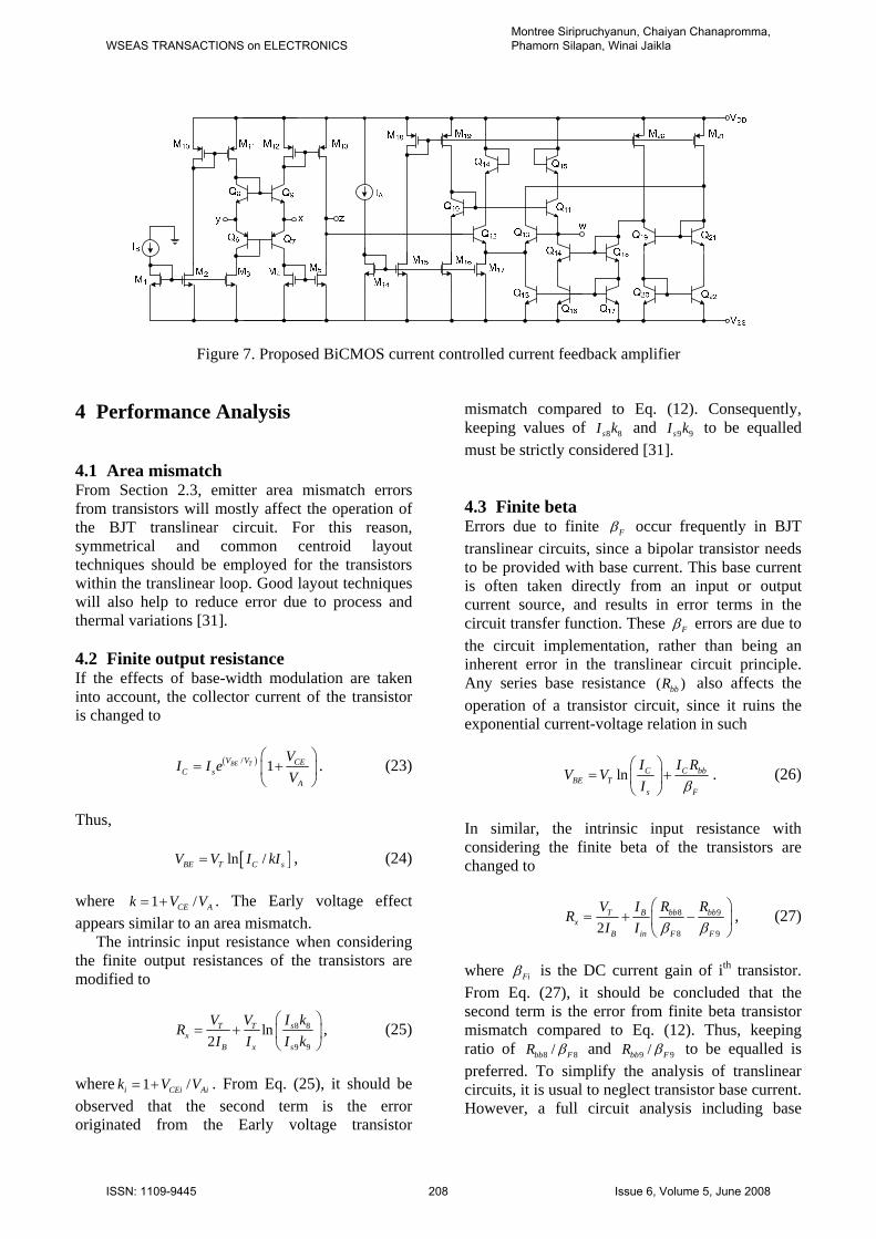
Figure 7. Proposed BiCMOS current controlled current feedback amplifier 4 Performance Analysis 4.1 Area mismatch From Section 2.3, emitter area mismatch errors from transistors will mostly affect the operation of the BJT translinear circuit. For this reason, symmetrical and common centroid layout techniques should be employed for the transistors within the translinear loop. Good layout techniques will also help to reduce error due to process and thermal variations [31]. 4.2 Finite output resistance If the effects of base-width modulation are taken into account, the collector current of the transistor is changed to
( )/ 1BE TV V CEC s
A
VI I e
V⎛ ⎞
= +⎜ ⎟⎝ ⎠
. (23)
Thus,
[ ]ln /BE T C sV V I kI= , (24) where 1 /CE Ak V V= + . The Early voltage effect appears similar to an area mismatch.
The intrinsic input resistance when considering the finite output resistances of the transistors are modified to
8 8
9 9
ln2
sT Tx
B x s
I kV VR
I I I k⎛ ⎞
= + ⎜ ⎟⎝ ⎠
, (25)
where 1 /i CEi Aik V V= + . From Eq. (25), it should be observed that the second term is the error originated from the Early voltage transistor
mismatch compared to Eq. (12). Consequently, keeping values of 8 8sI k and 9 9sI k to be equalled must be strictly considered [31]. 4.3 Finite beta Errors due to finite Fβ occur frequently in BJT translinear circuits, since a bipolar transistor needs to be provided with base current. This base current is often taken directly from an input or output current source, and results in error terms in the circuit transfer function. These Fβ errors are due to the circuit implementation, rather than being an inherent error in the translinear circuit principle. Any series base resistance ( )bbR also affects the operation of a transistor circuit, since it ruins the exponential current-voltage relation in such
ln C C bbBE T
s F
I I RV V
I β⎛ ⎞
= +⎜ ⎟⎝ ⎠
. (26)
In similar, the intrinsic input resistance with considering the finite beta of the transistors are changed to
8 9
8 92bb bbT B
xB in F F
R RV IR
I I β β⎛ ⎞
= + −⎜ ⎟⎝ ⎠
, (27)
where Fiβ is the DC current gain of ith transistor. From Eq. (27), it should be concluded that the second term is the error from finite beta transistor mismatch compared to Eq. (12). Thus, keeping ratio of 8 8/bb FR β and 9 9/bb FR β to be equalled is preferred. To simplify the analysis of translinear circuits, it is usual to neglect transistor base current. However, a full circuit analysis including base
WSEAS TRANSACTIONS on ELECTRONICSMontree Siripruchyanun, Chaiyan Chanapromma, Phamorn Silapan, Winai Jaikla
ISSN: 1109-9445 208 Issue 6, Volume 5, June 2008
current errors is often useful for comparing alternative circuit topologies [31].
TABLE I
Dimensions of the MOS transistors
MOS Transistors ( ) / ( )W m L mμ μM1, M3
M2 M4-M5, M18-M19
M10-M13 M14-M17, M20-M21
9/0.5 8.5/0.5 5/0.5
15/0.5 4/0.5
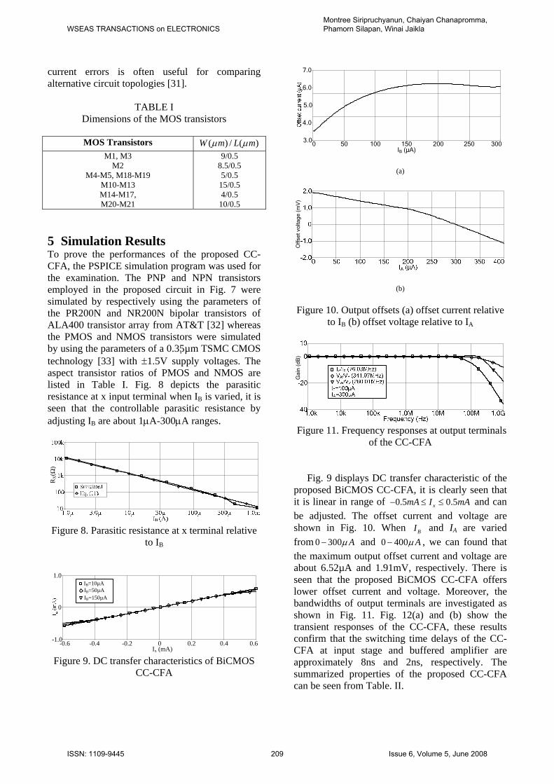
10/0.5 5 Simulation Results To prove the performances of the proposed CC-CFA, the PSPICE simulation program was used for the examination. The PNP and NPN transistors employed in the proposed circuit in Fig. 7 were simulated by respectively using the parameters of the PR200N and NR200N bipolar transistors of ALA400 transistor array from AT&T [32] whereas the PMOS and NMOS transistors were simulated by using the parameters of a 0.35 µm TSMC CMOS technology [33] with ±1.5V supply voltages. The aspect transistor ratios of PMOS and NMOS are listed in Table I. Fig. 8 depicts the parasitic resistance at x input terminal when IB is varied, it is seen that the controllable parasitic resistance by adjusting IB are about 1μA-300μA ranges.
RX(Ω
)
Figure 8. Parasitic resistance at x terminal relative to IB
Ix (mA)-0.6 -0.4 -0.2 0 0.2 0.4 0.6-1.0
0
1.0IB=10µAIB=50µAIB=150µA
Figure 9. DC transfer characteristics of BiCMOS
CC-CFA
IB (µA)0 50 100 150 200 250 300
3.0
4.0
5.0
6.0
7.0
(a)
Offs
et v
olta
ge (
mV
)
(b)
Figure 10. Output offsets (a) offset current relative to IB (b) offset voltage relative to IA
Gai
n (d
B)
Figure 11. Frequency responses at output terminals of the CC-CFA
Fig. 9 displays DC transfer characteristic of the
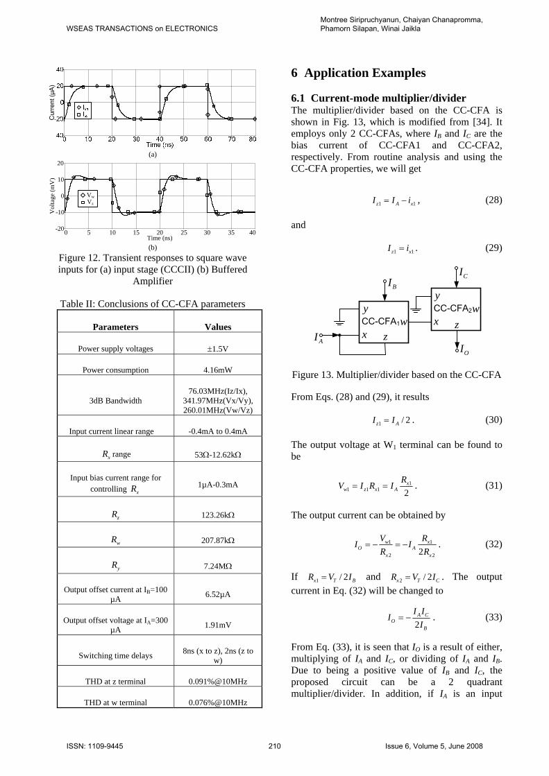
proposed BiCMOS CC-CFA, it is clearly seen that it is linear in range of 0.5 0.5xmA I mA− ≤ ≤ and can be adjusted. The offset current and voltage are shown in Fig. 10. When BI and IA are varied from 0 300 Aμ− and 0 400 Aμ− , we can found that the maximum output offset current and voltage are about 6.52µA and 1.91mV, respectively. There is seen that the proposed BiCMOS CC-CFA offers lower offset current and voltage. Moreover, the bandwidths of output terminals are investigated as shown in Fig. 11. Fig. 12(a) and (b) show the transient responses of the CC-CFA, these results confirm that the switching time delays of the CC-CFA at input stage and buffered amplifier are approximately 8ns and 2ns, respectively. The summarized properties of the proposed CC-CFA can be seen from Table. II.
WSEAS TRANSACTIONS on ELECTRONICSMontree Siripruchyanun, Chaiyan Chanapromma, Phamorn Silapan, Winai Jaikla
ISSN: 1109-9445 209 Issue 6, Volume 5, June 2008
Cur
rent
(µA
)
(a)
Time (ns)0 5 10 15 20 25 30 35 40-20
-10
0
10
20
Vol
tage
(mV
)
Vz
Vw
(b)
Figure 12. Transient responses to square wave inputs for (a) input stage (CCCII) (b) Buffered
Amplifier
Table II: Conclusions of CC-CFA parameters
Parameters Values
Power supply voltages ±1.5V
Power consumption 4.16mW
3dB Bandwidth 76.03MHz(Iz/Ix),
341.97MHz(Vx/Vy), 260.01MHz(Vw/Vz)
Input current linear range -0.4mA to 0.4mA
xR range 53Ω-12.62kΩ
Input bias current range for controlling xR 1µA-0.3mA
zR 123.26kΩ
wR 207.87kΩ
yR 7.24MΩ
Output offset current at IB=100 µA 6.52µA
Output offset voltage at IA=300 µA 1.91mV
Switching time delays 8ns (x to z), 2ns (z to w)
THD at z terminal 0.091%@10MHz
THD at w terminal 0.076%@10MHz
6 Application Examples 6.1 Current-mode multiplier/divider The multiplier/divider based on the CC-CFA is shown in Fig. 13, which is modified from [34]. It employs only 2 CC-CFAs, where IB and IC are the bias current of CC-CFA1 and CC-CFA2, respectively. From routine analysis and using the CC-CFA properties, we will get
1 1z A xI I i= − , (28)
and
1 1z xI i= . (29)
AI
y
x zw
BIy
x zw
CI
OI
CC-CFA1
CC-CFA2
Figure 13. Multiplier/divider based on the CC-CFA
From Eqs. (28) and (29), it results
1 / 2z AI I= . (30)
The output voltage at W1 terminal can be found to be
11 1 1 2
xw z x A
RV I R I= = . (31)
The output current can be obtained by
1 1
2 22w x
O Ax x
V RI I
R R= − = − . (32)
If 1 / 2x T BR V I= and 2 / 2x T CR V I= . The output current in Eq. (32) will be changed to
2A C
OB
I II
I= − . (33)
From Eq. (33), it is seen that IO is a result of either, multiplying of IA and IC, or dividing of IA and IB. Due to being a positive value of IB and IC, the proposed circuit can be a 2 quadrant multiplier/divider. In addition, if IA is an input
WSEAS TRANSACTIONS on ELECTRONICSMontree Siripruchyanun, Chaiyan Chanapromma, Phamorn Silapan, Winai Jaikla
ISSN: 1109-9445 210 Issue 6, Volume 5, June 2008
current, the proposed circuit can work as a current amplifier, while the magnitude of output current can be controlled by IB and IC. Furthermore, the output current is theoretically temperature-insensitive owing to no term of VT.
For non-ideal case, the xV , zI and wV of CC-CFA can be respectively characterized by
,x y x x z x zV V I R I Iβ α ε= + = + , (34) and
w z bV Vγ ε= + , (35) where α , β and γ are transferred error values deviated from one. zε and bε are the offset current and voltage at z, and w terminals, respectively. In the case of non-ideal and brief considerations, the IO is subsequently changed to
11 12 1 2 1 2
1 1 2
21 1
A C C b CzO z
B B T
I I I II
I I Vεα ε
α γ α γ εα α α
= + + ++ +
.(36)
From Eq. (36), we can see that the last three
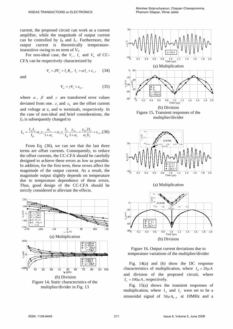
terms are offset currents. Consequently, to reduce the offset currents, the CC-CFA should be carefully designed to achieve these errors as low as possible. In addition, for the first term, these errors affect the magnitude of the output current. As a result, the magnitude output slightly depends on temperature due to temperature dependence of these errors. Thus, good design of the CC-CFA should be strictly considered to alleviate the effects.
I O(µ
A)
(a) Multiplication
I O(µ
A)
(b) Division Figure 14. Static characteristics of the
multiplier/divider in Fig. 13
Time (µs)0 0.2 0.4 0.6 0.8 1.0 1.2 1.4 1.6 1.8 2.0-50
0
50
IB=20µA
(a) Multiplication
Time (µs)0 0.2 0.4 0.6 0.8 1.0 1.2 1.4 1.6 1.8 2.0-80
-60
-40
-20
0
0
20
40
60
IO
IC=50µAIA=50µA
IB
(b) Division Figure 15. Transient responses of the
multiplier/divider
Time (µs)0 0.2 0.4 0.6 0.8 1.0 1.2 1.4 1.6 1.8 2.0-50
0
50Time (µs)
0.515 0.520 0.525 0.530 0.535 0.54030.0
32.5
35.0
27 C°50 C°100 C°
ZOOM
(a) Multiplication
Time (µs)0 0.2 0.4 0.6 0.8 1.0 1.2 1.4 1.6 1.8 2.0-80
-60
-40
-20
0
27 C°50 C°100 C°
Time (µs)0.97 0.99 1.01 1.03 1.05-72
-68
-64
-60
ZOOM
(b) Division
Figure 16. Output current deviations due to temperature variations of the multiplier/divider Fig. 14(a) and (b) show the DC response
characteristics of multiplication, where 20BI Aμ= and division of the proposed circuit, where
100CI Aμ= , respectively. Fig. 15(a) shows the transient responses of
multiplication, where AI and CI were set to be a sinusoidal signal of 50 P PAμ − at 10MHz and a
WSEAS TRANSACTIONS on ELECTRONICSMontree Siripruchyanun, Chaiyan Chanapromma, Phamorn Silapan, Winai Jaikla
ISSN: 1109-9445 211 Issue 6, Volume 5, June 2008
triangular signal 50 PAμ at 1MHz frequency, respectively. Fig. 15(b) shows the division of the proposed circuit, where AI and CI were set to be 50µA and BI was a triangular signal with a frequency of 1MHz. Furthermore, the claimed temperature-insensitivities of the proposed circuit are confirmed by the results of Fig. 16, depicting transient responses.
x
y zw
1BIx
y zw
2BI
OV
1C2C
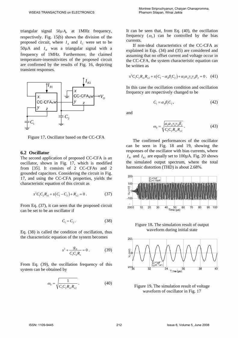
Figure 17. Oscillator based on the CC-CFA 6.2 Oscillator The second application of proposed CC-CFA is an oscillator, shown in Fig. 17, which is modified from [35]. It consists of 2 CC-CFAs and 2 grounded capacitors. Considering the circuit in Fig. 17, and using the CC-CFA properties, yields the characteristic equation of this circuit as
( )21 2 1 1 2 2 0x xs C C R s C C R+ − + = . (37)
From Eq. (37), it can seen that the proposed circuit can be set to be an oscillator if
1 2C C= . (38)
Eq. (38) is called the condition of oscillation, thus the characteristic equation of the system becomes
2
1 2
0m
x
gs
C C R+ = . (39)
From Eq. (39), the oscillation frequency of this system can be obtained by
01 2 1 2
1
x xC C R Rω = . (40)
It can be seen that, from Eq. (40), the oscillation frequency ( 0ω ) can be controlled by the bias currents.
If non-ideal characteristics of the CC-CFA as explained in Eqs. (34) and (35) are considered and assuming that no offset current and voltage occur in the CC-CFA, the system characteristic equation can be written as
( )2
1 2 1 2 1 1 1 2 1 2 1 2 2 0x xs C C R R s C Cα β α α γ γ β+ − + = . (41) In this case the oscillation condition and oscillation frequency are respectively changed to be
1 1 1 2C Cα β= , (42) and
1 2 1 2 20
1 2 1 2x xC C R Rα α γ γ β
ω = . (43)
The confirmed performances of the oscillator
can be seen in Fig. 18 and 19, showing the responses of the oscillator with bias currents, where
1BI and 2BI are equally set to 100µA. Fig. 20 shows the simulated output spectrum, where the total harmonic distortion (THD) is about 2.68%.
Time (µs)0 10 20 30 40 50 60 70 80 90 100
-200
-100
0
100
200C1=1nFC2=1.15nF
Figure 18. The simulation result of output waveform during initial state
VO
(mV
)
Figure 19. The simulation result of voltage waveform of oscillator in Fig. 17
WSEAS TRANSACTIONS on ELECTRONICSMontree Siripruchyanun, Chaiyan Chanapromma, Phamorn Silapan, Winai Jaikla
ISSN: 1109-9445 212 Issue 6, Volume 5, June 2008
Frequency (Hz)0 0.5M 1.0M 1.5M 2.0M 2.5M 3.0M 3.5M 4.0M0
40
80
120
C1=1nFC2=1.15nFf0=820kHzTHD=2.68%
VO
(mV
)
Figure 20. The simulation result of output spectrum
y
xw
1BIy
x zw
2BI
C
inVinI
z
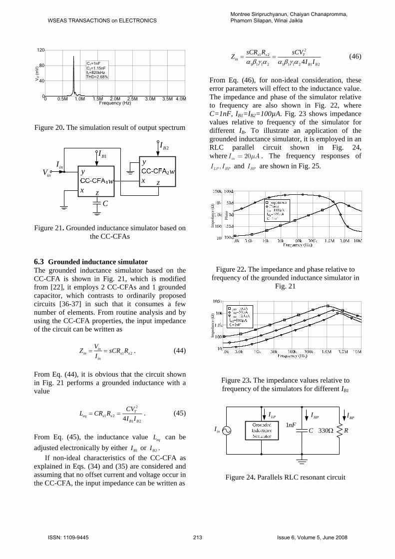
Figure 21. Grounded inductance simulator based on the CC-CFAs
6.3 Grounded inductance simulator The grounded inductance simulator based on the CC-CFA is shown in Fig. 21, which is modified from [22], it employs 2 CC-CFAs and 1 grounded capacitor, which contrasts to ordinarily proposed circuits [36-37] in such that it consumes a few number of elements. From routine analysis and by using the CC-CFA properties, the input impedance of the circuit can be written as
1 2in
in x xin
VZ sCR R
I= = . (44)
From Eq. (44), it is obvious that the circuit shown in Fig. 21 performs a grounded inductance with a value
2
1 21 24
Teq x x
B B
CVL CR R
I I= = . (45)
From Eq. (45), the inductance value eqL can be adjusted electronically by either 1BI or 2BI .
If non-ideal characteristics of the CC-CFA as explained in Eqs. (34) and (35) are considered and assuming that no offset current and voltage occur in the CC-CFA, the input impedance can be written as
21 2
1 1 1 2 1 1 1 2 1 24x x T
inB B
sCR R sCVZ
I Iα β γ α α β γ α= = (46)
From Eq. (46), for non-ideal consideration, these error parameters will effect to the inductance value. The impedance and phase of the simulator relative to frequency are also shown in Fig. 22, where C=1nF, IB1=IB2=100µA. Fig. 23 shows impedance values relative to frequency of the simulator for different IB. To illustrate an application of the grounded inductance simulator, it is employed in an RLC parallel circuit shown in Fig. 24, where 20inI Aμ= . The frequency responses of
,LP HPI I and BPI are shown in Fig. 25.
Impe
danc
e (Ω
)
Phas
e
Figure 22. The impedance and phase relative to frequency of the grounded inductance simulator in
Fig. 21
Impe
danc
e (Ω
)
Figure 23. The impedance values relative to frequency of the simulators for different IB1
LPI HPI BPI
330Ω1nF
C RinI
Figure 24. Parallels RLC resonant circuit
WSEAS TRANSACTIONS on ELECTRONICSMontree Siripruchyanun, Chaiyan Chanapromma, Phamorn Silapan, Winai Jaikla
ISSN: 1109-9445 213 Issue 6, Volume 5, June 2008
Gai
n (d
B)
Figure 25. Simulated current characteristics of the resonant circuit in Fig. 24
x
yw
1BIx
y zw
2BI
2C
1inV OV
2inV
3inV1C
CC-CFA1
CC-CFA2
z
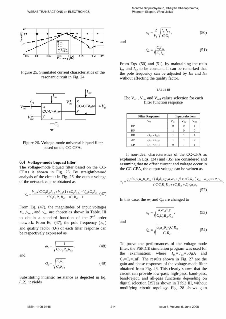
Figure 26. Voltage-mode universal biquad filter based on the CC-CFAs
6.4 Voltage-mode biquad filter The voltage-mode biquad filter based on the CC-CFAs is shown in Fig. 26. By straightforward analysis of the circuit in Fig. 26, the output voltage of the network can be obtained as
( )21 1 2 1 2 2 2 2 3 2 1
21 2 1 2 2 2
1.
1in x x in x in x
Ox x x
V s C C R R V sC R V sC RV
s C C R R sC R+ + −
=+ +
(47)
From Eq. (47), the magnitudes of input voltages
1 2,in inV V , and 3inV are chosen as shown in Table. III to obtain a standard function of the 2nd order network. From Eq. (47), the pole frequency ( 0ω ) and quality factor (Q0) of each filter response can be respectively expressed as
01 2 1 2
1
x xC C R Rω = , (48)
and 1 1
02 2
.x
x
C RQ
C R= (49)
Substituting intrinsic resistance as depicted in Eq. (12), it yields
1 20
1 2
2 ,B B
T
I IV C C
ω = (50)
and 1 2
02 1
.B
B
C IQ
C I= (51)
From Eqs. (50) and (51), by maintaining the ratio IB1 and IB2 to be constant, it can be remarked that the pole frequency can be adjusted by IB1 and IB2 without affecting the quality factor.
TABLE III
The Vin1, Vin2 and Vin3 values selection for each filter function response
Filter Responses Input selections
VO Vin1 Vin2 Vin3 BP 0 0 1 HP 1 0 0 BR (RX1=RX2) 1 1 1 AP (RX1=RX2) 1 1 2 LP (RX1=RX2) 0 1 1
If non-ideal characteristics of the CC-CFA as
explained in Eqs. (34) and (35) are considered and assuming that no offset current and voltage occur in the CC-CFA, the output voltage can be written as
( )22 1 2 1 2 1 2 2 2 1 1 3
21 2 1 2 2 2 2 1 1 2
1 2 1 2 1 2 1 2 2 2 .x x in in x inO
x x x
xV
s C C R R V V sC R V
s C C R R sC R
sC Rγ α γ
β γ α α
β β γ γ α α β γ −=
+ +
+ +
(52) In this case, the ω0 and Q0 are changed to
1 2 2 10
1 2 1 2
,x xC C R R
α α β γω = (53)
and 1 2 2 1 1 1
02 2
.x
x
C RQ
C Rα α β γ
= (54)
To prove the performances of the voltage-mode filter, the PSPICE simulation program was used for the examination, where 1BI = 2BI =50µA and C1=C2=1nF. The results shown in Fig. 27 are the gain and phase responses of the voltage-mode filter obtained from Fig. 26. This clearly shows that the circuit can provide low-pass, high-pass, band-pass, band-reject, and all-pass functions depending on digital selection [35] as shown in Table III, without modifying circuit topology. Fig. 28 shows gain
WSEAS TRANSACTIONS on ELECTRONICSMontree Siripruchyanun, Chaiyan Chanapromma, Phamorn Silapan, Winai Jaikla
ISSN: 1109-9445 214 Issue 6, Volume 5, June 2008
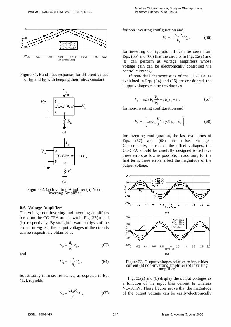
responses of band-pass function where IB1 and IB2 are equally set to keep the ratio to be constant and changed for several values. It is found that pole frequency can be adjusted without affecting the quality factor, as earlier explained.
Frequency (Hz)10k 30k 100k 300k 1.0M 3.0M 10M 30M-200d
-100d
0d
-60
-40
-20
010
Phas
e
Gai
n (d
B)
GainPhase
(a)
Frequency (Hz)10k 30k 100k 300k 1.0M 3.0M 10M 30M0d
90d
180d
-80
-40
0
40
Phas
e
Gai
n (d
B)
GainPhase
(b)
Gai
n (d
B)
Pha
se
(c)
Gai
n (d
B)
Phas
e
(d)
Frequency (Hz)10k 30k 100k 300k 1.0M 3.0M 10M 30M-400d
-200d
0d
-10
-5
0
5
10
GainPhase
(e)
Figure 27. Gain and phase responses of the voltage-mode biquad filter in Fig. 24 for different responses
(a) LP (b) HP (c) BP (d) BR (e) AP
Gai
n (d
B)
Figure 28. Band-pass responses for different values of IB1 and IB2 with keeping their ratios constant
x
y1z
w
1BI
y
x zw
2BI
2C
2z
1inI
2inI3inI
OI
1C
Figure 29. Current-mode universal biquad filter based on the CC-CFA
6.5 Current-mode biquad filter The fifth application of the proposed CC-CFA is a current-mode biquad filter shown in Fig. 29. It employs only 2 active elements and 2 grounded capacitors, which is easy to fabricate, unlike the previous circuits [38-39]. The CC-CFA in Fig. 29 is slightly modified from the proposed CC-CFA in Fig. 7 by using multiple-output CC-CFA which can be achieved by using the current mirrors to copy current from the z1 to the z2 terminal to extend the usability of CC-CFA. Straightforward analysis of the circuit in Fig. 29 and using CC-CFA properties in section 2, the output current of the network can be obtained as
( )21 2 2 2 3 1 2 1 2 2 2
21 2 1 2 2 2
1.
1in x in in x x x
Ox x x
I sC R I I s C C R R sC RI
s C C R R sC R
+ − + +=
+ +(55)
TABLE IV
The Iin1, Iin2 and Iin3 value selections for each filter function response
Filter Responses Input selections IO Iin1 Iin2 Iin3 BP 1 0 0 HP 1 1 1 BR 1 0 1 AP 2 0 1 LP 0 1 0
WSEAS TRANSACTIONS on ELECTRONICSMontree Siripruchyanun, Chaiyan Chanapromma, Phamorn Silapan, Winai Jaikla
ISSN: 1109-9445 215 Issue 6, Volume 5, June 2008
From Eq. (55), the magnitudes of input currents
1 2,in inI I , and 3inI can be chosen as in Table. IV to obtain a standard function of the 2nd order network. The circuit for selection can be seen in [40]. Moreover, Iin1 must be double of Iin3 in the case of AP. So to achieve this condition, the current amplifier which has gain of 2 is required. From Eq. (55), the pole frequency ( 0ω ) and quality factor (Q0) of each filter response can be respectively expressed as
01 2 1 2
1
x xC C R Rω = , (56)
and 1 1
02 2
.x
x
C RQ
C R= (57)
Substituting intrinsic resistance as depicted in Eq. (12), it yields
1 20
1 2
2 ,B B
T
I IV C C
ω = (58)
and 1 2
02 1
.B
B
C IQ
C I= (59)
If non-ideal characteristics of the CC-CFA as
explained in Eqs. (34) and (35) are considered and assuming that no offset current and voltage occur in the CC-CFA, the output current in Fig. 29 can be written as
1 2 2 12 2 2 2 1 12 3 ( )( )
in x in inO
I sC R I I D sI
D sα α β γ α+ −
= , (60)
where 21 2 1 2 2 2 2 1 11 12 2( ) x x xD s s C C R R sC R β γ α α α= + + .
In this case, the ω0 and Q0 are changed to
2 1 11 12 20
1 2 1 2
,x xC C R R
β γ α α αω = (61)
and 2 1 11 12 2 1 1
02 2
.x
x
C RQ
C Rβ γ α α α
= (62)
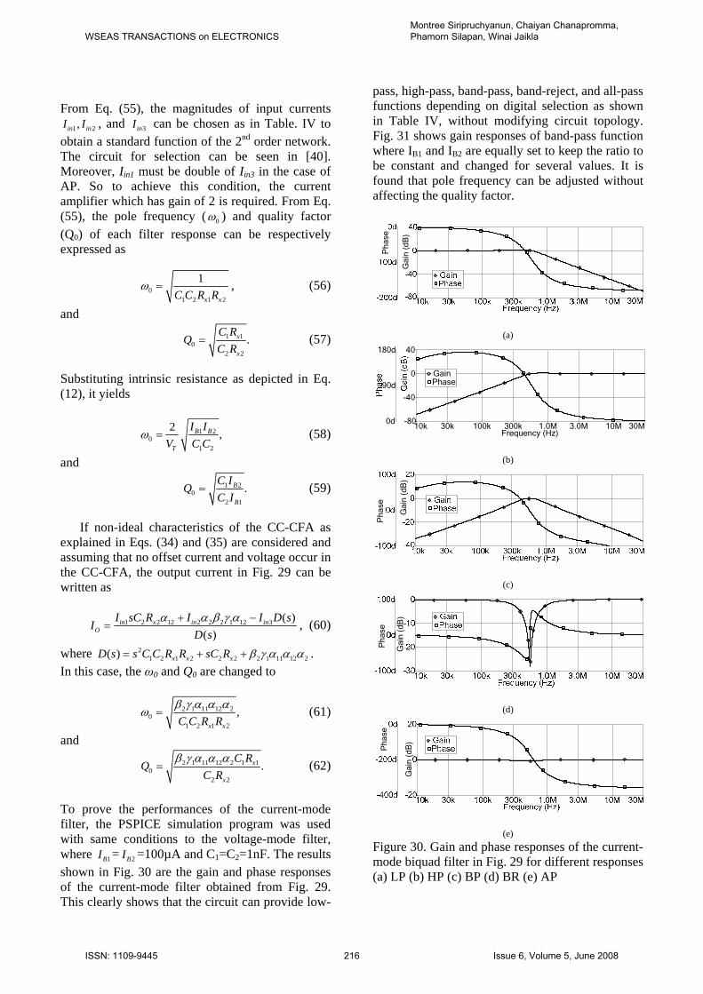
To prove the performances of the current-mode filter, the PSPICE simulation program was used with same conditions to the voltage-mode filter, where 1BI = 2BI =100µA and C1=C2=1nF. The results shown in Fig. 30 are the gain and phase responses of the current-mode filter obtained from Fig. 29. This clearly shows that the circuit can provide low-
pass, high-pass, band-pass, band-reject, and all-pass functions depending on digital selection as shown in Table IV, without modifying circuit topology. Fig. 31 shows gain responses of band-pass function where IB1 and IB2 are equally set to keep the ratio to be constant and changed for several values. It is found that pole frequency can be adjusted without affecting the quality factor.
Gai
n (d
B)
Pha
se
(a)
Frequency (Hz)10k 30k 100k 300k 1.0M 3.0M 10M 30M
0d
90d
180d
-80
-40
0
40
GainPhase
(b)
Gai
n (d
B)
Pha
se
(c)
Pha
se
Gai
n (d
B)
(d)
Gai
n (d
B)
Pha
se
(e)
Figure 30. Gain and phase responses of the current-mode biquad filter in Fig. 29 for different responses (a) LP (b) HP (c) BP (d) BR (e) AP
WSEAS TRANSACTIONS on ELECTRONICSMontree Siripruchyanun, Chaiyan Chanapromma, Phamorn Silapan, Winai Jaikla
ISSN: 1109-9445 216 Issue 6, Volume 5, June 2008
Frequency (Hz)10k 30k 100k 300k 1.0M 3.0M 10M 30M-60
-40
-20
0
IB1=IB2=25µAIB1=IB2=50µAIB1=IB2=100µA
Figure 31. Band-pass responses for different values of IB1 and IB2 with keeping their ratios constant
y
x zw
BI
inVOV
LR
CC-CFA
(a)
x
y zw
BI
inVOV
LR
CC-CFA
(b)
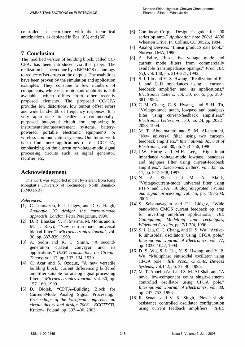
Figure 32. (a) Inverting Amplifier (b) Non-Inverting Amplifier
6.6 Voltage Amplifiers The voltage non-inverting and inverting amplifiers based on the CC-CFA are shown in Fig. 32(a) and (b), respectively. By straightforward analysis of the circuit in Fig. 32, the output voltages of the circuits can be respectively obtained as
,LO in
x
RV V
R= (63)
and L
O inx
RV V
R= − . (64)
Substituting intrinsic resistance, as depicted in Eq. (12), it yields
2,B L
O inT
I RV V
V= (65)
for non-inverting configuration and 2 B L
O inT
I RV V
V= − , (66)
for inverting configuration. It can be seen from Eqs. (65) and (66) that the circuits in Fig. 32(a) and (b) can perform as voltage amplifiers whose voltage gain can be electronically controlled via control current IB.
If non-ideal characteristics of the CC-CFA as explained in Eqs. (34) and (35) are considered, the output voltages can be rewritten as
,inO L L z b
x
VV R R
Rαβγ γ ε ε= + + (67)
for non-inverting configuration and
inO L L z b
x
VV R R
Rαγ γ ε ε⎛ ⎞
= − + +⎜ ⎟⎝ ⎠
, (68)
for inverting configuration, the last two terms of Eqs. (67) and (68) are offset voltages. Consequently, to reduce the offset voltages, the CC-CFA should be carefully designed to achieve these errors as low as possible. In addition, for the first term, these errors affect the magnitude of the output voltage.
VO
(mV
)
(a)
Time (µs)0 0.2 0.4 0.6 0.8 1.0 1.2 1.4 1.6 1.8 2.0-200
-100
0
100
200IB=100µAIB=150µAIB=200µA
RL=1kΩ
VO
(mV
) Iin
(b)
Figure 33. Output voltages relative to input bias current (a) non-inverting amplifier (b) inverting
amplifier
Fig. 33(a) and (b) display the output voltages as a function of the input bias current IB whereas Vin=10mV. These figures prove that the magnitude of the output voltage can be easily/electronically
WSEAS TRANSACTIONS on ELECTRONICSMontree Siripruchyanun, Chaiyan Chanapromma, Phamorn Silapan, Winai Jaikla
ISSN: 1109-9445 217 Issue 6, Volume 5, June 2008
controlled in accordance with the theoretical anticipations, as depicted in Eqs. (65) and (66). 7 Conclusion The modified version of building block, called CC-CFA, has been introduced via this paper. The realization has been done by a BiCMOS technology to reduce offset errors at the outputs. The usabilities have been proven by the simulation and application examples. They consume a few numbers of components, while electronic controllability is still available, which differs from other recently proposed elements. The proposed CC-CFA provides low distortions, low output offset errors and wide bandwidth of frequency responses. It is very appropriate to realize in commercially-purposed integrated circuit for employing in instrumentation/measurement systems, battery-powered, portable electronic equipments or wireless communication systems. Our future work is to find more applications of the CC-CFA, emphasizing on the current or voltage-mode signal processing circuits such as signal generator, rectifier, etc.
Acknowledgement
This work was supported in part by a grant from King Mongkut’s University of Technology North Bangkok (KMUTNB). References: [1] C. Toumazou, F. J. Lidgey, and D. G. Haigh,
Analogue IC design: the current-mode approach, London: Peter Peregrinus, 1990.
[2] D. R. Bhaskar, V. K. Sharma, M. Monis and S. M. I. Rizvi, “New curren-mode universal biquad filter,” Microelectronics Journal, vol. 30, pp. 837-839, 1999.
[3] A. Sedra and K. C. Smith, “A second-generation current conveyor and its applications,” IEEE Transactions on Circuits Theory, vol. 17, pp. 132–134, 1970
[4] C. Acar and S. Ozoguz, “A new versatile building block: current differencing buffered amplifier suitable for analog signal processing filters,” Microelectronics Journal, vol. 30, pp. 157–160, 1999.
[5] D. Biolek, “CDTA–Building Block for Current-Mode Analog Signal Processing,” Proceedings of the European conference on circuit theory and design 2003 - ECCTD'03, Krakow, Poland, pp. 397–400, 2003.
[6] Comlinear Corp., “Designer’s guide for 200 series op amp,” Application note 200-1, 4800 Wheaton Drive, Ft. Collins, CO 80525, 1984.
[7] Analog Devices: “Linear products data book.” Norwood MA, 1990.
[8] A. Fabre, “Insensitive voltage mode and current mode filters from commercially available transimpedance opamps,” Proc. IEE (G), vol. 140, pp. 319–321, 1993.
[9] S.-I. Liu and Y.-S. Hwang, “Realization of R–L and C–D impedances using a current-feedback amplifier and its applications,” Electronics Letters, vol. 30, no. 5, pp. 380–381, 1994.
[10] C.-M. Chang, C.-S. Hwang, and S.-H. Tu, “Voltage-mode notch, lowpass and bandpass filter using current-feedback amplifiers,” Electronics Letters, vol. 30, no. 24, pp. 2022–2023, 1994.
[11] M. T. Abuelma’atti and S. M. Al-shahrani, “New universal filter using two current-feedback amplifiers,” International Journal of Electronics, vol. 80, pp. 753–756, 1996.
[12] J-W. Horng and M-H. Lee,, “High input impedance voltage-mode lowpass, bandpass and highpass filter using current-feedback amplifiers,”. Electronics Letters, vol. 33, no. 11, pp. 947–948, 1997.
[13] N. A. Shah nad M. A. Malik, “Voltage/current-mode universal filter using FTFN and CFA,” Analog integrated circuits and signal processing, vol. 45, pp. 197-203, 2005.
[14] S. Selvanayagam and F.J. Lidgey, “Wide bandwidth CMOS current feedback op amp for inverting amplifier applications,” IEE Colloquium, Modelling and Techniques, Wideband Circuits, pp. 7/1-7/4, 1996.
[15] S. I. Liu, C. C. Chang, and D. S. Wu, “Active-R sinusoidal oscillators using CFOA pole,” International Journal of Electronics, vol. 77, pp. 1035–1042, 1994.
[16] D. S. Wu, S. I. Liu, Y. S. Hwang, and Y. P. Wu, “Multiphase sinusoidal oscillator using CFOA pole,” IEE Proc., Circuits, Devices Systems, vol.142, pp. 37–40, 1995.
[17] M. T. Abuelma’atti and S. M. Al-Shahrani, “A novel low-component count single-element-controlled oscillator using CFOA pole,” International Journal of Electronics, vol. 80, pp. 747–753, 1996.
[18] R. Senani and V. K. Singh, “Novel single resistance controlled oscillator configuration using current feedback amplifiers,” IEEE
WSEAS TRANSACTIONS on ELECTRONICSMontree Siripruchyanun, Chaiyan Chanapromma, Phamorn Silapan, Winai Jaikla
ISSN: 1109-9445 218 Issue 6, Volume 5, June 2008
Trans. Circuits Syst. I, vol. 43, pp. 698–700, 1996.
[19] S. S. Gupta, D. R. Bhaskar, R. Senani, “New voltage controlled oscillators using CFOAs,” International Journal of Electronics and Communications, available online, 2008.
[20] S. Natarajan, “Inductance simulation using modern current feedback amplifiers (CFAs),” Proceedings of the Thirty-Seventh Southeastern Symposium on System Theory, 2005, SSST'05,, pp. 60-64, 2005.
[21] T. K. Bandyopadhyay, R. K. Nagaria,S. K. Sanyal and R. Nandi, “Lossless inductor using current feedback amplifier,” International Symposium on Signals, Circuits and Systems, 2005. ISSCS 2005, vol. 2, pp. 689-692, 2005.
[22] A. Fabre, “Gyrator implementation from commercially available transimpedance operational amplifiers,” Electronics Letters, vol. 28, pp. 263-264, 1992.
[23] M. Abuelma'atti and S. al-Shahrani, “New CFOA-based triangular/square wave generator,” International Journal of Electronics, vol. 84, pp. 583–588, 1998.
[24] M. Weng, J. R Lai and M. H. Lee, “Realization of. nth-order series impedance function using only (n-1). current-feedback amplifiers,”. International Journal of Electronics, vol. 87, no. 1, p. 63-69, 2000.
[25] H. Z. Abouda and A. Fabre, “New high-value floating controlled resistor in CMOS technology,” IEEE Transaction on Instrumentation and Measurement, vol. 51, no. 7, pp.1017-1020, 2006.
[26] M. Siripruchyanun and W. Jaikla, “Electronically Controllable Current-Mode Universal Biquad Filter Using Single DO-CCCDTA,” Circuits Systems and Signal Processing, vol. 27, pp. 113-122, 2008.
[27] P. R. Gray, P. J. Hurst S. H. Lewis and R. G. Meyer, Analysis and Design of Analog Integrated Circuits, New York: John Wiley & Sons, 2001.
[28] A. Fabre, “Dual translinear voltage/current convertor,” Electronics Letters, vol. 19, pp. 1030-1031, 1983.
[29] F. Seguin and A. Fabre, “2 GHz controlled current conveyor in standard 0.8μm BICMOS technology,” Electronics Letters, vol. 37, pp. 329-330, 2001.
[30] H. Barthélemy and E. Kussener, “High speed voltage follower for standard BiCMOS technology,” IEEE Transaction on Circuits and Systems, vol. 48, pp. 727-732, 2001.
[31] A. Grebene, Bipolar and MOS analog integrated circuit design, John Wiley & Sons, Inc., New York, 1984.
[32] D. R. Frey “Log-domain filtering: an approach to current-mode filtering,” IEE Proc. Circuit Devices Syst., vol. 140. pp. 406-416, 1993.
[33] E. Yuce, S. Tokat, A. Kızılkaya and O. Cicekoglu, “CCII-based PID controllers employing grounded passive components,” International Journal of Electronics and Communication, vol. 60, no. 5, pp. 399-403, 2006.
[34] M. T. Abuelma’atti and M.A. Al Qahtani, “A current mode current controlled current conveyor based analogue multiplier/divider,” International Journal of Electronics, vol. 85, pp. 71-77, 1998.
[35] D. R. Bhaskar and Raj Senani, “New CFOA-Based single-element-controlled sinusoidal oscillators,” IEEE Transaction on Instrument and Measurement, vol. 55, pp. 2004-2221, 2006.
[36] I. A. Khan and M. H. Zaidi, “A novel ideal floating inductor using translinear conveyors,” Active and Passive Electronic Components, vol. 26, no. 2, pp. 87–89, 2003.
[37] J. S. Pena-Finol and J. A. Connelly, “Novel lossless floating immittance simulator employing only two FTFNs,” Analog Integrated Circuits and Signal Processing, vol. 29, no. 3, pp. 233-235, 2001.
[38] W. Tangsrirat, “Low-voltage digitally programmable current-mode universal biquadratic filter,” International Journal of Electronics and Communication, vol. 62, pp. 97-103, 2008.
[39] M. A. Ibrahim, S. Minaei, and H. A. Kuntman “A 22.5 MHz current-mode KHN-biquad using differential voltage current conveyor and grounded passive elements,” International Journal of Electronics and Communication, vol. 59, pp. 311-318, 2005.
[40] C. L. Hou, C. C. Huang, Y. S. Lan, J. J. Shaw and C. M. Chang “Current-mode and voltage-mode universal biquads using a single current-feedback amplifier,” International Journal of Electronics, vol. 86, no. 8, pp. 929-932, 1999.
WSEAS TRANSACTIONS on ELECTRONICSMontree Siripruchyanun, Chaiyan Chanapromma, Phamorn Silapan, Winai Jaikla
ISSN: 1109-9445 219 Issue 6, Volume 5, June 2008