bit error rate tester (bert) - maxim integrated - analog ... · and analyzer capable of meeting the...
TRANSCRIPT

1 of 23 101000
FEATURES� Generates/Detects digital bit patterns for
analyzing, evaluating and troubleshootingdigital communications systems
� Operates at speeds from DC to 52 MHz� Programmable polynomial length and
feedback taps for generation of any otherpseudorandom pattern up to 32 bits in lengthincluding: 26-1, 29-1, 211-1, 215-1, 220-1, 223-1,and 232-1
� Programmable user-defined pattern andlength for generation of any repetitive patternup to 32 bits in length
� Large 32-bit error count and bit countregisters
� Software programmable bit error insertion� Fully independent transmit and receive
sections� 8-bit parallel control port� Detects test patterns with bit error rates up to
10-2
PIN ASSIGNMENT
ORDERING INFORMATION DS2172T (00 C to 700 C) DS2172TN (-400 C to + 850 C)
DESCRIPTIONThe DS2172 Bit Error Rate Tester (BERT) is a software programmable test pattern generator, receiver,and analyzer capable of meeting the most stringent error performance requirements of digitaltransmission facilities. Two categories of test pattern generation (Pseudo-random and Repetitive)conform to CCITT/ITU O.151, O.152, O.153, and O.161 standards. The DS2172 operates at clock ratesranging from DC to 52 MHz. This wide range of operating frequency allows the DS2172 to be used inexisting and future test equipment, transmission facilities, switching equipment, multiplexers, DACs,Routers, Bridges, CSUs, DSUs, and CPE equipment.
The DS2172 user-programmable pattern registers provide the unique ability to generate loopback patternsrequired for T1, Fractional-T1, Smart Jack, and other test procedures. Hence the DS2172 can initiate theloopback, run the test, check for errors, and finally deactivate the loopback.
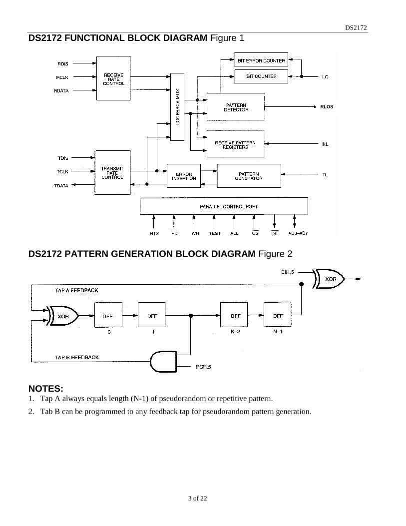
The DS2172 consists of four functional blocks: the pattern generator, pattern detector, error counter, andcontrol interface. The DS2172 can be programmed to generate any pseudorandom pattern with length upto 232-1 bits (see Table 5, Note 9) or any user programmable bit pattern from 1 to 32 bits in length. Logicinputs can be used to configure the DS2172 for applications requiring gap clocking such as Fractional-T1,Switched-56, DDS, normal framing requirements, and per-channel test procedures. In addition, theDS2172 can insert single or 10-1 to 10-7 bit errors to verify equipment operation and connectivity.
DS2172Bit Error Rate Tester (BERT)
www.dalsemi.com
TLAD0AD1
TESTVSSAD2AD3AD4
2423222120191817
12345678
RLRLOSLCVSSVDDINTWR(R/W)ALE(AS)
AD5
AD6
AD7
VSS
VDD
BTS
RD
(DS) CS
TDAT
ATD
ISTC
LKVS
SVD
DR
CLK
RD
ISR
DAT
A
DS217232-PIN TQFP
9 10 11 12 13 14 15 16
32 31 30 29 28 27 26 25

DS2172
2 of 22
1.0 GENERAL OPERATION
1.1 PATTERN GENERATIONThe DS2172 is programmed to generate a particular test pattern by programming the following registers:
- Pattern Set Registers (PSR)- Pattern Length Register (PLR)- Polynomial Tap Register (PTR)- Pattern Control Register (PCR)- Error Insertion Register (EIR)
Please see Tables 4 and 5 for examples of how to program these registers in order to generate somestandard test patterns. Once these registers are programmed, the user will then toggle the TL (TransmitLoad) bit or pin to load the pattern into the onboard pattern generation circuitry and the pattern will beginappearing at the TDATA pin.
1.2 PATTERN SYNCHRONIZATIONThe DS2172 expects to receive the same pattern that it transmitted. The synchronizer examines the data atRDATA and looks for characteristics of the transmitted pattern. The user can control the onboardsynchronizer with the Sync Enable and Resync bits in the Pattern Control Register.
In pseudorandom mode, the received pattern is tested to see if it fits the polynomial generator as definedin the transmit side. For pseudorandom patterns, only the original pattern and an all ones pattern or anall-0s pattern will satisfy this test. Synchronization in pseudorandom pattern mode should be qualified byusing the RA1 and RA0 indicators in the Status Register. Synchronization is declared after 34 + n bits arereceived without error, where n is the exponent in the polynomial from table 4. Once in synchronization(SR0. = 1) any deviation from this pattern will be counted by the Bit Error Count Register.
In repetitive pattern mode a received pattern of the same length as being transmitted will satisfy this test.Synchronization in repetitive pattern mode should be qualified by using the RA1 and RA0 indicators inthe Status Register and examining the Pattern Receive Register (PRR0--3). See section 10 for anexplanation of the Pattern Receive Register. Once in synchronization (SR.0 = 1) any deviation from thispattern will be counted by the Bit Error Count Register.
1.3 BER CALCULATIONUsers can calculate the actual Bit Error Rate (BER) of the digital communications channel by reading thebit error count out of the Bit Error Count Register (BECR) and reading the bit count out of the Bit CountRegister (BCR) and then dividing the BECR value with the BCR value. The user has total control overthe integration period of the measurement. The LC (Load Count) bit or pin is used to set the integrationperiod.
1.4 GENERATING ERRORSVia the Error Insertion Register (EIR), the user can intentionally inject a particular error rate into thetransmitted data stream. Injecting errors allows users to stress communication links and to check thefunctionality of error monitoring equipment along the path.
1.5 POWER-UP SEQUENCEOn power-up, the registers in the DS2172 will be in a random state. The user must program all theinternal registers to a known state before proper operation can be insured.
DS2172
3 of 22
DS2172 FUNCTIONAL BLOCK DIAGRAM Figure 1
DS2172 PATTERN GENERATION BLOCK DIAGRAM Figure 2
NOTES:1. Tap A always equals length (N-1) of pseudorandom or repetitive pattern.2. Tab B can be programmed to any feedback tap for pseudorandom pattern generation.
RLOS

DS2172
4 of 22
DETAILED PIN DESCRIPTION Table 1PIN SYMBOL TYPE DESCRIPTION
1 TL I Transmit Load. A positive-going edge loads the pattern generator withthe contents of the Pattern Set Registers. The MSB of the repetitive orpseudorandom pattern appears at TDATA after the third positive edge ofTCLK from asserting TL. TL is logically OR’ed with PCR.7 and shouldbe tied to VSS if not used. See Figure 8 for timing information.
2 AD0 I/O Data Bus. An 8-bit multiplexed address/data bus.3 AD1 I/O Data Bus. An 8-bit multiplexed address/data bus.4 TEST I Test. Set high to 3-state all output pins ( INT , ADx, TDATA, RLOS).
Should be tied to VSS to enable all outputs.5 VSS - Signal Ground. 0.0V. Should be tied to local ground plane.6 AD2 I/O Data Bus. An 8-bit multiplexed address/data bus.7 AD3 I/O Data Bus. An 8-bit multiplexed address/data bus.8 AD4 I/O Data Bus. An 8-bit multiplexed address/data bus.9 AD5 I/O Data Bus. An 8-bit multiplexed address/data bus.10 AD6 I/O Data Bus. An 8-bit multiplexed address/data bus.11 AD7 I/O Data Bus. An 8-bit multiplexed address/data bus.12 VSS - Signal Ground. 0.0V. Should be tied to local ground plane.13 VDD - Positive Supply. 5.0V.14 BTS I Bus Type Select. Strap high to select Motorola bus timing; strap low to
select Intel bus timing. This pin controls the function of the RD (DS),ALE(AS), and WR (R/ W ) pins. If BTS = 1, then these pins assume thefunction listed in parenthesis ().
15 RD (DS) I Read Input (Data Strobe).16 CS I Chip Select. Must be low to read or write the port.17 ALE(AS) I Address Latch Enable (Address Strobe). A positive going edge serves
to demultiplex the bus.18 WR (R/ W ) I Write Input (Read/Write).19 INT O Alarm Interrupt. Flags host controller during conditions defined in
Status Register. Active low, open drain output.20 VDD - Positive Supply. 5.0V.21 VSS - Signal Ground. 0.0V. Should be tied to local ground plane.22 LC I Load Count. A positive-going edge latches the current bit and bit error
count into the user accessible BCR and BECR registers and clears theinternal count registers. LC is logically OR’ed with control bit PCR.4.Should be tied to VSS if not used.
23 RLOS O Receive Loss Of Sync. Indicates the real time status of the receivesynchronizer. Active high output.

DS2172
5 of 22
PIN SYMBOL TYPE DESCRIPTION24 RL I Receive Load. A positive-going edge loads the previous 32 bits of data
received at RDATA into the Pattern Receive Registers. RL is logicallyOR’ed with control bit PCR.3. Should be tied to VSS if not used.
25 RDATA I Receive Data. Received NRZ serial data, sampled on the rising edge ofRCLK.
26 RDIS I Receive Disable. Set high to prevent the data at RDATA from beingsampled. Set low to allow bits at RDATA to be sampled. Should be tiedto VSS if not used. See Figure 6 for timing information. All receive sideoperations are disabled when RDIS is high.
27 RCLK I Receive Clock. Input clock from transmission link. 0 to 52 MHz. Can bea gapped clock. Fully independent from TCLK.
28 VDD - Positive Supply. 5.0V.29 VSS - Signal Ground. 0.0V. Should be tied to local ground plane.30 TCLK I Transmit Clock. Transmit demand clock. 0 to 52 MHz. Can be a gapped
clock. Fully independent of RCLK.31 TDIS I Transmit Disable. Set high to hold the current bit being transmitted at
TDATA. Set low to allow the next bit to appear at TDATA. Should betied to VSS if not used. See Figure 7 for timing information. All transmitside operations are disabled when TDIS is high.
32 TDATA O Transmit Data. Transmit NRZ serial data, updated on the rising edge ofTCLK.
DS2172 REGISTER MAP Table 2ADDRESS R/W REGISTER NAME ADDRESS R/W REGISTER NAME
00 R/W Pattern Set Register 3. 0C R Bit Error Counter Register 3.01 R/W Pattern Set Register 2. 0D R Bit Error Counter Register 2.02 R/W Pattern Set Register 1. 0E R Bit Error Counter Register 1.03 R/W Pattern Set Register 0. 0F R Bit Error Counter Register 0.04 R/W Pattern Length Register. 10 R Pattern Receive Register 3.05 R/W Polynomial Tap Register. 11 R Pattern Receive Register 2.06 R/W Pattern Control Register. 12 R Pattern Receive Register 1.07 R/W Error Insert Register. 13 R Pattern Receive Register 0.08 R Bit Counter Register 3. 14 R Status Register.09 R Bit Counter Register 2. 15 R/W Interrupt Mask Register.0A R Bit Counter Register 1. 1C R/W Test Register (see note 1)0B R Bit Counter Register 0.
NOTE:1. The Test Register must be set to 00 hex to insure proper operation of the DS2172.

DS2172
6 of 22
2.0 PARALLEL CONTROL INTERFACEThe DS2172 is controlled via a multiplexed bi-directional address/data bus by an external microcontrolleror microprocessor. The DS2172 can operate with either Intel or Motorola bus timing configurations. Ifthe BTS pin is tied low, Intel timing will be selected; if tied high, Motorola timing will be selected. AllMotorola bus signals are listed in parenthesis (). See the timing diagrams in the A.C. ElectricalCharacteristics for more details. The multiplexed bus on the DS2172 saves pins because the addressinformation and data information share the same signal paths. The addresses are presented to the pins inthe first portion of the bus cycle and data will be transferred on the pins during second portion of the buscycle. Addresses must be valid prior to the falling edge of ALE(AS), at which time the DS2172 latchesthe address from the AD0 to AD7 pins. Valid write data must be present and held stable during the laterportion of the DS or WR pulses. In a read cycle, the DS2172 outputs a byte of data during the latterportion of the DS or RD pulses. The read cycle is terminated and the bus returns to a high impedancestate as RD transitions high in Intel timing or as DS transitions low in Motorola timing. The DS2172 canalso be easily connected to non-multiplexed buses. RCLK and TCLK are used to update counters andload transmit and receive pattern registers. At slow clock rates, sufficient time must be allowed for theseport operations.
3.0 PATTERN SET REGISTERSThe Pattern Set Registers (PSR) are loaded each time a new pattern (whether it be pseudorandom orrepetitive) is to be generated. When a pseudorandom pattern is generated, all four PSRs must be loadedwith FF Hex. When a repetitive pattern is to be created, the four PSRs are loaded with the pattern that isto be repeated. Please see Tables 4 and 5 for some programming examples.
PATTERN SET REGISTERS (MSB) (LSB)
PS31 PS30 PS29 PS28 PS27 PS26 PS25 PS24 PSR3 (addr.=00 Hex)PS23 PS22 PS21 PS20 PS19 PS18 PS17 PS16 PSR2 (addr.=01 Hex)PS15 PS14 PS13 PS12 PS11 PS10 PS9 PS8 PSR1 (addr.=02 Hex)PS7 PS6 PS5 PS4 PS3 PS2 PS1 PS0 PSR0 (addr.=03 Hex)
4.0 PATTERN LENGTH REGISTERLength Bits LB4 to LB0 determine the length of the pseudorandom polynomial or programmablerepetitive pattern that is generated and detected. With the pseudorandom patterns, the “Tap A” feedbackposition of the pattern generator is always equal to the value in the Pattern Length Register (PLR). Pleaserefer to Figure 2 for a block diagram of the pattern generator and to Tables 4 and 5 for someprogramming examples.
PLR: PATTERN LENGTH REGISTER (Address=04 Hex) (MSB) (LSB)
- - - LB4 LB3 LB2 LB1 LB0

DS2172
7 of 22
SYMBOL POSITION NAME AND DESCRIPTION- PLR1.7 Not Assigned. Should be set to 0 when written to.- PLR1.6 Not Assigned. Should be set to 0 when written to.- PLR1.5 Not Assigned. Should be set to 0 when written to.
LB4 PLR1.4 Length Bit 4.LB3 PLR1.3 Length Bit 3.LB2 PLR1.2 Length Bit 2.LB1 PLR1.1 Length Bit 1.LB0 PLR1.0 Length Bit 0.
5.0 POLYNOMIAL TAP REGISTERPolynomial Tap Bits PT4 - PT0 determine the feedback position of Tap B connected to the XOR input ofthe pattern generator. Feedback Tap B provides one of two feedback paths within the pattern generator.Please refer to Figure 2 for a block diagram of the pattern generator and to Tables 4 and 5 for registerprogramming examples.
PTR: POLYNOMIAL TAP REGISTER (Address=05 Hex) (MSB) (LSB)
- - - PT4 PT3 PT2 PT1 PT0
SYMBOL POSITION NAME AND DESCRIPTION- PTR.7 Not Assigned. Should be set to 0 when written to.- PTR.6 Not Assigned. Should be set to 0 when written to.- PTR.5 Not Assigned. Should be set to 0 when written to.
PT4 PTR.4 Polynomial Tap Bit 4.PT3 PTR.3 Polynomial Tap Bit 3.PT2 PTR.2 Polynomial Tap Bit 2.PT1 PTR.1 Polynomial Tap Bit 1.PT0 PTR.0 Polynomial Tap Bit 0.

DS2172
8 of 22
6.0 PATTERN CONTROL REGISTERThe Pattern Control Register (PCR) is used to configure the operating parameters of the DS2172 and tocontrol the patterns being generated and received. Also the PCR is used to control the patternsynchronizer and the error and bit counters.
PCR: PATTERN CONTROL REGISTER (Address=06 Hex) (MSB) (LSB)
TL QRSS PS LC RL SYNCE RESYNC LPBK
SYMBOL POSITION NAME AND DESCRIPTIONTL PCR.7 Transmit Load. A low to high transition loads the pattern generator with
the contents of the Pattern Set Registers. PCR.7 is logically OR’ed with theinput pin TL. Must be cleared and set again for subsequent loads.
QRSS PCR.6 Zero Suppression Select. Forces a 1 into the pattern whenever the next 14bit positions are all 0s. Should only be set when using the QRSS pattern.0 = Zero suppression disabled1 = Zero suppression enabled
PS PCR.5 Pattern Select.0 = Repetitive Pattern1 = Pseudorandom Pattern
LC PCR.4 Latch Count Registers. A low to high transition latches the bit and errorcounts into the user accessible registers BCR and BECR and clears theinternal register count. PCR.4 is logically OR’ed with input pin LC. Mustbe cleared and set again for subsequent loads.
RL PCR.3 Receive Data Load. A transition from low to high loads the previous32 bits of data received at RDATA into the Pattern Receive Registers(PRR). PCR.3 is logically OR’ed with input pin RL. Must be cleared andset again for subsequent latches.
SYNCE PCR.2 SYNC Enable.0 = auto resync is enabled.1 = auto resync is disabled.
RESYNC PCR.1 Initiate Manual Resync Process. A low to high transition will force theDS2172 to resynchronize to the incoming pattern at RDATA. Must becleared and set again for a subsequent resync.
LPBK PCR.0 Transmit/Receive Loopback Select. When enabled, the RDATA input isdisabled; TDATA continues to output data as normal. See Figure 1.0 = loopback disabled1 = loopback enabled

DS2172
9 of 22
7.0 ERROR INSERT REGISTERThe Error Insertion Register (EIR) controls circuitry within the DS2172 that allows the generated patternto be intentionally corrupted. Bit errors can be inserted automatically at regular intervals by properlyprogramming the EIR0 to EIR2 bits or bit errors can be inserted at random (under microcontrollercontrol) via the EIR.3 bit.
EIR: ERROR INSERT REGISTER (Address=07 Hex) (MSB) (LSB)
- - TINV RINV SBE EIR2 EIR1 EIR0
SYMBOL POSITION NAME AND DESCRIPTION- EIR.7 Not Assigned. Should be set to 0 when written to.- EIR.6 Not Assigned. Should be set to 0 when written to.
TINV EIR.5 Transmit Data Inversion Select.0 = do not invert data to be transmitted at TDATA1 = invert data to be transmitted at TDATA
RINV EIR.4 Receive Data Inversion Select.0 = do not invert data received at RDATA1 = invert data received at RDATA
SBE EIR.3 Single Bit Error Insert. A low to high transition will create a single biterror. Must be cleared and set again for a subsequent bit error to beinserted. Can be used to accomplish rates not addressed in Table 3 (e.g.,BER of less than 10-7).
EIB2 EIR.2 Error Insert Bit 2. See Table 3.EIB1 EIR.1 Error Insert Bit 1. See Table 3.EIB0 EIR.0 Error Insert Bit 0. See Table 3.
ERROR BIT INSERTION Table 3EIB2 EIB1 EIB0 ERROR RATE INSERTED
0 0 0 no errors automatically inserted0 0 1 10-1
0 1 0 10-2
0 1 1 10-3
1 0 0 10-4
1 0 1 10-5
1 1 0 10-6
1 1 1 10-7

DS2172
10 of 22
PSEUDORANDOM PATTERN GENERATION (PCR.5=1) Table 4PATTERN TYPE PTR PLR PSR3 PSR2 PSR1 PSR0 TINV RINV23 - 1 00 02 FF FF FF FF 0 024 - 1 00 03 FF FF FF FF 0 025 - 1 01 04 FF FF FF FF 0 026 - 1 04 05 FF FF FF FF 0 027 - 1 00 06 FF FF FF FF 0 027 - 1 Fractional T1 LB Activate 03 06 FF FF FF FF 0 027 - 1 Fractional T1 LB Deactivate 03 06 FF FF FF FF 1 129 - 1 O.153 (511 type) 04 08 FF FF FF FF 0 0210 - 1 02 09 FF FF FF FF 0 0211 - 1 O.152 and O.153 (2047 type) 08 0A FF FF FF FF 0 0215 - 1 O.151 0D 0E FF FF FF FF 1 1217 - 1 02 10 FF FF FF FF 0 0218 - 1 06 11 FF FF FF FF 0 0220 - 1 O.153 02 13 FF FF FF FF 0 0220 - 1 O.151 QRSS (PCR.6=1) 10 13 FF FF FF FF 0 0221 - 1 01 14 FF FF FF FF 0 0222 - 1 00 15 FF FF FF FF 0 0223 - 1 O.151 11 16 FF FF FF FF 1 1225 - 1 02 18 FF FF FF FF 0 0228 - 1 02 1B FF FF FF FF 0 0229 - 1 01 1C FF FF FF FF 0 0231 - 1 02 1E FF FF FF FF 0 0232 - 1 (see note below) 10 1F FF FF FF FF 0 0
REPETITIVE PATTERN GENERATION (PCR.5=0) Table 5PATTERN TYPE PTR PLR PSR3 PSR2 PSR1 PSR0 TINV RINVall 1s 00 00 FF FF FF FF 0 0all 0s 00 00 FF FF FF FE 0 0alternating 1s and 0s 00 01 FF FF FF FE 0 0double alternating 1s and 0s 00 03 FF FF FF FC 0 03 in 24 00 17 FF 20 00 22 0 01 in 16 00 0F FF FF 00 01 0 01 in 8 00 07 FF FF FF 01 0 01 in 4 00 03 FF FF FF F1 0 0D4 Line Loopback Activate 00 04 FF FF FF F0 0 0D4 Line Loopback Deactivate 00 02 FF FF FF FC 0 0

DS2172
11 of 22
NOTES FOR TABLES 4 AND 5:1. PTR = Polynomial Tap Register (address = 05)2. PLR = Pattern Length Register (address = 04)3. PSR3 = Pattern Set Register 3 (address = 00)4. PSR2 = Pattern Set Register 2 (address = 01)5. PSR1 = Pattern Set Register 1 (address = 02)6. PSR0 = Pattern Set Register 0 (address = 03)7. TINV = Transmit Data Inversion Select Bit (EIR.5)8. RINV = Receive Data Inversion Select Bit (EIR.4)9. For the 232 -1 pattern, the random pattern actually repeats every (4093 x 220) + 1046529 bits instead of
232 - 1.
8.0 BIT COUNT REGISTERSThe Bit Count Registers (BCR3 to BCR0) comprise a 32-bit count of bits (actually RCLK cycles)received at RDATA. BC31 is the MSB of the 32-bit count. The bit counter increments for each cycle ofRCLK when input pin RDIS is low. The bit counter is disabled during loss of SYNC. The Status Registerbit BCOF is set when this 32-bit register overflows. Upon an overflow condition, the user must clear theBCR by either toggling the LC bit or pin. The DS2172 latches the bit count into the BCR registers andclears the internal bit count when either the PCR.4 bit or the LC input pin toggles from low to high. Thebit count and bit error count (available via the BECRs) are used by an external processor to compute theBER performance on a loop or channel basis.
BIT COUNT REGISTERS (MSB) (LSB)
BC31 BC30 BC29 BC28 BC27 BC26 BC25 BC24 BCR3 (addr.=08 Hex)BC23 BC22 BC21 BC20 BC19 BC18 BC17 BC16 BCR2 (addr.=09 Hex)BC15 BC14 BC13 BC12 BC11 BC10 BC9 BC8 BCR1 (addr.=0A Hex)BC7 BC6 BC5 BC4 BC3 BC2 BC1 BC0 BCR0 (addr.=0B Hex)
9.0 BIT ERROR COUNT REGISTERSThe Bit Error Count Registers (BECR3 to BECR0) comprise a 32-bit count of bits received in error atRDATA. The bit error counter is disabled during loss of SYNC. BEC31 is the MSB of the 32-bit count.The Status Register bit BECOF is set when this 32-bit register overflows. Upon an overflow condition,the user must clear the BECR by either toggling the LC bit or pin. The DS2172 latches the bit error countinto the BECR registers and clears the internal bit error count when either the PCR.4 bit or the LC inputpin toggles from low to high. The bit count (available via the BCRs) and bit error count are used by anexternal processor to compute the BER performance on a loop or channel basis.
BIT ERROR COUNT REGISTERS(MSB) (LSB)
BEC31 BEC30 BEC29 BEC28 BEC27 BEC26 BEC25 BEC24 BECR3 (addr.=0C Hex)
BEC23 BEC22 BEC21 BEC20 BEC19 BEC18 BEC17 BEC16 BECR2 (addr.=0D Hex)
BEC15 BEC14 BEC13 BEC12 BEC11 BEC10 BEC9 BEC8 BECR1 (addr.=0E Hex)
BEC7 BEC6 BEC5 BEC4 BEC3 BEC2 BEC1 BEC0 BECR0 (addr.=0F Hex)

DS2172
12 of 22
10.0 PATTERN RECEIVE REGISTERSThe Pattern Receive Register (PRR) provides access to the data patterns received at RDATA. Theoperation of these registers depends on the synchronization status of the DS2172. Asserting the RL bit(PCR.3) or pin during an out-of -sync condition (SR.0 = 0) will latch the previous 32 bits of data receivedat RDATA into the PRR registers. When the DS2172 is in sync (SR.0 = 1) asserting RL will latch thepattern that to which the device has established synchronization. Since the receiver has no knowledge ofthe start or end of the pattern, the data in the PRR registers will have no particular alignment. As anexample, if the receiver has synchronized to the pattern 00100110, PRR1 may report 10011000,11000100 or any rotation thereof. Once synchronization is established, bit errors cannot be viewed in thePRR registers.
PATTERN RECEIVE REGISTERS (MSB) (LSB)
PR31 PR30 PR29 PR28 PR27 PR26 PR25 PR24 PRR3 (addr.=10 Hex)PR23 PR22 PR21 PR20 PR19 PR18 PR17 PR16 PRR2 (addr.=11 Hex)PR15 PR14 PR13 PR12 PR11 PR10 PR9 PR8 PRR1 (addr.=12 Hex)PR7 PR6 PR5 PR4 PR3 PR2 PR1 PR0 PRR0 (addr.=13 Hex)
11.0 STATUS REGISTER AND INTERRUPT MASK REGISTERThe Status Register (SR) contains information on the current real time status of the DS2172. When aparticular event has occurred, the appropriate bit in the register will be set to a 1. All of the bits in theseregisters (except for the SYNC bit) operate in a latched fashion. This means that if an event occurs and abit is set to a 1 in any of the registers, it will remain set until the user reads that bit. For the BED, BCOF,and BECOF status bits, they will be cleared when read and will not be set again until the event hasoccurred again. For RLOS, RA0, and RA1 status bits, they will be cleared when read if the condition nolonger persists.
The SR register has the unique ability to initiate a hardware interrupt via the INT pin. Each of the alarmsand events in the SR can be either masked or unmasked from the interrupt pins via the Interrupt MaskRegister (IMR).

DS2172
13 of 22
SR: STATUS REGISTER (Address=14 Hex) (MSB) (LSB)
- RA1 RA0 RLOS BED BCOF BECOF SYNC
SYMBOL POSITION NAME AND DESCRIPTION- SR.7 Not Assigned. Could be any value when read.
RA1 SR.6 Receive All Ones. Set when 32 consecutive 1s are received; allowed to becleared when a 0 is received.
RA0 SR.5 Receive All Zeros. Set when 32 consecutive 0s are received; allowed to becleared when a 1 is received.
RLOS SR.4 Receive Loss Of Sync. Set when the device is searching forsynchronization. Once sync is achieved, will remain set until read.
BED SR.3 Bit Error Detection. Set when bit errors are detected.BCOF SR.2 Bit Counter Overflow. Set when the 32-bit BCR overflows.
BECOF SR.1 Bit Error Count Overflow. Set when the 32-bit BECR overflows.SYNC SR.0 Sync. Real time status of the synchronizer (this bit is not latched). Will be
set when synchronization is declared. Will be cleared when 6 or more bitsout of 64 are received in error (if PCR.2 = 0).

DS2172
14 of 22
IMR: INTERRUPT MASK REGISTER (Address=15 Hex) (MSB) (LSB)
- RA1 RA0 RLOS BED BCOF BECOF SYNC
SYMBOL POSITION NAME AND DESCRIPTION- IMR.7 Not Assigned. Should be set to 0 when written to.
RA1 IMR.6 Receive All 1s.0 = interrupt masked1 = interrupt enabled
RA0 IMR.5 Receive All 0s.0 = interrupt masked1 = interrupt enabled
RLOS IMR.4 Receive Loss Of Sync.0 = interrupt masked1 = interrupt enabled
BED IMR.3 Bit Error Detection.0 = interrupt masked1 = interrupt enabled
BCOF IMR.2 Bit Counter Overflow.0 = interrupt masked1 = interrupt enabled
BECOF IMR.1 Bit Error Count Overflow.0 = interrupt masked1 = interrupt enabled
SYNC IMR.0 Sync.0 = interrupt masked1 = interrupt enabled

DS2172
15 of 22
12.0 AC TIMING AND DC OPERATING CHARACTERISTICS
ABSOLUTE MAXIMUM RATINGS*Voltage on Any Pin Relative to Ground -1.0V to +7.0VOperating Temperature for DS2172TN -40°C to +85°CStorage Temperature -55°C to +125°CSoldering Temperature See J-STD-020A Specification
* This is a stress rating only and functional operation of the device at these or any other conditions abovethose indicated in the operation sections of this specification is not implied. Exposure to absolutemaximum rating conditions for extended periods of time may affect reliability.
RECOMMENDED DC OPERATING CONDITIONS (00C to 700C for DS2172T)
-400C to +850C for DS2172TN)
PARAMETER SYMBOL MIN TYP MAX UNITS NOTESLogic 1 VIH 2.0 VDD+0.3 VLogic 0 VIL -0.3 +0.8 VSupply VDD 4.50 5.50 V
CAPACITANCE (tA=250C)PARAMETER SYMBOL MIN TYP MAX UNITS NOTESInput Capacitance CIN 5 pFOutput Capacitance COUT 7 pF
DC CHARACTERISTICS (00C to 700C for DS2172T; VDD=5V±10%)
-400C to +850C for DS2172TN; VDD=5V±10%)PARAMETER SYMBOL MIN TYP MAX UNITS NOTESSupply Current @ 5V IDD 10 mA 1Input Leakage IIL -1.0 +1.0 µA 2Output Leakage ILO 1.0 µA 3Output Current @ 2.4V IOH -1.0 mAOutput Current @ 0.4V IOL +4.0 mA
NOTES:1. TCLK = RCLK = 1.544 MHz; outputs open circuited.2. 0.0V < VIN < VDD.
3. Applies to INT when tri-stated.
DS2172
16 of 22
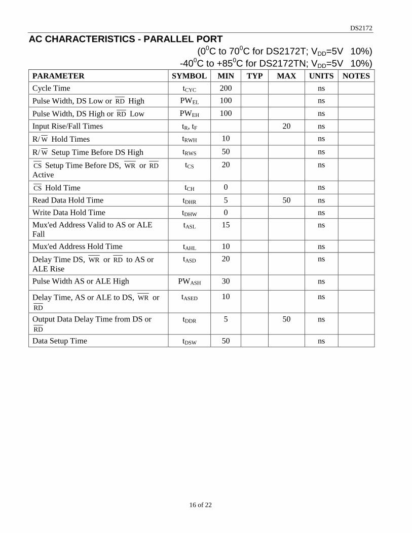
AC CHARACTERISTICS - PARALLEL PORT (00C to 700C for DS2172T; VDD=5V�10%)
-400C to +850C for DS2172TN; VDD=5V�10%)PARAMETER SYMBOL MIN TYP MAX UNITS NOTESCycle Time tCYC 200 nsPulse Width, DS Low or RD High PWEL 100 ns
Pulse Width, DS High or RD Low PWEH 100 nsInput Rise/Fall Times tR, tF 20 nsR/ W Hold Times tRWH 10 ns
R/ W Setup Time Before DS High tRWS 50 ns
CS Setup Time Before DS, WR or RDActive
tCS 20 ns
CS Hold Time tCH 0 nsRead Data Hold Time tDHR 5 50 nsWrite Data Hold Time tDHW 0 nsMux'ed Address Valid to AS or ALEFall
tASL 15 ns
Mux'ed Address Hold Time tAHL 10 nsDelay Time DS, WR or RD to AS orALE Rise
tASD 20 ns
Pulse Width AS or ALE High PWASH 30 ns
Delay Time, AS or ALE to DS, WR orRD
tASED 10 ns
Output Data Delay Time from DS orRD
tDDR 5 50 ns
Data Setup Time tDSW 50 ns

DS2172
17 of 22
INTEL BUS READ AC TIMING (BTS=0) Figure 3
tAHL
tDHRtDDR tASL
tCH
PWEH
PWEL
tASD
tASD
tCYC
PWASH
tASED
tCS
ALE
WR
RD
CS
AD0-AD7

DS2172
18 of 22
INTEL BUS WRITE AC TIMING (BTS=0) Figure 4
tDSWtAHL
tDHW tASL
tCH
PWEH
PWEL
tASD
tASD
tCYC
PWASH
tASED
tCS
ALE
RD
WR
CS
AD0-AD7

DS2172
19 of 22
MOTOROLA BUS AC TIMING (BTS=1) Figure 5
tDHW
tDSW
tAHL
tASL
tCHtAHL
tCS
tASL
tRWS
tDDR tDHR
tRWH
tCYC
PWEHtASED
PWEL
tASD
PWASH
AS
DS
R/W
AD0-AD7(READ)
CS
AD0-AD7(WRITE)

DS2172
20 of 22
AC CHARACTERISTICS - RECEIVE SIDE(00C TO 700C FOR DS2172T; VDD=5V�10%)
-400C to +850C for DS2172TN; VDD=5V�10%)PARAMETER SYMBOL MIN TYP MAX UNITS NOTESRCLK Period tCP 19 nsRCLK Pulse Width tCH
tCL
88
nsns
RDATA Set Up to RCLK Rising tSU1 4 nsRDATA Hold from RCLK Rising tHD1 0 nsRDIS Set Up to RCLK Rising tSU2 4 nsRDIS Hold from RCLK Rising tHD2 0 nsRL and LC Pulse Width tWRL 25 nsRCLK Rise and Fall Times tR, tF 10 ns 1
AC CHARACTERISTICS - TRANSMIT SIDE (00C to 700C for DS2172T; VDD=5V�10%)
-400C to +850C for DS2172TN; VDD=5V�10%)PARAMETER SYMBOL MIN TYP MAX UNITS NOTESTCLK Period tCP 19 nsTCLK Pulse Width tCH
tCL
88
nsns
TDATA Delay from TCLK Rising tDD 9 nsTDIS Set Up to TCLK Rising tSU 4 nsTDIS Hold from TCLK Rising tHD 0 nsTL Pulse Width tWTL 15 nsTL Set Up to TCLK Rising tSTL 4 nsTL Hold Off from TCLK Rising tHTL 0 nsTCLK Rise and Fall Time tR, tF 10 ns 1
NOTE:1. The maximum rise and fall time is either 10 ns or 10% of tCP whichever is less.

DS2172
21 of 22
RECEIVE AC TIMING Figure 6
TRANSMIT AC TIMING Figure 7
NOTE: When TDIS is high about the rising edge of TCLK, TDATA will not be updated and will be held with the previous valve until TDIS is lowabout the rising edge of TCLK.
TRANSMIT AC TIMING FOR THE TL INPUT Figure 8
NOTE: The rising edge of TL causes the internal pattern generation circuitry to be reloaded; the first bit of the new pattern (the shaded one) willappear after two TCLK periods.

DS2172
22 of 22
DS2172 32-PIN TQFP
DIM MIN MAX
A - 1.20
A1 0.05 0.15
A2 0.95 1.05
D 8.80 9.20
D1 7.00 BSC
E 8.80 9.20
E1 7.00 BSC
L 0.45 0.75
e 0.80 BSC
B 0.30 0.45
C 0.09 0.20