black silicon for next-generation infrared · pdf fileblack silicon for next-generation...
TRANSCRIPT
U.S. Army Research, Development and Engineering Command
August 2012
BLACK SILICON FOR NEXT-GENERATION
INFRARED SENSORS
Dr. Jeffrey Warrender
Report Documentation Page Form ApprovedOMB No. 0704-0188
Public reporting burden for the collection of information is estimated to average 1 hour per response, including the time for reviewing instructions, searching existing data sources, gathering andmaintaining the data needed, and completing and reviewing the collection of information. Send comments regarding this burden estimate or any other aspect of this collection of information,including suggestions for reducing this burden, to Washington Headquarters Services, Directorate for Information Operations and Reports, 1215 Jefferson Davis Highway, Suite 1204, ArlingtonVA 22202-4302. Respondents should be aware that notwithstanding any other provision of law, no person shall be subject to a penalty for failing to comply with a collection of information if itdoes not display a currently valid OMB control number.
1. REPORT DATE AUG 2012 2. REPORT TYPE
3. DATES COVERED 00-00-2012 to 00-00-2012
4. TITLE AND SUBTITLE Black Silicon for Next-Generation Infrared Sensors
5a. CONTRACT NUMBER
5b. GRANT NUMBER
5c. PROGRAM ELEMENT NUMBER
6. AUTHOR(S) 5d. PROJECT NUMBER
5e. TASK NUMBER
5f. WORK UNIT NUMBER
7. PERFORMING ORGANIZATION NAME(S) AND ADDRESS(ES) U.S. Army Research, Development and Engineering Command,Picatinny Arsenal,NJ,07806-5000
8. PERFORMING ORGANIZATIONREPORT NUMBER
9. SPONSORING/MONITORING AGENCY NAME(S) AND ADDRESS(ES) 10. SPONSOR/MONITOR’S ACRONYM(S)
11. SPONSOR/MONITOR’S REPORT NUMBER(S)
12. DISTRIBUTION/AVAILABILITY STATEMENT Approved for public release; distribution unlimited
13. SUPPLEMENTARY NOTES Presented at the 2nd Multifunctional Materials for Defense Workshop in conjunction with the 2012 AnnualGrantees’/Contractors’ Meeting for AFOSR Program on Mechanics of Multifunctional Materials &Microsystems Held 30 July - 3 August 2012 in Arlington, VA. Sponsored by AFRL, AFOSR, ARO, NRL,ONR, and ARL.
14. ABSTRACT
15. SUBJECT TERMS
16. SECURITY CLASSIFICATION OF: 17. LIMITATION OF ABSTRACT Same as
Report (SAR)
18. NUMBEROF PAGES
34
19a. NAME OFRESPONSIBLE PERSON
a. REPORT unclassified
b. ABSTRACT unclassified
c. THIS PAGE unclassified
Standard Form 298 (Rev. 8-98) Prescribed by ANSI Std Z39-18
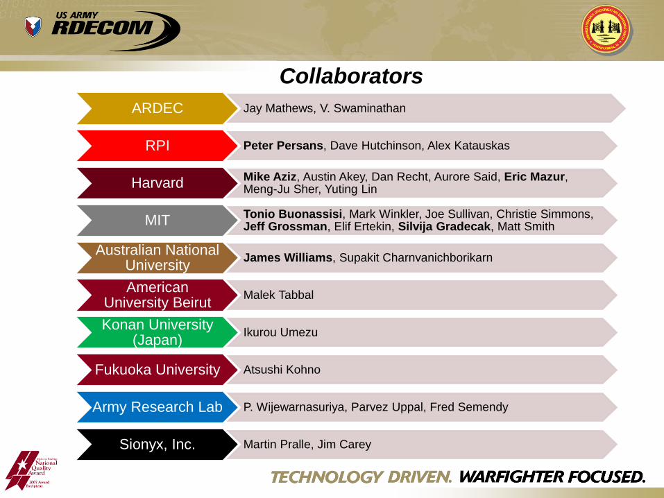
Collaborators
ARDEC Jay Mathews, V. Swaminathan
RPI Peter Persans, Dave Hutchinson, Alex Katauskas
Harvard Mike Aziz, Austin Akey, Dan Recht, Aurore Said, Eric Mazur, Meng-Ju Sher, Yuting Lin
MIT Tonio Buonassisi, Mark Winkler, Joe Sullivan, Christie Simmons, Jeff Grossman, Elif Ertekin, Silvija Gradecak, Matt Smith
Australian National University
James Williams, Supakit Charnvanichborikarn
American University Beirut
Malek Tabbal
Konan University (Japan)
Ikurou Umezu
Fukuoka University Atsushi Kohno
Army Research Lab P. Wijewarnasuriya, Parvez Uppal, Fred Semendy
Sionyx, Inc. Martin Pralle, Jim Carey
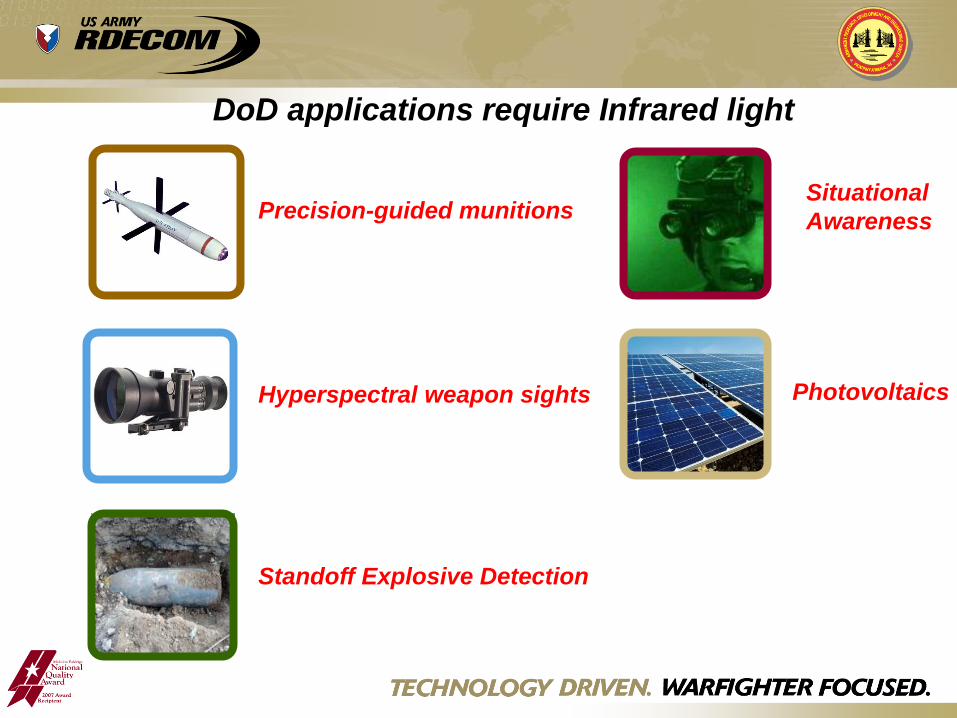
Situational
Awareness
Hyperspectral weapon sights
Precision-guided munitions
Standoff Explosive Detection
Photovoltaics
DoD applications require Infrared light
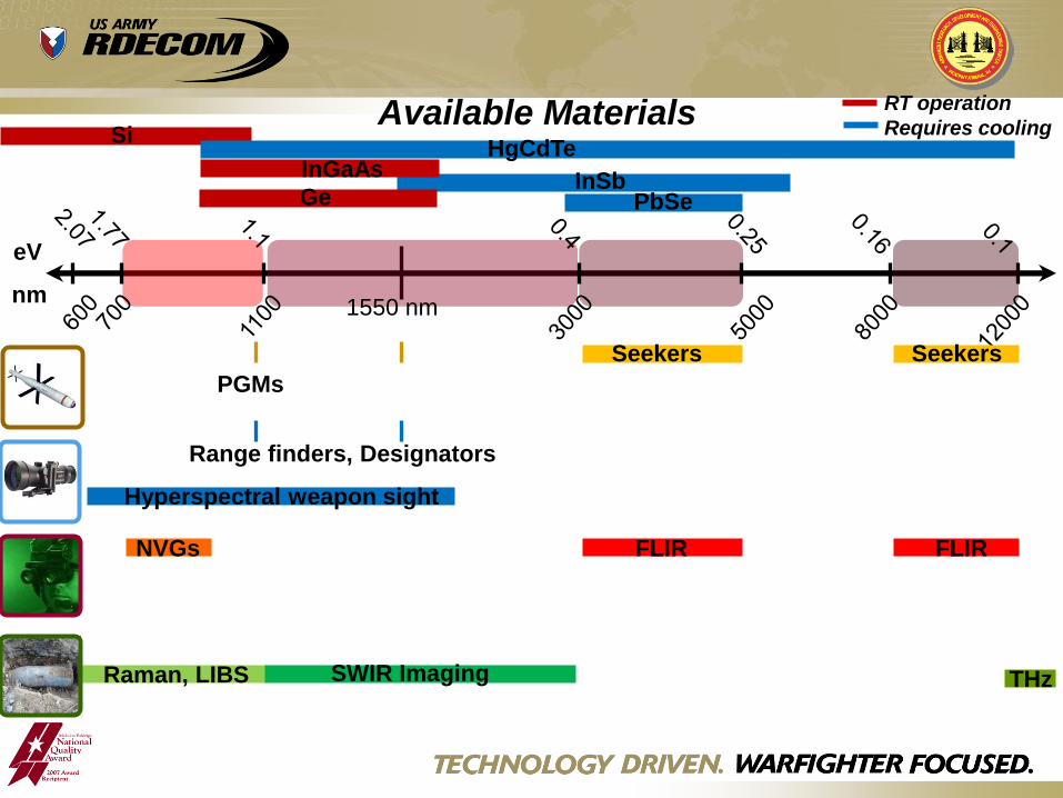
Raman, LIBS SWIR Imaging
NVGs FLIR FLIR
THz
PGMs
eV
nm
Seekers Seekers
Range finders, Designators
Hyperspectral weapon sight
Si
InSb InGaAs
PbSe
HgCdTe
Ge
RT operation
Requires cooling Available Materials
1550 nm

Silicon-based IR optoelectronics
Silicon is…
Ubiquitous
Inexpensive
Well-characterized
Easy to integrate with readout circuitry
Non-absorbing for wavelengths > 1100 nm
+
-
Can we dope Si to see IR response?
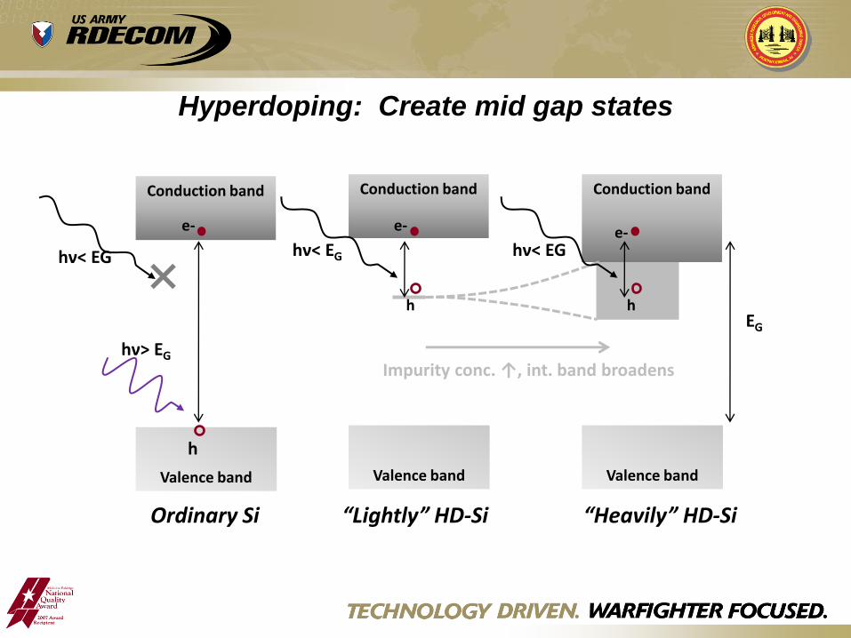
Valence band
Conduction band
318
hν> EG
EG
hν< EG
e-
h
Valence band
Conduction band
e-
h
hν< EG
Valence band
Conduction band
hν< EG
Ordinary Si “Lightly” HD-Si “Heavily” HD-Si
Impurity conc. ↑, int. band broadens
e-
h
Hyperdoping: Create mid gap states
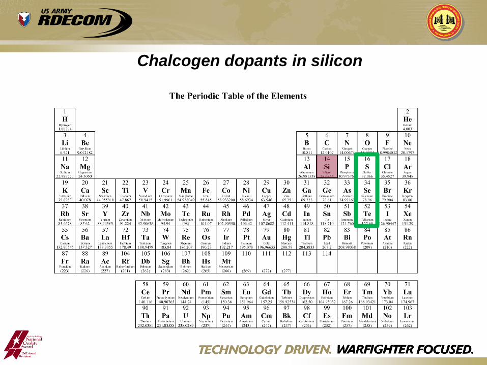
Chalcogen dopants in silicon
The Periodic Table of the Elements
I 2 B He
"'".'"" .._,hn• ) / 1!)':')4 4J•:l)
3 4 5 6 " R <) 10 ' l.i 1\e n c :\1 0 F Ne
l ,oh"n ~nl lotn ......... n rto" v ... .,.... ' "'h"' ~)""'"' ' "" i: .'>-11 '/.!11.!1 :>2 J(!.~l t 11-'o " ' H.{ooj ((' II,'NMil:~z :;~;. p•,)7
I I 12 I '' ·' 14 15 H• 17 I X
Na Mg AI Si p s Cl Ar ... ..... .... ':f"'"" ....... ,.,., '··:·:~ .. ""''t'lro)'• : ....... <1•0) •"'• ( '(;>•
12.'Jb'>:'":l l<IJtJ.s-J 2C..<;~ J JJ8 j t\:1737 J::Jt(o:i :t~A~l:' J.'J!."''~
I 'J 20 21 ,, <• 2:~ 24 25 2() 27 2X 29 3(1 31 32 :;,, 34 35 3(•
K Ca Sc T i v Cr .\·In Fe Co l\i C 11 Zn Ga Gc As Sc Br Kr (,, ... ,,, v.· .. ,,." '''"'"" v. '~""" • ltr.~""'' ..... ,.?_ ... ·~ .... .._ • . t .. ! t)i<(~ ·;.u <-•""'' '""''""""' ............ .::,, ... .,,.
"··~ " "'' :.'>'1" " .!').1:~>113 4!l/J:'!' 4-I.')JS!.'!tl ~:'.~!>? S.I!.'J4 1~ ~ J.')<JQJ ~-1.'/Jl!(Jol') 55.~! J~.·;:>JZ!IO !~.(1'):04 (o),S¥.o ()5 • .!') {o')::-2:l ; ;u :J N.'ll l 7~.'J6 i').'Xl~ ,i)~l)
·~ .~ I 3R :19 40 4 1 42 41 44 45 46 47 4~ 41) 50 51 52 53 54
Rb Sr y Zr Nb Mo Tc Ru Rh Pd Ag Cd Tn Sn Sb Te 1 Xe ll<olo~"·" Su.~""'' ~IM"tl y,_,, .. ,., .............
''"'"~""' ..... .,~ . " YoiJ>w.,., n ll ,ol o•o ,.,~ . .-.. ~, "- t :M .. , , ''''"'' ... ·' •'" •J ·~ ·" .... '"""'"" x .... ...
~ . .v..;~ 117.1!:; .ilL'J!l~!iS '}1.?24 'J! .'JI:Mt!. ')$.'.14 ( ')II \ 101 .tJ: 1(12.~'[•.$$0 h•f>A:i: W:' . .i(.._~ 11!.411 1 14.111~ l!K:U! !2 1.7(1(: :::6.'}1);44~ nu~·
55 56 57 !2 7J 74 i S "76 77 'JK 79 K(l ~ I 82 ~· ,> R5 R6 Cs Ra T.a H f Ta \\' Re Os Tr 1'1 Au Hg Tl Pb Ri Po At Rn r.-:., .. n:o~ .. ,, .............. ''"''I''" r,,,.,..,,.. T'h'>J$11> • k "eool ot> n .,... ,,., loll .... ,\.,;,,, ( h iJ . ....,,.,,. .,..1'1 ..... 1...-ol "'"'"''' ">'""'" J.W ~OO) II""'
U.!.90!iU n•-'2' n .j(.'J+)jS r:'~.:w l!ii).Y.I:''i !l~:!. :N l lv.o.::.:J:' (";11/2:! 1 ~:!.2 !. :' l'i$.0:'~ IW1.~z65!l :i:OIJ.$;> :::o..t:!.!!J.) ::07.2 ZC« .\Mt•:!:i .!t!9 !!I OJ f:!Z:!•
87 ~8 ~9 104 105 106 107 10~ 109 llO Ill 112 113 114 F'r Ra i\ C Rf' Db Sg llh Hs IVIt
r ... ,._ .. ., tt..J,.,. ..... , ....... lla.-h.::ru-J,. •. :-.;, .. ,, Sulu:ti"• 3:cinono ~:. ..... ~>~.; .. .,.;.,. i1:!Ji o:::.H::• ( 2:!7:. ~(•I I ;:U~o.:) {!6Ji (~ (':= :· !Zi.l$ 1 (:! ti(l) ;1(l;l) m::> .:.:~·:·
58 59 60 61 62 63 64 65 66 67 68 69 70 7 1 Ce T•r Nd Pm Srn F.u Gel T b Dy Ho F.r Tm Yb Lu ......... h ·->•:<bni•n. l4c>-t-ni ,.., t>.or.c .. ~U.. :t ... ., ..... £ .......... O.Jol,;,,., ;....;;...,. :>....---..... l-l;looion, Z:l:i .o• : tu!un • .. , •• otw .. t .,. .• tr.l
1-KU J() 1-kl.')t:l:"{o:i 14U4 IH$ 1 l.'CI.:lll l ! l :)M UJ.25 J jb.'J?5:f~ 1(:2.! 0 I M.:•:Jt•~1 1(0:'. :::6 l(IK,'JHl l J]J!:Jof l :'of.$67
90 91 92 9'' • J 94 95 96 97 98 99 100 101 102 103 Th Pa u :Xp Pu Am Cm Bk Cf Es Fm Md No Lr
Th:nom l'n·:o.o.•ioiun u ......... s'""'"""' r: . ~., ..... ,\~~~~~;,. ~~~ l!ul<:loon \:Ojc:,,., ,., e;. ...... -. .,.. l'.::n iu n r.::.nJ:I. .. ,.r. Ni:..t;.,, l·;;~';"' :B:!.fO:!X! ::::!J .t\3}~:-1 :!:.>~(!::.li'J IH71 l:! .:l:h ., , ,·; ,,;·, 1:!511 C5:! 'o !:i: ~ ~· (15~> !! !''il l
TECHNOWGY DRIVEN. WARRGHTER FOCUSED.
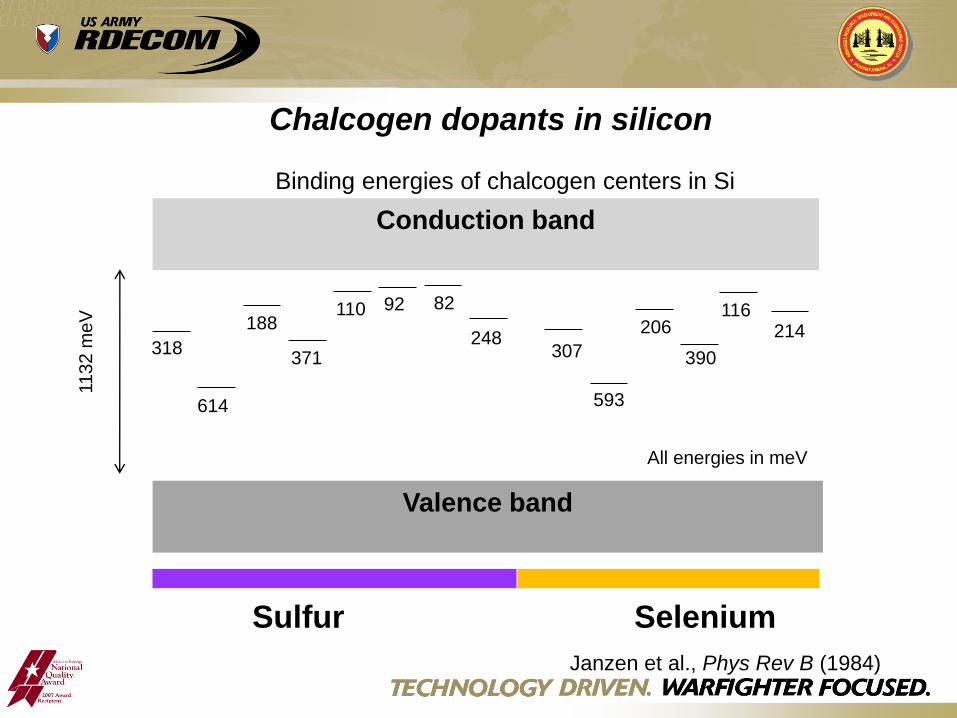
Valence band
Conduction band
Sulfur Selenium
318
614
110 188
371
92 82
248 307
593
206
390
214
116
All energies in meV
Janzen et al., Phys Rev B (1984)
Chalcogen dopants in silicon
11
32
me
V
Binding energies of chalcogen centers in Si
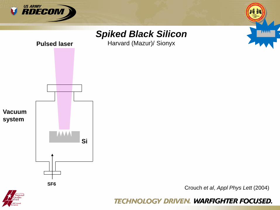
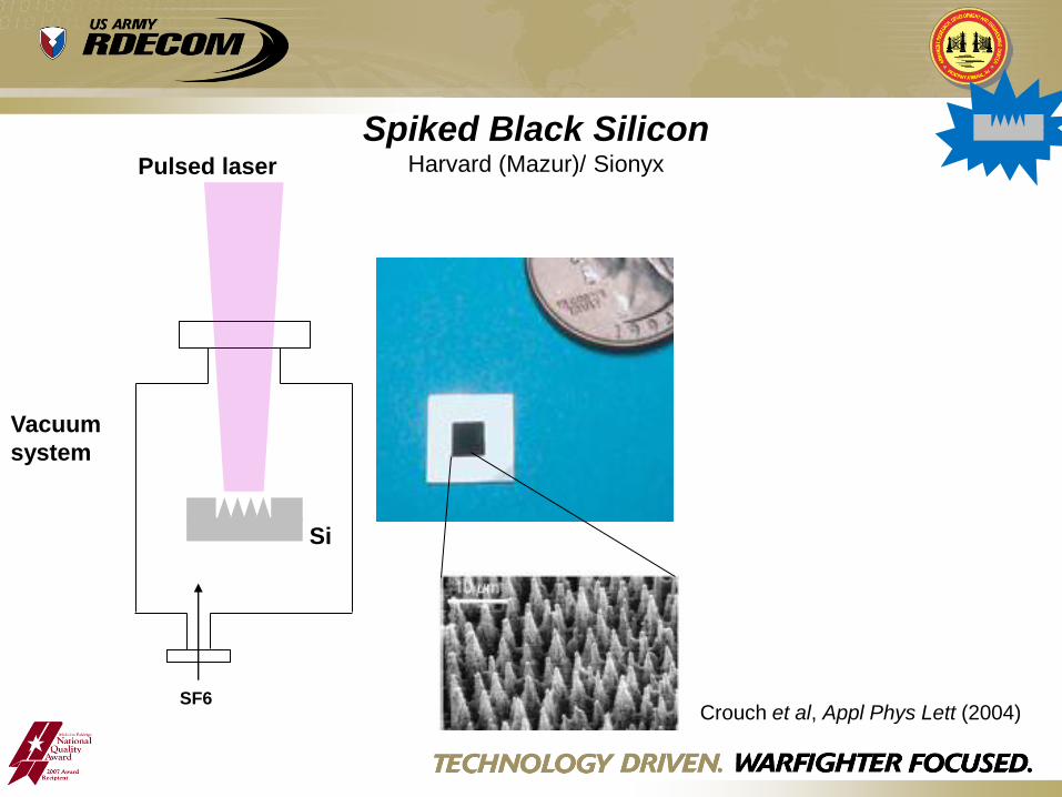
Spiked Black Silicon Harvard (Mazur)/ Sionyx
SF6
Si
Pulsed laser
Vacuum
system
Crouch et al, Appl Phys Lett (2004)
Spiked Black Silicon Harvard (Mazur)/ Sionyx
SF6
Si
Pulsed laser
Vacuum
system
Crouch et al, Appl Phys Lett (2004)
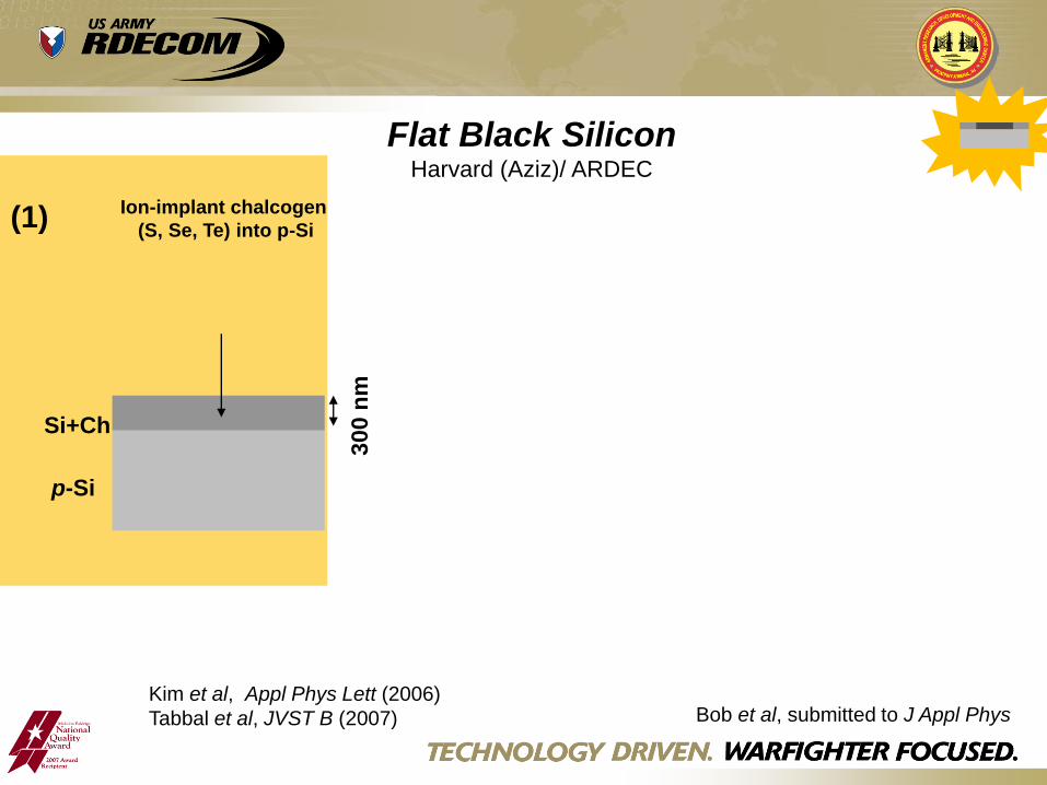
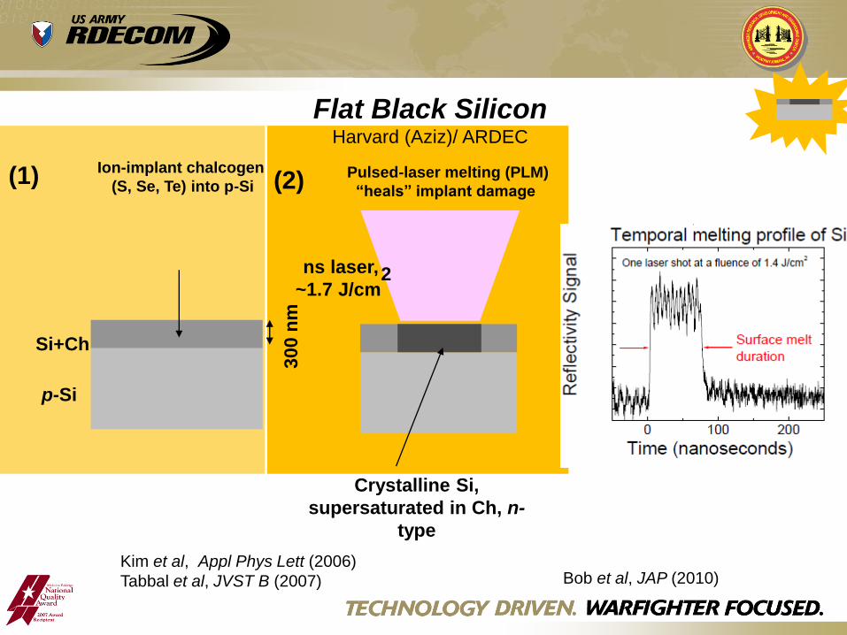
p-Si
Si+Ch
300 n
m
Ion-implant chalcogen
(S, Se, Te) into p-Si (1)
Bob et al, submitted to J Appl Phys Kim et al, Appl Phys Lett (2006)
Tabbal et al, JVST B (2007)
Flat Black Silicon Harvard (Aziz)/ ARDEC
p-Si
Si+Ch
300 n
m
Ion-implant chalcogen
(S, Se, Te) into p-Si (1) Pulsed-laser melting (PLM)
“heals” implant damage
Crystalline Si,
supersaturated in Ch, n-
type
ns laser,
~1.7 J/cm2
(2)
Bob et al, JAP (2010) Kim et al, Appl Phys Lett (2006)
Tabbal et al, JVST B (2007)
Flat Black Silicon Harvard (Aziz)/ ARDEC
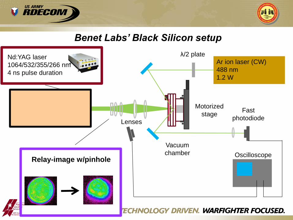
Ar ion laser (CW)
488 nm
1.2 W
Relay-image w/pinhole
Lenses
Vacuum
chamber
Motorized
stage
λ/2 plate
Fast
photodiode
Oscilloscope
Nd:YAG laser
1064/532/355/266 nm
4 ns pulse duration
Benet Labs’ Black Silicon setup

Structure Optoelectronic
Properties
Absorption
Electronic
properties
Device
Properties
6.1 6.2
Characterization Logical Flow
• Dopant profile
• Surface roughness
• Crystallinity
• Local dopant
environment
• Absorption vs.
wavelength
• Depth profile
• Modeling
• Carrier sign,
concentration,
mobility, lifetime
• Hall effect
• Photoconductivity
• Spectral responsivity
• Quantum Efficiency
• IV curves
• Gain
• Detectivity
• Noise Equivalent
Power
• Dark current
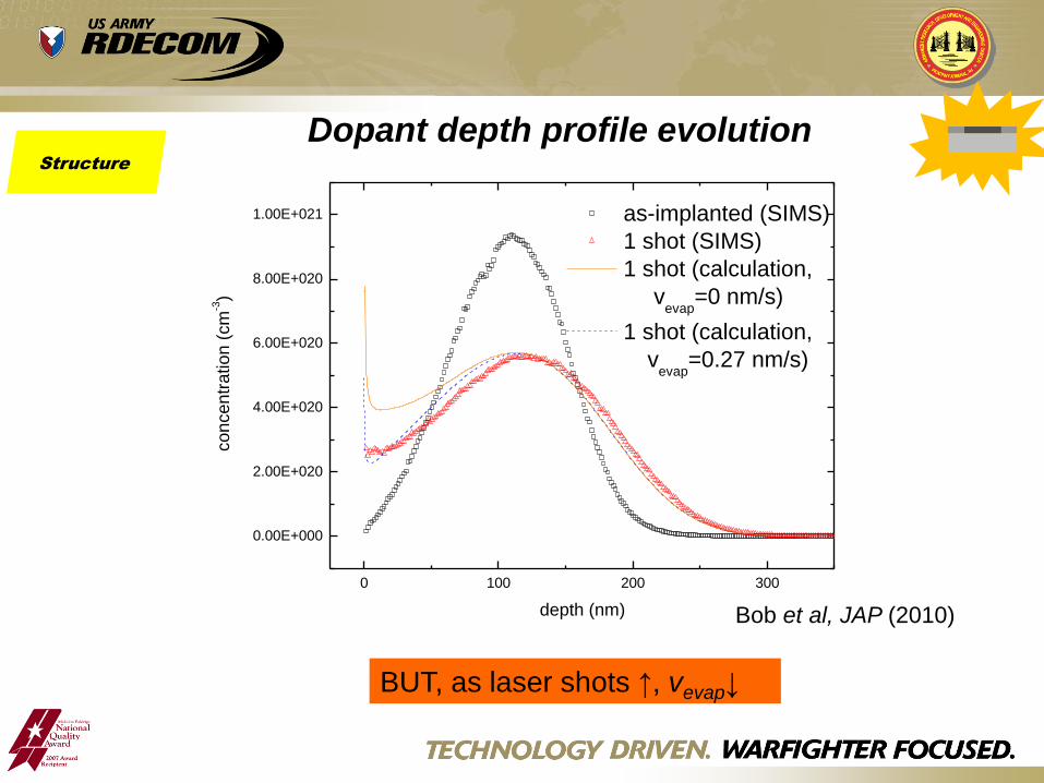
0 100 200 300
0.00E+000
2.00E+020
4.00E+020
6.00E+020
8.00E+020
1.00E+021
con
cen
tra
tio
n (
cm
-3)
depth (nm)
as-implanted (SIMS)
1 shot (SIMS)
1 shot (calculation,
vevap
=0 nm/s)
1 shot (calculation,
vevap
=0.27 nm/s)
Bob et al, JAP (2010)
BUT, as laser shots ↑, vevap↓
Structure
Dopant depth profile evolution
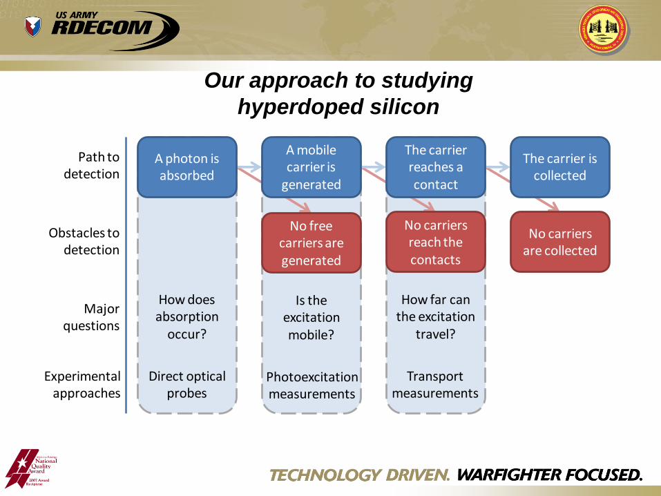
Major questions
How does absorption
occur?
Is the excitationmobile?
How far can the excitation
travel?
Experimentalapproaches
Direct optical probes
Transport measurements
No free carriers are generated
No carriers reach the contacts
No carriers are collected
Obstacles to detection
A photon is absorbed
A mobile carrier is
generated
The carrier reaches a contact
The carrier is collected
Path to detection
Photoexcitationmeasurements
Our approach to studying
hyperdoped silicon

Absorption
Absorption
Winkler, Ph.D. thesis, Harvard (2010)
U US ARIIIIY ft~ ·v IIDEC~
photon energy (eV)
1 25 3 2 1 0.5 . .---r-r-----.---------~~----
Q)
g 1.00 ro -e-@ 0.75 .0 ro
"@ N 0.50 ro E ~
0 0.25 c
A = (1 - R - T) I (1 - R)
fs-laser doping , ,
lon implant+PLM doping
,..,1020 em""' chalcogens
silicon w fer
S.Si
S:Si
o ~------~~------~--_.~--~
0 1 2 wavelength (J.Im)
3
TECHNOWGY DRIVEN. WARRGHTER FOCUSED.
800 1000 1200 14000.01
0.1
1
10
100
1000 Si diode
Si:S, 12V, no anneal
wavelength (nm)
Re
spo
nsiv
ity (
A/W
)
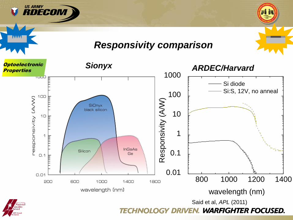
Sionyx ARDEC/Harvard
Responsivity comparison
Optoelectronic
Properties
Said et al, APL (2011)
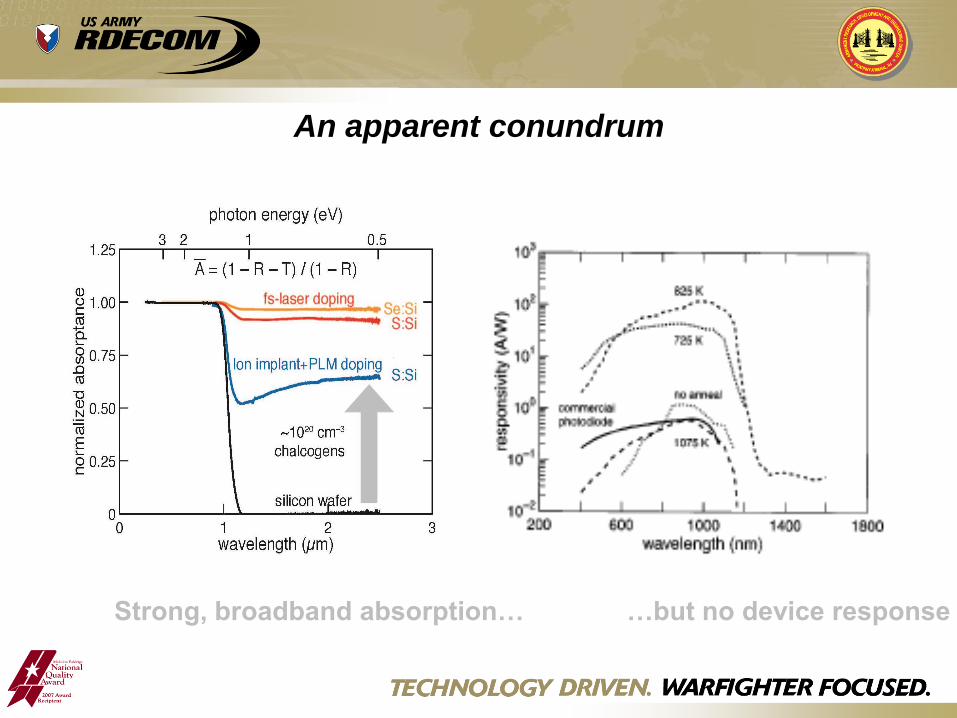
Strong, broadband absorption… …but no device response
An apparent conundrum
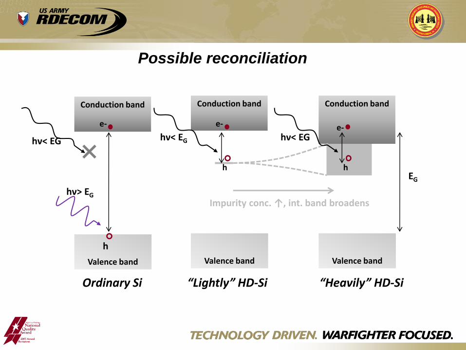
Valence band
Conduction band
318
hν> EG
EG
hν< EG
e-
h
Valence band
Conduction band
e-
h
hν< EG
Valence band
Conduction band
hν< EG
Ordinary Si “Lightly” HD-Si “Heavily” HD-Si
Impurity conc. ↑, int. band broadens
e-
h
Possible reconciliation
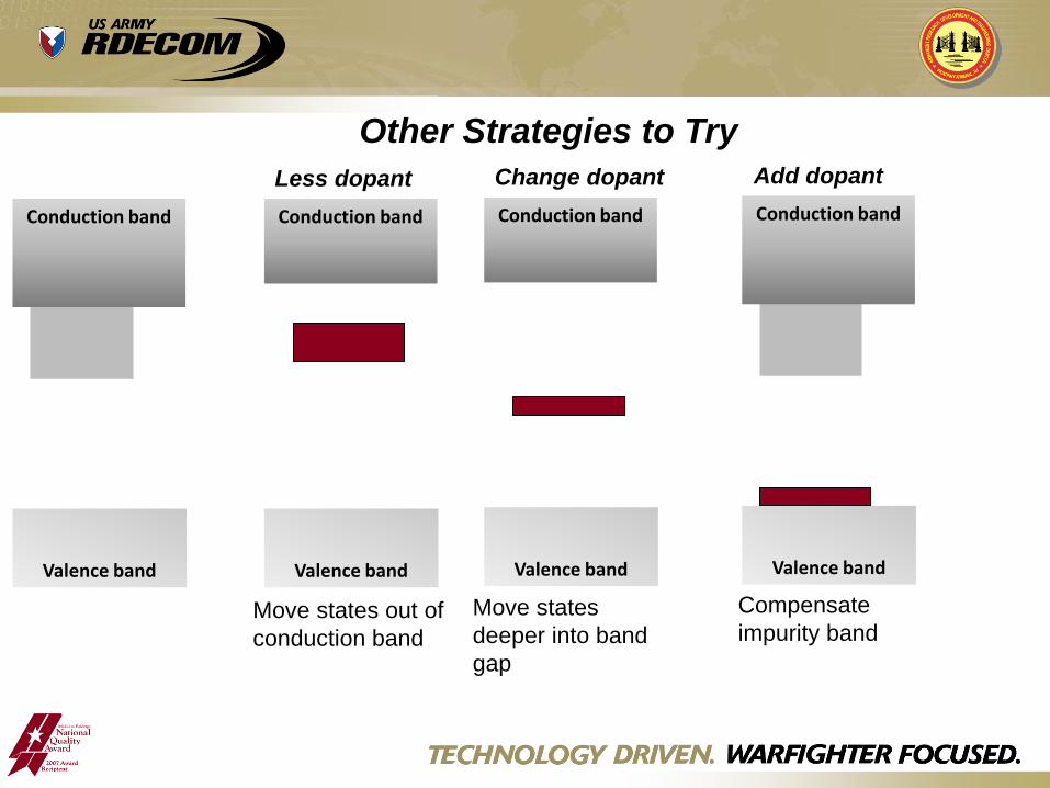
Other Strategies to Try
Valence band
Conduction band
Valence band
Conduction band
Less dopant
Valence band
Conduction band
Change dopant
Move states out of
conduction band
Move states
deeper into band
gap
Valence band
Conduction band
Add dopant
Compensate
impurity band

Stakeholders Research Groups
The Larger Black Silicon Universe
ARDEC-Benet
Warrender
RPI
Persans
Harvard
Aziz
MIT
Buonassisi
Harvard
Mazur
MIT
Gradecak
MIT
Grossman
Illinois
Ertekin
Extended IR response,
optoelectronic
charazterization
Characterization of fs-
structured Black Silicon
First principles modeling
Sionyx
Pralle, Carey Commercialization
CERDEC-
NVESD
USMC
ONR
White Sands
Missile Range
ARDEC
System
X
X X
X X
X
X X
Digital
Nightvision
CLRF
DETECT,
CLRF
Airborne
Laser
Precision-
guided
23 ¼ Moon, March 30, 2012, 8:40PM
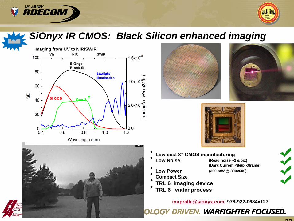
• Low cost 8” CMOS manufacturing • Low Noise (Read noise ~2 e/pix)
(Dark Current <8e/pix/frame) • Low Power (300 mW @ 800x600)
• Compact Size • TRL 6 imaging device • TRL 6 wafer process
[email protected], 978-922-0684x127
Imaging from UV to NIR/SWIR
SiOnyx
Black Si
Si CCD Gen 3 I2
Starlight
illumination
Vis NIR SWIR
SiOnyx IR CMOS: Black Silicon enhanced imaging
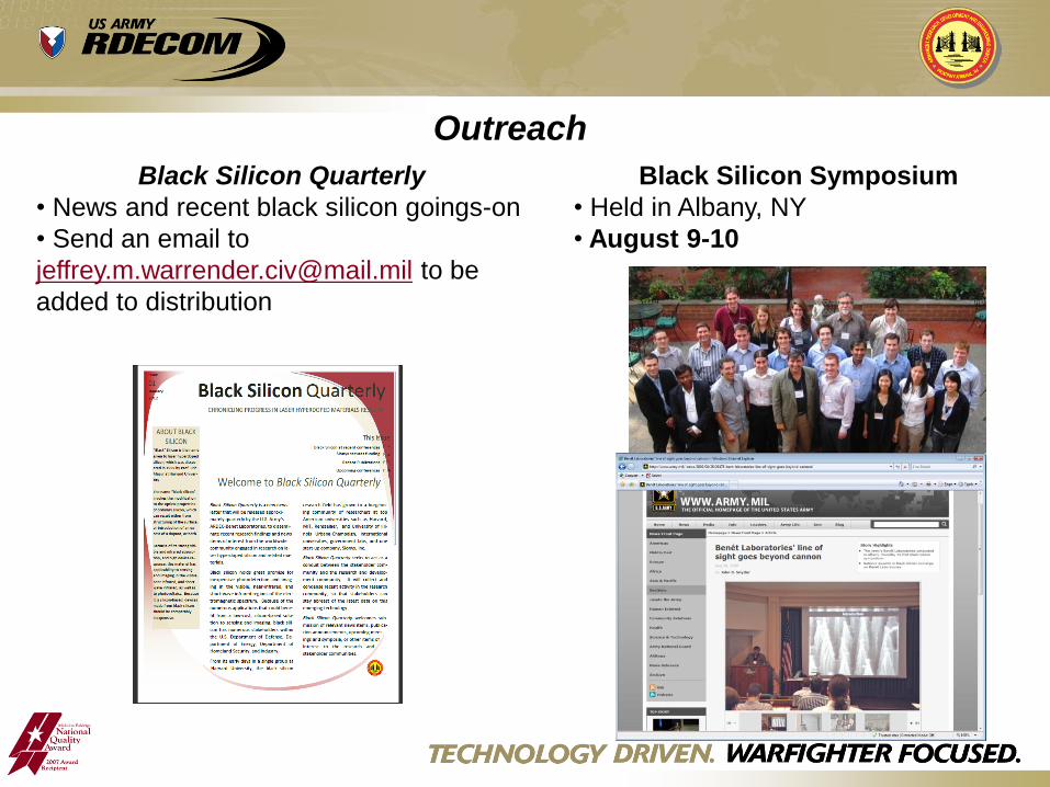
Black Silicon Symposium
• Held in Albany, NY
• August 9-10
Outreach
Black Silicon Quarterly
• News and recent black silicon goings-on
• Send an email to
[email protected] to be
added to distribution
Summary and Outlook
• Laser hyperdoped “black” silicon can be made by two different
approaches
• Similar properties
• “Flat” black silicon easier to study
• Strong sub band gap absorption
• High EQE out to 1200 nm
• ARDEC seeks to extend strong device response to 1700 nm
• Fundamental and practical questions abound

BACKUP SLIDES
Research interests at Benet
Extending black silicon’s IR response
Characterizing the properties of ns-spiked black Si
Exploring broader slice of parameter space
Non-chalcogen dopants, thick layers, 5 ns pulses, non-
UV wavelengths
Increasing process cleanliness
Black Si photovoltaics
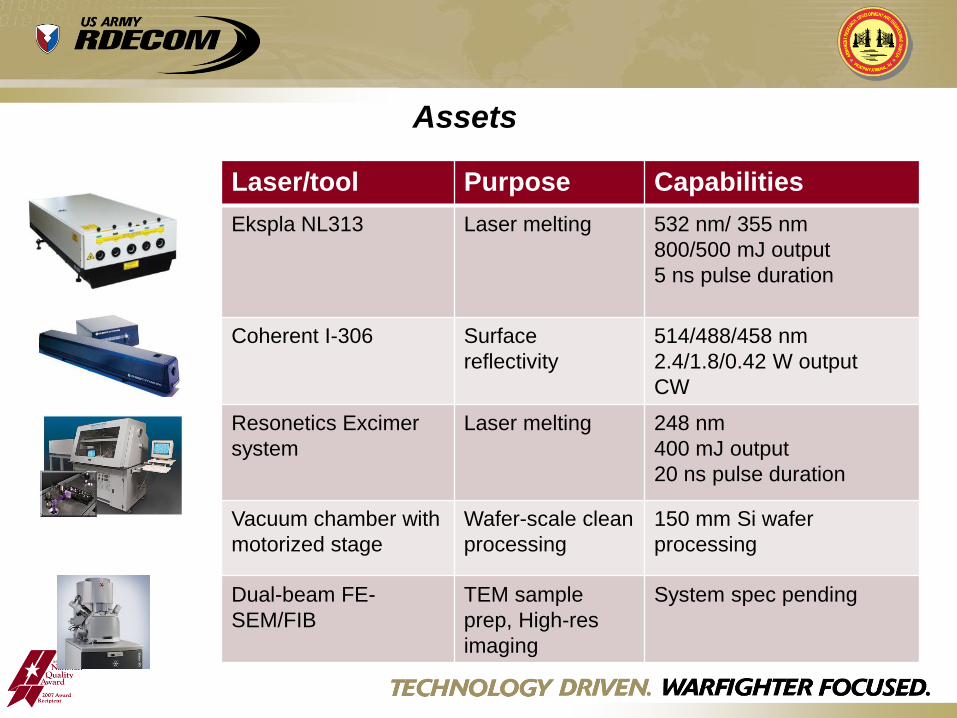
Laser/tool Purpose Capabilities
Ekspla NL313 Laser melting 532 nm/ 355 nm
800/500 mJ output
5 ns pulse duration
Coherent I-306 Surface
reflectivity
514/488/458 nm
2.4/1.8/0.42 W output
CW
Resonetics Excimer
system
Laser melting 248 nm
400 mJ output
20 ns pulse duration
Vacuum chamber with
motorized stage
Wafer-scale clean
processing
150 mm Si wafer
processing
Dual-beam FE-
SEM/FIB
TEM sample
prep, High-res
imaging
System spec pending
Assets

Gain is spatially inhomogeneous Optoelectronic
Properties
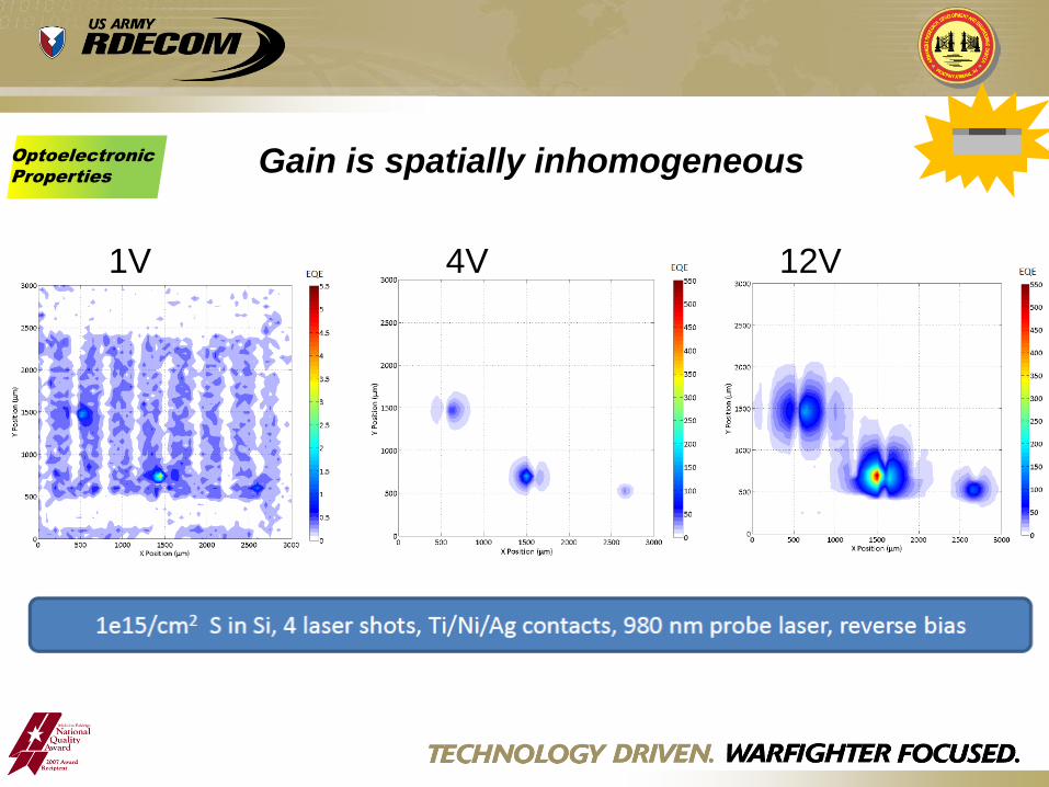
Gain is spatially inhomogeneous
1V 4V 12V
Optoelectronic
Properties
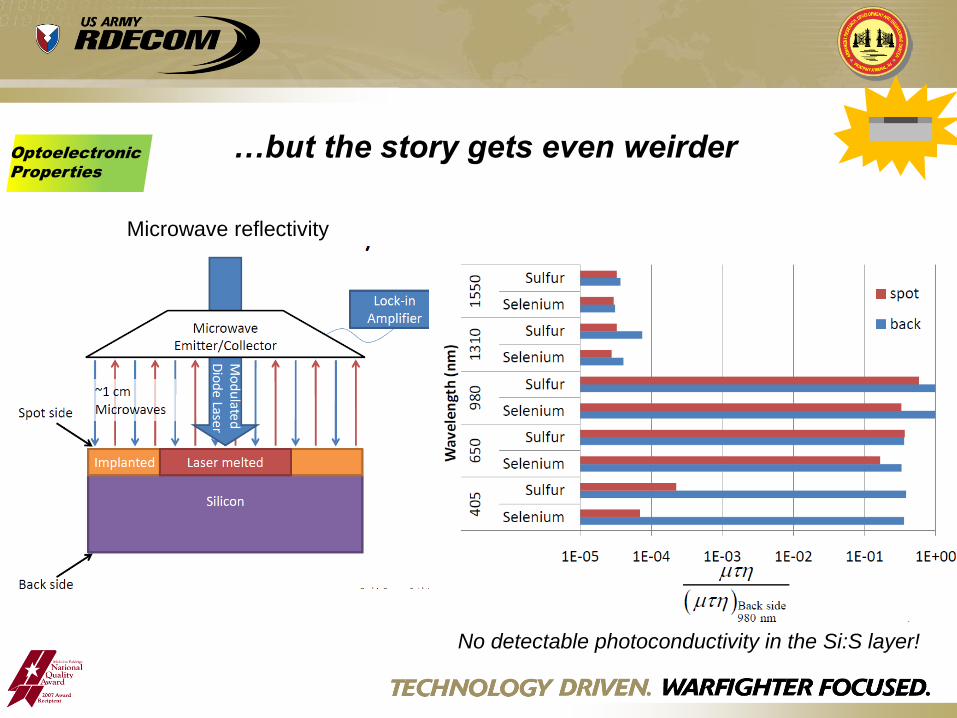
…but the story gets even weirder Optoelectronic
Properties
Microwave reflectivity
No detectable photoconductivity in the Si:S layer!
V
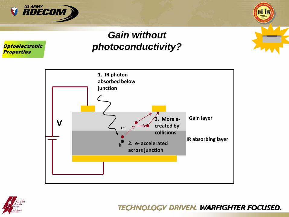
1. IR photon absorbed below junction
2. e- accelerated across junction
e-
h
Gain layer
IR absorbing layer
3. More e- created by collisions
Gain without
photoconductivity? Optoelectronic
Properties
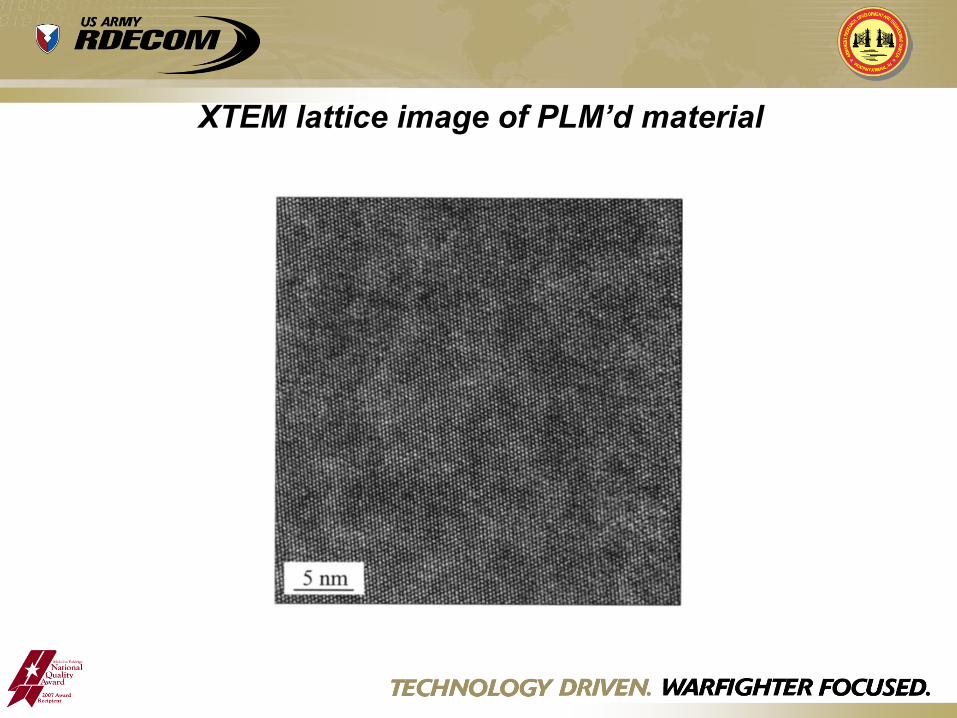
XTEM lattice image of PLM’d material
U US ARIIIIY ft~ ·v IIDEC~
TECHNOWGY DRIVEN. WARRGHTER FOCUSED.

U US ARIIIIY ft~ ·v IIDEC~
Data were converted to signal per (pump photons per second)
photoinduced , microwave
reflectivity
pump energy per photon
Pump power 1-Reflectance
--Signal/ {pump
photons per second)
CD.a Cept1n Ceprg ( Cepo )x(photons! ~ec ) x ('I) ----- - = · = Ceprl] photo._n_s_/ s_ec __ P_h-...otons~~/~s=ec~~p:h~o:to:n:s~/ s:e:c ___ ~p:h~ot:o~n:s /~s:e~c -~~2~-=
Constant dependent on apparatus not sample or pump
Taking t he rat io of two measurements removes t he influe nce of the expe rimental apparatus (C cancels out)
TECHNOWGY DRIVEN. WARRGHTER FOCUSED.