bluenrg-1, 2 dev kits user manual - home - …content/translations/en.dm00298232.pdfbluenrg-1, 2 dev...
TRANSCRIPT
IntroductionThe BlueNRG-1, BlueNRG-2 devices are low power Bluetooth® smart system on chip, compliant with the Bluetooth®
specification and supporting master, slave and simultaneous master-and-slave roles. Further, BlueNRG-2 supports theBluetooth Low Energy data length extension feature.
The following BlueNRG-1, BlueNRG-2 kits are available:1. BlueNRG-1 development platforms (order code: STEVAL-IDB007V1, STEVAL-IDB007V2)2. BlueNRG-2 development platforms (order code: STEVAL-IDB008V1, STEVAL-IDB008V2)
The STEVAL-IDB007Vx, STEVAL-IDB008Vx also provide a set of hardware resources for a wide range of application scenarios:sensor data (accelerometer, pressure and temperature sensor), remote control (buttons and LEDs) and debug messagemanagement through USB virtual COM. Three power options are available (USB only, battery only and external power supplyplus USB) for high application development and testing flexibility.
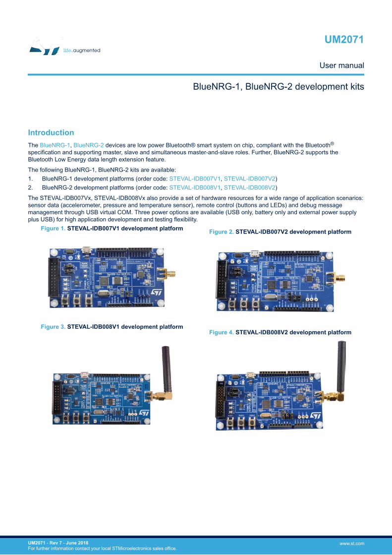
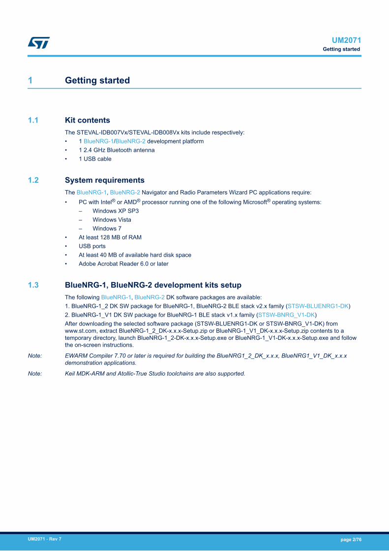
Figure 1. STEVAL-IDB007V1 development platform Figure 2. STEVAL-IDB007V2 development platform
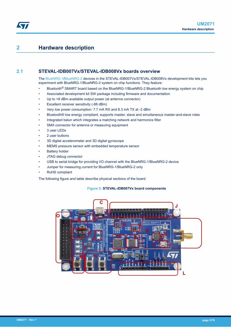
Figure 3. STEVAL-IDB008V1 development platformFigure 4. STEVAL-IDB008V2 development platform
BlueNRG-1, BlueNRG-2 development kits
UM2071
User manual
UM2071 - Rev 7 - June 2018For further information contact your local STMicroelectronics sales office.
www.st.com
1 Getting started
1.1 Kit contentsThe STEVAL-IDB007Vx/STEVAL-IDB008Vx kits include respectively:• 1 BlueNRG-1/BlueNRG-2 development platform• 1 2.4 GHz Bluetooth antenna• 1 USB cable
1.2 System requirementsThe BlueNRG-1, BlueNRG-2 Navigator and Radio Parameters Wizard PC applications require:• PC with Intel® or AMD® processor running one of the following Microsoft® operating systems:
– Windows XP SP3– Windows Vista– Windows 7
• At least 128 MB of RAM• USB ports• At least 40 MB of available hard disk space• Adobe Acrobat Reader 6.0 or later
1.3 BlueNRG-1, BlueNRG-2 development kits setupThe following BlueNRG-1, BlueNRG-2 DK software packages are available:1. BlueNRG-1_2 DK SW package for BlueNRG-1, BlueNRG-2 BLE stack v2.x family (STSW-BLUENRG1-DK)2. BlueNRG-1_V1 DK SW package for BlueNRG-1 BLE stack v1.x family (STSW-BNRG_V1-DK)After downloading the selected software package (STSW-BLUENRG1-DK or STSW-BNRG_V1-DK) fromwww.st.com, extract BlueNRG-1_2_DK-x.x.x-Setup.zip or BlueNRG-1_V1_DK-x.x.x-Setup.zip contents to atemporary directory, launch BlueNRG-1_2-DK-x.x.x-Setup.exe or BlueNRG-1_V1-DK-x.x.x-Setup.exe and followthe on-screen instructions.
Note: EWARM Compiler 7.70 or later is required for building the BlueNRG1_2_DK_x.x.x, BlueNRG1_V1_DK_x.x.xdemonstration applications.
Note: Keil MDK-ARM and Atollic-True Studio toolchains are also supported.
UM2071Getting started
UM2071 - Rev 7 page 2/76
2 Hardware description
2.1 STEVAL-IDB007Vx/STEVAL-IDB008Vx boards overviewThe BlueNRG-1/BlueNRG-2 devices in the STEVAL-IDB007Vx/STEVAL-IDB008Vx development kits lets youexperiment with BlueNRG-1/BlueNRG-2 system on chip functions. They feature:• Bluetooth® SMART board based on the BlueNRG-1/BlueNRG-2 Bluetooth low energy system on chip• Associated development kit SW package including firmware and documentation• Up to +8 dBm available output power (at antenna connector)• Excellent receiver sensitivity (-88 dBm)• Very low power consumption: 7.7 mA RX and 8.3 mA TX at -2 dBm• Bluetooth® low energy compliant, supports master, slave and simultaneous master-and-slave roles• Integrated balun which integrates a matching network and harmonics filter• SMA connector for antenna or measuring equipment• 3 user LEDs• 2 user buttons• 3D digital accelerometer and 3D digital gyroscope• MEMS pressure sensor with embedded temperature sensor• Battery holder• JTAG debug connector• USB to serial bridge for providing I/O channel with the BlueNRG-1/BlueNRG-2 device• Jumper for measuring current for BlueNRG-1/BlueNRG-2 only• RoHS compliant
The following figure and table describe physical sections of the board.
Figure 5. STEVAL-IDB007Vx board components
UM2071Hardware description
UM2071 - Rev 7 page 3/76
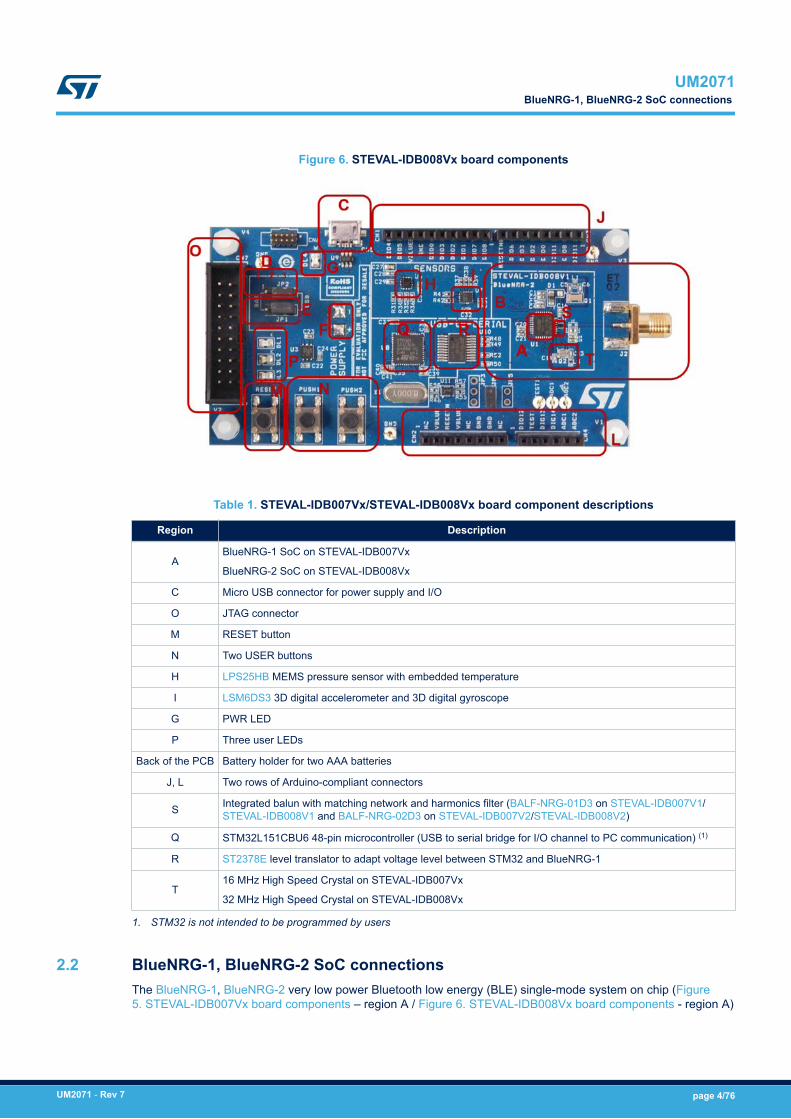
Figure 6. STEVAL-IDB008Vx board components
Table 1. STEVAL-IDB007Vx/STEVAL-IDB008Vx board component descriptions
Region Description
ABlueNRG-1 SoC on STEVAL-IDB007Vx
BlueNRG-2 SoC on STEVAL-IDB008Vx
C Micro USB connector for power supply and I/O
O JTAG connector
M RESET button
N Two USER buttons
H LPS25HB MEMS pressure sensor with embedded temperature
I LSM6DS3 3D digital accelerometer and 3D digital gyroscope
G PWR LED
P Three user LEDs
Back of the PCB Battery holder for two AAA batteries
J, L Two rows of Arduino-compliant connectors
S Integrated balun with matching network and harmonics filter (BALF-NRG-01D3 on STEVAL-IDB007V1/STEVAL-IDB008V1 and BALF-NRG-02D3 on STEVAL-IDB007V2/STEVAL-IDB008V2)
Q STM32L151CBU6 48-pin microcontroller (USB to serial bridge for I/O channel to PC communication) (1)
R ST2378E level translator to adapt voltage level between STM32 and BlueNRG-1
T16 MHz High Speed Crystal on STEVAL-IDB007Vx
32 MHz High Speed Crystal on STEVAL-IDB008Vx
1. STM32 is not intended to be programmed by users
2.2 BlueNRG-1, BlueNRG-2 SoC connectionsThe BlueNRG-1, BlueNRG-2 very low power Bluetooth low energy (BLE) single-mode system on chip (Figure5. STEVAL-IDB007Vx board components – region A / Figure 6. STEVAL-IDB008Vx board components - region A)
UM2071BlueNRG-1, BlueNRG-2 SoC connections
UM2071 - Rev 7 page 4/76
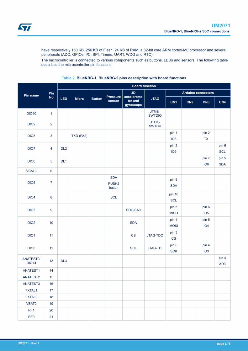
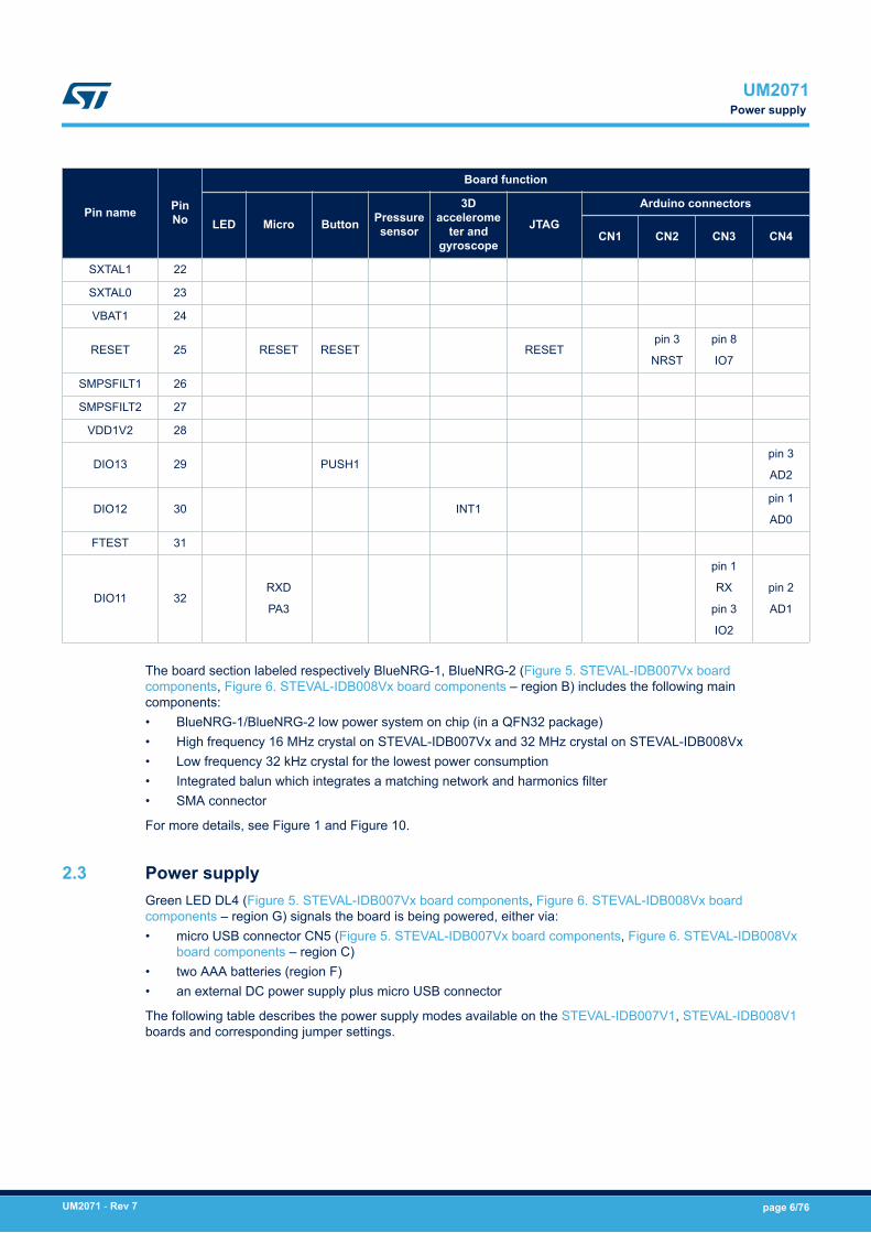
have respectively 160 KB, 256 KB of Flash, 24 KB of RAM, a 32-bit core ARM cortex-M0 processor and severalperipherals (ADC, GPIOs, I²C, SPI, Timers, UART, WDG and RTC).The microcontroller is connected to various components such as buttons, LEDs and sensors. The following tabledescribes the microcontroller pin functions.
Table 2. BlueNRG-1, BlueNRG-2 pins description with board functions
Pin name PinNo
Board function
LED Micro Button Pressuresensor
3Daccelerome
ter andgyroscope
JTAG
Arduino connectors
CN1 CN2 CN3 CN4
DIO10 1 JTMS-SWTDIO
DIO9 2 JTCK-SWTCK
DIO8 3 TXD (PA2)pin 1
IO8
pin 2
TX
DIO7 4 DL2pin 2
IO9
pin 6
SCL
DIO6 5 DL1pin 7
IO6
pin 5
SDA
VBAT3 6
DIO5 7SDA
PUSH2button
pin 9
SDA
DIO4 8 SCLpin 10
SCL
DIO3 9 SDO/SA0pin 5
MISO
pin 6
IO5
DIO2 10 SDApin 4
MOSI
pin 5
IO4
DIO1 11 CS JTAG-TDOpin 3
CS
DIO0 12 SCL JTAG-TDIpin 6
SCK
pin 4
IO3
ANATEST0/DIO14 13 DL3
pin 4
AD3
ANATEST1 14
ANATEST2 15
ANATEST3 16
FXTAL1 17
FXTAL0 18
VBAT2 19
RF1 20
RF0 21
UM2071BlueNRG-1, BlueNRG-2 SoC connections
UM2071 - Rev 7 page 5/76
Pin name PinNo
Board function
LED Micro Button Pressuresensor
3Daccelerome
ter andgyroscope
JTAG
Arduino connectors
CN1 CN2 CN3 CN4
SXTAL1 22
SXTAL0 23
VBAT1 24
RESET 25 RESET RESET RESETpin 3
NRST
pin 8
IO7
SMPSFILT1 26
SMPSFILT2 27
VDD1V2 28
DIO13 29 PUSH1pin 3
AD2
DIO12 30 INT1pin 1
AD0
FTEST 31
DIO11 32RXD
PA3
pin 1
RX
pin 3
IO2
pin 2
AD1
The board section labeled respectively BlueNRG-1, BlueNRG-2 (Figure 5. STEVAL-IDB007Vx boardcomponents, Figure 6. STEVAL-IDB008Vx board components – region B) includes the following maincomponents:• BlueNRG-1/BlueNRG-2 low power system on chip (in a QFN32 package)• High frequency 16 MHz crystal on STEVAL-IDB007Vx and 32 MHz crystal on STEVAL-IDB008Vx• Low frequency 32 kHz crystal for the lowest power consumption• Integrated balun which integrates a matching network and harmonics filter• SMA connector
For more details, see Figure 1 and Figure 10.
2.3 Power supplyGreen LED DL4 (Figure 5. STEVAL-IDB007Vx board components, Figure 6. STEVAL-IDB008Vx boardcomponents – region G) signals the board is being powered, either via:• micro USB connector CN5 (Figure 5. STEVAL-IDB007Vx board components, Figure 6. STEVAL-IDB008Vx
board components – region C)• two AAA batteries (region F)• an external DC power supply plus micro USB connector
The following table describes the power supply modes available on the STEVAL-IDB007V1, STEVAL-IDB008V1boards and corresponding jumper settings.
UM2071Power supply
UM2071 - Rev 7 page 6/76
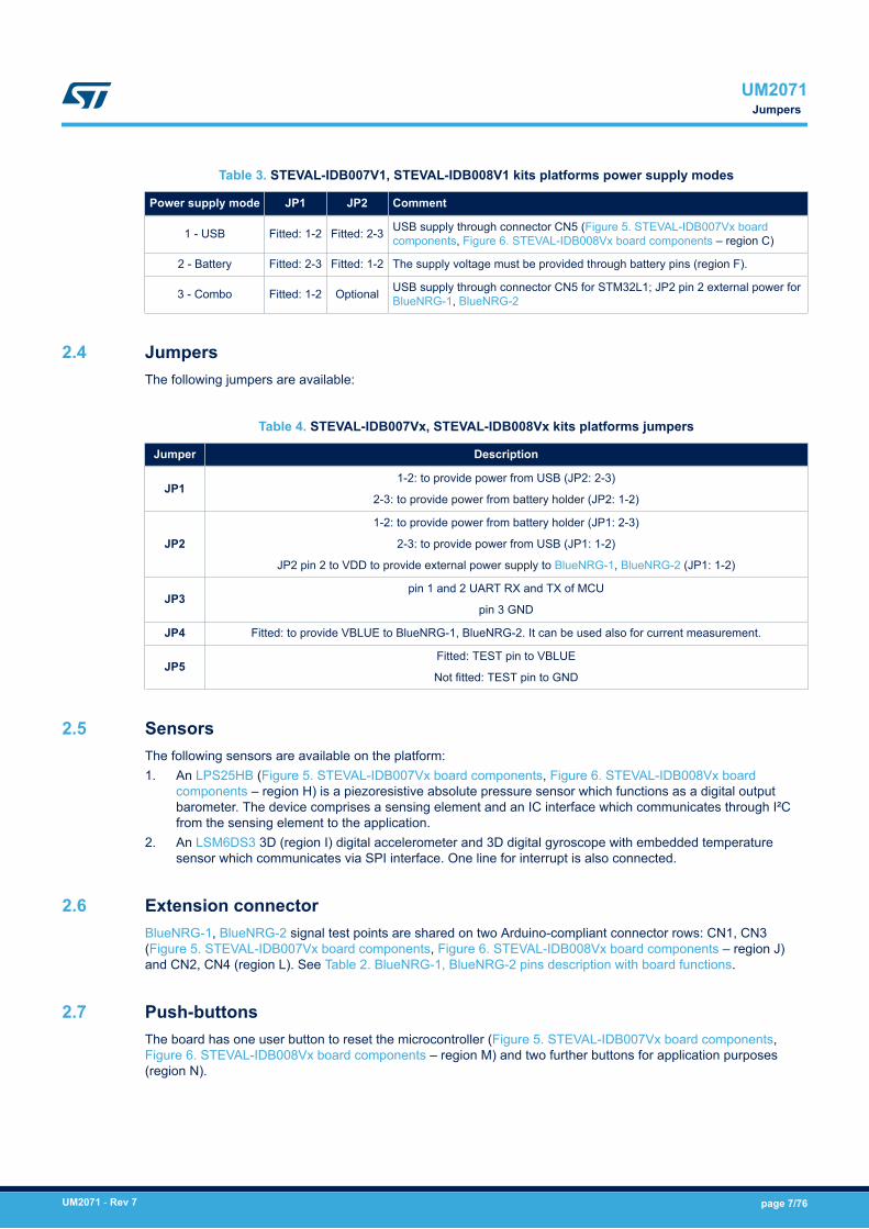
Table 3. STEVAL-IDB007V1, STEVAL-IDB008V1 kits platforms power supply modes
Power supply mode JP1 JP2 Comment
1 - USB Fitted: 1-2 Fitted: 2-3 USB supply through connector CN5 (Figure 5. STEVAL-IDB007Vx boardcomponents, Figure 6. STEVAL-IDB008Vx board components – region C)
2 - Battery Fitted: 2-3 Fitted: 1-2 The supply voltage must be provided through battery pins (region F).
3 - Combo Fitted: 1-2 Optional USB supply through connector CN5 for STM32L1; JP2 pin 2 external power forBlueNRG-1, BlueNRG-2
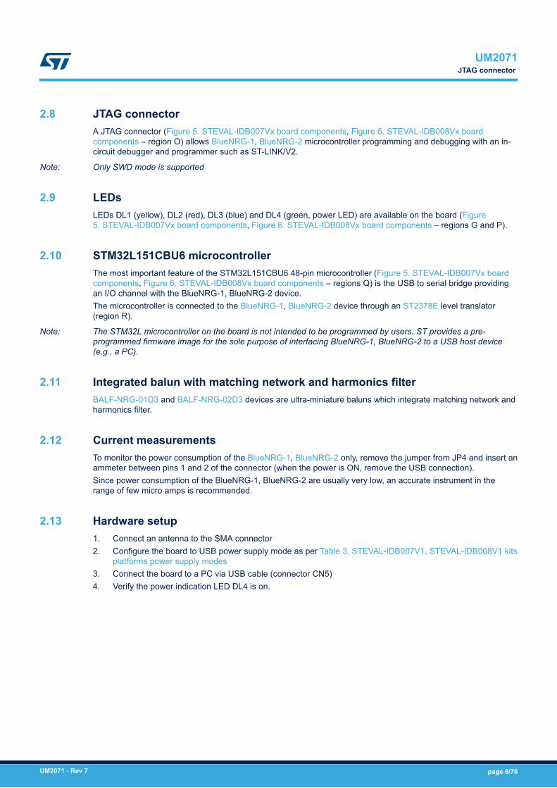
2.4 JumpersThe following jumpers are available:
Table 4. STEVAL-IDB007Vx, STEVAL-IDB008Vx kits platforms jumpers
Jumper Description
JP11-2: to provide power from USB (JP2: 2-3)
2-3: to provide power from battery holder (JP2: 1-2)
JP2
1-2: to provide power from battery holder (JP1: 2-3)
2-3: to provide power from USB (JP1: 1-2)
JP2 pin 2 to VDD to provide external power supply to BlueNRG-1, BlueNRG-2 (JP1: 1-2)
JP3pin 1 and 2 UART RX and TX of MCU
pin 3 GND
JP4 Fitted: to provide VBLUE to BlueNRG-1, BlueNRG-2. It can be used also for current measurement.
JP5Fitted: TEST pin to VBLUE
Not fitted: TEST pin to GND
2.5 SensorsThe following sensors are available on the platform:1. An LPS25HB (Figure 5. STEVAL-IDB007Vx board components, Figure 6. STEVAL-IDB008Vx board
components – region H) is a piezoresistive absolute pressure sensor which functions as a digital outputbarometer. The device comprises a sensing element and an IC interface which communicates through I²Cfrom the sensing element to the application.
2. An LSM6DS3 3D (region I) digital accelerometer and 3D digital gyroscope with embedded temperaturesensor which communicates via SPI interface. One line for interrupt is also connected.
2.6 Extension connectorBlueNRG-1, BlueNRG-2 signal test points are shared on two Arduino-compliant connector rows: CN1, CN3(Figure 5. STEVAL-IDB007Vx board components, Figure 6. STEVAL-IDB008Vx board components – region J)and CN2, CN4 (region L). See Table 2. BlueNRG-1, BlueNRG-2 pins description with board functions.
2.7 Push-buttonsThe board has one user button to reset the microcontroller (Figure 5. STEVAL-IDB007Vx board components,Figure 6. STEVAL-IDB008Vx board components – region M) and two further buttons for application purposes(region N).
UM2071 Jumpers
UM2071 - Rev 7 page 7/76
2.8 JTAG connectorA JTAG connector (Figure 5. STEVAL-IDB007Vx board components, Figure 6. STEVAL-IDB008Vx boardcomponents – region O) allows BlueNRG-1, BlueNRG-2 microcontroller programming and debugging with an in-circuit debugger and programmer such as ST-LINK/V2.
Note: Only SWD mode is supported
2.9 LEDsLEDs DL1 (yellow), DL2 (red), DL3 (blue) and DL4 (green, power LED) are available on the board (Figure5. STEVAL-IDB007Vx board components, Figure 6. STEVAL-IDB008Vx board components – regions G and P).
2.10 STM32L151CBU6 microcontrollerThe most important feature of the STM32L151CBU6 48-pin microcontroller (Figure 5. STEVAL-IDB007Vx boardcomponents, Figure 6. STEVAL-IDB008Vx board components – regions Q) is the USB to serial bridge providingan I/O channel with the BlueNRG-1, BlueNRG-2 device.The microcontroller is connected to the BlueNRG-1, BlueNRG-2 device through an ST2378E level translator(region R).
Note: The STM32L microcontroller on the board is not intended to be programmed by users. ST provides a pre-programmed firmware image for the sole purpose of interfacing BlueNRG-1, BlueNRG-2 to a USB host device(e.g., a PC).
2.11 Integrated balun with matching network and harmonics filterBALF-NRG-01D3 and BALF-NRG-02D3 devices are ultra-miniature baluns which integrate matching network andharmonics filter.
2.12 Current measurementsTo monitor the power consumption of the BlueNRG-1, BlueNRG-2 only, remove the jumper from JP4 and insert anammeter between pins 1 and 2 of the connector (when the power is ON, remove the USB connection).Since power consumption of the BlueNRG-1, BlueNRG-2 are usually very low, an accurate instrument in therange of few micro amps is recommended.
2.13 Hardware setup1. Connect an antenna to the SMA connector2. Configure the board to USB power supply mode as per Table 3. STEVAL-IDB007V1, STEVAL-IDB008V1 kits
platforms power supply modes3. Connect the board to a PC via USB cable (connector CN5)4. Verify the power indication LED DL4 is on.
UM2071JTAG connector
UM2071 - Rev 7 page 8/76

3 BlueNRG-1, BlueNRG-2 Navigator
BlueNRG-1, BlueNRG-2 Navigator are user friendly GUI which lets you select and run demonstration applicationseasily, without requiring any extra hardware. With it, you can access the following DK software packagecomponents:• BlueNRG-1, BlueNRG-2 Bluetooth low energy (BLE) demonstration applications• BlueNRG-1, BlueNRG-2 peripheral driver examples• BlueNRG-1, BlueNRG-2 2.4 GHz radio proprietary examples• BlueNRG-1, BlueNRG-2 development kits• release notes• license files
With BlueNRG-1 DK Navigator, you can directly download and run the selected prebuilt application binary image(BLE examples or peripheral driver example) on the BlueNRG-1, BlueNRG-2 platform without a JTAG interface.The interface gives demo descriptions and access to board configurations and source code if needed.User can run the utility through the BlueNRG-1 and BlueNRG-2 Navigator icon under:Start → STMicroelectronics → BlueNRG -1_2 DK X.X.X → BlueNRG-1 Navigator, BlueNRG-2 Navigator or Start→ STMicroelectronics → BlueNRG -1_V1 DK X.X.X → BlueNRG-1 Navigator.
Figure 7. BlueNRG-1 Navigator
Note: BlueNRG-1 Navigator and BlueNRG-2 Navigator are two instances of the same application tailored for thespecific selected device, in order to select the related available resources. Next sections focus on BlueNRG-1Navigator, but same concepts are also valid for BlueNRG-2 Navigator.
3.1 BlueNRG-1 Navigator ‘Demonstration Applications’You can navigate the menus for the reference/demo application you want to launch. For each application, thefollowing information is provided:• Application settings (if applicable)• Application description• Application hardware related information (e.g., LED signals, jumper configurations, etc.)
The following functions are also available for each application:
UM2071BlueNRG-1, BlueNRG-2 Navigator
UM2071 - Rev 7 page 9/76
• Flash: to automatically download and run the available prebuilt binary file to a BlueNRG-1 platformconnected to a PC USB port.
• Doc: to display application documentation (html format)• Project: to open the project folder with application headers, source and project files.
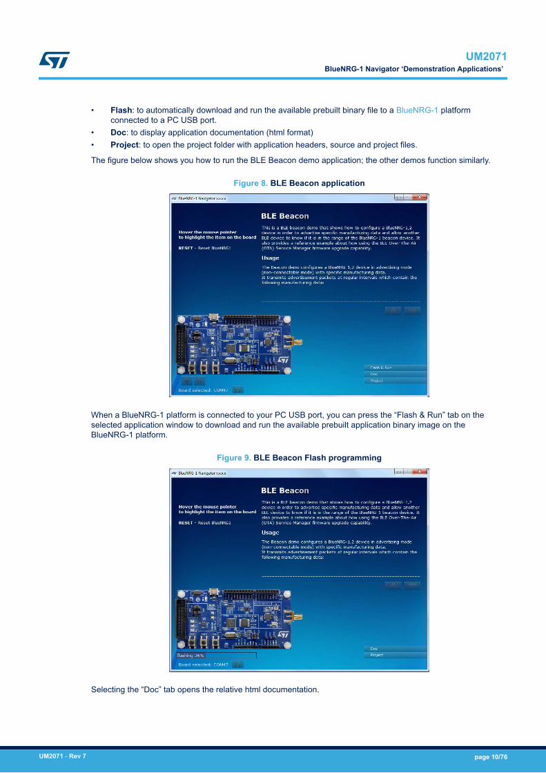
The figure below shows you how to run the BLE Beacon demo application; the other demos function similarly.
Figure 8. BLE Beacon application
When a BlueNRG-1 platform is connected to your PC USB port, you can press the “Flash & Run” tab on theselected application window to download and run the available prebuilt application binary image on theBlueNRG-1 platform.
Figure 9. BLE Beacon Flash programming
Selecting the “Doc” tab opens the relative html documentation.
UM2071BlueNRG-1 Navigator ‘Demonstration Applications’
UM2071 - Rev 7 page 10/76
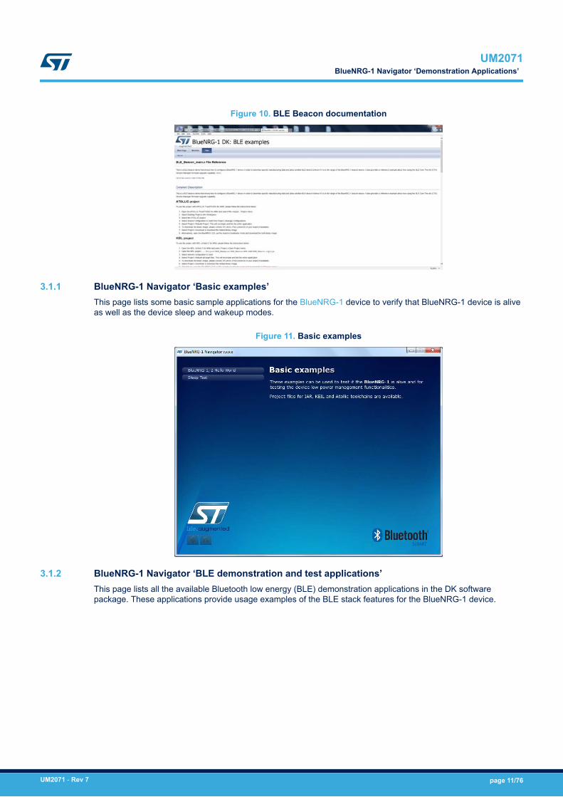
Figure 10. BLE Beacon documentation
3.1.1 BlueNRG-1 Navigator ‘Basic examples’This page lists some basic sample applications for the BlueNRG-1 device to verify that BlueNRG-1 device is aliveas well as the device sleep and wakeup modes.
Figure 11. Basic examples
3.1.2 BlueNRG-1 Navigator ‘BLE demonstration and test applications’This page lists all the available Bluetooth low energy (BLE) demonstration applications in the DK softwarepackage. These applications provide usage examples of the BLE stack features for the BlueNRG-1 device.
UM2071BlueNRG-1 Navigator ‘Demonstration Applications’
UM2071 - Rev 7 page 11/76
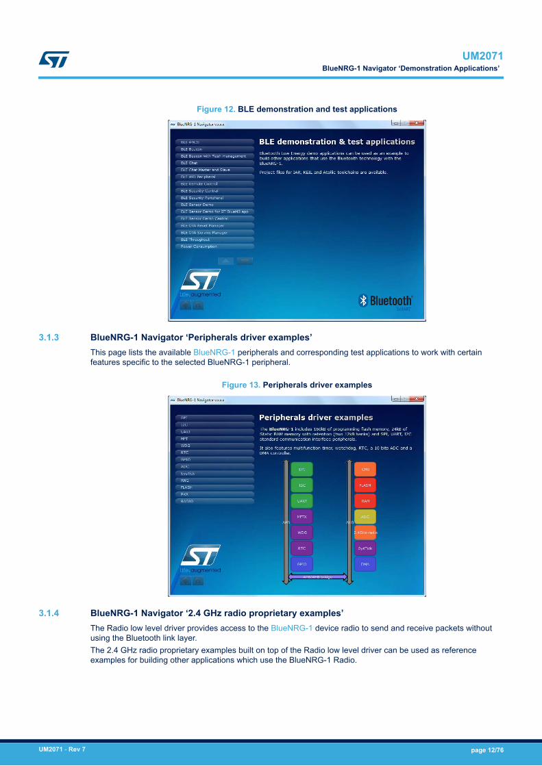
Figure 12. BLE demonstration and test applications
3.1.3 BlueNRG-1 Navigator ‘Peripherals driver examples’This page lists the available BlueNRG-1 peripherals and corresponding test applications to work with certainfeatures specific to the selected BlueNRG-1 peripheral.
Figure 13. Peripherals driver examples
3.1.4 BlueNRG-1 Navigator ‘2.4 GHz radio proprietary examples’The Radio low level driver provides access to the BlueNRG-1 device radio to send and receive packets withoutusing the Bluetooth link layer.The 2.4 GHz radio proprietary examples built on top of the Radio low level driver can be used as referenceexamples for building other applications which use the BlueNRG-1 Radio.
UM2071BlueNRG-1 Navigator ‘Demonstration Applications’
UM2071 - Rev 7 page 12/76
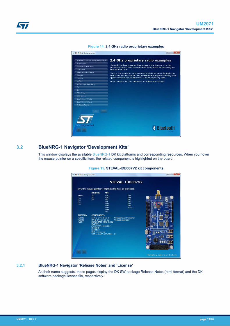
Figure 14. 2.4 GHz radio proprietary examples
3.2 BlueNRG-1 Navigator ‘Development Kits’This window displays the available BlueNRG-1 DK kit platforms and corresponding resources. When you hoverthe mouse pointer on a specific item, the related component is highlighted on the board.
Figure 15. STEVAL-IDB007V2 kit components
3.2.1 BlueNRG-1 Navigator ‘Release Notes’ and ‘License’As their name suggests, these pages display the DK SW package Release Notes (html format) and the DKsoftware package license file, respectively.
UM2071BlueNRG-1 Navigator ‘Development Kits’
UM2071 - Rev 7 page 13/76
4 BlueNRG-1 radio parameters wizard
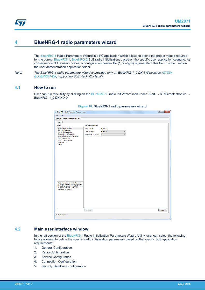
The BlueNRG-1 Radio Parameters Wizard is a PC application which allows to define the proper values requiredfor the correct BlueNRG-1, BlueNRG-2 BLE radio initialization, based on the specific user application scenario. Asconsequence of the user choices, a configuration header file (*_config.h) is generated: this file must be used onthe user demonstration application folder.
Note: The BlueNRG-1 radio parameters wizard is provided only on BlueNRG-1_2 DK SW package (STSW-BLUENRG1-DK) supporting BLE stack v2.x family.
4.1 How to runUser can run this utility by clicking on the BlueNRG-1 Radio Init Wizard icon under: Start → STMicroelectronics →BlueNRG -1_2 DK X.X.X
Figure 16. BlueNRG-1 radio parameters wizard
4.2 Main user interface windowIn the left section of the BlueNRG-1 Radio Initialization Parameters Wizard Utility, user can select the followingtopics allowing to define the specific radio initialization parameters based on the specific BLE applicationrequirements:1. General Configuration2. Radio Configuration3. Service Configuration4. Connection Configuration5. Security DataBase configuration
UM2071BlueNRG-1 radio parameters wizard
UM2071 - Rev 7 page 14/76
6. OTA configuration7. Privacy configuration8. Overview9. OutputRefer to the BlueNRG-1 Radio Parameters Wizard documentation available within BlueNRG-1_2 DK SW packagefor more details about each provided configuration section.
UM2071Main user interface window
UM2071 - Rev 7 page 15/76
5 Programming with BlueNRG-1, BlueNRG-2 system on chip
The BlueNRG-1, BlueNRG-2 Bluetooth low energy (BLE) stack is provided as a binary library. A set of APIs tocontrol BLE functionality. Some callbacks are also provided for user applications to handle BLE stack events. Theuser is simply requested to link this binary library to his or her application and use the relevant APIs to accessBLE functions and complete the stack event callbacks to manage responses according to applicationrequirements.A set of software driver APIs is also included for accessing the BlueNRG-1, BlueNRG-2 SoC peripherals andresources (ADC, GPIO, I²C, MFTX, Micro, RTC, SPI, SysTick, UART and WDG).The development kit software includes sample code demonstrating how to configure BlueNRG-1, BlueNRG-2 anduse the device peripherals and BLE APIs and event callbacks. Documentation on the BLE APIs, callbacks, andperipheral drivers are provided in separate documents.
5.1 Software directory structureThe BlueNRG-1, BlueNRG-2 DK software packages files are organized in the following main directories:• Application: containing BlueNRG-1, BlueNRG-2 Navigator and Radio Parameters Wizard PC applications.• Doc: with doxygen BLE APIs and events, BlueNRG-1, BlueNRG-2 peripheral drivers, BLE demo
applications, BlueNRG-1, BlueNRG-2 Peripheral examples, BlueNRG-1, BlueNRG-2 SDK and HAL driverdocumentation, DK release notes and license file.
• Firmware: with prebuilt binary BLE and peripheral driver sample applications.• Library
– Bluetooth LE: Bluetooth low energy stack binary library and all the definitions of stack APIs, stack andevents callbacks. BLE stack v2.1 or later configuration header and source files.
– BLE_Application: BLE application framework files (BLE stack layers define values, OTA FW upgrade,BLE utilities, master library).
– BlueNRG1_Periph_Driver: BlueNRG-1, BlueNRG-2 drivers for device peripherals (ADC, clock, DMA,Flash, GPIO, I²C, timers, RTC, SPI, UARR and watchdog).
– CMSIS: BlueNRG-1 CMSIS files.– SDK_Eval_BlueNRG1: SDK drivers providing an API interface to the BlueNRG-1, BlueNRG-2 platform
hardware resources (LEDs, buttons, sensors, I/O channel).– HAL: Hardware abstraction level APIs for abstracting certain BlueNRG-1 hardware features (sleep
modes, clock based on SysTick, etc.).• Project
– BLE_Examples: Bluetooth low energy demonstration application including Headers, source files andEWARM, Keil and Atollic project files.
– BlueNRG1_Periph_Examples: with sample applications for the BlueNRG-1, BlueNRG-2 peripheralsand hardware resources, including Headers, source files and project files.
• Utility: contains some utilities
Note: The selection between BlueNRG-1, BlueNRG-2 device is done at compile time using a specific define valueBLUENRG2_DEVICE for selecting BlueNRG-2 device. Default configuration (no define value) selectsBlueNRG-1 device.
Note: BlueNRG-1_V1 DK SW package framework refers only BlueNRG-1 device.
Note: BLE_Application folder is available only on BlueNRG-1_2 DK SW package v3.0.0 or later.
UM2071Programming with BlueNRG-1, BlueNRG-2 system on chip
UM2071 - Rev 7 page 16/76
6 BLE beacon demonstration application
The BLE beacon demo is supported by the BlueNRG-1, BlueNRG-2 development platforms (STEVAL-IDB007Vx,STEVAL-IDB008Vx). It demonstrates how to configure a BlueNRG-1 device to advertise specific manufacturingdata and allow another BLE device to determine whether it is in BLE beacon device range.
6.1 BLE Beacon application setupThis section describes how to configure a BLE device to act as a beacon device.
6.1.1 InitializationThe BLE stack must be correctly initialized thus:
aci_gatt_init();aci_gap_init(GAP_PERIPHERAL_ROLE, 0, 0x08, &service_handle, &dev_name_char_handle,&appearance_char_handle);
See the BLE stack documentation for more information on these and following commands.
6.1.2 Define advertising dataThe BLE Beacon application advertises the following manufacturing data:
Table 5. BlueNRG-1 Beacon advertising manufacturing data
Data field Description Notes
Company identifier code SIG company identifier (1) Default is 0x0030 (STMicroelectronics)
ID Beacon ID Fixed value
Location UUID Beacons UUID Used to distinguish specific beacons from others
Major number Identifier for a group of beacons Used to group a related set of beacons
Minor number Identifier for a single beacon Used to identify a single beacon
Tx Power 2's complement of the Tx power Used to establish how far you are from device
1. available at: https://www.bluetooth.org/en-us/specification/assigned-numbers/company-identifiers
6.1.3 Entering non-connectable modeThe BLE Beacon device uses the GAP API command to enter non-connectable mode thus:
aci_gap_set_discoverable(ADV_NONCONN_IND, 160, 160, PUBLIC_ADDR,NO_WHITE_LIST_USE,0, NULL, 0, NULL, 0, 0);
To advertise the specific selected manufacturer data, the BLE Beacon application can use the following GAPAPIs:
/* Remove TX power level field from the advertising data: it is necessary to haveenough space for the beacon manufacturing data */aci_gap_delete_ad_type(AD_TYPE_TX_POWER_LEVEL);/* Define the beacon manufacturing payload */uint8_t manuf_data[] = {26, AD_TYPE_MANUFACTURER_SPECIFIC_DATA, 0x30, 0x00,//Company identifier code (Default is 0x0030 - STMicroelectronics) 0x02,// ID0x15,//Length of the remaining payload0xE2, 0x0A, 0x39, 0xF4, 0x73, 0xF5, 0x4B, 0xC4, //Location UUID0xA1, 0x2F, 0x17, 0xD1, 0xAD, 0x07, 0xA9, 0x61,0x00, 0x02, // Major number
UM2071 BLE beacon demonstration application
UM2071 - Rev 7 page 17/76
0x00, 0x02, // Minor number0xC8//2's complement of the Tx power (-56dB)};};/* Set the beacon manufacturing data on the advertising packet */ aci_gap_update_adv_data(27, manuf_data);
Note: BLE Beacon with Flash Management demonstration application is also available. It allows to configure a Beacondevice as with the original Beacon demo application; it also shows how to properly handle Flash operations(Erase and Write) and preserve the BLE radio activities. This is achieved by synchronizing Flash operations withthe scheduled BLE radio activities through the aci_hal_end_of_radio_activity_event() event callback timinginformation.
UM2071 BLE Beacon application setup
UM2071 - Rev 7 page 18/76
7 BLE chat demo application
The BLE chat demo (server and client roles) is supported on the BlueNRG-1, BlueNRG-2 development platforms(STEVAL-IDB007Vx, STEVAL-IDB008Vx). It implements simple two-way communication between two BLEdevices, demonstrating point-to-point wireless communication using the BlueNRG-1 product.This demo application exposes a single chat service with the following (20 byte max.) characteristic values:• The TX characteristic, with which the client can enable notifications; when the server has data to be sent, it
sends notifications with the value of the TX characteristic.• The RX characteristic, is a writable characteristic; when the client has data to be sent to the server, it writes
a value in this characteristic.
There are two device roles which can be selected through the specific project workspace:• The Server that exposes the chat service (BLE peripheral device).• The Client that uses the chat service (BLE central device).
The application requires two devices to be programmed with respective server and client roles. These must beconnected to a PC via USB with an open serial terminal for each device, with the following configurations:
Table 6. Serial port configuration
Parameter Value
Baudrate 115200 bit/s
Data bits 8
Parity bits None
Stop bits 1
The application listens for keys typed in one device terminal and sends them to the remote device when the returnkey is pressed; the remote device then outputs the received RF messages to the serial port. Therefore, anythingtyped in one terminal becomes visible in the other.
7.1 Peripheral and central device setupThis section describes how two BLE chat devices (server-peripheral and client-central) interact with each other toset up a point-to-point wireless chat.BLE device must first be set up on both devices by sending a series of API commands to the processor.
7.1.1 InitializationThe BLE stack must be correctly initialized before establishing a connection with another BLE device. This isdone with aci_gatt_init() and aci_gap_init() APIs:
aci_gatt_init();
BLE Chat server role:
aci_gap_init(GAP_PERIPHERAL_ROLE, 0, 0x08, &service_handle, &dev_name_char_handle,&appearance_char_handle);
BLE Chat client role:
aci_gap_init(GAP_CENTRAL_ROLE, 0, 0x08, &service_handle, &dev_name_char_handle, &appearance_char_handle);
UM2071BLE chat demo application
UM2071 - Rev 7 page 19/76
Peripheral and central BLE roles must be specified in the aci_gap_init() command. See the BLE stack APIdocumentation for more information on these and following commands.
7.1.2 Add service and characteristicsThe chat service is added to the BLE chat server device via:
aci_gatt_add_service(UUID_TYPE_128, &service_uuid, PRIMARY_SERVICE, 7,&chatServHandle);
Where service_uuid is the private service 128-bit UUID allocated for the chat service (Primary service). Thecommand returns the service handle in chatServHandle. The TX characteristic is added using the followingcommand on the BLE Chat server device:
aci_gatt_add_char(chatServHandle, UUID_TYPE_128, &charUuidTX, 20, CHAR_PROP_NOTIFY, ATTR_PERMISSION_NONE, 0, 16, 1, &TXCharHandle);
Where charUuidTX is the private characteristic 128-bit UUID allocated for the TX characteristic (notify property).The characteristic handle is returned on the TXCharHandle variable.The RX characteristic is added using the following command on the BLE Chat server device:
aci_gatt_add_char(chatServHandle, UUID_TYPE_128, &charUuidRX, 20, CHAR_PROP_WRITE|CHAR_PROP_WRITE_WITHOUT_RESP, ATTR_PERMISSION_NONE, GATT_SERVER_ATTR_WRITE,16, 1,&RXCharHandle);
Where charUuidRX is the private characteristic 128-bit UUID allocated for the RX characteristic (write property).The characteristic handle is returned on the RXCharHandle variable.See the BLE stack API documentation for more information on these and following commands.
7.1.3 Enter connectable modeThe server device uses GAP API commands to enter the general discoverable mode:
aci_gap_set_discoverable(ADV_IND, 0, 0, PUBLIC_ADDR, NO_WHITE_LIST_USE,8,local_name, 0, NULL, 0, 0);
The local_name parameter contains the name presented in advertising data, as per Bluetooth core specificationversion 4.2, Vol. 3, Part C, Ch. 11.
7.1.4 Connection with central deviceOnce the server device is discoverable by the BLE chat client device, the client device usesaci_gap_create_connection()to connect with the BLE chat server device:
aci_gap_create_connection(0x4000, 0x4000, PUBLIC_ADDR, bdaddr, PUBLIC_ADDR, 40, 40, 0, 60, 2000 , 2000);
Where bdaddr is the peer address of the client device.Once the two devices are connected, you can set up corresponding serial terminals and type messages in eitherof them. The typed characters are stored in two respective buffers and when the return key is pressed:• on the BLE chat server device, the typed characters are sent to the BLE chat client device by notifying the
previously added TX characteristic (after notifications are enabled) with:
aci_gatt_update_char_value(chatServHandle,TXCharHandle,0,len, (uint8_t*)cmd+j);
• on the BLE chat client device, the typed characters are sent to the BLE chat server device by writing thepreviously added RX characteristic with:
UM2071 Peripheral and central device setup
UM2071 - Rev 7 page 20/76
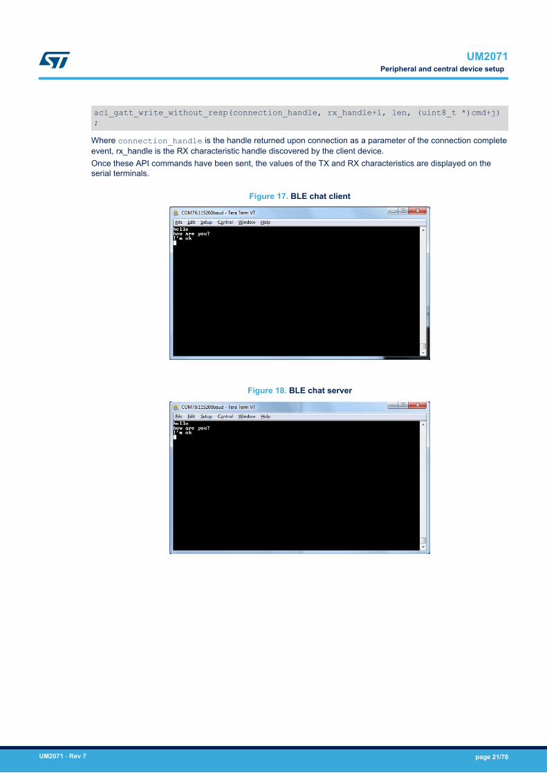
aci_gatt_write_without_resp(connection_handle, rx_handle+1, len, (uint8_t *)cmd+j);
Where connection_handle is the handle returned upon connection as a parameter of the connection completeevent, rx_handle is the RX characteristic handle discovered by the client device.Once these API commands have been sent, the values of the TX and RX characteristics are displayed on theserial terminals.
Figure 17. BLE chat client
Figure 18. BLE chat server
UM2071 Peripheral and central device setup
UM2071 - Rev 7 page 21/76
8 BLE chat master and slave demo application
The BLE chat master and slave demo is supported on the BlueNRG-1, BlueNRG-2development platforms(STEVAL-IDB007Vx, STEVAL-IDB008Vx). It demonstrates simple point-to-point wireless communication using asingle application which configures the chat client and server roles at runtime.The new chat demo application configures a BLE device as central or peripheral using the API:
aci_gap_init(GAP_CENTRAL_ROLE|GAP_PERIPHERAL_ROLE, 0, 0x07, &service_handle, &dev_name_char_handle, &appearance_char_handle);
It then initiates a discovery procedure for another BLE device configured with the same chat master and slaveapplication image.If such a device is found within a random interval, it starts a connection procedure and waits until a connection isestablished. If the discovery procedure time expires without finding another chat master and slave device, thedevice enters discovery mode and waits for another chat master and slave device to discover and connect to it.When connection is established, the client and server roles are defined and the chat communication channel canbe used.This demo application exposes a single chat service with the following (20 byte max.) characteristic values:• The TX characteristic, with which the client can enable notifications; when the server has data to be sent, it
sends notifications with the value of the TX characteristic.• The RX characteristic, is a writable characteristic; when the client has data to be sent to the server, it writes
a value in this characteristic.
The application requires two devices to be programmed with the same application, with the server and client rolesdefined at runtime. Connect the two devices to a PC via USB and open a serial terminal on both with the sameconfiguration as Table 6. Serial port configuration.The application listens for keys typed in one device terminal and sends them to the remote device when the returnkey is pressed; the remote device then outputs the received RF messages to the serial port. Therefore, anythingtyped in one terminal becomes visible in the other.
8.1 BLE chat master and slave rolesThis section describes how two BLE chat master and slave devices interact with each other in order to set up apoint-to-point wireless chat.The BLE stack must first be set up on both devices by sending a series of API commands to the processor. Thechat master and slave client and server roles are defined at runtime.
8.1.1 InitializationThe BLE stack must be correctly initialized before establishing a connection with another BLE device. This isdone with two commands:
aci_gatt_init();
aci_gap_init(GAP_CENTRAL_ROLE|GAP_PERIPHERAL_ROLE, TRUE,0x07, &service_handle, &dev_name_char_handle, &appearance_char_handle);
The BLE peripheral and central roles are specified in the aci_gap_init() command. See the BLE APIdocumentation for more information on these and following commands.
8.1.2 Add service and characteristicsRefer to Section 7.1.2 Add service and characteristics .
8.1.3 Start discovery procedureTo find another BLE chat master and slave device in discovery mode, a discovery procedure must be started via:
UM2071BLE chat master and slave demo application
UM2071 - Rev 7 page 22/76
aci_gap_start_general_discovery_proc(0x4000, 0x4000, 0x00, 0x00);
8.1.4 Enter connectable modeThe following GAP API command is used for entering general discoverable mode:
aci_gap_set_discoverable(ADV_IND, 0x90, 0x90, PUBLIC_ADDR, NO_WHITE_LIST_USE, sizeof(local_name), local_name, 0, NULL, 0x6, 0x8);
8.1.5 Connection with chat master and slave client deviceIn the above mentioned discovery and mode assignment procedures, the two chat master and slave applicationsassume respective client and server roles at runtime. During this initial configuration phase, when a chat masterand slave device is placed in discoverable mode and it is found by the other chat master and slave deviceperforming a discovery procedure, a Bluetooth low energy connection is created and the device roles are defined.The following GAP API command is used for connecting to the discovered device:
aci_gap_create_connection(0x4000, 0x4000,device_found_address_type, device_found_address, PUBLIC_ADDR, 40, 40, 0, 60, 2000 , 2000);
Where device_found_address_type is the address type of the discovered chat master and slave anddevice_found_address is the peer address of the discovered chat master and slave device.Once the two devices are connected, you can set up corresponding serial terminals and type messages in eitherof them. The typed characters are stored in two respective buffers and when the return key is pressed:On the BLE chat master-and-slave server device, the typed characters are sent to the master-and-slave clientdevice by notifying the previously added TX characteristic (after notifications have been enabled). This is donevia:
aci_gatt_update_char_value(chatServHandle, TXCharHandle, 0, len, (uint8_t *)cmd+j);
On the master-and-slave client device, the typed characters are sent to the master-and-slave server device, bywriting the previously added RX characteristic. This is done via:
aci_gatt_write_without_resp (connection_handle, rx_handle +1, len, (uint8_t *)cmd+j);
Where connection_handle is the handle returned upon connection as a parameter of the connection completeevent, rx_handle is the RX characteristic handle discovered by the client device.Once these API commands have been sent, the values of the TX and RX characteristics are displayed on theserial terminals.
UM2071BLE chat master and slave roles
UM2071 - Rev 7 page 23/76
9 BLE remote control demo application
The BLE remote control application is supported on the BlueNRG-1, BlueNRG-2 development platforms(STEVAL-IDB007Vx, STEVAL-IDB008Vx). It demonstrates how to control a remote device (like an actuator) usinga BlueNRG-1, BlueNRG-2 device.This application periodically broadcasts temperature values that can be read by any device. The data isencapsulated in a manufacturer-specific AD type and the content (besides the manufacturer ID, i.e., 0x0030 forSTMicroelectronics) is as follows:
Table 7. BLE remote advertising data
Byte 0 Byte 1 Byte2
App ID (0x05) Temperature value (little-endian)
The temperature value is given in tenths of degrees Celsius.The device is also connectable and exposes a characteristic used to control LEDs DL1 and DL3 on the BLE kitplatform. The value of this characteristic is a bitmap of 1 byte. Each bit controls one of the LEDs:• bit 0 is the status of LED DL1• bit 2 is the status of LED DL3.
A remote device can therefore connect and write this byte to change or read the status of these LEDs (1 for LEDON, 0 for LED OFF).The peripheral disconnects after a timeout (DISCONNECT_TIMEOUT) to prevent a central device remainingconnected to the device indefinitely.Security is not enabled by default, but this can be changed with ENABLE_SECURITY (refer to fileBLE_RC_main.h). When security is enabled, the central device must be authenticated before reading or writingthe device characteristic.To interact with a device configured as a BLE remote control, another BLE device (a BlueNRG-1, BlueNRG-2 orany Bluetooth® smart ready device) can be used to detect and view broadcast data.To control one of the LEDs, the device has to connect to a BlueNRG-1 BLE remote control device and write in theexposed control point characteristic. The Service UUID is ed0ef62e-9b0d-11e4-89d3-123b93f75cba. The controlpoint characteristic UUID is ed0efb1a-9b0d-11e4-89d3-123b93f75cba.
9.1 BLE remote control application setupThis section describes how to configure a BlueNRG-1 device to acting as a remote control device.
9.1.1 InitializationThe BLE stack must be correctly initialized before establishing a connection with another Bluetooth LE device.This is done with two commands:
aci_gatt_init();aci_gap_init(GAP_PERIPHERAL_ROLE, 0, 0x07, &service_handle, &dev_name_char_handle,&appearance_char_handle);
See BLE stack API documentation for more information on these and following commands.
9.1.2 Define advertising dataThe BLE remote control application advertises certain manufacturing data as follows:
/* Set advertising device name as Node */const uint8_t scan_resp_data[] = {0x05,AD_TYPE_COMPLETE_LOCAL_NAME,'N','o','d','e'
UM2071BLE remote control demo application
UM2071 - Rev 7 page 24/76
}/* Set scan response data */ hci_le_set_scan_response_data(sizeof(scan_resp_data),scan_resp_data);/* Set Undirected Connectable Mode */aci_gap_set_discoverable(ADV_IND, (ADV_INTERVAL_MIN_MS*1000)/625,(ADV_INTERVAL_MAX_MS*1000)/625, PUBLIC_ADDR, NO_WHITE_LIST_USE, 0, NULL, 0, NULL,0, 0);/* Set advertising data */hci_le_set_advertising_data(sizeof(adv_data),adv_data);
On the development platform, the temperature sensor value is set in the adv_data variable.
9.1.3 Add service and characteristicsThe BLE Remote Control service is added via:
aci_gatt_add_service(UUID_TYPE_128, &service_uuid, PRIMARY_SERVICE, 7,&RCServHandle);
Where service_uuid is the private service 128-bit UUID allocated for the BLE remote service(ed0ef62e-9b0d-11e4-89d3-123b93f75cba).The command returns the service handle in RCServHandle.The BLE remote control characteristic is added using the following command:
#if ENABLE_SECURITYaci_gatt_add_char(RCServHandle, UUID_TYPE_128, &controlPointUuid, 1,CHAR_PROP_READ|CHAR_PROP_WRITE|CHAR_PROP_WRITE_WITHOUT_RESP|CH AR_PROP_SIGNED_WRITE,ATTR_PERMISSION_AUTHEN_READ|ATTR_PERMISSION_AUTHEN_WRITE, GATT_NOTIFY_ATTRIBUTE_WRITE,16,1,&controlPointHandle);#elseaci_gatt_add_char(RCServHandle, UUID_TYPE_128, &controlPointUuid, 1,CHAR_PROP_READ|CHAR_PROP_WRITE|CHAR_PROP_WRITE_WITHOUT_RESP, ATTR_PERMISSION_NONE,GATT_NOTIFY_ATTRIBUTE_WRITE, 16,
1,&controlPointHandle);#endif
Where controlPointUuid is the private characteristic 128-bit UUID allocated for BLE remote controlcharacteristic (ed0efb1a-9b0d-11e4-89d3-123b93f75cba) and controlPointHandle is the BLE remote controlcharacteristic handle.If security is enabled, the characteristic properties must be set accordingly to enable authentication oncontrolPointUuid characteristic read and write.
9.1.4 Connection with a BLE Central deviceWhen connected to a BLE central device (another BlueNRG-1, BlueNRG-2 device or any Bluetooth® smart readydevice), the controlPointUuid characteristic is used to control the BLE remote control platform LED. Eachtime a write operation is performed on controlPointUuid, the aci_gatt_attribute_modified_event()callback is raised and the selected LEDs are turned on or off.
UM2071
BLE remote control application setup
UM2071 - Rev 7 page 25/76
10 BLE sensor profile demo
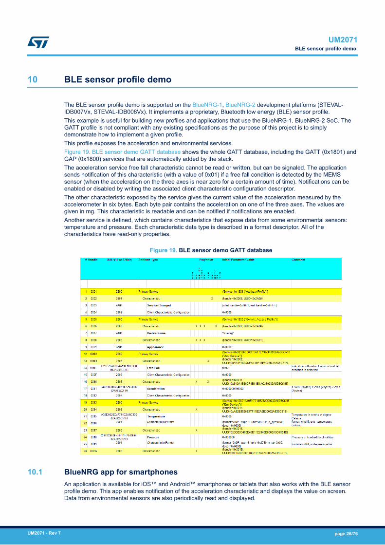
The BLE sensor profile demo is supported on the BlueNRG-1, BlueNRG-2 development platforms (STEVAL-IDB007Vx, STEVAL-IDB008Vx). It implements a proprietary, Bluetooth low energy (BLE) sensor profile.This example is useful for building new profiles and applications that use the BlueNRG-1, BlueNRG-2 SoC. TheGATT profile is not compliant with any existing specifications as the purpose of this project is to simplydemonstrate how to implement a given profile.This profile exposes the acceleration and environmental services.Figure 19. BLE sensor demo GATT database shows the whole GATT database, including the GATT (0x1801) andGAP (0x1800) services that are automatically added by the stack.The acceleration service free fall characteristic cannot be read or written, but can be signaled. The applicationsends notification of this characteristic (with a value of 0x01) if a free fall condition is detected by the MEMSsensor (when the acceleration on the three axes is near zero for a certain amount of time). Notifications can beenabled or disabled by writing the associated client characteristic configuration descriptor.The other characteristic exposed by the service gives the current value of the acceleration measured by theaccelerometer in six bytes. Each byte pair contains the acceleration on one of the three axes. The values aregiven in mg. This characteristic is readable and can be notified if notifications are enabled.Another service is defined, which contains characteristics that expose data from some environmental sensors:temperature and pressure. Each characteristic data type is described in a format descriptor. All of thecharacteristics have read-only properties.
Figure 19. BLE sensor demo GATT database
10.1 BlueNRG app for smartphonesAn application is available for iOS™ and Android™ smartphones or tablets that also works with the BLE sensorprofile demo. This app enables notification of the acceleration characteristic and displays the value on screen.Data from environmental sensors are also periodically read and displayed.
UM2071BLE sensor profile demo
UM2071 - Rev 7 page 26/76
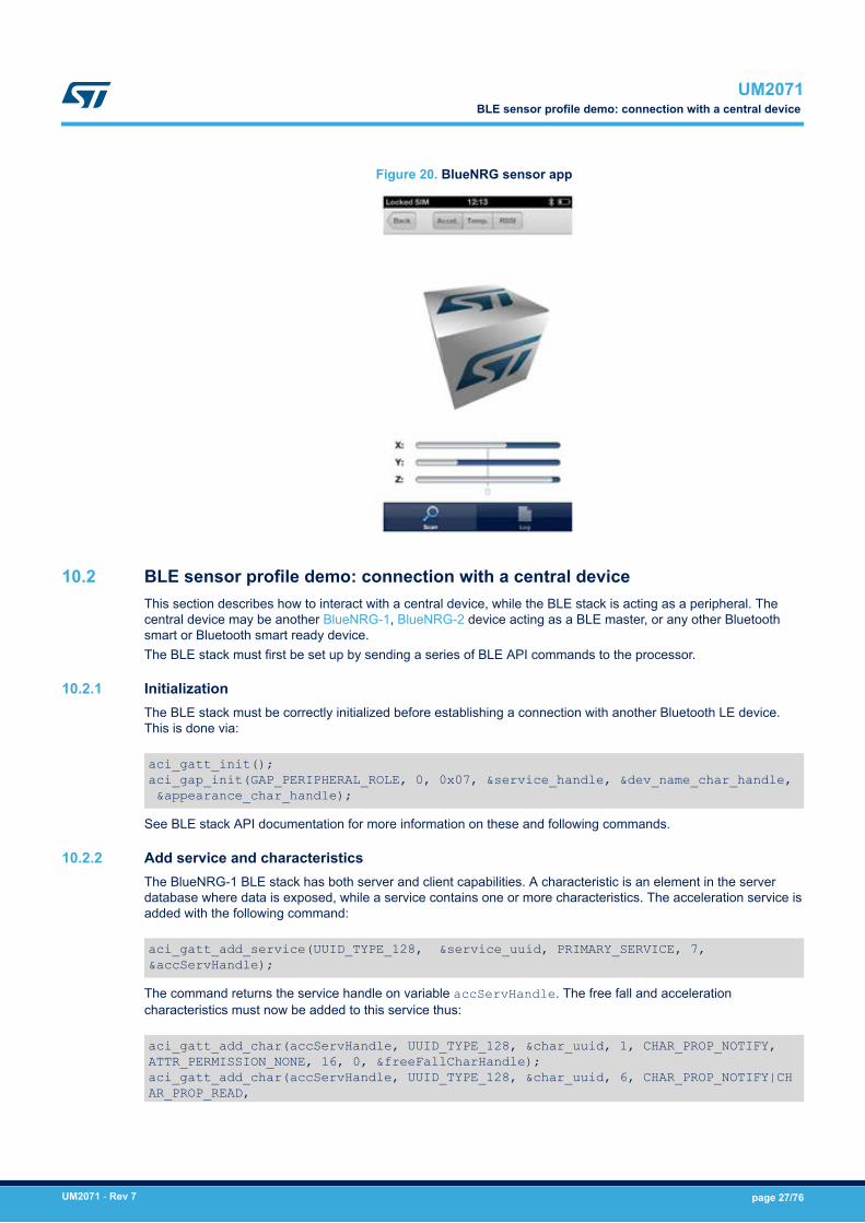
Figure 20. BlueNRG sensor app
10.2 BLE sensor profile demo: connection with a central deviceThis section describes how to interact with a central device, while the BLE stack is acting as a peripheral. Thecentral device may be another BlueNRG-1, BlueNRG-2 device acting as a BLE master, or any other Bluetoothsmart or Bluetooth smart ready device.The BLE stack must first be set up by sending a series of BLE API commands to the processor.
10.2.1 InitializationThe BLE stack must be correctly initialized before establishing a connection with another Bluetooth LE device.This is done via:
aci_gatt_init();aci_gap_init(GAP_PERIPHERAL_ROLE, 0, 0x07, &service_handle, &dev_name_char_handle,&appearance_char_handle);
See BLE stack API documentation for more information on these and following commands.
10.2.2 Add service and characteristicsThe BlueNRG-1 BLE stack has both server and client capabilities. A characteristic is an element in the serverdatabase where data is exposed, while a service contains one or more characteristics. The acceleration service isadded with the following command:
aci_gatt_add_service(UUID_TYPE_128, &service_uuid, PRIMARY_SERVICE, 7,&accServHandle);
The command returns the service handle on variable accServHandle. The free fall and accelerationcharacteristics must now be added to this service thus:
aci_gatt_add_char(accServHandle, UUID_TYPE_128, &char_uuid, 1, CHAR_PROP_NOTIFY,ATTR_PERMISSION_NONE, 16, 0, &freeFallCharHandle);aci_gatt_add_char(accServHandle, UUID_TYPE_128, &char_uuid, 6, CHAR_PROP_NOTIFY|CHAR_PROP_READ,
UM2071BLE sensor profile demo: connection with a central device
UM2071 - Rev 7 page 27/76
ATTR_PERMISSION_NONE, GATT_NOTIFY_READ_REQ_AND_WAIT_FOR_APPL_RESP, 16, 0, &accCharHandle);
The free fall and acceleration characteristics handles are returned on freeFallCharHandle andaccCharHandle variables respectively.Similar steps are followed for adding the environmental sensor and relative characteristics.
10.2.3 Enter connectable modeUse GAP API command to enter one of the discoverable and connectable modes:
aci_gap_set_discoverable(ADV_IND, (ADV_INTERVAL_MIN_MS*1000)/625,ADV_INTERVAL_MAX_MS*1000)/625, STATIC_RANDOM_ADDR, NO_WHITE_LIST_USE sizeof(local_name), local_name, 0, NULL, 0, 0);
Where
local_name[] = {AD_TYPE_COMPLETE_LOCAL_NAME,'B','l','u','e','N','R','G'};
The local_name parameter contains the name presented in advertising data, as per Bluetooth core specificationversion, Vol. 3, Part C, Ch. 11.
10.2.4 Connection with central deviceOnce the BLE stack is placed in discoverable mode, it can be detected by a central device. The smartphone appdescribed in Section 10.1 BlueNRG app for smartphones is designed for interact with the sensor profile demos (italso supports the BlueNRG-1 device).Any Bluetooth smart or Bluetooth smart ready device like a smartphone can connect to the BLE sensor profiledemo.For example, the LightBlue application in Apple Store® connects iPhone® versions 4S/5 and above can connectto the sensor profile device. When you use the LightBlue application, detected devices appear on the screen withthe BlueNRG name. By tapping on the box to connect to the device, a list of all the available services is shown onthe screen; tapping a service shows the characteristics for that service.The acceleration characteristic can be notified using the following command:
aci_gatt_update_char_value(accServHandle, accCharHandle, 0, 6, buff);
Where buff is a variable containing the three axes acceleration values.Once this API command has been sent, the new value of the characteristic is displayed on the phone.
UM2071BLE sensor profile demo: connection with a central device
UM2071 - Rev 7 page 28/76
11 BLE sensor profile center demo
The BLE sensor profile central demo is supported on the BlueNRG-1, BlueNRG-2 development platforms(STEVAL-IDB007Vx, STEVAL-IDB008Vx). It implements a basic version of the BLE Sensor Profile Central rolewhich emulates the Sensor Demo applications available for smartphones (iOS and android).This application configures a BlueNRG-1, BlueNRG-2 device as a Sensor device, Central role which is able tofind, connect and properly configure the free fall, acceleration and environment sensors characteristics providedby a BLE development platform configured as a BLE Sensor device, Peripheral role (refer to Section 10 BLEsensor profile demo).This application uses a new set of APIs allowing to perform the following operations on a BlueNRG-1, BlueNRG-2Master/Central device:• Master Configuration Functions• Master Device Discovery Functions• Master Device Connection Functions• Master Discovery Services, Characteristics Functions• Master Data Exchange Functions• Master Security Functions• Master Common Services Functions
These APIs are provided through a binary library and they are fully documented on available doxygendocumentation within the DK SW package. The following master/central binary libraries are provided onBluetooth_LE\Profile_Framework_Central\library folder:• libmaster_library_bluenrg1.a for IAR, Keil and Atollic toolchains on STSW-BLUENRG1-DK SW package• master_library_bluenrg1.lib for Keil toolchain on STSW-BNRG_V1-DK SW package• libmaster_library_bluenrg1.a for IAR and Atollic toolchains on STSW-BNRG_V1-DK SW package
UM2071BLE sensor profile central demo
UM2071 - Rev 7 page 29/76
12 BLE HID/HOGP demonstration application
The BLE HID/HOGP demonstration applications are supported by the BlueNRG-1, BlueNRG-2developmentplatforms (STEVAL-IDB007Vx, STEVAL-IDB008Vx). It demonstrates a BLE device using the standard HID/HOGPBluetooth low energy application profile. Keyboard and mouse demo examples are provided.
12.1 BLE HID/HOGP mouse demonstration applicationThe BLE HID mouse application implements a basic HID mouse with two buttons compliant with the standardHID/HOGP BLE application profile.The HID mouse device is named ‘STMouse’ in the central device list.The mouse movements are provided by the 3D accelerometer and 3D gyroscope on the BLE developmentplatform.• The left button is the ‘PUSH1’ button.• The right button is the ‘PUSH2’ button
If the HID mouse is not used for two minutes, it closes the connection and enters deep sleep mode. This idleconnection timeout can be changed from the application. To exit deep sleep mode, press the left PUSH1 button orreset the platform.
12.2 BLE HID/HOGP keyboard demonstration applicationThe BLE HID keyboard application implements a basic HID keyboard compliant with the standard HID/HOGPBLE application profile.The HID mouse device is named ‘STKeyboard’ in the central device list.To successfully complete the bonding and pairing procedure, insert the PIN: 123456.To use the HID keyboard:• Connect the BLE development platform to a PC USB port• Open a HyperTerminal window (115200, 8, N,1)• Put the cursor focus on the HyperTerminal window• The keys that are sent to the central device using the HID/HOGP BLE application profile are also shown on
the HyperTerminal window
If the HID keyboard is not used for two minutes, it closes the connection and enters deep sleep mode. This idleconnection timeout can be changed from the application. To exit deep sleep mode, press the left PUSH1 button orreset the platform.
UM2071BLE HID/HOGP demonstration application
UM2071 - Rev 7 page 30/76
13 BLE throughput demonstration application
The BLE throughput demonstration application provides some basic throughput demonstration applications toprovide some reference figures regarding the achievable Bluetooth low energy data rate using the BlueNRG-1,BlueNRG-2 device.The throughput application scenarios provided are:1. Unidirectional scenario: the server device sends characteristic notifications to a client device.2. Bidirectional scenario: the server device sends characteristic notifications to a client device and client device
sends write without response characteristics to the server device.The throughput application exposes one service with two (20 byte max.) characteristic values:• The TX characteristic, with which the client can enable notifications; when the server has data to be sent, it
sends notifications with the value of the TX characteristic.• The RX characteristic, is a writable characteristic; when the client has data to be sent to the server, it writes
a value in this characteristic.
The device roles which can be selected are:1. Server, which exposes the service with the TX, RX characteristics (BLE peripheral device)2. Client, which uses the service TX, RX characteristics (BLE central device).Each device role has two instances for each throughput scenario (unidirectional, bidirectional).The BLE throughput demonstration applications are supported by the BlueNRG-1, BlueNRG-2 developmentplatforms (STEVAL-IDB007Vx, STEVAL-IDB008Vx).
13.1 BLE unidirectional throughput scenarioThe unidirectional throughput scenario lets you perform a unidirectional throughput test where a server devicesends notification to a client device.To run this scenario:• Program the client unidirectional application on one BLE platform and reset it. The platform is seen on the
PC as a virtual COM port.• Open the port in a serial terminal emulator (the required serial port baudrate is 921600)• Program the server unidirectional application on a second BLE platform and reset it.• The two platforms try to establish a connection; if successful, the slave continuously sends notifications of
TX characteristic (20 bytes) to the client.• After every 500 packets, the measured application unidirectional throughput is displayed.
13.2 BLE bidirectional throughput scenarioThe bidirectional throughput scenario lets you perform a bidirectional throughput test where the server devicesends notifications to a client device and client device sends write without response characteristics to the serverdevice.To run this scenario:• Program the client bidirectional application on one BLE platform and reset it. The platform is seen on the PC
as a virtual COM port.• Open the related port in a serial terminal emulator (the required serial port baudrate is 921600)• Program the server bidirectional application on a second BLE platform and reset it.• Open the related port in a serial terminal emulator (the required serial port baudrate is 921600)• The two platforms try to establish a connection; if successful, the slave device continuously sends
notifications of TX characteristic (20 bytes) to the client device and the client device continuously sends writewithout responses of the RX characteristic (20 bytes) to the server device.
• After every 500 packets, the measured application bidirectional throughput is displayed.
Note: For BlueNRG-2, BLE stack v2.1 or later, a further BLE throughput demonstration application (with data lengthextension up to 251 bytes) is provided. The application allows displaying the throughput data in a unidirectional
UM2071BLE throughput demonstration application
UM2071 - Rev 7 page 31/76

flow (the server sends notifications to the client) or a bidirectional flow (the server sends notifications to the clientand the client writes without response operations on the server). The server can perform an ATT_MTUexchange operation to increase the ATT_MTU size to 247 bytes. The user can also directly set the actual datalength value up to 247 bytes.
UM2071BLE bidirectional throughput scenario
UM2071 - Rev 7 page 32/76
14 BLE notification consumer demonstration application
The BLE ANCS demonstration application configures a BlueNRG-1, BlueNRG-2 device as a BLE notificationconsumer, which facilitates Bluetooth accessory access to the many notifications generated on a notificationprovider.After reset, the demo places the BLE device in advertising with device name "ANCSdemo" and sets theBlueNRG-1 authentication requirements to enable bonding.When the device is connected and bonded with a notification provider, the demo configures the BLE notificationconsumer device to discover the service and the characteristics of the notification provider. When the setup phaseis complete, the BLE device is configured as a notification consumer able to receive the notifications sent from thenotification provider.The BLE notification consumer demonstration application is supported by the BlueNRG-1, BlueNRG-2development platforms (STEVAL-IDB007Vx, STEVAL-IDB008Vx).
UM2071BLE notification consumer demonstration application
UM2071 - Rev 7 page 33/76
15 BLE security demonstration applications
The BLE Security demonstration applications are supported by the BlueNRG-1, BlueNRG-2 developmentplatforms (STEVAL-IDB007Vx, STEVAL-IDB008Vx). They provide some basic examples about how to configure,respectively, two BLE devices as a Central and Peripheral, and setup a secure connection by performing a BLEpairing procedure. Once paired the two devices are also bonded.The following pairing key generation methods are showed:• PassKey entry with random pin• PassKey entry with fixed pin• Just works• Numeric Comparison (new paring method supported only from BlueNRG-1, BlueNRG-2 BLE stack v2.x)
For each pairing key generation method, a specific project security configuration is provided for both Central &Peripheral device as shown in the following Table 8. BLE security demonstration applications securityconfigurations combinations. Each Central and Peripheral device must be loaded, respectively, with theapplication image targeting the proper security configuration, to correctly demonstrate the associated BLEsecurity pairing functionality.
Table 8. BLE security demonstration applications security configurations combinations
Pairing key generation method Central device security configuration Peripheral device securityconfiguration
PassKey entry with random pin Master_PassKey_Random Slave_PassKey_Random
PassKey entry with fixed pin Master_PassKey_Fixed Slave_PassKey_Fixed
Just works Master_JustWorks Slave_JustWorks
Numeric Comparison Master_NumericComp Slave_NumericComp
15.1 Peripheral deviceOn reset, after initialization, Peripheral device sets security IO capability and authentication requirements, in orderto address the selected pairing key generation method, in combinations with the related security settings of theCentral device.After initialization phase, Peripheral device also defines a custom service with 2 proprietary characteristics (UUID128 bits):- TX characteristic: notification (CHAR_PROP_NOTIFY),- RX characteristic with properties: read (CHAR_PROP_READ,GATT_NOTIFY_READ_REQ_AND_WAIT_FOR_APPL_RES (application is notified when a read request of any typeis received for this attribute).Based on the selected security configuration, the RX characteristic is defined with proper security permission (linkmust be "encrypted to read" on JustWorks method, link must be "encrypted to read and need authentication toread" on all other methods).The Peripheral device enters in discovery mode with local name SlaveSec_Ax (x= 0,1,2,3 depending on theselected security configuration).
Table 9. Peripheral device advertising local name parameter value
Peripheral device configuration Advertising local name Pairing method
Slave_JustWorks SlaveSec_A0 Just works
Slave_PassKey_Fixed SlaveSec_A1 PassKey entry with fixed pin
Slave_PassKey_Random SlaveSec_A2 PassKey entry with random pin
UM2071BLE security demonstration applications
UM2071 - Rev 7 page 34/76
Peripheral device configuration Advertising local name Pairing method
Slave_NumericComp SlaveSec_A3 Numeric Comparison
When a Central device starts the discovery procedure and detects the Peripheral device, the two devicesconnects.After connection, Peripheral device starts a slave security request to the Central deviceaci_gap_slave_security_req() and , as consequence, Central devices starts pairing procedure.Based on the pairing key generation method, user could be asked to perform some actions (i.e. confirm thenumeric value if the numeric comparison configuration is selected, add the key, displayed on Peripheral device,on Central hyper terminal, if the passkey entry with random pin configuration is selected).After devices pairs and get bonded, Peripheral device displays the list of its bonded devices and configures itswhite list in order to add the bonded Central device to its white list aci_gap_configure_whitelist() API.Central devices starts the service discovery procedure to identify the Peripheral service and characteristics and,then, enabling the TX characteristic notification.Peripheral device starts TX characteristic notification to the Central device at periodic interval, and it provides theRX characteristic value to the Central device each time it reads it.When connected, if user presses the BLE platform button PUSH1, Peripheral device disconnects and entersundirected connectable mode mode with advertising filter enabled (WHITE_LIST_FOR_ALL: Process scan andconnection requests only from devices in the white list). This implies that Peripheral device accepts connectionrequests only from devices on its white list: Central device is still be able to connect to the Peripheral device; anyother device connection requests are not accepted from the Peripheral device.TX and RX characteristics length is 20 bytes and related values are defined as follow: - TX characteristic value:{'S','L','A','V','E','_','S','E','C','U','R','I','T','Y','_','T','X',' ',x1,x2};where x1, x2 are counter values - RX characteristic value:{'S','L','A','V','E','_','S','E','C','U','R','I','T','Y','_','R','X',' ',x1,x2};where x1, x2 are counter values
15.2 Central deviceOn reset, after initialization, Central device uses the Master_SecuritySet() API for setting the security IOcapability and authentication requirements in order to address the specific selected paring method, incombinations with the related security settings of the Central device. Central device application is using theCentral/Master library APIs and callbacks for performing the Central device BLE operations (device discovery,connection, …).Central device starts a device discovery procedure (Master_DeviceDiscovery() API, looking for theassociated Peripheral device SlaveSec_Ax (x= 0,1,2,3 : refer to Table 9. Peripheral device advertising localname parameter value).When found, Central connects to the Peripheral device. In order to start the pairing, Central device is expectingthe Peripheral device to send a slave security request. Once the security request is received, Central devicestarts the pairing procedure. Based on the pairing key generation method, user could be asked to perform someactions (i.e. confirm the numeric value if the numeric comparison configuration is selected, add the key, displayedon Peripheral device, on Central hyper terminal, if the passkey entry with random pin configuration is selected).Once the pairing and bonding procedure has been completed, the Central device starts the service discoveryprocedure in order to find the Peripheral TX & RX characteristics.After Service Discovery, Central enables the TX characteristic notification. Then the Central device receivesperiodically the TX characteristic notification value from Peripheral device and read the related RX characteristicvalue from Peripheral device.When connected, if user presses the BLE platform PUSH1 button, the Central device disconnects and reconnectto the Peripheral device which enters in undirected connectable mode with advertising filter enabled. Onceconnected to the Peripheral device, it enters again on the TX characteristic notification/RX characteristic readcycle.
Note: When using a smarthphone as Central device, if this device uses a random resolvable address, the Periheraldevice is not able to accept connection or scan requests coming from it, during the reconnection phase.
UM2071Central device
UM2071 - Rev 7 page 35/76

This is due to the fact that, when disconnecting, the Peripheral device enters the undirected connectable modewith filtering enabled (WHITE_LIST_FOR_ALL: process scan and connection requests from the White Listdevices only). As a consequence, it is able to accept the smarthphone scan or connection requests, only if thePrivacy Controller is enabled on the Peripheral device.A possible simple alternative is to replace, on the Peripheral device, the WHITE_LIST_FOR_ALL advertisingfilter policy with NO_WHITE_LIST_USE: the Peripheral device does not enable device filtering afterreconnection, and it is able to accept connection or scan requests coming from a smartphone by usingresolvable random addresses.
UM2071Central device
UM2071 - Rev 7 page 36/76
16 BLE power consumption demo application
The BLE power consumption demo application allows putting the selected BLE device in discovery mode: youcan choose from a test menu which advertising interval to use (100 ms or 1000 ms). To measure the BlueNRG-1,BlueNRG-2 current consumption, it is necessary to connect a DC power analyzer to the JP4 connector of theSTEVAL-IDB007Vx, STEVAL-IDB008Vx kit platforms. Then, you can set a connection up with another deviceconfigured as a master and measure the related power consumption.The master role can be covered by another BlueNRG-1, BlueNRG-2 kit platform configured with the DTM FWapplication (DTM_UART_16MHz.hex, DTM_UART_32MHz.hex respectively) and running a specific script throughthe BlueNRG GUI or Script launcher PC applications.In the BLE_Power_Consumption demo application project folder, two scripts are provided to configure the masterdevice and create a connection with the BlueNRG-1, 2 kit platform under test.The two scripts allow establishing a connection with 100 ms and 1000 ms as connection intervals, respectively.The power consumption demo supports some test commands:• f: the device is in discoverable mode with a fast interval of 100 ms• s: the device is in discoverable mode with a slow interval of 1000 ms• r: to reset the BlueNRG-1• ?: to display the help menu
Note: This demo application is available only on BlueNRG-1_2 DK SW package (STSW-BLUENRG1-DK) supportingBLE stack v2.x family.
UM2071BLE power consumption demo application
UM2071 - Rev 7 page 37/76
17 BLE master and slave multiple connection demonstrationapplication
This application provides a basic example of multiple connections scenario: a device configured as master andslave which uses a specific formula to calculate the proper advertising, scanning and connection parameters forhandling, at same time, BLE connections with slave and master devices.It is supported by the BlueNRG-1, BlueNRG-2 development platforms (STEVAL-IDB007Vx,STEVAL-IDB008Vx).
17.1 Application rolesThe demonstration application defines two device roles:1. Master_Slave device role2. Master device roleThe slave devices can be configured through the Slaves_Num_Slaves.py python script, provided in theapplication src folder, and using the BlueNRG Script Launcher utility available in the STSW-BNRGUI softwarepackage.
17.1.1 Master_Slave device roleThe Master_Slave device role allows testing a multiple connection scenario using theGET_Master_Slave_device_connection_parameters() formula provided in the ble_utils.c file.This role configures the Master_Slave device as Central and Peripheral with one service and one characteristic,and it simultaneously advertises and scans to connect to up to Num_Slaves BLE Peripheral/Slave devicesSlave1, Slave2, ... (which have defined the same service and characteristic) and to up to Num_Masters Central/Master devices, respectively.The Num_Slaves depends on the max. number of supported multiple connections (8) and the Num_Masters [0-2]of the selected Master devices, that is: Num_Slaves = 8 - Num_Masters.The user must define the expected number of slaves and master devices, by setting the pre-processor options:• MASTER_SLAVE_NUM_MASTERS• MASTER_SLAVE_NUM_SLAVESThe user can also set the requested minimal scan window and additional sleep time, respectively, through thepreprocessor options:• MASTER_SLAVE_SCAN_WINDOW• MASTER_SLAVE_SLEEP_TIME
Note: The default configuration is:• Num_Masters = 1• Num_Slaves = 6• Slave_Scan_Window_Length = 20• Slave_Sleep_time = 0Once slaves and devices are connected, the BLE Master_Slave device receives characteristic notifications fromNum_Slaves devices and it also notifies characteristics (as Peripheral) to the Num_Masters BLE Master devices(if any) which display the related received slave index value.Num_Slaves devices notified characteristic value is: <slave_index><counter_value>, whereslave_index is one byte in the range [1 - Num_Slaves] and counter_value is a two-byte counter startingfrom 0.
17.1.2 Master roleThe master device role simply configures a BlueNRG-1, BlueNRG-2 device as a Master device looking for theMaster_Slave device in advertising with the advertising name of advscan.
UM2071BLE master and slave multiple connection demonstration application
UM2071 - Rev 7 page 38/76

Once the Master device finds the advscan device, it establishes a connection to it and enables the characteristicnotification. Notifications from Num_Slaves devices are notified to the Master device through the Master_Slavedevice.
UM2071Application roles
UM2071 - Rev 7 page 39/76
18 BlueNRG-1, BlueNRG-2 peripheral driver examples
The BlueNRG-1, BlueNRG-2 peripheral driver examples applications are supported respectively by theBlueNRG-1, BlueNRG-2 development platforms (STEVAL-IDB007Vx, STEVAL-IDB008Vx). The kit contains a setof examples demonstrating how to use the BlueNRG-1, BlueNRG-2 device peripheral drivers ADC, GPIOs, I²C,RTC, SPI, Timers, UART and WDG.
Note: On all the following sub-sections, any reference to the BlueNRG-1 device and the related kit platform STEVAL-IDB007Vx (with x=1, 2) is also valid for the BlueNRG-2 device and the related kit platform STEVAL-IDB008Vx(with x=1, 2).
18.1 ADC examplesADC polling: conversion is managed through the polling of the status register. The systick timer is used to have adelay of 100 ms between two samples. Each sample from ADC is printed through UART (USB-to-SERIAL mustbe connected to the PC). The default input is the differential ADC1-ADC2.ADC DMA: conversion is managed through the ADC DMA channel. The systick timer is used to have a delay of100 ms between two samples. Each sample from ADC is printed through UART (USB-to-SERIAL must beconnected to the PC).ADC PDM: this example shows a PDM stream processor from a MEMS microphone (MP34DT01-M) to UART.The application also supports the MP34DT01-M MEMS microphone available on the X-NUCLEO-CCA02M1evaluation board (refer to the related BlueNRG-1 DK software package ADC PDM doxygen documentation forhardware connection setup).You are requested to connect the BLE platform to a PC USB port and open PuTTY serial terminal [512000, 8-N-1-N], which has to be configured to store the captured data in a log file.After the data have been captured, the PC Audacity tool can be opened to import the streamed data, followingthese steps:• File/Import/Raw Data.• Open the log data.• Configure as follows:
– Encoding: Signed 16-bit PCM.– Byte order: Little-endian.– Channels: 1 Channel (Mono).– Sample rate: 8000 (default, 16 kbps is supported by changing the firmware symbol FS in
ADC_PDM_main.c)– Press the button Import.
• Play the audio.
Note: As the output data format is two-bytes (B1B2), the serial terminal might get, as first byte, half data (B2).Therefore, this first byte must be removed from the log file.
18.2 Flash exampleData storage: demonstrates basic flash operations as erase, write and verification.
18.3 GPIO examplesInput interrupt: demonstrates the use of GPIO input interrupts.• The PUSH1 button (IO13) is configured to generate the interrupt event on both edges of the input signal.
LED DL1 is toggled ON if the level is high and OFF if low.• The PUSH2 button (IO5) is configured to generate the interrupt event on the rising edge of the input signal.
LED DL2 is toggled ON/OFF at each rising edge event.
IO toggle: demonstrates GPIO state changes by toggling LEDs DL1 and DL2 every 500 ms.
UM2071BlueNRG-1, BlueNRG-2 peripheral driver examples
UM2071 - Rev 7 page 40/76

IO wakeup: demonstrates device wakeup from standby mode using the GPIO interrupt.• The PUSH1 button (IO13) is configured to generate the interrupt event on both edges of the input signal.
LED DL2 is toggled, the system becomes active and LED DL1 is toggled by the systick interrupt serviceroutine every 500 ms.
Once the device is in standby, you cannot open a connection with the debug tool or download new code as theclocks are down and the system voltages are at their minimum values. Therefore, it is necessary to wake thesystem up via the IO9 (SDW clock signal) wake-up event. In this case, any connection attempt from the debuggerwakes the system up.
18.4 I²C examplesIn all the following examples, I²C is configured in master mode and its clock frequency is set to 10 kHz.Master polling: I²C communication is controlled by polling the I²C status register content. This example involvesa master board with Master_Polling firmware code and a slave board with Slave_Polling firmware.The Master board has a small command line interface through UART (USB-to-SERIAL must be connected to thePC), which you can use to read and change the LED status of the slave board. I²C is used to transfer informationand change the status of the LEDs on the slave board.Slave polling: I²C communication is controlled by polling the I²C status register content. This also involves amaster and a slave board with respective Master_Polling and Slave_Polling firmware. The slave board receivesread and change requests for the LEDs via I²C.Master sensor: I²C communication is controlled by polling of I²C status register content, interrupts or DMA (threedifferent configurations). In this example, the LPS25HB environmental sensor is configured to provide output dataat 1 Hz. The BlueNRG-1 polls the sensor status register and prints available pressure and temperature data viaUART (USB-to-SERIAL must be connected to the PC).
18.5 Micro examplesHello world: example for the basic ‘BlueNRG-1 Hello World’ application. Connect the BlueNRG-1 platform to aPC USB port and open a specific PC tool/program (like Tera Term): the "Hello World: BlueNRG-1 is here!"message is displayed.Sleep test: this test provides an example for the following BlueNRG-1 sleep modes:• SLEEPMODE_WAKETIMER places the BlueNRG-1 in deep sleep with the timer clock sources running. The
wakeup sources type any character on the keyboard, the PUSH1 button or the sleep timer are configuredwith a timeout of 5 s.
• SLEEPMODE_NOTIMER places the BlueNRG-1 in deep sleep with the sleep timer clock sources turned off.Only the wakeup sources and the PUSH1 button type any character on the keyboard.
The demo supports some user commands:• s: SLEEPMODE_NOTIMER - wakes UART/PUSH1 on• t: SLEEPMODE_WAKETIMER - wakes UART/timeout 5 s/PUSH1 on• l: toggles LED DL1• p: prints the ‘Hello World’ message• r: resets the BlueNRG-1 device• ?: displays the help menu• PUSH1: toggles LED DL1
18.6 Public Key Accelerator (PKA) demonstration applicationThe BlueNRG-1 PKA demonstration application is supported by the BlueNRG-1, BlueNRG-2 developmentplatforms. It provides a basic example on how to use the available PKA driver APIs to perform a basic PKAprocessing and check the results.The Public Key Accelerator (PKA) is a dedicated hardware block used for computation of cryptographic public keyprimitives related to ECC (Elliptic curve cryptography).
UM2071
I²C examples
UM2071 - Rev 7 page 41/76
Note: This peripheral is used by the BlueNRG-1, BlueNRG-2 Bluetooth low energy stack during the security pairingprocedures, so the user application must not use it in the meantime.The PKA demonstration application performs the following steps:1. Starting from the PKA known point on the ellipse PKS_SetData() with PKA_DATA_PCX, PKA_DATA_PCY
and from a random generated keyA, it performs a PKA process which generates a new point A on theellipse.
2. The same process is repeated from a new generated random keyB, leading to a new point B on the ellipse.3. A new PKA process starts using the keyA with the point B coordinates. This generates a new point C which
is still on the same ellipse.
18.7 2.4 GHz radio proprietary examplesThe radio low level driver provides access to the BlueNRG-1, 2 device 2.4 GHz radio to send and receive packetswithout using the Bluetooth link layer.The available 2.4 GHz radio proprietary examples are:• AutomaticChMgm, a TX only example where the ActionTag INC_CHAN is used to automatically change the
channel.• Beep, a TX only example where the device continuously sends a packet in three different channels.• BeepMultiState, a TX only example with multi state functionality.• Chat, point-to-point communication generating a two-way chat.• ChatEncrypt, as the previous example, but with the encryption enabled.• RemoteControl, a basic remote control scenario; by pressing the PUSH1 button on the device makes
toggle the LED1 on the receiver device.• Sleep, demonstrates point-to-point communication with sleep management.• Sniffer, a sniffer application in a selected channel and a defined NetworkID.• SnifferMultiState, a sniffer application with multi state functionality.• StarNetwork, a star network example where a Master asks for packets to the slaves of the network.• TxRx, point-to-point communication with computation of packet error rate (PER).• TxRxDoublePacket, point-to-point communication where a payload greater than 32 bytes is exchanged.
18.8 RNG examplesTerminal: shows how to use the RNG. It gets the RNG values and prints them on the terminal.
18.9 RTC examplesClock watch: implements both RTC timer and RTC clockwatch.The RTC timer generates the 500 ms interrupt interval. The LED DL1 state is toggled in the RTC interrupt handlerto signal proper RTC timer operation.The RTC clockwatch is also enabled with the system time and date set to December 1st 2014, 23 h 59 m 31 s.The RTC clockwatch match registers are then set to December 2nd 2014, 0 h 0 m 1 s. As soon as the RTCclockwatch data register and match registers coincide (30 s after device power up), the RTC clockwatch matchinterrupt is generated and LED DL2 is toggled to signal the event.Time base: the RTC is configured in the periodic timer mode, the load register (RTC_TLR1) value is set and theRTC is enabled. Whenever the RTC timer reaches the value 0x00, it generates an interrupt event and the timervalue is automatically reloaded from the RTC_TLR1 register, which is set to generate the interrupt every 1 s. TheLED DL1 is toggled at each interrupt event.Time base pattern: periodic mode is used with a pattern configuration. The RTC is configured in the periodictimer mode and register RTC_TLR1 is set to generate a 1 s interval, while RTC_TLR2 is set to generate a 100 msinterval.The RTC is then enabled and, whenever the RTC timer reaches the value 0x00, it generates an interrupt and thetimer value is automatically reloaded from register RTC_TLR1 or RTC_TLR2 register depending on the patternregister setting.
UM20712.4 GHz radio proprietary examples
UM2071 - Rev 7 page 42/76
The pattern is set to 0b11110010 and its size to 8 bits, so the RTC generates four intervals with the RTC_TLR1value followed by two RTC_TLR2 value intervals. The pattern repeats itself and the RTC interrupt routine togglesLED DL1 (IO6).RTC virtual timer: it shows how to emulate an RTC using the virtual timer (working on sleeping mode). Thevirtual timer is used to wait for 30 seconds, then LED2 turns on and the application stops. Sleep mode is used. Awakeup handled by the BLE stack is generated every 10.24 seconds.
18.10 SPI examplesThe following SPI application examples are available:Master polling: involves a master board with the Master_Polling firmware code and a slave board with theSlave_Polling firmware. The Master board has a small command line interface through UART (USB-to-SERIALmust be connected to the PC), which you can use to read and change the LED status of the slave board via SPI.The SPI is configured in master mode and the SPI clock set to 100 kHz. The data is transferred in the Motorolaformat with an 8-bit data frame, with clock low when inactive (CPOL=0) and data valid on clock trailing edge(CPHA = 1).Slave polling: SPI communication is controlled by polling the SPI status register content. This also involves amaster and a slave board with respective Master_Polling and Slave_Polling firmware. The slave board receivesread and change requests for the LEDs via SPI.The SPI is configured in slave mode and the SPI clock set to 100 kHz. The data is transferred in the Motorolaformat with an 8-bit data frame, with clock low when inactive (CPOL=0) and data valid on clock trailing edge(CPHA = 1).Master sensor: SPI communication is controlled by polling of the SPI status register content, interrupts or DMA(3 different configurations). SPI is used to communicate with the LSM6DS3 inertial sensor SPI interface.Whenever the sensor generates an IRQ, the accelerometer and gyroscope output data are read and printedthrough UART (USB-to-SERIAL must be connected to the PC).The SPI is configured in master mode and the SPI clock set to 100 kHz. The data is transferred in the Motorolaformat with an 8-bit data frame, with clock low when inactive (CPOL=0) and data valid on clock trailing edge(CPHA = 1).Master DMA: SPI communication is controlled by DMA of the SPI status register content. It involves a masterboard with the Master_Dma firmware code and a slave board with the Slave_Dma firmware. The Master boardhas a small command line interface through UART (USB-to-SERIAL must be connected to the PC), which youcan use to read and change the LED status of the slave board via SPI.The SPI is configured in master mode and the SPI clock set to 100 kHz. The data is transferred in the Motorolaformat with an 8-bit data frame, with clock low when inactive (CPOL=0) and data valid on clock trailing edge(CPHA = 1).Slave DMA: SPI communication is controlled by DMA of the SPI status register content. It involves a masterboard with the Master_Dma firmware code and a slave board with the Slave_Dma firmware. The slave boardreceives read and change requests for the LEDs via SPI.The SPI is configured in slave mode and the SPI clock set to 100 kHz. The data is transferred in the Motorolaformat with an 8-bit data frame, with clock low when inactive (CPOL=0) and data valid on clock trailing edge(CPHA = 1).SPI 3 wires: demonstrates the SPI 3 wires communication for reading humidity and temperature data from theHTS221 humidity sensor. In this example, the evaluation board for HTS221, STEVAL-MKI141V2, is used. TheSPI clock frequency is set to 100 kHz. The data is transferred in the Microwire format and the data frame size is 8bits.
18.11 SysTick examplesTime base: the interrupt service routine toggles the user LEDs at approximately 0.5 s intervals.
18.12 Timers examplesMode 1: Timer/Counter 1 (TnCNT1) functions as the time base for the PWM timer and counts down at the clockrate selected by the Timer/Counter 1 clock selector. When an underflow occurs, the timer register is reloadedalternately from the TnCRA (first reload) and TnCRB registers and count down begins from the loaded value.
UM2071 SPI examples
UM2071 - Rev 7 page 43/76

Timer/Counter 2 can be used as a simple system timer, an external-event counter, or a pulse-accumulate counter.Counter TnCNT2 counts down with the clock selected by the Timer/Counter 2 clock selector, and can beconfigured to generate an interrupt upon underflow.MFTX1 and MFTX2 use prescaled clock as Timer/Counter 1. The IO2 pin is configured as output, generating asignal with 250 ms positive level and 500 ms negative level via MFTX1. The IO3 pin is configured as output,generating a signal with 50 ms positive level and 100 ms negative level via MFTX2.Timer/Counter 1 interrupts upon reload are enabled for MFTX1 and MFTX2; interrupt routines toggle LED DL1 forMFTX1 and LED DL2 for MFTX2.Mode 1a (pulse-train mode): the Timer/Counter 1 functions as PWM timer and Timer/Counter 2 is used as a pulsecounter that defines the number of pulses to be generated.In this example, MFTX2 is configured to generate 30 pulses with positive level of 500 ms and negative level of250 ms. MFTX2 uses prescaled clock as Timer/Counter 1. The IO3 pin is configured as output generating thenumber of pulses configured.Interrupts TnA and TnB are enabled and toggle GPIO 8 and 10, while Interrupt TnD is enabled and sets GPIO 7.A software start trigger or external rising or falling edge start trigger can be selected. This example uses asoftware trigger which is generated after system configuration.Timer/Counter 1 interrupts on reload are enabled for MFTX1. Interrupt routines toggle LED DL1 for MFTX2.Mode 2 (dual-input capture mode): Timer/Counter 1 counts down with the selected clock and TnA and TnB pinsfunction as capture inputs. Transitions received on the TnA and TnB pins trigger a transfer of timer content to theTnCRA and TnCRB registers, respectively. Timer/Counter 2 counts down with selected clock and can generate aninterrupt on underflow.In this example, MFTX1 is used. The CPU clock is selected as the clock signal for Timer/Counter 1 and aPrescaled clock is used as the clock source for Timer/Counter 2.Sensitivity to falling edge is selected for TnA and TnB inputs; counter preset to 0xFFFF is disabled for both inputs.The IO2 pin is internally connected to TnA input (MFTX1) and the IO3 pin is internally connected to TnB input(MFTX1).Interrupts TnA and TnB are enabled and triggered by transitions on pins TnA and TnB, respectively. The interruptroutine records the value of TnCRA or TnCRB and calculates the period of the input signal every second interrupt.Interrupt TnC is enabled and is triggered on each underflow of Timer/Counter1; it increments the underflowcounter variables used to calculate the input signal period.LED DL1 is toggled ON if a frequency of about 1 kHz is detected on IO2, and LED DL2 is toggled ON if afrequency of about 10 kHz is detected on IO3.Mode 3 (dual independent timer/counter): the timer/counter is configured to operate as a dual independentsystem timer or dual external-event counter. Timer/Counter 1 can also generate a 50% duty cycle PWM signal onthe TnA pin, while the TnB pin can be used as an external-event input or pulse-accumulate input, and serve asthe clock source to either Timer/Counter 1 or Timer/Counter 2. Both counters can also be operated from theprescaled system clock.In this example MFTX1 is used. The CPU clock is selected as the clock signal for Timer/Counter 1, while Timer/Counter 2 uses an external clock on TnB pin. Sensitivity to rising edge is selected for TnB input. Timer/Counter 1is preset and reloaded to 5000, so the frequency of the output signal is 1 kHz. Timer/Counter 2 is preset andreloaded to 5.The IO3 pin is internally connected to TnA input (MFTX1), while the IO2 pin is configured as output andconfigured as the PWM output from Timer/Counter 1.The LED DL1 is toggled in the main program according to a variable which is changed in TnD interrupt routine.Interrupt TnA and TnD are enabled and are triggered on the underflow of Timer/Counter1 and Timer/Counter2respectively.Mode 4 (input-capture plus timer): is a combination of mode 3 and mode 2, and makes it possible to operateTimer/Counter 2 as a single input-capture timer, while Timer/Counter 1 can be used as a system timer asdescribed above.In this example, MFTX1 is used. The CPU clock is selected as the input clock for Timer/Counter 1 and Timer/Counter 2. Automatic preset is enabled for Timer/Counter 2.The IO2 pin is internally connected to the TnB input (MFTX1), while the IO3 pin is configured as the output andconfigured as the PWM output from Timer/Counter 1.Interrupt TnA is enabled and triggered on the underflow of Timer/Counter1; it sets a new value in the TnCRAregister. Interrupt TnB in enabled and triggered when a transition on TnB input (input capture) is detected; it savesthe TnCRB value. Interrupt TnD in enabled and it triggered on the underflow of Timer/Counter2.
UM2071Timers examples
UM2071 - Rev 7 page 44/76

MFT timers: this example shows how configure peripherals MFT1, MFT2 and SysTick to generate three timerinterrupts at different rate: MFT1 at 500 ms, MFT2 at 250 ms and SysTick at 1 second.
18.13 UART examplesDMA: IO8 and IO11 are configured as UART pins and DMA receive and transmit requests are enabled. Each bytereceived from UART is sent back through UART in an echo application (USB-to-SERIAL must be connected tothe PC).Interrupt: IO8 and IO11 are configured as UART pins and receive and transmit interrupts are enabled. Each bytereceived from UART is sent back through UART in an echo application (USB-to-SERIAL must be connected tothe PC).Polling: IO8 and IO11 are configured as UART pins. Each byte received from UART is sent back through UARTin an echo application (USB-to-SERIAL must be connected to the PC).RXTimeout: it demonstrates the UART RX FIFO level and RX timeout functionality. The demo prints the datareceived if the RX timeout expires or if the data received are ≥ the RX FIFO threshold.
18.14 WDG examplesReset: demonstrates the watchdog functionality and using it to reboot the system when the watchdog interrupt isnot serviced during the watchdog period (interrupt status flag is not cleared).The watchdog is configured to generate the interrupt with a 15 s interval, then it is enabled and monitors the stateof the PUSH1 button (IO13 pin). Any change on this pin triggers the watchdog counter to reload and restart the 15s interval measurement.If the IO13 pin state does not change during this interval, the watchdog generates an interrupt that is intentionallynot cleared and therefore remains pending; the watchdog interrupt service routine is therefore called continuouslyand the system is stuck in the watchdog interrupt handler.The chip is reset as it can no longer execute user code. The second watchdog timeout triggers system reboot asa new watchdog interrupt is generated while the previous interrupt is still pending. The application then startsmeasuring the 15 s interval again.The three user LEDs are toggled at increasing frequencies until the board is reset or PUSH1 button is pressed,which restores the LEDs toggling frequency with the 15 s watchdog timer.Wakeup: The watchdog timer is a 32-bit down counter that divides the clock input (32.768 kHz) and produces aninterrupt whenever the counter reaches zero. The counter is then reloaded with the content of the WDT_LRregister. If the interrupt status flag is not cleared and a new interrupt is generated, then the watchdog maygenerate a system reset.This example demonstrates the use of the watchdog to periodically wake the system from standby mode usingthe watchdog interrupt. The watchdog is configured to generate the interrupt at 1 s intervals. The watchdog isthen enabled and the system is switched to the standby mode. As soon as the watchdog interrupt is generated,the system wakes up, LED1 (IO6 pin) is toggled and the device returns to standby mode. The IO6 pin is thereforetoggled every 1 s.
UM2071UART examples
UM2071 - Rev 7 page 45/76
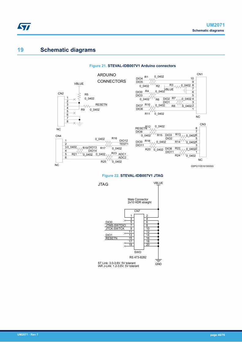
19 Schematic diagrams
Figure 21. STEVAL-IDB007V1 Arduino connectors
ARDUINOCONNECTORS
DIO0
DIO12
DIO1DIO7
DIO5
DIO0
RESETN
DIO2DIO3
DIO8
DIO4
RESETNDIO6
DIO3DIO2
DIO11DIO8DIO11
ADC1ADC2
DIO13DIO14
TEST1
VBLUE
VBLUE
R25 0_0402
R1 0_0402
R20_0402
CN1
NC
123456789
10
R60_0402
R8 0_0402
R7 0_0402
R22 0_0402
R18 0_0402
R11 0_0402R9 0_0402
R24 0_0402
R4 0_0402
R20 0_0402
R3 0_0402
R13 0_0402
R12 0_0402
CN4
NC
123456
R14 0_0402
R150_0402
R190_0402 R17 0_0402
CN3
NC
12345678
R10 0_0402
CN2
NC
12345678
R160_0402
R50_0402
R21 0_0402 R230_0402
GSPG1105161500SG
Figure 22. STEVAL-IDB007V1 JTAG
ST Link: 3.0-3.6V, 5V tolerantIAR J-Link: 1.2-3.6V, 5V tolerant
Male Connector2x10 HDR straight
RS 473-8282
JTAG
JTMS-SWTDIOJTCK-SWTCK
DIO0
DIO1RESETN
GND
VBLUE
CN7
SWD
1 23 45 67 89 10
11 1213 1415 1617 1819 20
UM2071Schematic diagrams
UM2071 - Rev 7 page 46/76
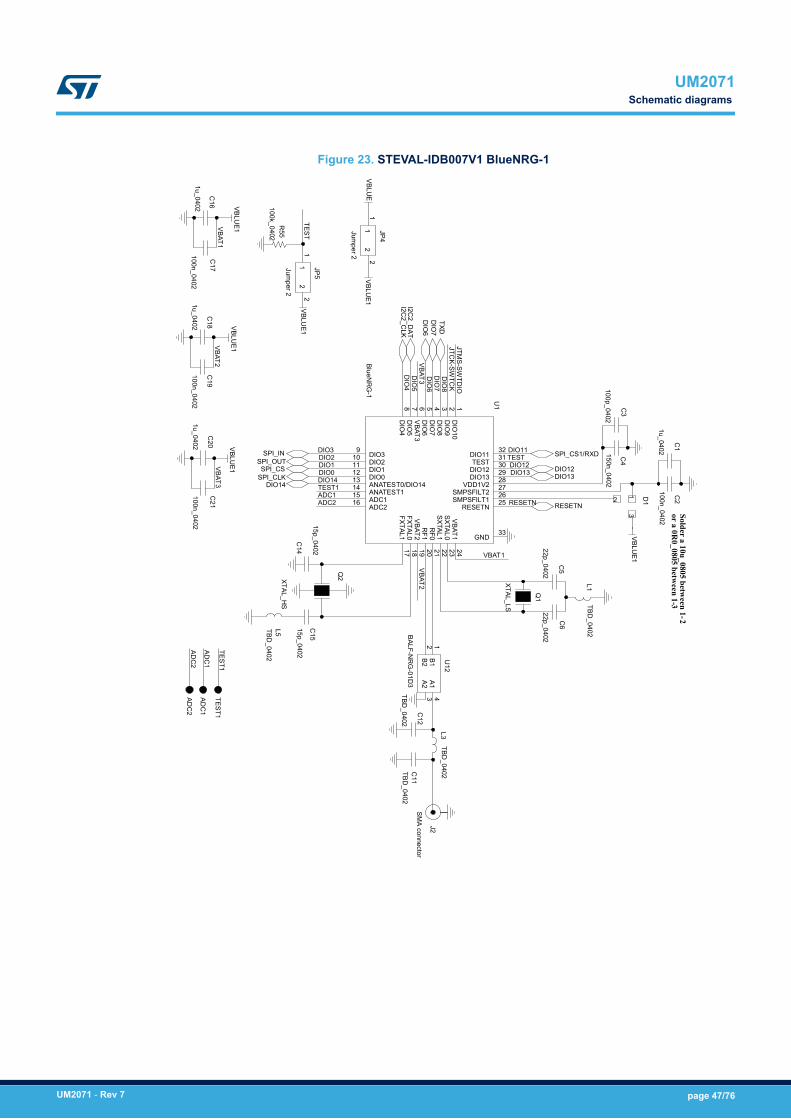
Figure 23. STEVAL-IDB007V1 BlueNRG-1
Solder a 10u_0805 between 1-2
or a 0R0_0805 betw
een 1-3
DIO3
DIO1DIO0
DIO
5
VBAT1
VBAT2
VBAT1TEST1
DIO2
VBAT2AD
C1
VBAT3
DIO
4
VBAT3 DIO
6
JTMS-SW
TDIO
JTCK-SW
TCK
RESETN
DIO13DIO12
DIO
7
TEST
ADC
2
DIO14TEST1ADC1ADC2
DIO
8
DIO11
TEST
DIO
7D
IO6
RESETN
DIO13DIO12
SPI_INSPI_OUTSPI_CS
SPI_CLK
SPI_CS1/RXD
DIO14
TXD
I2C2_D
ATI2C
2_CLK
VBLUE1
VBLUE1
VBLUE1
VBLUE1
VBLUE1
VBLUE
VBLUE1
TEST1
C2
100n_0402
C16
1u_0402
U1
BlueNR
G-1
DIO
101
DIO
92
DIO
83
DIO
74
DIO
65
VBAT36
DIO
57
DIO
48
DIO39
DIO210
DIO111
DIO012
ANATEST0/DIO1413
ANATEST114
ADC115
ADC216
DIO1132
TEST31
DIO1230
DIO1329
VDD1V228
SMPSFILT227
SMPSFILT126
RESETN25
VBAT124
SXTAL023
SXTAL122
RF0
21
RF1
20
VBAT219
FXTAL018
FXTAL117
GND33
C4
150n_0402
U12
BALF-NR
G-01D
3
B11
B22
A23
A14
C20
1u_0402
C12
TBD_0402
ADC
2
C17
100n_0402
C21
100n_0402
L5TBD_0402
Q2XTAL_H
S
JP5
Jumper 2
11
22
J2
SMA
connector
R55
100k_0402
L1TBD
_0402
C18
1u_0402
C15
15p_0402
C5
22p_0402Q
1
XTAL_LS
L3TBD
_0402
C1
1u_0402
C14
15p_0402
ADC
1
JP4
Jumper 2
11
22
C3
100p_0402
C19
100n_0402
C6
22p_0402
C11
TBD_0402
D1
1
2
3
UM2071Schematic diagrams
UM2071 - Rev 7 page 47/76
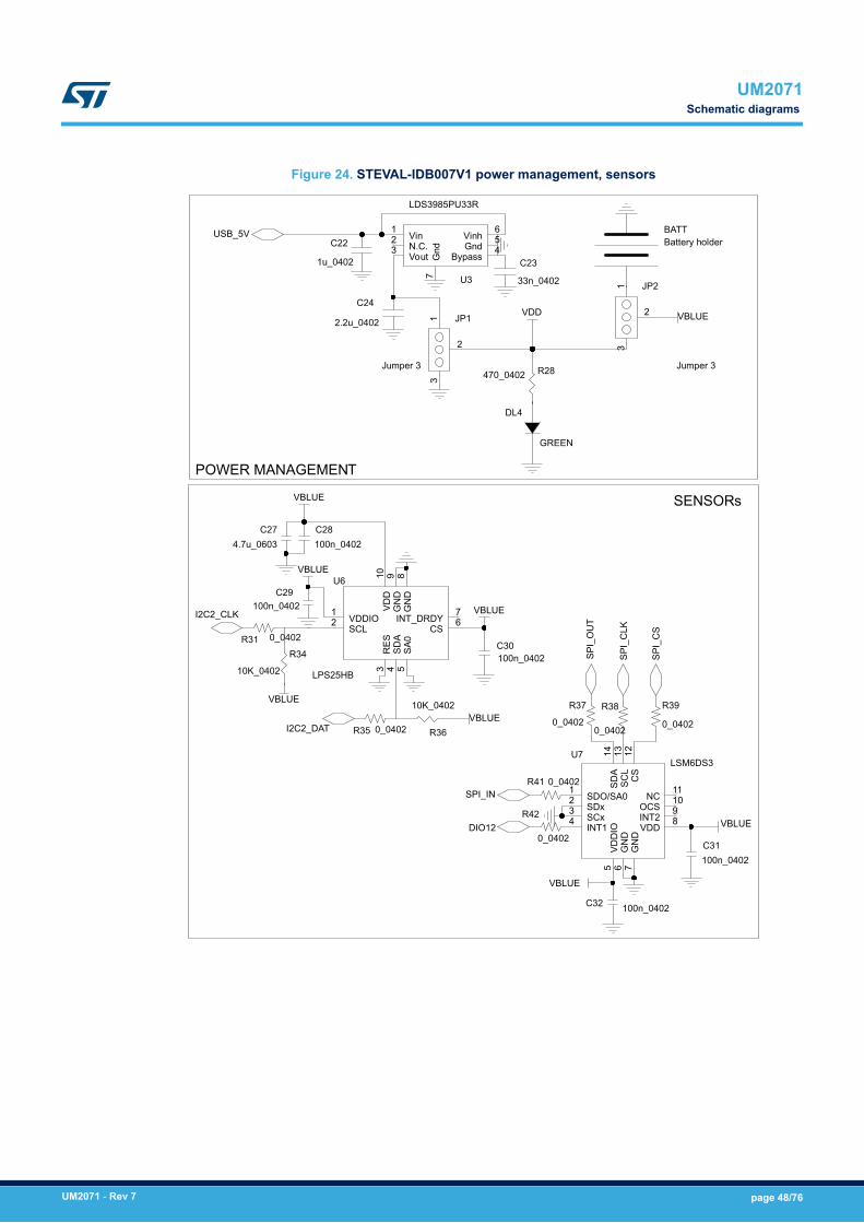
Figure 24. STEVAL-IDB007V1 power management, sensors
GREEN
POWER MANAGEMENT
SENSORs
USB_5V
SPI_
OU
T
SPI_IN
SPI_
CS
SPI_
CLK
DIO12
I2C2_DAT
I2C2_CLK
VDD VBLUE
VBLUE
VBLUE
VBLUE
VBLUE
VBLUE
VBLUE
VBLUE
C23
33n_0402
JP1
Jumper 3
1
2
3
R34
10K_0402
R37
0_0402
C22
1u_0402
R42
0_0402
R35 0_0402
R31 0_0402
U7LSM6DS3
SDO/SA01
SDx2
SCx3
INT14
VDD
IO5
GN
D6
GN
D7
SDA
14
SCL
13
CS
12
NC11
OCS10
INT29
VDD8
R28470_0402
C32 100n_0402
JP2
Jumper 3
1
2
3
U3
LDS3985PU33R
Vin1
N.C.2
Vout3
Vinh6
Gnd5
Bypass4
Gnd
7
C274.7u_0603
C30100n_0402
DL4
R38
0_0402R36
10K_0402
C28100n_0402
R41 0_0402
BATTBattery holder
C29100n_0402
R39
0_0402
C31100n_0402
U6
LPS25HB
VDDIO1
SCL2
RES
3
SDA
4
SA0
5
CS6INT_DRDY7G
ND
8G
ND
9VD
D10
C24
2.2u_0402
UM2071Schematic diagrams
UM2071 - Rev 7 page 48/76
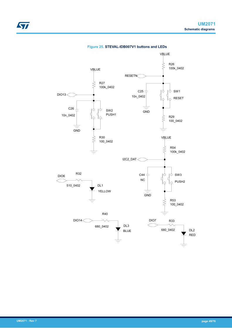
Figure 25. STEVAL-IDB007V1 buttons and LEDs
RESETN
DIO13
DIO6
DIO7DIO14
I2C2_DAT
GND
GND
VBLUE
VBLUE
GND
VBLUE
C2510n_0402
C44NC
R33
680_0402
C26
10n_0402
R32
510_0402
R26100k_0402
R54100k_0402
DL3BLUE
SW3
PUSH2
R27100k_0402
SW2PUSH1
R40
680_0402
DL1
YELLOW
R29100_0402
R30100_0402
R53100_0402
SW1
RESET
DL2RED
UM2071Schematic diagrams
UM2071 - Rev 7 page 49/76
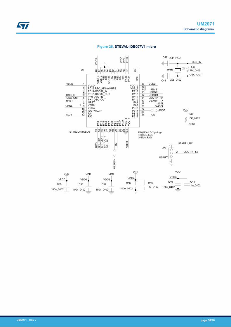
Figure 26. STEVAL-IDB007V1 micro
UFQFPN48 7x7 package128 kbyte flash16 kbyte RAM
VLCD
OSC_INOSC_OUTNRST
VDDA
USBDMUSBDP
VDD
3
VDD
1
VDD2
VLCD VDD1 VDD2 VDDA
NRST
VDD3
JTMS
JTC
KJT
DI
JTD
O
TXD1
RXD
OE
USART1_RXUSART1_TX
USART1_TX
USART1_RX
OSC_IN
OSC_OUT
PB2
SPI_
CS1
SPI_
CLK
1SP
I_O
UT1
SPI_
IN1
1-2SEL3-4SEL
DIO7R
ESET
N
VDD VDD VDDVDD
VDD
VDD
C40
100n_0402C37
100n_0402
C391u_0402
C38
100n_0402
JP3
USART
1
2
3
C42 20p_0402
U8
STM32L151CBU6
VLCD1
PC13 RTC_AF1-WKUP22
PC14-OSC32_IN3
PC15-OSC32_OUT4
PH0-OSC_IN5
PH1-OSC_OUT6
NRST7
VSSA8
VDDA9
PA0-WKUP110
PA111
PA212
PA3
13
PA4
14
PA5
15
PA6
16
PA7
17
PB0
18
PB1
19
PB2
20
PB10
21
PB11
22
VSS_
123
VDD
_124
VDD
_348
VSS_
347
PB9
46
PB8
45
BOO
T044
PB7
43
PB6
42
PB5
41
PB4
40
PB3
39
PA15
38
PA14
37
VDD_236
VSS_235
PA1334
PA1233
PA1132
PA1031
PA930
PA829
PB1528
PB1427
PB1326
PB1225
GN
D49
C35
100n_0402
C411u_0402
R4710K_0402
C43 20p_0402
X18MHz
C36
100n_0402
R511M_0402
UM2071Schematic diagrams
UM2071 - Rev 7 page 50/76
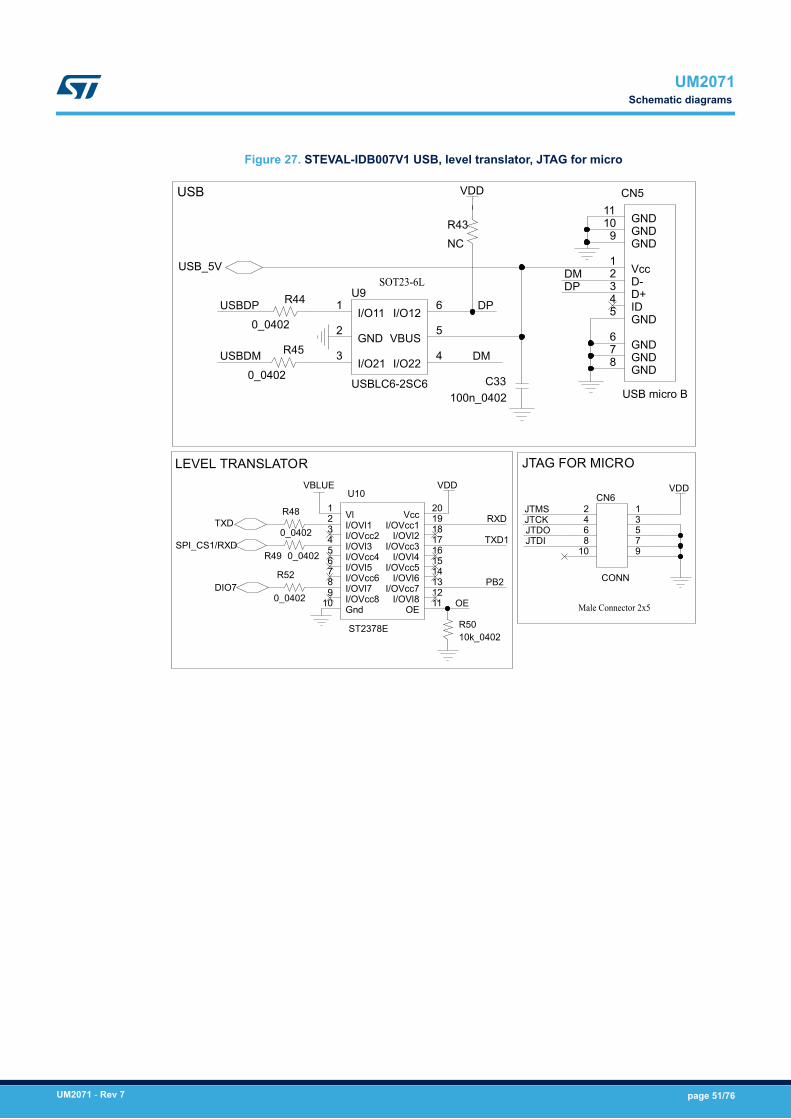
Figure 27. STEVAL-IDB007V1 USB, level translator, JTAG for micro
Male Connector 2x5
SOT23-6L
USB
JTAG FOR MICRO
JTMSJTCKJTDOJTDI
DMDP
USBDP
USBDM
DP
DM
USB_5V
VDD
VDD
R44
0_0402
CN5
USB micro B
Vcc1
D-2
D+3
ID4
GND5
GND6
GND7
GND8
GND11
GND10
GND9
C33100n_0402
U9
USBLC6-2SC6
I/O111
GND2
I/O213
I/O224
VBUS5
I/O126
CN6
CONN
12345678910
R45
0_0402
R43NC
LEVEL TRANSLATOR
OE
RXD
TXD1
PB2
TXD
SPI_CS1/RXD
DIO7
VDDVBLUEU10
ST2378E
Vl1
I/OVl12
I/OVcc23
I/OVl34
I/OVcc45
I/OVl56
I/OVcc67
I/OVl78
I/OVcc89
Gnd10
Vcc20
I/OVcc119
I/OVl218
I/OVcc317
I/OVl416
I/OVcc515
I/OVl614
I/OVcc713
I/OVl812
OE11
R49 0_0402
R52
0_0402
R5010k_0402
R48
0_0402
UM2071Schematic diagrams
UM2071 - Rev 7 page 51/76
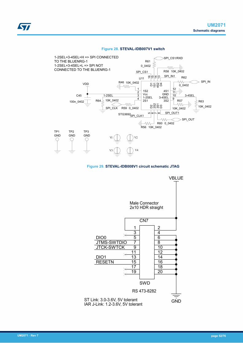
Figure 28. STEVAL-IDB007V1 switch
V1 V2
V3 V4
1-2SEL
SPI_CS1
SPI_CLK1SPI_OUT1
SPI_IN1
3-4SEL
SPI_IN
SPI_OUT
SPI_CLK
SPI_CS1/RXD
VDD
TP2GND
R610_0402
TP3GND
R58 10K_0402
R62
0_0402
R64 10K_0402 R63
10K_0402
U11
STG3692
1S21
Vcc2
1-2SEL3
2S14
D2
5
2S2
6
3S1
7
D3
8
D1
16
1S1
15
4S2
14
D4
13
4S112
GND11
3-4SEL10
3S29
R59 0_0402
C45
100n_0402
R56 10K_0402TP1GND
R60 0_0402
R46 10K_0402
R57
10K_0402
1-2SEL=3-4SEL=H => SPI CONNECTEDTO THE BLUENRG-11-2SEL=3-4SEL=L => SPI NOTCONNECTED TO THE BLUENRG-1
Figure 29. STEVAL-IDB008V1 circuit schematic JTAG
ST Link: 3.0-3.6V, 5V tolerantIAR J-Link: 1.2-3.6V, 5V tolerant
Male Connector2x10 HDR straight
RS 473-8282
JTMS-SWTDIOJTCK-SWTCK
DIO0
DIO1RESETN
GND
VBLUE
CN7
SWD
1 23 45 67 89 10
11 1213 1415 1617 1819 20
UM2071Schematic diagrams
UM2071 - Rev 7 page 52/76
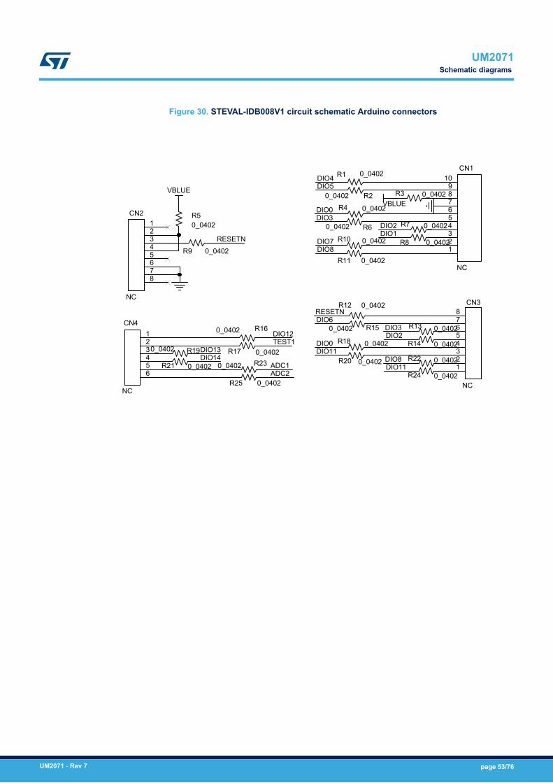
Figure 30. STEVAL-IDB008V1 circuit schematic Arduino connectors
DIO0
DIO12
DIO1DIO7
DIO5
DIO0
RESETN
DIO2DIO3
DIO8
DIO4
RESETNDIO6
DIO3DIO2
DIO11DIO8DIO11ADC1
ADC2
DIO13DIO14
TEST1
VBLUE
VBLUE
R24 0_0402
R22 0_0402
R160_0402
R1 0_0402
R25 0_0402
R7 0_0402
CN4
NC
123456
R230_0402
R4 0_0402
R21 0_0402
R18 0_0402
R20 0_0402
R150_0402
R190_0402 R17 0_0402
CN1
NC
123456789
10
R12 0_0402
R20_0402
CN3
NC
12345678
R14 0_0402
R13 0_0402
R11 0_0402
R8 0_0402R9 0_0402
R10 0_0402
CN2
NC
12345678
R60_0402
R3 0_0402
R50_0402
UM2071Schematic diagrams
UM2071 - Rev 7 page 53/76
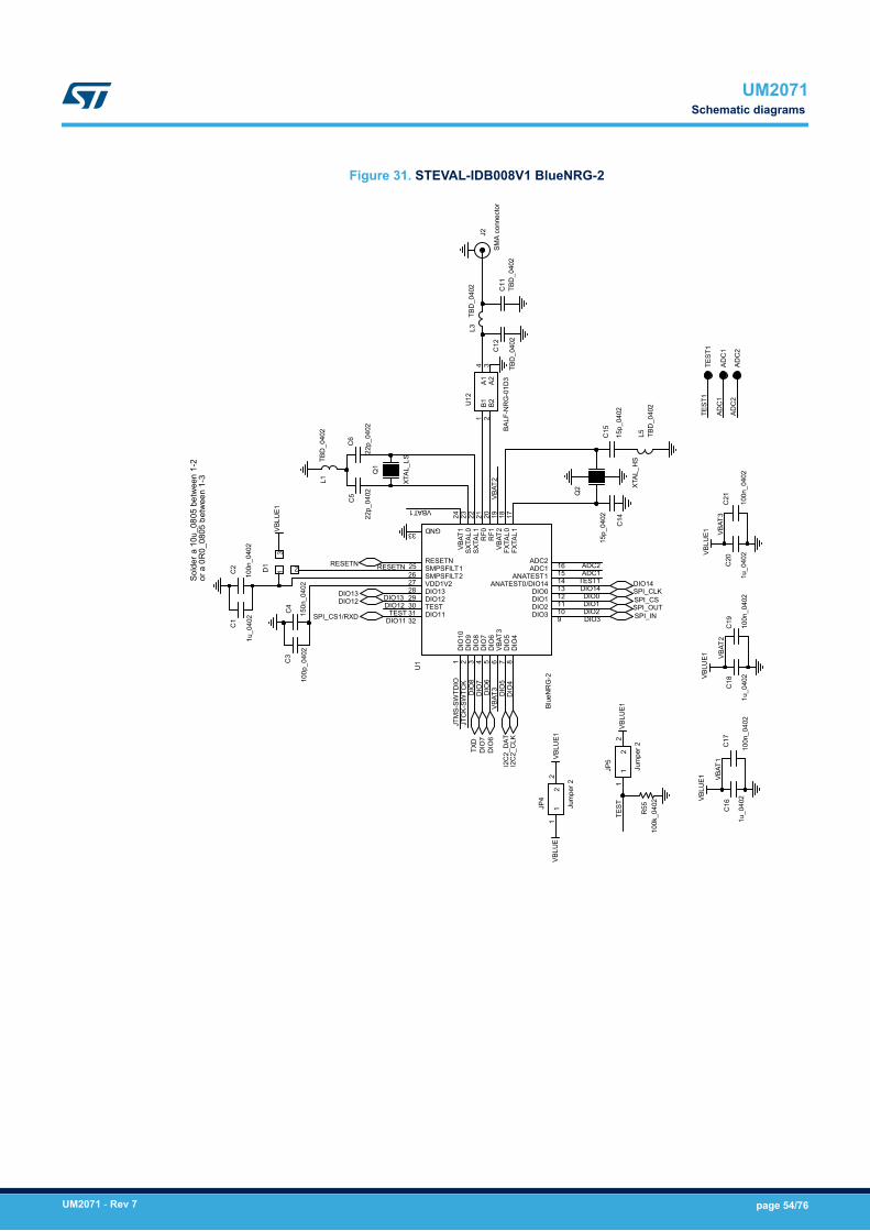
Figure 31. STEVAL-IDB008V1 BlueNRG-2So
lder
a 1
0u_0
805
betw
een
1-2
or a
0R
0_08
05 b
etw
een
1-3
DIO3
DIO1DIO0
DIO
5
VBAT1
VBAT
2
VBAT
1
TEST
1
DIO2
VBAT
2AD
C1
VBAT
3
DIO
4
VBAT
3DIO
6
JTM
S-SW
TDIO
JTC
K-SW
TCK
RESETN
DIO13DIO12
DIO
7
TEST
ADC
2
DIO14TEST1ADC1ADC2
DIO
8
DIO11TE
ST
DIO
7D
IO6
RESETN
DIO13DIO12
SPI_INSPI_OUTSPI_CSSPI_CLK
SPI_CS1/RXD
DIO14
TXD
I2C
2_D
ATI2
C2_
CLK
VBLU
E1
VBLU
E1VB
LUE1
VBLU
E1
VBLU
E1
VBLU
EVB
LUE1
U12
BALF
-NR
G-0
1D3
B11
B22
A23
A14
Q1
XTAL
_LS
C12
TBD
_040
2
L3TB
D_0
402
L1TB
D_0
402
C3
100p
_040
2
C2
100n
_040
2
C17
100n
_040
2
C21
100n
_040
2
C20
1u_0
402
R55
100k
_040
2
JP4
Jum
per 2
11
22
TEST
1
Q2 XT
AL_H
S
J2
SMA
conn
ecto
r
D1
1
2
3
C19
100n
_040
2
C1
1u_0
402
C18
1u_0
402
C6
22p_
0402
C11
TBD
_040
2
C16
1u_0
402
U1
Blue
NR
G-2
DIO
101
DIO
92
DIO
83
DIO
74
DIO
65
VBAT
36
DIO
57
DIO
48
DIO39
DIO210
DIO111
DIO012
ANATEST0/DIO1413
ANATEST114
ADC115
ADC216
DIO1132
TEST31
DIO1230
DIO1329
VDD1V228
SMPSFILT227
SMPSFILT126
RESETN25
VBAT
124
SXTA
L023
SXTA
L122
RF0
21
RF1
20
VBAT
219
FXTA
L018
FXTA
L117
GND33
L5 TBD
_040
2
C5
22p_
0402
C4
150n
_040
2
ADC
2
JP5
Jum
per 2
11
22
C14
15p_
0402
ADC
1
C15
15p_
0402
UM2071Schematic diagrams
UM2071 - Rev 7 page 54/76
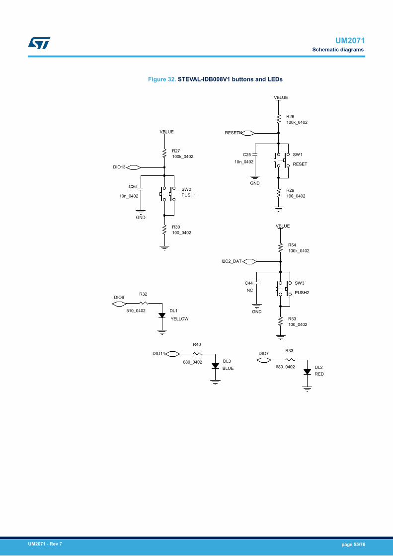
Figure 32. STEVAL-IDB008V1 buttons and LEDs
RESETN
DIO13
DIO6
DIO7DIO14
I2C2_DAT
GND
GND
VBLUE
VBLUE
GND
VBLUE
SW1
RESET
R32
510_0402
SW3
PUSH2
DL3BLUE
R33
680_0402
R54100k_0402
R27100k_0402
SW2PUSH1
DL2RED
C44NC
R26100k_0402
C26
10n_0402
R53100_0402
C2510n_0402
R40
680_0402
DL1
YELLOW
R30100_0402
R29100_0402
UM2071Schematic diagrams
UM2071 - Rev 7 page 55/76
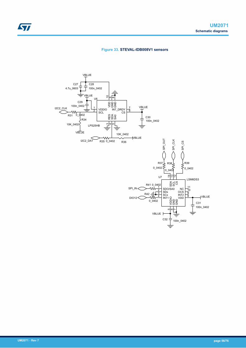
Figure 33. STEVAL-IDB008V1 sensors
SPI_
OU
T
SPI_IN
SPI_
CS
SPI_
CLK
DIO12
I2C2_DAT
I2C2_CLK
VBLUE
VBLUE
VBLUE
VBLUE
VBLUE
VBLUE
VBLUE
R34
10K_0402
R37
0_0402
R35 0_0402
R41 0_0402
C28100n_0402
C30100n_0402
R42
0_0402
U7LSM6DS3
SDO/SA01
SDx2
SCx3
INT14
VDD
IO5
GN
D6
GN
D7
SDA
14
SCL
13
CS
12
NC11
OCS10
INT29
VDD8
R39
0_0402
R36
10K_0402
C32 100n_0402
R31 0_0402
C274.7u_0603
R38
0_0402
C29100n_0402
C31100n_0402
U6
LPS25HB
VDDIO1
SCL2
RES
3
SDA
4
SA0
5CS
6INT_DRDY7G
ND
8G
ND
9VD
D10
UM2071Schematic diagrams
UM2071 - Rev 7 page 56/76
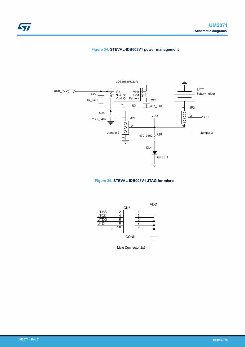
GREEN
Figure 34. STEVAL-IDB008V1 power management
USB_5V
VDD VBLUEJP1
Jumper 3
12
3
DL4
BATTBattery holder
C23
33n_0402
C24
2.2u_0402
R28470_0402
U3
LDS3985PU33R
Vin1
N.C.2
Vout3
Vinh6
Gnd5
Bypass4
Gnd
7
C22
1u_0402
JP2
Jumper 3
1
2
3Figure 35. STEVAL-IDB008V1 JTAG for micro
Male Connector 2x5
JTMSJTCKJTDOJTDI
VDDCN6
CONN
12345678910
UM2071Schematic diagrams
UM2071 - Rev 7 page 57/76
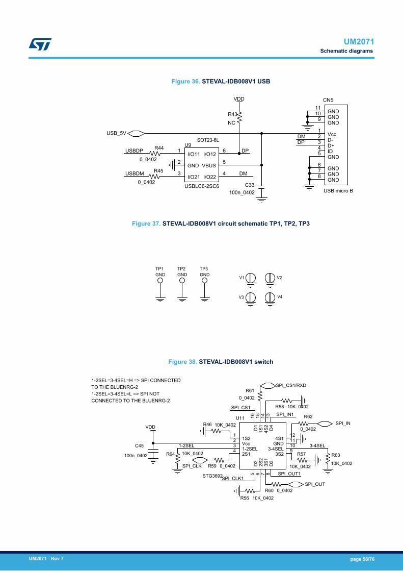
Figure 36. STEVAL-IDB008V1 USB
SOT23-6LDMDP
USBDP
USBDM
DP
DM
USB_5V
VDD
R45
0_0402
R44
0_0402
R43NC
CN5
USB micro B
Vcc1
D-2
D+3
ID4
GND5
GND6
GND7
GND8
GND11
GND10
GND9
C33100n_0402
U9
USBLC6-2SC6
I/O111
GND2
I/O213
I/O224
VBUS5
I/O126
Figure 37. STEVAL-IDB008V1 circuit schematic TP1, TP2, TP3
V1 V2
V3 V4
TP1GND
TP3GND
TP2GND
Figure 38. STEVAL-IDB008V1 switch
1-2SEL=3-4SEL=H => SPI CONNECTEDTO THE BLUENRG-21-2SEL=3-4SEL=L => SPI NOTCONNECTED TO THE BLUENRG-2
1-2SEL
SPI_CS1
SPI_CLK1SPI_OUT1
SPI_IN1
3-4SEL
SPI_IN
SPI_OUT
SPI_CLK
SPI_CS1/RXD
VDD
R59 0_0402
R63
10K_0402
R610_0402
R58 10K_0402
R56 10K_0402
U11
STG3692
1S21
Vcc2
1-2SEL3
2S14
D2
5
2S2
6
3S1
7
D3
8
D1
16
1S1
15
4S2
14
D4
13
4S112
GND11
3-4SEL10
3S29
C45
100n_0402
R60 0_0402
R64 10K_0402 R57
10K_0402
R62
0_0402R46 10K_0402
UM2071Schematic diagrams
UM2071 - Rev 7 page 58/76
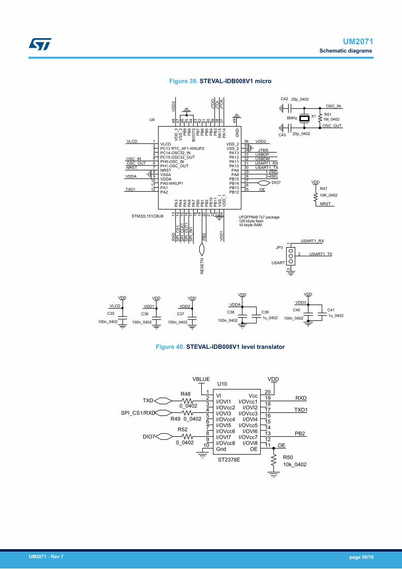
Figure 39. STEVAL-IDB008V1 micro
UFQFPN48 7x7 package128 kbyte flash16 kbyte RAM
VLCD
OSC_INOSC_OUTNRST
VDDA
USBDMUSBDP
VDD
3
VDD
1
VDD2
VLCD VDD1 VDD2 VDDA
NRST
VDD3
JTMS
JTC
KJT
DI
JTD
O
TXD1
RXD
OE
USART1_RXUSART1_TX
USART1_TX
USART1_RX
OSC_IN
OSC_OUT
PB2
SPI_
CS1
SPI_
CLK
1SP
I_O
UT1
SPI_
IN1
1-2SEL3-4SEL
DIO7
RES
ETN
VDD VDD VDDVDD
VDD
VDD
C35
100n_0402
C42 20p_0402
X18MHzU8
STM32L151CBU6
VLCD1
PC13 RTC_AF1-WKUP22
PC14-OSC32_IN3
PC15-OSC32_OUT4
PH0-OSC_IN5
PH1-OSC_OUT6
NRST7
VSSA8
VDDA9
PA0-WKUP110
PA111
PA212
PA3
13
PA4
14
PA5
15
PA6
16
PA7
17
PB0
18
PB1
19
PB2
20
PB10
21
PB11
22
VSS_
123
VDD
_124
VDD
_348
VSS_
347
PB9
46
PB8
45
BOO
T044
PB7
43
PB6
42
PB5
41
PB4
40
PB3
39
PA15
38
PA14
37
VDD_236
VSS_235
PA1334
PA1233
PA1132
PA1031
PA930
PA829
PB1528
PB1427
PB1326
PB1225
GN
D49
R511M_0402
C40
100n_0402C37
100n_0402
C38
100n_0402
C391u_0402
C36
100n_0402
C411u_0402
C43 20p_0402
R4710K_0402
JP3
USART
1
2
3
Figure 40. STEVAL-IDB008V1 level translator
OE
RXD
TXD1
PB2
TXD
SPI_CS1/RXD
DIO7
VDDVBLUE
R48
0_0402
U10
ST2378E
Vl1
I/OVl12
I/OVcc23
I/OVl34
I/OVcc45
I/OVl56
I/OVcc67
I/OVl78
I/OVcc89
Gnd10
Vcc20
I/OVcc119
I/OVl218
I/OVcc317
I/OVl416
I/OVcc515
I/OVl614
I/OVcc713
I/OVl812
OE11
R5010k_0402
R52
0_0402
R49 0_0402
UM2071Schematic diagrams
UM2071 - Rev 7 page 59/76
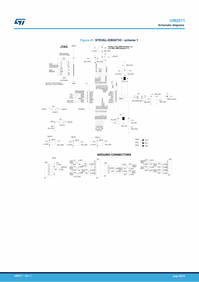
Figure 41. STEVAL-IDB007V2 - scheme 1
VBLUE
6
1112
DIO
12
DIO0
R2
150n_0402
VBLUE
SMPS
FILT
1
0_0402
5
R3
R20 0_0402
19
0_0402
R1 87654321
JTCK-SWTCK
DIO8
L5
R110_0402
DIO5
NC
0_0402
DIO4
VBAT1
NC
C12
DIO7
ADC1
DIO13
DIO3
8
B2
BALF-NRG-02D3
2
VBLUE1
TBD_0402
C18
32D
IO11
TEST
DIO75DIO6
24
RESETN
25R
ESET
N
ADC2
CN7
VBLUE1
C20
4
DIO
3
SWD
DIO
111
22SXTAL1
RF021
100k_0402
L1
15p_0402
R190_0402
TEST1
0_0402
ADC2
I2C2_DAT
A23
TEST1
SPI_
IN
DIO6
Jumper 2
22
18
DIO2
11
DIO0
DIO14
RS 473-8282
ST Link: 3.0-3.6V, 5V tolerantIAR J-Link: 1.2-3.6V, 5V tolerant
33
DIO
0
C2
DIO7
VBAT37DIO5
VBAT
1
13
DIO
11
XTAL_LS
23SXTAL0
R25
J2
0_0402
R21
C4
Q1
VBLUE
TXDA1
4SP
I_O
UT
DIO
13
100n_0402
C16
JP4
VBLUE1
DIO8
FXTAL1
DIO8
GN
D
JTMS-SWTDIO
DIO1
17
ADC
2
0_0402
R55
11
TEST1
JTAG
12345678
R16
Male Connector2x10 HDR straight
0_0402
C1
2 0_0402RESETRN
1
CN4
NC
RF1 VBAT2
22p_0402
R5
31 30D
IO12
7
XTAL_HS
R9
DIO
13
DIO4987654321
14
DIO
3D
IO2
10
10
DIO11
29D
IO13
U12
DIO0
1516
GND
0_0402
R24
2
0_0402 R17
TBD_0402
169
DIO4
ADC1
CN3
NC
0_0402
3
0_0402
DIO5
D1
2
1u_0402
U1
R6
C3
6
DIO
12
100n_0402
DIO7
VBLUE
1918
Jumper 2
22
R10 0_0402
C19
C6
1
ADC
2
VBAT2
8
VBAT3
DIO102
4
C17
VBLUE1
I2C2_CLK
3
1u_0402
DIO
0
0_0402
CN1
RESETN
BlueNRG-1
1
DIO6
0_0402
123456
C15
9
DIO
14SP
I_C
LK
100p_0402
VBAT1
DIO2
RES
ETN
DIO12
0_0402
B11
0_0402 R13
100n_0402
C21
0_0402
JP5
10
14AN
ATES
T1AD
C1
15
VBLUE1
ADC
1
JTMS-SWTDIO
R18
DIO1
VBAT3
ANAT
EST0
/DIO
14
DIO6
1u_0402
FXTAL0 17
0_0402ADC1
DIO
2
RES
ETN
C14
22p_0402
R14
28VD
D1V
2
1
TEST
0_0402 R22DIO3
SPI_
CS
Solder a 10u_0805 between 1-2or a 0R0_0805 between 1-3
JTCK-SWTCK
0_0402 0_0402
C11
27SM
PSFI
LT2
26
20
20
VBAT2D
IO1
TEST
1
DIO93DIO8
100n_0402
CN2
12 13
TEST
L3 TBD_0402
R15
DIO11
TBD_0402
Q2
R23
15p_0402
C5
TBD_0402
R7
ARDUINO CONNECTORS
ADC2
SPI_
CS1
/RXD
DIO
14
1u_0402
R8
VBLUE1
R4
SMA connector
UM2071Schematic diagrams
UM2071 - Rev 7 page 60/76
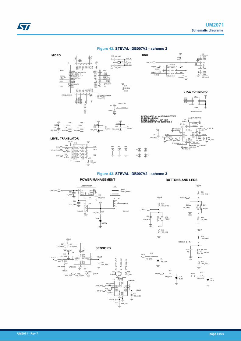
Figure 42. STEVAL-IDB007V2 - scheme 2
14
D4
13
GND7
33
PA1132
NRST
SPI_
CS1
1
VDD
19
PB2
20
PB8
14I/OVl6
VBLUE
Vcc20
USB micro B
D-2
100n_0402
R62
PB2
10K_0402
R47
4
100n_0402
JP3
6
5
GND
5
46
DIO7
SPI_CS1/RXD
24VD
D_1
38
PA14
37
3
0_0402
PB10
21
VDD2
0_0402
U10
VDD3
R52
SPI_IN1C35
R490_0402
TP3
I/OVcc5
6GND
RXD
45PA
6
SPI_
CLK
1
C37
D+3
VLCDPC13 RTC_AF1-WKUP2PC14-OSC32_INPC15-OSC32_OUTPH0-OSC_INPH1-OSC_OUTNRSTVSSAVDDAPA0-WKUP1PA1PA2
GND11
USART
2
SOT23-6L
I/O22
5VBUS
CN6
MICRO
12
1S1
VDD
1 6
23VS
S_1
PA5
15
SPI_CLK
PA12
TP1
30
PA829
100n_0402
R44
OE
PB4
40
VDD
3
7
18I/OVl2 17
C361u_0402
R61
SPI_OUTSPI_CLK1
I/OVcc46
1-2SEL
GN
D49
2Vcc
C42 20p_0402
C33
U9
100n_0402
USB
4S112
Male Connector 2x5
Vl
ST2378E
1
7
48VD
D_3
VSS_
3
VDDA
50_0402
R43
JTDO
17
SPI_CS1/RXD
I/OVcc24
13I/OVcc68
USART1_TX
C41
DM
11
I/O12
U8 Vcc1
16
PA7
SPI_INC40
USBDM
DP
1
VDDA
4
8JTDI
100n_0402
10k_0402
BOO
T044
25
3
PB5
41
USART1_TX
DIO7 I/OVl79
PB1528
VDD1
VDD
X1
1
VDD
PB11
22
19TXD
6
PB3
100n_0402
R48
PB0
18
9
GND11
USBDP
JTAG FOR MICRO
I/OVl4
STG3692
11S2
USART1_RX
1M_0402
PA1334
D1
16
26
PB12
VDD
CONN
1
43
JTCK
16
JTD
I
PA3
GND8I/O21
4
USART1_RX
I/OVl8OE
I/OVcc8Gnd
10
C39
R63
10
GND9
USBDP
USB_5V
1u_0402
20p_0402
U11
9
NC
TXD1
PB2
OSC_IN
13
PA4
14
15
VDD
I/OVl13
62S
2
USBDM
PB13
JTMS
JTMS
VDD
RES
ETN
D3
8
1-2SEL
3VDD_2
36
12
47
PB9
TXD1
SPI_
OU
T18
VDD
SPI_CS1
PB1427
PA10
10K_0402
5GND
3-4SEL109
10
OE
VDD
R590_0402
PB7
11
RXD
R45
R600_0402R5610K_0402
10K_0402
USBLC6-2SC6
I/O11
GND2
8MHz
PB6
42
R5810K_0402
C38
JTD
O
SPI_OUT1
3
JTC
K
OSC_OUT
0_0402
CN5
R46 10K_0402
R57
VDD
3
3-4SEL
2
1-2SEL=3-4SEL=H => SPI CONNECTEDTO THE BLUENRG-11-2SEL=3-4SEL=L => SPI NOTCONNECTED TO THE BLUENRG-1
VLCD
C45
VLCD
VSS_235
100n_0402
TP2
DMDP
ID4
15
4S2
SPI_
IN1 2
I/OVcc3
3-4SEL3S2
31
PA9
I/OVl35
GND
PB1
10
C430_0402
R51
LEVEL TRANSLATOR
73S
1
UFQFPN48 7x7 package128 kbyte flash16 kbyte RAM
V1V2
V3 V4
R50
R64 10K_0402
D2
1-2SEL2S1
OSC_OUT
I/OVcc1
4
I/OVl57
0_0402
OSC_IN
I/OVcc7
NRST
39
PA15
VDD
GND GND
VDD2
STM32L151CBU6
2
55
Figure 43. STEVAL-IDB007V2 - scheme 3
100_0402
R36
SW1
R35 0_0402 0_0402
9
SPI_
OU
T
DIO7
VDD
IOG
ND
6
U6
100n_0402
0_04020_0402R33
VBLUE
100_0402
R53CS
6
13
CS
12
R27
100n_0402
SPI_IN
4
DIO6
VBLUE
SW3
10
VBLUE
VBLUE
100k_0402
R54
SW2
100n_0402
LPS25HB
1
PUSH1
INT1
SPI_
CS
5
10n_0402
DIO13
BLUE
NC
BUTTONS AND LEDS
SA0
5
4.7u_0603
C30
VBLUE
10n_0402
C44NC
680_0402
100k_0402
DL3
SPI_
CLK
RED
100_0402
RESETN
SCL
SENSORS
POWER MANAGEMENT
VBLUE
RESET
GND
0_0402
R410_0402
R30
11
R34
DIO12
C31
VBLUE
R26
7
10K_0402
R37
C27I2C2_DAT
I2C2_DAT
DL2
PUSH2
GN
D7
4SD
A YELLOW
R29
LSM6DS3
1
R40
C32
GN
D8
INT_DRDY
SDO/SA02SDx
R32
10K_0402
C28
VDDIO2SCL
C29
I2C2_CLK
SDA
14
DL1
VDD
INT2VDD
8
100n_0402
OCS
U7
R31 0_0402
VBLUE
3R
ES
R42
680_0402
100k_0402
R38
GND
100n_0402
R39DIO14
510_0402
9G
ND
GND
VBLUE
C26
C25
Gnd5
3
3
VBLUE
1Vin
33n_0402
JP1
U3
C22
DL4
C24
Vout
6Vinh
JP2
LDS3985PU33R
2N.C.
VDD
1
C23
2.2u_0402
BATT
3
1
Battery holder
2
Jumper 3470_0402 R28
Gnd
7
Bypass4
1u_0402
GREEN
USB_5V
2
Jumper 3
103
SCx
VBLUE
UM2071Schematic diagrams
UM2071 - Rev 7 page 61/76
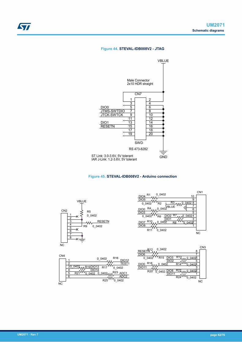
Figure 44. STEVAL-IDB008V2 - JTAG
ST Link: 3.0-3.6V, 5V tolerantIAR J-Link: 1.2-3.6V, 5V tolerant
Male Connector2x10 HDR straight
RS 473-8282
JTMS-SWTDIOJTCK-SWTCK
DIO0
DIO1RESETN
GND
VBLUE
CN7
SWD
1 23 45 67 89 10
11 1213 1415 1617 1819 20
Figure 45. STEVAL-IDB008V2 - Arduino connection
DIO0
DIO12
DIO1DIO7
DIO5
DIO0
RESETN
DIO2DIO3
DIO8
DIO4
RESETNDIO6
DIO3DIO2
DIO11DIO8DIO11ADC1
ADC2
DIO13DIO14
TEST1
VBLUE
VBLUE
R24 0_0402
R22 0_0402
R160_0402
R1 0_0402
R25 0_0402
R7 0_0402
CN4
NC
123456
R230_0402
R4 0_0402
R21 0_0402
R18 0_0402
R20 0_0402
R150_0402
R190_0402 R17 0_0402
CN1
NC
123456789
10
R12 0_0402
R20_0402
CN3
NC
12345678
R14 0_0402
R13 0_0402
R11 0_0402
R8 0_0402R9 0_0402
R10 0_0402
CN2
NC
12345678
R60_0402
R3 0_0402
R50_0402
UM2071Schematic diagrams
UM2071 - Rev 7 page 62/76
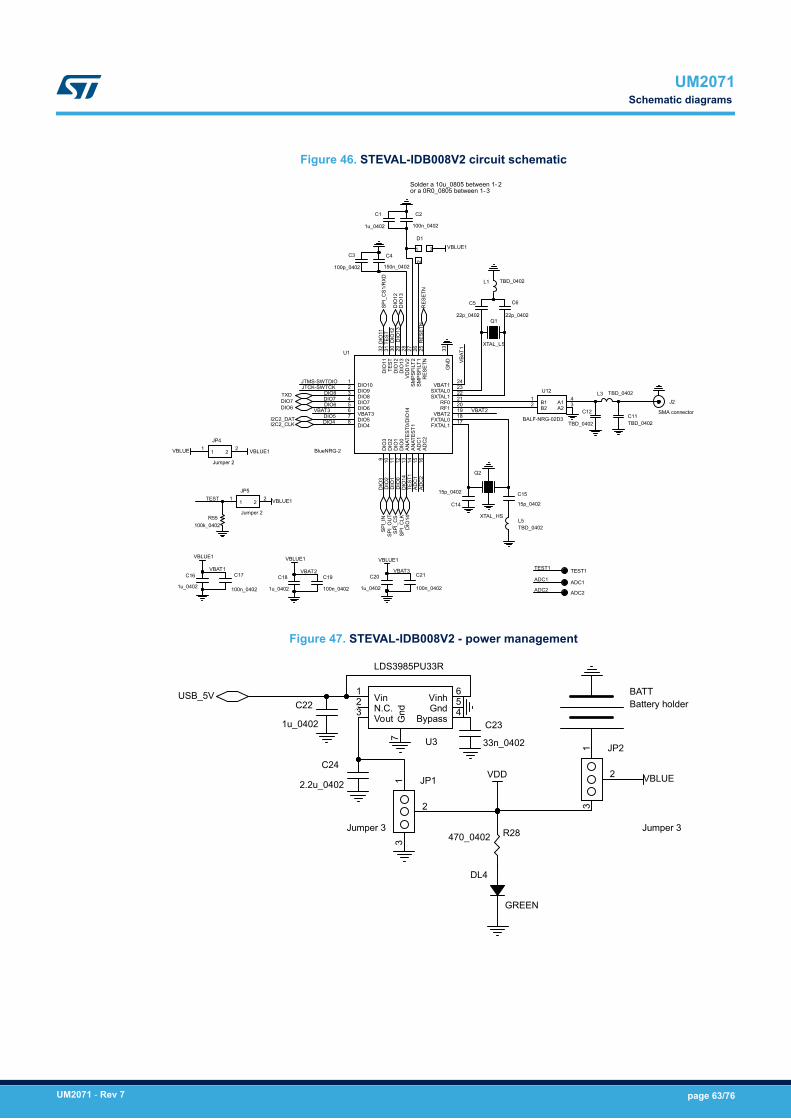
Figure 46. STEVAL-IDB008V2 circuit schematic
Solder a 10u_0805 between 1- 2or a 0R0_0805 between 1- 3
DIO
3
DIO
1D
IO0
DIO5
VBAT
1
VBAT2
VBAT1 TEST1
DIO
2
VBAT2ADC1
VBAT3
DIO4
VBAT3DIO6
JTMS-SWTDIOJTCK-SWTCK
RES
ETN
DIO
13D
IO12
DIO7
TEST
ADC2
DIO
14TE
ST1
ADC
1AD
C2
DIO8
DIO
11
TEST
DIO7DIO6
RES
ETN
DIO
13D
IO12
SPI_
INSP
I_O
UT
SPI_
CS
SPI_
CLK
SPI_
CS1
/RXD
DIO
14
TXD
I2C2_DATI2C2_CLK
VBLUE1
VBLUE1 VBLUE1VBLUE1
VBLUE1
VBLUE VBLUE1
U12
BALF-NRG-02D3
B11
B22
A23A14
Q1
XTAL_LS
C12
TBD_0402
L3 TBD_0402
L1 TBD_0402
C3
100p_0402
C2
100n_0402
C17
100n_0402
C21
100n_0402
C20
1u_0402
R55100k_0402
JP4
Jumper 2
11
22
TEST1
Q2
XTAL_HS
J2
SMA connector
D1
1
2
3
C19
100n_0402
C1
1u_0402
C18
1u_0402
C6
22p_0402
C11TBD_0402
C16
1u_0402
U1
BlueNRG-2
DIO101
DIO92
DIO83
DIO74
DIO65
VBAT36
DIO57
DIO48
DIO
39
DIO
210
DIO
111
DIO
012
ANAT
EST0
/DIO
1413
ANAT
EST1
14
ADC
115
ADC
216
DIO
1132
TEST
31
DIO
1230
DIO
1329
VDD
1V2
28
SMPS
FILT
227
SMPS
FILT
126
RES
ETN
25
VBAT124
SXTAL023
SXTAL122
RF021
RF120
VBAT219
FXTAL018
FXTAL117
GN
D33
L5TBD_0402
C5
22p_0402
C4
150n_0402
ADC2
JP5
Jumper 2
11
22
C14
15p_0402
ADC1
C15
15p_0402
Figure 47. STEVAL-IDB008V2 - power management
GREEN
USB_5V
VDD VBLUEJP1
Jumper 3
1
2
3
DL4
BATTBattery holder
C23
33n_0402
C24
2.2u_0402
R28470_0402
U3
LDS3985PU33R
Vin1
N.C.2
Vout3
Vinh6
Gnd5
Bypass4
Gnd
7
C22
1u_0402
JP2
Jumper 3
1
2
3
UM2071Schematic diagrams
UM2071 - Rev 7 page 63/76
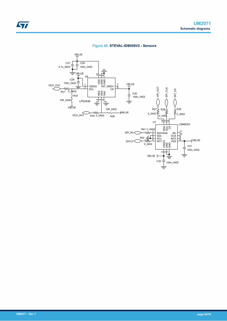
Figure 48. STEVAL-IDB008V2 - Sensors
SPI_
OU
T
SPI_IN
SPI_
CS
SPI_
CLK
DIO12
I2C2_DAT
I2C2_CLK
VBLUE
VBLUE
VBLUE
VBLUE
VBLUE
VBLUE
VBLUE
R34
10K_0402
R37
0_0402R35 0_0402
R41 0_0402
C28100n_0402
C30100n_0402
R42
0_0402
U7LSM6DS3
SDO/SA01
SDx2
SCx3
INT14
VDD
IO5
GN
D6
GN
D7
SDA
14
SCL
13
CS
12
NC11
OCS10
INT29
VDD8
R39
0_0402R36
10K_0402
C32 100n_0402
R31 0_0402
C274.7u_0603
R38
0_0402
C29100n_0402
C31100n_0402
U6
LPS25HB
VDDIO1
SCL2
RES
3
SDA
4
SA0
5
CS6INT_DRDY7G
ND
8G
ND
9VD
D10
UM2071Schematic diagrams
UM2071 - Rev 7 page 64/76

Figure 49. STEVAL-IDB008V2 - buttons and LEDs
RESETN
DIO13
DIO6
DIO7DIO14
I2C2_DAT
GND
GND
VBLUE
VBLUE
GND
VBLUE
SW1
RESET
R32
510_0402
SW3
PUSH2
DL3BLUE
R33
680_0402
R54100k_0402
R27100k_0402
SW2PUSH1
DL2RED
C44NC
R26100k_0402
C26
10n_0402
R53100_0402
C2510n_0402
R40
680_0402
DL1
YELLOW
R30100_0402
R29100_0402
UM2071Schematic diagrams
UM2071 - Rev 7 page 65/76
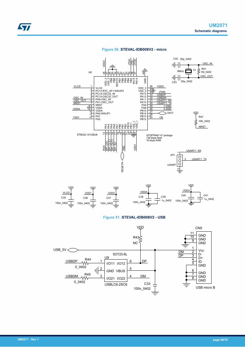
Figure 50. STEVAL-IDB008V2 - micro
UFQFPN48 7x7 package128 kbyte flash16 kbyte RAM
VLCD
OSC_INOSC_OUTNRST
VDDA
USBDMUSBDP
VDD
3
VDD
1
VDD2
VLCD VDD1 VDD2 VDDA
NRST
VDD3
JTMS
JTC
KJT
DI
JTD
O
TXD1
RXD
OE
USART1_RXUSART1_TX
USART1_TX
USART1_RX
OSC_IN
OSC_OUT
PB2
SPI_
CS1
SPI_
CLK
1SP
I_O
UT1
SPI_
IN1
1-2SEL3-4SEL
DIO7
RES
ETN
VDD VDD VDDVDD
VDD
VDD
C35
100n_0402
C42 20p_0402
X18MHzU8
STM32L151CBU6
VLCD1
PC13 RTC_AF1-WKUP22
PC14-OSC32_IN3
PC15-OSC32_OUT4
PH0-OSC_IN5
PH1-OSC_OUT6
NRST7
VSSA8
VDDA9
PA0-WKUP110
PA111
PA212
PA3
13
PA4
14
PA5
15
PA6
16
PA7
17
PB0
18
PB1
19
PB2
20
PB10
21
PB11
22
VSS_
123
VDD
_124
VDD
_348
VSS_
347
PB9
46
PB8
45
BOO
T044
PB7
43
PB6
42
PB5
41
PB4
40
PB3
39
PA15
38
PA14
37
VDD_236
VSS_235
PA1334
PA1233
PA1132
PA1031
PA930
PA829
PB1528
PB1427
PB1326
PB1225
GN
D49
R511M_0402
C40
100n_0402C37
100n_0402
C38
100n_0402
C391u_0402
C36
100n_0402
C411u_0402
C43 20p_0402
R4710K_0402
JP3
USART
1
2
3
Figure 51. STEVAL-IDB008V2 - USB
SOT23-6LDMDP
USBDP
USBDM
DP
DM
USB_5V
VDD
R45
0_0402
R44
0_0402
R43NC
CN5
USB micro B
Vcc1
D-2
D+3
ID4
GND5
GND6
GND7
GND8
GND11
GND10
GND9
C33100n_0402
U9
USBLC6-2SC6
I/O111
GND2
I/O213
I/O224
VBUS5
I/O126
UM2071Schematic diagrams
UM2071 - Rev 7 page 66/76
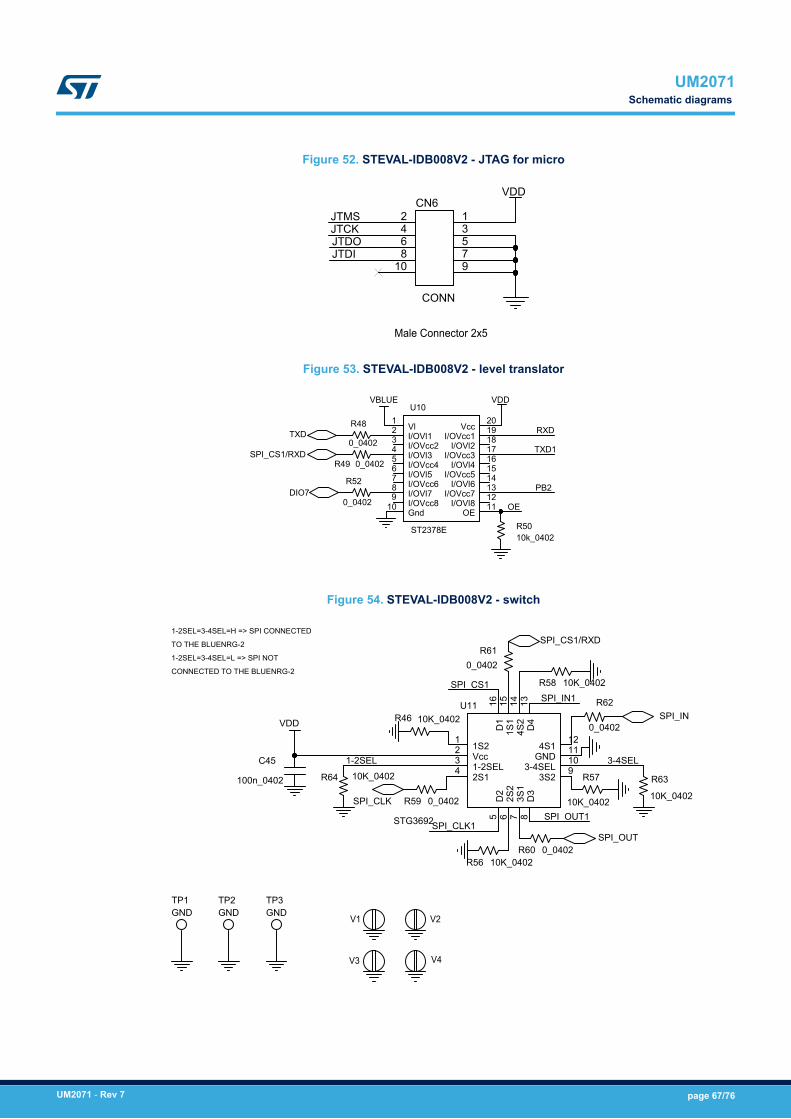
Figure 52. STEVAL-IDB008V2 - JTAG for micro
Male Connector 2x5
JTMSJTCKJTDOJTDI
VDDCN6
CONN
12345678910
Figure 53. STEVAL-IDB008V2 - level translator
OE
RXD
TXD1
PB2
TXD
SPI_CS1/RXD
DIO7
VDDVBLUE
R48
0_0402
U10
ST2378E
Vl1
I/OVl12
I/OVcc23
I/OVl34
I/OVcc45
I/OVl56
I/OVcc67
I/OVl78
I/OVcc89
Gnd10
Vcc20
I/OVcc119
I/OVl218
I/OVcc317
I/OVl416
I/OVcc515
I/OVl614
I/OVcc713
I/OVl812
OE11
R5010k_0402
R52
0_0402
R49 0_0402
Figure 54. STEVAL-IDB008V2 - switch
V1 V2
V3 V4
1-2SEL=3-4SEL=H => SPI CONNECTED
TO THE BLUENRG-2
1-2SEL=3-4SEL=L => SPI NOT
CONNECTED TO THE BLUENRG-2
1-2SEL
SPI_CS1
SPI_CLK1SPI_OUT1
SPI_IN1
3-4SEL
SPI_IN
SPI_OUT
SPI_CLK
SPI_CS1/RXD
VDD
R59 0_0402
R63
10K_0402
R610_0402
R58 10K_0402
R56 10K_0402
U11
STG3692
1S21
Vcc2
1-2SEL3
2S14
D2
5
2S2
6
3S1
7
D3
8
D1
16
1S1
15
4S2
14
D4
13
4S112
GND11
3-4SEL10
3S29
TP1GND
C45
100n_0402
R60 0_0402
R64 10K_0402 R57
10K_0402
R62
0_0402
TP3GND
R46 10K_0402
TP2GND
UM2071Schematic diagrams
UM2071 - Rev 7 page 67/76

Revision history
Table 10. Document revision history
Date Version Changes
06-Jun-2016 1 Initial release.
08-Nov-2016 2 Added Section 11: "BlueNRG-1 sensor profile central demo" and description for ADC DMA, PDM andMFT timers.
23-Dec-2016 3 Updated STEVAL-IDB007V1 development platform and STEVAL-IDB007V1 board components.
27-Jun-2017 4
Updated: Figure 10: "BLE demonstration and test applications", and Section 18.9: " SPI examples ".Added: Section 16: "BLE security demonstration applications", Section 17: "BLE power consumptiondemo application", Section 18.6: "Public Key Accelerator (PKA) demonstration application" andSection 18.7: "RNG examples". Added reference to BlueNRG-2 device and related SW components.Add reference to STEVAL-IDB008V1 kit and related schematics pictures.
17-Oct-2017 5 Added reference to BlueNRG-1-V1 DK SW package supporting BLE stack v1.x family.
17-Jan-2018 6 Added references to STEVAL-IDB007V2, STEVAL-IDB008V2 platforms and related schematics.
08-Jun-2018 7
Updated Figure 7. BlueNRG-1 Navigator, Figure 8. BLE Beacon application, Figure 9. BLE BeaconFlash programming, Figure 11. Basic examples, Figure 12. BLE demonstration and test applications,Figure 13. Peripherals driver examples, Figure 15. STEVAL-IDB007V2 kit components, Figure16. BlueNRG-1 radio parameters wizard, Section 5.1 Software directory structure, Section 6.1.3Entering non-connectable mode , Section 13.2 BLE bidirectional throughput scenario, Section18.9 RTC examples , Section 18.13 UART examples and Section 19 Schematic diagrams.
Added Section 2.11 Integrated balun with matching network and harmonics filter, Section 3.1.4 BlueNRG-1 Navigator ‘2.4 GHz radio proprietary examples’, Section 17 BLE master and slavemultiple connection demonstration application, Section 17.1 Application roles, Section17.1.1 Master_Slave device role and Section 18.7 2.4 GHz radio proprietary examples.
Removed BlueNRG-1 Flasher utility section.
UM2071
UM2071 - Rev 7 page 68/76
Contents
1 Getting started . . . . . . . . . . . . . . . . . . . . . . . . . . . . . . . . . . . . . . . . . . . . . . . . . . . . . . . . . . . . . . . . . . . .2
1.1 Kit contents . . . . . . . . . . . . . . . . . . . . . . . . . . . . . . . . . . . . . . . . . . . . . . . . . . . . . . . . . . . . . . . . . . . 2
1.2 System requirements . . . . . . . . . . . . . . . . . . . . . . . . . . . . . . . . . . . . . . . . . . . . . . . . . . . . . . . . . . . 2
1.3 BlueNRG-1, BlueNRG-2 development kits setup . . . . . . . . . . . . . . . . . . . . . . . . . . . . . . . . . . . . 2
2 Hardware description . . . . . . . . . . . . . . . . . . . . . . . . . . . . . . . . . . . . . . . . . . . . . . . . . . . . . . . . . . . . . .3
2.1 STEVAL-IDB007Vx/STEVAL-IDB008Vx boards overview . . . . . . . . . . . . . . . . . . . . . . . . . . . . . 3
2.2 BlueNRG-1, BlueNRG-2 SoC connections . . . . . . . . . . . . . . . . . . . . . . . . . . . . . . . . . . . . . . . . . 4
2.3 Power supply . . . . . . . . . . . . . . . . . . . . . . . . . . . . . . . . . . . . . . . . . . . . . . . . . . . . . . . . . . . . . . . . . . 6
2.4 Jumpers . . . . . . . . . . . . . . . . . . . . . . . . . . . . . . . . . . . . . . . . . . . . . . . . . . . . . . . . . . . . . . . . . . . . . 7
2.5 Sensors . . . . . . . . . . . . . . . . . . . . . . . . . . . . . . . . . . . . . . . . . . . . . . . . . . . . . . . . . . . . . . . . . . . . . . 7
2.6 Extension connector . . . . . . . . . . . . . . . . . . . . . . . . . . . . . . . . . . . . . . . . . . . . . . . . . . . . . . . . . . . 7
2.7 Push-buttons . . . . . . . . . . . . . . . . . . . . . . . . . . . . . . . . . . . . . . . . . . . . . . . . . . . . . . . . . . . . . . . . . . 7
2.8 JTAG connector. . . . . . . . . . . . . . . . . . . . . . . . . . . . . . . . . . . . . . . . . . . . . . . . . . . . . . . . . . . . . . . . 7
2.9 LEDs . . . . . . . . . . . . . . . . . . . . . . . . . . . . . . . . . . . . . . . . . . . . . . . . . . . . . . . . . . . . . . . . . . . . . . . . 8
2.10 STM32L151CBU6 microcontroller . . . . . . . . . . . . . . . . . . . . . . . . . . . . . . . . . . . . . . . . . . . . . . . . 8
2.11 Integrated balun with matching network and harmonics filter . . . . . . . . . . . . . . . . . . . . . . . . . . 8
2.12 Current measurements . . . . . . . . . . . . . . . . . . . . . . . . . . . . . . . . . . . . . . . . . . . . . . . . . . . . . . . . . 8
2.13 Hardware setup . . . . . . . . . . . . . . . . . . . . . . . . . . . . . . . . . . . . . . . . . . . . . . . . . . . . . . . . . . . . . . . . 8
3 BlueNRG-1, BlueNRG-2 Navigator. . . . . . . . . . . . . . . . . . . . . . . . . . . . . . . . . . . . . . . . . . . . . . . . . .9
3.1 BlueNRG-1 Navigator ‘Demonstration Applications’ . . . . . . . . . . . . . . . . . . . . . . . . . . . . . . . . . 9
3.1.1 BlueNRG-1 Navigator ‘Basic examples’ . . . . . . . . . . . . . . . . . . . . . . . . . . . . . . . . . . . . . 11
3.1.2 BlueNRG-1 Navigator ‘BLE demonstration and test applications’ . . . . . . . . . . . . . . . . . . . 11
3.1.3 BlueNRG-1 Navigator ‘Peripherals driver examples’ . . . . . . . . . . . . . . . . . . . . . . . . . . . . 12
3.1.4 BlueNRG-1 Navigator ‘2.4 GHz radio proprietary examples’ . . . . . . . . . . . . . . . . . . . . . . 12
3.2 BlueNRG-1 Navigator ‘Development Kits’ . . . . . . . . . . . . . . . . . . . . . . . . . . . . . . . . . . . . . . . . . 13
3.2.1 BlueNRG-1 Navigator ‘Release Notes’ and ‘License’ . . . . . . . . . . . . . . . . . . . . . . . . . . . 13
4 BlueNRG-1 radio parameters wizard . . . . . . . . . . . . . . . . . . . . . . . . . . . . . . . . . . . . . . . . . . . . . .14
4.1 How to run . . . . . . . . . . . . . . . . . . . . . . . . . . . . . . . . . . . . . . . . . . . . . . . . . . . . . . . . . . . . . . . . . . . 14
4.2 Main user interface window . . . . . . . . . . . . . . . . . . . . . . . . . . . . . . . . . . . . . . . . . . . . . . . . . . . . . 14
UM2071Contents
UM2071 - Rev 7 page 69/76
5 Programming with BlueNRG-1, BlueNRG-2 system on chip . . . . . . . . . . . . . . . . . . . . . . . .16
5.1 Software directory structure . . . . . . . . . . . . . . . . . . . . . . . . . . . . . . . . . . . . . . . . . . . . . . . . . . . . . 16
6 BLE beacon demonstration application . . . . . . . . . . . . . . . . . . . . . . . . . . . . . . . . . . . . . . . . . .17
6.1 BLE Beacon application setup . . . . . . . . . . . . . . . . . . . . . . . . . . . . . . . . . . . . . . . . . . . . . . . . . . 17
6.1.1 Initialization . . . . . . . . . . . . . . . . . . . . . . . . . . . . . . . . . . . . . . . . . . . . . . . . . . . . . . . . . . . 17
6.1.2 Define advertising data . . . . . . . . . . . . . . . . . . . . . . . . . . . . . . . . . . . . . . . . . . . . . . . . . . 17
6.1.3 Entering non-connectable mode . . . . . . . . . . . . . . . . . . . . . . . . . . . . . . . . . . . . . . . . . . . 17
7 BLE chat demo application . . . . . . . . . . . . . . . . . . . . . . . . . . . . . . . . . . . . . . . . . . . . . . . . . . . . . . .19
7.1 Peripheral and central device setup . . . . . . . . . . . . . . . . . . . . . . . . . . . . . . . . . . . . . . . . . . . . . 19
7.1.1 Initialization . . . . . . . . . . . . . . . . . . . . . . . . . . . . . . . . . . . . . . . . . . . . . . . . . . . . . . . . . . . . 19
7.1.2 Add service and characteristics . . . . . . . . . . . . . . . . . . . . . . . . . . . . . . . . . . . . . . . . . . . . 20
7.1.3 Enter connectable mode . . . . . . . . . . . . . . . . . . . . . . . . . . . . . . . . . . . . . . . . . . . . . . . . . 20
7.1.4 Connection with central device . . . . . . . . . . . . . . . . . . . . . . . . . . . . . . . . . . . . . . . . . . . . 20
8 BLE chat master and slave demo application. . . . . . . . . . . . . . . . . . . . . . . . . . . . . . . . . . . . . .22
8.1 BLE chat master and slave roles. . . . . . . . . . . . . . . . . . . . . . . . . . . . . . . . . . . . . . . . . . . . . . . . . 22
8.1.1 Initialization . . . . . . . . . . . . . . . . . . . . . . . . . . . . . . . . . . . . . . . . . . . . . . . . . . . . . . . . . . . . 22
8.1.2 Add service and characteristics . . . . . . . . . . . . . . . . . . . . . . . . . . . . . . . . . . . . . . . . . . . . 22
8.1.3 Start discovery procedure . . . . . . . . . . . . . . . . . . . . . . . . . . . . . . . . . . . . . . . . . . . . . . . . . 22
8.1.4 Enter connectable mode . . . . . . . . . . . . . . . . . . . . . . . . . . . . . . . . . . . . . . . . . . . . . . . . . 23
8.1.5 Connection with chat master and slave client device. . . . . . . . . . . . . . . . . . . . . . . . . . . . . 23
9 BLE remote control demo application . . . . . . . . . . . . . . . . . . . . . . . . . . . . . . . . . . . . . . . . . . . . .24
9.1 BLE remote control application setup . . . . . . . . . . . . . . . . . . . . . . . . . . . . . . . . . . . . . . . . . . . . 24
9.1.1 Initialization . . . . . . . . . . . . . . . . . . . . . . . . . . . . . . . . . . . . . . . . . . . . . . . . . . . . . . . . . . . . 24
9.1.2 Define advertising data . . . . . . . . . . . . . . . . . . . . . . . . . . . . . . . . . . . . . . . . . . . . . . . . . . 24
9.1.3 Add service and characteristics . . . . . . . . . . . . . . . . . . . . . . . . . . . . . . . . . . . . . . . . . . . . 25
9.1.4 Connection with a BLE Central device . . . . . . . . . . . . . . . . . . . . . . . . . . . . . . . . . . . . . . . 25
10 BLE sensor profile demo . . . . . . . . . . . . . . . . . . . . . . . . . . . . . . . . . . . . . . . . . . . . . . . . . . . . . . . . .26
10.1 BlueNRG app for smartphones . . . . . . . . . . . . . . . . . . . . . . . . . . . . . . . . . . . . . . . . . . . . . . . . . . 26
10.2 BLE sensor profile demo: connection with a central device. . . . . . . . . . . . . . . . . . . . . . . . . . . 27
10.2.1 Initialization . . . . . . . . . . . . . . . . . . . . . . . . . . . . . . . . . . . . . . . . . . . . . . . . . . . . . . . . . . . . 27
10.2.2 Add service and characteristics. . . . . . . . . . . . . . . . . . . . . . . . . . . . . . . . . . . . . . . . . . . . . 27
UM2071Contents
UM2071 - Rev 7 page 70/76
10.2.3 Enter connectable mode . . . . . . . . . . . . . . . . . . . . . . . . . . . . . . . . . . . . . . . . . . . . . . . . . 28
10.2.4 Connection with central device . . . . . . . . . . . . . . . . . . . . . . . . . . . . . . . . . . . . . . . . . . . . . 28
11 BLE sensor profile center demo. . . . . . . . . . . . . . . . . . . . . . . . . . . . . . . . . . . . . . . . . . . . . . . . . . .29
12 BLE HID/HOGP demonstration application . . . . . . . . . . . . . . . . . . . . . . . . . . . . . . . . . . . . . . . .30
12.1 BLE HID/HOGP mouse demonstration application. . . . . . . . . . . . . . . . . . . . . . . . . . . . . . . . . . 30
12.2 BLE HID/HOGP keyboard demonstration application. . . . . . . . . . . . . . . . . . . . . . . . . . . . . . . . 30
13 BLE throughput demonstration application . . . . . . . . . . . . . . . . . . . . . . . . . . . . . . . . . . . . . . .31
13.1 BLE unidirectional throughput scenario . . . . . . . . . . . . . . . . . . . . . . . . . . . . . . . . . . . . . . . . . . . 31
13.2 BLE bidirectional throughput scenario . . . . . . . . . . . . . . . . . . . . . . . . . . . . . . . . . . . . . . . . . . . . 31
14 BLE notification consumer demonstration application. . . . . . . . . . . . . . . . . . . . . . . . . . . . .33
15 BLE security demonstration applications . . . . . . . . . . . . . . . . . . . . . . . . . . . . . . . . . . . . . . . . .34
15.1 Peripheral device. . . . . . . . . . . . . . . . . . . . . . . . . . . . . . . . . . . . . . . . . . . . . . . . . . . . . . . . . . . . . . 34
15.2 Central device . . . . . . . . . . . . . . . . . . . . . . . . . . . . . . . . . . . . . . . . . . . . . . . . . . . . . . . . . . . . . . . . 35
16 BLE power consumption demo application. . . . . . . . . . . . . . . . . . . . . . . . . . . . . . . . . . . . . . . .37
17 BLE master and slave multiple connection demonstration application . . . . . . . . . . . . .38
17.1 Application roles . . . . . . . . . . . . . . . . . . . . . . . . . . . . . . . . . . . . . . . . . . . . . . . . . . . . . . . . . . . . . . 38
17.1.1 Master_Slave device role . . . . . . . . . . . . . . . . . . . . . . . . . . . . . . . . . . . . . . . . . . . . . . . . . 38
17.1.2 Master role . . . . . . . . . . . . . . . . . . . . . . . . . . . . . . . . . . . . . . . . . . . . . . . . . . . . . . . . . . . . 38
18 BlueNRG-1, BlueNRG-2 peripheral driver examples . . . . . . . . . . . . . . . . . . . . . . . . . . . . . . .40
18.1 ADC examples. . . . . . . . . . . . . . . . . . . . . . . . . . . . . . . . . . . . . . . . . . . . . . . . . . . . . . . . . . . . . . . . 40
18.2 Flash example . . . . . . . . . . . . . . . . . . . . . . . . . . . . . . . . . . . . . . . . . . . . . . . . . . . . . . . . . . . . . . . . 40
18.3 GPIO examples . . . . . . . . . . . . . . . . . . . . . . . . . . . . . . . . . . . . . . . . . . . . . . . . . . . . . . . . . . . . . . . 40
18.4 I²C examples . . . . . . . . . . . . . . . . . . . . . . . . . . . . . . . . . . . . . . . . . . . . . . . . . . . . . . . . . . . . . . . . 41
18.5 Micro examples . . . . . . . . . . . . . . . . . . . . . . . . . . . . . . . . . . . . . . . . . . . . . . . . . . . . . . . . . . . . . . 41
18.6 Public Key Accelerator (PKA) demonstration application. . . . . . . . . . . . . . . . . . . . . . . . . . . . . 41
18.7 2.4 GHz radio proprietary examples . . . . . . . . . . . . . . . . . . . . . . . . . . . . . . . . . . . . . . . . . . . . . . 42
18.8 RNG examples . . . . . . . . . . . . . . . . . . . . . . . . . . . . . . . . . . . . . . . . . . . . . . . . . . . . . . . . . . . . . . . 42
18.9 RTC examples . . . . . . . . . . . . . . . . . . . . . . . . . . . . . . . . . . . . . . . . . . . . . . . . . . . . . . . . . . . . . . . 42
18.10 SPI examples . . . . . . . . . . . . . . . . . . . . . . . . . . . . . . . . . . . . . . . . . . . . . . . . . . . . . . . . . . . . . . . 43
18.11 SysTick examples . . . . . . . . . . . . . . . . . . . . . . . . . . . . . . . . . . . . . . . . . . . . . . . . . . . . . . . . . . . . 43
UM2071Contents
UM2071 - Rev 7 page 71/76
18.12 Timers examples . . . . . . . . . . . . . . . . . . . . . . . . . . . . . . . . . . . . . . . . . . . . . . . . . . . . . . . . . . . . . . 43
18.13 UART examples . . . . . . . . . . . . . . . . . . . . . . . . . . . . . . . . . . . . . . . . . . . . . . . . . . . . . . . . . . . . . . 45
18.14 WDG examples . . . . . . . . . . . . . . . . . . . . . . . . . . . . . . . . . . . . . . . . . . . . . . . . . . . . . . . . . . . . . . 45
19 Schematic diagrams . . . . . . . . . . . . . . . . . . . . . . . . . . . . . . . . . . . . . . . . . . . . . . . . . . . . . . . . . . . . . .46
Revision history . . . . . . . . . . . . . . . . . . . . . . . . . . . . . . . . . . . . . . . . . . . . . . . . . . . . . . . . . . . . . . . . . . . . . . .68
UM2071Contents
UM2071 - Rev 7 page 72/76
List of figuresFigure 1. STEVAL-IDB007V1 development platform . . . . . . . . . . . . . . . . . . . . . . . . . . . . . . . . . . . . . . . . . . . . . . . . . 1Figure 2. STEVAL-IDB007V2 development platform . . . . . . . . . . . . . . . . . . . . . . . . . . . . . . . . . . . . . . . . . . . . . . . . . 1Figure 3. STEVAL-IDB008V1 development platform . . . . . . . . . . . . . . . . . . . . . . . . . . . . . . . . . . . . . . . . . . . . . . . . . 1Figure 4. STEVAL-IDB008V2 development platform . . . . . . . . . . . . . . . . . . . . . . . . . . . . . . . . . . . . . . . . . . . . . . . . . 1Figure 5. STEVAL-IDB007Vx board components . . . . . . . . . . . . . . . . . . . . . . . . . . . . . . . . . . . . . . . . . . . . . . . . . . . 3Figure 6. STEVAL-IDB008Vx board components . . . . . . . . . . . . . . . . . . . . . . . . . . . . . . . . . . . . . . . . . . . . . . . . . . . 4Figure 7. BlueNRG-1 Navigator . . . . . . . . . . . . . . . . . . . . . . . . . . . . . . . . . . . . . . . . . . . . . . . . . . . . . . . . . . . . . . . 9Figure 8. BLE Beacon application. . . . . . . . . . . . . . . . . . . . . . . . . . . . . . . . . . . . . . . . . . . . . . . . . . . . . . . . . . . . . 10Figure 9. BLE Beacon Flash programming. . . . . . . . . . . . . . . . . . . . . . . . . . . . . . . . . . . . . . . . . . . . . . . . . . . . . . . 10Figure 10. BLE Beacon documentation . . . . . . . . . . . . . . . . . . . . . . . . . . . . . . . . . . . . . . . . . . . . . . . . . . . . . . . . . . 11Figure 11. Basic examples . . . . . . . . . . . . . . . . . . . . . . . . . . . . . . . . . . . . . . . . . . . . . . . . . . . . . . . . . . . . . . . . . . 11Figure 12. BLE demonstration and test applications . . . . . . . . . . . . . . . . . . . . . . . . . . . . . . . . . . . . . . . . . . . . . . . . . 12Figure 13. Peripherals driver examples . . . . . . . . . . . . . . . . . . . . . . . . . . . . . . . . . . . . . . . . . . . . . . . . . . . . . . . . . . 12Figure 14. 2.4 GHz radio proprietary examples . . . . . . . . . . . . . . . . . . . . . . . . . . . . . . . . . . . . . . . . . . . . . . . . . . . . 13Figure 15. STEVAL-IDB007V2 kit components. . . . . . . . . . . . . . . . . . . . . . . . . . . . . . . . . . . . . . . . . . . . . . . . . . . . . 13Figure 16. BlueNRG-1 radio parameters wizard . . . . . . . . . . . . . . . . . . . . . . . . . . . . . . . . . . . . . . . . . . . . . . . . . . . . 14Figure 17. BLE chat client . . . . . . . . . . . . . . . . . . . . . . . . . . . . . . . . . . . . . . . . . . . . . . . . . . . . . . . . . . . . . . . . . . . 21Figure 18. BLE chat server . . . . . . . . . . . . . . . . . . . . . . . . . . . . . . . . . . . . . . . . . . . . . . . . . . . . . . . . . . . . . . . . . . 21Figure 19. BLE sensor demo GATT database . . . . . . . . . . . . . . . . . . . . . . . . . . . . . . . . . . . . . . . . . . . . . . . . . . . . . 26Figure 20. BlueNRG sensor app . . . . . . . . . . . . . . . . . . . . . . . . . . . . . . . . . . . . . . . . . . . . . . . . . . . . . . . . . . . . . . 27Figure 21. STEVAL-IDB007V1 Arduino connectors. . . . . . . . . . . . . . . . . . . . . . . . . . . . . . . . . . . . . . . . . . . . . . . . . . 46Figure 22. STEVAL-IDB007V1 JTAG . . . . . . . . . . . . . . . . . . . . . . . . . . . . . . . . . . . . . . . . . . . . . . . . . . . . . . . . . . . 46Figure 23. STEVAL-IDB007V1 BlueNRG-1 . . . . . . . . . . . . . . . . . . . . . . . . . . . . . . . . . . . . . . . . . . . . . . . . . . . . . . . 47Figure 24. STEVAL-IDB007V1 power management, sensors . . . . . . . . . . . . . . . . . . . . . . . . . . . . . . . . . . . . . . . . . . . 48Figure 25. STEVAL-IDB007V1 buttons and LEDs . . . . . . . . . . . . . . . . . . . . . . . . . . . . . . . . . . . . . . . . . . . . . . . . . . . 49Figure 26. STEVAL-IDB007V1 micro . . . . . . . . . . . . . . . . . . . . . . . . . . . . . . . . . . . . . . . . . . . . . . . . . . . . . . . . . . . 50Figure 27. STEVAL-IDB007V1 USB, level translator, JTAG for micro. . . . . . . . . . . . . . . . . . . . . . . . . . . . . . . . . . . . . . 51Figure 28. STEVAL-IDB007V1 switch . . . . . . . . . . . . . . . . . . . . . . . . . . . . . . . . . . . . . . . . . . . . . . . . . . . . . . . . . . . 52Figure 29. STEVAL-IDB008V1 circuit schematic JTAG . . . . . . . . . . . . . . . . . . . . . . . . . . . . . . . . . . . . . . . . . . . . . . . 52Figure 30. STEVAL-IDB008V1 circuit schematic Arduino connectors . . . . . . . . . . . . . . . . . . . . . . . . . . . . . . . . . . . . . 53Figure 31. STEVAL-IDB008V1 BlueNRG-2 . . . . . . . . . . . . . . . . . . . . . . . . . . . . . . . . . . . . . . . . . . . . . . . . . . . . . . . 54Figure 32. STEVAL-IDB008V1 buttons and LEDs . . . . . . . . . . . . . . . . . . . . . . . . . . . . . . . . . . . . . . . . . . . . . . . . . . . 55Figure 33. STEVAL-IDB008V1 sensors . . . . . . . . . . . . . . . . . . . . . . . . . . . . . . . . . . . . . . . . . . . . . . . . . . . . . . . . . . 56Figure 34. STEVAL-IDB008V1 power management . . . . . . . . . . . . . . . . . . . . . . . . . . . . . . . . . . . . . . . . . . . . . . . . . 57Figure 35. STEVAL-IDB008V1 JTAG for micro . . . . . . . . . . . . . . . . . . . . . . . . . . . . . . . . . . . . . . . . . . . . . . . . . . . . . 57Figure 36. STEVAL-IDB008V1 USB . . . . . . . . . . . . . . . . . . . . . . . . . . . . . . . . . . . . . . . . . . . . . . . . . . . . . . . . . . . . 58Figure 37. STEVAL-IDB008V1 circuit schematic TP1, TP2, TP3. . . . . . . . . . . . . . . . . . . . . . . . . . . . . . . . . . . . . . . . . 58Figure 38. STEVAL-IDB008V1 switch . . . . . . . . . . . . . . . . . . . . . . . . . . . . . . . . . . . . . . . . . . . . . . . . . . . . . . . . . . . 58Figure 39. STEVAL-IDB008V1 micro . . . . . . . . . . . . . . . . . . . . . . . . . . . . . . . . . . . . . . . . . . . . . . . . . . . . . . . . . . . 59Figure 40. STEVAL-IDB008V1 level translator . . . . . . . . . . . . . . . . . . . . . . . . . . . . . . . . . . . . . . . . . . . . . . . . . . . . . 59Figure 41. STEVAL-IDB007V2 - scheme 1 . . . . . . . . . . . . . . . . . . . . . . . . . . . . . . . . . . . . . . . . . . . . . . . . . . . . . . . 60Figure 42. STEVAL-IDB007V2 - scheme 2 . . . . . . . . . . . . . . . . . . . . . . . . . . . . . . . . . . . . . . . . . . . . . . . . . . . . . . . 61Figure 43. STEVAL-IDB007V2 - scheme 3 . . . . . . . . . . . . . . . . . . . . . . . . . . . . . . . . . . . . . . . . . . . . . . . . . . . . . . . 61Figure 44. STEVAL-IDB008V2 - JTAG . . . . . . . . . . . . . . . . . . . . . . . . . . . . . . . . . . . . . . . . . . . . . . . . . . . . . . . . . . 62Figure 45. STEVAL-IDB008V2 - Arduino connection . . . . . . . . . . . . . . . . . . . . . . . . . . . . . . . . . . . . . . . . . . . . . . . . 62Figure 46. STEVAL-IDB008V2 circuit schematic . . . . . . . . . . . . . . . . . . . . . . . . . . . . . . . . . . . . . . . . . . . . . . . . . . . 63Figure 47. STEVAL-IDB008V2 - power management . . . . . . . . . . . . . . . . . . . . . . . . . . . . . . . . . . . . . . . . . . . . . . . . 63Figure 48. STEVAL-IDB008V2 - Sensors. . . . . . . . . . . . . . . . . . . . . . . . . . . . . . . . . . . . . . . . . . . . . . . . . . . . . . . . . 64Figure 49. STEVAL-IDB008V2 - buttons and LEDs . . . . . . . . . . . . . . . . . . . . . . . . . . . . . . . . . . . . . . . . . . . . . . . . . . 65Figure 50. STEVAL-IDB008V2 - micro . . . . . . . . . . . . . . . . . . . . . . . . . . . . . . . . . . . . . . . . . . . . . . . . . . . . . . . . . . 66Figure 51. STEVAL-IDB008V2 - USB . . . . . . . . . . . . . . . . . . . . . . . . . . . . . . . . . . . . . . . . . . . . . . . . . . . . . . . . . . . 66Figure 52. STEVAL-IDB008V2 - JTAG for micro . . . . . . . . . . . . . . . . . . . . . . . . . . . . . . . . . . . . . . . . . . . . . . . . . . . . 67
UM2071List of figures
UM2071 - Rev 7 page 73/76
Figure 53. STEVAL-IDB008V2 - level translator . . . . . . . . . . . . . . . . . . . . . . . . . . . . . . . . . . . . . . . . . . . . . . . . . . . . 67Figure 54. STEVAL-IDB008V2 - switch . . . . . . . . . . . . . . . . . . . . . . . . . . . . . . . . . . . . . . . . . . . . . . . . . . . . . . . . . . 67
UM2071List of figures
UM2071 - Rev 7 page 74/76
List of tablesTable 1. STEVAL-IDB007Vx/STEVAL-IDB008Vx board component descriptions. . . . . . . . . . . . . . . . . . . . . . . . . . . . . . . 4Table 2. BlueNRG-1, BlueNRG-2 pins description with board functions . . . . . . . . . . . . . . . . . . . . . . . . . . . . . . . . . . . . . 5Table 3. STEVAL-IDB007V1, STEVAL-IDB008V1 kits platforms power supply modes . . . . . . . . . . . . . . . . . . . . . . . . . . . 7Table 4. STEVAL-IDB007Vx, STEVAL-IDB008Vx kits platforms jumpers . . . . . . . . . . . . . . . . . . . . . . . . . . . . . . . . . . . . 7Table 5. BlueNRG-1 Beacon advertising manufacturing data . . . . . . . . . . . . . . . . . . . . . . . . . . . . . . . . . . . . . . . . . . . 17Table 6. Serial port configuration . . . . . . . . . . . . . . . . . . . . . . . . . . . . . . . . . . . . . . . . . . . . . . . . . . . . . . . . . . . . . . 19Table 7. BLE remote advertising data . . . . . . . . . . . . . . . . . . . . . . . . . . . . . . . . . . . . . . . . . . . . . . . . . . . . . . . . . . . 24Table 8. BLE security demonstration applications security configurations combinations . . . . . . . . . . . . . . . . . . . . . . . . . 34Table 9. Peripheral device advertising local name parameter value. . . . . . . . . . . . . . . . . . . . . . . . . . . . . . . . . . . . . . . 34Table 10. Document revision history . . . . . . . . . . . . . . . . . . . . . . . . . . . . . . . . . . . . . . . . . . . . . . . . . . . . . . . . . . . . . 68
UM2071List of tables
UM2071 - Rev 7 page 75/76

IMPORTANT NOTICE – PLEASE READ CAREFULLY
STMicroelectronics NV and its subsidiaries (“ST”) reserve the right to make changes, corrections, enhancements, modifications, and improvements to STproducts and/or to this document at any time without notice. Purchasers should obtain the latest relevant information on ST products before placing orders. STproducts are sold pursuant to ST’s terms and conditions of sale in place at the time of order acknowledgement.
Purchasers are solely responsible for the choice, selection, and use of ST products and ST assumes no liability for application assistance or the design ofPurchasers’ products.
No license, express or implied, to any intellectual property right is granted by ST herein.
Resale of ST products with provisions different from the information set forth herein shall void any warranty granted by ST for such product.
ST and the ST logo are trademarks of ST. All other product or service names are the property of their respective owners.
Information in this document supersedes and replaces information previously supplied in any prior versions of this document.
© 2018 STMicroelectronics – All rights reserved
UM2071
UM2071 - Rev 7 page 76/76