bond strength characterization of su-8 to su-8 for
TRANSCRIPT
Bond Strength Characterization of SU-8 to SU-8 for Fabricating Microchannels of an
Electrokinetic Microfluidic Pump
A Senior Project Presented to
the Faculty of California Polytechnic State University,
San Luis Obispo
In Partial Fulfilment of the Requirements
for the Degree Bachelor of Science in Engineering,
With a Specialization in Materials Engineering
By
Nash Anderson
Advisor: Dr. Richard Savage
May 31, 2012

ii
© 2012
Nash Anderson
ALL RIGHTS RESERVED

iii
Approval Page
Project Title: BOND STRENGTH CHARACTERIZATION OF SU-8 TO SU-8 FOR
FABRICATING MICROCHANNELS OF AN ELECTROKINETIC
MICROFLUIDIC PUMP
Author: Nash Anderson
Date Submitted: May 31, 2012
CAL POLY STATE UNIVERSITY
Materials Engineering Department
Since this project is a result of a class assignment, it has been graded and accepted as fulfillment
of the course requirements. Acceptance does not imply technical accuracy or reliability. Any use
of the information in this report, including numerical data, is done at the risk of the user. These
risks may include catastrophic failure of the device or infringement of patent or copyright laws.
The students, faculty, and staff of Cal Poly State University, San Luis Obispo cannot be held
liable for any misuse of the project.
Prof. Richard Savage ____________________________
Faculty Advisor Signature
Prof. Trevor Harding ____________________________
Department Chair Signature

iv
Abstract
BOND STRENGTH CHARACTERIZATION OF SU-8 TO SU-8 FOR FABRICATING
MICROCHANNELS OF AN ELECTROKINETIC MICROFLUIDIC PUMP
Photosensitive negative resist polymer layers of SU-8 2050 were adhered to 100 mm n-type
silicon and Pyrex wafers via spin coating. These wafers were then bonded together at various
temperatures of 100 �C, 120 �C, 140 �C, 150 �C, 160 �C, and 180 �C. The target thickness
of each SU-8 layer was 100 µm. Photolithography was used to create microfluidic channels within
the SU-8. An n-type silicon wafer and a Pyrex wafer, each with an SU-8 layer, were brought
together on the “hard bake” or final step of SU-8 polymerization. A pressure of ~300 KPa was
applied during the hard bake for 20 minutes. The apparatus was left under pressure to cool to
room temperature. A JEOL JSM-6390 SEM and optical microscopy were used to observe effects
on channels to determine if the hard bake temperature caused deterioration of channel walls or
an incomplete bond. Void formation was avoided by drilling fluid input and output holes through
Pyrex wafer prior to wafer bonding processes, allowing air and solvent release points while under
heat and pressure treatment. Tensile testing was performed on partially overlapped wafers by
pulling them apart to quantify the bond strength at stated temperatures. The bond temperature
with the strongest SU-8 to SU-8 bond that withheld channel integrity will be used for electrokinetic
microfluidic pumping thesis analysis of buffer solutions ranging from pH 2 to 12.

v
Table of Contents
Approval Page ................................................................................................................... iii
Abstract ............................................................................................................................ iv
List of Tables .................................................................................................................... vii
List of Equations .............................................................................................................. viii
List of Figures .................................................................................................................... ix
Keywords .......................................................................................................................... xi
1. Introduction ............................................................................................................................. 1
1.1. Problem Statement .............................................................................................................. 1
1.2. Project Scope ....................................................................................................................... 1
1.3. Materials Selection .............................................................................................................. 2
1.4. Broader Impacts ................................................................................................................... 2
1.4.1. Health and Safety ............................................................................................................. 2
1.4.2. Environmental Factors ..................................................................................................... 3
1.5. Background .......................................................................................................................... 3
1.5.1. Microfluidics..................................................................................................................... 3
1.5.2. SU-8 .................................................................................................................................. 4
1.5.3. Electrokinetics .................................................................................................................. 6
1.5.4. Electroosmotic Flow ......................................................................................................... 7
2. Experimental Procedures ........................................................................................................ 9
2.1. Mechanical Drilling of Fluid Input/Output Holes Through Pyrex Wafer ............................ 11
2.2. Silicon & Pyrex Wafer Clean and Dehydration................................................................... 11
2.3. Spin Coating of SU-8 .......................................................................................................... 12
2.4. Soft Bake ............................................................................................................................ 13
2.5. Exposure and Post Exposure Bake ..................................................................................... 14
2.6. Development...................................................................................................................... 18
2.7. Pre-Bond ............................................................................................................................ 18
2.8. Bond Bake .......................................................................................................................... 19
2.9. PDMS Microfluidic Hookup ................................................................................................ 20
3. Results & Discussion of Bonding Processes .......................................................................... 21
3.1. Silicon to Silicon Wafer Bonding ........................................................................................ 21

vi
3.2. Silicon to Pyrex Wafer Bonding .......................................................................................... 25
4. Conclusions and Continuation of Project ............................................................................. 29
4.1. Changes to Procedures ...................................................................................................... 29
4.2. Continuation of Project ...................................................................................................... 29
References ..................................................................................................................................... 31

vii
List of Tables
Table I. SU-8 to SU-8 bond processing steps. Step 1 & 9 are neglected for silicon to silicon
bonding procedures. ................................................................................................................... 11
Table II. Results of Silicon to Silicon wafer bond quality and SU-8 ....................................... 22

viii
List of Equations
Equation 1. Equation to determine Reynolds number. ρ = fluid density, V = velocity, D =
characteristic length, µ = dynamic viscosity of fluid. ................................................................ 4

ix
List of Figures
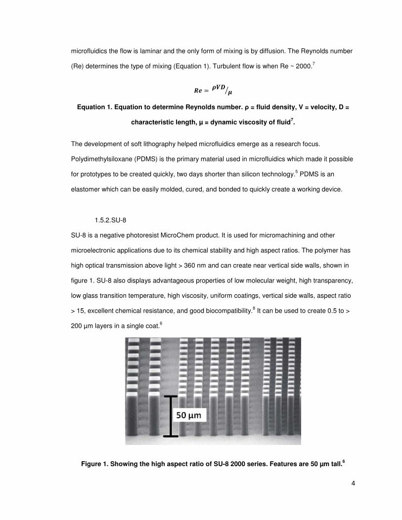
Figure 1. Showing the high aspect ratio of SU-8 2000 series. Features are 50 µm tall.6 ........ 4
Figure 2. Representative SU-8 molecule which has on average 8 epoxy groups. Prior to
exposure.8 ....................................................................................................................................... 5
Figure 3. Chemical reaction that takes place during photolithography exposure.8 ............... 6
Figure 4. Cross linking process which starts during the Post Exposure Bake (PEB).8 ......... 6
Figure 5. Velocity profile inside a microfluidic channel.9 .......................................................... 7
Figure 6. Diagram of electric double layer formed between a solid and liquid interface with
substantial electroosmotic effect taking place.11
....................................................................... 8
Figure 7. Electrokinetic effect due to the electroosmotic properties of SU-8 at a solid-to-
liquid interface.12
............................................................................................................................ 9
Figure 8. Preliminary silicon to silicon bond diagram, prior to microfluidic implementation.
....................................................................................................................................................... 10
Figure 9. Pyrex to silicon bond diagram, after preliminary experiments. Manufactured for
microfluidic implementation. ...................................................................................................... 10
Figure 10. Model WS-400-8N/L spin coater was programmed to complete the spin cycles
and obtain a 100-120 µm thick SU-8 layer. ................................................................................ 12
Figure 11. Micro cracking in an SU-8 layer due to rapid thermal expansion during a wafer
bake step. ...................................................................................................................................... 13
Figure 12. Hot plates used for dehydration at 200 �C, and step baking at 65 �C and 95 �C
are monitored with a thermocouple. The hot plates are located underneath a fume hood to
prevent contamination during baking procedures. .................................................................. 14
Figure 13. Three major steps of photolithography. First, spin coating to apply the polymer.
Second, exposure to pattern the wafer. Third, development to create exposed features. .. 15
Figure 14. Mask used during photolithography of silicon wafer to produce microchannels
within SU-8. ................................................................................................................................... 16
Figure 15. Mask used during photolithography of Pyrex wafer to produce input/output
holes through SU-8 layer that are aligned with drilled input/output holes. ........................... 17

x
Figure 16. Manual alignment set up to expose SU-8 layer. Spacers were used to keep from
contacting the SU-8. Dummy wafer was sent through the aligner to initiate exposure. ...... 18
Figure 17. Wafer clamping setup. Wafers are clamped in between the top and bottom plate.
Plates previously heated to bond temperature. ........................................................................ 19
Figure 18. Bond bake furnace that would contain entire bond apparatus. Temperature was
monitored by a thermocouple. ................................................................................................... 20
Figure 19. Complete silicon to Pyrex microfluidic chip with PDMS fluid hookups. ............. 21
Figure 20. Signs of bonding around the reservoir in SU-8 after bond was broken apart.
Note: Silicon wafer in image was not patterned with photolithography. ............................... 23
Figure 21. Signs of bonding around the channels in SU-8 after bond was broken apart.
Note: Silicon wafer in image was not patterned with photolithography. ............................... 23
Figure 22. Cross section SEM image (30x magnification) of SU-8 microchannels and
reservoir. Image shows channel integrity withheld at bond temperature 170 �C. ............... 24
Figure 23. SEM high magnification cross section image of microchannels. Image shows
channel integrity withheld at bond temperature 170 �C. ........................................................ 25
Figure 24. Complete silicon to Pyrex microfluidic chip by SU-8 to SU-8 bonding. Red
circles indicate fully bonded areas. Blue circles indicate partially bonded areas. Bond
temperature 160 �C. .................................................................................................................... 26
Figure 25. Complete bond of SU-8 to SU-8 without void space. This is the dark region
marked by red circles in figure 23. Bond temperature 160 �C. .............................................. 27
Figure 26. Partially bonded SU-8 to SU-8 with void space allowing for fluid passageways.
This is the light region marked by blue circles in figure 23. Bond temperature 160 �C. ..... 28

xi
Keywords1
Bond strength - In chemistry, bond strength is measured between two atoms joined in a chemical bond. It is the degree to which each atom linked to another atom contributes to the valency of this other atom. Bond strength is intimately linked to bond order.
Electrokinetics – a branch of physics dealing with the motion of electric currents or charged particles
Electroosmotic flow - the motion of liquid induced by an applied potential across a porous
material, capillary tube, microchannel, or any other fluid conduit
Fracture - The cracking or breaking of an object or material
Material - The matter from which a thing is or can be made
Microchannel - a fluid passageway with dimensions on the microscale
Microfluidics - deals with the behavior, precise control and manipulation of fluids that are geometrically constrained to a small, typically sub-millimeter, scale
PDMS - Polydimethylsiloxane (PDMS) belongs to a group of polymeric organosilicon compounds that are commonly referred to as silicones
Photolithography – a process involving the photographic transfer of a pattern to a surface for etching
Polymer - A substance that has a molecular structure consisting chiefly or entirely of a large number of similar units bonded together, e.g., many synthetic organic materials used as plastics and resins
SEM – (scanning electron microscope) An electron microscope in which the surface of a specimen is scanned by a beam of electrons that are reflected to form an image
SU-8 - a commonly used epoxy-based negative photoresist. It is a viscous polymer that can
be spun or spread over a thickness ranging from <1 micrometer up to >300 micrometer and
still be processed with standard contact lithography
Transdermal – relating to, being, or supplying medication in a form for absorption through the skin into the bloodstream
1
1. Introduction
Microfluidics refers to manipulation, precise control, and behavior of fluids at the micro and
nanoliter scales. It has entered the realm of science as a way to precisely measure or mix small
amounts of fluid to perform highly controlled reactions. It can be used for precise pumping
mechanisms to deliver a specific amount of drug to the bloodstream periodically to keep a
constant concentration throughout the body. The properties of microfluidics, compared to
macrofluidics, are dramatically affected by size scaling, mainly surface area to volume ratios.
Surface tension and diffusion significantly increases their influence over microfluidic systems.
This means that microfluidic pumping is not easily carried out by traditional mechanical force
actuation by applying a pressure gradient. In microfluidic channels, the surface forces can be so
great that it is near impossible to overcome before a catastrophic pressure is obtained.
1.1. Problem Statement
People with Type I diabetes rely on multiple insulin injections a day to survive. Syringe injection of
insulin causes large spikes in drug concentration in the blood stream, which, if not calculated
correctly can be detrimental. Transdermal delivery of smaller but more frequent doses of the drug
delivered by an automatic sensor would be much less invasive to the individual and safer,
because it would require less monitoring.
1.2. Project Scope
The goal of this project is to fabricate an electrokinetic microfluidic pump by constructing channels
out of SU-8 2050 due to the material’s desirable electro-osmotic properties.2 The pump will be
manufactured for the purpose of pumping insulin for a diabetic. This electrokinetic pump will
overcome the dominating surface forces and use them to achieve realistic pumping velocity
profiles. The microfluidic pump will vary in volumetric flow due to changing the buffer solution
while maintaining a constant electric field. The pH of the buffer solution will range from 2-12. The
aim of this paper is to analyze the changes in volumetric flow and characterize the efficiency of

2
electrokinetic pumping. Insulin has a pH of ~7 and will be characterized along with the other
buffer solutions to conclude what types of solutions may be pumped for this application.
1.3. Materials Selection
Pyrex glass, SU-8, and Polydimethylsiloxane (PDMS) are all viable materials for this application.
PDMS is widely used in microfluidic applications. It is cheap, transparent, and easy to
manufacture prototypes. The problem with PDMS is that its high hydrophobicity does not allow
fluid to flow through channels well when they shrink to small diameters on the microscale. It also
has less desirable electroosmotic surface properties than that of SU-8 or glass. Glass is also a
widely used material, however; processing is expensive. Wet etch processes result in a highly
isotropic profile and DRIE (deep reactive ion etch) processes are slow and limited in depth. SU-8
is a readily available material that is relatively cheap, easy to process, and displays
electroosmotic surface properties comparable to that of glass.2 SU-8 was therefore chosen to
fabricate this microfluidic pump. The substrates to deposit the microfilm of SU-8 will be a silicon
wafer and a Pyrex glass wafer. Silicon wafers are cheap and readily available while Pyrex wafers
are more expensive. Pyrex was necessary for one of the substrates so that drilling fluid input and
output holes would be possible and so that testing could be empirically observed due to the high
transparency of Pyrex.
1.4. Broader Impacts
1.4.1. Health and Safety
Periodic insulin injection is necessary in diabetics. Such drug injection is unhealthy and unsafe for
an individual due to a spike in concentration immediately after injection. The insulin concentration
will then decrease until dangerously low and a person notices physical side effects, in which case
another spike in concentration will occur upon injection. If a near constant necessary drug
concentration could be held, the body would tolerate the presence of the drug much better.3
Microfluidics can create a steady concentration of a needed drug within the body. Small

3
consecutive reservoirs can be periodically evacuated, creating a more steady concentration
within the blood stream. This would be ideal for diabetics that need daily injections to maintain
healthy blood sugar levels.
1.4.2. Environmental Factors
Daily syringe disposal is tremendous due to the inability to reuse such an item that comes into
contact with the blood stream. New Jersey alone estimated a total of 700,000 syringes being
used daily.4 With billions of syringes being used per year in the U.S. the waste created is
immense. A microfluidic delivery method would create less material usage and less waste. The
development of this microfluidic device would have a lesser environmental impact than the
amount of syringes wasted each year.
1.5. Background
1.5.1. Microfluidics
The microfluidics field has been around for at least 20 years. It is often associated with the
terminology “lab on a chip” which has to do with fluid dynamics on the micro/nano scales. Fluid
volumes of 10 -9
to 10 -18
are used within channels that are on the order of microns to hundreds of
microns.5 A drip of water would be considered large scale to microfluidics, possibly thousands of
times larger. Fluids do not behave the same way in such small quantities. Surface tension
becomes dominant in small quantities of fluids due to the large amount of surface area to volume
ratio. New behaviors can be observed and utilized to perform new functions that would be
otherwise impossible on the macroscale. Quantities of molecules can be controlled in space and
time for precise mixing and limited waste. Well known uses of microfluidics include ink jet printers
and DNA sequencing. Ink jet printers use “tubes” to deliver the ink that are about 70 µm in
diameter, and will create an ink blot close to 12,000 times per second.6 Macroscopic mixing of
liquids occurs easily due to turbulent flows, or eddy currents that are present in the liquid. In
4
microfluidics the flow is laminar and the only form of mixing is by diffusion. The Reynolds number
(Re) determines the type of mixing (Equation 1). Turbulent flow is when Re ~ 2000.7
�� � ����
Equation 1. Equation to determine Reynolds number. ρ = fluid density, V = velocity, D =
characteristic length, µ = dynamic viscosity of fluid7.
The development of soft lithography helped microfluidics emerge as a research focus.
Polydimethylsiloxane (PDMS) is the primary material used in microfluidics which made it possible
for prototypes to be created quickly, two days shorter than silicon technology.5 PDMS is an
elastomer which can be easily molded, cured, and bonded to quickly create a working device.
1.5.2. SU-8
SU-8 is a negative photoresist MicroChem product. It is used for micromachining and other
microelectronic applications due to its chemical stability and high aspect ratios. The polymer has
high optical transmission above light > 360 nm and can create near vertical side walls, shown in
figure 1. SU-8 also displays advantageous properties of low molecular weight, high transparency,
low glass transition temperature, high viscosity, uniform coatings, vertical side walls, aspect ratio
> 15, excellent chemical resistance, and good biocompatibility.8 It can be used to create 0.5 to >
200 µm layers in a single coat.6
Figure 1. Showing the high aspect ratio of SU-8 2000 series. Features are 50 µm tall.6

5
The photoresist consists of a polymeric epoxy resin by dissolving in an inorganic solvent with the
addition of a photoacid generator. The SU-8 consists of three components:8
• An epoxy, called Epon SU-8 (Shell Chemicals)
• A solvent, called gamma-Butyrolactone
• A photoacid generator from triarylium-sulfonium salts
An SU-8 molecule can be seen in figure 2. When the resist is exposed to UV light, a chemical
reaction occurs that can be seen in figure 3. Then, a subsequent thermally cross linking bake
makes the exposed portions of the film insoluble in the SU-8 liquid developer (Figure 4). SU-8
2050, a relatively viscous version of the polymer was used to create the channels for this
prototype.
Figure 2. Representative SU-8 molecule which has on average 8 epoxy groups. Prior to
exposure.8

6
Figure 3. Chemical reaction that takes place during photolithography exposure.8
Figure 4. Cross linking process which starts during the Post Exposure Bake (PEB).8
The Post Exposure Bake (PEB) renders the film partially cross-linked, but will need further heat
treatment to become chemically stable for a permanent device.
1.5.3. Electrokinetics
Electrokinetics is the study of bulk fluid motion in a system due to an applied electric field. This is
useful in small scale pumping devices because of the strength of surface forces. When the
surface area to volume ratio of the molecules in a liquid system is high enough it is near
impossible to pump fluids before failure occurs. A velocity profile of a large-channel mechanical
pumping system can be seen in figure 5.

7
Figure 5. Velocity profile inside a microfluidic channel.9
Electrokinetics is a way to get around the difficulty of mechanical pumping on the mico/nanoliter
scale. The electrical forces are able to overcome surface forces and are used at an advantage to
obtain bulk fluid flow. This phenomenon is only obtainable at microliter and submicroliter levels
and is a great example of the scaling laws of physics, because otherwise the electrical forces
would not be strong enough to generate flow.10
1.5.4. Electroosmotic Flow
Electroosmosis can occur due to an electric double layer formation at the solid liquid interface.
The surface charge is balanced by oppositely charged ions in the fluid. The layer that has been
adsorbed onto the surface is called the Stern layer and the mobile layer is called the diffuse layer
(Figure 6). The length of the electric double layer is on the order of the Debye length.

8
Figure 6. Diagram of electric double layer formed between a solid and liquid interface with
substantial electroosmotic effect taking place.11
If a potential is now applied across the channel, the diffuse layer will flow due to the electrostatic
force. Due to the cohesive nature of hydrogen bonding on a water molecule, the bulk fluid is
attracted to the diffuse layer and will flow and the velocity profile is uniform across the channel. In
fused silica systems, the porous glass structure provides a high surface area to volume ratio
which maximizes the electroosmotic effect.11
However, due to high cost and limitations of
manufacturing, etching microchannels into a glass substrate will not be pursued. The effect of
electrokinetic pumping coupled with the electroosmotic surface properties of SU-8 can be
observed in figure 7.
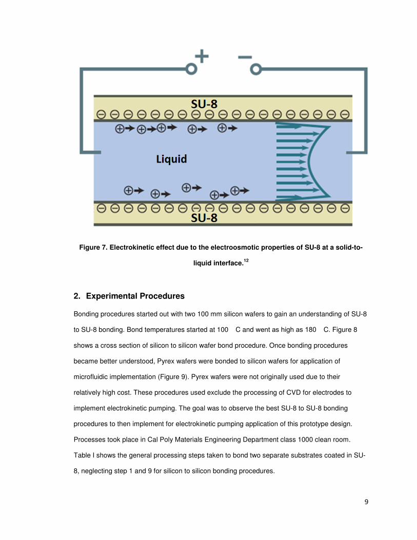
9
Figure 7. Electrokinetic effect due to the electroosmotic properties of SU-8 at a solid-to-
liquid interface.12
2. Experimental Procedures
Bonding procedures started out with two 100 mm silicon wafers to gain an understanding of SU-8
to SU-8 bonding. Bond temperatures started at 100 �C and went as high as 180 �C. Figure 8
shows a cross section of silicon to silicon wafer bond procedure. Once bonding procedures
became better understood, Pyrex wafers were bonded to silicon wafers for application of
microfluidic implementation (Figure 9). Pyrex wafers were not originally used due to their
relatively high cost. These procedures used exclude the processing of CVD for electrodes to
implement electrokinetic pumping. The goal was to observe the best SU-8 to SU-8 bonding
procedures to then implement for electrokinetic pumping application of this prototype design.
Processes took place in Cal Poly Materials Engineering Department class 1000 clean room.
Table I shows the general processing steps taken to bond two separate substrates coated in SU-
8, neglecting step 1 and 9 for silicon to silicon bonding procedures.

10
Figure 8. Preliminary silicon to silicon bond diagram, prior to microfluidic implementation.
Figure 9. Pyrex to silicon bond diagram, after preliminary experiments. Manufactured for
microfluidic implementation.

11
Table I. SU-8 to SU-8 bond processing steps. Step 1 & 9 are neglected for silicon to silicon
bonding procedures.
Step # Processing
1 Mechanical Drilling of Fluid Input/Output
Holes Through Pyrex Wafer
2 Silicon & Pyrex Wafer Clean and
Dehydration
3 Spin Coating of SU-8
4 Soft Bake
5 Exposure and Post Exposure Bake
6 Development
7 Pre-Bond
8 Bond Bake
9 Microfluidic Hookup
2.1. Mechanical Drilling of Fluid Input/Output Holes Through Pyrex Wafer
To prevent later contamination of the wafer, fluid input and output holes were first drilled through
the Pyrex wafer. A 1.5 mm diameter diamond coated drill bit was used to create the holes at spin
speed of 3000 RPMs. Constant drips of water were applied to cool the bit and wash away debris.
Each drilled hole was created with such minimal pressure that contact was only noticeable
audibly. Constant backing out of the bit kept contact area clean and the bit from overheating.
Wafers were securely held with clamps on a rigid plastic backing. These holes were aligned to be
in the same location as the masked region of future photolithography steps. This will eventually
create a complete passage through the wafer for fluid input/output attachments.
2.2. Silicon & Pyrex Wafer Clean and Dehydration
The machined Pyrex wafer and a new silicon wafer are then subjected to a 12 minute basic clean
in Piranha solution. Piranha solution is a mixture of sulfuric acid (H2SO4) and hydrogen peroxide
(H2O2). The basic clean was performed at 70 �C. A five second dip in Buffered Oxide Etch
(BOE), containing hydrofluoric acid, was also performed to remove the native oxide. Extreme
caution was taken during cleaning procedures to avoid skin contact with solution. Chemical
12
gloves, apron, and face mask were used. The wafers are then rinsed and dehydrated at 200 �C
for 30 minutes to evaporate all solvents from the wafer to prevent improper adhesion of SU-8.
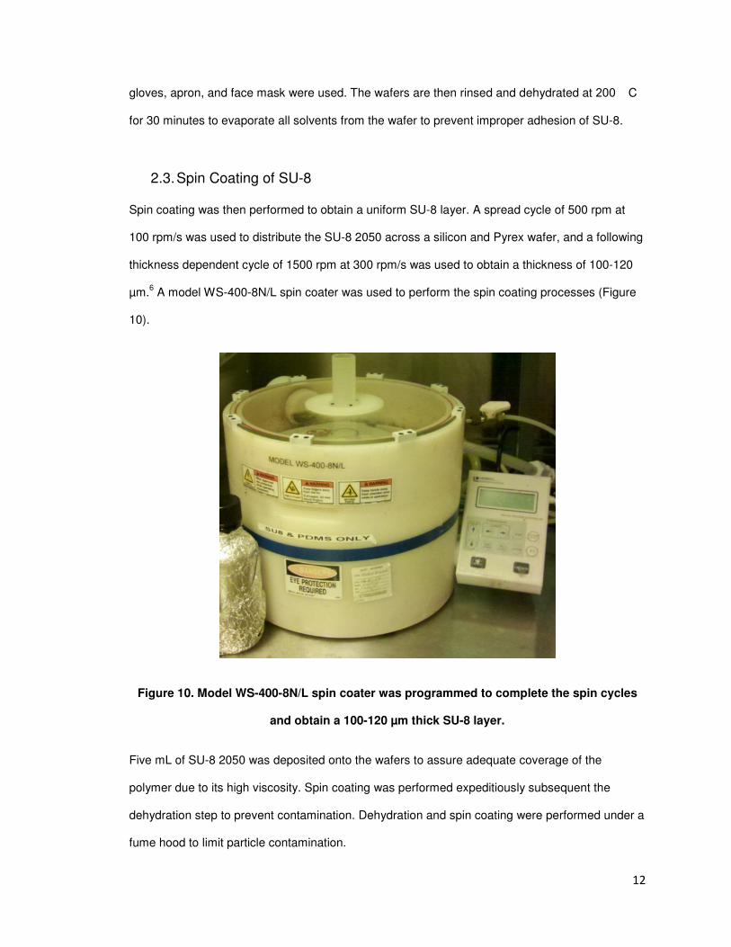
2.3. Spin Coating of SU-8
Spin coating was then performed to obtain a uniform SU-8 layer. A spread cycle of 500 rpm at
100 rpm/s was used to distribute the SU-8 2050 across a silicon and Pyrex wafer, and a following
thickness dependent cycle of 1500 rpm at 300 rpm/s was used to obtain a thickness of 100-120
µm.6 A model WS-400-8N/L spin coater was used to perform the spin coating processes (Figure
10).
Figure 10. Model WS-400-8N/L spin coater was programmed to complete the spin cycles
and obtain a 100-120 µm thick SU-8 layer.
Five mL of SU-8 2050 was deposited onto the wafers to assure adequate coverage of the
polymer due to its high viscosity. Spin coating was performed expeditiously subsequent the
dehydration step to prevent contamination. Dehydration and spin coating were performed under a
fume hood to limit particle contamination.

13
2.4. Soft Bake
After spin coating the wafers were transferred to a hot plate to perform a stepped soft bake. The
step includes a transfer from a hot plate of 65 �C for 5 minutes to a 95 �C hot plate for 15
minutes. The stepping process is used to prevent rapid thermal expansion and thus micro-
cracking within the newly formed SU-8 layer (Figure 11). The soft bake is meant to drive solvents
from the polymer film and to dry the film for subsequent handling. Hot plates were monitored
closely with a thermocouple to ensure temperature stability during the bake (Figure 12).
Figure 11. Micro cracking in an SU-8 layer due to rapid thermal expansion during a wafer
bake step.

14
Figure 12. Hot plates used for dehydration at 200 �C, and step baking at 65 �C and 95 �C
are monitored with a thermocouple. The hot plates are located underneath a fume hood to
prevent contamination during baking procedures.
2.5. Exposure and Post Exposure Bake
After soft baking the wafers and sufficient hardening of the SU-8 layer was observed upon
cooling, photolithography was performed to pattern the SU-8 layers. Photolithography is an
exposure process that is used to remove films of a photosensitive material (Figure 13). SU-8 is a
negative photoresist, so where UV light comes into contact with the photoresist it will start a
chemical process, which, upon a subsequent PEB, makes the polymer insoluble in a liquid
developer. UV light exposure < 350 nm to photosensitive resist results in degraded features,
therefore a long pass filter was used to eliminate these wavelengths. The silicon wafer was
exposed to form microchannels within the SU-8 layer. (During preliminary testing, when two
silicon wafers were used, the second silicon wafer was fully exposed leaving an SU-8 layer
completely covering the wafer).

15
Figure 13. Three major steps of photolithography. First, spin coating to apply the polymer.
Second, exposure to pattern the wafer. Third, development to create exposed features.
The mask used to pattern the silicon wafer can be seen in figure 14. The mask displays where
UV light will hit the SU-8 layer as the light regions, and where the light will be masked from the
SU-8 as the dark regions. The microchannels can be seen as the “T-shape” down the center of
the mask. The additional circular regions that will be developed through the SU-8 layer will
implemented for electrode connection for electrokinetic pumping after SU-8 bond processes are
optimized. The microchannels have been designed to be 200 µm in width. The Pyrex wafer was
patterned with input/output holes for the pump. These holes were aligned with the drilled holes
through the wafer. Upon bonding, these holes were aligned with the “T-shaped” microchannels
and positioned directly above the reservoirs that lie at the end of each channel. The mask for the
Pyrex wafer can be seen in figure 15. A light integral of 35 was used to obtain adequate exposure
through the thick SU-8 layer.

16
Figure 14. Mask used during photolithography of silicon wafer to produce microchannels
within SU-8.

17
Figure 15. Mask used during photolithography of Pyrex wafer to produce input/output
holes through SU-8 layer that are aligned with drilled input/output holes.
Wafers were manually aligned with the masks to avoid degradation of SU-8 layer due to the
machine’s handling mechanisms and lack of ability to recognize the Pyrex wafer. Manual
alignment was also needed on the Pyrex wafer to ensure development of SU-8 directly upon
mechanically drilled holes for future fluid input/output implementation. Manual alignment was
performed by isolating the wafer in between a glass mask blank and the mask (Figure 16).
Spacers were used to keep the mask from contacting the SU-8 layer. A dummy was then used to

18
run through the aligner to initiate the exposure process. A post exposure bake (PEB) was then
performed to further continue the polymer cross linking process of the exposed regions prior to
development. The PEB was also stepped from 65 �C for 3 minutes to 95 �C for 8 minutes to
prevent micro-crack formation. An outline of the mask appeared visible during the PEB and
confirmed adequate exposure of the polymer.
Figure 16. Manual alignment set up to expose SU-8 layer. Spacers were used to keep from
contacting the SU-8. Dummy wafer was sent through the aligner to initiate exposure.
2.6. Development
Wafers were fully submerged upside down in a 3000 mL beaker of developer, polypropylene
glycol methyl ether acetate (PGMEA). They were developed for 14 minutes with occasional
irritation of the developer. Wafers were then individually rinsed with isopropyl alcohol and dried
with a nitrogen gun. If the dried wafers formed a hazy coating, they replaced in the developer for
another minute and then rinsed, dried, and checked again until wafer was clear.
2.7. Pre-Bond
The silicon and Pyrex wafers were simultaneously baked at 85 �C for three minutes to prevent
micro-cracking during the bonding bake. The wafers were then hastily brought together, SU-8 to

19
SU-8. They were then aligned by placing the input/output holes above the fluid reservoirs. While
ensuring alignment, the wafers were then tightened between two plates by a large C-clamp
(Figure 17). The plates were previously heated in the bond bake oven to the bond temperature.
Figure 17. Wafer clamping setup. Wafers are clamped in between the top and bottom plate.
Plates previously heated to bond temperature.
2.8. Bond Bake
Bonding was carried out at multiple different temperatures for 20 minutes. To gain an
understanding of SU-8 to SU-8 bonding, two reused silicon wafers were used in the processing
procedures in order to save money. Bond temperatures of 100 �C, 120 �C, 140 �C, 150 �C,
160 �C, 170 �C, and 180 �C were performed to conceive the best parameters for bonding. A
small oven was used to perform bake (Figure 18). Once bonding procedures were better
understood, a Pyrex wafer was used to bond to the patterned silicon wafer. With Pyrex wafer

20
implementation, bond temperatures of 160 �C and 170 �C were used at bond times of 20
minutes.
Figure 18. Bond bake furnace that would contain entire bond apparatus. Temperature was
monitored by a thermocouple.
2.9. PDMS Microfluidic Hookup
Polydimethylsiloxane (PDMS) was cured and cut into small squares for microfluidic hookup.
Syringe needles were pressed through the PDMS to create a squeeze fit to prevent leakage. The
needle tip was positioned so that it was just beneath the PDMS surface, so that it would not
interrupt the PDMS to Pyrex bond. The PDMS was then bonded to the glass wafer using argon
plasma. The syringe tip was positioned directly above the drilled input/output holes to create a
passage from the syringe, through the needle, and into the microfluidic channels. Figure 19
shows a picture of a complete silicon to Pyrex microfluidic chip with PDMS input and output
hookups.

21
Figure 19. Complete silicon to Pyrex microfluidic chip with PDMS fluid hookups.
3. Results & Discussion of Bonding Processes
3.1. Silicon to Silicon Wafer Bonding
The goal of bonding two reused silicon wafers was to determine the bond temperature that would
yield the strongest bond. The results that were investigated remained whether the SU-8 withheld
the integrity of the features produced during photolithography, as well as the strongest bond
strength. Bond strength was measured by prying the silicon wafers apart with wafer tweezers and
subsequently the SU-8 features were investigated. This bond strength test method is known as
the “open-crack method” and only gives a rough estimate of the bond strength.13
Table II shows
the results of silicon to silicon bond strengths. Bond temperatures started at 100 �C and found

22
poor bond quality, yet signs of polymer cross linking across the two substrates. Bond temperature
of 120 �C improved in bond quality and strength. Slightly noticeable increases in bond strength
continued up through bond bake temperatures of 170 �C. Wafers were broken apart with
tweezers and noticeable signs of channel bonding occurred. Out of the two silicon wafers with an
SU-8 layer, one that had been patterned with photolithography and one that had not, the wafer
that had not been patterned showed features of channels and reservoirs that had been
transferred from the patterned wafer (Figure 20, 21).
Table II. Results of Silicon to Silicon wafer bond quality and SU-8

23
Figure 20. Signs of bonding around the reservoir in SU-8 after bond was broken apart.
Note: Silicon wafer in image was not patterned with photolithography.
Figure 21. Signs of bonding around the channels in SU-8 after bond was broken apart.
Note: Silicon wafer in image was not patterned with photolithography.

24
In addition, channel integrity was withheld up until a bond temperature of 180 �C was
implemented. A JEOL scanning electron microscope (SEM) was used to assure that the SU-8
structure of the channel walls were not degrading. It was found that around bond temperatures of
180 �C, the glass transition temperature was reached and the channel walls started to degrade
and flow out of the wafer bond apparatus due to the applied mechanical pressure. Figure 22 & 23
shows SEM images of channels at bond temperature 170 �C.
Figure 22. Cross section SEM image (30x magnification) of SU-8 microchannels and
reservoir. Image shows channel integrity withheld at bond temperature 170 �C.

25
Figure 23. SEM high magnification cross section image of microchannels. Image shows
channel integrity withheld at bond temperature 170 �C.
Once an understanding was gained during silicon to silicon wafer bonding, Pyrex wafers were
used in processing. This was done in order to save money.
3.2. Silicon to Pyrex Wafer Bonding
Pyrex wafers were implemented in the processing procedures for the purpose of drilling through
the amorphous wafer for microfluidic input/output hookups. Pyrex is also used for its property of
optical transparency for the purpose of making empirical observations of lab testing. Same
processing procedures were used with the inclusion of step 1 and 9 (Table I); drilling through the
Pyrex wafers and microfluidic input and output hookup through PDMS bonding. Bonding
temperatures of 160 �C and 170 �C were used in SU-8 to SU-8 bonding procedures with Pyrex
wafers, as these were seen as the strongest bonds that withheld channel integrity. When fluid
was mechanically pumped via syringe into the channels, the fluid quickly jumped the microfluidic

26
channel boundary and rapidly dispersed throughout the entire wafer. Upon this result, wafers
were sectioned and different bond areas were investigated. Figure 24 shows an example of
different bond areas that were investigated.
Figure 24. Complete silicon to Pyrex microfluidic chip by SU-8 to SU-8 bonding. Red
circles indicate fully bonded areas. Blue circles indicate partially bonded areas. Bond
temperature 160 �C.
The dark areas marked by red circles of figure 24 represent fully bonded regions of SU-8 to SU-8.
The lighter areas that are marked by blue circles of figure 24 represent areas of partially bonded
SU-8 to SU-8. This conclusion was drawn by sectioning the wafers and polishing their cross
sections. Figure 25 represents the dark region marked by the red circle in figure 24.
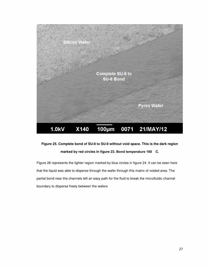
27
Figure 25. Complete bond of SU-8 to SU-8 without void space. This is the dark region
marked by red circles in figure 23. Bond temperature 160 �C.
Figure 26 represents the lighter region marked by blue circles in figure 24. It can be seen here
that the liquid was able to disperse through the wafer through this matrix of voided area. The
partial bond near the channels left an easy path for the fluid to break the microfluidic channel
boundary to disperse freely between the wafers

28
Figure 26. Partially bonded SU-8 to SU-8 with void space allowing for fluid passageways.
This is the light region marked by blue circles in figure 23. Bond temperature 160 �C.
With these results it was found that parts of the wafer began to bond, where other parts had a
matrix of partially bonded regions that create voids. These voids lead to easy fluid passageways
that allow fluid movement throughout the wafer. Microfluidic implementation is impossible while
this problem exists. Changing of bonding procedures must be made to eliminate void area at the
bond interface.

29
4. Conclusions and Continuation of Project
4.1. Changes to Procedures
Results show that there is incomplete SU-8 to SU-8 bonding. Voids are present in the bond which
is letting the fluid easily disperse between the wafers. Upon process changes for the project,
several methods will be tested to obtain a more complete bond. The first method will be
implementing the bonding procedure in a vacuum furnace. Undergoing bonding procedures under
vacuum should pull the wafers together and evacuate the molecules from between the
substrates. This will eliminate gasses and solvents that create voids between the SU-8 layers.
The second method will be to lengthen bonding times. A bonding time of 20 minutes is relatively
short. Longer times may initiate further bonding of the SU-8 layers if further cross linking is still
possible. The third method will be to apply a greater external pressure against the wafers in
addition to the vacuum. The pressure should cause stress in the polymer layer which should
result in movement of the polymer chains. The heated polymer chains should flow together and
form strong covalent or ionic bonds across the SU-8 to SU-8 gap to relieve stress. The clamping
plates will be grated to allow for gas escape through the drilled input and output holes in addition
to the sides of the wafer. This should allow for a more complete bond across the substrates and a
fully sealed microfluidic chip. Once the SU-8 to SU-8 bond procedures are finalized, mechanical
pressure testing of bond strength will be analyzed by a fluid burst test. In this test fluid will be
mechanically pumped through the channels and pumping pressures will be measured until failure.
This will give a good idea of the SU-8 to SU-8 bond strength for microfluidic applications.
4.2. Continuation of Project
Further continuation of the project will include implementation of processing procedures to
deposit metal contact electrodes for electrokinetic pumping implementation. Procedures will be
optimized for electrokinetic pumping to allow for a complete absence of mechanical actuation.
The electroosmotic properties of the SU-8 to liquid interface interacting with the electric field
30
produced, will obtain volumetric fluid velocities which will be analyzed for a microfluidic drug
dispensing device. Recent studies have observed that SU-8 displays an electroosmotic mobility
of 4.5E-4 ��
� with buffer solutions of ~7 pH.
2 With an applied voltage difference of 200 V and
channels that are ~6 cm long; this gives an estimated fluid velocity of 0.015 �� �⁄ . This is
calculated for channels that are more than twice the diameter of the channels discussed in this
report. With smaller channel diameter, this pumping velocity would increase. Low pumping
velocities also mean precise amounts of fluid can be pumped, which could be beneficial to this
design.

31
References
[1] Merriam-Webster.com. Merriam-Webster, 2012. Web. 29 May 2012.
[2] Sikanen. "Characterization of SU-8 for Electrokinetic Microfluidic Applications." Lab on a
Chip 5.8 (2005): 888. Print.
[3] "Clinical:Novolog (insulin Aspart)." - Medpedia. Web. 09 Apr. 2012.
<http://wiki.medpedia.com/Clinical:Novolog_(insulin_aspart)>.
[4] "SAFE SYRINGE DISPOSAL GUIDE FOR HOME GENERATED MEDICAL WASTE." New
Jersey Department of Health and Senior Services. Web. 4 Apr. 2012.
<http://www.state.nj.us/health/eoh/phss/syringe.pdf>.
[5] Whitesides, George M. "The Origins and the Future of Microfluidics." Nature 422
(2006).Nature.com. 27 July 2006. Web. 19 Mar. 2012.
<http://students.sabanciuniv.edu/~tabak/references/pdf/Whitesides_2006.pdf>.
[5] “NIHERST: Make Way for Fluidics!" The National Institute of Higher Education, Research,
Science and Technology. Web. 19 Apr. 2012. <http://www.niherst.gov.tt/scipop/sci-
bits/microfluidics.htm>.
[6] "SU-8 2000: Permanent Epoxy Negative Photoresist." MicroChem. Web. 26 Apr. 2012.
<www.microchem.com>.
[7] "Low Reynolds Number Flows." Hitech-Projects. Web. 30 May 2012. <http://www.hitech-
projects.com/euprojects/artic/index/Low%20Reynolds%20number%20flows.pdf>.
[8] Altpeter, D. M. "Description of SU-8." (4/13/2005).
[9] Bhushan, Bharat. "Biomimetics Inspired Surfaces for Drag Reduction and
Oleophobicity/philicity." Beilstein J. Nanotechnol (2011): 66-84. Print.
[10] Wong, Pak Kin. "Electrokinetics in Micro Devices for Biotechnology
Applications."IEEE/ASME TRANSACTIONS ON MECHATRONICS 9.2 (2004). Web. 30
Apr. 2012. <http://www.me.jhu.edu/thwang/publications/Mechatronics9(2)366.pdf>.
[11] Santiago, Juan. "Stanford University." Electrokinetic Bioanalytical Systems. Web. 30 Apr.
2012. <http://microfluidics.stanford.edu/Projects/Archive/bioanal.htm>.
[12] "ALChemE." Electrokinetics. Web. 29 May 2012.
<http://alcheme.tamu.edu/?page_id=6823>.

32
[13] Blanco, F. J., M. Agirregabiria, J. Garcia, J. Berganzo, M. Tijero, M. T. Arroyo, J. M. Ruano,
I. Aramburu, and Kepa Mayora. "Novel Three-dimensional Embedded SU-8
Microchannels Fabricated Using a Low Temperature Full Wafer Adhesive
Bonding."Journal of Micromechanics and Microengineering 14.7 (2004): 1047-056. Print.