boron-doped diamond growth...
TRANSCRIPT
1
MCN FIRST IN AUSTRALIA TO HAVE BORON-DOPED DIAMOND GROWTH CAPABILITY
Diamond Deposition SystemsSPIE Conference Be rewarded for your workFIBSEM enhanced by gripper
Thinner electronics on horizonIndustry meets research at COMSPrestigious journal coupsCrowd funding the new frontierNanopatch vaccinationsNew PVD Sputter System
1233
444556
IN THIS EDITION
OCTOBER 2013
MCN will become the first facility in Australia to be able to grow both ultra-high-purity, as well as boron-doped diamond, both of which are useful in the creation of semi conducting materials. This is possible with the installation of two state-of -the-art, chemical vapour deposition (CVD) diamond systems.
A notoriously unstable and unyeilding material, diamond has previously been successfully grown through high pressure, high temperature systems which heat carbon to around 2500 degrees Celsius and apply pressure equivalent to the weight of the Eiffel Tower applied through its tip. These presses are large, expensive and difficult to run and cannot easily achieve a pure diamond outcome.
CVD systems, however, use a continuous microwave source to heat hydrogen and carbon (in the form of methane) to between 700 and 1000 degrees Celsius. This breaks down the atoms to become a highly reactive plasma. When the plasma hits an existing diamond sample surface, the hydrogen stabilises the diamond structure, while the methane adds carbon in diamond lattices to the existing material. The systems are able to fabricate either single crystal layers or polycrystalline growths.
Across the world, diamond’s biggest use is in cutting and grinding with 70% of mined diamonds sold for industrial applications, while its second biggest use is in the gem stone industry.1 However, it is also of interest to a number of different sectors within the scientific community as it is the hardest naturally occurring material, is an effective heat conductor, expands very little in high temperatures and is resistant to most acids and alkalis.
Dr Alastair Stacey, a materials scientist at Bionic Vision Australia, says there is a growing diamond community in the Australian research industry. “Diamond is useful for all sorts of applications such as quantum information processing, electronics and medical bionics,” Dr Stacey said. “We are using it in the Bionic eye project to make
bionic compatible devices.” Diamond is an ideal material for this, as bionic devices need to be both safe for the human body and suitable for being implanted. Some materials which are biocompatible are rejected or attacked by the body, whereas diamond is unique in that it is both bio-safe and accepted. It is also an unyielding material which is unlikely to break, as well as being hermetic, which makes it ideal for encasing electronics and protecting them against fluids. Lastly, when doped with boron it can conduct energy, predisposing it to use in electronics.
Bionic Vision Australia (BVA) through the Melbourne Materials Institute has been using the two diamond deposition systems currently in place at the University of Melbourne, which is one of its five core members. However, with the installation of the two new systems at MCN, which have been partially funded by BVA, a higher quality of diamond can now be achieved, as well as boron-doped semiconducting diamond. “This is an exciting direction for the research community,” Dr Stacey said. “We expect to see a lot of growth in this area.” The systems will be available for use by the end of November 2013. For more information or user inquiries, please email [email protected]
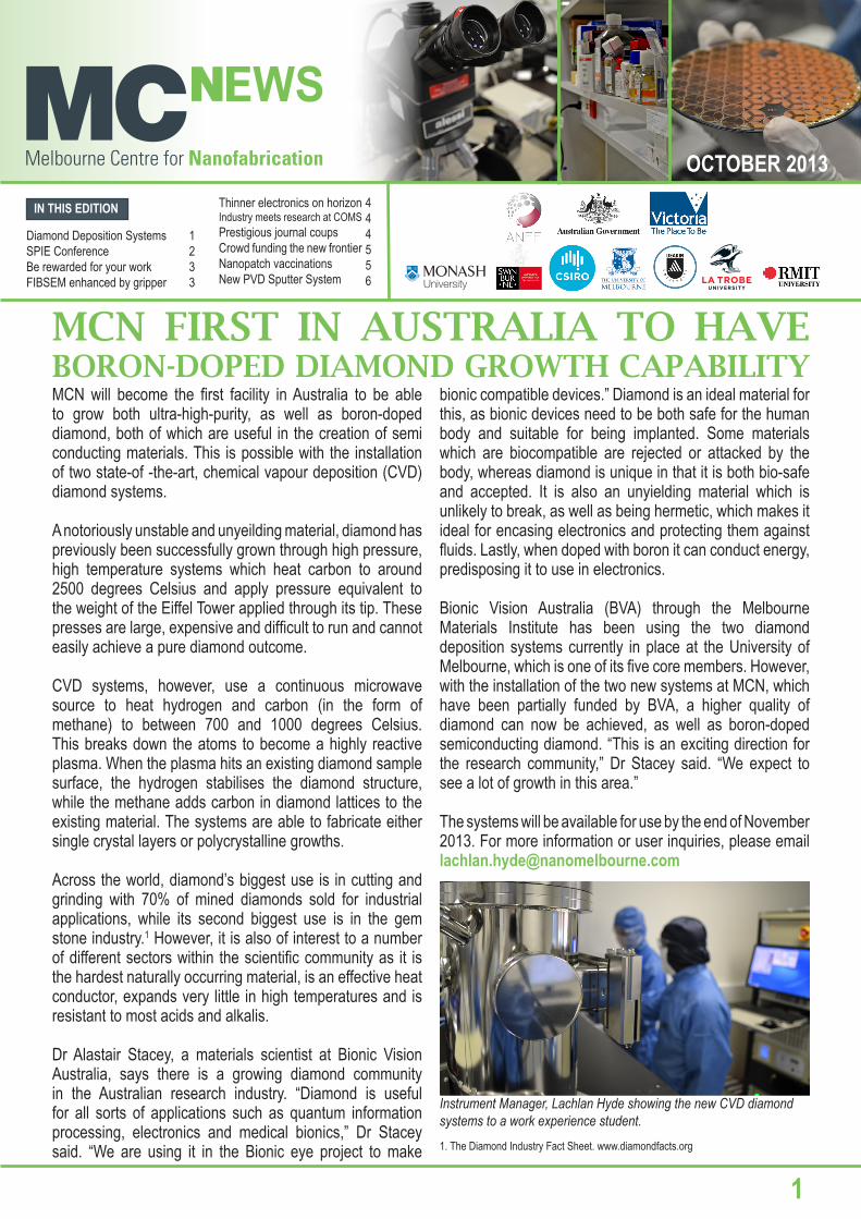
Instrument Manager, Lachlan Hyde showing the new CVD diamond systems to a work experience student. 1. The Diamond Industry Fact Sheet. www.diamondfacts.org

2
MCN is proud to partner with ANFF as sponsors for the SPIE Micro+Nano Materials, Devices, and Applications Conference, to be held from Sunday 8 December to Wednesday 11 December this year at RMIT in Melbourne.
Last held in 2011, the conference is a four-day summit, bringing in experts from around the world to discuss topics such as nanofluidics, plasmonics, solar energies, MEMS, phototonics and much more.
MCN projects feature heavily on the schedule with 27 out of the 210 papers and posters being presented at the conference, co-authored by MCN staff or Tech Fellows. These highlight the valuable work undertaken at MCN. See
below for a list of these publications as well as an overview of the three plenary speakers.
Yet another drawcard for the conference is that fabrication equipment and technology companies, such as Warsash, Realtek, Coltronics and Grey Innovation will be exhibiting new products and presenting on their innovations.
The SPIE Micro+Nano Materials, Devices and Applications Conference is unmissable for those interested or working in fabrication innovations and technologies. Register at http://spie.org/x27145.xml before 21 November 2013 to secure early bird rates.
SPIE CONFERENCE BRINGS TOGETHER NANO EXPERTS
PLENARY 3HYDRODYNAMIC CHALLENGES IN INKJET PRINTING Dr. Detlef LohseUniversity of Twente
Expert in micro and nano fluidics, Dr Detlef Lohse will be discussing the various scientific challenges to optimised high performance printing such as droplet formation and droplet impact on substrates, as well as the coupling between fluid dynamics and acoustics.
PLENARY 1SEMICONDUCTOR NANOSTRUCTURES IN ENERGY DEVICES Prof. Daniel DapkusUniversity of Southern California Leading researcher in the field of energy nano-science, Professor Daniel Dapkus has been researching how to create highly efficient solar cells and LEDs utilising semiconductor nanorods to form the cell components. He will discuss prospects for droop-free LEDs and multijunction solar cells.
PLENARY 2NANOPHOTONICS FOR BIOLOGYProf. Tanya MonroUniversity of Adelaide
An ARC Federation Fellow and Director of the Institute for Photonics and Advanced Sensing, Professor Tanya Monro will be highlighting new advances in the development of optical materials, structures and sensors as well as fluorescent sensing architectures that are more powerful than ever before.
MCN CO-AUTHORED PAPERS & POSTERS TO BE PRESENTED AT SPIE 2013• Micro-optical system-on-a-chip• Asymmetric cross-shaped slot antennas surrounded
with periodic corrugations• Rapid formation of controlled size and morphology
spheroids by surface acoustic wave microfluidic device (SAW) versus liquid overlay method,
• Vanadium dioxide thickness effects on tunable optical antennas
• Micro pore arrays in free standing cyclicolefincopolymer membranes: fabrication and surface functionalization strategies for in-vitro barrier tissue models
• Acoustowetting: film spreading, fingering instabilities and soliton-like wave propagation
• Mapping the effect of pulsed surface acoustic waves on a sessile drop
• Characterization of magnetic force driven microflow• Surface acoustic wave (SAW) atomization of
therapeutic antibodies for pulmonary delivery
• Gen silencing using siRNA• Measuring nanobubble properties using a novel
method• Flow through a microfluidic chip induced by a distal
surface acoustic wave atomizing suction pump• Surface acoustic waves-assisted technique for
generation of individual carbon nanotubes and their shear-induced alignment
• Investigation of periodically poled 128˚ YXcut LiNbO3 achieved with UV direct-written technique for SAW generation
• SAW generation in acoustic superlattice lithium niobate: methods of converting bound acoustic resonances to propagating waves
• Three-dimensional cell patterning in hydrogel by ultrasound standing waves
• Black-Si as a platform for sensing• Evaluation of optical fibres for surface enhanced
Raman scattering probes
• Laser nanostructured surface for biomedical sensing using surface-enhanced Raman spectroscopic mapping
• Hybridization in 3D: optical and plasmonic elements• THz photomixer with a sub-50 nm nanoelectrode gap
on low temperature grown GaAs• Ion-beam and plasma etching of a conicalpores
photonic crystal for thin-film solar cell• Fabrication and replication of micro-optical structures
for growth of GaN-based light emitting diode• Optical and thermal characterization on micro-optical
elements made by femtosecond laser writing• Characterization of optical polarization converters
made by femtosecond laser writing• How to fabricate robust microfluidic systems for a
dollar• Integrated microdroplet-based system for enzyme
synthesis and sampling

3
Et voluptas adias dolent molum qui diciend ianimus.On erro dolorei ciaspie nimpores voluptatur as simust a venis volo intecte nihiliandae. Volorupta conectorrunt odis et ut vollent, comnim litis incti reritius doluptate es eosam quid qui doluptam quasper chitatem in consenecto ium fugia am res ex estio. Fer-natur alit quid quas et aute veles min esto beatumOn et, im nis dolorioria nos alibusc ipsamus poribusaes nis molesci tionseres molorrum etur antur?Undusap erferem. Ullupta etur ad quos esti quo maxim etur au-digenditi que nimiliq uianti bla nonsequis audae non nobitaquae laccabo. Nam, te nescipit et quamenis essundis
alitam, optur sedia ideleca borero beatur, simus velendia nonsequam rehenimagnis sequis endigenia conseritat qui dem. Nempore sus et re aute moditae as con rem. Nam que dolor modit labore, optas aut ut esed ulla dolore voluptasped magnat et, qui a quatae odiantur re esecturero ommolla borendae odit, esed et est, consequ issumquianto ent aut officip itatecu scienti usamus, imi, que sunt reria inum quam, odis mossitatia il magnitae quamust, sequat et que nis et ressusant.Maximaio. Itatae ea in porpor sus volliquam, officim ad quatqui que pa dolupta non pa iligniat molupta tetur?Lorersperum eribus consend esequassus dis sum verrum lab-orepelit volupta spitin nam fugitatemod quat.
Caborrovidus eate mil eaquatu rionsequiat.Net ut hariore same ommodiciet estia aut volecabo. Et eaquae corecus is modicid magnimagnis aut mo coriam laborepres debis asperci asperuptatum nisquatem quam, quasperum volupta tinctur?Faccae con porestiatem. Ut et modi veliquo tem. Ut mil il millabo rerorpo reius.On pro ipsapicae numquas quunt ulparum dist explign imil-luptaque nonet quatur? Quiat facepedita doluptae sum, que consecus molupis doluptaturis dolor aut evenda nest assimus
SHOW YOUR POSTER AT SPIE FOR A CHANCE TO WIN!ANFF is offering its staff and users the opportunity to win a share of $500 with a $250 award for both Best Poster and Best Image.
The posters should highlight a valuable or novel fabrication process and should reference how ANFF has faciliated this work.
The posters will be displayed during a specific ANFF poster workshop at the SPIE conference on Tuesday 10 December 2013 from 3:30-5:30PM and the winners announced at the SPIE Gala Dinner on Tuesday evening from 6:30PM.
Please submit your posters to [email protected] by November 1 2013, with a 150 word abstract, the poster’s title, author and a list of affilitations and make sure you are registered for the day at the SPIE conference to be eligible for the competition.
NOVEL PROCESS POSTER
MCN’S image of the year competition is back on and open to all MCN users. Users are invited to submit any images, photographic or scientific, of work undertaken at MCN for the chance to win a $200 voucher to a restaurant of their choosing. For all the details and information on how to enter, visit http://nanomelbourne.com/image-competition. Entries close at 5pm on November 8 and the winner will be notified within two weeks.
IMAGE OF THE YEAR COMP!
BE REWARDED FOR YOUR WORK
FIB-SEM ENHANCED WITH MICRO GRIPPER MCN’s Dual Beam FIB-SEM has been enhanced with the Kleindiek Nanotechnik Lift-Out Shuttle which features a three axis sub stage and high resolution micro gripper for transport and assembly of micro sized objects. It allows efficient sample preparation for TEM as well as atom probe microscopy. The gripper ensures that the FIB cut sample is held securely and non destructively, eliminating the need for time consuming ion beam induced deposition and ion beam cutting steps associated with using a single probe tip micro manipulator. This ultimately allows for reduced cost, higher throughput sample preparation with higher yield in a shorter time frame than previously possible.
To add further value to the FEI Helios Nanolab 600 FIB-SEM, additional upgrades and accessories will be deployed over the next few months. These include a Quick Loader chamber which allows sample exchanges 30 times faster than currently possible; Nanobuilder software which is used to automatically fabricate complex multilayer nanostructures, offering high precision ion beam control including automated beam alignment and drift control; as well as a Metal-enhanced Etch Gas Injection System which will enhance the FIB etch rate and shorten the milling time of large areas on silicon and metallic substrates. For more information on the micro-gripper or any of the planned upgrades, please contact [email protected]

4
Imagine a TV screen you could roll up and take on holiday with you or a paper-thin digital watch that wraps around your wrist in a transparent shimmer. ARC Laureate Fellow Michael Fuhrer and his team from the school of physics at Monash University, are helping to make these futuristic technologies a realistic possibility.
“The work we’re doing is leading towards smaller, thinner, more robust electronics technologies,” said Jacob Tosado, a member of the Fuhrer research team. The group is investigating atomically-thin two-dimensional materials such as graphene (a single atom-thick plane of graphite), and layered transition-metal dichalcogenides such as molybdenum disulphide. These single layer materials can be practically transparent and can have extraordinary properties. For example, graphene is stronger than steel and can be more conducting than copper, while molybdenum disulphide is a semiconductor that can be used to make working transistors which are just a few atoms thick. These new materials could lead to new types of flexible, transparent electronic devices.
Single layer crystals are isolated at Monash University’s School of Physics, after which they are brought to the MCN for further analysis. The group
uses MCN’s Atomic Force Microscope capabilities to assess the quality of their samples. The Nikon Eclipse Ti Confocal Microscope and the CytoViva Hyperspectral Microscope allow them to further characterise the crystals’ photo luminescent properties. The group is currently investigating the optical and electron-beam lithography capabilities at MCN for fabricating electronic devices from these 2-D materials.
“MCN demonstrates the capability to characterise low dimensional, semi-conducting materials,” Tosado explained. Within six months of coming from the University of Maryland, the Fuhrer group has been able to recommence their research in fundamental physics by using the resources of the MCN.
THINNER, MORE DURABLE ELECTRONICS ON THE HORIZON
Victorian research organisations had a strong presence at this year’s COMS (Commercialization of Micro and Nano Systems) conference, held in the Netherlands in August.
COMS is the only conference world-wide to be dedicated to the commercialisation process for micro and nanofabrication technologies. Bringing together leaders in nanofabrication from across the globe, COMS creates productive partnerships and focuses on entrepreneurship and marketable nano solutions.
Plenary sessions included how to connect market needs with emerging technologies, and how to cross academic, industry and government boundaries to create a fruitful innovation environment that fulfils research goals and achieves marketable products.
“The conference was particularly valuable for its unique convergence of large scale nanofabrication research labs with an active and focused investment community, all within the specialised precinct of Kennispark,” said MCN’s Managing Director, Dwayne Kirk.
INDUSTRY MEETS RESEARCH AT
COMS 2013
MCN’s Managing Director, Dwayne Kirk, with Ron Lawes and Clive Davenport from Small Technologies Cluster, Bruce Whan from Swinburne University and Lily Chisholm from Monash University.
Two recent publications penned by MCN staff, users and Tech Fellows have been highlighted in prestigious journal, Nature Materials. “The Dark Side of Plasmonics,” co-authored by MCN Tech Fellows Dr Daniel Gomez and Dr Tim Davis of CSIRO and MCN Senior Process Engineer Matteo Altissimo has been highlighted, as has “Combining UV Lithography and an Imprinting Techniquefor Patterning Metal-Organic Frameworks,” by Doherty et al. A big congratulations goes to all involved in the publications. Details of the articles can be found here:http://www.nature.com/nmat/journal/v12/n10/full/nmat3770.htmlhttp://www.nature.com/nmat/journal/v12/n9/full/nmat3752.html
PRESTIGIOUS JOURNAL COUPS FOR MCN USERS AND TECH FELLOWS
Gold electrodes contacting single layer graphene. The patterns are written using the IMP direct write lithography system. Image taken by Changxi Zheng, a member of the Fuhrer research group.

5
NANOPATCH TAKING THE HURT OUT OF VACCINES
Vaccinations, though vital in preventing the spread of disease in the modern world, have several major drawbacks which limit their effectiveness and uptake in developing countries.
Professor Mark Kendall from the Australian Institute of Bioengineering and Nanotechnology, has spent the last ten years developing the Nanopatch - a needle free solution to many of the problems facing vaccine use. A tiny square of microneedles coated in vaccine, the Nanopatch is simply placed on the skin and the vaccine dispersed into the immune system just below the skin.
Vaxxas Pty Ltd, which was established to develop the Nanopatch, engaged with MCN at the beginning of the year to increase the outputs of their trial patches. By providing Vaxxas with access to state-of-the-art development equipment and expertise, MCN has accelerated and improved the production of the Nanopatch.
Eliminating the pain of traditional injections is just one small advantage of the Nanopatch. As the vaccine is dry coated onto the patch, the need for refrigeration is eliminated. This vastly increases its stability and reduces cost barriers for transporting vaccines to where they are needed most in third world countries. Similarly, the need for highly-trained professionals
to administer the medications is diminished. In this way, the Nanopatch has the capacity to transform the world’s disease landscape, and to stamp out illnesses in third world countries that have long been preventable in the developed world. Furthermore, because the vaccine is delivered straight into the immunological cells, preclinical trials have shown a strong immune response with much lower doses than conventional intramuscular injections.
The Nanopatch is manufactured using mono-crystalline silicon wafers which are subjected to deep-reactive ion etching (DRIE), the same proccess that is commonly used to fabricate components of smart phones and other microtechnology devices.
Over the last ten months, MCN has helped to fine tune the Nanopatch production process so that the layers deposited on these wafers achieves better uniformity, increasing the output from each wafer. Furthermore, MCN has allowed Vaxxas to move from 4 inch wafers to 6 inch wafers, once again increasing the yield. MCN also hosts two DRIE systems which enables them to double their final outputs by processing wafers in parallel.
More information on the Nanopatch can be found at www.vaxxas.com
CROWD SOURCING THE NEW FRONTIERHave a great idea for a research project but not quite sure how to fund it? Government funding is available through ARC and NHMRC grants, though these are often highly competitive forums for funding.
Crowd sourcing, which has been popular since 2009 in the creative industries in particular, has begun to make a name for itself in research communities too.
Sites such as Kickstarter, and Pozible connect entrepreneurs with people interested in seeing a new idea succeed. Supporters can donate anywhere between $2 and several thousand dollars to help entrepreneurs get their project off the ground. In some cases, investors are rewarded with a share in the project should the item succeed and in other cases, people get involved just to support an idea that they think worthwhile.
Now sites such as Microryza and Petridish, are looking to give science research projects a voice in the crowd funding sphere.
Successful crowd funding projects build a narrative around the concept and keep supporters informed of developments through social media, keeping the community discussion alive. Not only is crowd-funding an alternative way to fund your research project, it is an amazing way of connecting to the community and voicing the importance of your scientific endeavours.
For more info head to: www.microryza.com or www.petridish.org

6
NEW FACES AT MCN Sarah Abramson (Communications Coordinator)
Melbourne Centre for Nanofabrication03 9902 4073 | 151 Wellington Rd Clayton 3168 | [email protected] | www.nanomelbourne.com | www.anff.orgDr Dwayne Kirk - MCN Managing Director | [email protected] | 03 9902 4049Dr Gareth Moorhead - MCN Science Director | [email protected] | 03 9902 4073
MCN presents at NanoS-E3
MCN’s Dr Matteo Altissimo recently participated in the fourth NanoS-E3 Conference in Queensland. The workshop brought together Nanotechnology experts with a focus on sensors, electronics, energy and the environment.
Recognising these four fields as critical in the growth of nanotechnologies and their applications in the world economy, the NanoS-E3 workshops aimsto foster collaboration between Nanoscience researchers who are currently undertaking work that has the possibility to transform a range of scientific endeavours.
Speaking about Electron Beam Lithography research undertaken at MCN, Matteo discussed high level work in the fields of plasmonics and nano-sensing, performed by Dr Xingzhan Wei and Thanh Nguyen from the University of Melbourne and Dr Daniel Gomez from CSIRO. The works were selected because they highlight the outstanding capabilities of the MCN’s Electron Beam Lithography tool.
About the conference, Dr Altissimo said, “It was a fantastic opportunity to network with colleagues and friends from Australia and overseas, as well as a perfect chance to present MCN’s capabilities to a new audience, some of who had not previously heard about the centre.”
Sarah is responsible for MCN’s written communications, website content and visual branding. Graduating from the University of Melbourne with a bachelor in Media and Communications in 2009, Sarah has been working in marketing and communications in both academic and commercial settings. She brings with her experience in video creation, copywriting and graphic design. Please contact [email protected] with any communications or media inquiries.
NEW PVD SPUTTER SYSTEM ONLINE Adding to MCN’s already expansive thin film deposition capabilities, we are now pleased to house an ANATECH Hummer RF/DC Sputter System.
The new sputter deposition system is a physical vapour deposition sputter system and can not only deposit metals, but also oxides and nitrides with high precision. This unique capability will allow users to directly deposit insulating layers onto their thin films, saving time and achieving more precise layers.
The Hummer sputter system is now fully operational and we expect it to be in high demand among MCN users. For more information, please contact [email protected]
Above: The Hummer RF/DC Sputter System.
MCN inductions will now be held on the first and third Monday of the month only. Inductions are compulsory for all users of the centre and refresher courses are required every year. The times for inductions are as follows:
For more information contact [email protected].
10AM-12:30PM MCN general induction 1PM-2:15PM Dangerous Goods Waste Management3PM Local Area Induction
INDUCTIONS NOW BIMONTHLY
Left: The Hummer BC-20’s round planar chamber with three 3-inch round sources.