bq25122 low iq highly integrated battery charge management
TRANSCRIPT

BQ25122 Low IQ Highly Integrated Battery Charge Management Solution for Hearables, Wearables, and IoT
1 Features• Increases system operation time between charges
– Configurable 300-mA buck regulator(1.2-V default)
– 700-nA (typical) Iq with buck converter enabled (no load)
– Configurable load switch or 100-mA LDO output (load switch enabled by default)
– Up to 300-mA charge current for fast charging– 0.5% Accurate battery voltage regulation
(configurable from 3.6 V to 4.65 V in 10-mV steps)
– Configurable termination current down to500 µA
– Simple voltage based battery monitor• Highly integrated solution with small footprint
– 2.5 mm x 2.5 mm WCSP package and 6 external components for minimal solution
– Push-button wake-up and reset with adjustable timers
– Power Path management for powering the system and charging the battery
– Power Path management enables < 50 nA 150-nA Ship Mode battery quiescent current for longest shelf life
– Battery charger operates from 3.4 V – 5.5 VIN (5.5-V OVP / 20-V tolerant)
– Dedicated pins for input current limit, charge current, termination current, and status output
• I2C Communication control– Charge voltage and current– Termination threshold– Input current limit– Load switch control– Controls for interrupts for faults and status– System output voltage adjustment– LDO Output voltage adjustment
• Safety-Related Certification:– TUV IEC 62368-1 Certification
2 Applications• Hearing aids, hearables, smart watches, and other
wearable devices• Fitness accessories• Health monitoring medical accessories• Rechargeable toys
3 DescriptionThe BQ25122 is a highly integrated battery charge management IC that integrates the most common functions for wearable devices: Linear charger, regulated output, load switch, manual reset with timer, and battery voltage monitor. The integrated buck converter is a high efficiency, low IQ switcher using DCS control that extends light load efficiency down to 10-µA load currents. The low quiescent current during operation and shutdown enables maximum battery life. The device supports charge currents from 5 mA to 300 mA.
Device InformationPART NUMBER PACKAGE(1) BODY SIZE (NOM)
BQ25122 DSBGA (25) 2.50 mm x 2.50 mm
(1) For all available packages, see the orderable addendum at the end of the data sheet.
GND
HOST SDA
SCL
INT
SW
BAT
MR
BQ25122
MCU / SYSTEM
-+
NTCTS
LS / LDO
<100mALoad
IN
SYS
RESET
LSCTRL
VINLS
Unregulated
Load
PMIDPG
IPRETERM
ISET
ILIM
CD
IN
Simplified Schematic
BQ25122SLUSD33A – NOVEMBER 2017 – REVISED JANUARY 2021
An IMPORTANT NOTICE at the end of this data sheet addresses availability, warranty, changes, use in safety-critical applications, intellectual property matters and other important disclaimers. PRODUCTION DATA.

Table of Contents1 Features............................................................................12 Applications..................................................................... 13 Description.......................................................................14 Revision History.............................................................. 25 Description (continued).................................................. 36 Device Comparison Table...............................................37 Pin Configuration and Functions...................................48 Specifications.................................................................. 6
8.1 Absolute Maximum Ratings........................................ 68.2 ESD Ratings............................................................... 68.3 Recommended Operating Conditions.........................68.4 Thermal Information....................................................78.5 Electrical Characteristics.............................................88.6 Timing Requirements................................................128.7 Typical Characteristics.............................................. 15
9 Detailed Description......................................................179.1 Overview................................................................... 179.2 Functional Block Diagram......................................... 179.3 Feature Description...................................................189.4 Device Functional Modes..........................................30
9.5 Programming............................................................ 329.6 Register Maps...........................................................35
10 Application and Implementation................................ 4810.1 Application Information........................................... 4810.2 Typical Application.................................................. 48
11 Power Supply Recommendations..............................6312 Layout...........................................................................64
12.1 Layout Guidelines................................................... 6412.2 Layout Example...................................................... 64
13 Device and Documentation Support..........................6513.1 Device Support....................................................... 6513.2 Documentation Support.......................................... 6513.3 Receiving Notification of Documentation Updates..6513.4 Support Resources................................................. 6513.5 Trademarks.............................................................6513.6 Electrostatic Discharge Caution..............................6513.7 Glossary..................................................................65
14 Mechanical, Packaging, and Orderable Information.................................................................... 65
4 Revision HistoryNOTE: Page numbers for previous revisions may differ from page numbers in the current version.
Changes from Revision * (November 2017) to Revision A (January 2021) Page• Added Safety-Related Certification to Features................................................................................................. 1• Added Device Comparison table........................................................................................................................ 3• Changed Storage Temperature.......................................................................................................................... 6• Changed VD(PPM) to V(DPPM) .............................................................................................................................. 8• Changed RDS(ON_LDO) ........................................................................................................................................8• Changed Figure 8-2 .........................................................................................................................................12• Deleted Update STAT to fault in VIN_UV actions in Fault and Status Condition Responses...........................30• Changed VIN_UV description...........................................................................................................................36• Deleted I2C Address from title.......................................................................................................................... 39• Changed reset state......................................................................................................................................... 47
BQ25122SLUSD33A – NOVEMBER 2017 – REVISED JANUARY 2021 www.ti.com
2 Submit Document Feedback Copyright © 2022 Texas Instruments Incorporated
Product Folder Links: BQ25122

5 Description (continued)The input current limit, charge current, buck converter output voltage, LDO output voltage, and other parameters are programmable through the I2C interface.
The battery is charged using a standard Li-Ion charge profile with three phases: precharge, constant current and constant voltage. A voltage-based JEITA compatible battery pack thermistor monitoring input (TS) is included that monitors battery temperature and automatically changes charge parameters to prevent the battery from charging outside of its safe temperature range. The charger is optimized for 5-V USB input, with 20-V tolerance to withstand line transients. The buck converter is run from the input or battery. When in battery only mode, the device can run from a battery up to 4.65 V.
A configurable load switch allows system optimization by disconnecting infrequently used devices. The manual reset with timer allows multiple different configuration options for wake are reset optimization.
6 Device Comparison TablePART
NUMBERDEFAULT VINDPM
DEFAULT SYS OUTPUT
DEFAULT LDO OUTPUT
DEFAULT VBATREG
DEFAULT CHARGE CURRENT
DEFAULT TERMINATION
CURRENTVDPPM WATCHDOG
BQ25120A Enabled 1.8 V Load Switch 4.2 V 10 mA 2 mA Enabled Enabled
BQ25121A Enabled 2.5 V Load Switch 4.2 V 10 mA 2 mA Enabled Disabled
BQ25122 Enabled 1.2 V Load Switch 4.2 V 11 mA 0.5 mA Enabled Enabled
BQ25125 Disabled 1.8 V 1.8 V (LDO) 4.2 V 10 mA 2 mA Disabled Enabled
www.ti.comBQ25122
SLUSD33A – NOVEMBER 2017 – REVISED JANUARY 2021
Copyright © 2022 Texas Instruments Incorporated Submit Document Feedback 3
Product Folder Links: BQ25122

7 Pin Configuration and Functions
GND
RESETINT
MR
IPRETE
RM
ISET
BATBAT
TSILIM
PG
VINLS
VINLS
PGNDSWPMIDA
B
C
D
1 2 3 4
SDALSCTRLCD SCLE
IN
LS/LDO
SYSPMID
GND
5
Figure 7-1. YFP Package 25-Pin DSBGA Top View
Table 7-1. Pin FunctionsPIN
I/O DESCRIPTIONNAME NO.
IN A2 I DC Input Power Supply. IN is connected to the external DC supply. Bypass IN to GND with at least 1 µF of capacitance using a ceramic capacitor.
PMID A3, B3 I/OHigh Side Bypass Connection. Connect at least 3µF of ceramic capacitance with DC bias derating from PMID to GND as close to the PMID and GND pins as possible. When entering Ship Mode, PMID is discharged by a 20-kΩ internal discharge resistor.
GND A1, D5 Ground connection. Connect to the ground plane of the circuit.
PGND A5 Power ground connection. Connect to the ground plane of the circuit. Connect the output filter cap from the buck converter to this ground as shown in the layout example.
CD E2 IChip Disable. Drive CD low to place the part in High-Z mode with battery only present, or enable charging when VIN is valid. Drive CD high for Active Battery mode when battery only is present, and disable charge when VIN is present. CD is pulled low internally with 900 kΩ.
SDA E4 I/O I2C Interface Data. Connect SDA to the logic rail through a 10-kΩ resistor.
SCL E5 I I2C Interface Clock. Connect SCL to the logic rail through a 10-kΩ resistor.
ILIM C2 I
Adjustable Input Current Limit Programming. Connect a resistor from ILIM to GND to program the input current limit. The input current includes the system load and the battery charge current. Connect ILIM to GND to set the input current limit to the internal default threshold. ILIM can also be updated through I2C.
LSCTRL E3 I Load Switch and LDO Control Input. Pull high to enable the LS/LDO output, pull low to disable the LS/LDO output.
ISET C1 I
Fast-Charge Current Programming Input. Connect a resistor from ISET to GND to program the fast-charge current level. Connect a resistor from ISET to GND to set the charge current to the internal default. ISET can also be updated through I2C. While charging, the voltage at ISET reflects the actual charging current and can be used to monitor charge current if an ISET resistor is present and the device is not in host mode.
BQ25122SLUSD33A – NOVEMBER 2017 – REVISED JANUARY 2021 www.ti.com
4 Submit Document Feedback Copyright © 2022 Texas Instruments Incorporated
Product Folder Links: BQ25122

Table 7-1. Pin Functions (continued)PIN
I/O DESCRIPTIONNAME NO.
IPRETERM D1 I
Termination current programming input. Connect a 0-Ω to 10-kΩ resistor from IPRETERM to GND to program the termination current between 5% and 20% of the charge current. The pre-charge current is the same as the termination current setting. Connect IPRETERM to GND to set the termination current to the internal default threshold. IPRETERM can also be updated through I2C.
INT D2 O
Status Output. INT is an open-drain output that signals charging status and fault interrupts. INT pulls low during charging. INT is high impedance when charging is complete, disabled, or the charger is in high impedance mode. When a fault occurs, a 128µs pulse is sent out as an interrupt for the host. INT charge indicator function is enabled/disabled using the EN_INT bit in the control register. Connect INT to a logic rail using an LED for visual indication of charge status or through a 100kΩ resistor to communicate with the host processor.
PG D4 O
Open-drain Power Good status indication output. PG pulls to GND when VIN is above V(BAT) + VSLP and less that VOVP. PG is high-impedance when the input power is not within specified limits. Connect PG to the desired logic voltage rail using a 1kΩ to 100kΩ resistor, or use with an LED for visual indication. PG can also be configured as a push-button voltage shifted output (MRS) in the registers, where the output of the PG pin reflects the status of the MR input, but pulled up to the desired logic voltage rail using a 1kΩ to 100kΩ resistor.
RESET D3 OReset Output. RESET is an open drain active low output that goes low when MR is held low for longer than tRESET, which is configurable by the MRRESET registers. RESET is deasserted after the tRESET_D, typically 400ms.
MR E1 I
Manual Reset Input. MR is a push-button input that must be held low for greater than tRESET to assert the reset output. If MR is pressed for a shorter period, there are two programmable timer events, tWAKE1 and tWAKE2, that trigger an interrupt to the host. The MR input can also be used to bring the device out of Ship mode.
SW A4 O Inductor Connection. Connect to the switched side of the external inductor.
SYS B5 I System Voltage Sense Connection. Connect SYS to the system output at the output bulk capacitors. Bypass SYS locally with at least 4.7 µF of effective ceramic capacitance.
LS/LDO C5 OLoad Switch or LDO output. Connect 1 µF of effective ceramic capacitance to this pin to assure stability. Be sure to account for capacitance bias voltage derating when selecting the capacitor.
VINLS B4, C4 I Input to the Load Switch / LDO output. Connect 1 µF of effective ceramic capacitance from this pin to GND.
BAT B1, B2 I/O Battery Connection. Connect to the positive terminal of the battery. Bypass BAT to GND with at least 1 µF of ceramic capacitance.
TS C3 IBattery Pack NTC Monitor. Connect TS to the center tap of a resistor divider from VIN to GND. The NTC is connected from TS to GND. The TS function provides four thresholds for JEITA compatibility. TS faults are reported by the I2C interface during charge mode.
www.ti.comBQ25122
SLUSD33A – NOVEMBER 2017 – REVISED JANUARY 2021
Copyright © 2022 Texas Instruments Incorporated Submit Document Feedback 5
Product Folder Links: BQ25122

8 Specifications8.1 Absolute Maximum Ratingsover operating free-air temperature range (unless otherwise noted) (1)
MIN MAX UNIT
Input voltage
IN wrt GND –0.3 20 V
PMID, VINLS wrt GND –0.3 7.7 V
CD, SDA, SCL, ILIM, ISET, IPRETERM, LSCTRL, INT, RESET, TS wrt GND –0.3 5.5 V
Output voltage SYS 3.6 V
Input current IN 400 mA
Sink current INT 10 mA
Sink/Source Current RESET 10 mA
Output Voltage Continuos SW –0.7 7.7 V
Output Current ContinuousSW 400 mA
SYS, BAT 300 mA
Current LS/LDO 150 mA
BAT Operating Voltage VBAT, MR, 6.6 V
Junction Temperature –40 125 °C
Storage Temperature, Tstg –55 150 °C
(1) Stresses beyond those listed under Absolute Maximum Ratings may cause permanent damage to the device. These are stress ratings only, which do not imply functional operation of the device at these or any other conditions beyond those indicated under Recommended Operating Conditions. Exposure to absolute-maximum-rated conditions for extended periods may affect device reliability.
8.2 ESD RatingsVALUE UNIT
V(ESD) Electrostatic dischargeHuman body model (HBM), per ANSI/ESDA/JEDEC JS-001(1) ±2000
VCharged device model (CDM), per JEDEC specification JESD22-C101(2) ±500
(1) JEDEC document JEP155 states that 500-V HBM allows safe manufacturing with a standard ESD control process.(2) JEDEC document JEP157 states that 250-V CDM allows safe manufacturing with a standard ESD control process.
8.3 Recommended Operating Conditionsover operating free-air temperature range (unless otherwise noted)
MIN NOM MAX UNIT
VININ voltage range 3.4 5 20
VIN operating voltage range, recommended 3.4 5 5.5
V(BAT) V(BAT) operating voltage range 5.5(1) V
V(VINLS) VINLS voltage range for Load Switch 0.8 5.5(2) V
V(VINLS) VINLS voltage range for LDO 2.2 5.5 V
IIN Input Current, IN input 400 mA
I(SW) Output Current from SW, DC 300 mA
I(PMID) Output Current from PMID, DC 300 mA
ILS/LDO Output Current from LS/LDO 100 mA
I(BAT), I(SYS) Charging and discharging using internal battery FET 300 mA
TJ Operating junction temperature range –40 125 °C
(1) Any voltage greater than shown should be a transient event.(2) These inputs will support 6.6 V for less than 10% of the lifetime at V(BAT) or VIN, with a reduced current and/or performance.
BQ25122SLUSD33A – NOVEMBER 2017 – REVISED JANUARY 2021 www.ti.com
6 Submit Document Feedback Copyright © 2022 Texas Instruments Incorporated
Product Folder Links: BQ25122

8.4 Thermal Information
THERMAL METRIC(1)
BQ25122UNITYFP (DSBGA)
25 PINSRθJA Junction-to-ambient thermal resistance 60 °C/W
RθJC(top) Junction-to-case (top) thermal resistance 0.3 °C/W
RθJB Junction-to-board thermal resistance 12.0 °C/W
ψJT Junction-to-top characterization parameter 1.2 °C/W
ψJB Junction-to-board characterization parameter 12.0 °C/W
RθJC(bot) Junction-to-case (bottom) thermal resistance N/A °C/W
(1) For more information about traditional and new thermal metrics, see the Semiconductor and IC Package Thermal Metrics application report.
www.ti.comBQ25122
SLUSD33A – NOVEMBER 2017 – REVISED JANUARY 2021
Copyright © 2022 Texas Instruments Incorporated Submit Document Feedback 7
Product Folder Links: BQ25122

8.5 Electrical CharacteristicsCircuit of Figure 8-1, V(UVLO) < VIN < V(OVP) and VIN > V(BAT) + V(SLP), TJ = –40 to 85°C and TJ = 25°C for typical values (unless otherwise noted)
PARAMETER TEST CONDITIONS MIN TYP MAX UNIT
INPUT CURRENTS
IINSupply Current for Control
V(UVLO) < VIN < V(OVP) and VIN > V(BAT) + V(SLP) PWM Switching, –40 < TJ < 85 1 mA
V(UVLO) < VIN < V(OVP) and VIN > V(BAT) + V(SLP) PWM NOT Switching 3 mA
0°C < TJ < 85°C, VIN = 5 V, Charge Disabled 1.5 mA
I(BAT_HIZ)Battery discharge current in High Impedance Mode
0°C < TJ < 60°C, VIN = 0 V, High-Z Mode, PWM Not Switching, V(BUVLO) < V(BAT) < 4.65V 0.7 1.2 µA
0°C < TJ < 60°C, VIN = 0 V, High-Z Mode, PWM Not Switching, V(BUVLO) < V(BAT) < 6.6 V 0.9 1.5 µA
0°C < TJ < 60°C, VIN = 0 V or floating, High-Z Mode, PWM Switching, No Load 0.75 3.5 µA
0°C < TJ < 85°C, VIN = 0 V, High-Z Mode, PWM Switching, LSLDO enabled 1.35 4.25 µA
I(BAT_ACTIVE)Battery discharge current in Active Battery Mode
0°C < TJ < 85°C, VIN = 0 V, Active Battery Mode, PWM Switching, LSLDO enabled, I2C Enabled, V(BUVLO) < V(BAT) < 4.65 V
6.8 12 µA
0°C < TJ < 85°C, 0 < VIN < VIN(UVLO), Active Battery Mode, PWM Switching, LSLDO disabled, I2C Enabled, /CD = Low, V(BUVLO) < V(BAT) < 4.65 V
6.2 11 µA
I(BAT_SHIP)Battery discharge current in Ship Mode 0°C < TJ < 85°C, VIN = 0 V, Ship Mode 2 150 nA
POWER-PATH MANAGEMENT and INPUT CURRENT LIMIT
VDO(IN-PMID) VIN – V(PMID) VIN = 5 V, IIN = 300 mA 125 170 mV
VDO(BAT-PMID) V(BAT) – V(PMID) VIN = 0 V, V(BAT) > 3 V, Iff = 400 mA 120 160 mV
V(BSUP1)Enter supplement mode threshold V(BAT) > V(BUVLO)
V(PMID) < V(BAT) – 25
mVV
V(BSUP2)Exit supplement mode threshold V(BAT) > V(BUVLO)
V(PMID) < V(BAT) –
5mVV
I(BAT_OCP)Current Limit, Discharge Mode V(BAT) > V(BUVLO) 0.85 1.15 1.35 A
I(ILIM)
Input Current Limit Programmable Range, 50-mA steps 50 400 mA
Maximum Input Current using ILIM
K(ILIM) / R(ILIM)
IILIM accuracy IILIM accuracy
50 mA to 100 mA –12% 12%
100 mA to 400 mA –5% 5%
K(ILIM)Maximum input current factor
I(ILIM) = 50 mA to 100 mA 175 200 225 AΩ
I(ILIM) = 100 mA to 400 mA 190 200 210 AΩ
VIN(DPM)
Input voltage threshold when input current is reduced
Programmable Range using VIN(DPM) Registers. Can be disabled using VIN(DPM_ON)
4.2 4.9 V
VIN_DPM threshold accuracy –3% 3%
BATTERY CHARGER
V(DPPM)
PMID voltage threshold when charge current is reduced
Above V(BATREG) 0.2 V
RON(BAT-PMID)Internal Battery Charger MOSFET on-resistance Measured from BAT to PMID, V(BAT) = 4.35 V, High-Z mode 300 400 mΩ
V(BATREG)
Charge Voltage Operating in voltage regulation, Programmable Range, 10mV steps 3.6 4.65 V
Voltage Regulation Accuracy
TJ = 25°C –0.5% 0.5%
TJ = 0°C to 85°C –0.5% 0.5%
BQ25122SLUSD33A – NOVEMBER 2017 – REVISED JANUARY 2021 www.ti.com
8 Submit Document Feedback Copyright © 2022 Texas Instruments Incorporated
Product Folder Links: BQ25122

8.5 Electrical Characteristics (continued)Circuit of Figure 8-1, V(UVLO) < VIN < V(OVP) and VIN > V(BAT) + V(SLP), TJ = –40 to 85°C and TJ = 25°C for typical values (unless otherwise noted)
PARAMETER TEST CONDITIONS MIN TYP MAX UNIT
I(CHARGE)
Fast Charge Current Range V(BATUVLO) < V(BAT) < V(BATREG) 5 300 mA
Fast Charge Current using ISET
K(ISET) / R(ISET)
A
Fast Charge Current Accuracy –5% 5%
K(ISET)Fast Charge Current Factor 5 mA > I(CHARGE) > 300 mA 190 200 210 AΩ
I(TERM)
Termination charge current Termination current programmable range over I2C 0.5 37 mA
Termination Current using IPRETERM
I(CHARGE) < 300 mA, R(ITERM) = 15 kΩ 5 % of ISET
I(CHARGE) < 300 mA, R(ITERM) = 4.99 kΩ 10 % of ISET
I(CHARGE) < 300 mA, R(ITERM) = 1.65 kΩ 15 % of ISET
I(CHARGE) < 300 mA, R(ITERM) = 549 Ω 20 % of ISET
Accuracy I(TERM) > 4 mA –10% 10%
tDGL(TERM) TERM deglitch time Both rising and falling, 2-mV over-drive, tRISE, tFALL = 100 ns 64 ms
I(PRE_CHARGE)
Pre-charge current Pre-charge current programmable range over I2C 0.5 37 mA
Pre-charge Current using IPRETERM
I(TERM) A
Accuracy –10% 10%
V(RCH)Recharge threshold voltage Below V(BATREG) 100 120 140 mV
tDGL(RCHG)Recharge threshold deglitch time tFALL = 100 ns typ, V(RCH) falling 32 ms
SYS OUTPUT
RDS(ON_HS) PMID = 3.6 V, I(SYS) = 150 mA 675 850 mΩ
RDS(ON_LS) PMID = 3.6 V, I(SYS) = 150 mA 300 475 mΩ
RDS(CH_SYS)MOSFET on-resistance for SYS discharge VIN = 3.6 V, IOUT = –10 mA into VOUT pin 22 40 Ω
I(LIMF)SW Current limit HS 2.2V < V(PMID) < 5.5 V 450 600 675 mA
SW Current limit LS 2.2V < V(PMID) < 5.5 V 450 700 850 mA
I(LIM_SS)PMOS switch current limit during softstart Current limit is reduced during softstart 80 130 200 mA
VSYS
SYS Output Voltage Range Programmable range, 100 mV Steps 1.1 3.3 V
Output Voltage Accuracy VIN = 5 V, PFM mode, IOUT = 10 mA, V(SYS) = 1.8 V –2.5% 0 2.5%
DC Output Voltage Load Regulation in PWM mode VOUT = 2 V, over load range 0.01 %/mA
DC Output Voltage Line Regulation in PWM mode VOUT = 2.V, IOUT = 100 mA, over VIN range 0.01 %/V
LS/LDO OUTPUT
VIN(LS)
Input voltage range for LS/LDO Load Switch Mode 0.8 6.6 V
Input voltage range for LS/LDO LDO Mode 2.2 6.6 V
VOUT DC output accuracyTJ = 25°C –2% ±1% 2%
Over VIN, IOUT, temperature –3% ±2% 3%
VLDO Output range for LS/LDO Programmable Range, 0.1 V steps 0.8 3.3 V
ΔVOUT / Δ VINDC Line regulation VOUT(NOM) + 0.5 V < VIN < 6.6 V, IOUT = 5 mA –1% 1%
DC Load regulation 0 mA < IOUT < 100 mA –1% 1%
Load Transient 2 uA to 100 mA, VOUT = 1. 8V –120 60 mV
RDS(ON_LDO) FET Rdson V(VINLS) = 3.6 V 570 800 mΩ
www.ti.comBQ25122
SLUSD33A – NOVEMBER 2017 – REVISED JANUARY 2021
Copyright © 2022 Texas Instruments Incorporated Submit Document Feedback 9
Product Folder Links: BQ25122
8.5 Electrical Characteristics (continued)Circuit of Figure 8-1, V(UVLO) < VIN < V(OVP) and VIN > V(BAT) + V(SLP), TJ = –40 to 85°C and TJ = 25°C for typical values (unless otherwise noted)
PARAMETER TEST CONDITIONS MIN TYP MAX UNIT
R(DSCH_LSLDO)MOSFET on-resistance for LS/LDO discharge 1.7V < V(VINLS) < 6.6 V, ILOAD = –10 mA 20 Ω
I(OCL_LDO)Output Current Limit – LDO VLS/LDO = 0V 275 365 475 mA
I(LS/LDO) Output Current
V(VINLS) = 3.6 V, VLSLDO = 3.3 V 100 mA
V(VINLS) = 3.3 V, VLSLDO = 0.8 V 100 mA
V(VINLS) = 2.2 V, VLSLDO = 0.8 V 10 mA
IIN(LDO)
Quiescent current for VINLS in LDO mode 0.9 µA
OFF-state supply current 0.25 µA
VIH(LSCTRL)High-level input voltage for LSCTRL 1.15 V > V(VINLS) > 6.6 V 0.75 x
V(SYS)6.6 V
VIL(LSCTRL)Low-level input voltage for LSCTRL 1.15 V > V(VINLS) > 6.6 V 0.25 x
V(SYS)V
PUSHBUTTON TIMER ( MR)
VIL Low-level input voltage VBAT > VBUVLO 0.3 V
RPU Internal pull-up resistance 120 kΩ
VBAT MONITOR
VBMONBattery Voltage Monitor Accuracy V(BAT) Falling - Including 2% increment –3.5 3.5 %V(BATREG)
BATTERY-PACK NTC MONITOR
VHOTHigh temperature threshold VTS falling, 1% VIN Hysteresis 14.5 15 15.2 %VIN
VWARMWarm temperature threshold VTS falling, 1% VIN Hysteresis 20.1 20.5 20.8 %VIN
VCOOLCool temperature threshold VTS rising, 1% VIN Hysteresis 35.4 36 36.4 %VIN
VCOLDLow temperature threshold VTS rising, 1% VIN Hysteresis 39.3 39.8 40.2 %VIN
TSOFF TS Disable threshold VTS rising, 2% VIN Hysteresis 55 60 %VIN
PROTECTION
V(UVLO)IC active threshold voltage VIN rising 3.4 3.6 3.8 V
VUVLO(HYS) IC active hysteresis VIN falling from above VUVLO 150 mV
V(BUVLO)
Battery Undervoltage Lockout threshold Range
Programmable Range for V(BUVLO) VBAT falling, 150 mV Hysteresis 2.2 3.0 V
Default Battery Undervoltage Lockout Accuracy
V(BAT) falling –2.5% 2.5%
V(BATSHORT)Battery short circuit threshold Battery voltage falling 2 V
V(BATSHORT_HYS)Hysteresis for V(BATSHORT)
100 mV
I(BATSHORT)Battery short circuit charge current I(PRETERM) mA
V(SLP)Sleep entry threshold, VIN – V(BAT)
2 V < VBAT < V(BATREG), VIN falling 65 120 mV
V(SLP_HYS)Sleep-mode exit hysteresis VIN rising above V(SLP) 40 65 100 mV
VOVPMaximum Input Supply OVP threshold voltage VIN rising, 100 mV hysteresis 5.35 5.55 5.75 V
tDGL_OVPDeglitch time, VIN OVP falling VIN falling below VOVP, 1V/us 32 ms
TSHTDWN Thermal trip VIN > VUVLO 114 °C
THYS Thermal hysteresis VIN > VUVLO 11 °C
BQ25122SLUSD33A – NOVEMBER 2017 – REVISED JANUARY 2021 www.ti.com
10 Submit Document Feedback Copyright © 2022 Texas Instruments Incorporated
Product Folder Links: BQ25122
8.5 Electrical Characteristics (continued)Circuit of Figure 8-1, V(UVLO) < VIN < V(OVP) and VIN > V(BAT) + V(SLP), TJ = –40 to 85°C and TJ = 25°C for typical values (unless otherwise noted)
PARAMETER TEST CONDITIONS MIN TYP MAX UNIT
tDGL_SHTDWNDeglitch time, Thermal shutdown TJ rising above TSHTDWN 4 µs
I2C INTERFACE
I2C Bus Specification standard and fast mode frequency support
100 400 kHz
VIL Input low threshold level VPULLUP = 1.1 V, SDA and SCL 0.275 V
VIH Input high threshold level VPULLUP = 1.1 V, SDA and SCL 0.825 V
VIH Input high threshold level VPULLUP = 3.3 V, SDA and SCL 2.475 V
VOLOutput low threshold level IL = 5mA, sink current, VPULLUP = 1.1 V 0.275 V
IBIASHigh-Level leakage current VPULLUP = 1.8V, SDA and SCL 1 µA
INT, PG, and RESET OUTPUT (Open Drain)
VOLLow level output threshold Sinking current = 5 mA 0.25 x
V(SYS)V
IIN Bias current into pin Pin is high impedance, IOUT = 0 mA; TJ = –40°C to 60°C 12 nA
VIN(BAT_DELTA)
Input voltage above VBAT where PG sends two 128 µs pulses each minute to signal the host of the input voltage status
VUVLO < VIN < VOVP 0.825 1 1.15 V
INPUT PIN ( CD LSCTRL)
VIL(/CD_LSCTRL) Input low threshold V(PULLUP) = VSYS = 3.3 V 0.25 * VSYS V
VIH(/CD_LSCTRL) Input high threshold V(PULLUP) = VSYS = 3.3 V 0.75 * VSYS V
RPULLDOWN/CDInternal pull-down resistance 900 kΩ
R(LSCTRL)Internal pull-down resistance 2 MΩ
www.ti.comBQ25122
SLUSD33A – NOVEMBER 2017 – REVISED JANUARY 2021
Copyright © 2022 Texas Instruments Incorporated Submit Document Feedback 11
Product Folder Links: BQ25122

8.6 Timing RequirementsMIN TYP MAX UNIT
POWER-PATH MANAGEMENT AND INPUT CURRENT LIMIT
tDGL_SCDeglitch Time, PMID or SW Short Circuit during Discharge Mode 250 µs
tREC_SCRecovery time, OUT Short Circuit during Discharge Mode 2 s
BATTERY CHARGER
tDGL_SHORTDeglitch time transition from ISET short to I(CHARGE) disable Clear fault by disconnecting VIN 1 ms
BATTERY CHARGING TIMERS
tMAXCHG Charge safety timer Programmable range 2 540 min
tPRECHG Precharge safety timer 0.1 x tMAXCHG
SYS OUTPUT
tONMIN Minimum ON time VIN = 3.6 V, VOUT = 2V, IOUT = 0 mA 225 ns
tOFFMIN Minimum OFF time VIN = 4.2 V 50 ns
tSTART_SW SW start up time VIN = 5 V, from write on EN_SW_OUT until output starts to rise 5 25 ms
tSTART_SYS SYS output time to start switching From insertion of BAT > V(BUVLO) or VIN > V(UVLO)
350 µs
tSOFTSTART Softstart time with reduced current limit 400 1200 µs
LS/LDO OUTPUT
tON_LDO Turn ON time 100mA load 500 µs
tOFF_LDO Turn OFF time 100mA load 5 µs
PUSHBUTTON TIMER
tWAKE1 Push button timer wake 1 Programmable Range for wake1 function 0.08 1 s
tWAKE2 Push button timer wake 2 Programmable Range for wake2 function 1 2 s
tRESET Push button timer reset Programmable Range for reset function 5 15 s
tRESET_D Reset pulse duration 400 ms
tDDDetection delay (from MR, input to RESET) For 0s condition 6 µs
BATTERY-PACK NTC MONITOR
tDGL(TS) Deglitch time on TS change Applies to V(HOT), V(WARM), V(COOL), and V(COLD)
50 ms
I2C INTERFACE
tWATCHDOG I2C interface reset timer for host 50 s
tI2CRESET I2C interface inactive reset timer 700 ms
tHIZ_ACTIVEBATTransition time required to enable the I2C interface from HiZ to Active BAT 1 ms
INPUT PIN
t/CD_DGL Deglitch for CD CD rising/falling 100 µs
tQUIET Input quiet time for Ship Mode transition 1 ms
BQ25122SLUSD33A – NOVEMBER 2017 – REVISED JANUARY 2021 www.ti.com
12 Submit Document Feedback Copyright © 2022 Texas Instruments Incorporated
Product Folder Links: BQ25122

VIN
SW
SYS
VBAT
CD
PG
IBAT
PMID
Insert
Battery
Apply
VIN
VIN > UVLO
After delay of several ms,
switching starts and SYS
starts to riseCharging
enabled
Charging
disabled
VBAT
rises
VBAT = VBATREG
Charge
Current
Taper
IBAT=ICHRGVBAT =
VBATREG - VRCHG
IBAT = ITERM
BAT supplies SYS
when VIN removed
INT
BAT IQ
VBAT>VBUVLO
Remove
Battery
Shows
Charge
Status
VISET
Charging resumes
after delay
<3uA max <4uA max
No SYS Load
SYS Load Applied
<3uA max
<5uA max<4uA max
nA of leakage with VIN present
0mA
A. Conditions: PGB_MRS = 0, TE = 1, SW_LDO = 1, VINDPM_ON = 0, PG and INT pulled up to SYS, EN_INT = 1
Figure 8-1. Typical Start-Up Timing and Operation
www.ti.comBQ25122
SLUSD33A – NOVEMBER 2017 – REVISED JANUARY 2021
Copyright © 2022 Texas Instruments Incorporated Submit Document Feedback 13
Product Folder Links: BQ25122

A. Conditions: SW_LDO = 1, MRREC = 1, PG and INT pulled up to SYS, ISYS = 10 µA, EN_INT = 1
Figure 8-2. Battery Operation and Sleep Mode
BQ25122SLUSD33A – NOVEMBER 2017 – REVISED JANUARY 2021 www.ti.com
14 Submit Document Feedback Copyright © 2022 Texas Instruments Incorporated
Product Folder Links: BQ25122

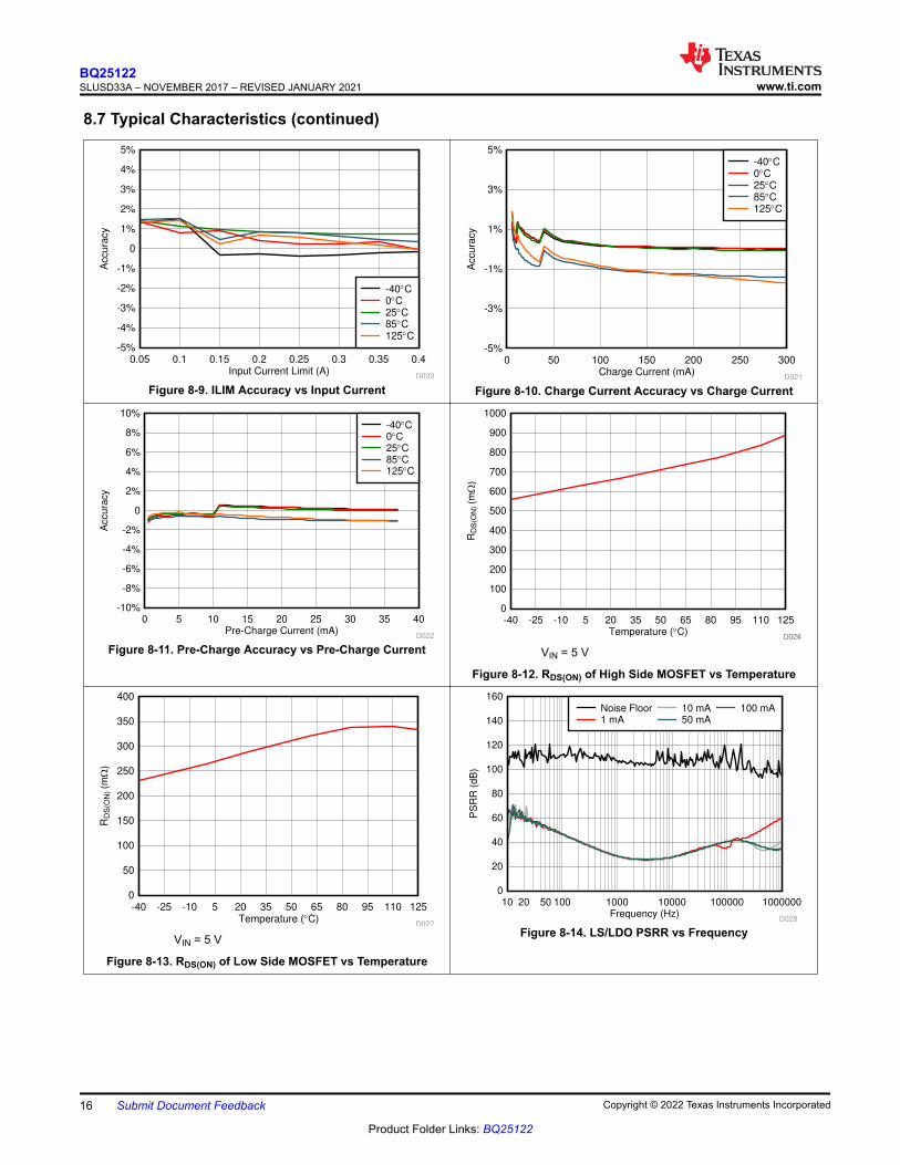
8.7 Typical Characteristics
BAT (V)
BA
T I
Q (P
A)
3 3.2 3.4 3.6 3.8 4 4.2 4.4 4.60
2
4
6
8
10
12
D016
85qC60qC
25qC0qC
Figure 8-3. Active BAT, IQ
BAT (V)
BA
T I
Q (P
A)
3 3.2 3.4 3.6 3.8 4 4.2 4.4 4.60.0
0.5
1.0
1.5
2.0
D017
85qC60qC
25qC0qC
1.8 V System Enabled (No Load)
Figure 8-4. Hi-Z BAT, IQ
BAT (V)
BA
T I
Q (P
A)
3 3.2 3.4 3.6 3.8 4 4.2 4.4 4.60.00
0.02
0.04
0.06
0.08
0.10
0.12
0.14
D018
85qC60qC
25qC0qC
Figure 8-5. Ship Mode BAT, IQ
Temperature (qC)
RD
S(O
N) (m:
)
-40 -25 -10 5 20 35 50 65 80 95 110 1250
100
200
300
400
500
600
700
D024
Figure 8-6. Blocking FET RDS(ON) vs Temperature
Temperature (qC)
RD
S(O
N) (m:
)
-40 -25 -10 5 20 35 50 65 80 95 110 1250
50
100
150
200
250
300
350
400
D025
Figure 8-7. Battery Discharge FET RDS(ON) vs Temperature
Temperature (qC)
Accura
cy
-40 -10 20 50 80 110 125-0.5%
-0.3%
-0.1%
0.1%
0.3%
0.5%
D019
4.35 V(BATREG)
4.2 V(BATREG)
4 V(BATREG)
3.8 V(BATREG)
3.6 V(BATREG)
Figure 8-8. V(BATREG) Accuracy vs Temperature
www.ti.comBQ25122
SLUSD33A – NOVEMBER 2017 – REVISED JANUARY 2021
Copyright © 2022 Texas Instruments Incorporated Submit Document Feedback 15
Product Folder Links: BQ25122
8.7 Typical Characteristics (continued)
Input Current Limit (A)
Accura
cy
0.05 0.1 0.15 0.2 0.25 0.3 0.35 0.4-5%
-4%
-3%
-2%
-1%
0
1%
2%
3%
4%
5%
D020
-40qC0qC25qC85qC125qC
Figure 8-9. ILIM Accuracy vs Input CurrentCharge Current (mA)
Accura
cy
0 50 100 150 200 250 300-5%
-3%
-1%
1%
3%
5%
D021
-40qC0qC25qC85qC125qC
Figure 8-10. Charge Current Accuracy vs Charge Current
Pre-Charge Current (mA)
Accura
cy
0 5 10 15 20 25 30 35 40-10%
-8%
-6%
-4%
-2%
0
2%
4%
6%
8%
10%
D022
-40qC0qC25qC85qC125qC
Figure 8-11. Pre-Charge Accuracy vs Pre-Charge CurrentTemperature (qC)
RD
S(O
N) (m:
)
-40 -25 -10 5 20 35 50 65 80 95 110 1250
100
200
300
400
500
600
700
800
900
1000
D026D024
VIN = 5 V
Figure 8-12. RDS(ON) of High Side MOSFET vs Temperature
Temperature (qC)
RD
S(O
N) (m:
)
-40 -25 -10 5 20 35 50 65 80 95 110 1250
50
100
150
200
250
300
350
400
D027
VIN = 5 V
Figure 8-13. RDS(ON) of Low Side MOSFET vs Temperature
Frequency (Hz)
PS
RR
(dB
)
10 20 50 100 1000 10000 100000 10000000
20
40
60
80
100
120
140
160
D028
Noise Floor1 mA
10 mA50 mA
100 mA
Figure 8-14. LS/LDO PSRR vs Frequency
BQ25122SLUSD33A – NOVEMBER 2017 – REVISED JANUARY 2021 www.ti.com
16 Submit Document Feedback Copyright © 2022 Texas Instruments Incorporated
Product Folder Links: BQ25122

9 Detailed Description9.1 OverviewThe following sections describe in detail the functions provided by the BQ25122. These include linear charger, PWM output, configurable LS/LDO output, Push-button input, reset timer, functional modes, battery monitor, I2C configurability and functions, and safety features.
9.2 Functional Block Diagram
SW
MR
TS
LS/LDO
BAT
PWM, LDO, and BAT FET Control
I2C Interface
Hi-Z Mode
Device Control
Reset andTimer
+
+
+
+
VIN
TS COLD
TS HOT
TS WARM
TS COOL
SYS
1C/ 0.5C
Disable
Disable
VBATREG ± 140mV
LDO/ Load SwitchControl
IINLIM
Q1/Q2 Q3
Q4
VIN_DPM
VSUPPLY
VBATREG
LDOControl
VSYSREG
Thermal
Shutdown
+
+
Termination Reference
IBAT
VIN
VINOVP VBAT
VBATOVP
VBATREG ± 0.12 V
VBAT
VBAT
VBATSHRT
IBATREG
+
+
+RESET
Q5
Q7
VOVP
BATOVP
BATSHRT
Recharge
PMID
LDO/ Load SwitchHost Control
Input Current Limit
Charge Current
Termination Current
PG
+ VBAT(SC)
SDA
SCL
LSCTRL
ILIM
ISET
IPRETERM
INT
GND
IN
VINLS
CD
Copyright © 2016, Texas Instruments Incorporated
S D
G
S
D
G
S
D
G
www.ti.comBQ25122
SLUSD33A – NOVEMBER 2017 – REVISED JANUARY 2021
Copyright © 2022 Texas Instruments Incorporated Submit Document Feedback 17
Product Folder Links: BQ25122

9.3 Feature Description9.3.1 Ship Mode
Ship Mode is the lowest quiescent current state for the device. Ship Mode latches off the device and BAT FET until VIN > VBAT + VSLP or the MR button is depressed for tWAKE1 and released. The following list shows the events that are active during Ship Mode:1. VIN_UV Comparator2. MR Input (No clock or delay in this mode for lowest power consumption)3. PMID active pull down
9.3.1.1 Ship Mode Entry and Exit
The device may only enter Ship Mode when there is not a valid VIN supply present (VIN < VUVLO). Once the IN supply is removed there are two ways for the device to enter Ship Mode: through I2C command using the EN_SHIPMODE bit and by doing a long button press when MRREC bit is set to 0. If the EN_SHIPMODE bit is set while the IN supply is present, the device will enter Ship Mode upon removal of the supply. The EN_SHIPMODE bit can be cleared using the I2C interface as well while the IN input is valid.
In addition to VIN < VUVLO, CD and MR must be high. Once all of these conditions are met the device will begin the transition to Ship Mode. All three conditions must remain unchanged for a period of tQUIET to ensure proper operation. Figure 9-1 and Figure 9-2 show the correct sequencing to ensure proper entry into the Ship Mode through I2C command and MR button press respectively.
VIN
MR
CD
Shipmode
I2C
Write xxxxxxxxxxxx
xx
tQUIET
Figure 9-1. CD, MR and VIN Sequencing for Ship Mode Entry Through I2C Command
VIN
MR
CD
Shipmode
I2C
Write xxxxxxxxxxxx
t > tRESET
tQUIET
Figure 9-2. CD, MR and VIN Sequencing for Ship Mode Entry Through Long MR button press
BQ25122SLUSD33A – NOVEMBER 2017 – REVISED JANUARY 2021 www.ti.com
18 Submit Document Feedback Copyright © 2022 Texas Instruments Incorporated
Product Folder Links: BQ25122

The end user can enable the device (exit Ship Mode) by connecting an adapter to IN (VIN > VBAT + VSLP) or by toggling the MR button. Note that in the case where an adapter is connected while the MR is still held low and immediately after the RESET timer has expired ( MR low for tRESET), the device will not enter Ship Mode, but may enter it upon adapter removal (Same behavior as setting the EN_SHIPMODE bit when the adapter is present). This will not be the case if MR has gone high when the adapter is connected or MR continues to be held low for a period longer than tWAKE1 after the adapter is connected.
To exit Ship Mode through and MR press the battery voltage must be above the maximum programmable BUVLO threshold when VIN is not present. Once MR goes low, the device will start to exit Ship Mode, powering PMID. The device will not complete the transition from Ship Mode until MR has been held low for at least tWAKE1. Only after the transition is complete may the host start I2C communication if the device has not entered High Impedance Mode.
9.3.2 High Impedance Mode
High Impedance mode is the lowest quiescent current state while operating from the battery. During Hi-Z mode the SYS output is powered by BAT, the MR input is active, and the LSCTRL input is active. All other circuits are in a low power or sleep state.The LS/LDO output can be enabled in Hi-Z mode with the LSCTRL input. If the LS/LDO output has been enabled through I2C prior to entering Hi-Z mode, it will stay enabled. The CD pin is used to put the device in a high-impedance mode when battery is present and VIN < VUVLO. Drive CD high to enable the device and enter active battery operation when VIN is not valid. When the HZ_MODE bit is written by the host, the I2C interface is disabled if only battery is present. To resume I2C, the CD pin must be toggled. If the supply for the CD pull up glitches or experiences a brownout condition , it is recommended to toggle the /CD pin to resume I2C communication.. The functionality of the pin is shown in Table 9-1.
Table 9-1. CD, State TableCD, STATE VIN < VUVLO VIN > VUVLO
L Hi-Z Charge Enabled
H Active Battery Charge Disabled
9.3.3 Active Battery Only Connected
When the battery above VBATUVLO is connected with no input source, the battery discharge FET is turned on. After the battery rises above VBATUVLO and the deglitch time is reached, the SYS output starts to rise. The current from PMID and SYS is not regulated, but is protected by a short circuit current limit. If the short circuit limit is reached for the deglitch time (tDGL_SC), the battery discharge FET is turned off for the recovery time (tREC_SC). After the recovery time, the battery FET is turned on to test if the short has been removed. If it has not, the FET turns off and the process repeats until the short is removed. This process protects the internal FET from over current. During this event PMID will likely droop and cause SYS to go out of regulation.
To provide designers the most flexibility in optimizing their system, an adjustable BATUVLO is provided. When the voltage drops below the VBATUVLO threshold, the battery discharge FET is turned off. Deeper discharge of the battery enables longer times between charging, but may shorten the battery life. The BATUVLO is adjustable with a fixed 150-mV hysteresis.
If a valid VIN is connected during active battery mode, VIN > VUVLO, the supplement and battery discharge FET is turned on when the battery voltage is above the minimum VBATUVLO.
Drive CD high or write the CE register to disable charge when VIN > VUVLO is present. CD is internally pulled down. When exiting this mode, charging resumes if VIN is present, CD is low and charging is enabled.
All HOST interfaces ( CD, SDA/SCL, INT, RESET and LSCTRL) are active no later than 5 ms after SYS reaches the programmed level.
9.3.4 Voltage Based Battery Monitor
The device implements a simple voltage battery monitor which can be used to determine the depth of discharge. Prior to entering High-Z mode, the device will initiate a VBMON reading. The host can read the latched value for the no-load battery voltage, or initiate a reading using VBMON_READ to see the battery voltage under a known load. The register will be updated and can be read 2ms after a read is initiated. The VBMON voltage threshold is
www.ti.comBQ25122
SLUSD33A – NOVEMBER 2017 – REVISED JANUARY 2021
Copyright © 2022 Texas Instruments Incorporated Submit Document Feedback 19
Product Folder Links: BQ25122

readable with 2% increments with ±1.5% accuracy between 60% and 100% of VBATREG using the VBMON_TH registers. Reading the value during charge is possible, but for the most accurate battery voltage indication, it is recommended to disable charge, initiate a read, and then re-enable charge.
A typical discharge profile for a Li-Ion battery is shown in Table 9-2. The specific battery to be used in the application should be fully characterized to determine the thresholds that will indicate the appropriate battery status to the user. Two typical examples are shown below, assuming the VBMON reading is taken with no load on the battery.
This function enables a simple 5-bar status indicator with the following typical performance with different VBATREG settings:
Table 9-2. Discharge Profile for a Li-Ion BatteryVBATREG BATTERY FULL 95% to 65%
REMAINING CAPACITY65% to 35%
REMAINING CAPACITY35% to 5%
REMAINING CAPACITY BATTERY EMPTY
4.35 V VBMON > 90% VBMON = 88% VBMON = 86% VBMON = 84% VBMON < 82%
4.2 V VBMON > 98% VBMON = 94% or 96% VBMON = 90% or 92% VBMON = 86% or 88% VBMON < 84%
D
E
C
O
D
E
R
S 3
S 2
S 1
S 0 - 2 % BAT TAP
- 4 % BAT TAP
- 6 % BAT TAP
- 8 % BAT TAP
- 10 % BAT TAP
VREF
90 % VB
80 % VB
70 % VB
60 % VB
VB = 0 . 8 VBAT
VB
GU
AG
E_
TH
<2
:0>
Figure 9-3. Voltage Battery Monitor
9.3.5 Sleep Mode
The device enters the low-power sleep mode if the voltage IN falls below the sleep-mode entry threshold and VIN is higher than the undervoltage lockout threshold. In sleep mode, the input is isolated from the connected battery. This feature prevents draining the battery during the absence of VIN. When VIN < V(BAT) + VSLP, the device turns the battery discharge FET on, sends a 128-µs pulse on the INT output, and the FAULT bits of the register are update over I2C. Once VIN > V(BAT) + VSLP, the device initiates a new charge cycle. The FAULT bits are not cleared until they are read over I2C and the sleep condition no longer exists. It is not recommended to do a battery connection or plug in when VUVLO< VIN < VBAT + VSLP as it may cause higher quiescent current to be drained form the battery.
BQ25122SLUSD33A – NOVEMBER 2017 – REVISED JANUARY 2021 www.ti.com
20 Submit Document Feedback Copyright © 2022 Texas Instruments Incorporated
Product Folder Links: BQ25122

9.3.6 Input Voltage Based Dynamic Power Management (VIN(DPM))
During the normal charging process, if the input power source is not able to support the programmed or default charging current and System load, the supply voltage decreases. Once the supply approaches VIN(DPM), the input DPM current and voltage loops will reduce the input current through the blocking FETs, to prevent the further drop of the supply. The VIN(DPM) threshold is programmable through the I2C register from 4.2 V to 4.9 V in 100-mV steps. It can be disabled completely as well. When the device enters this mode, the charge current may be lower than the set value and the VINDPM_STAT bit is set. If the 2X timer is set, the safety timer is extended while VIN(DPM) is active. Additionally, termination is disabled. Note that in a condition where the battery is connected while VUVLO<VIN < VIN(DPM), the VINDPM loop will prevent the battery from being charged and PMID will be powered from BAT.
9.3.7 Input Overvoltage Protection and Undervoltage Status Indication
The input overvoltage protection protects the device and downstream components connected to PMID, SYS, and BAT against damage from overvoltage on the input supply. When VIN > VOVP an OVP fault is determined to exist. During the OVP fault, the device turns the battery discharge FET on, sends a single 128-µs pulse on INT, and the FAULT bits are updated over I2C. Once the OVP fault is removed, after the deglitch time, tDGL_OVP, STAT and FAULT bits are cleared and the device returns to normal operation. The FAULT bits are not cleared until they are read in from I2C after the OVP condition no longer exists. The OVP threshold for the device is set to operate from standard USB sources.
The input under-voltage status indication is used to notify the host or other device when the input voltage falls below a desired threshold. When VIN < VUVLO, after the deglitch time tDGL_UVLO, a UVLO fault is determined to exist. During the VIN UVLO fault, the device sends a single 128-µs pulse on INT, and the STAT and FAULT bits are updated over I2C. The FAULT bits are not cleared until they are read in from I2C after the UVLO condition no longer exists.
9.3.8 Battery Charging Process and Charge Profile
When a valid input source is connected (VIN > VUVLO and V(BAT) + VSLP < VIN < VOVP and VIN > VIN(DPM)), the CE bit in the control register determines whether a charge cycle is initiated. When the CE bit is 1 and a valid input source is connected, the battery discharge FET is turned off, and the output at SYS is regulated depending on the output configuration. A charge cycle is initiated when the CE bit is written to a 0. Alternatively, the CD input can be used to enable and disable charge.
The device supports multiple battery chemistries for single-cell applications. Charging is done through the internal battery MOSFET. There are several loops that influence the charge current: constant current loop (CC), constant voltage loop (CV), input current limit, VDPPM, and VIN(DPM). During the charging process, all loops are enabled and the one that is dominant takes control.
The charge current is regulated to ICHARGE until the voltage between BAT and GND reaches the regulation voltage. The voltage between BAT and GND is regulated to VBATREG (CV Mode) while the charge current naturally tapers down. When termination is enabled, the device monitors the charging current during the CV mode, and once the charge current tapers down to the termination threshold, ITERM, and the battery voltage is above the recharge threshold, the device terminates charge, and turns off the battery charging FET. Termination is disabled when any loop is active other than CV.
9.3.9 Dynamic Power Path Management Mode
With a valid input source connected, the power-path management circuitry monitors the input voltage and current continuously. The current into IN is shared at PMID between charging the battery and powering the system load at PMID, SYS, and LS/LDO. If the sum of the charging and load currents exceeds the current that the VIN can support, the input DPM loop (VINDPM) reduces the current going into PMID through the input blocking FETs. This will cause a drop on the PMID voltage if the system demands more current. If PMID drops below the DPPM voltage threshold (VDPPM), the charging current is reduced by the DPPM loop through the BATFET in order to stabilize PMID. If PMID continues to drop after BATFET charging current is reduced to zero, the part enters supplement mode when PMID falls below the supplement mode threshold. Battery termination is disabled while in DPPM mode. In order to charge the battery, the voltage at PMID has to be greater than VBATREG + VDPPM threshold.
www.ti.comBQ25122
SLUSD33A – NOVEMBER 2017 – REVISED JANUARY 2021
Copyright © 2022 Texas Instruments Incorporated Submit Document Feedback 21
Product Folder Links: BQ25122
9.3.10 Battery Supplement Mode
While in DPPM mode, if the charging current falls to zero and the system load current increases beyond the programmed input current limit, the voltage at PMID reduces further. When the PMID voltage drops below the battery voltage by V(BSUP1), the battery supplements the system load. The battery stops supplementing the system load when the voltage on the PMID pin rises above the battery voltage by V(BSUP2). During supplement mode, the battery supplement current is not regulated, however, the short-circuit protection circuit is active. Battery termination is disabled while in supplement mode.
9.3.11 Default Mode
The default mode is used when there is no host, or I2C communication is not available. If the externally programmable pins, ILIM, ISET, and ITERM have resistors connected, that is considered the default mode. If any one of these resistors is tied to GND, the default register settings are used. The default mode can be entered by connecting a valid power source to VIN or the RESET bit is written. Default mode is exited by writing to the I2C interface.
9.3.12 Termination and Pre-Charge Current Programming by External Components (IPRETERM)
The termination current threshold is user programmable through an external resistor or through registers over I2C. Set the termination current using the IPRETERM pin by connecting a resistor from IPRETERM to GND. The termination can be set between 5% and 20% of the programmed output current set by ISET, using Table 9-3 for guidance:
Table 9-3. IPRETERM Resistor Settings
IPRE_CHARGE and ITERM KKIPRETERMRIPRETERM
(STANDARD 1% VALUES) UNIT
MIN TYP(% of ISET) MAX MIN TYP MAX RECOMMENDED
RIPRETERM
5 180 200 220 15000 Ω
10 180 200 220 4990 Ω
15 180 200 220 1650 Ω
20 180 200 220 549 Ω
Using the I2C register, the termination current can be programmed with a minimum of 500 µA and a maximum of 37 mA.
The pre-charge current is not independently programmable through the external resistor, and is set at the termination current. The pre-charge and termination currents are programmable using the IPRETERM registers. If no IPRETERM resistor is connected and the pin is tied to GND, the default values in the IPRETERM registers are used. The external value can be used in host mode by configuring the IPRETERM registers. If the external ICHG setting will be used after being in Host mode, the IPRETERM registers should be set to match the desired external threshold for the highest ICHG accuracy.
Termination is disabled when any loop other than CV is active.
BQ25122SLUSD33A – NOVEMBER 2017 – REVISED JANUARY 2021 www.ti.com
22 Submit Document Feedback Copyright © 2022 Texas Instruments Incorporated
Product Folder Links: BQ25122
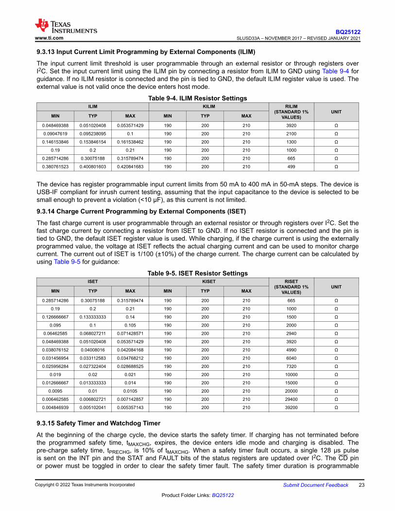
9.3.13 Input Current Limit Programming by External Components (ILIM)
The input current limit threshold is user programmable through an external resistor or through registers over I2C. Set the input current limit using the ILIM pin by connecting a resistor from ILIM to GND using Table 9-4 for guidance. If no ILIM resistor is connected and the pin is tied to GND, the default ILIM register value is used. The external value is not valid once the device enters host mode.
Table 9-4. ILIM Resistor SettingsILIM KILIM RILIM
(STANDARD 1% VALUES)
UNITMIN TYP MAX MIN TYP MAX
0.048469388 0.051020408 0.053571429 190 200 210 3920 Ω
0.09047619 0.095238095 0.1 190 200 210 2100 Ω
0.146153846 0.153846154 0.161538462 190 200 210 1300 Ω
0.19 0.2 0.21 190 200 210 1000 Ω
0.285714286 0.30075188 0.315789474 190 200 210 665 Ω
0.380761523 0.400801603 0.420841683 190 200 210 499 Ω
The device has register programmable input current limits from 50 mA to 400 mA in 50-mA steps. The device is USB-IF compliant for inrush current testing, assuming that the input capacitance to the device is selected to be small enough to prevent a violation (<10 µF), as this current is not limited.
9.3.14 Charge Current Programming by External Components (ISET)
The fast charge current is user programmable through an external resistor or through registers over I2C. Set the fast charge current by connecting a resistor from ISET to GND. If no ISET resistor is connected and the pin is tied to GND, the default ISET register value is used. While charging, if the charge current is using the externally programmed value, the voltage at ISET reflects the actual charging current and can be used to monitor charge current. The current out of ISET is 1/100 (±10%) of the charge current. The charge current can be calculated by using Table 9-5 for guidance:
Table 9-5. ISET Resistor SettingsISET KISET RISET
(STANDARD 1% VALUES)
UNITMIN TYP MAX MIN TYP MAX
0.285714286 0.30075188 0.315789474 190 200 210 665 Ω
0.19 0.2 0.21 190 200 210 1000 Ω
0.126666667 0.133333333 0.14 190 200 210 1500 Ω
0.095 0.1 0.105 190 200 210 2000 Ω
0.06462585 0.068027211 0.071428571 190 200 210 2940 Ω
0.048469388 0.051020408 0.053571429 190 200 210 3920 Ω
0.038076152 0.04008016 0.042084168 190 200 210 4990 Ω
0.031456954 0.033112583 0.034768212 190 200 210 6040 Ω
0.025956284 0.027322404 0.028688525 190 200 210 7320 Ω
0.019 0.02 0.021 190 200 210 10000 Ω
0.012666667 0.013333333 0.014 190 200 210 15000 Ω
0.0095 0.01 0.0105 190 200 210 20000 Ω
0.006462585 0.006802721 0.007142857 190 200 210 29400 Ω
0.004846939 0.005102041 0.005357143 190 200 210 39200 Ω
9.3.15 Safety Timer and Watchdog Timer
At the beginning of the charge cycle, the device starts the safety timer. If charging has not terminated before the programmed safety time, tMAXCHG, expires, the device enters idle mode and charging is disabled. The pre-charge safety time, tPRECHG, is 10% of tMAXCHG. When a safety timer fault occurs, a single 128 µs pulse is sent on the INT pin and the STAT and FAULT bits of the status registers are updated over I2C. The CD pin or power must be toggled in order to clear the safety timer fault. The safety timer duration is programmable
www.ti.comBQ25122
SLUSD33A – NOVEMBER 2017 – REVISED JANUARY 2021
Copyright © 2022 Texas Instruments Incorporated Submit Document Feedback 23
Product Folder Links: BQ25122

using the TMR bits. When the safety timer is active, changing the safety timer duration resets the safety timer. The device also contains a 2X_TIMER bit that enables the 2X timer function to prevent premature safety timer expiration when the charge current is reduced by a load on PMID, SYS, LS/LDO or a NTC condition. When t2X_TIMER function is enabled, the timer is allowed to run at half speed when any loop is active other than CC or CV.
In addition to the safety timer, the device contains a 50-second watchdog timer that monitors the host through the I2C interface. Only after an I2C transaction is performed on the I2C interface, will the watchdog timer start. In the case where the device is set to operate in High Impedance Mode, the watchdog timer is automatically disabled and can only be re-started after the device exits the High Impedance Mode and a subsequent I2C transaction is performed. The watchdog timer is reset by any transaction by the host using the I2C interface. If the watchdog timer expires without a reset from the I2C interface, all registers except MRRESET_VIN and MRREC are reset to the default values.
9.3.16 External NTC Monitoring (TS)
The I2C interface allows the user to easily implement the JEITA standard for systems where the battery pack thermistor is monitored by the host. Additionally, the device provides a flexible voltage based TS input for monitoring the battery pack NTC thermistor. The voltage at TS is monitored to determine that the battery is at a safe temperature during charging.
To satisfy the JEITA requirements, four temperature thresholds are monitored: the cold battery threshold, the cool battery threshold, the warm battery threshold, and the hot battery threshold. These temperatures correspond to the V(COLD), V(COOL), V(WARM), and V(HOT) threshold in the Section 8.5. Charging and timers are suspended when V(TS) < V(HOT) or > V(COLD). When V(COOL) < V(TS) < V(COLD), the charging current is reduced to half of the programmed charge current. When V(HOT) < V(TS) < V(WARM), the battery regulation voltage is reduced by 140 mV (minimum VBATREG under this condition is 3.6V).
The TS function is voltage based for maximum flexibility. Connect a resistor divider from VIN to GND with TS connected to the center tap to set the threshold. The connections are shown in Figure 9-4. The resistor values are calculated using Equation 1 and Equation 2. To disable the TS function, pull TS above TSOFF threshold.
DISABLE
TEMPPACK+
PACK–
+
+
+
+
VDRV
TS COLD
TS HOT
TS WARM
TS COOL
VBATREG
– 140 mV
TS
BQ25122
RHI
RLO
1 x Charge/0.5 x Charge
VDRV
Figure 9-4. TS Circuit
BQ25122SLUSD33A – NOVEMBER 2017 – REVISED JANUARY 2021 www.ti.com
24 Submit Document Feedback Copyright © 2022 Texas Instruments Incorporated
Product Folder Links: BQ25122

IN (COLD) (HOT)(COLD) (HOT)
(LO)IN IN
(HOT) (COLD)(HOT) (COLD)
1 1V x R x R x
V VR =
V VR x 1 R x 1
V V
æ öç ÷-ç ÷è ø
æ ö æ öç ÷ ç ÷- - -ç ÷ ç ÷è ø è ø (1)
IN
(COLD)(HI)
(LO) (COLD)
V1
VR =
1 1+
R R
æ öç ÷-ç ÷è ø
æ öç ÷ç ÷è ø (2)
Where• R(HOT) = the NTC resistance at the hot temperature• R(COLD) = the NTC resistance at the cold temperature
The warm and cool thresholds are not independently programmable. The cool and warm NTC resistances for a selected resistor divider are calculated using Equation 3 and Equation 4.
(LO) (HI) COOL(COOL)
(LO) (LO) COOL (HI) COOL
R x R x VR =
R R x V R x V- - (3)
( )(LO) (HI) WARM(WARM) (LO) WARM (HI) WARM
(LO)
R x R x VR = R x V R x V
R- -
(4)
www.ti.comBQ25122
SLUSD33A – NOVEMBER 2017 – REVISED JANUARY 2021
Copyright © 2022 Texas Instruments Incorporated Submit Document Feedback 25
Product Folder Links: BQ25122

9.3.17 Thermal Protection
During the charging process, to prevent overheating in the device, the juntion temperature of the die, TJ, is monitored. When TJ reaches T(SHUTDOWN) the device stops charging, disables the PMID output, disables the SYS output, and disables the LS/LDO output. During the time that T(SHUTDOWN) is exceeded, the safety timer is reset and the watchdog timer continues to operate if in host mode. The charge cycle resumes when TJ falls below T(SHUTDOWN) by T(HYS).
To avoid reaching thremal shutdown, ensure that the system power dissipation is under the limits of the device. The power dissipated by the device can be calculated using Equation 5.
PDISS = P(BLOCK) + P(SYS) + P(LS/LDO) + P(BAT) (5)
Where• P(BLOCK) = (VIN – V(PMID)) x IIN• P(SYS) = ISYS 2 x RDS(ON_HS)• P(LS/LDO) = (V(INLS) – V(LS/LDO)) x I(LS/LDO)• P(BAT) = (V(PMID) – V(BAT)) x I(BAT)
9.3.18 Typical Application Power Dissipation
The die junction temperature, TJ, can be estimated based on the expected board performance using Equation 6.
TJ = TA + θJA x PDISS (6)
The θJA is largely driven by the board layout. For more information about traditional and new thermal metrics, see the IC Package Thermal Metrics application report SPRA953. Under typical conditions, the time spent in this state is short.
9.3.19 Status Indicators ( PG and INT)
The device contains two open-drain outputs that signal its status and are valid only after the device has completed start-up into a valid state. If the part starts into a fault, interrupts will not be sent. The PG output signals when a valid input source is connected. PG pulls to GND when VIN > VUVLO, VIN> VBAT+VSLP and VIN < VOVP. PG is high-impedance when the input power is not within specified limits. Connect PG to the desired logic voltage rail using a 1-kΩ to 100-kΩ resistor, or use with an LED for visual indication.
The PG pin can be configured as a MR shifted (MRS) output when the PGB_MRS bit is set to 1. PG is high-impedance when the MR input is not low, and PG pulls to GND when the MR input is below VOL(TH_MRS). Connect PG to the desired logic voltage rail using a 1-kΩ to 100-kΩ resistor.
The INT pin is pulled low during charging when the EN_INT bit is set to 1 and interrupts are pulled high. When EN_INT is set to 0, charging status is not indicated on the INT pin. When charge is complete or disabled, INT is high impedance. The charge status is valid whether it is the first charge or recharge. When a fault occurs, a 128 µs pulse (interrupt) is sent on INT to notify the host.
9.3.20 Chip Disable ( CD)
The device contains a CD input that is used to disable the device and place it into a high impedance mode when only battery is present. In this case, when CD is low, PMID and SYS remain active, and the battery discharge FET is turned on. If the LS/LDO output has been enabled prior to pulling CD low, it will stay on. The LSCTRL pin can also enable/disable the LS/LDO output when the CD pin is pulled low. The CD pin has an internal pull-down.
If VIN is present and the CD input is pulled low, charge is enabled and all other functions remain active. If VIN is present and the CD input is pulled high, charge is disabled.
9.3.21 Buck (PWM) Output
The device integrates a low quiscent current switching regulator with DCS control allowing high efficiency down to 10-µA load currents. DCS control combines the advantages of hysteretic and voltage mode control. The internally compensated regulation network achieves fast and stable operation with small external components and low ESR capacitors. During PWM mode, it operates in continuous conduction mode, with a frequency up to
BQ25122SLUSD33A – NOVEMBER 2017 – REVISED JANUARY 2021 www.ti.com
26 Submit Document Feedback Copyright © 2022 Texas Instruments Incorporated
Product Folder Links: BQ25122
2 MHz. If the load current decreases, the converter enters a power save mode to maintain high efficiency down to light loads. In this mode, the device generates a single switching pulse to ramp up the inductor current and recharge the output capacitor, followed by a sleep period where most of the internal circuits are shut down to achieve a low quiescent current. The duration of the sleep period depends on the load current and the inductor peak current. For optimal operation and maximum power delivery allow VPMID > VSYS + 0.7V.
The output voltage is programmable using the SYS_SEL and SYS_VOUT bits in the SYS VOUT control register.
The SW output is enabled using the EN_SYS_OUT bit in the register. This bit is for testing and debug only and not intended to be used in the final system. When the device is enabled, the internal reference is powered up and the device enters softstart, starts switching, and ramps up the output voltage. When SW is disabled, the output is in shutdown mode in a low quiescent state. The device provides automatic output voltage discharge so the output voltage will ramp up from zero once the device in enabled again. Once SYS has been disabled, either VIN needs to be connected or the MR button must be held low for the tRESET duration to re-enable SYS.
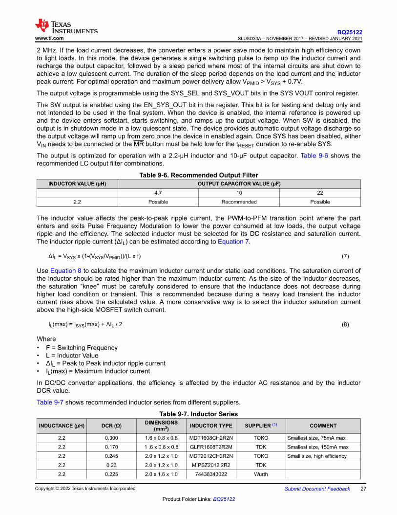
The output is optimized for operation with a 2.2-µH inductor and 10-µF output capacitor. Table 9-6 shows the recommended LC output filter combinations.
Table 9-6. Recommended Output FilterINDUCTOR VALUE (µH) OUTPUT CAPACITOR VALUE (µF)
4.7 10 22
2.2 Possible Recommended Possible
The inductor value affects the peak-to-peak ripple current, the PWM-to-PFM transition point where the part enters and exits Pulse Frequency Modulation to lower the power consumed at low loads, the output voltage ripple and the efficiency. The selected inductor must be selected for its DC resistance and saturation current. The inductor ripple current (ΔIL) can be estimated according to Equation 7.
ΔIL = VSYS x (1-(VSYS/VPMID))/(L x f) (7)
Use Equation 8 to calculate the maximum inductor current under static load conditions. The saturation current of the inductor should be rated higher than the maximum inductor current. As the size of the inductor decreases, the saturation “knee” must be carefully considered to ensure that the inductance does not decrease during higher load condition or transient. This is recommended because during a heavy load transient the inductor current rises above the calculated value. A more conservative way is to select the inductor saturation current above the high-side MOSFET switch current.
IL(max) = ISYS(max) + ΔIL / 2 (8)
Where• F = Switching Frequency• L = Inductor Value• ΔIL = Peak to Peak inductor ripple current• IL(max) = Maximum Inductor current
In DC/DC converter applications, the efficiency is affected by the inductor AC resistance and by the inductor DCR value.
Table 9-7 shows recommended inductor series from different suppliers.
Table 9-7. Inductor SeriesINDUCTANCE (µH) DCR (Ω) DIMENSIONS
(mm3) INDUCTOR TYPE SUPPLIER (1) COMMENT
2.2 0.300 1.6 x 0.8 x 0.8 MDT1608CH2R2N TOKO Smallest size, 75mA max
2.2 0.170 1 .6 x 0.8 x 0.8 GLFR1608T2R2M TDK Smallest size, 150mA max
2.2 0.245 2.0 x 1.2 x 1.0 MDT2012CH2R2N TOKO Small size, high efficiency
2.2 0.23 2.0 x 1.2 x 1.0 MIPSZ2012 2R2 TDK
2.2 0.225 2.0 x 1.6 x 1.0 74438343022 Wurth
www.ti.comBQ25122
SLUSD33A – NOVEMBER 2017 – REVISED JANUARY 2021
Copyright © 2022 Texas Instruments Incorporated Submit Document Feedback 27
Product Folder Links: BQ25122

Table 9-7. Inductor Series (continued)INDUCTANCE (µH) DCR (Ω) DIMENSIONS
(mm3) INDUCTOR TYPE SUPPLIER (1) COMMENT
2.2 0.12 2.5 x 2.0 x 1.2 MIPSA2520 2R2 TDK
2.2 0.145 3.3 x 3.3 x 1.4 LPS3314 Coicraft
(1) See Third-party Products Disclaimer
The PWM allows the use of small ceramic capacitors. Ceramic capacitors with low ESR values have the lowest output voltage ripple and are recommended. The output capacitor requires either an X7R or X5R dielectric. At light load currents, the converter operates in Power Save Mode and the output voltage ripple is dependent on the output capacitor value and the PFM peak inductor current. Because the PWM converter has a pulsating input current, a low ESR input capacitor is required on PMID for the best voltage filtering to ensure proper function of the device and to minimize input voltage spikes. For most applications a 10-µF capacitor value is sufficient. The PMID capacitor can be increased to 22 µF for better input voltage filtering.
Table 9-8 shows the recommended input/output capacitors.
Table 9-8. CapacitorsCAPACITANCE (µF) SIZE CAPACITOR TYPE SUPPLIER(1) COMMENT
10 0603 GRM188R60J106ME84 Murata Recommended
10 0402 CL05A106MP5NUNC Samsung EMA Smallest size
(1) See Third-party Products Disclaimer
9.3.22 Load Switch / LDO Output and Control
The device integrates a low Iq load switch which can also be used as a regulated output. The LSCTRL pin can be used to turn the load on or off. Activating LSCTRL continuously holds the switch in the on state so long as there is not a fault. The signal is active HI and has a low threshold making it capable of interfacing with low voltage signals. To limit voltage drop or voltage transients, a small ceramic capacitor must be placed close to VINLS. Due to the body diode of the PMOS switch, it is recommended to have the capacitor on VINLS ten times larger than the output capacitor on LS/LDO.
The output voltage is programmable using the LS_LDO bits in the register. The LS/LDO voltage is calculated using Equation 9.
LS/LDO = 0.8 V + LS_LDOCODE x 100 mV (9)
If a value greater than 3.3 V is written, the setting goes to pass-through mode where LS/LDO = VINLS - V(DROPOUT). Table 9-9 summarizes the control of the LS/LDO output based on the I2C or LSCTRL pin setting:
Table 9-9. LS/LDO Output ControlI2C LS_LDO_EN PIN LSCTRL I2C VLDO > 3.3 LS/LDO OUTPUT
0 0 0 Pulldown
0 0 1 Pulldown
0 1 0 VLDO
0 1 1 LSW
1 0 0 VLDO
1 0 1 LSW
1 1 0 VLDO
1 1 1 LSW
If the output of the LDO is less than the programmed V(SYS) voltage, connect VINLS to SYS. If the output of the LDO is greater than the programmed VSYS voltage, connect VINLS to PMID.
BQ25122SLUSD33A – NOVEMBER 2017 – REVISED JANUARY 2021 www.ti.com
28 Submit Document Feedback Copyright © 2022 Texas Instruments Incorporated
Product Folder Links: BQ25122
The current capability of the LDO depends on the VINLS input voltage and the programmed output voltage. The full 100-mA output current for 0.8-V output voltage can be achieved when V(VINLS) > 3.25 V. The full 100-mA output current for 3.3-V output voltage can be achieved when V(VINLS) > 3.6 V.
When the LSLDO output is disabled with LSCTRL or through the register, an internal pull-down discharges the output.
9.3.23 Manual Reset Timer and Reset Output ( MR and RESET)
The MR input has an internal pull-up to BAT, and MR is functional only when BAT is present or when VIN is valid, stable, and charge is enabled. If MR input is asserted during a transient condition while VIN ramps up the IC may incorrectly turn off the SYS buck output, therefore MR should not be asserted during this condition in order to avoid unwanted shutdown of SYS output rail.The input conditions can be adjusted by using MRWAKE bits for the wake conditions and MRRESET bits for the reset conditions. When a wake condition is met, a 128-µs pulse is sent on INT to notify the host, and the WAKE1 and/or WAKE2 bits are updated on I2C. The MR_WAKE bits and RESET FAULT bits are not cleared until the Push-button Control Register is read from I2C.
When a MR reset condition is met, a 128us pulse is sent on INT to notify the host and a RESET signal is asserted. A reset pulse occurs with duration of tRESET_D only one time after each valid MRRESET condition. The MR pin must be released (go high) and then driven low for the MRWAKE period before RESET asserts again. After RESET is asserted with battery only present, the device enters either Ship mode or Hi-Z mode depending on MRREC register settings. For details on how to properly enter Ship Mode through MR, see Section 9.3.1.1. After RESET is asserted with a valid VIN present, the device resumes operation prior to the MR button press. If SYS was disabled prior to RESET, the SYS output is re-enabled if recovering into Hi-Z or Active Battery.
The MRRESET_VIN register can be configured to have RESET asserted by a button press only, or by a button press and VIN present (VUVLO + VSLP < VIN < VOVP).
www.ti.comBQ25122
SLUSD33A – NOVEMBER 2017 – REVISED JANUARY 2021
Copyright © 2022 Texas Instruments Incorporated Submit Document Feedback 29
Product Folder Links: BQ25122

9.4 Device Functional ModesTable 9-10. Modes and Functions
FUNCTIONREADY (PRIOR
TO I2C) AND AFTER RESET
HOST MODE READY (AFTER
I2C)CHARGE SHIP MODE HIGH_Z ACTIVE
BATTERY
VOVP Yes Yes Yes No No No
VUVLO Yes Yes Yes Yes Yes Yes
VBATUVLO Yes Yes Yes No Yes Yes
VINDPM Default or registers
Default or registers If enabled No No No
SYS Default or registers
Default or registers If enabled No If enabled If enabled
LS/LDO Default or registers
Default or registers If enabled No If enabled If enabled
BATFET Yes Yes Yes No Yes Yes
TS Yes (VIN Valid) Yes (VIN Valid) Yes No No No
IPRETERM External Default, registers, or external
Default, registers, or external No No No
ISET External Default, registers, or external
Default, registers, or external No No No
ILIM External Default, registers, or external
Default, registers, or external No No No
MR input Yes Yes Yes Yes Yes Yes
LSCTRL input Yes Yes Yes No Yes Yes
RESET output Yes Yes Yes No Yes Yes
INT output Yes Yes Yes No No Yes
I2C interface Yes Yes Yes No No Yes
CD input Yes Yes Yes No Yes Yes
PG output Yes Yes Yes No No If enabled
VBMON No Yes No No No Yes
Table 9-11. Fault and Status Condition ResponsesFAULT or STATUS ACTIONS CHARGER
BEHAVIOR SYS BEHAVIOR LS/LDO BEHAVIOR TS BEHAVIOR
VIN_OVUpdate VIN_OV status,
Update STAT to fault, interrupt on INT, PG shown not good
Disabled Enabled through BAT
Enabled through BAT Disabled
VIN_UVUpdate VIN_UV status, on
interrupt on INT, PG shown not good
Disabled Enabled through BAT
Enabled through BAT Disabled
VIN_ILIMUpdate charge in progress
status, interrupt on INT, input current is limited
Enabled, input current limited Enabled (if enabled) Enabled (if enabled) Enabled
OVER_TEMP Disabled Disabled Disabled Disabled
BAT_UVLOUpdate BAT_UVLO status,
Update STAT to fault, interrupt on INT
Pre-charge Enabled (if enabled) and VIN Valid
Enabled (if enabled) and VIN Valid Enabled if VIN Valid
SW_SYS_SHORT Enabled Current Limit Enabled (if enabled) Enabled
LS_LDO_OCP Enabled Enabled (if enabled) Current Limit Enabled
TIMER fault Update TIMER, Update STAT to fault, interrupt on INT Disabled Enabled (if enabled) Enabled (if enabled) Disabled
VINDPMUpdate VINDPM_STAT,
Update STAT to fault, interrupt on INT
Enabled, input current reduced Enabled (if enabled) Enabled (if enabled) Enabled
BQ25122SLUSD33A – NOVEMBER 2017 – REVISED JANUARY 2021 www.ti.com
30 Submit Document Feedback Copyright © 2022 Texas Instruments Incorporated
Product Folder Links: BQ25122

Table 9-11. Fault and Status Condition Responses (continued)FAULT or STATUS ACTIONS CHARGER
BEHAVIOR SYS BEHAVIOR LS/LDO BEHAVIOR TS BEHAVIOR
TS_FAULT COLD or HOT
Update TS_FAULT to COLD OR HOT, Update STAT to fault,
interrupt on INTDisabled Enabled (if enabled) Enabled (if enabled) Enabled
TS_FAULT COOLUpdate TS_FAULT to COOL, Update STAT to fault, interrupt
on INTReduce ICHG to ½ Enabled (if enabled) Enabled (if enabled) Enabled
TS_FAULT WARMUpdate TS_FAULT to WARM, Update STAT to fault, interrupt
on INT
Reduce VBATREG by 140 mV Enabled (if enabled) Enabled (if enabled) Enabled
Charge Done Update STAT to Charge Done, interrupt on INT
Disabled, monitor for VBAT falling below VRCHG
Enabled (if enabled) Enabled (if enabled) Enabled
READY STATE
After Reset, all default OTP settings are used in this state.
CHARGING
The system charges the battery using the programmed register settings,
default OTP settings, or the externally programmed settings. Watchdog and safety timers are active in this state, unless disabled in OTP or register
settings.
FAULT
A failure occurred. The fault event must be cleared before going to the
previous state.
DONE
The termination requirements have been met. VBAT is monitored and Charging resumes when conditions
are met.
RESET
yVIN_OVyVIN_UV
yOVER_TEMPyBAT_SHORTyBAT_OVP
yCHARGING DONE|TE
!FAULT|!/CE & DONE
!FAULT|/CE
yVBAT;!TE
yBAT_OVPyVIN_OV
yTS_FAULT (HOT OR COLD)/CE !/CE
!FAULT|!/CE
yTIMERyVIN_OV
yOVER_TEMPyTS_FAULT (HOT OR COLD)
Comments about naming convention:^/^ HZ_DK^-> Register name: event caused by user / configuration
^!^-> Not
^y^-> Event caused by external influence
^Event|condition -> describes the event with a specific condition
/CE
HIGH_Z
Lowest quiescent current state. SYS is powered by BAT, MR input is active,
and the LSCTRL input is active.
yVBAT>VBAT_UVLOyVIN<VBAT+VSLP
yCD9HZ_MODE
ACTIVE BATTERY
The device is powered from BAT, all outputs and interfaces are active.
yCD;|VIN>VUVLO
yCD;|VIN<VUVLOHZ_MODEyCD9
yVBAT>VBAT_UVLOyVIN<VBAT+VSLP
yVIN>VUVLOyVIN>VBAT+VSLP
Figure 9-5. State Diagram
www.ti.comBQ25122
SLUSD33A – NOVEMBER 2017 – REVISED JANUARY 2021
Copyright © 2022 Texas Instruments Incorporated Submit Document Feedback 31
Product Folder Links: BQ25122

DYNAMIC POWER PATH MODE
Charging current is reduced to supply
the load to SW/OUT and LSLDO
Battery Termination is disabled
2X TIMER MODE
VINDPM MODE
Charge current is reduced , 2X TIMER
mode is active (if enabled) and
termination is disabled
BAT SUPPLEMENT MODE
BAT supplements the load at
SW/OUT and LSLDO
½ CHARGE MODE
Charging current is reduced to half the
programmed or default current
VBATREG ± 140mV MODE
VBATREG is reduced by 140mV from
the programmed or default VBATREG
DEFAULT MODE CHARGE
No HOST or I2C is not available, ILIM,
ISET, and ITERM have resistors
populated .
Default OTP charge settings are used if
no resistors are populated
Register settings used if changed in
I2C
VALID CHARGE INPUTS
RESET
PRE-CHARGE MODE
Charge current is reduced
to the Pre-charge current
level to slowly bring up the
VBAT voltage
ILIM
VINDPM
TS_FAULT
PRE_CHARGE
VBAT<VBATUVLO
VBAT>VBATUVLO + 150mV
CC MODE
CV MODE
VIN VIN_DPM
VIN>VIN_DPM
ICHRG+ISW+ILDO>ILIM
ICHG0
PMID<VBAT-VBSUP1
ICHG>0
PMID<VBAT-VBSUP2
ICHRG+ISW+ILDO<ILIM
TS_FAULT (COOL)
TS_FAULT (WARM)
!TS_FAULT
!TS_FAULT
Comments about naming convention:^/^ HZ_DK^-> Register name: event caused by user / configuration
^!^-> Not
^y^-> Event caused by external influence
^Event|condition -> describes the event with a specific condition
BAT-SHORT MODE
Charge current is reduced to
the Bat-Short current level to
slowly bring up the VBAT
voltage
VBAT<VBATSHORT
VBAT>VBATSHORT
Figure 9-6. Change State Diagram
9.5 Programming9.5.1 Serial Interface Description
The device uses an I2C compatible interface to program and read many parameters. I2C is a 2-wire serial interface developed by NXP. The bus consists of a data line (SDA) and a clock line (SCL) with pull-up structures. When the bus is idle, both SDA and SCL lines are pulled high. All the I2C compatible devices connect to the I2C bus through open drain I/O terminals, SDA and SCL. A master device, usually a microcontroller or digital signal processor, controls the bus. The master is responsible for generating the SCL signal and device addresses. The master also generates specific conditions that indicate the START and STOP of data transfer. A slave device receives and/or transmits data on the bus under control of the master device.
The device works as a slave and supports the following data transfer modes, as defined in the I2C BUS Specification: standard mode (100 kbps) and fast mode (400kbps). The interface adds flexibility to the battery management solution, enabling most functions to be programmed to new values depending on the instantaneous application requirements. The I2C circuitry is powered from the battery in active battery mode. The battery voltage must stay above V(BATUVLO) when no VIN is present to maintain proper operation. The host must also wait for SYS to come up before starting communication with the part.
The data transfer protocol for standard and fast modes is exactly the same; therefore, they are referred to as the F/S-mode in this document. The device only supports 7-bit addressing. The device 7-bit address is 6A (8-bit shifted address is D4).
BQ25122SLUSD33A – NOVEMBER 2017 – REVISED JANUARY 2021 www.ti.com
32 Submit Document Feedback Copyright © 2022 Texas Instruments Incorporated
Product Folder Links: BQ25122

To avoid I2C hang-ups, a timer (tI2CRESET) runs duringI2C transactions. If the SDA line is held low longer than tI2CRESET, any additional commands are ignored and the I2C engine is reset. The timeout is reset with START and repeated START conditions and stops when a valid STOP condition is sent.
9.5.2 F/S Mode Protocol
The master initiates data transfer by generating a start condition. The start condition is when a high-to-low transition occurs on the SDA line while SCL is high, as shown in Figure 9-7. All I2C-compatible devices should recognize a start condition.
START Condition
DATA
CLK
STOP Condition
S P
Figure 9-7. Start Stop Condition
The master then generates the SCL pulses, and transmits the address and the read/write direction bit R/W on the SDA line. During all transmissions, the master ensures that data is valid. A valid data condition requires the SDA line to be stable during the entire high period of the clock pulse (see Figure 9-8). All devices recognize the address sent by the master and compare it to their internal fixed addresses. Only the slave device with a matching address generates and acknowledge (see Figure 9-9) by pulling the SDA line low during the entire high period of the ninth SCL cycle. Upon detecting the acknowledge, the master knows that communication link with a slave has been established.
DATA
CLK
Data LineStable;
Data Valid
Changeof DataAllowed
Figure 9-8. Bit Transfer on the Serial Interface
Data Outputby Transmitter
Data Outputby Receiver
SCL FromMaster
Not Acknowledge
Acknowledge
Clock Pulse forAcknowledgement
1 2 8 9
STARTCondition
Figure 9-9. Acknowledge on the I2C Bus
www.ti.comBQ25122
SLUSD33A – NOVEMBER 2017 – REVISED JANUARY 2021
Copyright © 2022 Texas Instruments Incorporated Submit Document Feedback 33
Product Folder Links: BQ25122

The master generates further SCL cycles to either transmit data to the slave (R/W bit 0) or receive data from the slave (R/W bit 1). In either case, the receiver needs to acknowledge the data sent by the transmitter. An acknowledge signal can either be generated by the master or by the slave, depending on which on is the receiver. The 9-bit valid data sequences consisting of 8-bit data and 1-bit acknowledge can continue as long as necessary. To signal the end of the data transfer, the master generates a stop condition by pulling the SDA line from low to high while the SCL line is high (see Figure 9-10). This releases the bus and stops the communication link with the addressed slave. All I2C compatible devices must recognize the STOP condition. Upon the receipt of a STOP condition, all devices know that the bus is released, and wait for a START condition followed by a matching address. If a transaction is terminated prematurely, the master needs to send a STOP condition to prevent the slave I2C logic from remaining in an incorrect state. Attempting to read data from register addresses not listed in this section results in 0xFFh being read out.
SDA
SCL
Recognize START orREPEATED START
Condition
Recognize STOP orREPEATED START
Condition
Generate ACKNOWLEDGESignal
AcknowledgementSignal From Slave
MSB
Address
R/W
ACKSorSr
SrorP
P
Sr
ACK
Figure 9-10. Bus Protocol
BQ25122SLUSD33A – NOVEMBER 2017 – REVISED JANUARY 2021 www.ti.com
34 Submit Document Feedback Copyright © 2022 Texas Instruments Incorporated
Product Folder Links: BQ25122

9.6 Register Maps9.6.1 Status and Ship Mode Control Register
Memory location 0x00h, Reset State: xx0x xxx1
Figure 9-11. Status and Ship Mode Control Register7 (MSB) 6 5 4 3 2 1 0 (LSB)
x x 0 x x x x 1
R R Write Only R R R R R
LEGEND: R/W = Read/Write; R = Read only; -n = value after reset
Table 9-12. Status and Ship Mode Control RegisterBit Field Type Reset Description
B7 (MSB) STAT_1 R x 00 – Ready01 – Charge in Progress10 – Charge done11 – FaultStatus is current status only.
B6 STAT_0 R x
B5 EN_SHIPMODE Write Only
0 0 – Normal Operation1 – Ship Mode Enabled
B4 RESET_FAULT R x 1 – RESET fault. Indicates when the device meets the RESET conditions, and is cleared after I2C read.
B3 TIMER R x 1 – Safety timer fault. Continues to show fault after an I2C read unless the CD pin or power have been toggled.
B2 VINDPM_STAT R x 0 – VIN_DPM is not active1 – VIN_DPM is active
B1 CD_STAT R x 0 – CD low, IC enabled1 – CD high, IC disabled
B0 (LSB) SYS_EN_STAT R 1 1 – SW enabled0 – SW disabled
www.ti.comBQ25122
SLUSD33A – NOVEMBER 2017 – REVISED JANUARY 2021
Copyright © 2022 Texas Instruments Incorporated Submit Document Feedback 35
Product Folder Links: BQ25122
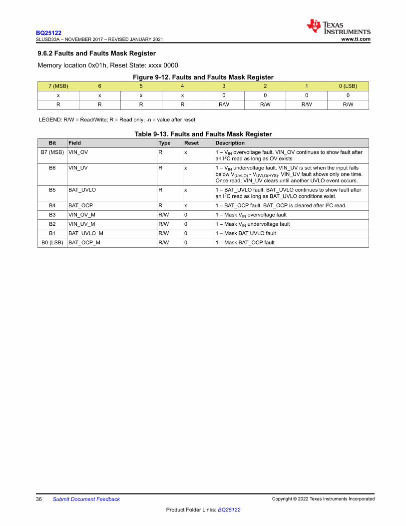
9.6.2 Faults and Faults Mask Register
Memory location 0x01h, Reset State: xxxx 0000
Figure 9-12. Faults and Faults Mask Register7 (MSB) 6 5 4 3 2 1 0 (LSB)
x x x x 0 0 0 0
R R R R R/W R/W R/W R/W
LEGEND: R/W = Read/Write; R = Read only; -n = value after reset
Table 9-13. Faults and Faults Mask RegisterBit Field Type Reset Description
B7 (MSB) VIN_OV R x 1 – VIN overvoltage fault. VIN_OV continues to show fault after an I2C read as long as OV exists
B6 VIN_UV R x 1 – VIN undervoltage fault. VIN_UV is set when the input falls below V(UVLO) - VUVLO(HYS). VIN_UV fault shows only one time. Once read, VIN_UV clears until another UVLO event occurs.
B5 BAT_UVLO R x 1 – BAT_UVLO fault. BAT_UVLO continues to show fault after an I2C read as long as BAT_UVLO conditions exist.
B4 BAT_OCP R x 1 – BAT_OCP fault. BAT_OCP is cleared after I2C read.
B3 VIN_OV_M R/W 0 1 – Mask VIN overvoltage fault
B2 VIN_UV_M R/W 0 1 – Mask VIN undervoltage fault
B1 BAT_UVLO_M R/W 0 1 – Mask BAT UVLO fault
B0 (LSB) BAT_OCP_M R/W 0 1 – Mask BAT_OCP fault
BQ25122SLUSD33A – NOVEMBER 2017 – REVISED JANUARY 2021 www.ti.com
36 Submit Document Feedback Copyright © 2022 Texas Instruments Incorporated
Product Folder Links: BQ25122
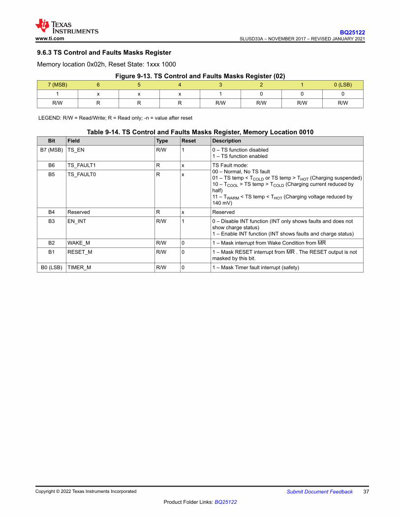
9.6.3 TS Control and Faults Masks Register
Memory location 0x02h, Reset State: 1xxx 1000
Figure 9-13. TS Control and Faults Masks Register (02)7 (MSB) 6 5 4 3 2 1 0 (LSB)
1 x x x 1 0 0 0
R/W R R R R/W R/W R/W R/W
LEGEND: R/W = Read/Write; R = Read only; -n = value after reset
Table 9-14. TS Control and Faults Masks Register, Memory Location 0010Bit Field Type Reset Description
B7 (MSB) TS_EN R/W 1 0 – TS function disabled1 – TS function enabled
B6 TS_FAULT1 R x TS Fault mode:00 – Normal, No TS fault01 – TS temp < TCOLD or TS temp > THOT (Charging suspended)10 – TCOOL > TS temp > TCOLD (Charging current reduced by half)11 – TWARM < TS temp < THOT (Charging voltage reduced by 140 mV)
B5 TS_FAULT0 R x
B4 Reserved R x Reserved
B3 EN_INT R/W 1 0 – Disable INT function (INT only shows faults and does not show charge status)1 – Enable INT function (INT shows faults and charge status)
B2 WAKE_M R/W 0 1 – Mask interrupt from Wake Condition from MR
B1 RESET_M R/W 0 1 – Mask RESET interrupt from MR . The RESET output is not masked by this bit.
B0 (LSB) TIMER_M R/W 0 1 – Mask Timer fault interrupt (safety)
www.ti.comBQ25122
SLUSD33A – NOVEMBER 2017 – REVISED JANUARY 2021
Copyright © 2022 Texas Instruments Incorporated Submit Document Feedback 37
Product Folder Links: BQ25122

9.6.4 Fast Charge Control Register
Memory location 0x03h, Reset State: 0001 1000
Figure 9-14. Fast Charge Control Register7 (MSB) 6 5 4 3 2 1 0 (LSB)
0 0 0 1 1 0 0 0
R/W R/W R/W R/W R/W R/W R/W R/W
LEGEND: R/W = Read/Write; R = Read only; -n = value after reset
Table 9-15. Fast Charge Control RegisterBit Field Type Reset Description
B7 (MSB) ICHRG_RANGE R/W 0 0 – To select charge range from 5 mA to 35 mA, ICHRG bits are 1-mA steps1 – To select charge range from 40 mA to 300 mA, ICHRG bits are 10-mA steps
B6 ICHRG_4 R/W 0 Charge current 16 mA or 160 mA
B5 ICHRG_3 R/W 0 Charge current 8 mA or 80 mA
B4 ICHRG_2 R/W 1 Charge current 4 mA or 40 mA
B3 ICHRG_1 R/W 1 Charge current 2 mA or 20 mA
B2 ICHRG_0 R/W 0 Charge current 1 mA or 10 mA
B1 CE R/W 0 0 – Charger enabled1 – Charger is disabled
B0 (LSB) HZ_MODE R/W 0 0 – Not high impedance mode1 – High impedance mode
ICHRG_RANGE and ICHRG bits are used to set the charge current. The ICHRG is calculated using the following equation: If ICHRG_RANGE is 0, then ICHRG = 5 mA + ICHRGCODE x 1 mA. If ICHRG_RANGE is 1, then ICHRG = 40 mA + ICHRGCODE x 10 mA. If a value greater than 35 mA (ICHRG_RANGE = 0) or 300 mA (ICHRG_RANGE = 1) is written, the setting goes to 35 mA or 300 mA respectively except if the ICHRG bits are all 1 (that is, 11111), then the externally programmed value is used. The PRETERM bits must also be set prior to writing all 1s to ensure the external ISET current is used as well as the proper termination and pre-charge values are used. For IPRETERM = 5%, set the IPRETERM bits to 000001, for IPRETERM = 10%, set the IPRETERM bits to 000010, for IPRETERM = 15%, set the IPRETERM bits to 000100, and for IPRETERM = 20%, set the iPRETERM bits to 001000. The default may be overridden by the external resistor on ISET.
BQ25122SLUSD33A – NOVEMBER 2017 – REVISED JANUARY 2021 www.ti.com
38 Submit Document Feedback Copyright © 2022 Texas Instruments Incorporated
Product Folder Links: BQ25122

9.6.5 Termination/Pre-Charge
Memory location 0x04h, Reset State: 0000 0010
Figure 9-15. Termination/Pre-Charge Register7 (MSB) 6 5 4 3 2 1 0 (LSB)
0 0 0 0 0 0 1 0
R/W R/W R/W R/W R/W R/W R/W R/W
LEGEND: R/W = Read/Write; R = Read only; -n = value after reset
Table 9-16. Termination/Pre-Charge RegisterBit Field Type Reset Description
B7 (MSB) IPRETERM_RANGE R/W 0 0 – To select termination range from 500 µA to 5 mA, IPRETERM bits are 500-µA steps1 – To select charge range from 6 mA to 37 mA, IPRETERM bits are 1-mA steps
B6 IPRETERM_4 R/W 0 Termination current 8 mA or 16 mA
B5 IPRETERM_3 R/W 0 Termination current 4 mA or 8 mA
B4 IPRETERM_2 R/W 0 Termination current 2 mA or 4 mA
B3 IPRETERM_1 R/W 0 Termination current 1 mA or 2 mA
B2 IPRETERM_0 R/W 0 Termination current 500 µA or 1 mA
B1 TE R/W 1 0 – Disable charge current termination1 – Enable charge current termination
B0 (LSB) R/W 0
IPRETERM_RANGE and IPRETERM bits are used to set the termination and pre-charge current. The ITERM is calculated using the following equation: If IPRETERM_RANGE is 0, then ITERM = 500 µA + ITERMCODE x 500 µA. If IPRETERM_RANGE is 1, then ITERM = 6 mA + ITERMCODE x 1 mA. If a value greater than 5 mA (IPRETERM_RANGE = 0) is written, the setting goes to 5 mA. Termination is disabled if any loop other than CC or DV in control, such as VINDPM, and TS/Cool. The default may be overridden by the external resistor on IPRETERM.
9.6.6 Battery Voltage Control Register
Memory location 0x05h, Reset State: 0111 1000
Figure 9-16. Battery Voltage Control Register7 (MSB) 6 5 4 3 2 1 0 (LSB)
0 1 1 1 1 0 0 0
R/W R/W R/W R/W R/W R/W R/W R/W
LEGEND: R/W = Read/Write; R = Read only; -n = value after reset
Table 9-17. Battery Voltage Control RegisterBit Field Type Reset Description
B7 (MSB) VBREG_6 R/W 0 Battery Regulation Voltage: 640 mV
B6 VBREG_5 R/W 1 Battery Regulation Voltage: 320 mV
B5 VBREG_4 R/W 1 Battery Regulation Voltage: 160 mV
B4 VBREG_3 R/W 1 Battery Regulation Voltage: 80 mV
B3 VBREG_2 R/W 1 Battery Regulation Voltage: 40 mV
B2 VBREG_1 R/W 0 Battery Regulation Voltage: 20 mV
B1 VBREG_0 R/W 0 Battery Regulation Voltage: 10 mV
B0 (LSB) R/W 0
www.ti.comBQ25122
SLUSD33A – NOVEMBER 2017 – REVISED JANUARY 2021
Copyright © 2022 Texas Instruments Incorporated Submit Document Feedback 39
Product Folder Links: BQ25122

Table 9-17. Battery Voltage Control Register (continued)Bit Field Type Reset Description
VBREG Bits: Use VBREG bits to set the battery regulation threshold. The VBATREG is calcuated using the following equation: VBATREG = 3.6 V + VBREGCODE x 10 mV. The charge voltage range is from 3.6 V to 4.65 V. If a value greater than 4.65 V is written, the setting goes to 4.65 V.
BQ25122SLUSD33A – NOVEMBER 2017 – REVISED JANUARY 2021 www.ti.com
40 Submit Document Feedback Copyright © 2022 Texas Instruments Incorporated
Product Folder Links: BQ25122

9.6.7 SYS VOUT Control Register
Memory location 0x06h, Reset State: 1000 0010
Figure 9-17. SYS VOUT Control Register7 (MSB) 6 5 4 3 2 1 0 (LSB)
1 0 0 0 0 0 1 0
R/W R/W R/W R/W R/W R/W R/W R/W
LEGEND: R/W = Read/Write; R = Read only; -n = value after reset
Table 9-18. SYS VOUT Control RegisterBit Field Type Reset Description
B7 (MSB) EN_SYS_OUT R/W 1 0 – Disable SW1 – Enable SW(When disabled, output is pulled low)
B6 SYS_SEL1 R/W 0 00 – 1.1 V and 1.2 V selection01 – 1.3 V through 2.8 V selection10 – 1.5V through 2.75 V selection11 – 1.8 V through 3.3 V selection
B5 SYS_SEL0 R/W 0
B4 SYS_VOUT_3 R/W 0 OUT Voltage: 800 mV step if SYS_SEL is 01 or 11
B3 SYS_VOUT_2 R/W 0 OUT Voltage: 400 mV step if SYS_SEL is 01 or 11
B2 SYS_VOUT_1 R/W 0 OUT Voltage: 200 mV step if SYS_SEL is 01 or 11
B1 SYS_VOUT_0 R/W 1 OUT Voltage: 100 mV step if SYS_SEL is 01 or 11
B0 (LSB) 0
SW_VOUT Bits: Use SYS_SEL and SYS_VOUT bits to set the output on SYS. The SYS voltage is calculated using the following equation:See table below for all VOUT values that can be programmed through SYS_SEL and SYS_VOUT.If SYS_SEL = 01, then SYS = 1.30 V + SYS_VOUTCODE x 100 mV.If SYS_SEL = 11, then SYS = 1.80 V + SYS_VOUTCODE x 100 mV.
Table 9-19. SYS_SEL CodesSYS_SEL SYS_VOUT TYP UNIT
00 0000 1.1 V
00 0001 1.2 V
00 0010 1.25 V
00 0011 1.333 V
00 0100 1.417 V
00 0101 1.5 V
00 0110 1.583 V
00 0111 1.667 V
00 1000 1.75 V
00 1001 1.833 V
00 1010 1.917 V
00 1011 2 V
00 1100 2.083 V
00 1101 2.167 V
00 1110 2.25 V
00 1111 2.333 V
01 0000 1.3 V
01 0001 1.4 V
01 0010 1.5 V
01 0011 1.6 V
www.ti.comBQ25122
SLUSD33A – NOVEMBER 2017 – REVISED JANUARY 2021
Copyright © 2022 Texas Instruments Incorporated Submit Document Feedback 41
Product Folder Links: BQ25122

Table 9-19. SYS_SEL Codes (continued)SYS_SEL SYS_VOUT TYP UNIT
01 0100 1.7 V
01 0101 1.8 V
01 0110 1.9 V
01 0111 2 V
01 1000 2.1 V
01 1001 2.2 V
01 1010 2.3 V
01 1011 2.4 V
01 1100 2.5 V
01 1101 2.6 V
01 1110 2.7 V
01 1111 2.8 V
10 0000 1.5 V
10 0001 1.583 V
10 0010 1.667 V
10 0011 1.75 V
10 0100 1.833 V
10 0101 1.917 V
10 0110 2 V
10 0111 2.083 V
10 1000 2.167 V
10 1001 2.25 V
10 1010 2.333 V
10 1011 2.417 V
10 1100 2.5 V
10 1101 2.583 V
10 1110 2.667 V
10 1111 2.75 V
11 0000 1.8 V
11 0001 1.9 V
11 0010 2 V
11 0011 2.1 V
11 0100 2.2 V
11 0101 2.3 V
11 0110 2.4 V
11 0111 2.5 V
11 1000 2.6 V
11 1001 2.7 V
11 1010 2.8 V
11 1011 2.9 V
11 1100 3 V
11 1101 3.1 V
11 1110 3.2 V
11 1111 3.3 V
BQ25122SLUSD33A – NOVEMBER 2017 – REVISED JANUARY 2021 www.ti.com
42 Submit Document Feedback Copyright © 2022 Texas Instruments Incorporated
Product Folder Links: BQ25122
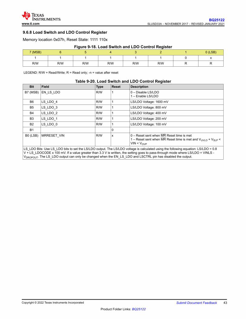
9.6.8 Load Switch and LDO Control Register
Memory location 0x07h, Reset State: 1111 110x
Figure 9-18. Load Switch and LDO Control Register7 (MSB) 6 5 4 3 2 1 0 (LSB)
1 1 1 1 1 1 0 x
R/W R/W R/W R/W R/W R/W R R
LEGEND: R/W = Read/Write; R = Read only; -n = value after reset
Table 9-20. Load Switch and LDO Control RegisterBit Field Type Reset Description
B7 (MSB) EN_LS_LDO R/W 1 0 – Disable LS/LDO1 – Enable LS/LDO
B6 LS_LDO_4 R/W 1 LS/LDO Voltage: 1600 mV
B5 LS_LDO_3 R/W 1 LS/LDO Voltage: 800 mV
B4 LS_LDO_2 R/W 1 LS/LDO Voltage: 400 mV
B3 LS_LDO_1 R/W 1 LS/LDO Voltage: 200 mV
B2 LS_LDO_0 R/W 1 LS/LDO Voltage: 100 mV
B1 0
B0 (LSB) MRRESET_VIN R/W x 0 – Reset sent when MR Reset time is met1 – Reset sent when MR Reset time is met and VUVLO + VSLP < VIN < VOVP
LS_LDO Bits: Use LS_LDO bits to set the LS/LDO output. The LS/LDO voltage is calculated using the following equation: LS/LDO = 0.8 V + LS_LDOCODE x 100 mV. If a value greater than 3.3 V is written, the setting goes to pass-through mode where LS/LDO = VINLS - VDROPOUT. The LS_LDO output can only be changed when the EN_LS_LDO and LSCTRL pin has disabled the output.
www.ti.comBQ25122
SLUSD33A – NOVEMBER 2017 – REVISED JANUARY 2021
Copyright © 2022 Texas Instruments Incorporated Submit Document Feedback 43
Product Folder Links: BQ25122

9.6.9 Push-Button Control Register
Memory location 0x08h, Reset State: 0110 00xx
Figure 9-19. Push-Button Control Register7 (MSB) 6 5 4 3 2 1 0 (LSB)
0 1 1 0 0 0 x x
R/W R/W R/W R/W R/W R/W R R
LEGEND: R/W = Read/Write; R = Read only; -n = value after reset
Table 9-21. Push-Button Control RegisterBit Field Type Reset Description
B7 (MSB) MRWAKE1 R/W 0 MR Timer adjustment for WAKE1:0 – 80 ms < MR1 – 600 ms < MR
B6 MRWAKE2 R/W 1 MR Timer adjustment for WAKE2:0 –1000 ms < MR1 – 1500 ms < MR
B5 MRREC R/W 1 0 – After Reset, device enters Ship mode1 – After Reset, device enters Hi-Z Mode
B4 MRRESET_1 R/W 0 MR Timer adjustment for reset:00 – 5 s ± 20%01 – 9 s ± 20%10 – 11 s ± 20%11 – 15 s ± 20%
B3 MRRESET_0 R/W 0
B2 PGB_MR R/W 0 0 – Output functions as PG1 – Output functions as voltage shifted push-button ( MR) input
B1 WAKE1 R x 1 – WAKE1 status. Indicates when the device meets the WAKE1 conditions, and is cleared after I2C read.
B0 (LSB) WAKE2 R x 1 – WAKE2 status. Indicates when the device meets the WAKE2 conditions, and is cleared after I2C read.
BQ25122SLUSD33A – NOVEMBER 2017 – REVISED JANUARY 2021 www.ti.com
44 Submit Document Feedback Copyright © 2022 Texas Instruments Incorporated
Product Folder Links: BQ25122
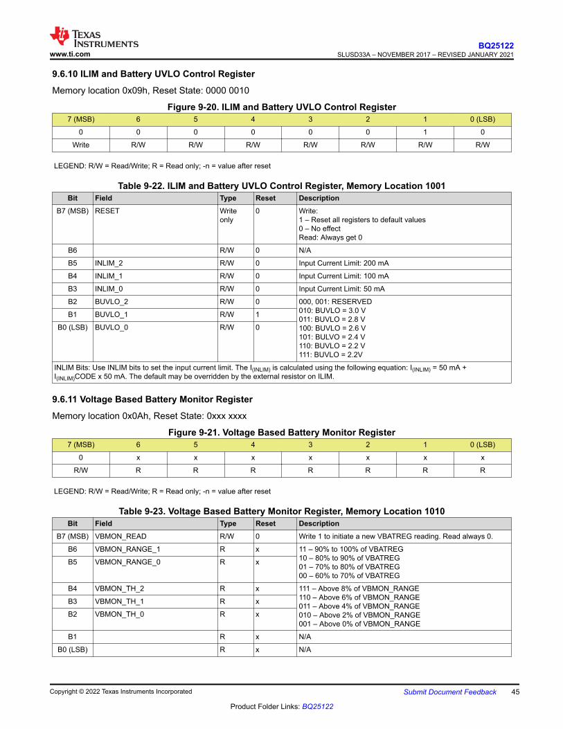
9.6.10 ILIM and Battery UVLO Control Register
Memory location 0x09h, Reset State: 0000 0010
Figure 9-20. ILIM and Battery UVLO Control Register7 (MSB) 6 5 4 3 2 1 0 (LSB)
0 0 0 0 0 0 1 0
Write R/W R/W R/W R/W R/W R/W R/W
LEGEND: R/W = Read/Write; R = Read only; -n = value after reset
Table 9-22. ILIM and Battery UVLO Control Register, Memory Location 1001Bit Field Type Reset Description
B7 (MSB) RESET Write only
0 Write:1 – Reset all registers to default values0 – No effectRead: Always get 0
B6 R/W 0 N/A
B5 INLIM_2 R/W 0 Input Current Limit: 200 mA
B4 INLIM_1 R/W 0 Input Current Limit: 100 mA
B3 INLIM_0 R/W 0 Input Current Limit: 50 mA
B2 BUVLO_2 R/W 0 000, 001: RESERVED010: BUVLO = 3.0 V011: BUVLO = 2.8 V100: BUVLO = 2.6 V101: BULVO = 2.4 V110: BUVLO = 2.2 V111: BUVLO = 2.2V
B1 BUVLO_1 R/W 1
B0 (LSB) BUVLO_0 R/W 0
INLIM Bits: Use INLIM bits to set the input current limit. The I(INLIM) is calculated using the following equation: I(INLIM) = 50 mA + I(INLIM)CODE x 50 mA. The default may be overridden by the external resistor on ILIM.
9.6.11 Voltage Based Battery Monitor Register
Memory location 0x0Ah, Reset State: 0xxx xxxx
Figure 9-21. Voltage Based Battery Monitor Register7 (MSB) 6 5 4 3 2 1 0 (LSB)
0 x x x x x x x
R/W R R R R R R R
LEGEND: R/W = Read/Write; R = Read only; -n = value after reset
Table 9-23. Voltage Based Battery Monitor Register, Memory Location 1010Bit Field Type Reset Description
B7 (MSB) VBMON_READ R/W 0 Write 1 to initiate a new VBATREG reading. Read always 0.
B6 VBMON_RANGE_1 R x 11 – 90% to 100% of VBATREG10 – 80% to 90% of VBATREG01 – 70% to 80% of VBATREG00 – 60% to 70% of VBATREG
B5 VBMON_RANGE_0 R x
B4 VBMON_TH_2 R x 111 – Above 8% of VBMON_RANGE110 – Above 6% of VBMON_RANGE011 – Above 4% of VBMON_RANGE010 – Above 2% of VBMON_RANGE001 – Above 0% of VBMON_RANGE
B3 VBMON_TH_1 R x
B2 VBMON_TH_0 R x
B1 R x N/A
B0 (LSB) R x N/A
www.ti.comBQ25122
SLUSD33A – NOVEMBER 2017 – REVISED JANUARY 2021
Copyright © 2022 Texas Instruments Incorporated Submit Document Feedback 45
Product Folder Links: BQ25122

Table 9-23. Voltage Based Battery Monitor Register, Memory Location 1010 (continued)Bit Field Type Reset Description
The VBMON registers are used to determine the battery voltage. Before entering a low power state, the device will determine the voltage level by starting at VBMON_RANGE 11 (90% to 100%), and if VBMON_TH of 000 is read, then it will move to VBMON_RANGE 10 (80% to 90%) and continue until a non 000 value of VBMON_TH is found. If this does not happen, then VBMON_RANGE and VBMON_TH will be written with 00 000. The VBMON_READ bit can be used to initiate a new reading by writing a 1 to it. Example: A reading of 10 011 indicated a VBAT voltage of between 84% and 86% of the VBATREG setting.
BQ25122SLUSD33A – NOVEMBER 2017 – REVISED JANUARY 2021 www.ti.com
46 Submit Document Feedback Copyright © 2022 Texas Instruments Incorporated
Product Folder Links: BQ25122

9.6.12 VIN_DPM and Timers Register
Memory location 0x0Bh, Reset State: 0100 0010
Figure 9-22. VIN_DPM and Timers Register7 (MSB) 6 5 4 3 2 1 0 (LSB)
0 1 0 0 0 0 1 0
R/W R/W R/W R/W R/W R/W R/W R/W
LEGEND: R/W = Read/Write; R = Read only; -n = value after reset
Table 9-24. VIN_DPM and Timers RegisterBit Field Type Reset Description
B7 (MSB) VINDPM_ON R/W 0 0 – Enable VINDPM1 – Disable VINDPM
B6 VINDPM_2 R/W 1 Input V(IN_DPM) voltage: 400 mV
B5 VINDPM_1 R/W 0 Input V(IN_DPM) voltage: 200 mV
B4 VINDPM_0 R/W 0 Input V(IN_DPM) voltage: 100 mV
B3 2XTMR_EN R/W 0 0 – Timer is not slowed at any time1 – Timer is slowed by 2x when in any control other than CC or CV
B2 TMR_1 R/W 0 Safety Timer Time Limit00 – 30 minute fast charge01 – 3 hour fast charge10 – 9 hour fast charge11 – Disable safety timers
B1 TMR_0 R/W 1
B0 (LSB) 0
The VINDPM threshold is set using the following equation: VINDPM = 4.2 + VINDPM_CODE x 100 mV
www.ti.comBQ25122
SLUSD33A – NOVEMBER 2017 – REVISED JANUARY 2021
Copyright © 2022 Texas Instruments Incorporated Submit Document Feedback 47
Product Folder Links: BQ25122

10 Application and ImplementationNote
Information in the following applications sections is not part of the TI component specification, and TI does not warrant its accuracy or completeness. TI’s customers are responsible for determining suitability of components for their purposes, as well as validating and testing their design implementation to confirm system functionality.
10.1 Application InformationA typical design is shown in Figure 10-1. This design uses the BQ25122 with external resistors for ILIM, IPRETERM, and ISET. These are not needed if these values are set with a host controller through I2C commands. This design also shows the TS resistors, which is also optional.
When powering up in default mode the battery voltage is the default for the part (4.2 V), the SYS output is the default (1.8 V). External resistors set the charge current to 40 mA, the termination current to 10% (4 mA), and the input current limit to 100 mA. If the I2C interface is used the part goes to the internal default settings until changed by the host.
10.2 Typical Application
GND
HOST
SDA
SCL
INT
SW
BAT
MR
BQ25122
MCU / SYSTEM
-+
NTCTS
LS / LDO <100mALoad
IN
SYS
RESET
LSCTRL
VINLS
Unregulated Load
PMIDPG
IPRETERM
ISET
ILIM
CD
IN
4.7 µF
`
2.2 µH
10 µF
1 µF
1 µF
14 k
14.3 k
499 4.99 k
4 k
1 µF
Figure 10-1. Typical Application Circuit
BQ25122SLUSD33A – NOVEMBER 2017 – REVISED JANUARY 2021 www.ti.com
48 Submit Document Feedback Copyright © 2022 Texas Instruments Incorporated
Product Folder Links: BQ25122

10.2.1 Design Requirements
This application is for a low power system that has varying loads from less than 10 mA up to 300 mA. It must work with a valid adaptor or USB power input. Below are some of the key components that are needed in normal operation. For this example, the fast charge current is 50 mA, input current limit is 400 mA and the pre-charge and termination current is 10% of the fast charge current.
• Supply voltage = 3.4 V to 20 V• Fast charge current is default to 10 mA with ISET pin shorted to ground. To program the fast charge current,
connect an external resistor from ISET to ground.• Input current limit is default to 100 mA with ILIM pin shorted to ground. To program the input current limit,
connect an external resistor from ILIM to ground.• Termination current threshold is default to 2 mA with IPRETERM pin shorted to ground. To program the input
current limit, connect an external resistor from IPRETERM to ground.• A 2.2-µH inductor is needed between SW pin and SYS pin for PWM output.• TS- Battery temperature sense needs a NTC connected on TS pin.
10.2.2 Detailed Design Procedure
See Figure 10-1 for an example of the application diagram.
10.2.2.1 Default Settings
• Connect ISET, ILIM and IPRETERM pins to ground to program fast charge current to 10mA, input current limit to 100mA and pre-charge/termination current to 2 mA.
• BAT_UVLO = 3 V• VSYS = 1.8 V• LS/LDO is LS• VBREG = 4.2 V• VIN_DPM is enabled and VIN_DPM Threshold = 4.6 V.• Safety Timer = 3 hr• If the function is not needed, connect TS to the center tab of the resistor divider between VIN and the ground.
(pull up resistor = 14 kΩ, pull down resistor = 14.3 kΩ)
10.2.2.2 Choose the Correct Inductance and Capacitance
Refer to the Section 9.3.21 section for the detailed procedure to determine the optimal inductance and capacitance for the buck output.
10.2.2.3 Calculations10.2.2.3.1 Program the Fast Charge Current (ISET)
RISET = KISET/ICHG (10)
KISET = 200 AΩ from the Section 8 table
RISET = 200 AΩ / 0.05A = 4 kΩ (11)
Select the closest standard value, which in this case is 4.99 kΩ. Connect this resistor between ISET pin and GND.
10.2.2.3.2 Program the Input Current Limit (ILIM)
RILIM = KILIM/II_MAX (12)
KILIM = 200 AΩ from the Section 8 table
RILIM = 200 AΩ / 0.4A = 500 Ω (13)
Select the closest standard value, which in this case is 499 Ω. Connect this resistor between ILIM pin and GND.
www.ti.comBQ25122
SLUSD33A – NOVEMBER 2017 – REVISED JANUARY 2021
Copyright © 2022 Texas Instruments Incorporated Submit Document Feedback 49
Product Folder Links: BQ25122

10.2.2.3.3 Program the Pre-charge/termination Threshold (IPRETERM)
According to Table 9-3, the RIPRETERM is 4990 Ω for 10% termination threshold. Therefore, connect a 4.99 kΩ resistor between IPRETERM pin and GND.
10.2.2.3.4 TS Resistors (TS)
The voltage at TS is monitored to determine that the battery is at a safe temperature during charging. This device uses JEITA temperature profile which has four temperature thresholds. Refer to Section 8 for the detailed thresholds number.
The TS circuit is shown in Figure 9-4. The resistor values can be calculated using Equation 1 and Equation 2.
BQ25122SLUSD33A – NOVEMBER 2017 – REVISED JANUARY 2021 www.ti.com
50 Submit Document Feedback Copyright © 2022 Texas Instruments Incorporated
Product Folder Links: BQ25122

10.2.3 Application Performance Curves10.2.3.1 Charger Curves
Time 100 s/divm
1 V
/div
5 V
/div
5 V
/div
5 V
/div
Figure 10-2. Battery Connected to V(BAT)
Time 4 ms/div
10 m
A/d
iv
500 m
V/d
iv
5 V
/div
5 V
/div
Figure 10-3. Power Supply Connected to VIN
Time 4 ms/div
500 m
V/d
iv
100 m
A/d
iv
2 V
/div
500 m
V/d
iv
Figure 10-4. Entering DPPM ModeTime 4 ms/div
10 m
A/d
iv
100 m
A/d
iv
2 V
/div
500 m
V/d
iv
Figure 10-5. Exiting DPPM Mode
Time 4 ms/div
20 m
A/d
iv
100 m
A/d
iv
2 V
/div
500 m
V/d
iv
Figure 10-6. Entering Battery Supplement ModeTime 4 ms/div
20 m
A/d
iv
100 m
A/d
iv
2 V
/div
500 m
V/d
iv
Figure 10-7. Exiting Battery Supplement Mode
www.ti.comBQ25122
SLUSD33A – NOVEMBER 2017 – REVISED JANUARY 2021
Copyright © 2022 Texas Instruments Incorporated Submit Document Feedback 51
Product Folder Links: BQ25122

Time 2 ms/div
10 m
A/d
iv
100 m
A/d
iv
2 V
/div
500 m
V/d
iv
Figure 10-8. Charger On/Off Using CD Time 4 ms/div
10 m
A/d
iv20 m
A/d
iv
2 V
/div
500 m
V/d
iv
Figure 10-9. OVP Fault
BQ25122SLUSD33A – NOVEMBER 2017 – REVISED JANUARY 2021 www.ti.com
52 Submit Document Feedback Copyright © 2022 Texas Instruments Incorporated
Product Folder Links: BQ25122
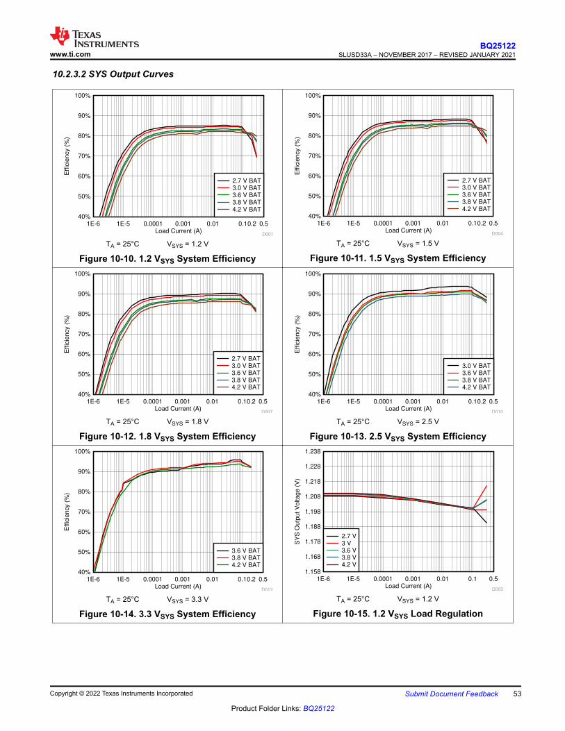
10.2.3.2 SYS Output Curves
Load Current (A)
Eff
icie
ncy (
%)
1E-6 1E-5 0.0001 0.001 0.01 0.10.2 0.540%
50%
60%
70%
80%
90%
100%
D001
2.7 V BAT3.0 V BAT3.6 V BAT3.8 V BAT4.2 V BAT
TA = 25°C VSYS = 1.2 V
Figure 10-10. 1.2 VSYS System Efficiency
Load Current (A)
Effic
iency (
%)
1E-6 1E-5 0.0001 0.001 0.01 0.10.2 0.540%
50%
60%
70%
80%
90%
100%
D004
2.7 V BAT3.0 V BAT3.6 V BAT3.8 V BAT4.2 V BAT
TA = 25°C VSYS = 1.5 V
Figure 10-11. 1.5 VSYS System Efficiency
Load Current (A)
Effic
iency (
%)
1E-6 1E-5 0.0001 0.001 0.01 0.10.2 0.540%
50%
60%
70%
80%
90%
100%
D007
2.7 V BAT3.0 V BAT3.6 V BAT3.8 V BAT4.2 V BAT
TA = 25°C VSYS = 1.8 V
Figure 10-12. 1.8 VSYS System Efficiency
Load Current (A)
Effic
iency (
%)
1E-6 1E-5 0.0001 0.001 0.01 0.10.2 0.540%
50%
60%
70%
80%
90%
100%
D010
3.0 V BAT3.6 V BAT3.8 V BAT4.2 V BAT
TA = 25°C VSYS = 2.5 V
Figure 10-13. 2.5 VSYS System Efficiency
Load Current (A)
Effic
iency (
%)
1E-6 1E-5 0.0001 0.001 0.01 0.10.2 0.540%
50%
60%
70%
80%
90%
100%
D013
3.6 V BAT3.8 V BAT4.2 V BAT
TA = 25°C VSYS = 3.3 V
Figure 10-14. 3.3 VSYS System Efficiency
Load Current (A)
SY
S O
utp
ut
Vo
ltag
e (
V)
1E-6 1E-5 0.0001 0.001 0.01 0.1 0.51.158
1.168
1.178
1.188
1.198
1.208
1.218
1.228
1.238
D003
2.7 V3 V3.6 V3.8 V4.2 V
TA = 25°C VSYS = 1.2 V
Figure 10-15. 1.2 VSYS Load Regulation
www.ti.comBQ25122
SLUSD33A – NOVEMBER 2017 – REVISED JANUARY 2021
Copyright © 2022 Texas Instruments Incorporated Submit Document Feedback 53
Product Folder Links: BQ25122
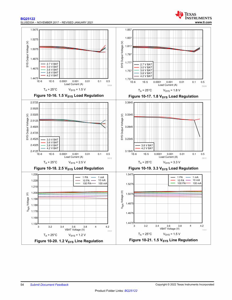
Load Current (A)
SY
S O
utp
ut V
oltage (
V)
1E-6 1E-5 0.0001 0.001 0.01 0.1 0.51.4475
1.4675
1.4875
1.5075
1.5275
1.5475
D006
2.7 V BAT3.0 V BAT3.6 V BAT3.8 V BAT4.2 V BAT
TA = 25°C VSYS = 1.5 V
Figure 10-16. 1.5 VSYS Load Regulation
Load Current (A)
SY
S O
utp
ut V
oltage (
V)
1E-6 1E-5 0.0001 0.001 0.01 0.1 0.51.737
1.757
1.777
1.797
1.817
1.837
1.857
D009
2.7 V BAT3.0 V BAT3.6 V BAT3.8 V BAT4.2 V BAT
TA = 25°C VSYS = 1.8 V
Figure 10-17. 1.8 VSYS Load Regulation
Load Current (A)
SY
S O
utp
ut
Voltage (
V)
1E-6 1E-5 0.0001 0.001 0.01 0.1 0.52.4125
2.4325
2.4525
2.4725
2.4925
2.5125
2.5325
2.5525
2.5725
D012
3.0 V BAT3.6 V BAT3.8 V BAT4.2 V BAT
TA = 25°C VSYS = 2.5 V
Figure 10-18. 2.5 VSYS Load Regulation
Load Current (A)
SY
S O
utp
ut
Voltage (
V)
1E-6 1E-5 0.0001 0.001 0.01 0.1 0.53.1845
3.2345
3.2845
3.3345
3.3845
D015
3.8 V BAT4.2 V BAT
TA = 25°C VSYS = 3.3 V
Figure 10-19. 3.3 VSYS Load Regulation
VBAT Voltage (V)
Vsys V
olta
ge
(V)
3 3.2 3.4 3.6 3.8 41.158
1.168
1.178
1.188
1.198
1.208
1.218
1.228
1.238
D002
1 PA
10 PA100 PA
1 mA10 mA
100 mA
4.2
TA = 25°C VSYS = 1.2 V
Figure 10-20. 1.2 VSYS Line Regulation
VBAT Voltage (V)
Vsys V
olta
ge
(V
)
3 3.2 3.4 3.6 3.8 41.4475
1.4675
1.4875
1.5075
1.5275
1.5475
D005
1 PA
10 PA100 PA
1 mA10 mA
100 mA
4.2
TA = 25°C VSYS = 1.5 V
Figure 10-21. 1.5 VSYS Line Regulation
BQ25122SLUSD33A – NOVEMBER 2017 – REVISED JANUARY 2021 www.ti.com
54 Submit Document Feedback Copyright © 2022 Texas Instruments Incorporated
Product Folder Links: BQ25122

VBAT Voltage (V)
Vsys V
ota
ge
(V
)
3 3.2 3.4 3.6 3.8 41.737
1.757
1.777
1.797
1.817
1.837
1.857
D008
1 PA10 PA
100 PA1 mA
10 mA100 mA
300ma
4.2
TA = 25°C VSYS = 1.8 V
Figure 10-22. 1.8 VSYS Line Regulation
VBAT Voltage (V)
V
sys V
olta
ge
(V
)
3 3.2 3.4 3.6 3.8 4
2.4125
2.4325
2.4525
2.4725
2.4925
2.5125
2.5325
2.5525
2.5725
D011
1 PA
10 PA100 PA
1 mA10 mA
100 mA
4.2
TA = 25°C VSYS = 2.1 V
Figure 10-23. 2.1 VSYS Line Regulation
VBAT Voltage (V)
V
sys V
ota
ge(V
)
3.8 43.1845
3.2345
3.2845
3.3345
3.3845
D014
1 PA
10 PA100 PA
1 mA10 mA
100 mA
4.2
TA = 25°C VSYS = 3.3 V
Figure 10-24. 3.3 VSYS Line Regulation
Load Current (mA)
Fre
quency,
FS
W (
kH
z)
0 50 100 150 200 250 3000
200
400
600
800
1000
1200
1400
D023
5 V VBAT
4.2 V VBAT
3.6 V VBAT
3 V VBAT
2.5 V VBAT
Figure 10-25. 1.8 VSYS Switching Frequency vs Load Current
Time 40 s/divm
500 m
A/d
iv
10 m
A/d
iv
2 V
/div5
V/d
iv
SW
ILOAD = 10 µA
Figure 10-26. Light Load Operation Showing SW
Time 40 s/divm
500 m
A/d
iv
10 m
A/d
iv
2 V
/div5
V/d
iv
SW
ILOAD = 100 mA
Figure 10-27. Light Load Operation Showing SW
www.ti.comBQ25122
SLUSD33A – NOVEMBER 2017 – REVISED JANUARY 2021
Copyright © 2022 Texas Instruments Incorporated Submit Document Feedback 55
Product Folder Links: BQ25122

Time 40 s/divm
500 m
A/d
iv
10 m
A/d
iv
2 V
/div5
V/d
iv
SW
ILOAD = 1 mA
Figure 10-28. Light Load Operation Showing SW
Time 2 s/divm
500 m
A/d
iv
10 m
A/d
iv
2 V
/div5
V/d
iv
SW
ILOAD = 10 mA
Figure 10-29. Light Load Operation Showing SW
Time 400 ns/div
500 m
A/d
iv
100 m
A/d
iv
2 V
/div5
V/d
iv
SW
ILOAD = 100 mA
Figure 10-30. Light Load Operation Showing SW
Time 400 ns/div
500 m
A/d
iv
200 m
A/d
iv
2 V
/div5
V/d
iv
SW
ILOAD = 200 mA
Figure 10-31. Light Load Operation Showing SW
Time 400 ns/div
500 m
A/d
iv
200 m
A/d
iv
2 V
/div5
V/d
iv
SW
ILOAD = 300 mA
Figure 10-32. Light Load Operation Showing SW
Time 4 s/divm
500 m
A/d
iv
50 m
V/d
iv
50 m
V/d
iv
5 V
/div
SW
VSYS = 1.2 V
Figure 10-33. 1.2 VSYS Load Transient, 0 to 50 mA
BQ25122SLUSD33A – NOVEMBER 2017 – REVISED JANUARY 2021 www.ti.com
56 Submit Document Feedback Copyright © 2022 Texas Instruments Incorporated
Product Folder Links: BQ25122

Time 4 s/divm
500 m
A/d
iv
50 m
V/d
iv
50 m
V/d
iv
5 V
/div
SW
VSYS = 1.8 V
Figure 10-34. 1.8 VSYS Load Transient, 0 to 50 mA
Time 4 s/divm
500 m
A/d
iv
50 m
V/d
iv
50 m
V/d
iv
5 V
/div
SW
VSYS = 2.1 V
Figure 10-35. 2.1 VSYS Load Transient, 0 to 50 mA
Time 4 s/divm
500 m
A/d
iv
50 m
V/d
iv
50 m
V/d
iv
5 V
/div
SW
VSYS = 2.5 V
Figure 10-36. 2.5 VSYS Load Transient, 0 to 50 mA
Time 4 s/divm
500 m
A/d
iv
50 m
V/d
iv
50 m
V/d
iv
5 V
/div
SW
VSYS = 3.3 V
Figure 10-37. 3.3 VSYS Load Transient, 0 to 50 mA
Time 4 s/divm
500 m
A/d
iv
200 m
V/d
iv 50 m
V/d
iv
5 V
/div
SW
VSYS = 1.2 V
Figure 10-38. 1.2 VSYS Load Transient, 0 to 200 mA
Time 4 s/divm
500 m
A/d
iv
200 m
V/d
iv 50 m
V/d
iv
5 V
/div
SW
VSYS = 1.8 V
Figure 10-39. 1.8 VSYS Load Transient, 0 to 200 mA
www.ti.comBQ25122
SLUSD33A – NOVEMBER 2017 – REVISED JANUARY 2021
Copyright © 2022 Texas Instruments Incorporated Submit Document Feedback 57
Product Folder Links: BQ25122

Time 4 s/divm
500 m
A/d
iv
200 m
V/d
iv 50 m
V/d
iv
5 V
/div
SW
VSYS = 2.1 V
Figure 10-40. 2.1 VSYS Load Transient, 0 to 200 mA
Time 4 s/divm
500 m
A/d
iv
200 m
V/d
iv 50 m
V/d
iv
5 V
/div
SW
VSYS = 2.5 V
Figure 10-41. 2.5 VSYS Load Transient, 0 to 200 mA
Time 4 s/divm
500 m
A/d
iv
200 m
V/d
iv 50 m
V/d
iv
5 V
/div
SW
VSYS = 3.3 V
Figure 10-42. 3.3 VSYS Load Transient, 0 to 200 mA
Time 1 ms/div
1 V
/div
5 V
/div
2 V
/div
Figure 10-43. Startup Showing SS on SYS in PWM Mode
Time 20 ms/div
500 m
A/d
iv
5 V
/div
2 V
/div
2 V
/div
Figure 10-44. Short Circuit and Recovery for SYS
BQ25122SLUSD33A – NOVEMBER 2017 – REVISED JANUARY 2021 www.ti.com
58 Submit Document Feedback Copyright © 2022 Texas Instruments Incorporated
Product Folder Links: BQ25122

10.2.3.3 Load Switch and LDO Curves
Time 20 ms/div
50 m
A/d
iv
2 V
/div
2 V
/div
Figure 10-45. Short Circuit and Recovery for LSTime 400 s/divm
20 m
A/d
iv
2 V
/div
2 V
/div
Figure 10-46. Startup Showing SS on LS/LDO Output
Time 4 s/divm
50 m
V/d
iv
5 V
/div
20 m
V/d
iv
VSLSDO = 0.8 V
Figure 10-47. 0.8 VLSLDO Load Transient, 0 to 10 mA
Time 4 s/divm
50 m
V/d
iv
5 V
/div
20 m
V/d
iv
VSLSDO = 1.2 V
Figure 10-48. 1.2 VLSLDO Load Transient, 0 to 10 mA
Time 4 s/divm
50 m
V/d
iv
5 V
/div
20 m
V/d
iv
VSLSDO = 1.8 V
Figure 10-49. 1.8 VLSLDO Load Transient, 0 to 10 mA
Time 4 s/divm
50 m
V/d
iv
5 V
/div
20 m
V/d
iv
VSLSDO = 2.5 V
Figure 10-50. 2.5 VLSLDO Load Transient, 0 to 10 mA
www.ti.comBQ25122
SLUSD33A – NOVEMBER 2017 – REVISED JANUARY 2021
Copyright © 2022 Texas Instruments Incorporated Submit Document Feedback 59
Product Folder Links: BQ25122
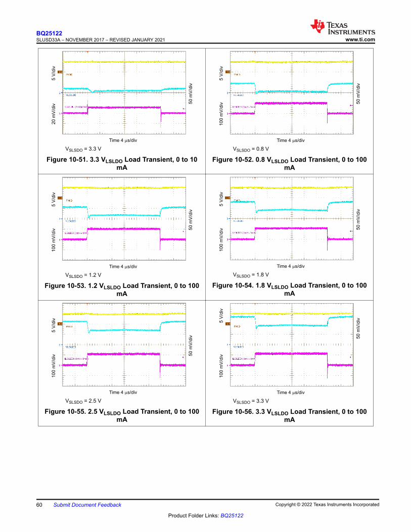
Time 4 s/divm
50 m
V/d
iv
5 V
/div
20 m
V/d
iv
VSLSDO = 3.3 V
Figure 10-51. 3.3 VLSLDO Load Transient, 0 to 10 mA
Time 4 s/divm
50 m
V/d
iv
5 V
/div
100 m
V/d
iv
VSLSDO = 0.8 V
Figure 10-52. 0.8 VLSLDO Load Transient, 0 to 100 mA
Time 4 s/divm
50 m
V/d
iv
5 V
/div
100 m
V/d
iv
VSLSDO = 1.2 V
Figure 10-53. 1.2 VLSLDO Load Transient, 0 to 100 mA
Time 4 s/divm
50 m
V/d
iv
5 V
/div
100 m
V/d
iv
VSLSDO = 1.8 V
Figure 10-54. 1.8 VLSLDO Load Transient, 0 to 100 mA
Time 4 s/divm
50 m
V/d
iv
5 V
/div
100 m
V/d
iv
VSLSDO = 2.5 V
Figure 10-55. 2.5 VLSLDO Load Transient, 0 to 100 mA
Time 4 s/divm
50 m
V/d
iv5 V
/div
100 m
V/d
iv
VSLSDO = 3.3 V
Figure 10-56. 3.3 VLSLDO Load Transient, 0 to 100 mA
BQ25122SLUSD33A – NOVEMBER 2017 – REVISED JANUARY 2021 www.ti.com
60 Submit Document Feedback Copyright © 2022 Texas Instruments Incorporated
Product Folder Links: BQ25122

10.2.3.4 LS/LDO Output Curves
Time 400 s/divm
20 m
A/d
iv
2 V
/div
2 V
/div
Figure 10-57. Startup Showing SS on LS/LDO in LDO Mode
Time 20 ms/div
200 m
A/d
iv
2 V
/div
2 V
/div
Figure 10-58. Short Circuit and Recovery for LDO
www.ti.comBQ25122
SLUSD33A – NOVEMBER 2017 – REVISED JANUARY 2021
Copyright © 2022 Texas Instruments Incorporated Submit Document Feedback 61
Product Folder Links: BQ25122
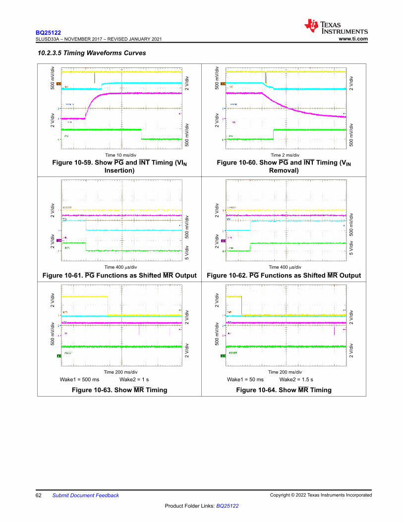
10.2.3.5 Timing Waveforms Curves
Time 10 ms/div
500 m
V/d
iv
500 m
V/d
iv2 V
/div
2 V
/div
Figure 10-59. Show PG and INT Timing (VIN Insertion)
Time 2 ms/div
500 m
V/d
iv
500 m
V/d
iv2 V
/div
2 V
/div
Figure 10-60. Show PG and INT Timing (VIN Removal)
Time 400 s/divm
500 m
V/d
iv2 V
/div
2 V
/div
5 V
/div
Figure 10-61. PG Functions as Shifted MR OutputTime 400 s/divm
500 m
V/d
iv2 V
/div
2 V
/div
5 V
/div
Figure 10-62. PG Functions as Shifted MR Output
Time 200 ms/div
2 V
/div
2 V
/div
500 m
V/d
iv
2 V
/div
Wake1 = 500 ms Wake2 = 1 s
Figure 10-63. Show MR Timing
Time 200 ms/div
2 V
/div
2 V
/div
500 m
V/d
iv
2 V
/div
Wake1 = 50 ms Wake2 = 1.5 s
Figure 10-64. Show MR Timing
BQ25122SLUSD33A – NOVEMBER 2017 – REVISED JANUARY 2021 www.ti.com
62 Submit Document Feedback Copyright © 2022 Texas Instruments Incorporated
Product Folder Links: BQ25122

Time 1 s/div
2 V
/div
2 V
/div
500 m
V/d
iv
2 V
/div
RESET = 4 s
Figure 10-65. RESET Timing
Time 1 s/div
2 V
/div
2 V
/div
500 m
V/d
iv
2 V
/div
RESET = 8 s
Figure 10-66. RESET Timing
Time 2 s/div
2 V
/div
2 V
/div
500 m
V/d
iv
2 V
/div
RESET = 14 s
Figure 10-67. RESET Timing
Time 2 s/div
2 V
/div
2 V
/div
500 m
V/d
iv
2 V
/div
Figure 10-68. RESET Timing and Enter Ship Mode
11 Power Supply RecommendationsIt is recommended to use a power supply that is capable of delivering 5 V at the input current limit set by the BQ25122.
www.ti.comBQ25122
SLUSD33A – NOVEMBER 2017 – REVISED JANUARY 2021
Copyright © 2022 Texas Instruments Incorporated Submit Document Feedback 63
Product Folder Links: BQ25122

12 Layout12.1 Layout Guidelines• Keep the core components of the system close to each other and the device.• Keep the PMID, IN, and SYS caps as close to their respective pins as possible. Place the bypass caps for
PMID, SYS, and LSLDO close to the pins.• Place the GNDs of the PMID and IN caps close to each other.• Do not route so the power planes are interrupted.
12.2 Layout Example
Figure 12-1. BQ25122 Layout
BQ25122SLUSD33A – NOVEMBER 2017 – REVISED JANUARY 2021 www.ti.com
64 Submit Document Feedback Copyright © 2022 Texas Instruments Incorporated
Product Folder Links: BQ25122
13 Device and Documentation Support13.1 Device Support13.1.1 Third-Party Products Disclaimer
TI'S PUBLICATION OF INFORMATION REGARDING THIRD-PARTY PRODUCTS OR SERVICES DOES NOT CONSTITUTE AN ENDORSEMENT REGARDING THE SUITABILITY OF SUCH PRODUCTS OR SERVICES OR A WARRANTY, REPRESENTATION OR ENDORSEMENT OF SUCH PRODUCTS OR SERVICES, EITHER ALONE OR IN COMBINATION WITH ANY TI PRODUCT OR SERVICE.
13.2 Documentation Support13.2.1 Related Documentation
For related documentation see the following:• bq25120AEVM and bq25122EVM Evaluation Modules User's Guide
13.3 Receiving Notification of Documentation UpdatesTo receive notification of documentation updates, navigate to the device product folder on ti.com. Click on Subscribe to updates to register and receive a weekly digest of any product information that has changed. For change details, review the revision history included in any revised document.
13.4 Support ResourcesTI E2E™ support forums are an engineer's go-to source for fast, verified answers and design help — straight from the experts. Search existing answers or ask your own question to get the quick design help you need.
Linked content is provided "AS IS" by the respective contributors. They do not constitute TI specifications and do not necessarily reflect TI's views; see TI's Terms of Use.
13.5 TrademarksTI E2E™ is a trademark of Texas Instruments.All trademarks are the property of their respective owners.13.6 Electrostatic Discharge Caution
This integrated circuit can be damaged by ESD. Texas Instruments recommends that all integrated circuits be handled with appropriate precautions. Failure to observe proper handling and installation procedures can cause damage.ESD damage can range from subtle performance degradation to complete device failure. Precision integrated circuits may be more susceptible to damage because very small parametric changes could cause the device not to meet its published specifications.
13.7 GlossaryTI Glossary This glossary lists and explains terms, acronyms, and definitions.
14 Mechanical, Packaging, and Orderable InformationThe following pages include mechanical, packaging, and orderable information. This information is the most current data available for the designated devices. This data is subject to change without notice and revision of this document. For browser-based versions of this data sheet, refer to the left-hand navigation.
www.ti.comBQ25122
SLUSD33A – NOVEMBER 2017 – REVISED JANUARY 2021
Copyright © 2022 Texas Instruments Incorporated Submit Document Feedback 65
Product Folder Links: BQ25122

PACKAGE OPTION ADDENDUM
www.ti.com 10-Dec-2020
Addendum-Page 1
PACKAGING INFORMATION
Orderable Device Status(1)
Package Type PackageDrawing
Pins PackageQty
Eco Plan(2)
Lead finish/Ball material
(6)
MSL Peak Temp(3)
Op Temp (°C) Device Marking(4/5)
Samples
BQ25122YFPR ACTIVE DSBGA YFP 25 3000 RoHS & Green SNAGCU Level-1-260C-UNLIM -40 to 85 BQ25122
BQ25122YFPT ACTIVE DSBGA YFP 25 250 RoHS & Green SNAGCU Level-1-260C-UNLIM -40 to 85 BQ25122
(1) The marketing status values are defined as follows:ACTIVE: Product device recommended for new designs.LIFEBUY: TI has announced that the device will be discontinued, and a lifetime-buy period is in effect.NRND: Not recommended for new designs. Device is in production to support existing customers, but TI does not recommend using this part in a new design.PREVIEW: Device has been announced but is not in production. Samples may or may not be available.OBSOLETE: TI has discontinued the production of the device.
(2) RoHS: TI defines "RoHS" to mean semiconductor products that are compliant with the current EU RoHS requirements for all 10 RoHS substances, including the requirement that RoHS substancedo not exceed 0.1% by weight in homogeneous materials. Where designed to be soldered at high temperatures, "RoHS" products are suitable for use in specified lead-free processes. TI mayreference these types of products as "Pb-Free".RoHS Exempt: TI defines "RoHS Exempt" to mean products that contain lead but are compliant with EU RoHS pursuant to a specific EU RoHS exemption.Green: TI defines "Green" to mean the content of Chlorine (Cl) and Bromine (Br) based flame retardants meet JS709B low halogen requirements of <=1000ppm threshold. Antimony trioxide basedflame retardants must also meet the <=1000ppm threshold requirement.
(3) MSL, Peak Temp. - The Moisture Sensitivity Level rating according to the JEDEC industry standard classifications, and peak solder temperature.
(4) There may be additional marking, which relates to the logo, the lot trace code information, or the environmental category on the device.
(5) Multiple Device Markings will be inside parentheses. Only one Device Marking contained in parentheses and separated by a "~" will appear on a device. If a line is indented then it is a continuationof the previous line and the two combined represent the entire Device Marking for that device.
(6) Lead finish/Ball material - Orderable Devices may have multiple material finish options. Finish options are separated by a vertical ruled line. Lead finish/Ball material values may wrap to twolines if the finish value exceeds the maximum column width.
Important Information and Disclaimer:The information provided on this page represents TI's knowledge and belief as of the date that it is provided. TI bases its knowledge and belief on informationprovided by third parties, and makes no representation or warranty as to the accuracy of such information. Efforts are underway to better integrate information from third parties. TI has taken andcontinues to take reasonable steps to provide representative and accurate information but may not have conducted destructive testing or chemical analysis on incoming materials and chemicals.TI and TI suppliers consider certain information to be proprietary, and thus CAS numbers and other limited information may not be available for release.
In no event shall TI's liability arising out of such information exceed the total purchase price of the TI part(s) at issue in this document sold by TI to Customer on an annual basis.

PACKAGE OPTION ADDENDUM
www.ti.com 10-Dec-2020
Addendum-Page 2

TAPE AND REEL INFORMATION
*All dimensions are nominal
Device PackageType
PackageDrawing
Pins SPQ ReelDiameter
(mm)
ReelWidth
W1 (mm)
A0(mm)
B0(mm)
K0(mm)
P1(mm)
W(mm)
Pin1Quadrant
BQ25122YFPR DSBGA YFP 25 3000 180.0 8.4 2.65 2.65 0.69 4.0 8.0 Q1
BQ25122YFPT DSBGA YFP 25 250 180.0 8.4 2.65 2.65 0.69 4.0 8.0 Q1
PACKAGE MATERIALS INFORMATION
www.ti.com 20-Aug-2020
Pack Materials-Page 1
*All dimensions are nominal
Device Package Type Package Drawing Pins SPQ Length (mm) Width (mm) Height (mm)
BQ25122YFPR DSBGA YFP 25 3000 182.0 182.0 20.0
BQ25122YFPT DSBGA YFP 25 250 182.0 182.0 20.0
PACKAGE MATERIALS INFORMATION
www.ti.com 20-Aug-2020
Pack Materials-Page 2

www.ti.com
PACKAGE OUTLINE
0.5 MAX
0.190.13
1.6TYP
0.4 TYP
0.4 TYP25X 0.25
0.21
0.300.25
1.6 TYP
E
D
4225306/A 09/2019
DSBGA - 0.5 mm max heightYFP0025DIE SIZE BALL GRID ARRAY
NOTES: 1. All linear dimensions are in millimeters. Any dimensions in parenthesis are for reference only. Dimensioning and tolerancing per ASME Y14.5M.2. This drawing is subject to change without notice.
BALL A1CORNER
SEATING PLANE
0.05 C
A
1 2
0.015 C A B
SYMM
SYMM
B
C
D
3 4 5
E
SCALE 8.000
AB
C
D: Max =
E: Max =
2.56 mm, Min =
2.498 mm, Min =
2.5 mm
2.438 mm

www.ti.com
EXAMPLE BOARD LAYOUT
0.05 MIN0.05 MAX
25X ( 0.23)
(0.4) TYP
(0.4) TYP
( 0.23)SOLDER MASKOPENING
( 0.23)METAL
4225306/A 09/2019
DSBGA - 0.5 mm max heightYFP0025DIE SIZE BALL GRID ARRAY
NOTES: (continued) 3. Final dimensions may vary due to manufacturing tolerance considerations and also routing constraints. See Texas Instruments Literature No. SNVA009 (www.ti.com/lit/snva009).
SOLDER MASK DETAILSNOT TO SCALE
SYMM
SYMM
C
1 2
A
B
D
LAND PATTERN EXAMPLEEXPOSED METAL SHOWN
SCALE: 40X
E
3 4 5
NON-SOLDER MASKDEFINED
(PREFERRED)
EXPOSEDMETAL
SOLDER MASKOPENING
SOLDER MASKDEFINED
METAL UNDERSOLDER MASK
EXPOSEDMETAL
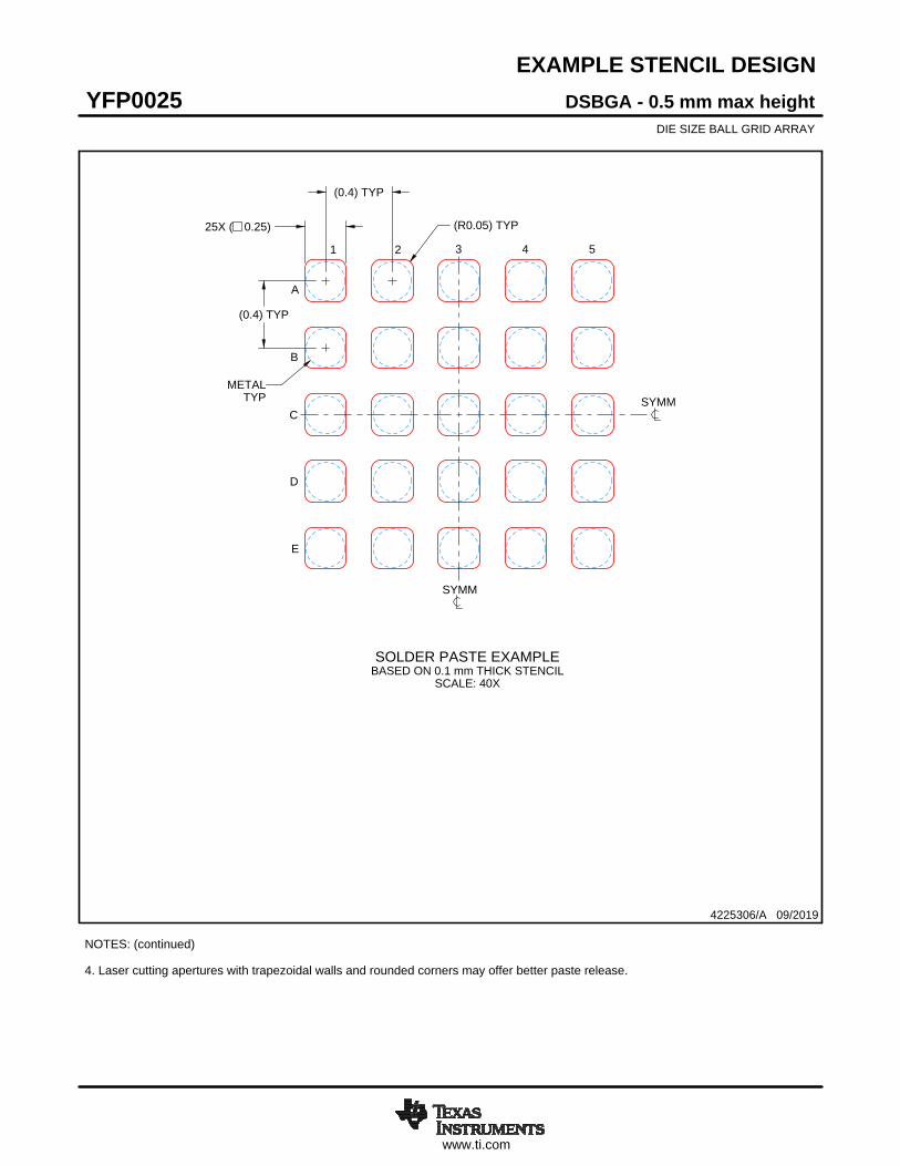
www.ti.com
EXAMPLE STENCIL DESIGN
(0.4) TYP
(0.4) TYP
25X ( 0.25) (R0.05) TYP
4225306/A 09/2019
DSBGA - 0.5 mm max heightYFP0025DIE SIZE BALL GRID ARRAY
NOTES: (continued) 4. Laser cutting apertures with trapezoidal walls and rounded corners may offer better paste release.
SYMM
SYMM
SOLDER PASTE EXAMPLEBASED ON 0.1 mm THICK STENCIL
SCALE: 40X
METALTYP
C
1 2
A
B
D
E
3 4 5

IMPORTANT NOTICE AND DISCLAIMERTI PROVIDES TECHNICAL AND RELIABILITY DATA (INCLUDING DATA SHEETS), DESIGN RESOURCES (INCLUDING REFERENCE DESIGNS), APPLICATION OR OTHER DESIGN ADVICE, WEB TOOLS, SAFETY INFORMATION, AND OTHER RESOURCES “AS IS” AND WITH ALL FAULTS, AND DISCLAIMS ALL WARRANTIES, EXPRESS AND IMPLIED, INCLUDING WITHOUT LIMITATION ANY IMPLIED WARRANTIES OF MERCHANTABILITY, FITNESS FOR A PARTICULAR PURPOSE OR NON-INFRINGEMENT OF THIRD PARTY INTELLECTUAL PROPERTY RIGHTS.These resources are intended for skilled developers designing with TI products. You are solely responsible for (1) selecting the appropriate TI products for your application, (2) designing, validating and testing your application, and (3) ensuring your application meets applicable standards, and any other safety, security, regulatory or other requirements.These resources are subject to change without notice. TI grants you permission to use these resources only for development of an application that uses the TI products described in the resource. Other reproduction and display of these resources is prohibited. No license is granted to any other TI intellectual property right or to any third party intellectual property right. TI disclaims responsibility for, and you will fully indemnify TI and its representatives against, any claims, damages, costs, losses, and liabilities arising out of your use of these resources.TI’s products are provided subject to TI’s Terms of Sale or other applicable terms available either on ti.com or provided in conjunction with such TI products. TI’s provision of these resources does not expand or otherwise alter TI’s applicable warranties or warranty disclaimers for TI products.TI objects to and rejects any additional or different terms you may have proposed. IMPORTANT NOTICE
Mailing Address: Texas Instruments, Post Office Box 655303, Dallas, Texas 75265Copyright © 2022, Texas Instruments Incorporated