breaking the buildup-time limit of sensitivity in ...ece-research.unm.edu/hayat/oe_2015.pdf ·...
TRANSCRIPT
Breaking the buildup-time limit of sensitivity in avalanche photodiodes by dynamic biasing Majeed M. Hayat,1,2,* Payman Zarkesh-Ha,1,2 Georges El-Howayek,1,3 Robert
Efroymson,2 and Joe C. Campbell4 1The Center for High Technology Materials and the Department of Electrical & Computer Engineering, University of
New Mexico, 1313 Goddard Street SE, Albuquerque, New Mexico 87106-4343, USA 2 Dynamic Photonics Inc., 1155 University Blvd NE, Albuquerque, New Mexico 87106, USA
3Department of Electrical and Computer Engineering, Valparaiso University, Valparaiso, Indiana 46383-6493, USA 4Department of Electrical and Computer Engineering, University of Virginia, PO Box 400743, Charlottesville,
Virginia 22904-4743, USA *[email protected]
Abstract: Avalanche photodiodes (APDs) are the preferred photodetectors for direct-detection, high data-rate long-haul optical telecommunications. APDs can detect low-level optical signals due to their internal amplification of the photon-generated electrical current, which is attributable to the avalanche of electron and hole impact ionizations. Despite recent advances in APDs aimed at reducing the average avalanche-buildup time, which causes intersymbol interference and compromises receiver sensitivity at high data rates, operable speeds of commercially available APDs have been limited to 10Gbps. We report the first demonstration of a dynamically biased APD that breaks the traditional sensitivity-versus-speed limit by employing a data-synchronous sinusoidal reverse-bias that drastically suppresses the average avalanche-buildup time. Compared with traditional DC biasing, the sensitivity of germanium APDs at 3Gbps is improved by 4.3 dB, which is equivalent to a 3,500-fold reduction in the bit-error rate. The method is APD-type agnostic and it promises to enable operation at rates of 25Gbps and beyond.
©2015 Optical Society of America
OCIS codes: (040.0040) Detectors; (040.1345) Avalanche photodiodes (APDs); (040.5160) Photodetectors; (060.4510) Optical communications; (060.2330) Fiber optics communications.
References and links
1. J. C. Campbell, S. Demiguel, F. Ma, A. Beck, X. Guo, S. Wang, X. Zheng, X. Li, J. D. Beck, M. A. Kinch, A. Huntington, L. A. Coldren, J. Decobert, and N. Tscherptner, “Recent advances in avalanche photodiodes,” IEEE J. Sel. Top. Quantum Electron. 10(4), 777–787 (2004).
2. G. P. Agrawal, [Optical Receivers] Fiber-Optic Communication Systems (Wiley, 2010). 3. B. E. A. Saleh and M. C. Teich, Fundamentals of Photonics (Wiley-Interscience, 2007). 4. R. B. Emmons, “Avalanche-photodiode frequency response,” J. Appl. Phys. 38(9), 3705–3714 (1967). 5. M. M. Hayat and B. E. A. Saleh, “Statistical properties of the impulse response function of double carrier
multiplication avalanche photodiodes including the effect of dead space,” J. Lightwave Technol. 10(10), 1415–1425 (1992).
6. M. M. Hayat, O.-H. Kwon, Y. Pan, P. Sotirelis, J. C. Campbell, B. E. A. Saleh, and M. C. Teich, “Gain-bandwidth characteristics of thin avalanche photodiodes,” IEEE Trans. Electron. Dev. 49(5), 4037–4039 (2002).
7. S. D. Personick, “Receiver design for digital fiber-optic communication systems, Parts I and II,” Bell Syst. Tech. J. 52(6), 843–874 (1973).
8. M. M. Hayat, B. E. A. Saleh, and J. A. Gubner, “Bit-error rates for optical receivers using avalanche photodiodes with dead space,” IEEE Trans. Commun. 43(1), 99–106 (1995).
9. S. Assefa, F. Xia, and Y. A. Vlasov, “Reinventing germanium avalanche photodetector for nanophotonic on-chip optical interconnects,” Nature 464(7285), 80–84 (2010).
10. Y. M. Kang, H. D. Liu, M. Morse, M. J. Paniccia, M. Zadka, S. Litski, G. Sarid, A. Pauchard, Y. H. Kuo, H. W. Chen, W. S. Zaoui, J. E. Bowers, A. Beling, D. C. McIntosh, X. G. Zheng, and J. C. Campbell, “Monolithic germanium/silicon avalanche photodiodes with 340 GHz gain-bandwidth product,” Nat. Photonics 3(1), 59–63 (2009).
11. N. Yasuoka, H. Kuwatsuka, and A. Kuramata, “A. High-speed and high-efficiency InP/InGaAs waveguide avalanche photodiodes for 40 Gbit/s transmission systems,” Proc. Optical Fiber Communication Conf. (Optical Society of America) 1 (2004).
#245869 Received 13 Jul 2015; revised 12 Aug 2015; accepted 16 Aug 2015; published 4 Sep 2015 © 2015 OSA 7 Sep 2015 | Vol. 23, No. 18 | DOI:10.1364/OE.23.024035 | OPTICS EXPRESS 24035

12. S. Shimizu, K. Shiba, T. Nakata, K. Kasahara, and K. Makita, “40 Gbit/s waveguide avalanche photodiode with p-type absorption layer and thin InAlAs multiplication layer,” Electron. Lett. 43(8), 476–477 (2007).
13. M. Nada, H. Yokoyama, Y. Muramoto, T. Ishibashi, and H. Matsuzaki, “50-Gbit/s vertical illumination avalanche photodiode for 400-Gbit/s Ethernet systems,” Opt. Express 22(12), 14681–14687 (2014).
14. W. S. Zaoui, H.-W. Chen, J. E. Bowers, Y. Kang, M. Morse, M. J. Paniccia, A. Pauchard, and J. C. Campbell, “Frequency response and bandwidth enhancement in Ge/Si avalanche photodiodes with over 840 GHz gain-bandwidth-product,” Opt. Express 17(15), 12641–12649 (2009).
15. Y. Kang, Z. Huang, Y. Saado, J. Campbell, A. Pauchard, J. Bowers, and M. J. Paniccia, “High performance Ge/Si avalanche photodiodes development in Intel,” in Optical Fiber Communication conference/National Fiber Optic Engineers Conference (2011).
16. G. S. Kinsey, J. C. Campbell, and A. G. Dentai, “Waveguide avalanche photodiode operating at 1.55 mm with a gain–bandwidth product of 320 GHz,” IEEE Photonics Technol. Lett. 13(8), 842–844 (2001).
17. C. Lenox, H. Nie, P. Yuan, G. Kinsey, A. L. Holmes, Jr., B. G. Streetman, and J. C. Campbell, “Resonant-cavity InGaAs–InAlAs avalanche photodiodes with gain–bandwidth product of 290 GHz,” IEEE Photonics Technol. Lett. 11(9), 1162–1164 (1999).
18. W. R. Clark, A. Margittai, J.-P. Noel, S. Jatar, H. Kim, E. Jamroz, G. Knight, and D. Thomas, “Reliable, high gain–bandwidth product InGaAs/InP avalanche photodiodes for 10 Gb s21 receivers,” Proc. Opt. Fiber Commun. 1, 96–98 (1999).
19. D. S. Franco, K. Vaccaro, W. R. Clark, W. A. Teynor, H. M. Dauplaise, M. Roland, B. Krejca, and J. Lorenzo, “High-performance InGaAs–InP APDs on GaAs,” IEEE Photonics Technol. Lett. 17(4), 873–874 (2005).
20. N. Li, R. Sidhu, X. Li, F. Ma, X. Zheng, S. Wang, G. Karve, S. Demiguel, A. L. Holmes, Jr., and J. C. Campbell, “InGaAs/InAlAs avalanche photodiode with undepleted absorber,” Appl. Phys. Lett. 82(13), 2175–2177 (2003).
21. E. Yagyu, E. Amagasaki Ishimura, M. Nakaji, H. Itamoto, T. Aoyagi, K. Yoshiara, and Y. Tokuda, “Recent advances in AlInAs avalanche photodiodes,” Proc. Opt. Fiber Commun. 2007, 145–147 (2007).
22. A. Rouvie, M. D. Carpentier, N. Lagay, J. Decobert, F. Pommereau, and M. Achouche, “High gain bandwidth product over 140 GHz planar junction AlInAs avalanche photodiodes,” IEEE Photonics Technol. Lett. 20(6), 455–457 (2008).
23. K. Makita, T. Nakata, I. Watanabe, and K. Taguchi, “High-frequency response limitation of high performance InAlGaAs/InAlAs superlattice avalanche photodiodes,” Electron. Lett. 35(25), 2228–2229 (1999).
24. G. El-howayek and M. M. Hayat, “Error probabilities for optical receivers that employ dynamically biased avalanche photodiodes,” IEEE Trans. Commun. in press.
25. A. J. Price, “Avalanche photodiode apparatus biased with a modulating power signal,” U.S. Patent US 5721424 A, 1998.
26. M. M. Hayat and D. A. Ramirez, “Multiplication theory for dynamically biased avalanche photodiodes: new limits for gain bandwidth product,” Opt. Express 20(7), 8024–8040 (2012).
27. M. M. Hayat, J. P. R. David, S. Krishna, L. F. Lester, and D. A. Ramirez, “Impact ionization devices under dynamic electric fields,” U.S. Patent Application 13/289,645, November 04 (2011), pending.
28. P. Zarkesh-Ha and M. M. Hayat, “Resonance avalanche photodiodes for dynamic biasing,” U.S. Patent Application No. 62/002,352, May (2015), pending.
29. D. S. G. Ong, J. S. Ng, M. M. Hayat, P. Sun, and J. P. R. David, “Optimization of InP APDs for high-speed lightwave systems,” J. Lightwave Technol. 27(15), 3294–3302 (2009).
30. T. P. Pearsall, H. Temkyn, J. C. Bean, and S. Luryi, “Avalanche gain in GeSi/Si infrared waveguide detectors,” Electron. Device Lett. 7(5), 330–332 (1986).
31. H. Ando, H. Kanbe, T. Kimura, T. Yamaoka, and T. Kaneda, “Characteristics of germanium avalanche photodiodes in the wavelength region of 1–1.6 μm,” J. Quantum Electron. 14(11), 804–809 (1978).
32. G. El-Howayek, Communication-Theoretic Foundations for Optical Receivers Using Dynamically Biased Avalanche Photodiodes. Ph.D. Dissertation, University of New Mexico, Albuquerque, New Mexico, December (2014).
1. Introduction
Avalanche photodiodes (APDs) are the photodetectors of choice in high-speed, direct-detection optical communication systems due to their high sensitivity compared to PIN photodiodes as well as their low-cost compared to receivers that employ PIN photodiodes in conjunction with optical pre-amplifiers [1,2]. An APD provides a high internally-generated gain, also known as the avalanche multiplication factor, through a stochastic cascade of electron-hole impact ionizations that are triggered by photons in the optical signal [2,3]. The chain of impact ionizations is affected by a strong electric field (induced by reverse biasing the APD), which is confined to what is often referred to as the avalanche or multiplication region. However, this multiplication mechanism is not present in the simpler PIN photodetectors. In terms of the receiver sensitivity, which is the average optical power required for achieving a standard (e.g., 10−9 or 10−12) bit-error rate (BER), PINs have reduced sensitivity (by 5-10dB) compared to that of APDs [1–3]. Despite its benefit in strengthening received optical signals, the APD’s internally-generated gain comes at the expense of the
#245869 Received 13 Jul 2015; revised 12 Aug 2015; accepted 16 Aug 2015; published 4 Sep 2015 © 2015 OSA 7 Sep 2015 | Vol. 23, No. 18 | DOI:10.1364/OE.23.024035 | OPTICS EXPRESS 24036

stochastic avalanche-buildup time, where the stochastic buildup time is defined as the time it takes for the chain of all impact ionizations to terminate each and every time a photon from the optical signal triggers an avalanche of impact ionizations [2,4,5]. (The buildup time is also referred to as the avalanche duration, which is probably a more accurate yet less common term.) The higher the avalanche gain, the longer is the buildup-time [4–6]. The buildup time, therefore, limits the APD’s gain-bandwidth product (GBP) and can lead to substantial intersymbol interference (ISI) when the APD is operated at gains and speeds that exceed its rated GBP [7,8]. In the context of receiver performance, the tradeoff between the avalanche gain and the average buildup time translates to a tradeoff between the receiver sensitivity and the bit transmission rate (or data rate). Generally, the average buildup time is lowest in avalanche materials for which the impact ionization rates for electrons and holes are very different [4,5]. The figure of merit is k, which is defined as the ratio of the hole ionization rate to that for electrons. Materials such as Ge (electron-to-hole ionization ratio, k ≈1.1) [9] and InP (k = 2-2.5) [10] have unfavorable values of k; the latter is extensively used as a multiplication-region material for InGaAs APDs operating at the telecommunication wavelengths of 1.3 μm and 1.55 μm. The buildup-time is lower in materials such as In0.52Al0.48As (k = 0.1-0.2) [10] and Si (k < 0.1) [10], for which a single carrier (electron in these cases) dominates the avalanche multiplication process.
There have been numerous efforts in the past two decades to explore new materials, device concepts, and structures to overcome the buildup-time limitation of InP and InAlAs APDs for >10 Gbps long/middle reach operation and for low-power applications. A good account of these works is provided by Campbell et al. [1], Tan et al. [2] and Kang et al. [10] Key examples are waveguide APDs [11, 12], where a very thin absorption layer is used to reduce carrier-transit time. However, this approach is limited by the tradeoff between responsivity (which improves with the waveguide length) and speed (which decreases as the device capacitance increases with the waveguide length). In addition, input coupling is challenging owing to the waveguide dimensions [13]. Recently, Nada et al. [13] reported a vertical-illumination InGaAs-InAlAs APD operating at 50Gbps with a GBP of 270 GHz. The operating gain at 35 GHz was achieved at low average avalanche gain (~3) due to the buildup-time limitation, which translates to a sensitivity of −10.8dBm. Si/Ge APDs [10] (and ultrafast optical interconnects [13]) were demonstrated by Intel in 2009. In these devices, the Ge region serves as the absorption region whereas Si is used as the multiplication region. Kang et al. [10] reported a GBP of 340 GHz, followed by Zaoui et al. [14] demonstrating a Si/Ge APD with a GBP of 840 GHz operating at 1.31 μm. However, these devices have lower normal-incidence sensitivity due to a combination of high dark currents, resulting from the low bandgap and high level of intrinsic-carrier concentration of Ge, and reduced quantum efficiency of Ge at longer telecom wavelengths resulting from its low absorption coefficient at 1.55 μm (3.5x102 cm−1 for Ge compared to 6.1x103 cm−1 for InGaAs). To compensate for the reduced photoresponsivity of Ge at longer telecom wavelengths, waveguide structures have been proposed and unity-gain bandwidths of 23 GHz and 29.5 GHz have been achieved in 2011 for evanescent-coupled and butt-coupled Si/Ge APDs, respectively [15]. While Si/Ge APDs have shown promise in this direction, their overall effectiveness has not been demonstrated due to their low responsivity and high dark currents. In the end, despite the efforts in the past two decades to reduce the buildup time by means of material and geometry design [1, 2, 10–23], to this date, there are no commercial APDs for the 1.3μm and 1.55μm wavelengths that can operate at 25 Gbps and beyond.
In this paper, we present the first demonstration of an APD-type-agnostic approach for linear-mode operation of APDs by employing data-synchronous and periodic dynamic biasing. Such dynamic biasing regulates the impact-ionization process within each bit period, thereby lowering the average buildup time to unprecedented levels regardless of the structure and material composition of the APD. This statement is valid so long as the performance of the APD, under static biasing, is limited by the avalanche buildup time (compared to RC-time-constant and transit-time limitations). The experiments reported here confirm the theoretical predictions that dynamic biasing can substantially improve the buildup-time
#245869 Received 13 Jul 2015; revised 12 Aug 2015; accepted 16 Aug 2015; published 4 Sep 2015 © 2015 OSA 7 Sep 2015 | Vol. 23, No. 18 | DOI:10.1364/OE.23.024035 | OPTICS EXPRESS 24037

limited sensitivity of an APD [24]. The dynamic-biasing approach shows promise for ultimately enabling commercially available 10 Gbps InP APDs to operate at 25 Gbps and beyond with little or no penalty in receiver sensitivity once proper high-speed design and packaging is employed.
2. The dynamic biasing approach
Price [25] and Hayat et al. [26,27] have previously proposed a sinusoidal reverse-biasing scheme that is frequency-matched and synchronous with the optical NRZ (non-return-to-zero) data stream. Specifically, we assume that the reverse bias applied to the APD is of the form V(t) = VDC + VAC sin(2πfct + φ), where fc is set to be equal to the data transmission rate, R (bits per second). The quantities VDC, VAC and φ are selected to control the multiplication factor in each bit period, and more importantly to maximize the benefit of dynamic biasing in minimizing the average buildup time and hence ISI. In practice, the synchronization between the sinusoidal bias and the data stream is established electronically by means of a clock/data recovery (CDR) and phase lock loop (PLL) circuits [28]. It was argued theoretically [26] that the mean photocurrent produced by an APD in response to a 1-0 optical bit under dynamic biasing (with the appropriate selection parameters VDC, VAC and φ) exhibits substantially shorter tail than that under traditional static biasing; this enigmatic effect was attributed to the reduction in the build-up time. It was also predicted that dynamic biasing could yield a receiver performance equivalent to that when the GBP of the APD is elevated by a factor of five [26]. Figure 1 shows the calculated (buildup-time limited) eye-diagram when dynamic biasing is used for an InP APD having a multiplication-region width of 200 nm using a 40 Gbps NRZ data stream. The analysis is performed following the theory in [24,26]. Note that this calculation focuses on the buildup-time effects (ISI) on the eye opening and ignores the effects of the carrier transit time outside the avalanche multiplication region and any RC related limitations. In the calculations producing Fig. 1, the parameters VDC, VAC and φ were taken as 10V, 6V and 3π/4, respectively, for the dynamic-biasing case, and the DC bias for the constant bias case was 13.25 V. The latter was selected to produce the same mean gain (multiplication factor of 28) to the bit-averaged mean gain [26] in the dynamic-basing case so as to ensure that the comparison is fair. (The opening of the eye diagram for conventional static biasing, not shown, is four times smaller compared to the dynamic-biasing case.) Since the instantaneous ionization coefficients follow the dynamic bias within each bit, the shape of the eye is different from the customary NRZ symmetric eye seen for conventional static biasing.
Fig. 1. Calculated eye-diagram when dynamic biasing is used for an InP APD with a multiplication-region width of 200 nm. The amplitudes are in arbitrary units.
#245869 Received 13 Jul 2015; revised 12 Aug 2015; accepted 16 Aug 2015; published 4 Sep 2015 © 2015 OSA 7 Sep 2015 | Vol. 23, No. 18 | DOI:10.1364/OE.23.024035 | OPTICS EXPRESS 24038

The physics of the buildup-time reduction can be explained as follows [26]. The photocurrent generated by an optical pulse under such dynamic biasing has the following two properties. First, photons that arrive early in the optical-pulse period experience a period of high electric field in the multiplication region of the APD, where they can generate a strong avalanche current in the early phase of the optical-pulse interval. As a low electric field period follows within the same optical pulse, carriers in the multiplication region undergo a much weakened impact ionization process, which results in the termination, with high probability, of the avalanche pulse beyond the present bit period. Second, photons that arrive late in the optical-pulse period are still detected as the APD remains in reverse bias throughout the bias period; however, the resulting avalanche pulses they generate are very short and they terminate with high probability as they enter the subsequent bit. The overall effect is a high avalanche gain over the optical-pulse period but with minimal ISI. (For an illustration, see the calculated mean response of the APD in response to a 1-0 optical pattern shown in Fig. 6 in [26] and in Fig. 5 in [24].)
3. Experiment
Fig. 2. Custom designed differentially balanced circuit for dynamically biased APD.
An optical receiver with dynamic biasing was designed and implemented using commercially available components, as shown in the block diagram of Fig. 2. The APD used is a model GAV40 Ge APD, fabricated by GDP Optoelectronic Corp. The rated quantum efficiency for the APD is η ≈0.8, and its breakdown voltage is approximately 29V. The nominal junction capacitance for this device is 0.5pF and the 3dB cut-off frequency is 1.5 GHz at low gains (< 3.8). To eliminate the injection of the AC component of the bias into the APD output (due to the junction capacitance), a matching dummy APD (bottom APD in Fig. 2) was used in a fully differential configuration. Next, a pattern generator was used to drive a Mach-Zehnder modulator, in conjunction with a 1.55μm DFB laser source, producing a pseudo-random optical bit stream (PRBS = 231-1) at a data rate of 3 Gbps. The optical signal was fed into the upper APD through an optical delay line that precisely controls the delay between the optical bit stream and the AC component of the bias. The differential APD output was buffered with an RF amplifier and fed into a BER analyzer for error-rate testing. The AC bias signal was generated using an oscillator (HP 8350B) that was synchronized with the (electrical) data
#245869 Received 13 Jul 2015; revised 12 Aug 2015; accepted 16 Aug 2015; published 4 Sep 2015 © 2015 OSA 7 Sep 2015 | Vol. 23, No. 18 | DOI:10.1364/OE.23.024035 | OPTICS EXPRESS 24039
sequence from the pattern generator. In addition, two phase- and amplitude-tuning circuits were used to reverse the polarity of the dummy APD and to ensure that the sinusoidal outputs from the two APDs, resulting from the AC bias signals, were precisely matched and hence cancelled at the 50Ω load resistor. The purpose of the bandpass filters in our setup is to eliminate any high-order harmonics generated by the amplitude- and phase-tuning circuits. Finally, the RF amplifier is employed to accentuate the signal generated by the photocurrent through the 50 Ω load resistor. In a practical receiver, however, the 50 Ω resistor and RF amplifier would be replaced by a trans-impedance amplifier (TIA), which may further boost the overall receiver sensitivity due to an improved signal-to-noise ratio.
4. Results
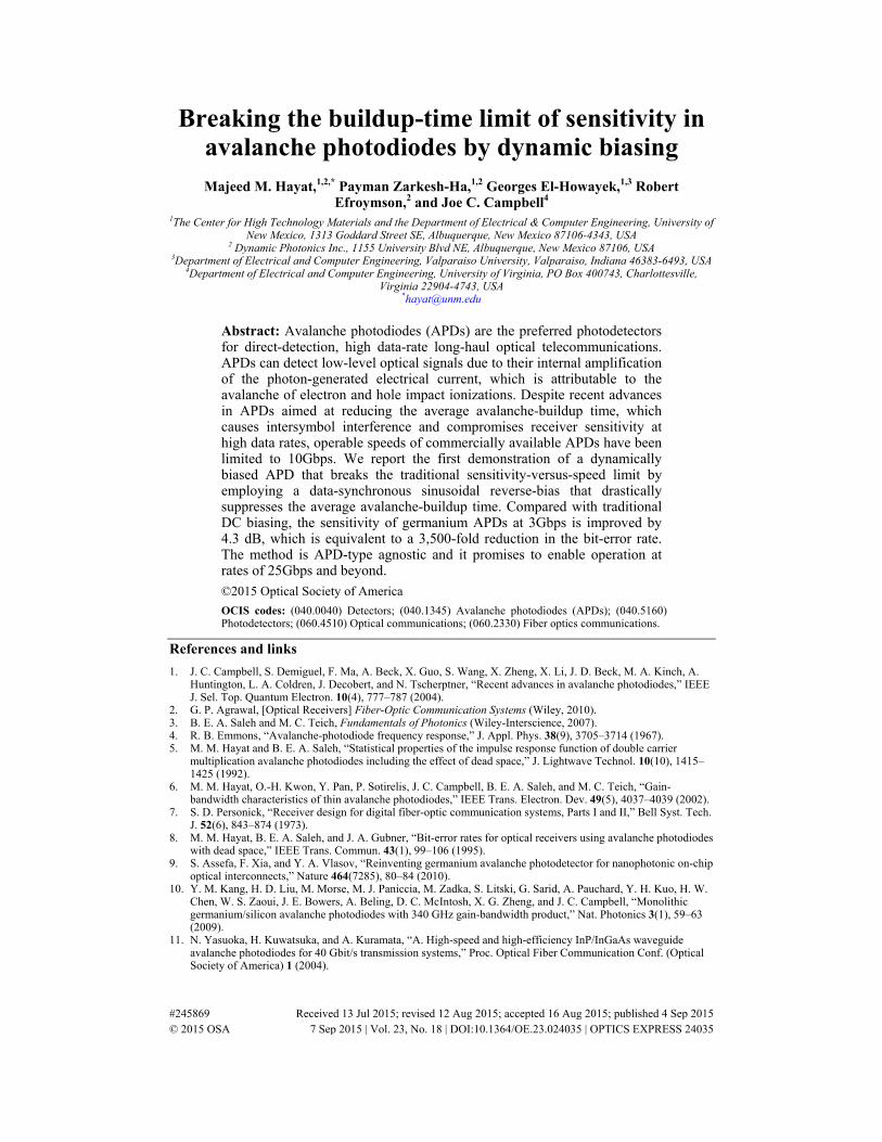
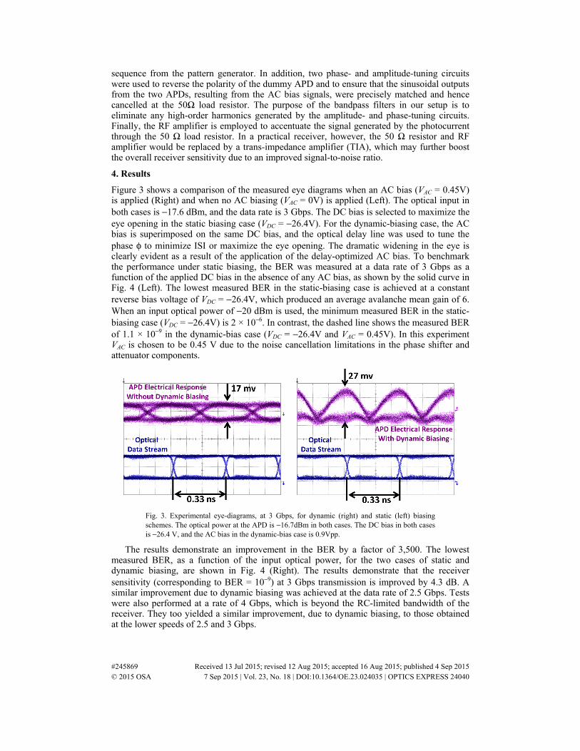
Figure 3 shows a comparison of the measured eye diagrams when an AC bias (VAC = 0.45V) is applied (Right) and when no AC biasing (VAC = 0V) is applied (Left). The optical input in both cases is −17.6 dBm, and the data rate is 3 Gbps. The DC bias is selected to maximize the eye opening in the static biasing case (VDC = −26.4V). For the dynamic-biasing case, the AC bias is superimposed on the same DC bias, and the optical delay line was used to tune the phase φ to minimize ISI or maximize the eye opening. The dramatic widening in the eye is clearly evident as a result of the application of the delay-optimized AC bias. To benchmark the performance under static biasing, the BER was measured at a data rate of 3 Gbps as a function of the applied DC bias in the absence of any AC bias, as shown by the solid curve in Fig. 4 (Left). The lowest measured BER in the static-biasing case is achieved at a constant reverse bias voltage of VDC = −26.4V, which produced an average avalanche mean gain of 6. When an input optical power of −20 dBm is used, the minimum measured BER in the static-biasing case (VDC = −26.4V) is 2 × 10⁻⁶. In contrast, the dashed line shows the measured BER of 1.1 × 10⁻⁹ in the dynamic-bias case (VDC = −26.4V and VAC = 0.45V). In this experiment VAC is chosen to be 0.45 V due to the noise cancellation limitations in the phase shifter and attenuator components.
Fig. 3. Experimental eye-diagrams, at 3 Gbps, for dynamic (right) and static (left) biasing schemes. The optical power at the APD is −16.7dBm in both cases. The DC bias in both cases is −26.4 V, and the AC bias in the dynamic-bias case is 0.9Vpp.
The results demonstrate an improvement in the BER by a factor of 3,500. The lowest measured BER, as a function of the input optical power, for the two cases of static and dynamic biasing, are shown in Fig. 4 (Right). The results demonstrate that the receiver sensitivity (corresponding to BER = 10−9) at 3 Gbps transmission is improved by 4.3 dB. A similar improvement due to dynamic biasing was achieved at the data rate of 2.5 Gbps. Tests were also performed at a rate of 4 Gbps, which is beyond the RC-limited bandwidth of the receiver. They too yielded a similar improvement, due to dynamic biasing, to those obtained at the lower speeds of 2.5 and 3 Gbps.
#245869 Received 13 Jul 2015; revised 12 Aug 2015; accepted 16 Aug 2015; published 4 Sep 2015 © 2015 OSA 7 Sep 2015 | Vol. 23, No. 18 | DOI:10.1364/OE.23.024035 | OPTICS EXPRESS 24040
Fig. 4. (Left) BER of the static-bias APD as a function of the reverse bias. Dashed line represents the BER corresponding to the dynamic bias. (Right) BER as a function of the optical power received by the APD for the dynamic-and static-bias cases.
To put the sensitivity improvement due to dynamic biasing in perspective, we use a known relationship between lowest receiver sensitivity (optimized over the reverse bias and avalanche-region width) and data rate for InP APD-based receivers (as extracted from Ong et al. [29]), to establish the correspondence between sensitivity improvement due to dynamic biasing and the expansion in operable data rate. More precisely, examination of Fig. 5 in [29] reveals that if an InP APD achieves the sensitivities S2 and S1 at the bit rates R1 and R2, respectively, then S2-S1 ≈11.3 × log10(R2/R1). This formula states that every 3.4 dB improvement in the sensitivity corresponds approximately to a two-fold increase in the operating bit rate. Equivalently, a 4.3dB improvement in the sensitivity due to dynamic biasing can be translated to an increase in the data rate by a factor of 2.4 compared to static biasing with the same sensitivity. Since Ge APDs are known to be slower and noisier than InP APDs [10] (k is closer to unity for Ge than that for InP [30, 31]), we can expect even higher sensitivity improvement in an InP APD than that demonstrated here for Ge APDs. In fact, a 4-5x improvement in the GBP was predicted theoretically for InP APDs [26], corresponding to a 10-15dB improvement in receiver sensitivity [32].
As we pointed out in the Introduction, the performance improvement is expected to be present in any APD operating in a regime where its performance is limited primarily by the buildup time (rather than being limited by RC effects or carrier transit time). Hence, the benefits of dynamic biasing are agnostic to the structure and material of APDs as long as the APDs are operated in the buildup-time limited regime.
5. Conclusions
In this paper, we have demonstrated, for the first time, that bit-synchronous dynamic biasing of an APD can significantly benefit the optical receiver speed and sensitivity in NRZ signaling by reducing the average avalanche buildup time and thus minimizing ISI. With proper packaging and design for high-speed operation, we anticipate that existing commercial 10 Gbps APDs may be operable at 25 Gbps bit rates or more, once optimized dynamic biasing is employed. The suppressing of the average buildup time can be additionally exploited to design APDs with wider multiplication regions than normally employed, without compromising their speed. This can serve to reduce the electric field in the multiplication layer, which would result in lower tunneling dark currents than those present in a fast APD that has a thin multiplication layer.
Acknowledgments
The authors thank Dr. Xiaoguang Zheng and Mr. Yaojia Chen for their assistance during the experiments at the University of Virginia. This work was supported in part by the National Science Foundation under the Smart Lighting ERC (Award EEC-0812056 / 1159201). Additional support was received from STC.UNM and Dynamic Photonic Inc.
#245869 Received 13 Jul 2015; revised 12 Aug 2015; accepted 16 Aug 2015; published 4 Sep 2015 © 2015 OSA 7 Sep 2015 | Vol. 23, No. 18 | DOI:10.1364/OE.23.024035 | OPTICS EXPRESS 24041