build digital tester - computer nerd kev's home on the web · 2016-12-20 · cover story/...
TRANSCRIPT

cover story/ cover story /cover story /cover story /cover story / covi
Here's that piece of dream
test equipment that can tell
you if a digital logic IC
is good or bad -section by section
Build R -E's Digital IC Tester HAVE YOU EVER WISHED YOU HAD A
fast, easy way to test the surplus digital IC's in your spare parts collection? Have you wanted to check an IC in -cir- cuit, under actual operating conditions? Wouldn't it be great to be able to moni- tor the logic states at several points on a digital circuit board ... even supply power to the board from an external source?
The DIGI -DYNA -CHECK is a truly dynamic digital integrated circuit checker that can be used to test digital IC's under actual operating conditions: it can be made to perform just as though it were functioning in an actual circuit. Tests can be performed both in- and out -of- circuit. A 5 -volt regulated supply, capable of delivering up to I
amp, is available within the DIGI- DYNA -CHECK to "fire up" fifteen or more IC's on a circuit board via an adapter cable with its miniature IC con-
necting clip. An internal "bounceless" pushbut-
ton, mounted on the front panel, can be used to advance counters, dividers, shift registers, etc., one step at a time. If de- sired, such IC's can be put through their paces automatically at a rate suitable for observing with an oscilloscope. This automatic mode of operation is avail- able via an internal 50-kHz conditioned clock with complementary outputs.
Connections to "the outside world ", ie., to equipment external to the DIGI -DYNA- CHECK, such as a scope, other voltage sources, oscillators, etc.. are easily made via eight 5 -way binding posts mounted on the front panel. Any internal or externally available function can be patched to any pin or com- bination of pins on the integrated cir- cuit under test by means of the matrix programmer in the DIGI -DYNA- CHECK."
by JACK CAZES
The heart of the checker is a 20-sli- der by 10- position matrix switch that is used to program the internal and /or ex- ternal functions and logic levels for the IC under test. Another article will de- scribe. in great detail, the programming and test procedures employed for a va- riety of digital integrated circuit types.
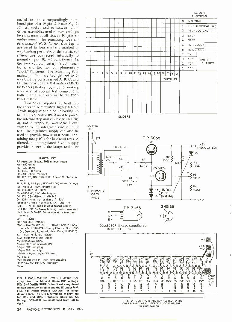
A schematic of the matrix switch used in the DIGI -DYNA -CHECK is in Fig. I. It shows the connections between the various functions and the pins of the IC being tested. Basically, it consists of twenty 10- position slide switches mounted together in a single frame, with corresponding positions on all switches wired together. Thus, when two or more sliders are in the same posi- tion, they are connected internally. Ad- ditionally, each slider has a "home" or neutral position (no connection to any other slider).
The first sixteen sliders are con-
MAY 1972 RADIO -ELECTRONICS 33
s
LM17
nected to the correspondingly num- bered pins of a 16 -pin DIP (see Fig. 2) IC test socket and to sixteen lamp - driver assemblies used to monitor logic levels present at all sixteen IC pins si- multaneously. The remaining four sli- ders, marked W, X, Y, and Z in Fig. 1,
are wired to four similarly marked S-
way binding posts. Six of the matrix po- sitions are connected internally to ground (logical 0), + 5 volts (logical 1), the two complementary "step" func- tions, and the two complementary "clock" functions. The remaining four matrix positions are brought out to S- way binding posts marked A, B, C, and D. This provides a 4 X 4 matrix (ABCD by WXYZ) that can be used for making a variety of special test connections, both internal and external to the DIGI- DYNA-CHECK.
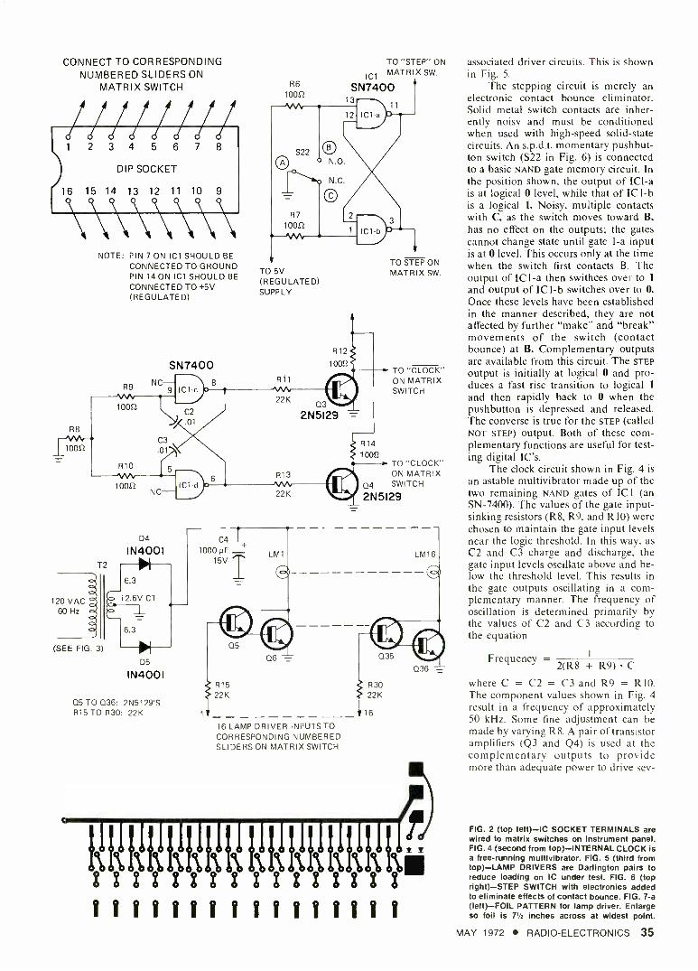
Two power supplies are built into the checker. A regulated, highly filtered 5 -volt supply capable of delivering up to 1 amp, continuously, is used to power the internal step and clock circuits (Fig. 4), and to supply V1.( and logic 1 level voltage to the integrated circuit under test. The regulated supply can also be used to provide power to a board con- taining many IC's for in- circuit tests. A filtered, but unregulated 5 -volt supply provides power to the lamps and their
PARTS LIST All resistors 1/2-watt 10% unless noted R1 -150 ohms R2 -220 ohms R3, R4 -100 ohms R5 -100 ohms, Trimpot R6, R7, R8, R9, R10, R12, R14 -100 ohms, Y.
watt R11, R13, R15 thru R30- 22,000 ohms, 1/. watt C1- 6000 µF, 15V, electrolytic C2, C3 -0.01 uF, 100V C4- 1000 1&F, 15V, electrolytic D1, D2, D3 -1N914 or 1N4148 D4, D5- 1N4001 or similar (OA, 50V) Rectifier Bridge -full wave, 1A, 100V PIV IC1 -SN -7400 (quad 2 -input NAND gates) BP1 thru BP16 -5 -way binding posts, insulated LM1 thru LM7 -4V, 50mA miniature lamp as-
sembly Q1-TIP-3055 Q2 thru Q36- 2N5129 Matrix Switch (S1 thru S20) -20 -pole 10 -posi-
tion (Part C10 -42A, Cherry Electric Co., 1650 Old Deerfield Road, Highland Park, III. 60035)
S21 -spst miniature toggle S22 -spdt miniature toggle Miscellaneous parts: 16 -pin DIP test sockets (2) 16-pin DIP test plug 16 -pin DIP test clip 16 -lead ribbon cable (21/2 feet) PC board Perf board with 0.1 -inch hole spacing Heat sink for TIP -3055 transistor Case
FIG. 1 (top)- MATRIX SWITCH layout. See cover photo for 14- and 16 -pin DIP settings. FIG. 3- POWER SUPPLY for 5 volts regulated to step and clock circuits and the IC under test. FIG. 7 -b (right) -PARTS LAYOUT for lamp - driver board. The C -B -E terminals at right are for Q35 and 036. Transistor pairs Q5 -06 through 033 -034 are positioned from left to right.
34 RADIO -ELECTRONICS MAY 1972
SLIDER POSITIONS
0. NEUTRAL
1. GND. (LOGICAL "0 ") 2. +5V (LOGICAL 1 ") 3. STEP
4. STEP
5. INT. CLOCK
6. INT. CLOCK
7. ,A INPUTS/
OUTPUTS
8. "B" g, C
10. "D" 1 2 3 4 5 6 7 8 9 10 1 1 1 2 13 14 1 5 16 W X Y Z
OUTPUTS
120 VAC 60 Hz
SLIDERS
RECT. BR.
ó
TO PRIMARY OF T2 (FIG. 5)
6.3V, 1
2A AC Ri
AC 15052
Cl +
6000 µ F
15V
TIP -3055 01
TIP -3055
COLLECTOR IS ALSO CONNECTED TO MOUNTING TAB
R2
2205
2N5129
Q2
D1 IN914 OR
D2 IN4148
T
411
2N5129 C
+ 5V (REGULATED)
D3
R3 1000
R5
10052
R4
1 oosz
o GND
6.3
CT & GND
0 6.3 C4
r r r r r r r r r r r r r r r r
- NJ (.4 A IX O) V OJ (O O N W A (I) O)
C B
E
C B
R15 R16 R17 R18 R19 R20 R21 R22 R23 R24 R25 R26 R27 R28 R29 R30
1 2 3 4 5 6 7 8 9 10 11 12 13 14 15 16
LAMP COM & C4
THESE DRIVER INPUTS ARE CONNECTED TO THE CORRESPONDING NUMBERED SLIDERS ON THE
MATRIX SWITCH.
CONNECT TO CORRESPONDING NUMBERED SLIDERS ON
MATRIX SWITCH
NOTE: PIN 7 ON IC1 SHOULD BE
CONNECTED TO GROUND PIN 14 ON IC1 SHOULD BE CONNECTED TO +5V (REGULATED)
R9
SN7400
TO "STEP" ON
ICI MATRIX SW.
R6 SN7400 13
10052
TO 5V (REGULATED) SUPPLY
120 VAC 60 Hz
(SEE FIG. 3)
D4
1N4001 C4
1000 µ F
15V LM1
12.6V CT
Q5
D5
1N4001
Q5 TO Q36: 2N5129'S R15 TO R30: 22K
R15 22K
Q6 -
16 LAMP DRIVER INPUTS TO
CORRESPONDING NUMBERED SLIDERS ON MATRIX SWITCH
TO STEP ON MATRIX SW.
TO "CLOCK" ON MATRIX SWITCH
TO "CLOCK" ON MATRIX SWITCH
' 11d1t ididll ti tiI1 iid111d 8888888888888888 rrrrtrttrtrrrtrt
associated driver circuits. This is shown in Fig. 5.
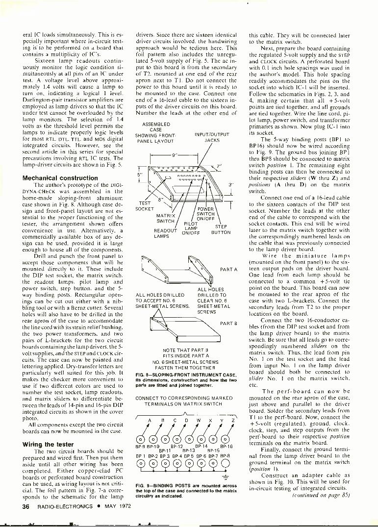
The stepping circuit is merely an electronic contact bounce eliminator. Solid metal switch contacts are inher- ently noisy and must be conditioned when used with high -speed solid -state circuits. An s.p.d.t. momentary pushbut- ton switch (S22 in Fig. 6) is connected to a basic NAND gate memory circuit. In the position shown, the output of ICl -a is at logical 0 level, while that of IC 1 -b is a logical 1. Noisy, multiple contacts with C, as the switch moves toward B, has no effect on the outputs; the gates cannot change state until gate 1 -a input is at O level. This occurs only at the time when the switch first contacts B. The output of IC 1 -a then swithces over to 1
and output of ICI -b switches over to O.
Once these levels have been established in the manner described, they are not affected by further "make" and "break" movements of the switch (contact bounce) at B. Complementary outputs are available from this circuit. The STEP
output is initially at logical 0 and pro- duces a fast rise transition to logical 1
and then rapidly back to 0 when the pushbutton is depressed and released. The converse is true for the STEP (called NOT STEP) output. Both of these com- plementary functions are useful for test- ing digital IC's.
The clock circuit shown in Fig. 4 is an astable multivibrator made up of the two remaining NAND gates of IC 1 (an SN- 7400). The values of the gate input - sinking resistors (R8, R9, and RIO) were chosen to maintain the gate input levels near the logic threshold. In this way, as C2 and C3 charge and discharge, the gate input levels oscillate above and be- low the threshold level. This results in the gate outputs oscillating in a corn- plementary manner. The frequency of oscillation is determined primarily by the values of C2 and C3 according to the equation
Frequency = 2(R8 + R9) C
where C = C2 = C3 and R9 = R 10.
The component values shown in Fig. 4 result in a frequency of approximately 50 kHz. Some fine adjustment can be made by varying R8. A pair of transistor amplifiers (Q3 and Q4) is used at the complementary outputs to provide more than adequate power to drive sev-
1
FIG. 2 (top left) -IC SOCKET TERMINALS are wired to matrix switches on Instrument panel. FIG. 4 (second from top) -INTERNAL CLOCK is a free -running multivibrator. FIG. 5 (third from top) -LAMP DRIVERS are Darlington pairs to reduce loading on IC under test. FIG. 6 (top right) -STEP SWITCH with electronics added to eliminate effects of contact bounce. FIG. 7 -a (left) -FOIL PATTERN for lamp driver. Enlarge so foil is 7'/2 inches across at widest point.
MAY 1972 RADIO -ELECTRONICS 35
eral IC loads simultaneously. This is es- pecially important where in- circuit test- ing is to be performed on a board that contains a multiplicity of IC's.
Sixteen lamp readouts contin- uously monitor the logic condition si- multaneously at all pins of an IC under test. A voltage level above approxi- mately 1.4 volts will cause a lamp to turn on, indicating a logical 1 level. Darlington -pair transistor amplifiers are employed as lamp drivers so that the IC under test cannot be overloaded by the lamp monitors. The selection of 1.4 volts as the threshold level permits the lamps to indicate properly logic levels for most RTL. DTL. TTL, and MOS digital integrated circuits. However, see the second article in this series for special precautions involving RTL IC tests. The lamp- driver circuits are shown in Fig. 5.
Mechanical construction The author's prototype of the DIGI-
DYNA -CHECK was assembled in the home -made sloping -front aluminum case shown in Fig. 8. Although case de- sign and front -panel layout are not es- sential to the proper functioning of the tester, the arrangement shown offers convenience in use. Alternatively, a commercially available box of any de- sign can be used, provided it is large enough to house all of the components.
Drill and punch the front panel to accept those components that will be mounted directly to it. These include the DIP test socket, the matrix switch, the readout lamps, pilot lamp and power switch, step button, and the S-
way binding posts. Rectangular open- ings can be cut out either with a nib- bling tool or with a Bernz cutter. Several holes will also have to be drilled in the rear apron of the case to accommodate the line cord with its strain relief bushing, the two power transformers, and two pairs of L- brackets for the two circuit boards containing the lamp drivers, the 5-
volt supplies, and the STEP and CLOCK cir- cuits. The case can now be painted and lettering applied. Dry- transfer letters are particularly well suited for this job. It makes the checker more convenient to use if two different colors are used to number the test socket, lamp readouts, and matrix sliders to differentiate be- tween the leads of 14-pin and 16 -pin DIP integrated circuits as shown in the cover photo.
All components except the two circuit boards can now be mounted in the case.
Wiring the tester The two circuit boards should be
prepared and wired first. Then put them aside until all other wiring has been completed. Either copper -clad PC boards or perforated board construction can be used, as wiring layout is not criti- cial. The foil pattern in Fig. 7 -a corre- sponds to the schematic for the lamp
36 RADIO -ELECTRONICS MAY 1972
drivers. Since there are sixteen identical driver circuits involved, the handwiring approach would be tedious here. This foil pattern also includes the unregu- lated 5 -volt supply of Fig. 5. The ac in- put to this board is from the secondary of T2, mounted at one end of the rear apron next to T1. Do not connect the power to this board until it is ready to be mounted to the case. Connect one end of a 16 -lead cable to the sixteen in- puts of the driver circuits on this board. Number the leads at the other end of
ASSEMBLED CASE
SHOWING FRONT - PANEL LAYOUT
9.,
INPUT /OUTPUT JACKS
TEST 8
SOCKET
MATRIX SWITCH
READOUT LAMPS
POWER SWITCH ON /OFF
PILOT STEP TEP
ON /OFF BUTTON
3"
ALL HOLES DRILLED TO ACCEPT NO. 6 SHEET -METAL SCREWS.
PART A
ALL HOLES DRILLED TO CLEAR NO. 6
SHEET -METAL SCREWS
NOTE THAT PART B
FITS INSIDE PART A
NO. 6 SHEET -METAL SCREWS FASTEN THEM TOGETHER
FIG. 8- SLOPING -FRONT INSTRUMENT CASE. its dimensions. construction and how the two parts are fitted and joined together.
CONNECT TO CORRESPONDING MARKED TERMINALS ON MATRIX SWITCH
A B C D W X Y Z ad'a BP-9 BP-10 BP-12 BP-14 BP-16
BP-11 BP-13 BP-15 BP-1 BP-2 BP-3 BP-4 BP-5 BP-6 BP-7 BP-8
FIG. 9- BINDING POSTS are mounted across the top of the case and connected to the matrix circuitry as indicated.
this cable. They will be connected later to the matrix switch.
Next, prepare the board containing the regulated 5 -volt supply and the STEP
and CLOCK circuits. A perforated board with 0.1 inch hole spacings was used in the author's model. This hole spacing readily accommodates the pins on the socket into which IC -1 will be inserted. Follow the schematics in Figs. 2, 3, and 4, making certain that all + 5-volt points are tied together, and all grounds are tied together. Wire the line cord, pi- lot lamp, power switch, and transformer primaries as shown. Now plug IC -1 into its socket.
The 5 -way binding posts (BP1 to BP 16) should now be wired according to Fig. 9. The ground bus joining BP 1
thru BP8 should be connected to matrix switch position 1. The remaining eight binding posts can then be connected to their respective sliders (W thru Z) and positions (A thru D) on the matrix switch.
Connect one end of a 16 -lead cable to the sixteen contacts of the DIP test socket. Number the leads at the other end of the cable to correspond with the socket contacts. This end will be wired later to the matrix switch together with the correspondingly numbered leads on the cable that was previously connected to the lamp driver board.
Wire the miniature lamps (mounted on the front panel) to the six- teen output pads on the driver board. One lead from each lamp should be connected to a common +5 -volt tie point on the board. This board can now be mounted to the rear apron of the case with two L- brackets. Connect the secondary leads from T2 to the proper locations on the board.
Connect the two 16- conductor ca- bles (from the DIP test socket and from the lamp driver board) to the matrix switch. Be sure that all leads go to corre- spondingly numbered sliders on the matrix switch. Thus, the lead from pin No. 1 on the test socket and the lead from input No. 1 on the lamp driver board should both be connected to slider No. 1 on the matrix switch, etc.
The perf -board can now be mounted on the rear apron of the case, just above and parallel to the driver board. Solder the secondary leads from T1 to the perf -board. Now, connect the +5 -volt (regulated), ground, clock, clock, step, and step outputs from the perf -board to their respective position terminals on the matrix board.
Finally, connect the ground termi- nal from the lamp driver board to the ground terminal on the matrix switch (position 1).
Construct an adapter cable as shown in Fig. 10. This will be used for in- circuit testing of integrated circuits.
(continued on page 85)

IC TESTER
(continued from page 36)
Testing Plug the Digi -Dyna -Check into a
120 -volt, 60-Hz supply and turn on the power switch. Adjust R5 on the perfboard to obtain exactly 5 volts at
the output of the regulated power sup- ply. This should be measured with a
16-CONDUCTOR CABLE
DIP PLUG
CLIP 1
LEAD NO. 1
FIG. 10- ADAPTER CABLE consists of 16 -pin plug and clamp and is used for in- circuit testing of DIP -type integrated circuits.
VTVM, an FET input voltmeter, or other similar high input- impedance de- vice. With all matrix sliders in the neu- tral position, only the pilot lamp should be on. Move sliders 1 thru 20 to position
1 (ground). None of the lamps should light. All IC test socket pins and binding posts W thru Z should be shorted together and at ground level. (Check with an ohmmeter). Move all sliders to position 2 ( + 5V). All sixteen readouts should be on. All DIP test socket pins and binding posts W thru Z should be at +5- volts. Move all sliders to position 3 (Step). All socket pins should be at logical 0 to- gether with binding posts W thru Z. De- pressing the STEP button should cause all lamps to turn on and bring all socket pins and binding posts W thru Z to logi- cal 1. Releasing the STEP button should return everything to their initial states. Move all sliders to position 4 (Step). Ev- erything should behave as the inverse of that described for position 3. Move all sliders to position 5 (Clock). All lamps should glow at half brilliance due to the 50% duty cycle of the square wave clock output. A 50 kHz square wave should be present at all DIP test socket pins and at binding posts W thru Z. With all sliders at position 6 (Clock) you should see the inverse of that observed for po- sition 5. Wave forms in positions 5 and 6 can be observed with a scope at bind- ing posts W thru Z. Moving any of the
sliders to any of the four positions 7 thru 10 should connect their corresponding circuits to binding posts A thru D, re- spectively.
If everything described here checks out A -OK, you're ready to use your Digi -Dyna -Check to check IC's. R -E
BUILD A SOLID -STATE LASER Our June cover feature presents complete construction details of a solid -state laser. It's both easy and inexpensive to build. If you've been waiting for a low -cost low -power "safe" laser to experiment with you won't want to miss the June issue of Radio -Electronics.
People In Trouble Need Your
UNITED GIFT
If you don't do it, It won't get done
TV TUNER SERSIICE VHF, UHF, FM or IF-Subchassis...
... All Makes
g(if1rf... b
Tast 8hr. Service!
You owe it to yourself to try P.T.S. We are the fastest growing, oldest and now the largest tuner service company in the world. Here is what you get.
1. Fastest Service -8 hr. -in and out the same day. Overnight transit to one of our six plants, for parts, tuners or IF- modules.
2. All tuners cleaned inside and out, repaired, realigned and air tested.
3. On IFmodules all stages checked, all traps set with high calibre test equipment.
4. Fine Quality! Your customers are satisfied and you are not bothered with returning your units for rework!
5. Lower Cost! Up to $5.50 less than other tuner companies!
6. Friendly, helpful personalized service!
1 YEAR GUARANTEE
LIKE TO DO IT
PTS makes all tuner parts available to you.
Send one dollar (redeemable) for our TUNER RE- PLACEMENT GUIDE AND PARTS CATALOG
FIRST TO OFFER 365 -DAY GUARANTEE! COLOR -BLACK & WHITE -- TRANSISTOR TUNERS -
ALL MAKES GUARANTEED COLOR ALIGNMENT -
NO ADDITIONAL CHARGE
YOURSELF?
60 pages of top information Blow -up of all tuners Largest exact tuner replacement guide
Antenna Coil Replacement Guide Multi -fit Replacement Tuner Shaft Guide
We offer you finer, faster...
For fastest sere¢e, send faulty unit with tubes. shields and all broken paris to
PTS ELECTRONICS, INC.
HOME OFFICE- SOUTHEAST- WEST COAST- EAST- SOUTHWEST- MOUNTAIN-
VHF UHF-FM
OAST- EAST- SOUTHWEST- MOUNTAIN-
VHF -UHF -FM $ 9.95 UV -COMBO $16.95 IF- MODULE $12.50
Major Parts charged at Net Price
CUSTOMIZED REPLACEMENTS AVAILABLE FOR $12 95 UP (NEW OR REBUILT)
P.O. Box 272 -Bloomington, Ind. 47401 P.O. Box 6771 -Jacksonville, Fla. 32205 P.O. Box 41354- Sacramento, Calif. 95841 P.O. Box 3189 -Springfield, Mass. 01103 P.O. Box 7332 -Longview, Tex. 75601 P.O. Box 4145- Denver, Colo. 80204
Circle 67 on reader service card MAY 1972 RADIO- ELECTRONICS 85
Tel. 812/824-9331 Tel. 904/389-9952 Tel. 916/482.6220 Tel. 413/734 -2737 Tel. 214/753 -4334 Tel. 303/244 -2818
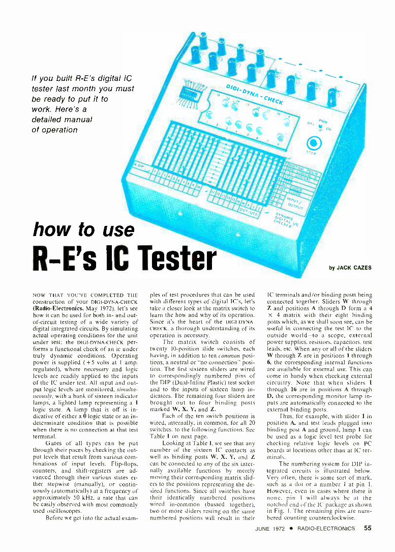
If you built R -E's digital IC tester last month you must be ready to put it to work. Here's a
detailed manual of operation
----_
how to use
R -E's IC Testir NOW THAT YOU'VE COMPLETED THE construction of your DIGI -DYNA -CHECK (Radio -Electronics, May 1972), let's see how it can be used for both in- and out - of- circuit testing of a wide variety of digital integrated circuits. By simulating actual operating conditions for the unit under test; the DIGI -DYNA -CHECK per- forms a functional check of an is under truly dynamic conditions. Operating power is supplied ( +5 volts at 1 amp, regulated), where necessary and logic levels are readily applied to the inputs of the IC under test. All input and out- put logic levels are monitored, simulta- neously, with a bank of sixteen indicator lamps, a lighted lamp representing a 1
logic state. A lamp that is off is in- dicative of either a O logic state or an in- determinate condition that is possible when there is no connection at that test terminal.
Gates of all types can be put through their paces by checking the out- put levels that result from various com- binations of input levels. Flip -flops, counters, and shift -registers are ad- vanced through their various states ei- ther stepwise (manually), or contin- uously (automatically) at a frequency of approximately 50 kHz, a rate that can be easily observed with most commonly used oscilloscopes.
Before we get into the actual exam-
pies of test procedures that can be used with different types of digital IC's, let's take a closer look at the matrix switch to learn the how and why of its operation. Since it's the heart of the DIGI -DYNA- CHECK, a thorough understanding of its operation is necessary.
The matrix switch consists of twenty 10- position slide switches, each having, in addition to ten common posi- tions, a neutral or "no connection" posi- tion. The first sixteen sliders are wired to correspondingly numbered pins of the DIP (Dual -Inline Plastic) test socket and to the inputs of sixteen lamp in- dicators. The remaining four sliders are brought out to four binding posts marked W, X, Y, and Z.
Each of the ten switch positions is wired, internally, in common, for all 20 switches, to the following functions. See Table I on next page.
Looking at Table I, we see that any number of the sixteen IC contacts as well as binding posts W, X, Y, and Z can be connected to any of the six inter- nally available functions by merely moving their corresponding matrix slid- ers to the positions representing the de- sired functions. Since all switches have their identically numbered positions wired in- common (bussed together), two or more sliders resting on the same numbered positions will result in their
by JACK CAZES
IC terminals and /or binding posts being connected together. Sliders W through Z and positions A through D form a 4 x 4 matrix with their eight binding posts which, as we shall soon see, can be useful in connecting the test IC to the outside world -to a scope, external power supplies, resistors, capacitors, test leads, etc. When any or all of the sliders W through Z are in positions 1 through 6, the corresponding internal functions are available for external use. This can come in handy when checking external circuitry. Note that when sliders 1
through 16 are in positions A through D, the corresponding monitor lamp in- puts are automatically connected to the external binding posts.
Thus, for example, with slider 1 in position A, and test leads plugged into binding post A and ground, lamp 1 can be used as a logic level test probe for checking relative logic levels on PC boards at locations other than at IC ter- minals.
The numbering system for DIP in- tegrated circuits is illustrated below. Very often, there is some sort of mark, such as a dot or a number 1 at pin 1.
However, even in cases where there is none. pin I will always be at the notched end of the IC package as shown in Fig. 1. The remaining pins are num- bered counting counterclockwise.
JUNE 1972 RADIO -ELECTRONICS 55
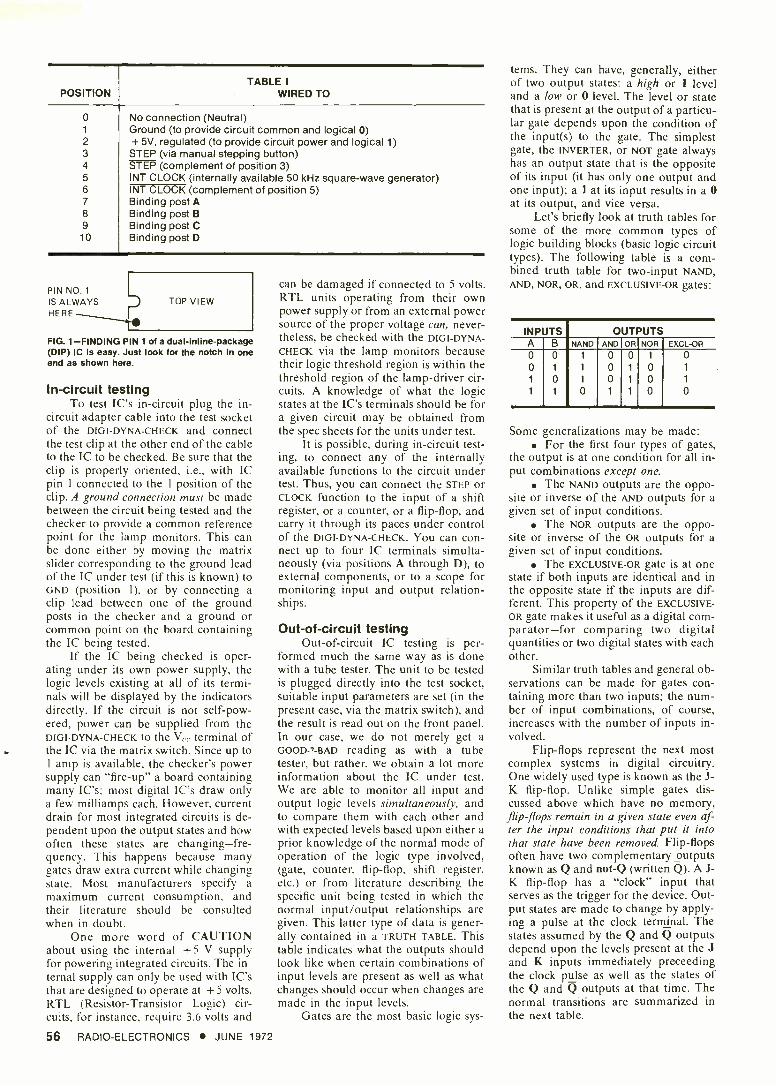
POSITION TABLE I
WIRED TO
0 No connection (Neutral) 1 Ground (to provide circuit common and logical 0) 2 + 5V, regulated (to provide circuit power and logical 1) 3 STEP (via manual stepping button) 4 STEP (complement of position 3) 5 INT CLOCK (internally available 50 kHz square -wave generator) 6 INT CLOCK (complement of position 5) 7 Binding post A 8 Binding post B 9 Binding post C
10 Binding post D
PIN NO. 1
IS ALWAYS TOP VI FAN
FIG. 1- FINDING PIN 1 of a dual -inline- package (DIP) IC is easy. Just look for the notch in one end as shown here.
In- circuit testing To test IC's in- circuit plug the in-
circuit adapter cable into the test socket of the DIGI -DYNA -CHECK and connect the test clip at the other end of the cable to the IC to be checked. Be sure that the clip is properly oriented, i.e., with IC pin I connected to the 1 position of the clip. A ground connection must be made between the circuit being tested and the checker to provide a common reference point for the lamp monitors. This can be done either by moving the matrix slider corresponding to the ground lead of the IC under test (if this is known) to GND (position 1), or by connecting a clip lead between one of the ground posts in the checker and a ground or common point on the board containing the IC being tested.
If the IC being checked is oper- ating under its own power supply, the logic levels existing at all of its termi- nals will be displayed by the indicators directly. If the circuit is not self -pow- ered, power can be supplied from the DIGI -DYNA -CHECK to the Ve,. terminal of the IC via the matrix switch. Since up to 1 amp is available, the checker's power supply can "fire -up" a board containing many IC's; most digital IC's draw only a few milliamps each. However, current drain for most integrated circuits is de- pendent upon the output states and how often these states are changing -fre- quency. This happens because many gates draw extra current while changing state. Most manufacturers specify a maximum current consumption, and their literature should be consulted when in doubt.
One more word of CAUTION about using the internal +5 V supply for powering integrated circuits. The in- ternal supply can only be used with IC's that are designed to operate at +5 volts. RTL (Resistor- Transistor Logic) cir- cuits, for instance, require 3.6 volts and
56 RADIO -ELECTRONICS JUNE 1972
can be damaged if connected to 5 volts. RTL units operating from their own power supply or from an external power source of the proper voltage can, never- theless, be checked with the DIGI -DYNA- CHECK via the lamp monitors because their logic threshold region is within the threshold region of the lamp -driver cir- cuits. A knowledge of what the logic states at the IC's terminals should be for a given circuit may be obtained from the spec sheets for the units under test.
It is possible, during in- circuit test- ing, to connect any of the internally available functions to the circuit under test. Thus, you can connect the STEP or CLOCK function to the input of a shift register, or a counter, or a flip -flop, and carry it through its paces under control of the DIGI -DYNA- CHECK. You can con- nect up to four IC terminals simulta- neously (via positions A through D), to external components, or to a scope for monitoring input and output relation- ships.
Out -of- circuit testing Out -of- circuit IC testing is per-
formed much the same way as is done with a tube tester. The unit to be tested is plugged directly into the test socket, suitable input parameters are set (in the present case, via the matrix switch), and the result is read out on the front panel. In our case, we do not merely get a GOOD -? -BAD reading as with a tube tester, but rather, we obtain a lot more information about the IC under test. We are able to monitor all input and output logic levels simultaneously, and to compare them with each other and with expected levels based upon either a prior knowledge of the normal mode of operation of the logic type involved, (gate, counter, flip -flop, shift register, etc.) or from literature describing the specific unit being tested in which the normal input /output relationships are given. This latter type of data is gener- ally contained in a TRUTH TABLE. This table indicates what the outputs should look like when certain combinations of input levels are present as well as what changes should occur when changes are made in the input levels.
Gates are the most basic logic sys-
tems. They can have, generally, either of two output states: a high or 1 level and a low or 0 level. The level or state that is present at the output of a particu- lar gate depends upon the condition of the input(s) to the gate. The simplest gate, the INVERTER, or NOT gate always has an output state that is the opposite of its input (it has only one output and one input); a 1 at its input results in a 0 at its output, and vice versa.
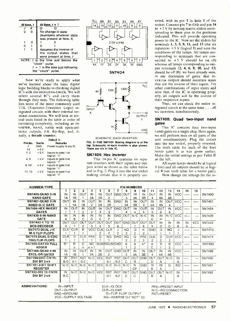
Let's briefly look at truth tables for some of the more common types of logic building blocks (basic logic circuit types). The following table is a corn- bined truth table for two -input NAND, AND, NOR, OR, and EXCLUSIVE -OR gates:
INPUTS OUTPUTS A B NAND AND OR NOR EXCL -OP
0 0 1 0 0 1 0
0 1 1 0 1 0 1
1 0 1 0 1 0 1
1 1 0 1 1 o o
Some generalizations may be made: For the first four types of gates,
the output is at one condition for all in- put combinations except one.
The NAND outputs are the oppo- site or inverse of the AND outputs for a given set of input conditions.
The NOR outputs are the oppo- site or inverse of the OR outputs for a given set of input conditions.
The EXCLUSIVE -OR gate is at one state if both inputs are identical and in the opposite state if the inputs are dif- ferent. This property of the EXCLUSIVE - OR gate makes it useful as a digital com- parator -for comparing two digital quantities or two digital states with each other.
Similar truth tables and general ob- servations can be made for gates con- taining more than two inputs; the num- ber of input combinations, of course, increases with the number of inputs in- volved.
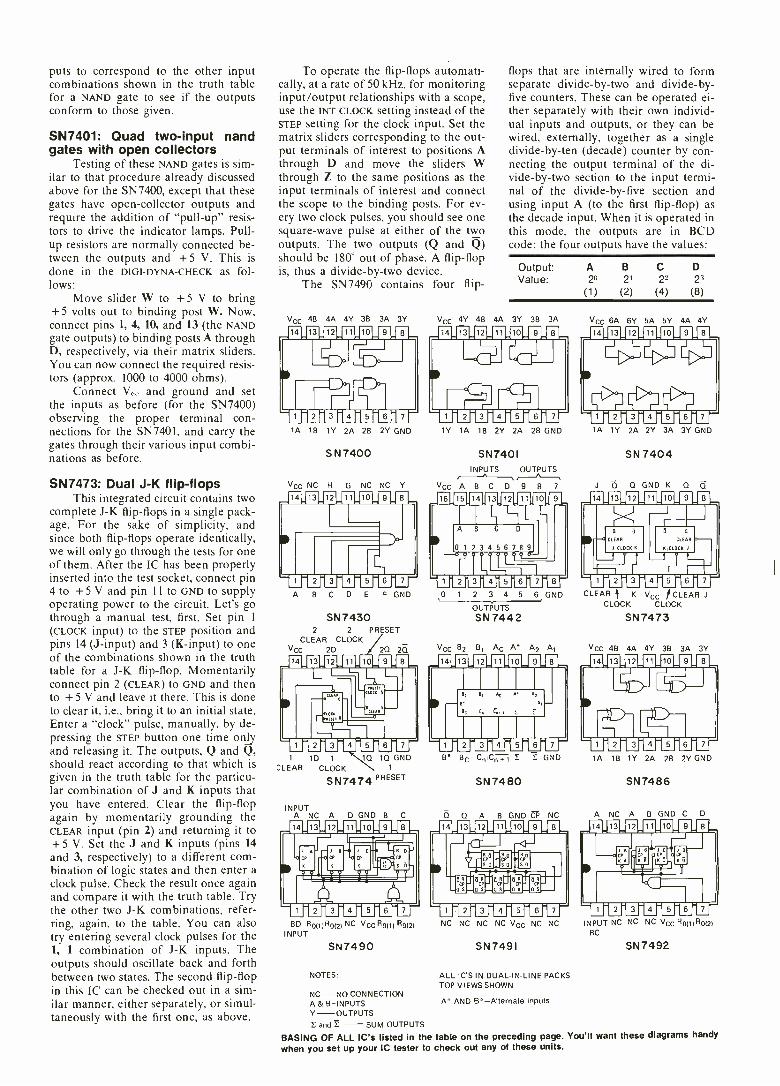
Flip -flops represent the next most complex systems in digital circuitry. One widely used type is known as the J- K flip -flop. Unlike simple gates dis- cussed above which have no memory, flip -flops remain in a given state even af- ter the input conditions that put it into that state have been removed. Flip -flops often have two complementary outputs known as Q and not -Q (written Q). A J- K flip -flop has a "clock" input that serves as the trigger for the device. Out- put states are made to change by apply- ing a pulse at the clock terminal. The states assumed by the Q and Q outputs depend upon the levels present at the J and K inputs immediately preceeding the clock pulse as well as the states of the Q and Q outputs at that time. The normal transitions are summarized in the next table.
At time, t At time, f + 1
J K Q Q No change in state (maintains whatever state was present at time, t) 1 0 0 1
Assumes the inverse of the output states that were present at time, t
NOTE: t is the time just before the "clock" pulse. t + 1 is the time just following the "clock" pulse.
0 0
1 0
0 1
1 1
Now we're ready to apply what we've learned about the basic digital logic building blocks to checking digital IC's with the DIGI- DYNA -CHECK. We will select several IC's and carry them through their tests. The following table lists some of the more commonly used TTL (Transistor- Transistor Logic) in- tegrated circuits with their internal ter- minal connections. We will look at sev- eral units listed in the table in order of increasing complexity, including an IN-
VERTER, NAND, NAND with open -col- lector outputs, J -K flip -flop, and, fi-
nally, a decade counter. TABLE II
Pin No. Set to Remarks 7 GND Power supply to the IC 14 +5V 1,2 +5V
4,5 +5V
9, 10 +5v
12,13 +5V
Inputs to gate 1 at logical "1" Inputs to gate 2 at logical "1" Inputs to gate 3 at logical "1" Inputs to gate 4 at logical "1"
Vcc 6A 6Y 5A 5Y 4A 4Y
1A 1Y 2A 2Y 3A
SN7404
3Y GND
SCHEMATIC (EACH INVERTER)
FIG. 2 -THE SN7404. Basing diagram is at the top. Schematic of each inverter is also shown. There are six in this IC.
SN7404: Hex inverter This 14 -pin IC contains six sepa-
rate inverters with their inputs and out- puts wired as shown in the table below and in Fig. 2. Plug it into the test socket making certain that it is properly ori-
ented, with its pin 1 in hole 1 of the socket. Connect pin 7 to GND and pin 14
to +5 V by moving matrix sliders corre- sponding to these pins to the positions indicated. This will provide operating power to the IC. Now set the sliders for terminals 1, 3, 5, 9, 11, and 13 (the six inputs) to +5 V (logical 1) and note the conditions of the lamps. All lamps cor- responding to terminals that are con- nected to +5 V should be on (1) whereas all lamps corresponding to out- put terminals (2, 4, 6, 8, 10, and 12) should be off (0): we have already seen, in our discussion of gates. that IN-
VERTER outputs should maintain states that are the inverse of their inputs. Try other combinations of input states and note that, if the IC is operating prop- erly, all outputs will be the inverse of their respective inputs.
Thus, we can check the entire in- tegrated circuit at the same time . . . all six inverters, simultaneously.
SN7400: Quad two -input nand gates
This IC contains four two -input NAND gates on a single chip. Here again, we will perform tests on all parts of the unit simultaneously. Plug the circuit into the test socket, properly oriented. The truth table for each of the four NAND gates is as was given earlier. Make the initial settings as per Table II at the left.
All input lamps should be at logical 1 (on) and all outputs should be at logi- cal 0 (see truth table for a NAND gate).
Now change the settings for the in-
NUMBER /TYPE PIN NUMBERS
SN7400 -QUAD 2 -IN NAND GATE
1
IN 1A
2 IN
1B
3 OUT
1
4 IN 2A
5
IN
2B
6
OUT 2
7
GND 8
OUT 3
9 IN
3A
10 IN 3B
11
OUT 4
12 IN
4A
13 IN 4B
14 VCC
15 -- 16 -- SN7400
SN7401 -QUAD 2 -IN NAND -O /C GATE
OUT 1
IN
1A IN 1B
OUT 2
IN
2A IN 2B
GND IN 3A
IN 3B
OUT 3
IN 4A
IN
4B OUT
4
VCC -- -- SN7401
SN7404 -HEX INVERT GATES
IN 1
OUT 1
IN 2
OUT 2
IN
3 OUT
3 GND OUT
4 IN
4 OUT
5 IN 5
OUT 6
IN
6 VCC -- -- SN7404
SN7430 -8 -IN NAND GATE
IN A
IN B
IN
C IN D
IN E
IN F
GND OUT N/C N/C IN
G
IN
H
N/C VCC -- -- SN7430
SN7442 -4 TO 10 BCD DECODER
OUT 0
OUT 1
OUT 2
OUT 3
OUT 4
OUT 5
OUT 6
GND OUT 7
OUT 8
OUT 9
IN
D
IN
C IN B
IN A
VCC SN7442
SN7473 DUAL J -K M -S FLIP -FLOPS
CLK 1
CLR 1
K 1
VCC CLK 2
CLR 2
J
2
NO 2
Q 2
K
2 GND Q
1
NQ 1
J
1
-- -- SN7473
SN7474 -DUAL D -EDG TRIG FLIP -FLOPS
CLR 1
D
1
CLK 1
PRE 1
Q 1
NQ 1
GND NQ 2
Q 2
PRE 2
CLK 2
D
2
CLR 2
VCC -- -- SN7474
SN7480 -GATED FULL ADDER
Ba B
c C n
NC n+ 1
SUM NSUM GND A 1
A 2
A* A C
B
1
B
2
VCC -- -- SN7480
SN7486 -QUAD 2 -IN EXCL -OR GATES
IN 1A
IN 1B
OUT 1
IN 2A
IN
2B OUT
2
GND OUT 3
IN 3A
IN
3B OUT
4
IN 4A
IN
4B VCC -- -- SN7486
SN7490 -DEC CNTR- DIV BY 2 +5
IN B -D
RST 0 -1
RST 0 -2
N /C VCC RST 9 -1
RST 9 -2
OUT C
OUT B
GND OUT D
OUT A
N /C IN
A -- -- SN7490
SN7491 -8 BIT SHIFT REGISTER
N/C N/C N/C N/C VCC N/C N/C N/C N
CP GND IN
B
IN A
Q NQ -- -- SN7491
SN7492 -DIV 12 -CNTR DIV BY 2+6
IN B -C
N/C N/C N/C VCC RST 0 -1
RST 0 -2
OUT D
OUT C
GND OUT B
OUT A
N/C IN A
-- -- SN7492
ABBREVIATIONS: IN -INPUT OUT -OUTPUT GND- GROUND VCC- SUPPLY VOLTAGE
CLK -CLOCK CUR-CLEAR
Q -FLIP FLOP OUTPUT NO- INVERSE Q ( "NOT" Q)
PRE -PRESET INPUT N /C -NO CONNECTION RST -RESET
JUNE 1972 RADIO -ELECTRONICS 57
puts to correspond to the other input combinations shown in the truth table for a NAND gate to see if the outputs conform to those given.
SN7401: Quad two -input nand gates with open collectors
Testing of these NAND gates is sim- ilar to that procedure already discussed above for the SN7400, except that these gates have open -collector outputs and require the addition of "pull -up" resis- tors to drive the indicator lamps. Pull - up resistors are normally connected be- tween the outputs and +5 V. This is done in the DIGI -DYNA -CHECK as fol- lows:
Move slider W to +5 V to bring +5 volts out to binding post W. Now, connect pins 1, 4, 10, and 13 (the NAND gate outputs) to binding posts A through D, respectively, via their matrix sliders. You can now connect the required resis- tors (approx. 1000 to 4000 ohms).
Connect V, and ground and set the inputs as before (for the SN7400) observing the proper terminal con- nections for the SN7401, and carry the gates through their various input combi- nations as before.
SN7473: Dual J -K flip -flops This integrated circuit contains two
complete J -K flip -flops in a single pack- age. For the sake of simplicity, and since both flip -flops operate identically, we will only go through the tests for one of them. After the IC has been properly inserted into the test socket, connect pin 4 to +5 V and pin 11 to GND to supply operating power to the circuit. Let's go through a manual test, first. Set pin 1
(CLOCK input) to the STEP position and pins 14 (J- input) and 3 (K- input) to one of the combinations shown in the truth table for a J -K flip -flop. Momentarily connect pin 2 (CLEAR) to GND and then to +5 V and leave it there. This is done to clear it, i.e., bring it to an initial state. Enter a "clock" pulse, manually, by de- pressing the STEP button one time only and releasing it. The outputs, Q and Q, should react according to that which is given in the truth table for the particu- lar combination of J and K inputs that you have entered. Clear the flip -flop again by momentarily grounding the CLEAR input (pin 2) and returning it to +5 V. Set the J and K inputs (pins 14
and 3, respectively) to a different com- bination of logic states and then enter a clock pulse. Check the result once again and compare it with the truth table. Try the other two J -K combinations, refer- ring, again, to the table. You can also try entering several clock pulses for the 1, 1 combination of J -K inputs. The outputs should oscillate back and forth between two states. The second flip -flop in this IC can be checked out in a sim- ilar manner, either separately, or simul- taneously with the first one, as above.
To operate the flip -flops automati- cally, at a rate of 50 kHz. for monitoring input /output relationships with a scope, use the INT CLOCK setting instead of the STEP setting for the clock input. Set the matrix sliders corresponding to the out- put terminals of interest to positions A through D and move the sliders W through Z to the same positions as the input terminals of interest and connect the scope to the binding posts. For ev- ery two clock pulses, you should see one square -wave pulse at either of the two outputs. The two outputs (Q and Q) should be 180' out of phase. A flip -flop is, thus a divide -by -two device.
The SN7490 contains four flip-
Vcc 4B 4A 4Y 3B 3A 3Y
10
real 0 ©_© Mir 6 m 1A 1B 1Y 2A 2B 2Y GND
S N 7400
VCC NC H G NC NC
flops that are internally wired to form separate divide -by -two and divide -by- five counters. These can be operated ei- ther separately with their own individ- ual inputs and outputs, or they can be wired, externally, together as a single divide -by -ten (decade) counter by con- necting the output terminal of the di- vide -by -two section to the input termi- nal of the divide -by -five section and using input A (to the first flip -flop) as the decade input. When it is operated in this mode, the outputs are in BCD code; the four outputs have the values:
Output: A B C D Value: 2° 21 22 23
(1) (2) (4) (8)
VCC 4Y 4B 4A 3Y 38 3A
r m_m_m_m_ _913
4101 r 6 11
10
1Y 1A 1B 2Y 2A 2B GND
SN7401 INPUTS OUTPUTS
Y VcC ABC D 9 8 7
VCC 6A 6Y 5A 5Y 4A 4Y
1A 1Y 2A 2Y 3A 3Y GND
SN 7404
J Q Q GND K Q
A B C D E F GND
SN 7430 2 2 PRESET
CLEAR CLOCK VCc 2D 2Q 2Q
0 1 2 3 4 5 6 GND
OUTPUTS SN 7442
Vcc B2 B1 AC A' A2 A1
CLEAR K Vcc / CLEAR J
CLOCK CLOCK
SN7473
Vcc 4B 4A 4Y 3B 3A 3Y
1
CLEAR 1D 1 10 10 GND
CLOCK 1
SN7474 PRESET
INPUT A NC A D GND
B' BC C, E E GND
SN 7480
B C Q Q A 8 GND CP NC
1A 1B 1Y 2A 2B 2Y GND
A NC
SN 7486
A B GND C D
BD Ro11)RO(2) NC Vcc R9111 R9121 INPUT
SN7490
NOTES:
NC -NO CONNECTION A & B- INPUTS Y- OUTPUTS
E and E - SUM OUTPUTS
BASING OF ALL IC's listed in the when you set up your IC tester to
NC NC NC NC Vcc NC NC
SN7491
ALL ICS IN DUAL -IN -LINE PACKS TOP VIEWS SHOWN
A" AND B'- Alternate inputs
INPUT NC NC NC VCC R0111R0121
BC
SN7492
table on the preceding page. You'll want these diagrams handy
check out any of these units.
Thus the BCD -coded output of the decade counter is represented by the following conditions of the four flip - flop outputs:
Number A B C D 0 0 0 0 0 1 1 0 0 0
2 0 1 0 0
3 1 1 0 0 4 0 0 1 0 5 1 0 1 0 6 0 1 1 0 7 1 1 1 0 8 0 0 0 1
9 1 0 0 1
When the unit has counted ten input pulses, it automatically resets itself to zero and starts again. Let's now see how this IC is tested with DIGI -DYNA- CHECK.
1. As separate +2 and +5 counters -
Make the following initial settings:
Pin No Set to Remarks 10 5
2 3 6 7
14 1
GND 1. To supply power to the +5V IC
GND This deactivates the re-
GND set inputs to permit the
GND flip -flops to function GND
STEP Input to the _ 2 counter STEP Input to the - 5 counter
Momentarily move the sliders corre- sponding to pins 2, 3, 6, and 7 to +5 V, simultaneously, and then back to GND. This resets both counters to zero and al- lows input pulses to be counted. All out- put lamps should now be off (logical0). Depress the STEP button and release it to enter a single count pulse to both sec- tions. Repeat this four more times, com- paring the output logic states with those
Input Pulses Lamp No ist 2nd 3rd 4th 5th Remarks
12 (Output A) 0 0 1 _ 2 counter
9 (Output B) 1 0 0 0
8 (Output C) 0 0 0 s- 5 counter 11 (Output D) 0 0 0 0
shown in the table above:
2. As a single + 10 (decade) counter -
Make the following changes in the matrix switch settings:
Move Pin No
12
to Position A
A
Remarks This disconnects input of the
5 unit from STEP and con- nects a jumper (bus A) be- tween the ÷2 output and +5 input.
Reset all counters as described above and then enter ten pulses, noting whether the outputs correspond to the 0 thru 9 BCD code given earlier. Here again, as in our earlier discussion in- volving the flip -flop tests, the use of the automatic INTERNAL CLOCK function in- stead of the manual STEP function per- mits you to use a scope to monitor in- put /output logic states and waveforms.
Checking current drain IC It's a simple matter, with the DIGI -
DYNA- CHECK, to route +5 volts to the V,.,. terminal of an IC, indirectly, via a pair of binding posts. An ammeter con- nected to the posts will then be in series with the power supply to the circuit and will indicate current drain. This is ac- complished by moving one of the slid- ers W through Z to +5 V, thus bringing +5 volts out to a binding post. Moving the slider corresponding to the IC's Vee terminal to one of the positions A through D will bring it out to a binding
post. Current drain can be monitored continuously while performing other tests on the IC.
We have seen that there are many ways in which the DIGI -DYNA -CHECK can be used to test digital ICs. A com- plete description of all of its uses is be- yond the scope of this article. The use of a matrix switch together with the in- put /output binding posts makes the checker almost universal. Any IC termi- nal can be connected to any function, either internally or externally. Where needed, special adapters can be made to accommodate package types other than 14- and 16-pin DIPs. Thus, you might say that the DIGI -DYNA -CHECK is as close to obsolete proof as you can get!
The multitude of ways in which this tester can be applied to digital IC testing is limited only by your imagina- tion! R -E
Many readers have already asked "Where do I buy parts to build my own Digital IC Tester, as described in the May 1972 issue ?" The answer to that query was supposed to have ap- peared at the end of the parts list last month. As you must know by now, it did not. Therefore, we are presenting here, the listing that was omitted last issue: The following kits of parts are available from The Electronetics Co. Inc., P.O. Box 278, Cran- bury, N.J. 08512.
DDC -1 consisting of 01 thru 036; D1 thru D5; bridge rectifier; IC1; matrix switch and DIP test clip: $54.50, including postage and insur- ance.
DDC -2 consisting of a manual listing pin connections for many popular integrated cir- cuits, useful for programming the DIGI -DYNA- CHECK: $2.00 including postage.
cb radio call light CB transceivers are often installed
on motorcycles, sports cars, snowmo- biles and in countless other noisy loca- tions. The high noise level may cause an operator to miss an incoming call. An article in Electron magazine (Toronto, Ont.) shows how a call light can be added to indicate that a signal is being received.
The circuit in Fig. 1 can be added to receivers that produce a negative -go- ing voltage at the squelch output when a signal comes on the air. The lamp turn -on voltage depends on the setting of the squelch control. The indicator circuit can also be driven by the emitter voltage of an rf transistor if this voltage swings negative on an incoming signal. With this arrangement, the lamp comes
on with a S4-S6 signal. The circuit in Fig. 2 can be used in sets where an in-
47K
FROM SQUELCH OUTPUT
6V LAMP----,,
2N718A
+ 2V
2NI613
Fig. I
coming signal develops a positive -going voltage.
FROM SQUELCH OUTPUT
2N7I8A
+12V
6V LAMP'
22K
2NI613
Fig.2
JUNE 1972 RADIO -ELECTRONICS 59