building a risc cpu and system-on-a-chip in an fpgafpgacpu.org/papers/xsoc-series-drafts.pdfbuilding...
TRANSCRIPT
1
Building a RISC CPU and System-on-a-Chip in an FPGA
Tools, Instruction Set, and Datapath
Jan Gray, Gray Research LLC FINAL DRAFT: 10/15/1999
Part 1 of 3. Jan builds a pipelined 16-bit RISC processor and system-on-a-chip in an FPGA. This month he ports a C compiler, designs an instruction set, writes an assembler and simulator, and designs the CPU datapath.
I USED TO envy CPU designers, those lucky engineers with access to expensive tools and fabs. Now field-programmable gate arrays make custom processor and integrated system design accessible to everyone. These days I design my own systems-on-a-chip, and it's great fun.
20-50 MHz FPGA CPUs are perfect for many embedded applications. They can support custom instructions and function units, and can be reconfigured to enhance system-on-chip development, testing, debugging, and tuning. Of course, FPGA systems offer high integration, short time-to-market, low NRE costs, and easy field updates of entire systems.
FPGA CPUs may also provide new answers to old problems. Consider one system designed by Philip Freidin. During self-test, its FPGA is configured as a CPU and it runs the tests. Later the FPGA is reconfigured for normal operation as a hardwired signal processing datapath. The ephemeral CPU is free, and saves money by eliminating test interfaces.
THE PROJECT While several companies now sell
FPGA CPU cores, most are synthesized implementations of existing instruction sets, filling huge, expensive FPGAs, too slow and too costly for production use. These cores are marketed as ASIC prototyping platforms.
In contrast, this series demonstrates that a streamlined and thrifty CPU design, optimized for FPGAs, can achieve a cost-effective integrated computer system, even for low-volume products that can�t justify an ASIC run.
We�ll build a system-on-a-chip, including a 16-bit RISC CPU, memory controller, video display controller, and peripherals, in a small Xilinx 4005XL.
We'll apply free software tools including a C compiler and assembler, and we'll design our chip using Xilinx Student Edition, an inexpensive suite of FPGA design and verification tools.
Our goal is a simple, fast 16-bit processor that runs C code. Rather than implement a complex legacy instruction set, we'll design a new one streamlined for FPGA implementation: a classic pipelined RISC with 16-bit instructions and sixteen 16-bit registers.
First we'll need a C compiler.
C COMPILER Fraser and Hanson [1] is the literate source code of their lcc retargetable C compiler. I downloaded the lcc 4.1 distribution and modified it to target our nascent RISC, xr16.
Most of lcc is machine independent; targets are defined using machine description (md) files. Lcc ships with X86, MIPS, and SPARC md files, and my job was to write xr16.md.
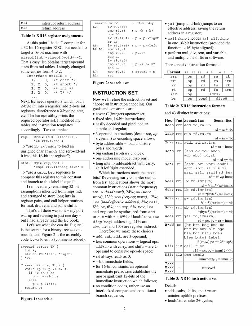
I copied xr16.md from mips.md, added it to the makefile, and added an xr16 target option. I designed xr16 register conventions (Table 1) and changed my md to target these registers.
Register Use r0 always zero r1 reserved for assembler r2 function return value r3-r5 function arguments r6-r9 temporaries r10-r12 register variables r13 stack pointer (sp)
2
r14 interrupt return address r15 return address
Table 1: XR16 register assignments
At this point I had a C compiler for a 32-bit 16-register RISC, but needed to target a 16-bit machine with sizeof(int)=sizeof(void*)=2. That�s easy: lcc obtains target operand sizes from md tables. I simply changed some entries from 4 to 2:
Interface xr16IR = {1, 1, 0, /* char */2, 2, 0, /* short */2, 2, 0, /* int */2, 2, 0, /* T* */...
Next, lcc needs operators which load a 2-byte int into a register, add 2-byte int registers, dereference a 2-byte pointer, etc. The lcc ops utility prints the required operator set. I modified my tables and instruction templates accordingly. Two examples:
reg: CVUI2(INDIRU1(addr)) \"lb r%c,%0\n" 1
⇒ �use lb rd,addr to load an unsigned char at addr and zero-extend it into this 16-bit int register�;
stmt: EQI2(reg,con) \"cmpi r%0,%1\nbeq %a\n" 2
⇒ �use a cmpi, beq sequence to compare this register to this constant and branch to this label if equal�.
I removed any remaining 32-bit assumptions inherited from mips.md, and arranged to store long ints in register pairs, and call helper routines for mul, div, rem, and some shifts.
That's all there was to it − my port was up and running in just one day − but I had already read the lcc book.
Let's see what she can do. Figure 1 is the source for a binary tree search routine, and Figure 2 is the assembly code lcc-xr16 emits (comments added).
typedef struct TN {int k;struct TN *left, *right;
} *T;
T search(int k, T p) {while (p && p->k != k)if (p->k < k)p = p->right;
elsep = p->left;
return p;}
Figure 1: search.c
_search:br L3 ; r3=k r4=pL2: lw r9,(r4)
cmp r9,r3 ; p->k < k?bge L5lw r4,4(r4) ; p = p->rightbr L6
L5: lw r4,2(r4) ; p = p->leftL6:L3: mov r9,r4
cmp r9,r0 ; p==0?beq L7lw r9,(r4)cmp r9,r3 ; p->k != k?bne L2
L7: mov r2,r4 ; retval = pL1: ret
Figure 2: search.asm
INSTRUCTION SET Now we'll refine the instruction set and choose an instruction encoding. Our goals and constraints are: • cover C (integer) operator set; • fixed size, 16-bit instructions; • easily decoded and pipelined ⇒
simple and regular; • 3-operand instructions (dest = src1 op
src2/imm) as encoding space allows; • byte addressable − load and store
bytes and words; • big endian (arbitrary choice); • one addressing mode, disp(reg); • long ints ⇒ add/subtract with carry,
shift left/right extended. Which instructions merit the most
bits? Reviewing early compiler output from test applications shows the most common instructions (static frequency) are lw (load word), 24%; sw (store word), 13%; mov (reg-reg move), 12%; lea (load effective address), 8%; call, 8%; br, 6%; and cmp, 6%. Mov, lea, and cmp can be synthesized from add or sub with r0. 69% of loads/stores use disp(reg) addressing, 21% are absolute, and 10% are register indirect.
Therefore we make these choices: • add, sub, addi are 3-operand; • less common operations − logical ops,
add/sub with carry, and shifts − are 2-operand to conserve opcode space;
• r0 always reads as 0; • 4-bit immediate fields; • for 16-bit constants, an optional
immediate prefix imm establishes the most-significant 12-bits of the immediate instruction which follows;
• no condition codes, rather use an interlocked compare and conditional branch sequence;
• jal (jump-and-link) jumps to an effective address, saving the return address in a register;
• call func encodes jal r15,func in one 16-bit instruction (provided the function is 16-byte aligned);
• perform mul, div, rem, and variable and multiple bit shifts in software.
There are six instruction formats:
Format 15 12 11 8 7 4 3 0
rrr op rd ra rbrri op rd ra immrr op rd fn rbri op rd fn immi12 op imm12br op cond disp8
Table 2: XR16 instruction formats
and 43 distinct instructions:
Hex Fmt Assembler Semantics 0dab rrr add rd,ra,rb
rd = ra + rb;1dab rrr sub rd,ra,rb
rd = ra � rb;2dai rri addi rd,ra,imm
rd = ra + imm;3d*b rr {and or xor andn
adc sbc} rd,rbrd = rd op rb;
4d*i ri {andi ori xori andniadci sbci slli slxisrai srli srxi} rd,imm
rd = rd op imm;5dai rri lw rd,imm(ra)
rd = *(int*)(ra+imm);6dai rri lb rd,imm(ra)
rd = *(byte*)(ra+imm);8dai rri sw rd,imm(ra)
*(int*)(ra+imm) = rd;9dai rri sb rd,imm(ra)
*(byte*)(ra+imm) = rd;Adai rri jal rd,imm(ra)
rd = pc, pc = ra + imm;B*dd br {br brn beq bne bc
bnc bv bnv blt bgeble bgt bltu bgeubleu bgtu} label
if (cond) pc += 2*disp8;Ciii i12 call func
r15 = pc, pc = imm12<<4;Diii i12 imm imm12
imm'next15:4 = imm12;7xxxExxxFxxx
−
reserved
Table 3: XR16 instruction set
Details: • adds, subs, shifts, and imm are
uninterruptible prefixes; • loads/stores take 2+ cycles;
3
• jump and branch-taken take 3 cycles (no branch delay slots).
• 4-bit imm field encodes: • int (-8..7): add/sub, logic, shifts; • unsigned (0..15): lb, sb; • unsigned word displacement
(0,2,�,30): lw, sw, jal, call; Some assembly instructions are formed from other machine instructions:
Assembly Maps to nop and r0,r0mov rd,ra add rd,ra,r0cmp ra,rb sub r0,ra,rbsubi rd,ra,im addi rd,ra,-imcmpi ra,im addi r0,ra,-imcom rd xori rd,-1lea rd,imm(ra) addi rd,ra,immlbs rd,imm(ra)(load-byte, sign-extending)
lb rd,imm(ra)xori rd,0x80subi rd,0x80
j addr jal r0,addrret jal r0,0(r15)
Table 4: Some pseudo-instructions
Note only signed char data use lbs.
ASSEMBLER I wrote a little multi-pass assembler to translate the lcc assembly output into an executable image.
The xr16 assembler reads one or more assembly files and emits an image file and a listing file. It has a simple structure. The lexical analyzer reads the source characters and recognizes tokens, such as the identifier _main. The parser scans the tokens on each line and recognizes instructions and operands, such as register names and effective address expressions. The symbol table remembers labels and their addresses, and a fixup table remembers symbolic references.
In pass one, the assembler parses each line. Labels are added to the symbol table. Each instruction expands into one or more machine instructions. If an operand refers to a label, we record a fixup to it.
In pass two, we check all branch fixups. If a branch displacement exceeds 128 words, we rewrite it using a jump. Since inserting a jump may make other branches far, we repeat until no far branches remain.
Next we evaluate fixups. For each one, we look up the target address and apply that to the fixup subject word
Lastly we emit the output files.
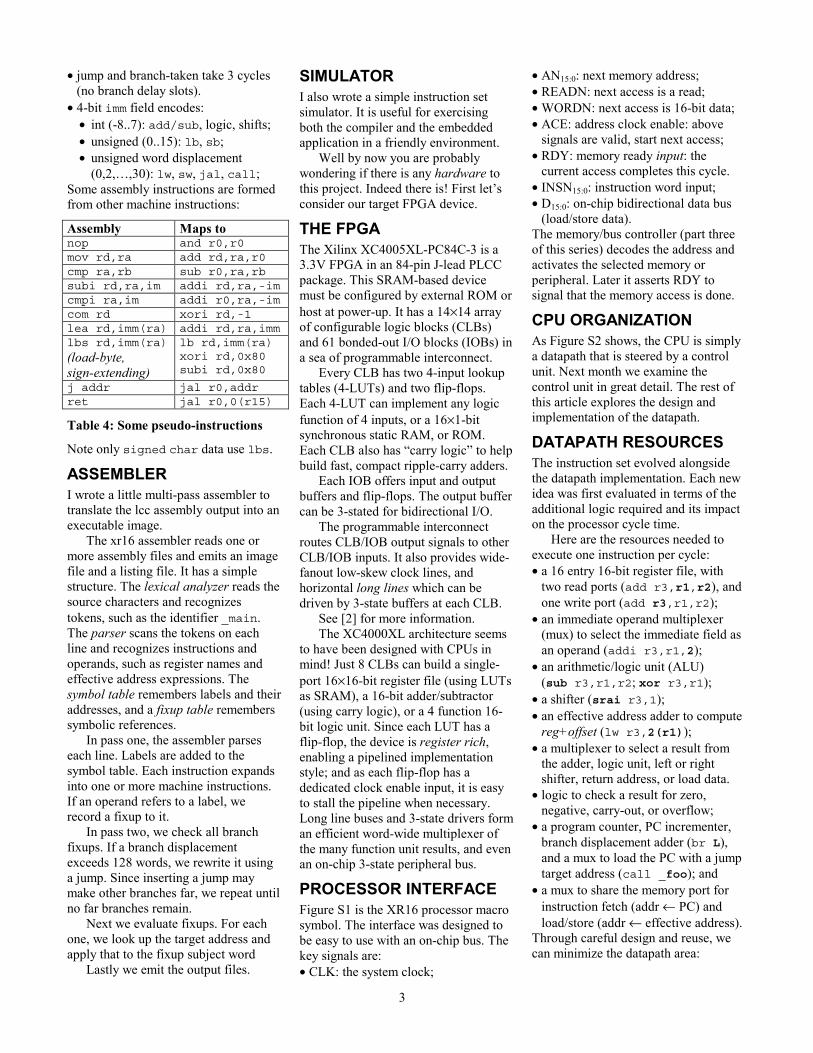
SIMULATOR I also wrote a simple instruction set simulator. It is useful for exercising both the compiler and the embedded application in a friendly environment.
Well by now you are probably wondering if there is any hardware to this project. Indeed there is! First let�s consider our target FPGA device.
THE FPGA The Xilinx XC4005XL-PC84C-3 is a 3.3V FPGA in an 84-pin J-lead PLCC package. This SRAM-based device must be configured by external ROM or host at power-up. It has a 14×14 array of configurable logic blocks (CLBs) and 61 bonded-out I/O blocks (IOBs) in a sea of programmable interconnect.
Every CLB has two 4-input lookup tables (4-LUTs) and two flip-flops. Each 4-LUT can implement any logic function of 4 inputs, or a 16×1-bit synchronous static RAM, or ROM. Each CLB also has �carry logic� to help build fast, compact ripple-carry adders.
Each IOB offers input and output buffers and flip-flops. The output buffer can be 3-stated for bidirectional I/O.
The programmable interconnect routes CLB/IOB output signals to other CLB/IOB inputs. It also provides wide-fanout low-skew clock lines, and horizontal long lines which can be driven by 3-state buffers at each CLB.
See [2] for more information. The XC4000XL architecture seems
to have been designed with CPUs in mind! Just 8 CLBs can build a single-port 16×16-bit register file (using LUTs as SRAM), a 16-bit adder/subtractor (using carry logic), or a 4 function 16-bit logic unit. Since each LUT has a flip-flop, the device is register rich, enabling a pipelined implementation style; and as each flip-flop has a dedicated clock enable input, it is easy to stall the pipeline when necessary. Long line buses and 3-state drivers form an efficient word-wide multiplexer of the many function unit results, and even an on-chip 3-state peripheral bus.
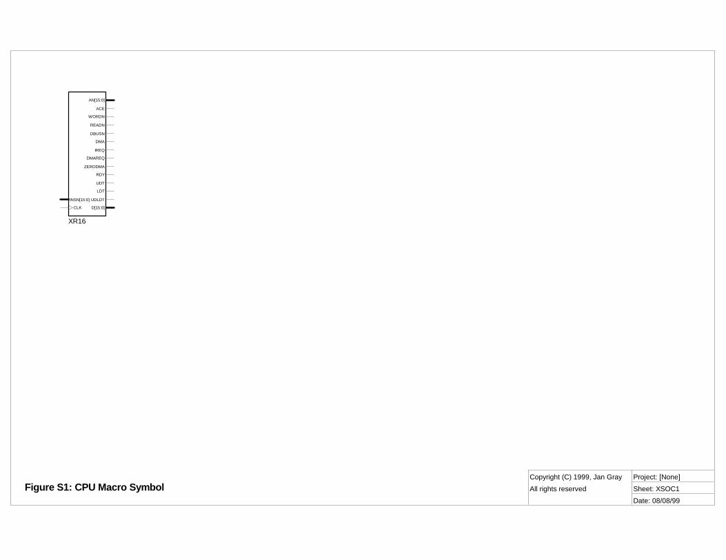
PROCESSOR INTERFACE Figure S1 is the XR16 processor macro symbol. The interface was designed to be easy to use with an on-chip bus. The key signals are: • CLK: the system clock;
• AN15:0: next memory address; • READN: next access is a read; • WORDN: next access is 16-bit data; • ACE: address clock enable: above
signals are valid, start next access; • RDY: memory ready input: the
current access completes this cycle. • INSN15:0: instruction word input; • D15:0: on-chip bidirectional data bus
(load/store data). The memory/bus controller (part three of this series) decodes the address and activates the selected memory or peripheral. Later it asserts RDY to signal that the memory access is done.
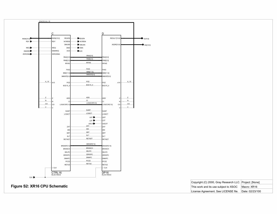
CPU ORGANIZATION As Figure S2 shows, the CPU is simply a datapath that is steered by a control unit. Next month we examine the control unit in great detail. The rest of this article explores the design and implementation of the datapath.
DATAPATH RESOURCES The instruction set evolved alongside the datapath implementation. Each new idea was first evaluated in terms of the additional logic required and its impact on the processor cycle time.
Here are the resources needed to execute one instruction per cycle: • a 16 entry 16-bit register file, with
two read ports (add r3,r1,r2), and one write port (add r3,r1,r2);
• an immediate operand multiplexer (mux) to select the immediate field as an operand (addi r3,r1,2);
• an arithmetic/logic unit (ALU) (sub r3,r1,r2; xor r3,r1);
• a shifter (srai r3,1); • an effective address adder to compute
reg+offset (lw r3,2(r1)); • a multiplexer to select a result from
the adder, logic unit, left or right shifter, return address, or load data.
• logic to check a result for zero, negative, carry-out, or overflow;
• a program counter, PC incrementer, branch displacement adder (br L), and a mux to load the PC with a jump target address (call _foo); and
• a mux to share the memory port for instruction fetch (addr ← PC) and load/store (addr ← effective address).
Through careful design and reuse, we can minimize the datapath area:
4
• the adder, with the immediate mux, can do the effective address add;
• the PC incrementer can also add branch displacements; and
• the memory address mux can help load the PC with the jump target.
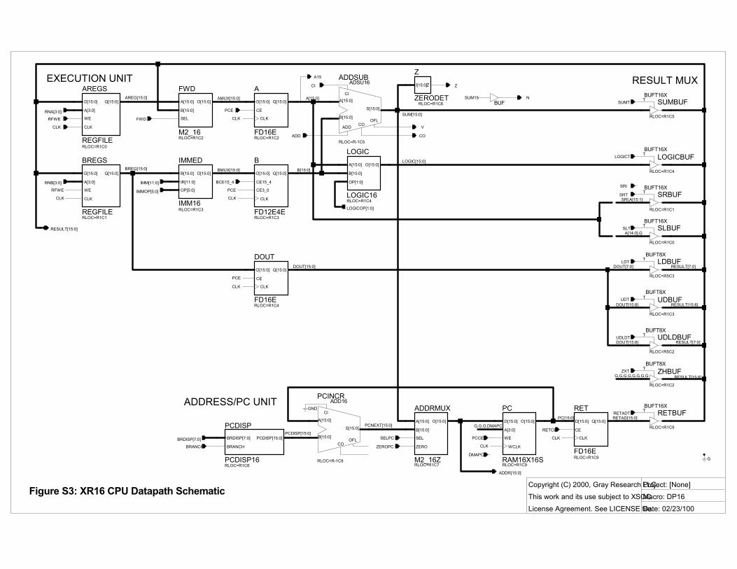
DATAPATH SCHEMATIC Figure S3, the datapath schematic, is the culmination of these ideas. There are three groups of resources:
Execution unit: the heart of the processor. Fetches operands from the register file and the immediate fields of the instruction register, presents them to the add/sub, logic, and (trivial) shift units, and writes back the result to the register file.
Result multiplexer: selects one result from the various function units.
Address/PC unit: drives the next memory address, and includes the PC, PC adder, and address mux.
Now let�s see how each resource is implemented in our FPGA.
REGISTER FILE Each cycle we must read two register operands and write back one result.
We get two read ports, AREG and BREG, by keeping two copies of the 16×16-bit register file REGFILE, and reading one operand from each. Each cycle we must write the same result value into both copies.
So for each REGFILE, each clock cycle we must do one read access and one write access.
Each REGFILE is a 16×16 RAM. Recall each CLB has two 4-LUTs, each of which can be a 16×1-bit RAM. Thus a REGFILE is a column of 8 CLBs. Each REGFILE also has an internal 16-bit output register that captures the RAM output on the CLK falling edge.
To read and write the REGFILE each clock, we double-cycle it.
In the first half of each clock cycle, the control unit presents a �read port� source operand register number to the RAM address inputs. The selected register is read out and captured in the REGFILE output register as CLK falls.
In the second half cycle, the control unit drives the �write port� register number. As CLK rises, the RESULT15:0 is written to the destination register.
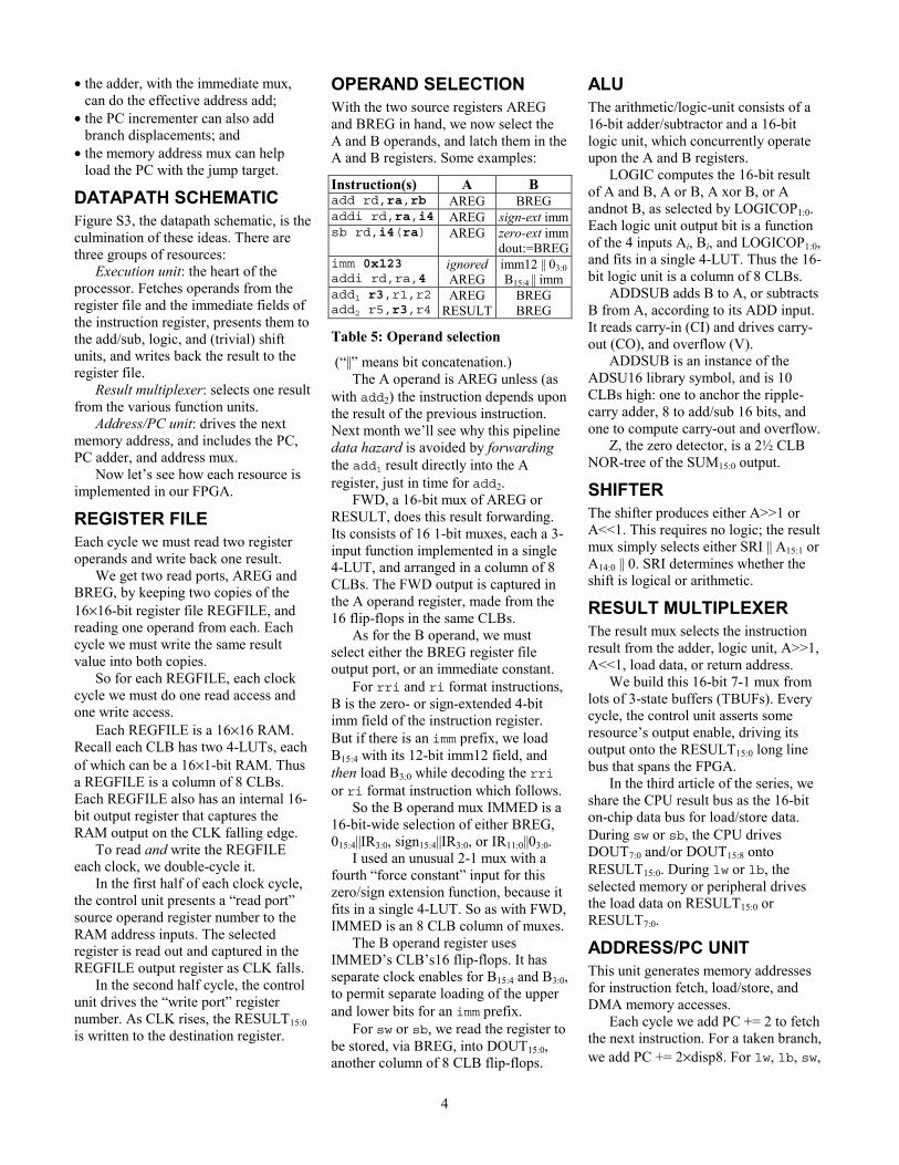
OPERAND SELECTION With the two source registers AREG and BREG in hand, we now select the A and B operands, and latch them in the A and B registers. Some examples:
Instruction(s) A B add rd,ra,rb AREG BREG addi rd,ra,i4 AREG sign-ext imm sb rd,i4(ra) AREG zero-ext imm
dout:=BREGimm 0x123addi rd,ra,4
ignored AREG
imm12 || 03:0 B15:4 || imm
add1 r3,r1,r2add2 r5,r3,r4
AREGRESULT
BREG BREG
Table 5: Operand selection
(�||� means bit concatenation.) The A operand is AREG unless (as
with add2) the instruction depends upon the result of the previous instruction. Next month we�ll see why this pipeline data hazard is avoided by forwarding the add1 result directly into the A register, just in time for add2.
FWD, a 16-bit mux of AREG or RESULT, does this result forwarding. Its consists of 16 1-bit muxes, each a 3-input function implemented in a single 4-LUT, and arranged in a column of 8 CLBs. The FWD output is captured in the A operand register, made from the 16 flip-flops in the same CLBs.
As for the B operand, we must select either the BREG register file output port, or an immediate constant.
For rri and ri format instructions, B is the zero- or sign-extended 4-bit imm field of the instruction register. But if there is an imm prefix, we load B15:4 with its 12-bit imm12 field, and then load B3:0 while decoding the rri or ri format instruction which follows.
So the B operand mux IMMED is a 16-bit-wide selection of either BREG, 015:4||IR3:0, sign15:4||IR3:0, or IR11:0||03:0.
I used an unusual 2-1 mux with a fourth �force constant� input for this zero/sign extension function, because it fits in a single 4-LUT. So as with FWD, IMMED is an 8 CLB column of muxes.
The B operand register uses IMMED�s CLB�s16 flip-flops. It has separate clock enables for B15:4 and B3:0, to permit separate loading of the upper and lower bits for an imm prefix.
For sw or sb, we read the register to be stored, via BREG, into DOUT15:0, another column of 8 CLB flip-flops.
ALU The arithmetic/logic-unit consists of a 16-bit adder/subtractor and a 16-bit logic unit, which concurrently operate upon the A and B registers.
LOGIC computes the 16-bit result of A and B, A or B, A xor B, or A andnot B, as selected by LOGICOP1:0. Each logic unit output bit is a function of the 4 inputs Ai, Bi, and LOGICOP1:0, and fits in a single 4-LUT. Thus the 16-bit logic unit is a column of 8 CLBs.
ADDSUB adds B to A, or subtracts B from A, according to its ADD input. It reads carry-in (CI) and drives carry-out (CO), and overflow (V).
ADDSUB is an instance of the ADSU16 library symbol, and is 10 CLBs high: one to anchor the ripple-carry adder, 8 to add/sub 16 bits, and one to compute carry-out and overflow.
Z, the zero detector, is a 2½ CLB NOR-tree of the SUM15:0 output.
SHIFTER The shifter produces either A>>1 or A<<1. This requires no logic; the result mux simply selects either SRI || A15:1 or A14:0 || 0. SRI determines whether the shift is logical or arithmetic.
RESULT MULTIPLEXER The result mux selects the instruction result from the adder, logic unit, A>>1, A<<1, load data, or return address.
We build this 16-bit 7-1 mux from lots of 3-state buffers (TBUFs). Every cycle, the control unit asserts some resource�s output enable, driving its output onto the RESULT15:0 long line bus that spans the FPGA.
In the third article of the series, we share the CPU result bus as the 16-bit on-chip data bus for load/store data. During sw or sb, the CPU drives DOUT7:0 and/or DOUT15:8 onto RESULT15:0. During lw or lb, the selected memory or peripheral drives the load data on RESULT15:0 or RESULT7:0.
ADDRESS/PC UNIT This unit generates memory addresses for instruction fetch, load/store, and DMA memory accesses.
Each cycle we add PC += 2 to fetch the next instruction. For a taken branch, we add PC += 2×disp8. For lw, lb, sw,
5
sb, jal, and call, we load PC with the effective address SUM from ADDSUB.
Refer to the Figure S3 to see how this works. PCINCR adds PC and the PCDISP mux output (either +2 or the branch displacement) giving PCNEXT. ADDRMUX selects PCNEXT or SUM as the next memory address.
When the next memory access is an instruction fetch, ADDR ← PCNEXT, and PCCE (PC clock enable) is asserted to update PC with PCNEXT.
When the next access is a load/store, SELPC and PCCE are false, and ADDR ← SUM, without updating PC.
PCDISP is a 16-bit mux of +215:0 and 2×disp8, 5 CLBs tall.
PCINCR is an instance of the ADD16 library symbol, 9 CLBs tall.
ADDRMUX is a 16-bit 2-1 mux with a fourth input, ZERO, to set PC to 0 on reset. It�s 16 LUTs, 8 CLBs tall.
PC is not a simple register, but rather a 16 entry register file. PC0 is the CPU PC, and PC1 is the DMA address. PC is a 16×16 RAM, 8 CLBs tall.
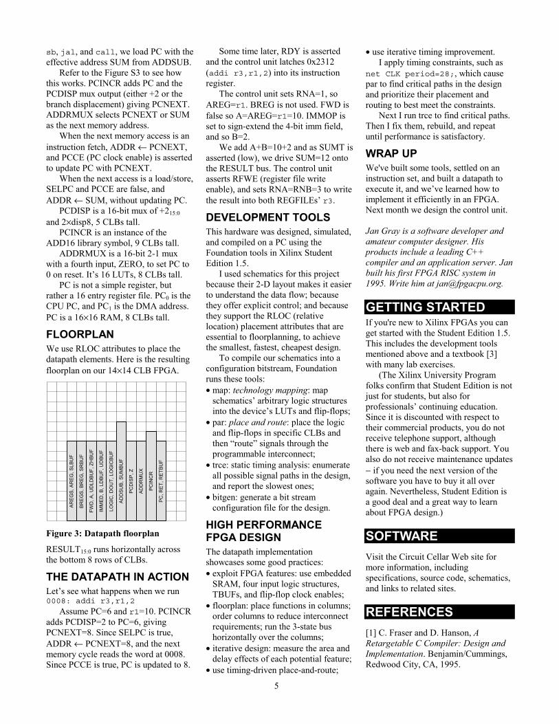
FLOORPLAN We use RLOC attributes to place the datapath elements. Here is the resulting floorplan on our 14×14 CLB FPGA.
AREG
S, A
REG
, SLB
UF
BREG
S, B
REG
, SR
BUF
FWD
, A, U
DLD
BUF,
ZH
BUF
IMM
ED, B
, LD
BUF,
UD
BUF
LOG
IC, D
OU
T, L
OG
ICBU
F
ADD
SUB,
SU
MBU
F
PCD
ISP,
Z
ADD
RM
UX
PCIN
CR
PC, R
ET, R
ETBU
F
Figure 3: Datapath floorplan
RESULT15:0 runs horizontally across the bottom 8 rows of CLBs.
THE DATAPATH IN ACTION Let�s see what happens when we run 0008: addi r3,r1,2
Assume PC=6 and r1=10. PCINCR adds PCDISP=2 to PC=6, giving PCNEXT=8. Since SELPC is true, ADDR ← PCNEXT=8, and the next memory cycle reads the word at 0008. Since PCCE is true, PC is updated to 8.
Some time later, RDY is asserted and the control unit latches 0x2312 (addi r3,r1,2) into its instruction register.
The control unit sets RNA=1, so AREG=r1. BREG is not used. FWD is false so A=AREG=r1=10. IMMOP is set to sign-extend the 4-bit imm field, and so B=2.
We add A+B=10+2 and as SUMT is asserted (low), we drive SUM=12 onto the RESULT bus. The control unit asserts RFWE (register file write enable), and sets RNA=RNB=3 to write the result into both REGFILEs� r3.
DEVELOPMENT TOOLS This hardware was designed, simulated, and compiled on a PC using the Foundation tools in Xilinx Student Edition 1.5.
I used schematics for this project because their 2-D layout makes it easier to understand the data flow; because they offer explicit control; and because they support the RLOC (relative location) placement attributes that are essential to floorplanning, to achieve the smallest, fastest, cheapest design.
To compile our schematics into a configuration bitstream, Foundation runs these tools: • map: technology mapping: map
schematics� arbitrary logic structures into the device�s LUTs and flip-flops;
• par: place and route: place the logic and flip-flops in specific CLBs and then �route� signals through the programmable interconnect;
• trce: static timing analysis: enumerate all possible signal paths in the design, and report the slowest ones;
• bitgen: generate a bit stream configuration file for the design.
HIGH PERFORMANCE FPGA DESIGN The datapath implementation showcases some good practices: • exploit FPGA features: use embedded
SRAM, four input logic structures, TBUFs, and flip-flop clock enables;
• floorplan: place functions in columns; order columns to reduce interconnect requirements; run the 3-state bus horizontally over the columns;
• iterative design: measure the area and delay effects of each potential feature;
• use timing-driven place-and-route;
• use iterative timing improvement. I apply timing constraints, such as
net CLK period=28;, which cause par to find critical paths in the design and prioritize their placement and routing to best meet the constraints.
Next I run trce to find critical paths. Then I fix them, rebuild, and repeat until performance is satisfactory.
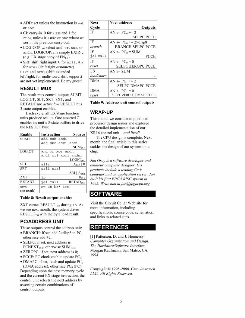
WRAP UP We've built some tools, settled on an instruction set, and built a datapath to execute it, and we�ve learned how to implement it efficiently in an FPGA. Next month we design the control unit. Jan Gray is a software developer and amateur computer designer. His products include a leading C++ compiler and an application server. Jan built his first FPGA RISC system in 1995. Write him at [email protected].
GETTING STARTED If you're new to Xilinx FPGAs you can get started with the Student Edition 1.5. This includes the development tools mentioned above and a textbook [3] with many lab exercises.
(The Xilinx University Program folks confirm that Student Edition is not just for students, but also for professionals� continuing education. Since it is discounted with respect to their commercial products, you do not receive telephone support, although there is web and fax-back support. You also do not receive maintenance updates − if you need the next version of the software you have to buy it all over again. Nevertheless, Student Edition is a good deal and a great way to learn about FPGA design.)
SOFTWARE Visit the Circuit Cellar Web site for more information, including specifications, source code, schematics, and links to related sites.
REFERENCES [1] C. Fraser and D. Hanson, A Retargetable C Compiler: Design and Implementation. Benjamin/Cummings, Redwood City, CA, 1995.
6
[2] T. Cantrell, "VolksArray," Circuit Cellar Ink, April 1998, pp. 82-86.
[3] D. Van den Bout, The Practical Xilinx® Designer Lab Book, Prentice Hall, 1998. (Available separately and included with Xilinx Student Edition.)
SOURCES Xilinx Student Edition 1.5 www.amazon.com/exec/obidos/ASIN/0130205869
Xilinx FPGAs www.xilinx.com/products/sp_xl.htm, .../xc4000XLA.html
Copyright © 1998-2000, Gray Research LLC. All Rights Reserved.
Copyright (C) 1999, Jan GrayAll rights reserved
Project: [None]Sheet: XSOC1Date: 08/08/99
Figure S1: CPU Macro Symbol
XR16
CLK
ACE
AN[15:0]
RDY
READN
WORDN
D[15:0]
UDT
LDT
INSN[15:0]
DMA
UDLDT
DBUSN
IREQ
DMAREQ
ZERODMA
Copyright (C) 2000, Gray Research LLC.This work and its use subject to XSOCLicense Agreement. See LICENSE file.
Project: [None]Macro: XR16Date: 02/23/100
Figure S2: XR16 CPU Schematic
D
DP16RLOC=R5C0
BRDISP[7:0]
LOGICOP[1:0]
RNA[3:0]
RNB[3:0]
PCE
ADD
BCE15_4
BRANCH
CI
IMMOP[5:0]
A15
LOGICT
RETADT
RFWE
SELPC
SLT
SRT
SRI
SUMT
ZXT
ZEROPC
CLK
Z
ADDR[15:0]
RESULT[15:0]
CO
V
N
FWD
IMM[11:0]
LDT
UDT
UDLDT
DMAPC
PCCE
RETCE
C
CTRL16RLOC=R0C0
A15
Z
N
V
RNA[3:0]
RNB[3:0]
RFWE
IMMOP[5:0]
PCE
BCE15_4
ADD
CI
LOGICOP[1:0]
SUMT
LOGICT
ZXT
SRT
SLT
RETADT
CLK
SELPC
ZEROPC
ACE
SRI
FWD
CO
RDY
IMM[11:0]
READN
WORDN
INSN[15:0]
BRDISP[7:0]
BRANCH
DMA
DBUSN
DMAPC
PCCE
RETCE
IREQ
DMAREQ
ZERODMARNA[3:0]
RNB[3:0]
IMM[11:0]
LOGICOP[1:0]
Z,N,CO,V,A_15
AN[15:0]
BRDISP[7:0]
IMMOP[5:0]
D[15:0]INSN[15:0]
CLK
BRANCH
RFWE
FWD
PCE
BCE15_4
SELPC
ZEROPC
ADD
CI
SUMT
LOGICT
DMA
N
CO
ZXT
SRI
SRT
SLT
RETADT
RDY WORDN
UDLDT
V
A_15A_15
Z
N
CO
V
READN
Z
UDT
LDT
ACE
ZERODMA
DMAPC
PCCE
RETCE
IREQ
DMAREQ
DBUSN
Copyright (C) 2000, Gray Research LLC.This work and its use subject to XSOCLicense Agreement. See LICENSE file.
Project: [None]Macro: DP16Date: 02/23/100
EXECUTION UNIT
ADDRESS/PC UNIT
RESULT MUX
Figure S3: XR16 CPU Datapath Schematic
RETBUF
RLOC=R1C9
BUFT16XT
BREGS
REGFILERLOC=R1C1
D[15:0]
A[3:0]
WE
CLK
Q[15:0]
LOGICBUF
RLOC=R1C4
BUFT16XT
SRBUF
RLOC=R1C1
BUFT16XT
IMMED
IMM16RLOC=R1C3
B[15:0]
IR[11:0]
O[15:0]
OP[5:0]
B
FD12E4ERLOC=R1C3
D[15:0] Q[15:0]
CE15_4
CE3_0
CLK
AREGS
REGFILERLOC=R1C0
D[15:0]
A[3:0]
WE
CLK
Q[15:0]
A
FD16ERLOC=R1C2
D[15:0]
CE
CLK
Q[15:0]
ADDSUB
RLOC=R-1C5
ADSU16
A[15:0]
ADD
B[15:0]
CI
COOFL
S[15:0]
LOGIC
LOGIC16RLOC=R1C4
A[15:0]
B[15:0]
OP[1:0]
O[15:0]
SUMBUF
RLOC=R1C5
BUFT16XTBUF
SLBUF
RLOC=R1C0
BUFT16XT
PCINCR
RLOC=R-1C8
ADD16
A[15:0]
B[15:0]
CI
COOFL
S[15:0]
ADDRMUX
M2_16ZRLOC=R1C7
A[15:0]
B[15:0]
SEL
O[15:0]
ZERO
PC
RAM16X16SRLOC=R1C9
A[3:0]
D[15:0]
WE
WCLK
O[15:0]
RET
FD16ERLOC=R1C9
D[15:0]
CE
CLK
Q[15:0]PCDISP
PCDISP16RLOC=R1C6
BRDISP[7:0]
BRANCH
PCDISP[15:0]
ZHBUF
RLOC=R1C2
BUFT8XT
DOUT
FD16ERLOC=R1C4
D[15:0]
CE
CLK
Q[15:0]
FWD
M2_16RLOC=R1C2
A[15:0]
B[15:0]
SEL
O[15:0]
Z
ZERODETRLOC=R1C6
I[15:0]Z
UDLDBUF
RLOC=R5C2
BUFT8XT
UDBUF
RLOC=R1C3
BUFT8XT
LDBUF
RLOC=R5C3
BUFT8XT
RNA[3:0]
RNB[3:0]
AREG[15:0]
BREG[15:0] B[15:0]
AMUX[15:0]
BMUX[15:0]
RETAD[15:0]
A[15:0]
SUM[15:0]
LOGIC[15:0]
PCNEXT[15:0]
IMMOP[5:0]
PCDISP[15:0]
IMM[11:0]
DOUT[7:0]
BRDISP[7:0]
G,G,G,G,G,G,G,G
RESULT[15:8]
RESULT[15:8]
SRI,A[15:1]
RESULT[7:0]
RESULT[15:0]
PC[15:0]
DOUT[15:8] RESULT[7:0]
DOUT[15:8]
LOGICOP[1:0]
DOUT[15:0]
A[14:0],G
ADDR[15:0]
G,G,G,DMAPC
CLK
RFWE
ZXT
CLK
CLK
RFWE
CLK
PCE
SLT
Z
RETADT
PCCE
LDT
GND
SRT
SUMT
LOGICT
CI
ADD
FWD
N
A15
CLK
CO
SELPC
ZEROPC
CLK
CLK
BCE15_4
V
G
SUM15
PCE
BRANCH
PCESRI
UDLDT
UDT
RETCE
DMAPC
1
Building a RISC CPU and System-on-a-Chip in an FPGA
Pipeline and Control Unit Design
Jan Gray, Gray Research LLC FINAL DRAFT: 10/15/1999
Part 2 of 3. Jan builds a pipelined 16-bit RISC processor and system-on-a-chip in an FPGA. This month he explores the CPU pipeline and designs the control unit.
LAST MONTH we discussed the instruction set and the datapath of our XR16 16-bit RISC processor. Now we�ll design the control unit that pushes the datapath�s buttons.
Figure S2 (last month) shows the CTRL16 control unit schematic symbol in context. Inputs include the RDY signal from the memory controller, the next instruction word INSN15:0 from memory, and the zero, negative, carry, and overflow outputs from the datapath.
The control unit outputs manage the datapath. These include pipeline control clock enables, register and operand selectors, ALU controls, and result multiplexer output enables.
Before we design the control circuitry, we first consider how the pipeline behaves in good times and bad.
PIPELINED EXECUTION To increase instruction throughput, the XR16 has a three stage pipeline: instruction fetch (IF), decode and operand fetch (DC), and execute (EX).
In the IF stage, we read memory at the current PC address, capture the resulting instruction word in the instruction register IR, and increment PC for the next cycle.
In the DC stage, the instruction is decoded and its operands are read from the register file or extracted from an immediate field in the IR.
In the EX stage, the function units act upon the operands. One result is driven through 3-state buffers onto the result bus, and is written back into the register file as the cycle ends.
Consider executing a series of instructions and assume no memory wait states. Every pipeline cycle we
fetch a new instruction and write back its result two cycles later. In each cycle we simultaneously prepare next instruction address PC+2, fetch instruction IPC, decode instruction IPC-2, and execute instruction IPC-4.
t1 t2 t3 t4 t5 IF1 DC1 EX1
IF2 DC2 EX2 IF3 DC3 EX3 IF4 DC4
Table 1: Pipelined execution
Here the processor fetches instruction I1 at time t1 and computes its result in t3, while I2 starts in t2 and ends in t4. Memory accesses are in boldface.
That�s the simple case. But there are several pipeline complications to consider: data hazards, memory wait states, load/store instructions, jumps and branches, interrupts, and DMA.
DATA HAZARDS AND RESULT FORWARDING What happens when an instruction uses the result of the preceding instruction?
I1: andi r1,7I2: add r2,r1,1
Figure 1: I1 result r1 used In I2
Referring back to time t3 of Table 1, EX1 computes r1=r1&7 while DC2 fetches the old value of r1. In t4 EX2 adds 1 to this old r1. Oops!
This is a data hazard and there are several ways to address it. The assembler can reorder instructions or insert nops to avoid the problem. Or the control unit can detect the hazard and stall the pipeline one cycle in order to
2
write-back the result to the register file before fetching it as a source register. But these techniques hurt performance.
Instead, we do result forwarding, also known as register file bypass. The datapath DC stage includes FWD, a 16-bit 2-1 multiplexer (mux) of AREG (register file port A) and the result bus. Most of the time, FWD passes AREG to the A operand register. But when the control unit detects the hazard (DC source register equals EX destination register), it asserts its FWD output signal, and the A register receives the I1 result, just in time for EX2 in t4.
Unlike most pipelined CPUs, the XR16 only forwards results to the A operand � a speed/area tradeoff. The assembler handles any rare port B data hazards by swapping A and B operands if possible, inserting nops if not.
MEMORY INTERFACE The processor has a single memory port to read instructions and to load and store data. Most memory accesses are to fetch instructions. The processor is also the DMA engine, and a video refresh DMA cycle occurs once every eight clocks or so.
So in any given clock cycle, the processor executes either an instruction fetch memory cycle, a DMA memory cycle, or a load/store memory cycle.
Memory transactions are pipelined. Each memory cycle, the processor drives the next memory cycle�s address and control signals and awaits RDY, indicating the access has completed.
WAIT! So what happens when memory is not ready? The simplest thing to do is to stop the pipeline for that cycle. CTRL deasserts all pipeline register clock enables PCE, ACE, etc. The pipeline registers do not clock, and this extends all pipeline stages by one cycle.
In the following example, memory is not ready during the fetch of instruction I3 in t3 and so t4 repeats t3. Repeated pipe stages are italicized.
t1 t2 t3 t4 t5 IF1 DC1 EX1 EX1
IF2 DC2 DC2 EX2 IF3 IF3 DC3 IF4
Table 2: IF3 memory not ready at t3
LOADS AND STORES Loads and stores need a second memory access � pipeline havoc! Scenario:
if ((p->flags & 7) == 1)p->x = p->y;
IL: lw r6,2(r10)I2: andi r6,7I3: addi r0,r6,-1IB: bne TI5: lw r6,6(r10)
...
Figure 2: Load instruction in situ
Its pipelined execution:
t1 t2 t3 t4 t5 IFL DCL EXL EXL
IF2 DC2 DC2 EX2 IF3 IF3 DC3 IFB
Table 3: Pipelined load execution
There are several gotchas here. 1. In t4 we run a load/store memory
cycle instead of an instruction fetch. We must stall the pipeline to squeeze in this access.
2. Although we fetched I3 in t3, we must not latch it into the instruction register IR as t3 ends, because neither EXL nor DC2 are finished yet. In particular, DC2 must await the load result in order to forward it to A, because I2 uses r6, the result of IL!
3. If, in t3, we don�t save the just-fetched I3 somewhere, we�ll lose it, because in t4 the memory port is busy with the load cycle. If we lose it, we�ll have to re-fetch it, no sooner than t5, with the result that even a no-wait load requires three cycles � unacceptable.
To fix this problem, we provide a 16-bit NEXTIR register and an IR source multiplexer IRMUX. In t3 we capture I3 in NEXTIR, and then in t4 IR is loaded from NEXTIR instead of from the memory port (which is busy with the load). For this 8 CLB overhead, we ensure 2-cycle loads and stores.
WAIT! WAIT! Let�s combine the last two topics, and consider how the pipeline for the code in Fig. 2 might proceed if the memory cycles for the instruction fetch IF3 and the load EXL each require two clocks, e.g. one wait state RAM. We�ll start at clock t3.
t3 t4 t5 t6 t7 EXL EXL EXL EXL DC2 DC2 DC2 DC2 EX2 IF3 IF3 IF3 IF3 DC3
IFB
Table 4: Fetch, load with wait states
This is fairly straightforward: RDY is not asserted during t3 and t5 so we repeat these cycles in t4 and t6.
JUMPS AND BRANCHES Next consider the effect of jumps (call and jal) and taken branches. By the time we execute the jump or taken branch IJ during EXJ, updating PC, we will have decoded IJ+1 and fetched IJ+2. These instructions in the branch shadow, and their side effects, must be annulled.
Continuing the Table 3 example from time t5, and assuming the branch is taken at t7, we must annul the EX5 stage of I5 and the DC6 and EX6 stages of I6. (Annulled stages are struck through.) Execution continues at instruction IT:
t5 t6 t7 t8 t9 EX2 DC3 EX3 IFB DCB EXB
IF5 DC5 EX5 IF6 DC6 EX6 IFT DCT
Table 5: Branch shadow annulled
T9 is not an EX5 load cycle because the I5 load is annulled.
Since we always annul the two branch shadow instructions, jumps and taken branches take 3 cycles.
Jumps also save the return address in the destination register. This return address is obtained from the RET register, which holds the address of the instruction in the DC pipeline stage.
INTERRUPTS When an interrupt request occurs, we must somehow jump to the interrupt handler, preserve the interrupt return address, retire the current pipeline, execute the handler, and later, return to the interrupted instruction.
We do this in a very simple way. (Thank goodness we have no branch delay slots or condition codes!) When INTREQ is asserted, we override the fetched instruction with int, e.g. jal r14,10(r0), via the IRMUX.
3
This jumps to the interrupt handler at 0x0010 and leaves the return address in r14, reserved for this purpose.
When the handler completes, it executes iret, e.g. jal r0,0(r14), and execution resumes with the interrupted instruction.
There are two pipeline issues. 1. We must not interrupt an
interlocked instruction sequence, e.g. any add, sub, shift, or imm followed by another instruction. If an interlocked instruction is in the DC stage, the interrupt is deferred one cycle.
2. The int must not be inserted in a branch or jump shadow, lest it be annulled. If a branch or jump is in the DC stage, or if a taken branch or jump is in the EX stage, the interrupt is deferred.
The simplicity pays off. The time to take an interrupt and then return from a null interrupt handler is only 6 cycles.
You might be wondering, �what about interrupt priorities, non-maskable interrupts, nested interrupts, interrupt vectors?� These artifacts of the fixed-pinout era need not be hardwired into our FPGA CPU. They are best done by collaboration with an on-chip interrupt controller and the interrupt handler.
DMA The last pipeline issue is peripheral direct memory access (DMA). The PC/address unit doubles as a DMA engine. Using a 16×16 RAM as a PC register file, we can fetch either an instruction (AN ← PC0 += 2) or a DMA word (AN ← PC1 += 2) per memory cycle.
After an instruction is fetched, if DMAREQ has been asserted, we insert one DMA memory cycle. (One suffices for this project.)
This PC register file costs 8 CLBs for the RAM, but saves 16 CLBs otherwise necessary for a separate 16-bit DMA address counter and a 16-bit 2-1 address mux, and shaves a couple of nanoseconds from the system�s critical path. It�s a nice example of a problem specific optimization you can build with a customizable processor.
CYCLES OF CYCLES To recap,
Each instruction takes three pipeline cycles, to move through the instruction
fetch, operand fetch and decode, and execute pipeline stages.
Each pipeline cycle requires up to three memory access cycles (mandatory instruction fetch, optional DMA, optional EX stage load or store).
Each memory access cycle requires one or more clock cycles.
ON TO THE DESIGN Now that we understand the pipeline, we are ready to design the control unit. (Lost? Learn all about pipelines in [1].)
First, here are some important naming conventions. Some control unit signal names have prefixes and suffixes to recognize their function or context. • Nsig: not signal � signal inverted; • DCsig: a DC stage signal; • EXsig: an EX stage signal; • sigN: signal in �next cycle� � input to
a flip-flop whose output is sig; • sigCE: flip-flop clock enable; • sigT: active low 3-state buffer output
enable. Most signal names sans prefix are
DC stage signals.
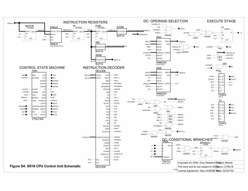
THE CONTROL UNIT Figure S4 is the control unit schematic, the implementation of CTRL16 of Figure S2. The control unit consists of: • the control finite state machine; • the instruction registers (next, decode
stage, execute stage); • the instruction decoder; • decode stage operand selection logic
(register file, forwarding, and immediate operand control);
• execute stage logic (ALU and result mux control); and
• conditional branch control. Here�s how an instruction flows
through the control unit pipeline: IF stage: When the instruction fetch
read completes, the new instruction at INSN15:0 is latched into IR.
DC stage: DECODE decodes IR to derive internal control signals. In the first half clock cycle, CTRL drives RNA3:0 and RNB3:0 with the source registers to read, and drives FWD and IMM5:0 to select the A and B operands. If the instruction is a branch, CTRL determines if it is taken. Then as the pipeline advances, the instruction passes into EXIR.
EX stage: Now CTRL drives ALU and result mux controls. If the
instruction is a load/store, it inserts a memory access. In the last half cycle, RNA and RNB both drive the destination register number, to store the result into the register file.
Now we�ll consider each part of the control unit in more detail.
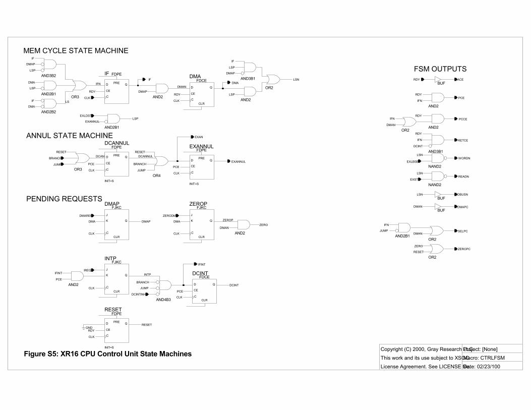
FINITE STATE MACHINE The control FSM has three states: • IF: current memory access is an
instruction fetch cycle; • DMA: current access is a DMA cycle; • LS: current access is a load/store. Here�s the state transition diagram:
IF
DMA
LS
DMAP*LSP
DMAP*LSP
DMAP
LSP
LSP
DMAP: DMA pendingLSP: load/store pending
Figure 3: Control unit FSM
Each memory cycle is an instruction fetch unless there is a DMA transfer pending or the EX stage instruction is a load or store.
The FSM clocks when one memory transaction completes and another begins (on RDY).
CTRLFSM also has several other bits of state: • DCANNUL: annul DC stage; • EXANNUL: annul EX stage; • DCINT: int in DC stage; • DMAP: DMA transfer pending; • INTP: interrupt pending.
DCANNUL and EXANNUL are set after executing a jump or taken branch. They suppress any effects of the two instructions in the branch shadow, including register file write-back and load/store memory accesses. So an annulled add still fetches and adds its operands, but its results are not retired to the register file.
DCINT is set in the pipeline cycle following the insertion of the int instruction. It inhibits clocking of RET for one cycle, so that the int picks up the return address of the interrupted instruction rather than the instruction after that.
4
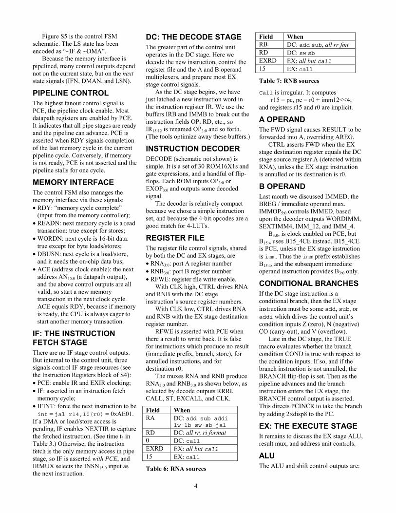
Figure S5 is the control FSM schematic. The LS state has been encoded as �~IF & ~DMA�.
Because the memory interface is pipelined, many control outputs depend not on the current state, but on the next state signals (IFN, DMAN, and LSN).
PIPELINE CONTROL The highest fanout control signal is PCE, the pipeline clock enable. Most datapath registers are enabled by PCE. It indicates that all pipe stages are ready and the pipeline can advance. PCE is asserted when RDY signals completion of the last memory cycle in the current pipeline cycle. Conversely, if memory is not ready, PCE is not asserted and the pipeline stalls for one cycle.
MEMORY INTERFACE The control FSM also manages the memory interface via these signals: • RDY: �memory cycle complete�
(input from the memory controller); • READN: next memory cycle is a read
transaction: true except for stores; • WORDN: next cycle is 16-bit data:
true except for byte loads/stores; • DBUSN: next cycle is a load/store,
and it needs the on-chip data bus; • ACE (address clock enable): the next
address AN15:0 (a datapath output), and the above control outputs are all valid, so start a new memory transaction in the next clock cycle. ACE equals RDY, because if memory is ready, the CPU is always eager to start another memory transaction.
IF: THE INSTRUCTION FETCH STAGE There are no IF stage control outputs. But internal to the control unit, three signals control IF stage resources (see the Instruction Registers block of S4): • PCE: enable IR and EXIR clocking; • IF: asserted in an instruction fetch
memory cycle; • IFINT: force the next instruction to be int = jal r14,10(r0) = 0xAE01.
If a DMA or load/store access is pending, IF enables NEXTIR to capture the fetched instruction. (See time t3 in Table 3.) Otherwise, the instruction fetch is the only memory access in pipe stage, so IF is asserted with PCE, and IRMUX selects the INSN15:0 input as the next instruction.
DC: THE DECODE STAGE The greater part of the control unit operates in the DC stage. Here we decode the new instruction, control the register file and the A and B operand multiplexers, and prepare most EX stage control signals.
As the DC stage begins, we have just latched a new instruction word in the instruction register IR. We use the buffers IRB and IMMB to break out the instruction fields OP, RD, etc., so IR15:12 is renamed OP3:0 and so forth. (The tools optimize away these buffers.)
INSTRUCTION DECODER DECODE (schematic not shown) is simple. It is a set of 30 ROM16X1s and gate expressions, and a handful of flip-flops. Each ROM inputs OP3:0 or EXOP3:0 and outputs some decoded signal.
The decoder is relatively compact because we chose a simple instruction set, and because the 4-bit opcodes are a good match for 4-LUTs.
REGISTER FILE The register file control signals, shared by both the DC and EX stages, are • RNA3:0: port A register number • RNB3:0: port B register number • RFWE: register file write enable.
With CLK high, CTRL drives RNA and RNB with the DC stage instruction�s source register numbers.
With CLK low, CTRL drives RNA and RNB with the EX stage destination register number.
RFWE is asserted with PCE when there a result to write back. It is false for instructions which produce no result (immediate prefix, branch, store), for annulled instructions, and for destination r0.
The muxes RNA and RNB produce RNA3:0 and RNB3:0 as shown below, as selected by decode outputs RRRI, CALL, ST, EXCALL, and CLK.
Field When RA DC: add sub addi
lw lb sw sb jal RD DC: all rr, ri format 0 DC: call EXRD EX: all but call 15 EX: call
Table 6: RNA sources
Field When RB DC: add sub, all rr fmt RD DC: sw sb EXRD EX: all but call 15 EX: call
Table 7: RNB sources
Call is irregular. It computes r15 = pc, pc = r0 + imm12<<4;
and registers r15 and r0 are implicit.
A OPERAND The FWD signal causes RESULT to be forwarded into A, overriding AREG.
CTRL asserts FWD when the EX stage destination register equals the DC stage source register A (detected within RNA), unless the EX stage instruction is annulled or its destination is r0.
B OPERAND Last month we discussed IMMED, the BREG / immediate operand mux. IMMOP5:0 controls IMMED, based upon the decoder outputs WORDIMM, SEXTIMM4, IMM_12, and IMM_4.
B3:0, is clock enabled on PCE, but B15:4 uses B15_4CE instead. B15_4CE is PCE, unless the EX stage instruction is imm. Thus the imm prefix establishes B15:4, and the subsequent immediate operand instruction provides B3:0 only.
CONDITIONAL BRANCHES If the DC stage instruction is a conditional branch, then the EX stage instruction must be some add, sub, or addi which drives the control unit�s condition inputs Z (zero), N (negative) CO (carry-out), and V (overflow).
Late in the DC stage, the TRUE macro evaluates whether the branch condition COND is true with respect to the condition inputs. If so, and if the branch instruction is not annulled, the BRANCH flip-flop is set. Then as the pipeline advances and the branch instruction enters the EX stage, the BRANCH control output is asserted. This directs PCINCR to take the branch by adding 2×disp8 to the PC.
EX: THE EXECUTE STAGE It remains to discuss the EX stage ALU, result mux, and address unit controls.
ALU The ALU and shift control outputs are:
5
• ADD: set unless the instruction is sub or sbc.
• CI: carry-in. 0 for adds and 1 for subs, unless it�s adc or sbc where we xor in the previous carry-out.
• LOGICOP1:0: select and, or, xor, or andn. LOGICOP1:0 is simply EXIR5:4 (e.g. EX stage copy of FN1:0).
• SRI: shift right input: 0 for srli, A15 for srai (shift right arithmetic).
Slxi and srxi (shift extended left/right, for multi-word shift support) are not yet implemented. Be my guest!
RESULT MUX The result mux control outputs SUMT, LOGICT, SLT, SRT, SXT, and RETADT are active low RESULT bus 3-state output enables.
Each cycle, all EX stage function units produce results. One asserted T enables its unit�s 3-state buffers to drive the RESULT bus:
Enable Instruction Source SUMT add sub addi
adc sbc adci sbci SUM15:0
LOGICT and or xor andnandi ori xori andni LOGIC15:0
SLT slli A14:0 || 0 SRT srli srai
SRI || A15:1ZXT lb 015:8 RETADT jal call RETAD15:0 none (no result)
sw sb br* imm �
Table 8: Result output enables
ZXT zeroes RESULT15:8 during lb. As we see next month, the system drives RESULT7:0 with the byte load result.
PC/ADDRESS UNIT These outputs control the address unit: • BRANCH: if set, add 2×disp8 to PC,
otherwise add +2. • SELPC: if set, next address is
PCNEXT15:0, otherwise SUM15:0. • ZEROPC: if set, next address is 0; • PCCE: PC clock enable: update PCi; • DMAPC: if set, fetch and update PC1
(DMA address), otherwise PC0 (PC). Depending upon the next memory cycle and the current EX stage instruction, the control unit selects the next address by asserting certain combinations of control outputs:
Next Cycle
Next address Outputs
IF AN ← PC0 += 2 SELPC PCCE
IF branch
AN ← PC0 += 2×disp8 BRANCH SELPC PCCE
IF jal call
AN ← PC0 = SUM PCCE
IF reset
AN ← PC0 = 0 SELPC ZEROPC PCCE
LS load/store
AN ← SUM -
DMA AN ← PC1 += 2 SELPC DMAPC PCCE
DMA reset
AN ← PC1 = 0 SELPC ZEROPC DMAPC PCCE
Table 9: Address unit control outputs
WRAP-UP This month we considered pipelined processor design issues and explored the detailed implementation of our XR16 control unit − and lived!
The CPU design is complete. Next month, the final article in this series tackles the design of our system-on-a-chip. Jan Gray is a software developer and amateur computer designer. His products include a leading C++ compiler and an application server. Jan built his first FPGA RISC system in 1995. Write him at [email protected].
SOFTWARE Visit the Circuit Cellar Web site for more information, including specifications, source code, schematics, and links to related sites.
REFERENCES [1] Patterson, D. and J. Hennessy, Computer Organization and Design: The Hardware/Software Interface, Morgan Kaufmann, San Mateo, CA, 1994.
Copyright © 1998-2000, Gray Research LLC. All Rights Reserved.
Copyright (C) 2000, Gray Research LLC.This work and its use subject to XSOCLicense Agreement. See LICENSE file.
Project: [None]Macro: CTRL16Date: 02/23/100
"N.C."
"N.C.""N.C."
"N.C."
INSTRUCTION REGISTERS
Figure S4: XR16 CPU Control Unit Schematic
EXECUTE STAGEDC: OPERAND SELECTION
CONTROL STATE MACHINE
DC: CONDITIONAL BRANCHES
INSTRUCTION DECODER
T2
FD4PEINIT=S
D0
D1
D2
D3
Q0
Q1
Q2
Q3
CE
CLK
AND2B1TRUE
TRUTHRLOC=R2C6
COND[3:0]
Z
N
C
V
TRUE
OR2
OR2
EXIRB
BUF16
I[15:0] O[15:0]
IRB
BUF16
I[15:0]O[15:0]
IRMUX
IRMUXUSE_RLOC=FALSE
A[15:0]
B[15:0]
SEL
INT
O[15:0]
NEXTIRFD16CE
C
CE
CLR
D[15:0] Q[15:0]
RNB
RNMUX4RLOC=R2C1
RA[3:0]
RD[3:0]
EXRD[3:0]
SELR15
SELRD
SELSRC
RN[3:0]
FWD
SELR0
RZERO
AND2
CIFDCE
D
C
CE
CLR
Q
AND2
BUF
DECODE
DECODE
OP[3:0]
PCE
CLK
ADDSUB
SUB
NLW
NLD
NLB
IMM12
IMM4
WORDIMM4
NJAL
EXRESULTS
EXLDST
EXLBSB
EXJALI
SEXTIMM4
BR
EXST
FN[3:0]
NSUM
NLOGIC
NSR
NSL
EXFNSRA
ADCSBC
EXNSUB
EXIMM
ST
JALI
RRRI
EXOP[3:0]
EXJAL
NSUB
DCINTINH
AND2B1
BUF
AND2B1
RNA
RNMUX4RLOC=R2C0
RA[3:0]
RD[3:0]
EXRD[3:0]
SELR15
SELRD
SELSRC
RN[3:0]
FWD
SELR0
RZERO
BUF
AND2B1
BRANCHFDCE
D
C
CE
CLR
Q
IRFD16CE
C
CE
CLR
D[15:0] Q[15:0]
AND3B1
AND3B1
BUF
AND4B2
SRI
AND2T1
FD4PEINIT=S
D0
D1
D2
D3
Q0
Q1
Q2
Q3
CE
CLK
FSM
CTRLFSM
RDY
IREQ
DMAREQ
BRANCH
JUMP
EXLBSB
EXST
ACE
PCE
WORDN
READN
DBUSN
PCCE
RETCE
IF
DMAPC
CLK
ZERODMA
EXLDST
ZEROPC
IFINT
SELPC
DCINTINH
EXANNUL
EXAN
DMA
AND2XNOR2
EXIRFD16CE
C
CE
CLR
D[15:0] Q[15:0]
BUFBUF
AND2B1
IMMB
BUF16
I[15:0]O[15:0]
IR[15:0]IRMUX[15:0]
EXOP[3:0]
IMMOP[5:0]
LOGICOP[1:0]
NIR[15:0] EXOP[3:0],EXRD[3:0],BRDISP[7:0]
IMM[11:0]
IR[11:8]
RNB[3:0]
OP[3:0],RD[3:0],RA[3:0],RB[3:0]
EXIR[15:0]
INSN[15:0]
BRDISP[7:0]
IR[7:4]
RA[3:0]
RD[3:0]
EXRD[3:0]
RNA[3:0]
RB[3:0]
RD[3:0]
EXRD[3:0]
OP[3:0]
IR[11:0]
CI
CALL
NSUB
ADCSBC
FWD
ST
RFWEEXANNUL
BRANCH
RETCE
PCE
ADD
NSUB
CLK
NJAL
NLB
PCE
ZXT
SRT
SLT
RETADT
EXJAL
EXLBSB
BCE15_4
ACE
PCE
EXANNUL
CLK
IR3
EXFNSRA
WORDIMM4
ADDSUB
SUB
A15
IMM_12
EXCALL
SEXTIMM4
EXIMM
DCINTINH
EXJAL
NLW
NLD
IMM_12
IMM_4
PCE
EXRESULTS
SRI
NLB
EXIMM
EXANNUL
IMMOP0
WORDIMM4
NJAL
SEXTIMM4
EXRESULTS
CLK
EXCALL
RRRI
CLK
EXCALL
IR0IMMOP5
RZERO
IF
EXNSUB
RZERO
IREQ
NSL
NLW
NLD
NSR
JUMP
EXIR4
EXIR5
CO
LOGICOP1
PCE
LOGICOP0
JUMP
RRRI
LOGICT
EXST
BR
EXLDST TRUE
CLK
EXRESULTS
ADCSBC
NSR
NSL
NLOGIC
NSUM
CLK
NSUM
NLOGIC
CALL
PCE
IMMOP2
IMM_4
N
Z
BRANCHBR
CO
V
CLK
CLK
CLK
CLK
PCE
CLK
WORDN GND
DMAPC
EXANNUL
ST
EXNSUB
PCE
WORDIMM4
SUMT
EXANNUL
IMM_12
EXAN
IF
BRN
PCE
IMMOP1
IMMOP3
EXFNSRA
IR0
IMM_4
IMMOP4
READN
EXLDST
EXLBSB
EXST
EXAN
DCINTINH
IF
IFINT
DBUSN
SELPC
ZEROPC
DMAPC
PCCERDY
DMA
DMAREQ
ZERODMA
PCE
IFINT
GND
Copyright (C) 2000, Gray Research LLC.This work and its use subject to XSOCLicense Agreement. See LICENSE file.
Project: [None]Macro: CTRLFSMDate: 02/23/100
MEM CYCLE STATE MACHINE
ANNUL STATE MACHINE
FSM OUTPUTS
PENDING REQUESTS
Figure S5: XR16 CPU Control Unit State Machines
OR4
EXANNUL
INIT=S
FDPE
D
C
CE
PREQ
DCANNUL
INIT=S
FDPE
D
C
CE
PRE Q
RESET
INIT=S
FDPE
D
C
CE
PRE Q
OR3
OR2
AND2B1
AND3B2
BUFAND3B1
NAND2
AND2B1
BUF
AND2
NAND2
OR3AND2
DMAFDCE
D
C
CE
CLR
Q
AND2
AND2B1
DMAPFJKC
CCLR
J
K Q
IF FDPE
D
C
CE
PRE QOR2
BUF
AND2
ZEROPFJKC
CCLR
J
K Q
OR2
DCINTFDCE
D
C
CE
CLR
Q
INTPFJKC
CCLR
J
K Q
AND4B3
AND3B1
OR2
AND2
AND2B2
AND2
IF
CLK
DMAREQ
EXANNUL
JUMPEXLBSB
EXST
RDY
EXLDST
ZEROPC
PCE
DBUSN
LS
RETCE
LSN
DMAPC
CLK
JUMP
LSP
RESET
CLK
BRANCH
CLK
PCE
DCAN
PCE
CLK
JUMP
BRANCH
RDY
EXAN
GND
RESETDCANNUL
DMAP
RDYDMAP
LSPRDY
DMAP
WORDN
ZERO
LSN
ZERO
LSP
LSP
SELPC
ACE
DMAN
DCINTINH
IF
RESET
LSP
CLK
IFN
LSN
ZEROP
BRANCH
IF
RDY
IFN
DMA
DMADMAN
DMA
READNLSN
CLK CLK
ZERODMA
DMA
DMAN
DMAP
DMAN
IFN
PCE
CLK
IREQ
DCINT
INTP
JUMP
EXANNUL
IFINT
RDY
IFN
DCINT
RESET
IFN
IFINT
PCE
DMAN
IF
DMA
RDYPCCE
1
Building a RISC CPU and System-on-a-Chip in an FPGA System-on-a-Chip Design
Jan Gray, Gray Research LLC FINAL DRAFT: 10/15/1999
Part 3 of 3. Jan builds a pipelined 16-bit RISC processor and system-on-a-chip in an FPGA. This month he designs a demonstration system, including an on-chip bus, memory controller, video controller, and peripherals.
LAST MONTH we completed our XR16 16-bit RISC processor. This month we design the rest of our system-on-a-chip (SoC). Besides the CPU, our FPGA hosts an on-chip bus, bus controller, parallel port, RAM, video controller, and an external SRAM controller.
In this article we�ll see how some simple interfaces can make SoC design as straightforward as classic �CPU + glue logic + memory + peripherals� PCB design used to be.
XS40 BOARD Our project targets the XESS XS40-005XL v1.2 FPGA board (Figure 1), which includes a Xilinx XC4005XL, 12 MHz oscillator, 32 KB SRAM, 8031 MCU, 7-segment LED, voltage regulators, and parallel port and VGA port connectors. It is simple and inexpensive, and is featured in �The Practical Xilinx Designer Lab Book� included with Xilinx Student Edition.
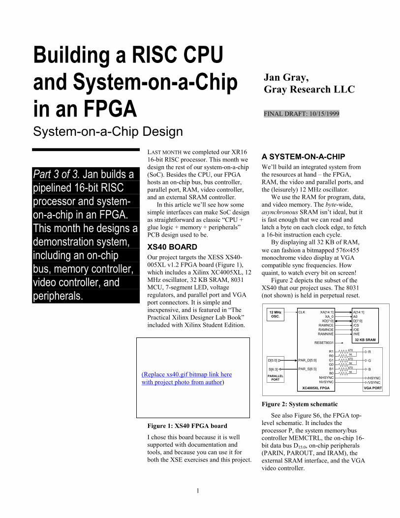
Figure 1: XS40 FPGA board
I chose this board because it is well supported with documentation and tools, and because you can use it for both the XSE exercises and this project.
A SYSTEM-ON-A-CHIP We�ll build an integrated system from the resources at hand � the FPGA, RAM, the video and parallel ports, and the (leisurely) 12 MHz oscillator.
We use the RAM for program, data, and video memory. The byte-wide, asynchronous SRAM isn�t ideal, but it is fast enough that we can read and latch a byte on each clock edge, to fetch a 16-bit instruction each cycle.
By displaying all 32 KB of RAM, we can fashion a bitmapped 576×455 monochrome video display at VGA compatible sync frequencies. How quaint, to watch every bit on screen!
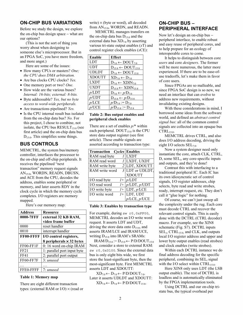
Figure 2 depicts the subset of the XS40 that our project uses. The 8031 (not shown) is held in perpetual reset.
4701K4701K4701K
R
G
B
VGA PORT
/HSYNC/VSYNC
XC4005XL FPGA
XA[14:1]XA_0
XD[7:0]RAMNCERAMNOERAMNWE
RESET8031
R1R0G1G0B1B0
NHSYNCNVSYNC
CLK
PAR_D[5:0]
PAR_S[6:3]
32 KB SRAM
A[14:1]A0D[7:0]/CS/OE/WE
D[5:0]
S[6:3]
PARALLELPORT
12 MHzOSC.
Figure 2: System schematic
See also Figure S6, the FPGA top-level schematic. It includes the processor P, the system memory/bus controller MEMCTRL, the on-chip 16-bit data bus D15:0, on-chip peripherals (PARIN, PAROUT, and IRAM), the external SRAM interface, and the VGA video controller.
(Replace xs40.gif bitmap link here with project photo from author)
2
ON-CHIP BUS VARIATIONS Before we study the design, we explore the on-chip bus design space − what are our options?
(This is not the sort of thing you worry about when designing to someone else�s microprocessor. But in an FPGA SoC, you have more freedom, and more angst.)
Here are some of the issues: • How many CPUs or masters? One;
the CPU does DMA arbitration. • Are bus clocks CPU clocks? Yes. • One memory port or two? One. • How wide are the various buses?
Internal: 16-bits; external: 8-bits. • Byte addressable? Yes, but no byte
access to word-wide peripherals. • Are transactions pipelined? Yes. • Is the CPU internal result bus isolated
from the on-chip data bus? No. For this project, I chose to combine, not isolate, the CPU bus RESULT15:0 (see first article) and the on-chip data bus D15:0. This simplifies some things.
BUS CONTROLS MEMCTRL, the system bus/memory controller, interfaces the processor to the on-chip and off-chip peripherals. It receives the pipelined �next transaction� memory request signals AN15:0, WORDN, READN, DBUSN, and ACE from the CPU, decodes the address, enables some peripheral or memory, and later asserts RDY in the clock cycle in which the memory cycle completes. I/O registers are memory mapped.
Here�s our memory map:
Address Resource 0000-7FFF external 32 KB RAM,
video frame buffer 0000 reset handler 0010 interrupt handler FF00-FFFF I/O control registers,
8 peripherals ×××× 32 bytes FF00-FF1F 0: 16 word on-chip IRAM FF21 1: parallel port input byte FF41 2: parallel port output FF60-FF7F 3: unused � � FFE0-FFFF 7: unused
Table 1: Memory map
There are eight different transaction types: (external RAM or I/O) × (read or
write) × (byte or word), all decoded from AN15:0, WORDN, and READN.
MEMCTRL manages transfers on the on-chip data bus D15:0 and the external data bus XD7:0 by asserting various tri-state output enables (xT) and control register clock enables (xCE):
Enable Effect LDT D7:0 ← DOUT7:0 UDT D15:8 ← DOUT15:8 UDLDT D7:0 ← DOUT15:8 XDOUTT XD7:0 ← D7:0 LXDT D7:0 ← XDIN7:0 UXDT D15:8 ← XDIN15:8 p/LDT D7:0 ← p/D7:0 p/UDT D15:8 ← p/D15:8 p/LCE p/D7:0 := D7:0 p/UCE p/D15:8 := D15:8
Table 2: Bus output enables and peripheral clock enables
There are a set of enables p/* within each peripheral. DOUT15:0 is the CPU store data output register (see first article). These enable signals are asserted according to transaction type:
Transaction Cycles Enables RAM read byte 1 LXDT RAM read word 1 LXDT, UXDT RAM write byte 2 LDT, XDOUTTRAM write word 3 LDT or UDLDT,
XDOUTT I/O read byte 1+ p/LDT I/O read word 1+ p/LDT, p/UDT I/O write byte 1+ LDT, p/LCE I/O write word 1+ LDT, UDT
p/LCE, p/UCE
Table 3: Enables by transaction type
For example, during sw r0,0xFF00, MEMCTRL decodes an I/O write word request. It asserts LDT and UDT, driving the store data onto D15:0, and asserts IRAM/LCE and IRAM/UCE, writing D15:0 into IRAM�s SRAMs:
IRAM/D15:0 := D15:0 ← P/D/DOUT15:0 Next, consider a store to external RAM: sw r0,0x0100. Since the external data bus is only eight bits wide, we first store the least-significant byte, then the most-significant byte. First MEMCTRL asserts LDT and XDOUTT:
XD7:0 ← D7:0 ← P/D/DOUT7:0. Later it asserts UDLDT and XDOUTT:
XD7:0 ← D7:0 ← P/D/DOUT15:8.
ON-CHIP BUS −−−− PERIPHERAL INTERFACE Now let�s design an on-chip bus − peripheral interface, to enable robust and easy reuse of peripheral cores, and to help prepare for an ecology of interoperable cores to come.
It helps to distinguish between core users and core designers. The former will be more numerous, the latter more experienced. If there are to be ease-of-use tradeoffs, let�s make them in favor of core users.
Since FPGAs are so malleable, and since FPGA SoC design is so new, we need an interface that can evolve to address new requirements, without invalidating existing designs.
With these considerations in mind, I borrowed some ideas from the software world, and defined an abstract control signal bus: all of the common control signals are collected into an opaque bus CTRL15:0.
MEMCTRL drives CTRL, and also does I/O address decoding, driving the eight I/O selects SEL7:0.
Now a system designer need only instantiate the core, attach CLK, CTRL, D, some SELi, any core-specific inputs and outputs, and they�re done!
Contrast this with interfacing to a traditional peripheral IC. Each IC has its own idiosyncratic set of control signals, I/O register addresses, chip selects, byte read and write strobes, ready, interrupt request, etc. They don�t call it �glue logic� for nothing.
Of course, we can�t just sweep all the complexity under the rug. Each core must decode CTRL and recover the relevant control signals. This is easily done with the DCTRL (CTRL decoder) macro. For example, see the XIN8 schematic (Fig. S7). DCTRL inputs SELi, CTRL15:0, and CLK, and outputs local I/O register address and upper and lower byte output enables (read strobes) and clock enables (write strobes).
Within each DCTRL instance we do final address decoding for the specific peripheral, combining its SELi signal with the I/O select within CTRL15:0.
Here XIN8 only uses LDT (the LSB output enable). The rest of DCTRL is loadless and is automatically eliminated by the FPGA implementation tools.
Using DCTRL and our on-chip tri-state bus, the typical overhead per
3
peripheral is just one or two CLBs and perhaps a column of TBUFs.
How does control signal abstraction help? So long as we revise MEMCTRL and DCTRL together, we can make arbitrary changes to CTRL15:0 without invalidating any existing designs! And to add new bus features, simply design a new decoder DCTRL_v2, causing no changes to existing DCTRL clients.
EXTERNAL PERIPHERAL INTERFACE? There isn�t one. If it were necessary to attach external peripherals, perhaps to the XD7:0 bus, we might design some on-chip �external peripheral adapter� macros. Just like an on-chip peripheral, each adapter would take CTRL and some SELi, but its job would be to use additional I/O pins to control its peripheral IC�s chip selects and so forth. Of course, as a CTRL15:0 client, it would be able to insert wait states, etc., on behalf of its peripheral.
EXTERNAL RAM The external RAM is a classic 32 KB fast asynchronous SRAM with a 15 ns access time (tAA).
Refer to Figure 2 and the �External Bus and SRAM Interface� block of Figure S6. Table 5 below summarizes the external RAM interface.
FPGA RAM Description XA14:1, XA_0 A14:0 byte address XD7:0 D7:0 data bus RAMNCE /CS chip select RAMNWE /WE write enable RAMNOE /OE output enable
Table 4: FPGA/RAM interface
XA14:1 are 14 IOBs configured as OFDXs (output flip-flops with clock enables). XA14:1 captures the next address AN14:1 at the start of each new memory transaction. XA0 (XA_0) is the least significant bit of the external address. It is a logic output and can change on either CLK edge.
XD7:0 are eight IOBs configured as eight sets of simultaneous OBUFTs (tri-state output buffers), IBUFs (input buffers) and IFDs (input flip-flops).
During a RAM write, XDOUTT is asserted, RAMNOE is deasserted, and the OBUFTs drive D7:0 out onto XD7:0.
During a RAM read, XDOUTT is deasserted, RAMNOE is asserted, and
the RAM drives its output data onto XD7:0. These data are input through the IBUFs and also are latched in the XDIN IFDs (on each falling CLK edge).
Read transactions: To keep the CPU busy with fresh new instructions, we contrive to read both bytes of a 16-bit word in one cycle. In the first half cycle, we set XA0=0, read the MSB, and latch it in XDIN. In the second half cycle, we set XA0=1, read the LSB, and input it through IBUFs. The catenation of these two bytes, XDIN15:0, feeds the CPU�s INSN port, the video controller�s PIX port, and D15:0 via the byte-wide tri-state buffers LXD and UXD.
Write transactions: Writes to asynchronous SRAM requires careful design. Can we safely write one byte per clock cycle? Let�s see. The key constraints are: • address valid before asserting /WE; • data valid before deasserting /WE; • /WE must be deasserted briefly; • no address/data hold time after /WE. We desire a fully synchronous design (so we can slow or stop the clock) and are therefore unwilling to employ any asynchronous delay tricks.
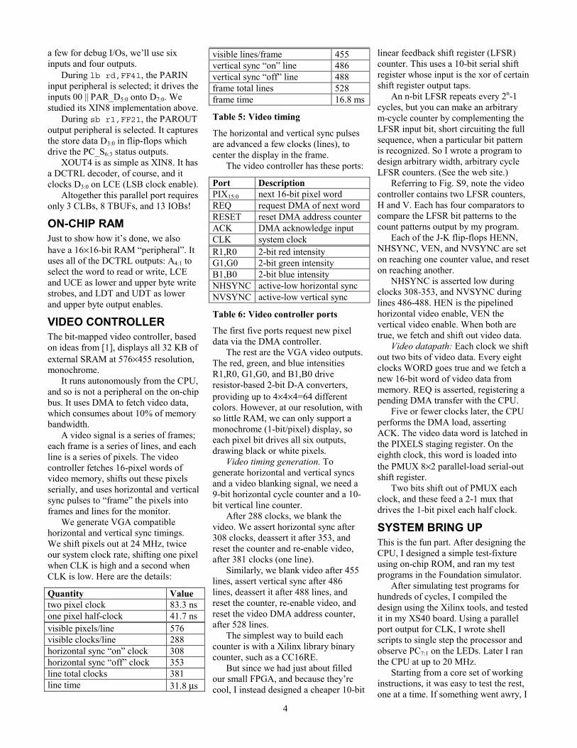
It follows that we need one half clock to settle the write address, one half clock to assert /WE, and one half clock to deassert it. Therefore byte writes take two full cycles, and word writes take three. For example, a word write takes six half cycles W1-W6: • W1: assert XA14:1, data LSB, XA0=1 • W2: assert /WE • W3: deassert /WE, hold XA and data • W4: assert data MSB, XA1=0 • W5: assert /WE • W6: deassert /WE, hold XA and data.
Figure 3 shows three transactions: • read word 1234 from address 0010; • write word ABCD to address 0200; • read word 5678 from address 0012.
READ W1 W2 W3 W4 W5 W6 READCLK
XA[14:1]
XA_0
XD[7:0]
/WE
/OE
0010 0200 0012
12 34 CD AB 56 78
Figure 3: RAM read/write timing
MEMCTRL DESIGN We have discussed its responsibilities: address decoding, on-chip bus control, and external RAM control. Now let�s review its implementation (Fig. S8).
Address decoding: If the next access is a load/store to address FFxx, the access is to memory mapped I/O and SELIO is asserted. Otherwise it�s a RAM access.
Within each peripheral�s DCTRL instance, its SELi (decoded from AN7:5) and CTRLSELIO combine to derive that peripheral�s output and clock enables.
Control: The current state of the memory transaction finite state machine determines which controls are asserted.
The CPU asserts ACE to request the next transaction, and awaits RDY. MEMCTRL decodes the request, and the FSM enters the IO, RAMRD, or RAMWR state. The latter has three sub-states W12, W34, and W56, corresponding to pairs of the W1-W6 half-states described above.
In the IO state, RDY is asserted unless the selected peripheral deasserts CTRL0, the I/O ready line, thereby inserting a wait state.
In the RAMRD state, RDY is asserted immediately, since all RAM reads require only one clock cycle.
In the RAMWR state, RDY is asserted on W34 for byte stores and on W56 for word stores.
The write controller also uses flip-flops W23_45 and W45 which are clocked on CLK falling edges. (That is, W34 is true during W3 and W4, while W45 is true during W4 and W5). From the W* signals we derive glitch-free control signals XA_0, /WE, /OE, etc.
The rest of MEMCTRL is straightforward. Note how E encodes (renames) the various peripheral control signals to CTRL15:0.
I manually technology-mapped some logic using FMAPs. Timing analysis had revealed poor automatic mapping of this logic. This change shaved some nanoseconds off the critical path.
Let�s see about some peripherals.
PARALLEL PORT I/O We provide parallel port I/O to communicate with the host. The XS40 board provides eight parallel port data inputs and five status outputs; reserving
4
a few for debug I/Os, we�ll use six inputs and four outputs.
During lb rd,FF41, the PARIN input peripheral is selected; it drives the inputs 00 || PAR_D5:0 onto D7:0. We studied its XIN8 implementation above.
During sb r1,FF21, the PAROUT output peripheral is selected. It captures the store data D3:0 in flip-flops which drive the PC_S6:3 status outputs.
XOUT4 is as simple as XIN8. It has a DCTRL decoder, of course, and it clocks D3:0 on LCE (LSB clock enable).
Altogether this parallel port requires only 3 CLBs, 8 TBUFs, and 13 IOBs!
ON-CHIP RAM Just to show how it�s done, we also have a 16×16-bit RAM �peripheral�. It uses all of the DCTRL outputs: A4:1 to select the word to read or write, LCE and UCE as lower and upper byte write strobes, and LDT and UDT as lower and upper byte output enables.
VIDEO CONTROLLER The bit-mapped video controller, based on ideas from [1], displays all 32 KB of external SRAM at 576×455 resolution, monochrome.
It runs autonomously from the CPU, and so is not a peripheral on the on-chip bus. It uses DMA to fetch video data, which consumes about 10% of memory bandwidth.
A video signal is a series of frames; each frame is a series of lines, and each line is a series of pixels. The video controller fetches 16-pixel words of video memory, shifts out these pixels serially, and uses horizontal and vertical sync pulses to �frame� the pixels into frames and lines for the monitor.
We generate VGA compatible horizontal and vertical sync timings. We shift pixels out at 24 MHz, twice our system clock rate, shifting one pixel when CLK is high and a second when CLK is low. Here are the details:
Quantity Value two pixel clock 83.3 ns one pixel half-clock 41.7 ns visible pixels/line 576 visible clocks/line 288 horizontal sync �on� clock 308 horizontal sync �off� clock 353 line total clocks 381 line time 31.8 µs
visible lines/frame 455 vertical sync �on� line 486 vertical sync �off� line 488 frame total lines 528 frame time 16.8 ms
Table 5: Video timing
The horizontal and vertical sync pulses are advanced a few clocks (lines), to center the display in the frame.
The video controller has these ports:
Port Description PIX15:0 next 16-bit pixel word REQ request DMA of next word RESET reset DMA address counter ACK DMA acknowledge input CLK system clock R1,R0 2-bit red intensity G1,G0 2-bit green intensity B1,B0 2-bit blue intensity NHSYNC active-low horizontal sync NVSYNC active-low vertical sync
Table 6: Video controller ports
The first five ports request new pixel data via the DMA controller.
The rest are the VGA video outputs. The red, green, and blue intensities R1,R0, G1,G0, and B1,B0 drive resistor-based 2-bit D-A converters, providing up to 4×4×4=64 different colors. However, at our resolution, with so little RAM, we can only support a monochrome (1-bit/pixel) display, so each pixel bit drives all six outputs, drawing black or white pixels.
Video timing generation. To generate horizontal and vertical syncs and a video blanking signal, we need a 9-bit horizontal cycle counter and a 10-bit vertical line counter.
After 288 clocks, we blank the video. We assert horizontal sync after 308 clocks, deassert it after 353, and reset the counter and re-enable video, after 381 clocks (one line).
Similarly, we blank video after 455 lines, assert vertical sync after 486 lines, deassert it after 488 lines, and reset the counter, re-enable video, and reset the video DMA address counter, after 528 lines.
The simplest way to build each counter is with a Xilinx library binary counter, such as a CC16RE.
But since we had just about filled our small FPGA, and because they�re cool, I instead designed a cheaper 10-bit
linear feedback shift register (LFSR) counter. This uses a 10-bit serial shift register whose input is the xor of certain shift register output taps.
An n-bit LFSR repeats every 2n-1 cycles, but you can make an arbitrary m-cycle counter by complementing the LFSR input bit, short circuiting the full sequence, when a particular bit pattern is recognized. So I wrote a program to design arbitrary width, arbitrary cycle LFSR counters. (See the web site.)
Referring to Fig. S9, note the video controller contains two LFSR counters, H and V. Each has four comparators to compare the LFSR bit patterns to the count patterns output by my program.
Each of the J-K flip-flops HENN, NHSYNC, VEN, and NVSYNC are set on reaching one counter value, and reset on reaching another.
NHSYNC is asserted low during clocks 308-353, and NVSYNC during lines 486-488. HEN is the pipelined horizontal video enable, VEN the vertical video enable. When both are true, we fetch and shift out video data.
Video datapath: Each clock we shift out two bits of video data. Every eight clocks WORD goes true and we fetch a new 16-bit word of video data from memory. REQ is asserted, registering a pending DMA transfer with the CPU.
Five or fewer clocks later, the CPU performs the DMA load, asserting ACK. The video data word is latched in the PIXELS staging register. On the eighth clock, this word is loaded into the PMUX 8×2 parallel-load serial-out shift register.
Two bits shift out of PMUX each clock, and these feed a 2-1 mux that drives the 1-bit pixel each half clock.
SYSTEM BRING UP This is the fun part. After designing the CPU, I designed a simple test-fixture using on-chip ROM, and ran my test programs in the Foundation simulator.
After simulating test programs for hundreds of cycles, I compiled the design using the Xilinx tools, and tested it in my XS40 board. Using a parallel port output for CLK, I wrote shell scripts to single step the processor and observe PC7:1 on the LEDs. Later I ran the CPU at up to 20 MHz.
Starting from a core set of working instructions, it was easy to test the rest, one at a time. If something went awry, I
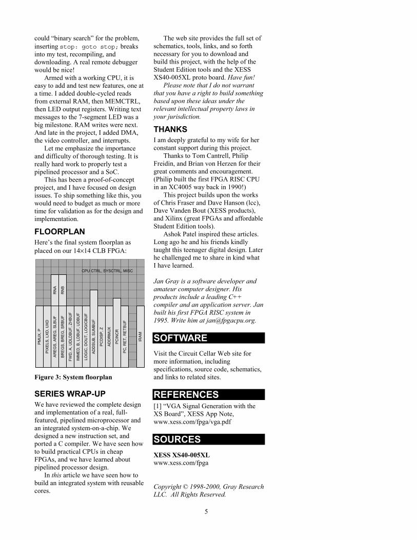
5
could �binary search� for the problem, inserting stop: goto stop; breaks into my test, recompiling, and downloading. A real remote debugger would be nice!
Armed with a working CPU, it is easy to add and test new features, one at a time. I added double-cycled reads from external RAM, then MEMCTRL, then LED output registers. Writing text messages to the 7-segment LED was a big milestone. RAM writes were next. And late in the project, I added DMA, the video controller, and interrupts.
Let me emphasize the importance and difficulty of thorough testing. It is really hard work to properly test a pipelined processor and a SoC.
This has been a proof-of-concept project, and I have focused on design issues. To ship something like this, you would need to budget as much or more time for validation as for the design and implementation.
FLOORPLAN Here�s the final system floorplan as placed on our 14×14 CLB FPGA:
AREG
S, A
REG
, SLB
UF
BREG
S, B
REG
, SR
BUF
FWD
, A, U
DLD
BUF,
ZH
BUF
IMM
ED, B
, LD
BUF,
UD
BUF
LOG
IC, D
OU
T, L
OG
ICBU
F
ADD
SUB,
SU
MBU
F
PCD
ISP,
Z
ADD
RM
UX
PCIN
CR
PC, R
ET, R
ETBU
F
PMU
X, P
PIXE
LS, L
XD, U
XD
IRAM
RN
A
RN
B
CPU CTRL, SYSCTRL, MISC
Figure 3: System floorplan
SERIES WRAP-UP We have reviewed the complete design and implementation of a real, full-featured, pipelined microprocessor and an integrated system-on-a-chip. We designed a new instruction set, and ported a C compiler. We have seen how to build practical CPUs in cheap FPGAs, and we have learned about pipelined processor design.
In this article we have seen how to build an integrated system with reusable cores.
The web site provides the full set of schematics, tools, links, and so forth necessary for you to download and build this project, with the help of the Student Edition tools and the XESS XS40-005XL proto board. Have fun!
Please note that I do not warrant that you have a right to build something based upon these ideas under the relevant intellectual property laws in your jurisdiction.
THANKS I am deeply grateful to my wife for her constant support during this project.
Thanks to Tom Cantrell, Philip Freidin, and Brian von Herzen for their great comments and encouragement. (Philip built the first FPGA RISC CPU in an XC4005 way back in 1990!)
This project builds upon the works of Chris Fraser and Dave Hanson (lcc), Dave Vanden Bout (XESS products), and Xilinx (great FPGAs and affordable Student Edition tools).
Ashok Patel inspired these articles. Long ago he and his friends kindly taught this teenager digital design. Later he challenged me to share in kind what I have learned. Jan Gray is a software developer and amateur computer designer. His products include a leading C++ compiler and an application server. Jan built his first FPGA RISC system in 1995. Write him at [email protected].
SOFTWARE Visit the Circuit Cellar Web site for more information, including specifications, source code, schematics, and links to related sites.
REFERENCES [1] �VGA Signal Generation with the XS Board�, XESS App Note, www.xess.com/fpga/vga.pdf
SOURCES XESS XS40-005XL www.xess.com/fpga
Copyright © 1998-2000, Gray Research LLC. All Rights Reserved.
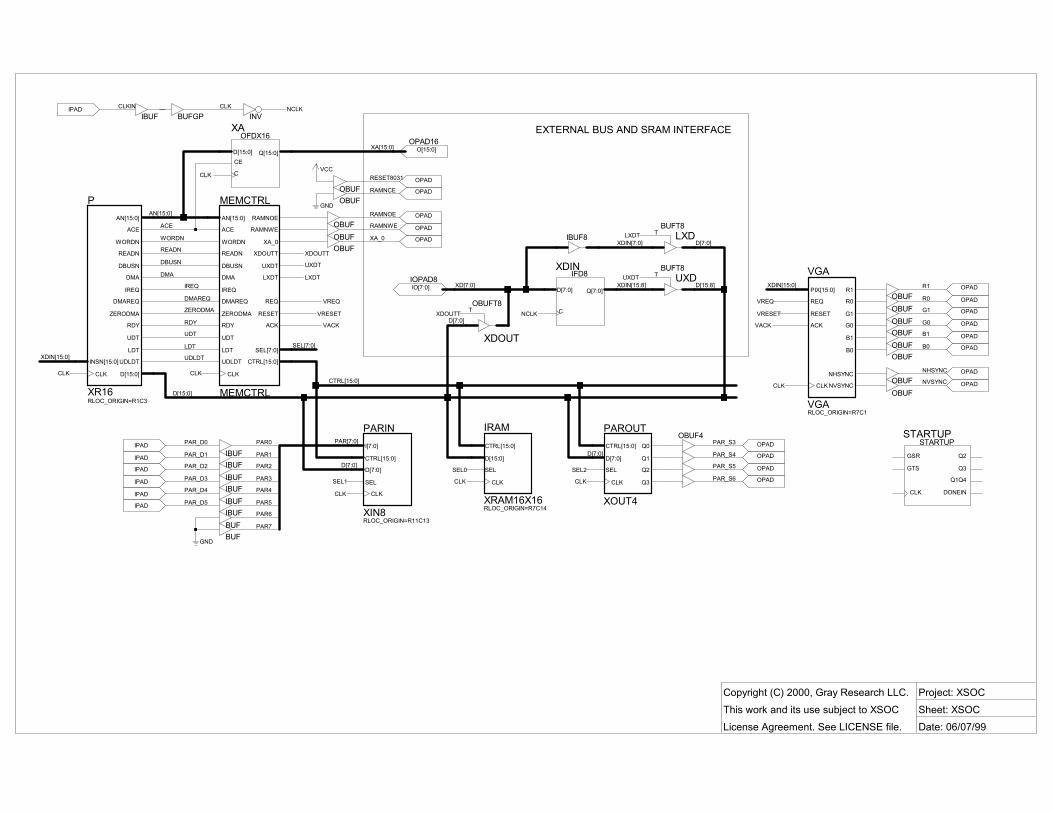
Copyright (C) 2000, Gray Research LLC.This work and its use subject to XSOCLicense Agreement. See LICENSE file.
Project: XSOCSheet: XSOCDate: 06/07/99
EXTERNAL BUS AND SRAM INTERFACE
P
XR16RLOC_ORIGIN=R1C3
CLK
ACE
AN[15:0]
RDY
READN
WORDN
D[15:0]
UDT
LDT
INSN[15:0]
DMA
UDLDT
DBUSN
IREQ
DMAREQ
ZERODMA
OPAD
BUFGP
STARTUPSTARTUP
GSR
GTS
CLK
Q3
Q2
Q1Q4
DONEIN
IBUF
OPAD
INV
OBUF
MEMCTRL
MEMCTRL
AN[15:0]
ACE
WORDN
READN
RDY
UDT
LDT
RAMNOE
RAMNWE
XA_0
XDOUTT
UXDT
LXDT
SEL[7:0]
CLK
CTRL[15:0]UDLDT
REQ
ACK
DMA
DBUSN
IREQ
DMAREQ
ZERODMA RESET
OPAD
IRAM
XRAM16X16RLOC_ORIGIN=R7C14
CTRL[15:0]
D[15:0]
SEL
CLK
OPAD
OBUFOPAD
OBUF OPAD
OBUF
OPAD
XAOFDX16
C
CED[15:0] Q[15:0]
OBUF
OBUF
OPAD
IPADIBUF
XDINIFD8
C
D[7:0] Q[7:0]
IBUF8
UXDBUFT8
T
LXDBUFT8
T
OPAD16O[15:0]
XDOUT
OBUFT8T
OBUFOBUF
BUF
OPAD
PARIN
XIN8RLOC_ORIGIN=R11C13
I[7:0]
CTRL[15:0]
D[7:0]
SEL
CLK
BUF
IPAD
IPAD
IPAD
IPAD
IPAD
IPAD
OPAD
OPAD
IBUFIBUFIBUFIBUFIBUF
OPAD
VGA
VGARLOC_ORIGIN=R7C1
CLK
NHSYNC
NVSYNC
R1
R0
G1
G0
B1
B0
PIX[15:0]
REQ
ACK
RESET
OBUFOBUF
OPAD
OPAD
OBUFOBUF
OPAD
OPAD
OBUF
IOPAD8IO[7:0]
PAROUT
XOUT4
CTRL[15:0]
D[7:0]
SEL
CLK
Q0
Q1
Q2
Q3
OPADOBUF4
AN[15:0]
PAR[7:0]
D[7:0]
XDIN[15:0]
XDIN[15:8]
XDIN[7:0]
XD[7:0]
D[7:0]
D[15:8]
CTRL[15:0]
D[15:0]
D[7:0]
XA[15:0]
SEL[7:0]
XDIN[15:0]
D[7:0]
NCLK
WORDN
CLK
READN
CLK
VCC
RAMNOE
CLK
CLK
RESET8031
RAMNWE
RAMNCE
ACE
GND
LXDT
CLKIN
VRESET
VREQ
VRESET
XA_0
XDOUTT
UXDT
NCLK
LXDT
UXDT
CLK
B0
XDOUTTG0
VREQ
SEL1
B1
CLK
G1
SEL0
DMA
PAR_D0
PAR_D1
PAR_D2
PAR_D3
PAR_D4
PAR_D5
PAR_S5
PAR_S4
PAR7
PAR6
PAR5
PAR4
PAR3
PAR2
PAR1
PAR0
CLK
NHSYNC
NVSYNC
R1
R0
CLK
UDLDT
LDT
UDT
RDY
ZERODMA
DMAREQ
IREQ
VACK VACK
DBUSN
SEL2PAR_S6
PAR_S3
GND
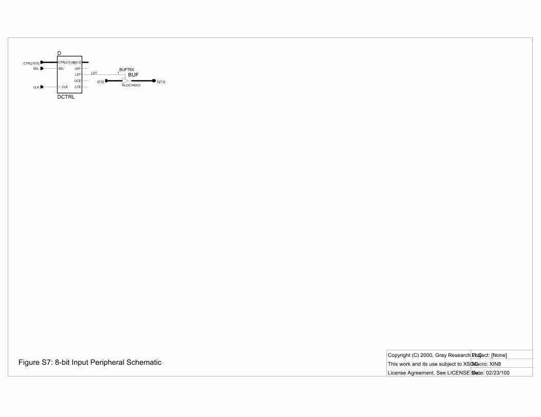
Copyright (C) 2000, Gray Research LLC.This work and its use subject to XSOCLicense Agreement. See LICENSE file.
Project: [None]Macro: XIN8Date: 02/23/100
Figure S7: 8-bit Input Peripheral Schematic
D
DCTRL
CTRL[15:0]
SEL
CLK
UDT
LDT
UCE
LCE
A[4:0]
BUF
RLOC=R0C0
BUFT8XT
D[7:0]I[7:0]
CTRL[15:0]
SEL
CLK
LDT
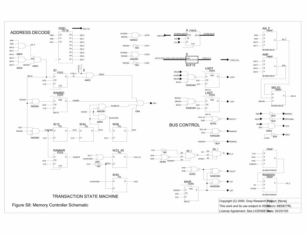
Copyright (C) 2000, Gray Research LLC.This work and its use subject to XSOCLicense Agreement. See LICENSE file.
Project: [None]Macro: MEMCTRLDate: 02/23/100
ADDRESS DECODE
TRANSACTION STATE MACHINE
BUS CONTROL
Figure S8: Memory Controller Schematic
AND2B1 OR4
NOR2
NAND4B1
LXDT
INIT=S
FDPE
D
C
CE
PRE Q
AND3B2
NOR2AND2
NAND2B1
BUF
INV
AND3
DSELD3_8E
A0
A1
A2
D0
D1
D2
D3
D4
D5
D6
D7E
A FD8CE
C
CE
CLR
D[7:0] Q[7:0]
E
BUF16
I[15:0] O[15:0]
INV
M2_1D0
D1O
S0
W45FD
C
D Q
NAND2
NAND2B2
RAMWRFDCE
D
C
CE
CLR
Q
AND2B1
NWR
INIT=S
FDPE
D
C
CE
PRE Q
INV
AND2
M2_1D0
D1O
S0
NAND3B1
UXDT
INIT=S
FDPE
D
C
CE
PRE Q
W12FD
C
D Q
W34FD
C
D Q
NAND2B1
W56FD
C
D Q
OR2
W23_45FD
C
D Q
RAMRD
INIT=S
FDPE
D
C
CE
PRE Q
AND2B1
LLUP
UPIO
FDCED
C
CE
CLR
Q
NOR2
BLKNM=RAMAD0
FMAP
I1
I2
I3
I4
O
RAMAD0
BLKNM=RAMAD0
HMAP
I1
I2
I3O
INV
AND4
AND4
SELIO
BLKNM=SELIO
HMAP
I1
I2
I3O
AN_F
BLKNM=SELIO
FMAP
I1
I2
I3
I4
O
ANF_
BLKNM=SELIO
FMAP
I1
I2
I3
I4
O
BUF
BUF
BUF
AND2
AN[15:0]
UDTN,LDTN,UCEN,LCEN,ACE,SELIO,A[4:0]
SEL[7:0]
CTRL[15:0]
WORD,A[4:0]
CTRL[15:1]
WORDN,AN[4:0]
ACE
NCLK
SELIO
RAMWR
SELIO
RDY
LCEN
XA_0
RAMNOE
W12
READN
RAMWR
W56
W45
W23_45
CLK
AN_F
IORDY
W56
CLK
ACE
IO
READN
ACE
SELIO
AN15
AN13
AN14
SEL0
SEL1
SEL2
SEL3
SEL4
SEL5
SEL6
READNUDTN
ACE
READN LDTN
WORDRAMWR
UDT
A0
WORDN
CLK
READN
READN
WORDN
WORDN
CLK
SEL7
UCEN
DBUSN
XDOUTT
W34WORD
W56
RAMRD
W34
DBUSN
W34
W45
WORD
READNREADN
SELIO
READN
UDLDT
LDT
CLK
W23_45
W34WORD
LXDT
CLK
UXDT
ACE
CLK
ACE
CLK
ACE
CLK CLK
CLK
W12
CLK
W56W34WORD
CTRL0
W23_45RAMNWE
WRRAMNACE
W34BYTE
AN8
AN9
AN10
AN11
AN12
AN5
AN6
AN7
CLK
W45
W56
RAMWR
A0
WORD
XA_0
W45
DBUSN
ANF_
AN_F
AN15
AN13
AN14
AN8
AN9
AN10
AN11
AN12
DBUSN
ANF_
IREQ
ACKDMA
RESET
DMAREQ
ZERODMA
REQ
GND
RDY
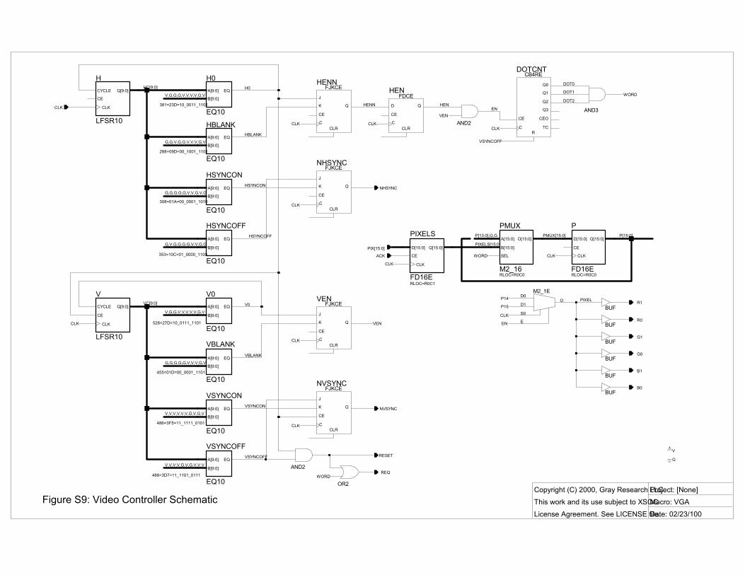
Copyright (C) 2000, Gray Research LLC.This work and its use subject to XSOCLicense Agreement. See LICENSE file.
Project: [None]Macro: VGADate: 02/23/100
381=23D=10_0011_1101
308=01A=00_0001_1010
353=10C=01_0000_1100
528=27D=10_0111_1101
486=3F5=11_1111_0101
488=3D7=11_1101_0111
288=09D=00_1001_1101
455=01D=00_0001_1101
Figure S9: Video Controller Schematic
H
LFSR10
CYCLE
CE
CLK
Q[9:0]
H0
EQ10
A[9:0]
B[9:0]
EQ
HSYNCON
EQ10
A[9:0]
B[9:0]
EQ
HSYNCOFF
EQ10
A[9:0]
B[9:0]
EQ
NHSYNCFJKCE
C
CE
CLR
J
K Q
V
LFSR10
CYCLE
CE
CLK
Q[9:0]
V0
EQ10
A[9:0]
B[9:0]
EQ
VSYNCON
EQ10
A[9:0]
B[9:0]
EQ
VSYNCOFF
EQ10
A[9:0]
B[9:0]
EQ
NVSYNCFJKCE
C
CE
CLR
J
K Q
BUF
BUF
BUF
BUF
BUF
BUF
HENNFJKCE
C
CE
CLR
J
K Q
HBLANK
EQ10
A[9:0]
B[9:0]
EQ
HENFDCE
D
C
CE
CLR
Q
VENFJKCE
C
CE
CLR
J
K Q
AND2
VBLANK
EQ10
A[9:0]
B[9:0]
EQ
PMUX
M2_16RLOC=R0C0
A[15:0]
B[15:0]
SEL
O[15:0]
P
FD16ERLOC=R0C0
D[15:0]
CE
CLK
Q[15:0]
M2_1ED0
D1
E
O
S0
DOTCNTCB4RE
C
CE CEO
Q0
Q1
Q2
Q3
RTC
AND3
PIXELS
FD16ERLOC=R0C1
D[15:0]
CE
CLK
Q[15:0]
AND2
OR2
V,G,G,G,V,V,V,V,G,V
G,G,G,G,G,V,V,G,V,G
G,V,G,G,G,G,V,V,G,G
V,G,G,V,V,V,V,V,G,V
V,V,V,V,V,V,G,V,G,V
V,V,V,V,G,V,G,V,V,V
HC[9:0]
VC[9:0]
G,G,V,G,G,V,V,V,G,V
G,G,G,G,G,V,V,V,G,V
PMUX[15:0] P[15:0]
PIX[15:0]
P[13:0],G,G
PIXELS[15:0]
CLK
NHSYNC
VSYNCON
H0
CLK
HSYNCOFF
HSYNCON
VSYNCOFF
NVSYNC
V0
CLK
CLK
V
G
CLK
R0
G1
G0
B1
B0
VBLANK
HENN
CLK
P15
VEN
R1
HBLANK
CLK
VEN
CLK
PIXELP14
CLK
WORD
HEN
EN
WORD
CLK
VSYNCOFF
RESET
DOT1
DOT2
DOT0
WORDACK
CLK
REQ
EN