building systems for electronic probing of single low
TRANSCRIPT

ACTAUNIVERSITATIS
UPSALIENSISUPPSALA
2011
Digital Comprehensive Summaries of Uppsala Dissertationsfrom the Faculty of Science and Technology 877
Building Systems for ElectronicProbing of Single Low DimensionalNano-objects
Application to Molecular Electronics
SYED HASSAN MUJTABA JAFRI
ISSN 1651-6214ISBN 978-91-554-8212-1urn:nbn:se:uu:diva-160630
and Defect Induced Graphene
Dissertation presented at Uppsala University to be publicly examined in Häggsalen,Ångströmlab, Lägerhyddsvägen 1, UPPSALA. Monday, December 12, 2011 at 10:15 for thedegree of Doctor of Philosophy. The examination will be conducted in English.
AbstractJafri, S. H. M. 2011. Building Systems for Electronic Probing of Single Low DimensionalNano-objects: Application to Molecular Electronics and Defect Induced Graphene. ActaUniversitatis Upsaliensis. Digital Comprehensive Summaries of Uppsala Dissertations fromthe Faculty of Science and Technology 877. 109 pp. Uppsala. ISBN 978-91-554-8212-1.
Nano-objects have unique properties due to their sizes, shapes and structure. When electronicproperties of such nano-objects are used to build devices, the control of interfaces at atomiclevel is required.
In this thesis, systems were built that can not only electrically characterize nano-objects, butalso allow to analyze a large number of individual nano-objects statistically at the example ofgraphene and nanoparticle-molecule-nanoelectrode junctions.
An in-situ electrical characterization system was developed for the analysis of free standinggraphene sheets containing defects created by an acid treatment. The electrical characterizationof several hundred sheets revealed that the resistance in acid treated graphene sheets decreasedby 50 times as compared to pristine graphene and is explained by the presence of di-vacancydefects. However, the mechanism of defect insertion into graphene is different when grapheneis bombarded with a focused ion beam and in this case, the resistance of graphene increasesupon defect insertion. The defect insertion becomes even stronger at liquid N2 temperature.
A molecular electronics platform with excellent junction properties was fabricated wherenanoparticle-molecule chains bridge 15-30nm nanoelectrodes. This approach enabled asystematic evaluation of junctions that were assembled by functionalizing electrode surfaceswith alkanethiols and biphenyldithiol. The variations in the molecular device resistance wereseveral orders of magnitude and explained by variations in attachment geometries of molecules.
The spread of resistance values of different devices was drastically reduced by using a newfunctionalization technique that relies on coating of gold nanoparticles with trityl protectedalkanedithiols, where the trityl group was removed after trapping of nanoparticles in theelectrode gap. This establishment of a reproducible molecular electronics platform enabled theobservation of vibrations of a few molecules by inelastic tunneling spectroscopy. Thus thissystem can be used extensively to characterize molecules as well as build devices based onmolecules and nanoparticles.
Keywords: Graphene, defect induced graphene, molecular electronics, nanoelectrodes,nanoparticles, conductivity, junction, nanomaterial, focused ion beam, surfacefunctionalization, electrical characterization
Syed Hassan Mujtaba Jafri, Uppsala University, Department of Engineering Sciences,Applied Materials Sciences, Box 534, SE-751 21 Uppsala, Sweden.
© Syed Hassan Mujtaba Jafri 2011
ISSN 1651-6214ISBN 978-91-554-8212-1urn:nbn:se:uu:diva-160630 (http://urn.kb.se/resolve?urn=urn:nbn:se:uu:diva-160630)

Dedicated to my family, especially to my late grandmother Zakia Fatima and to my parents Farman Jafri and Prof. Rafia Shereen.


List of Papers
This thesis is based on the following papers, which are referred to in the text by their Roman numerals.
I Conductivity engineering of graphene by defect formation
Jafri S.H.M., Carva K., Widenkvist E., Blom T., Sanyal B., Frans-son J., Eriksson O., Jansson U., Grennberg H., Karis O., Quinlan R.A., Holloway B.C. and Leifer K. Journal of Physics D: Applied Physics, v.43, 045404 (2010)
II An in-situ prepared nano-manipulator for electrical characteri-zation of free standing graphene like sheets inside a focused ion beam/scanning electron microscope Blom T., Jafri S.H.M., Widenkvist E., Jansson U., Grennberg H., Quinlan R.A., Holloway B.C. and Leifer K. Journal of Nanoelectronics and Optoelectronics, v.6, 168-174 (2011)
III In-situ electrical characterization during defect insertion in exfo-liated graphene sheets with a focused gallium ion beam at room and cryogenic temperatures Blom T., Jafri S.H.M., di Cristo V. and Leifer K. In manuscript
IV Fabrication and characterization of high resistance sub 5nm nanogaps made by electrodeposition of gold in 30nm gaps cut by using a focused gallium ion beam Blom T., Jafri S.H.M., Körber N. and Leifer K. In manuscript
V Large variations in shelf-life of gold nanoelectrode gaps and molecular electronic devices stored in air, water and organic solvents Jafri S.H.M., Blom T., Wallner A., Ottosson H. and Leifer K. In manuscript

VI Assessment of a nanoparticle bridge platform for molecular electronics measurements Jafri S.H.M., Blom T., Strømme M., Leifer K., Löfås H., Grigoriev A., Ahuja R. and Welch K. Nanotechnology , v.21, 435204 (2010)
VII Low-temperature synthesis of photoconducting CdTe nano-tetrapods Sugunan A., Jafri S.H.M., Qin J., Blom T., Toprak M.S., Leifer K. and Muhammed M. Journal of Materials Chemistry, v.20, 1208-1214 (2010)0)
VIII Control of junction resistances in molecular electronic devices fabricated by FIB Jafri S.H.M., Blom T., Wallner A., Welch K., Strømme M., Ot-tosson H. and Leifer K. Microelectronic Engineering, v.88 (8), 2629-2631(2011)
IX Formation and NMR spectroscopy of ω-thiol protected α,ω-alkanedithiol-coated gold nanoparticles and their usage in mo-lecular charge transport junctions Wallner A., Jafri S.H.M., Blom T., Gogoll A., Leifer K., Baum-gartner J. and Ottosson H. Langmuir, 27 (14), 9057-9067 (2011)
X Realization of highly reproducible molecular junctions in a na-noparticle-alkanedithiol-nanoelectrode bridge platform Jafri S.H.M., Blom T., Wallner A., Löfås H., Grigoriev A., Ahuja R. , Ottosson H. and Leifer K. In manuscript
XI Vibrational signatures in inelastic tunneling spectroscopy from short molecule-nanoparticle chains trapped in versatile nanoe-lectrodes Leifer K., Jafri S.H.M., Löfås H., Fransson J., Agustsson J., Blom T., Grigoriev A., Ahuja R., Wallner A., Calame M. and Ottosson H. In manuscript
Reprints were made with permissions from the respective publishers.

Author’s contribution to the papers included in this thesis
I. I designed in-situ electrical measurement system, carried out electri-cal measurements and data analysis of the results. I wrote major part of the experimental section in the manuscript.
II. I performed electrical measurements, carried out data analysis, con-tributed to the parts of the manuscript writing.
III. I prepared some of the contacted exfoliated graphene devices, de-signed parts of the in-situ setup, performed parts of experiments, and contributed in data analysis. I contributed to the manuscript writing.
IV. I contributed to the experimental protocol, procedure and SEM anal-ysis, the electrical measurements and in writing of the manuscript.
V. I designed the experimental protocol, carried out parts of SEM anal-ysis, fabricated molecular junctions, contributed in nano-structuring, carried out electrical characterization, data analysis and wrote the major part of manuscript.
VI. I fabricated molecular junctions, contributed in nano-structuring, carried out electrical measurements, data analysis and contributed a major part in writing of the manuscript.
VII. I fabricated the junctions, contributed in nano-structuring and carried out electrical measurement. I did data analysis and wrote part of the manuscript related to physical properties measurement.
VIII. I fabricated the molecular junctions, contributed in nano-structuring, performed electrical measurements, carried out data analysis and wrote major part of the manuscript.
IX. I developed protocol for conductivity measurement, carried out SEM analysis, fabricated molecular devices, contributed in nanostructur-ing, carried out electrical characterization and data analysis. I wrote parts of manuscript related to SEM and electrical characterization.
X. I fabricated the molecular junctions, contributed in nanostructuring, performed measurements, carried out data analysis and wrote the experimental part of the manuscript.
XI. I fabricated the molecular junctions, contributed in nanostructuring, contributed to the measurements, carried out data analysis and con-tributed in writing of the manuscript.
Also Published
Transparent and conducting TiO2: Nb thin films prepared by spray pyrolysis technique Mageto M. J., Maghanga C.M., Mwamburi M., Jafri S.H.M., Leifer K., Niklasson G.A., and Granqvist C.G. In manuscript Nanoparticle bridges for studying electrical properties of organic mole-cules Leifer K., Welch K., Jafri S.H.M. and Blom T. Book Chapter in “Nanoparticles in Biology and Medicine. Methods and Applications” Humana Press, USA (Springer Science + Business Media) Submitted Conduction properties of layer-by-layer self-assembled multilayer na-noparticulate structures Promnimit S., Jafri S.H.M., Sweatman D., and Dutta J. J. Nanoelectron. Optoelectron. v.3, 184-189 (2008) DOI: 10.1166/jno.2008.213 DC analysis of layer by layer devices fabricated by nanotechnology Jafri S.H.M. and Dutta J. Electrical Engineering, 2007. ICEE '07. International Conference on , pp.1-6, 11-12 (2007) DOI: 10.1109/ICEE.2007.4287323 Current-voltage characteristics of layer-by-layer self-assembled colloi-dal thin films Jafri S.H.M., Sharma A. B., Sweatman D. and Dutta J. Applied Physics Letters, v.89, 133123 (2006) DOI: 10.1063/1.2358089 Directed self-assembly of multilayer thin films of zns and gold nanopar-ticles by modified polyelectrolyte deposition technique Jafri S.H.M., Sharma A. B., Thanachayanont C. and Dutta J. MRS 2005 fall meeting, Boston, MA. Rb18.1 (2005) DOI:10.1557/proc-0901-rb18-01

Conference Contributions
Conduction properties of graphene as a function of ion irradiation and acid treatment Blom T., Jafri S.H.M., de Cristo V., Carva K., Possnert G., Sanyal B., Grennberg H., Jansson U., Eriksson O. and Leifer K. Poster presentation at the Imagine nano: Graphene 2011, Spain (2011) Tuning of conduction properties of graphene by defects insertion using chemical and physical means Jafri S.H.M., Blom T., Carva K., Possnert G., Sanyal B., Grennberg H., Jansson U., Eriksson O. and Leifer K. Poster presentation at the Tropical research meetings on Physics: graphene and related two-dimensional materials, United Kingdom (2011) Use of a nanoelectrode nanoparticle bridge platform in molecular elec-tronics Leifer K., Blom T., Jafri S.H.M., Welch K., Strømme M., Löfås H., Grigoriev A. and Ahuja R. Poster presentation at the 5th International Conference on Molecular Elec-tronics, Elcmol’10, France (2010) Control of conductivity in graphene by formation of defects Leifer K., Blom T., Jafri S.H.M., Carva K., Sanyal B., Grennberg H., Jans-son U., Holloway B.C., Quinlan R. and Eriksson O. Poster presentation at the 5th International Conference on Molecular Elec-tronics, Elcmol’10, France (2010) Control of junction resistances in molecular electronic devices fabricat-ed by FIB Jafri S.H.M., Blom T., Welch K., Löfås H., Grigoriev A., Ahuja R., Strømme M.and Leifer K. Poster presentation at the 36th International Conference on Micro and Nano Engineering, MNE2010, Italy (2010) FIB Fabrication and use of high resistance nanogaps for application in molecular electronics Leifer K., Blom T., Jafri S.H.M., Welch K., Strømme M., Löfås H., Grigoriev A. and Ahuja R. Oral presentation at the 17th International Microscopy Congress, IMC17, Brazil (2010)
Dielectrophoretic trapping of gold nanoparticles on SAM-prepared nanogaps: A comparative study of different molecular systems Blom T., Jafri S. H.M., Welch K., Strømme M. and Leifer K. Oral presentation at the International Conference on Molecular Electronics, Emmetten, Switzerland (2010). Molecular electronics on non-perfect electrode surfaces Leifer K., Blom T., Jafri S.H.M., Welch K., Strømme M., Coronel E. and Grigoriev A. Poster presentation at the International Conference on Molecular Electron-ics, Emmetten, Switzerland (2010). In-situ contacting of nanosheets and remote EMCD Rubino S., Jafri S.H.M., Blom T., Carva K., Sanyal B., Fransson J., Eriks-son O., Widenkvist E., Jansson U., Grennberg H., Karis O., Quinlan R. A., Holloway B. C., Lidbaum H., Rusz J., Oppeneer P., Hjörvarsson B., Liebig A., Schattschneider P., Stöger-Pollach M., Hurm C., Zweck J. and Leifer K. Oral presentation at the 2nd International Workshop on Remote Electron Microscopy and In-situ studies, Gothenburg, Sweden (2009). Fabrication and use of high resistance nanogaps for application in mo-lecular electronics Blom T., Jafri S.H.M., Welch K., Strømme M. and Leifer K. Poster presentation at the Micro and Nano Engineering conference (MNE2009), Ghent, Belgium (2009). Electrical characterization of defect induced graphene nanosheets Jafri S.H.M., Carva K., Widenkvist E., Blom T., Sanyal B., Fransson J., Eriksson O., Jansson U., Grennberg H., Karis O. and Leifer K. Oral presentation at Nanotech Europe 2009, Berlin, Germany (2009) Using a nano-contact platform for evaluating molecular electronics re-sponse Jafri S.H.M., Blom T., Welch K., Strømme M. and Leifer K. Poster presentation at Nanotech Europe 2009, Berlin, Germany (2009) Dielectrophoretic trapping of gold nanoparticles on SAM-prepared nanogaps: A comparative study of different molecular systems Blom T., Jafri S.H.M., Welch K., Strømme M., Coronel E., Grigoriev A. and Leifer K. Poster presentation at the European Conference on Molecular Electronics (ECME2009), Copenhagen, Denmark (2009).
Fabrication and characterization high resistance nanogaps used for studies of different molecular electronics systems Blom T., Jafri S.H.M., Welch K., Strømme M. and Leifer, K. Poster presentation at Scandem, Reykjavik, Iceland (2009). The effect of induced vacancy defect on resistivity of graphene Jafri S.H.M., Blom T., Carva K., Widenkvist E., Sanyal B., Fransson J., Eriksson O., Jansson U., Grennberg H., Karis O., Quinlan R. A., Holloway B. C. and Leifer K. Poster presentation at Scandem, Reykjavik, Iceland (2009) Assessment of electrical properties of graphene nanosheets containing defects Blom T., Jafri S.H.M., Carva K., Widenkvist E., Sanyal B., Fransson J., Eriksson O., Jansson U., Grennberg H., Karis O., Quinlan R. A., Holloway B. C. and Leifer K. Oral presentation at the 1st Nordic Workshop on Graphene, Uppsala, Swe-den (2009). In-situ nanomanipulation setup for electrical characterization of grpahene nanosheets inside a FIB-SEM Jafri S.H.M., Blom T., Widenkvist E., Jansson U., Grennberg H., Karis O., Quinlan R. A., Holloway B. C. and Leifer K. Poster presentation at the 1st Nordic Workshop on Graphene, Uppsala, Swe-den (2009). Do-It-Yourself graphene production, transfer and characterization Calvaca F., Jafri S.H.M., Blom T., Akhtar S., Rubino S. and Leifer K. Poster presentation at the 1st Nordic Workshop on Graphene, Uppsala, Swe-den (2009). Control of Conductivity in Graphene by Formation of Defects Jafri S.H.M., Blom T., Carva K., Widenkvist E., Sanyal B., Fransson J., Eriksson O., Jansson U., Grennberg H., Karis O., Quinlan R. A., Holloway B. C. and Leifer K. Oral presentation at the AVS 55th International Symposium & Exhibition, Boston, USA (2008) Self organization of gold nanoparticles and its applications Sugunan A., Promnimit S., Jafri S.H.M.,Dutta J. Oral presentation at the International Conference on Lasers and Nano-materials (ICLAN), Kolkata, India (2006)

Device Characterization of Multilayer Films from Colloids Jafri S.H.M., Sharma A. B.,and Dutta J. Poster presentation at the Eighth International Conference on Nanostruc-tured Materials NANO, Bangalore, India (2006) Characterization of Layer by Layer devices fabricated by nanotechnol-ogy Jafri S.H.M., Promnimit S., Thanachayanont C. and Dutta J. Oral presentation at the New Technologies for Urban Safety of Mega Cities in Asia (USMCA 2006), Phuket, Thailand (2006)
Contents
1 Introduction ......................................................................................... 17 1.1 Materials for next generation electronics ........................................ 18 1.2 Aims and objective of the thesis ..................................................... 21 1.3 Thesis structure and outline ............................................................ 22
2 Physical properties of nano-entities with metallic contacts ................. 25 2.1 Electronic structure and coulomb blockade in nanoparticles .......... 25 2.2 Electron transport through the molecular wires .............................. 27 2.3 Two-dimensional graphene sheets .................................................. 32 2.4 Probing techniques for conduction measurement of nanoparticles and molecules ........................................................................................... 35 2.5 Graphene exfoliation, contact resistance and gating effect ............. 38 2.6 Nano-contacting via dielectrophoretic trapping .............................. 41 Chapter summary ..................................................................................... 42
3 Characterization of nano-entities and techniques for electrical contacts fabrication ..................................................................................................... 44
3.1 Structural Characterization of Nano-entities ................................... 44 3.2 Setup for electrical characterization of nano-entities ...................... 49 3.3 Focused Ion beam Microscopy ....................................................... 50 3.4 Electron beam lithography and Photolithography ........................... 52 3.5 Fabrication of the nanoelectrode platform ...................................... 54 Chapter summary ..................................................................................... 58
4 Conduction properties of graphene and defect induced graphene ....... 59 4.1 Conduction properties of graphene with defects ............................. 59 4.2 Defects in graphene induced by chemical means ............................ 60 4.3 Defects in graphene induced by physical means ............................. 65 Chapter Conclusions ................................................................................ 67
5 Preparation of the nanoelectrode platform for electrical characterization of molecules and nanoparticles........................................... 69
5.1 Sub-5nm nano gaps for direct measurements on molecules ........... 69 5.2 Shelf-life of nanogaps in air, water and organic solvents ............... 71 5.3 Dielectrophoretic trapping of metallic nanoparticles ...................... 72 5.4 Control of junction resistance in between nanoelectrodes and metallic nanoparticles ............................................................................... 74

5.5 Physical properties measurement of semi-conductor nanoparticles by dielectrophoretic trapping .................................................................... 75 Chapter Conclusions ................................................................................ 77
6 Gold nanoparticle-nanoelectrode bridge platform in electrical characterization of molecules down to a single molecule ............................. 78
6.1 Molecular resistance as a function of metal-molecule contact configuration ............................................................................................ 79 6.2 Molecules in bridge platform by self-assembled monolayer formation on nanoelectrodes .................................................................... 80 6.3 Monothiolated molecules in bridge platform by coating of molecules on gold nanoparticles surfaces ................................................ 84 6.4 Dithiolated molecules in bridge platform by coating of -thiol protected molecules on gold nanoparticles surfaces ................................ 86 6.5 Shelf-life of molecular devices in air, water and organic solvents . 92 6.6 Inelastic electron tunneling spectroscopy of 1,8-octanedithiol molecules in nanoparticle-nanoelectrode bridge platform ....................... 92 Chapter Conclusions ................................................................................ 95
7 Concluding remarks ............................................................................. 96 7.1 Outlook ........................................................................................... 97
Summary in Swedish .................................................................................... 99
Acknowledgements ..................................................................................... 102
References ................................................................................................... 104

Abbreviations
AFM Atomic Force Microscopy EBL Electron Beam Lithography ESEM Environmental SEM FEG Field Emission Gun FIB Focused Ion Beam IPA Isopropyl Alcohol or Isopropanol LOM Light Optical Microscopy MCBJ Mechanically Controllable Break-Junction PL Photolithography UV Ultraviolet MIBK Methyl Isobutyl Ketone PMMA Polymethyl Methacrylate SEM Scanning Electron Microscopy STM Scanning Tunneling Microscopy TEM Transmission Electron Microscopy I-V Current-Voltage F-N Fowler-Nordheim IETS Inelastic electron Tunneling spectroscopy HOMO-LUMO Highest occupied molecular orbital-lowest unoccu-
pied molecular orbital OT 1-octanethiol ODT 1,8-octanedithiol BPDT 4,4´-biphenyldithiol HDT 1,6-hexanedithiol DT 1-dodecanethiol AuNP, AuNPs Gold nanoparticle, gold nanoparticles eV Electron-volts R,ρ,σ Resistance, resistivity, conductivity Ohms (SI unit of resistance ) µ, n, p, f Micro 10-6, nano 10-9, pico 10-12, femto 10-15 k, M,G,T Kilo 103,mega 106, giga 109, tera 1012


17
1 Introduction
The discovery of the solid state transistor in 1947 had revolutionized the field of electronics and laid the foundation of the modern electronics era [1]. Today’s electronics is based on networks of billions of transistors fabricated from semiconductor materials such as silicon and germanium [2].
In the last 25 years, global demand for ultrafast cheap and smart electron-ics has increased exponentially. To meet these demands, the integrated cir-cuit (IC) industry has successfully managed to make faster and cheaper de-vices by packing more transistors per unit area by reducing the size of the transistor from 10µm (1971) to 32nm (2010-11) in the industrial scale pro-duction [3]. IC industry has followed G. Moore’s prediction that the number of transistors per IC will double every two years [4]. In the last 20 years, the next generation of logic circuits had twice the transistors per unit area and memories density increased 4 times than the previous generations. However scaling is not a straight forward issue, the size of the transistor has entered a domain where limits imposed by the laws of physics have been reached. The problem is not only in the integrity of devices itself but also in the manufac-turing process. The intrinsic properties of the materials especially silicon are posing a serious challenge to build faster and economical electronic devices [5]. The general issues related to the scaling are thickness of the gate oxide, contact electrodes thickness, intrinsic channel resistance, etc. [6]. In these devices, flow of the electrons carries the signal, which propagates through the fastest available processor in 0.3 ns in the best case limited by transmis-sion characteristics of material used in these ICs. The flow of electrons gen-erate heat and that must be dissipated for safe operation of these devices [7].
Scientists and researchers are trying to discover, fabricate or invent new exotic and exciting nanomaterials that can overcome the challenges posed by silicon based electronics. In the recent past, several new nanomaterials have demonstrated potential to replace silicon technology. Experimental and theo-retical works on nanoparticles [8], carbon nanotubes [9], molecules [10] and graphene [11] have shown potential that can reach the limits imposed by physics. Some of the performances (size, mobility) of such upcoming devic-es containing nanomaterials or device architecture go beyond the perfor-mance of silicon devices though there is still a significant development of devices and device physics needed to fabricate commercial devices from such nanomaterials. Nanomaterials offer new insights into physics and engi-neering because when materials shrink down to the nanometer size, ratio of

18
the surface atoms with respect to the total number of atoms increase drasti-cally. Since the asymmetry around the surface atoms places them in the ex-cited state that the physical properties of entire nano-objects gets affected by the surface states. In addition to that, when electrical contacts are made with nanomaterials to probe their physical properties, the contact itself affects the physical properties of the nano-entities. It is important not only to probe the properties of these nano-entities but also to develop a detailed understanding of these contact junctions. In this thesis, the physical properties especially electrical analysis of the nanomaterials down to the level of single nano-objects is carried out. However contacting of nanomaterial is not a straight forward issue, special in-house contacting techniques have been developed and employed to electrically analyze nanomaterials such as nanoparticles, molecules and graphene (Figure 1). Junction properties of the nanomaterials and their contacts have been discussed in detail. The general introduction of nanoparticles, molecules and graphene is presented in the next section in a view of being a foundation material for potential applications in our daily life.
1.1 Materials for next generation electronics Nanoparticles with sizes less than 50nm are considered by many as building blocks of future electronic devices [8, 12]. The surface to volume ratio leads to increased chemical reactivity due to the changes in the activity of holes and electrons. Nanoparticles can be prepared from both top down and bot-tom up approaches. In the top down techniques such as etching, FIB, EBL etc. the nanoparticles are confined in solid substrates in which diffusion of atoms is not possible [13]. In the bottom up approach nanoparticles can be synthesized by using wet chemical method. Nanoparticles can be stabilized in dispersion either by electrostatic charges as shown in Figure 1a or by mol-ecules or polymer coatings that act as steric hindrance and prevent agglom-eration of nanoparticles (Figure 1b)[14]. When the particle size decreases below the bohr radius i.e. rb= ђ2.є/m*e2, of the first excited state, quantum size effects (like size dependent changes in band gap, ballistic condition) occur due to the confinement of the charge carriers [15]. As a result of quan-tum confinement, the conduction band in the metallic nanoparticles (gold, silver etc.) splits into discrete levels with an energy splitting that depends on the nanoparticle size. In semiconductors, the bandgap in nanoparticles is larger as compared to their bulk counterparts. Nanoparticles are considered as quantum dots and show some analogy to atoms. This leads to energy or-bitals having similar symmetries in quantum dots as compared to atoms. The electrons in a quantum dot are physically trapped within potential barriers. Quantum dots could contain few electrons and the addition or removal of even a single electron would result in observable and exploitable effects.

19
These effects rely on the fact that a considerable energy is required to put a single electron on a charged nanoparticle. This effect is called coulomb blockade and can lead to devices being switched on and off at blistering speeds and with very little power. The optical absorption peak in metallic nanoparticles that is due to surface plasmons demonstrate blue shift with decrease in size of the nanoparticles [16].
Figure 1.a) Ionic stabilized nanoparticles in dispersion, where charges around the colloidal particles stabilize by repelling each other. b) Steric hindrance stabilizes the nanoparticles in dispersion, where coating (molecules, polymer) prevent indi-vidual colloidal particles to from agglomeration. c) A schematic representation of an organic molecule (SH (CH2)8SH, 1,8-octanedithiol) having sulfur attached to both end of alkane chain. d) Graphene, a 2D sheet, where carbon atoms are ar-ranged in hexagonal structure having sp2 bonding with neighboring carbon atoms. A ripple effect in graphene makes 2D structure stable in normal conditions.
Molecules as compared to nanoparticles are considered as one dimensional wires (Figure 1c). The original idea of utilizing molecules in electronics was proposed by Aviram and Ratner in 1973 [17]. Typically molecular electron-ics is based on the organic molecules having alkane chains and/or cyclohex-ane rings with lengths of 1-2nm [18]. It is possible to create ultra-dense elec-tronics [19] using molecules due to their nanometric sizes. In order to get to that stage certain hurdles that need to be overcome are to get complete con-
a) b)
c) d)c)
20
trol on the synthesis of molecules and very large scale integration of the molecular systems. The major advantage of molecules is that they can be tailored with almost unlimited variations in the electrical properties. Recent-ly, gating effect in molecules has been demonstrated providing a pathway to build molecule based transistors [20]. One of the great issues to achieve large integration of molecules in a device is connecting a single or few mol-ecules to an electrical circuit that provides reliable and reproducible charac-teristics of the system. A poor covalent bond exists between metallic elec-trodes and molecules, it can generate Schottky-like barrier due to chemical potential that leads to accumulation of charges at zero bias, which may mod-ify the molecule electron density. Thus it was proposed to consider mole-cules with its electrodes as a single system [21]. Another advantage of mole-cules is their arrangement on metallic surfaces by self-assembled monolayer formation (SAM) [22], which allows large scale fabrication of molecular devices. In molecular electronics, electron transfer in the molecules has been studied in liquid and gas phases [23] whereas, electron transport has been studied using scanning tunneling microscopy (STM) [24, 25], nanopores [26], nanoelectrodes prepared by electrodeposition and nanolithography [27, 28] and mechanically controlled break junctions [29-31].
A single layer of carbon atoms arranged in hexagonal structure is known as graphene as shown in Figure 1d [32]. To understand physical properties of graphite made of graphene layers, graphene has been studied theoretically, but it was considered for many decades that 2D crystalline structure cannot exist in nature because classical thermodynamics predicted it to be unstable [33, 34]. However, single layer of graphene was separated on silicon dioxide surface in 2004 [35]. These 2D crystals are of high quality and continuous in which electron can travel without scattering for long distances [36], the mean free path is estimated on a length scale of several micrometers which is limited by edge of graphene and electrical contacts [37]. Graphene flakes with a diameter of several tens of micrometers can be prepared by mechani-cal exfoliation using a scotch tape and later transferring onto 300nm thick thermally grown silicon dioxide (SiO2) on silicon substrate [35]. However large area sheets of graphene can be prepared by using a chemical vapor deposition (CVD) process on metal surfaces such as Ni and Cu[38]. Gra-phene can be prepared by wet chemistry either by intercalation of graphite with ions and separating layers through sonication [39] or by converting graphite into graphite oxide and later reducing it to graphene [40]. Graphene is a zero bandgap material, where conduction and valence band just meets at Fermi level. Graphene exhibits ambipolar electric field effect having carrier concentration in order of 1013 cm−2[35]. Carrier mobility in graphene can be as high as 200,000 cm2 V-1 s-1 depending upon the quality of substrate [41]. Graphene has demonstrated high opacity for a single layer by absorbing 2.3% of white light [42] Thermal conductivity of graphene at room tempera-ture ranges between 4.84 to 5.30× 10³ W/mK [43]. Graphene is considered
21
as the strongest material with breaking strengths of 42 Nm–1 [44]. All of these properties make graphene an ideal candidate for applications not only in electronic devices but also in photonics, ceramics etc.
1.2 Aims and objective of the thesis Low dimensional nano-objects provide basis for devices with excellent and extraordinary properties, but electronic probing of low-dimensional nano-objects often requires an out of the box solution. Every nano-object varies in size, shape and structure, and it is not possible to develop a single or direct method to electrically characterize them irrespective of their morphologies. Electronic probing of nano-objects requires at least two metallic contacts for applying bias voltage and electron conduction. Even a small deviation in morphology of two similar nano-objects can influence their properties con-siderably. The interpretation of such influences is a major hindrance in la-boratory and commercial applications of graphene, nanoparticle and mole-cules. The general aim of this thesis is to build electrical characterization systems that can electronically probe the nano-objects according to their shape, size and structure with full control on nano-contacting as well as the contact junction between them. The general objective of this thesis is to elec-trically characterize the nano-objects in large numbers to understand their electrical properties and electronic structure under different conditions and environments. It is important to control the junction between nano-objects and contacts so that properties of junction do not overshadow those of the material and hence reproducibility could be achieved.
Graphene has shown potential but to use it in electronic applications, its conduction properties must be modified either by chemical or physical means. In first part of this thesis, defects are created in graphene sheets by physical and chemical treatments. An in situ electrical characterization sys-tem should be designed based on the shape and size of graphene sheets as well as experimental parameters. The system should be able to carry out systematic assessment on changes in conduction properties related to defect formation in graphene lattices.
The establishment of a chemical and electrical contact between nanoelec-trodes and nanoparticles is a most critical step in connecting nano-objects and can be, in principle established by molecules. The subsequent electrical analysis of this interface is an essential step to understand this connection or junctions between nano-objects where the electrical signal is then dominated by molecules. Nanogaps with sizes in range of 20-30nm in between gold electrodes have been demonstrated [45], but the size of molecules makes it difficult to directly contact them to fixed electrical leads. The size of mole-cules is at least 20 times smaller than the size of the nanogaps, thus it is re-quired to bridge the gap by the metallic nanoparticles. It is extremely im-

22
portant to control the junction resistance between nanoparticle and nanoelec-trode for molecular characterization otherwise molecular response will be diminished in the contact resistance. The introduction of molecules in be-tween nanoparticle and nanoelectrode is a challenging task. An electrical characterization system needs to demonstrate the metallic nanoparticle-nanoelectrode junction properties. The molecules can be introduced in this bridge platform by the coating of either nanoparticles or nanoelectrodes. The variation in the attachment geometry of molecules to the fixed contacts leaves question marks on repeatability and reproducibility. The stable metal-molecule junctions should be achieved in the nanoparticle-nanoelectrode bridge platform with reproducible electrical and electronic properties. Thus it is required to develop a stable system that can be used to characterize mol-ecules and nanoparticles. As nanoelectrodes can be bridged by the metallic nanoparticles, it can also provide a testbed for the electronic probing of sem-iconductor nanoparticles.
1.3 Thesis structure and outline Although it will take few years to build a commercial device from nanopar-ticles, molecules or graphene, this thesis provides an insight into foundation material for future electronic devices. In this thesis, modification in the con-duction properties of graphene by defect insertion using physical and chemi-cal means is discussed. For electronic probing of nanoparticles and mole-cules, a system based on nanoparticle-nanoelectrode bridge platform is de-veloped that shows an ohmic contact between metallic nanoparticles and nanocontacts. By trapping of semiconductor nanoparticles in between metal-lic nanoelectrodes, its photoconductivity is observed. A stable and solid state platform i.e. nanoelectrode-nanoparticle bridge platform is established for characterization of molecules that forms the basis for molecular electronic devices.
In Chapter 1, a brief introduction has been provided on the basics of modern electronics along with needs and requirement for new material which can ultimately replace silicon based devices. A brief introduction on nanoparticles, molecules and graphene has also been covered in section 1.1. Chapter 2 of the thesis deals with theoretical background on the properties of studied nano-objects. In the first three sections of this chapter (2.1-2.3), electronic structure and electrical response of nanoparticles, molecules and graphene under applied voltage bias are discussed. A brief review on nano-contacting and characterization of nano-objects is presented in section 2.4. Graphene exfoliation, electrical characterization and effect of current anneal-ing are reviewed in section 2.5. In order to achieve electrical contact with nanoparticles and molecules, dielectrophoretic trapping has been carried out. The dielectrophoretic trapping process is also discussed in section 2.6.

23
Chapter 3 provides description and discussion of structural characterization techniques (section 3.1) used in this thesis. Section 3.2 describes the instru-mentation used for electrical characterization of devices. A brief introduction to focused ion beam, electron beam lithography and photolithography is given in section 3.3 and 3.4 respectively. Brief fabrication process of the nanoelectrode platform is mentioned in section 3.3. Chapter 4 deals with defect induced graphene sheets. In section 4.1, theoretical result on the mod-ification of conduction properties with the defects insertion in graphene lat-tices is presented. Change in conduction properties by introduction of defects in graphene nanosheets by chemical means is presented in the section 4.2. In contrast, defects are introduced in exfoliated graphene sheets by physical means using FIB at room and cryogenic temperatures. The change in con-duction due to gallium ions irradiation and the effect of defects creation at liquid nitrogen temperature are discussed in section 4.3. Chapter 5 deals with building a testbed for molecular electronics. Sections 5.1 and 5.2 de-scribe shrinking of the nanogaps in between nanoelectrodes by electrodepo-sition and shelf-life of these nanoelectrodes. Metallic contact between gold nanoparticles (AuNPs) and gold nanoelectrodes is achieved (section 5.3) during dielectrophoretic trapping and trapping of semiconductor nanoparti-cles is presented along with its photoconductive properties (Section 5.5). Chapter 6 deals with introduction of molecules in between AuNPs-nanoelectrodes bridge platform (Section 6.1). 1-octanethiol (OT) and 4,4´-biphenyldithiol (BPDT) are introduced by formation of self-assembled mon-olayer and molecules are characterized (Section 6.2). Electrical characteriza-tion of 1-dodecanethiol (DT) is discussed when AuNPs are coated with mol-ecules along with nanoelectrodes (Section 6.3). Formation of chemisorbed junctions at the both end of molecules in between AuNP and nanoelectrode platform is presented and conduction properties of 1,8-octanedithiol (ODT) and 1,6-hexanedithiol (HDT) is discussed (section 6.4). Shelf life of AuNP-molecule-nanoelectrode platforms is also discussed when stored in ambient conditions, water and organic solvents (section 6.5). In section 6.6, results from inelastic electron tunneling spectroscopy of ODT in between AuNP-nanoelectrode bridge platform is presented. Conclusions and outlooks are presented in chapter 7 along with summary in Swedish and acknowledge-ments in the end.
In paper I, theoretical and experimental studies have been carried out to observe the effect of vacancy defects on graphene sheets, where it has been demonstrated that introduction of the defects decreases the resistivity of gra-phene sheet by 50 times in magnitude. Paper II describes an in-situ tech-nique that can be used to electrically characterize the nano-objects inside FIB/SEM. This technique is based on sharpening of the manipulator tip down to 50nm and manipulating it to make electrical contacts with the nano-objects. Paper III deals with defects creation by 30kV Ga+ ions in exfoliated graphene sheets at room and cryogenic temperatures. In-situ conductivity

24
changes have been measured in graphene sheet when defects are created inside FIB/SEM. Results from Raman spectroscopy and AFM of irradiated graphene sheet has been also presented. Paper IV is also based on gold elec-trodeposition on the FIB cut nanogaps to fabricate a smaller gap size for direct electrical characterization of the molecules. In paper V, shelf life of nanoelectrodes setup and molecular devices in ambient conditions, water and organic solvents is presented. Paper VI deals with creation of AuNP-nanoelectrode bridge platform. OT and BPDT have been introduced by self-assembled monolayer formation on nanoelectrodes to electrically character-ize these molecules. In Paper VII, CdTe based tetrapods are synthesized and dielectrophoretic trapping of these semiconductor nanoparticles have been carried out in between nanoelectrodes to observe photoconductivity in the system. Paper VIII describes different metal-molecule junction that has been formed either by coating of molecules on nanoelectrodes or AuNPs or both. ODT, BPDT and DT molecules are tested and measured in this paper. In paper IX, to create stable chemisorbed junctions -trityl protected 1,8-octanedithiol (PODT) coated AuNPs are synthesized. After trapping, trityl protective groups (deprotection chemistry) are removed to form stable chem-isorbed metal-molecule junctions at the both end of molecules in between two adjacent gold surfaces. Electrical characterization of ODT and HDT using deprotection chemistry is presented in paper X, where it can be ob-served that these devices demonstrate highly reproducible electrical proper-ties and resistances. Theoretical modeling is also carried out to understand the difference in conductivity of these devices before and after the removal of trityl protective groups. In paper XI, inelastic electron tunneling spec-troscopy of ODT molecules in nanoelectrode-nanoparticle bridge platform is discussed in detail. Theoretical calculations has been carried out to identify different molecular vibration peaks in the measured spectra, which lead to the conclusion that this system can be used to for building molecular devices with few molecules.
25
2 Physical properties of nano-entities with metallic contacts
The complete literature background and review on nanoparticles, molecules and graphene sheets is not possible due to the vastness of these topics, but the physical properties of the nanoparticles, molecules and graphene that are probed electrically in this thesis are discussed in detail. The preparation of metal-molecule junction in between 15-30 nm nanogaps requires trapping of the nanoparticles to bridge the gap, thus the electronic structure of confined atoms are described in 2.1. As the physical properties of the molecules are strongly affected by the influence of metallic contacts, a general physics related to molecular wire is discussed in 2.2. In this thesis, the conduction properties of graphene are modified by the defects. In section 2.3 conduction properties of graphene are presented. Measurement techniques that have been employed in literature to measure the conduction properties of nano-objects are given in section 2.4. Graphene production by mechanical exfolia-tion and its electrical characterization are presented in section 2.5. Dielectro-phoretic trapping of the AuNP in between nanoelectrodes is the major tech-nique that has been deployed to characterize 1-2nm molecules in between nanoelectrodes in this thesis. A general introduction to the dielectrophoretic trapping is presented in section 2.6.
2.1 Electronic structure and coulomb blockade in nanoparticles
Two major phenomena are observable in the physical and chemical proper-ties of the nanoparticles that gradually change from solid state to molecular behavior with decreasing particle size. First of all the electronic structure of metal and semiconductor nanoparticles gradually evolves from orbitals like energy levels to the delocalized band structure with increasing particle size. Secondly, the number of surface atoms can be similar to or higher than those located in the crystalline lattice core, in which the surface properties start playing a vital role. The surface atoms remain highly unsaturated and their electronic contribution to the behavior of the nanoparticle is different from that of the inner atoms. These effects may be even more marked when the surface atoms are legated [46]. This leads to the different mechanical and

26
electronic transport properties, which account for the catalytic properties of the nanocrystalline particles [47]. Nanoparticles that show this quantization size effect are sometimes called Q-particles or quantum dots.
In a metal, the quasi-continuous density of states in the valence and the conduction bands splits into discrete electronic levels, the spacing between these levels and the band gap increasing with decreasing particle size[48, 49] as shown in Figure 2a and 2b and its properties can be influenced by the electrical contacts (Figure 2c). Metallic nanoparticles consisting of 50 to 500 atoms with a diameter less than 3nm start to lose their metallic behaviour at room temperature and tend to become semiconductors [50]. In a semicon-ductors, the already existing band gap increases when the particle size is decreased and the orbital like energy levels gradually convert into discrete electronic levels [51]. If the particle size is less than the De Broglie wave-length of the electrons, the charge carriers may be treated quantum mechani-cally as "particles in a box", where the size of the box is given by the dimen-sions of the crystallites as shown in Figure 2d [52].
Figure 2. a) Band structure of semiconductor material, b) band structure of a semi-conductor nanoparticles, c) a schematic representation of trapped nanoparticle coated with a barrier in between metallic electrodes, d) particle in box when parti-cle size is less than de Broglie wavelength.
When size of nanoparticles is comparable to the electron mean free path, their electronic and chemical properties change as compared to bulk proper-ties. A quantum confinement of electrons is observable in the semiconductor nanoparticles [53] and in the small metallic nanoparticles [54]. Another phe-nomenon is plasmons on nanoparticle surfaces which are generated by the coherent oscillation of the free electrons[16].
The quantum confinement of the electrons gives rise to the discrete ener-gy levels, in which discrete energy levels are given as E=ћ2π2n2/2mL2 where L is length of channel n=1,2,3 is discrete levels and m is effective mass of the charge carrier as shown in Figure 2c.
In order to add a single charge to the nanoparticle energy is required. The resistance of barrier increases with applied voltage which is known as cou-lomb blockade. The activation energy of the nanoparticles is given as EC=
NPBULK
Ev
Ec
EgEf
ContactsMetallic NP
n1, E1
n2, E2
n3, E3
Ea) b) c)
d)

27
e2/2C(r), where C(r) is size dependent capacitance of nanoparticle that is given as C(r)=4πєєor and r is radius of nanoparticle [55].
Coulomb blockade is observable in the current-voltage (I-V) characteris-tics when KbT<Ec in metallic and semiconductor nanoparticles [56]. Figure 3 demonstrates the coulomb blockade in I-V characteristics of 5nm AuNP capped with molecules trapped in between the gold electrodes. It can be seen that until the threshold voltage is reached there is no conduction of electrons and after the threshold the current increases nonlinearly with the applied voltage, however due to the large size of nanoparticles it is not possible to observe discrete energy levels. In the nanoparticle-nanoelectrode bridge platform AuNPs are used to bridge the gap. In electrical measurements car-ried at 4K on molecules in AuNP-nanoelectrode bridge platform in this the-sis, coulomb blockade effect was observed (Chapter 6).
Figure 3. Coulomb blockage as observed in current –voltage (I-V) characteristics of molecule coated AuNPs trapped in between the nanoelectrodes measured at 4K.
2.2 Electron transport through the molecular wires Molecules can be tailored into different shapes and geometry that can have unique electronics properties. In organic molecules, atoms are bound through sigma (σ) and pi (π) bonding. The bonding between atoms along determines the conduction properties of a molecule [57]. Interesting molecules usually consist of a push-pull system i.e. donor, accepter and a bridge part [58]. Molecules are considered as a wire made of atoms where electrodes are re-quired to bias the molecules and transfer electron across the molecular wire.
Voltage(bias) (V)
Cur
rent
(A)
Coulomb blockade
28
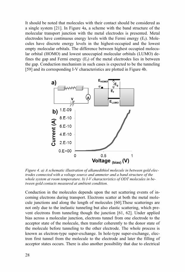
It should be noted that molecules with their contact should be considered as a single system [21]. In Figure 4a, a scheme with the band structure of the molecular transport junction with the metal electrodes is presented. Metal electrodes have continuous energy levels with the Fermi energy (Ef). Mole-cules have discrete energy levels in the highest-occupied and the lowest empty molecular orbitals. The difference between highest occupied molecu-lar orbital (HOMO) and lowest unoccupied molecular orbitals (LUMO) de-fines the gap and Fermi energy (Ef) of the metal electrodes lies in between the gap. Conduction mechanism in such cases is expected to be the tunneling [59] and its corresponding I-V characteristics are plotted in Figure 4b.
Figure 4. a) A schematic illustration of alkanedithiol molecule in between gold elec-trodes connected with a voltage source and ammeter and a band structure of the whole system at room temperature. b) I-V characteristics of ODT molecules in be-tween gold contacts measured at ambient condition.
Conduction in the molecules depends upon the net scattering events of in-coming electrons during transport. Electrons scatter at both the metal mole-cule junctions and along the length of molecules [60].These scatterings are not only due to the inelastic tunneling but also elastic scattering, which pre-vent electrons from tunneling though the junction [61, 62]. Under applied bias across a molecular junction, electrons tunnel from one electrode to the acceptor state of the molecule, then transfer coherently to the donor state of the molecule before tunneling to the other electrode. The whole process is known as electron-type super-exchange. In hole-type super-exchange, elec-tron first tunnel from the molecule to the electrode and later the filling of acceptor states occurs. There is also another possibility that due to electrical
a)
b)
Voltage (bias) (V)
Cur
rent
(A)
e- Eg
EHOMO
Ef
HOMO
ELUMO

29
or thermal excitation electrons can jump into the acceptor state from the donor state. Conduction mechanism in few molecules falls into two different categories i.e. temperature dependent thermionic or hopping conduction and temperature independent direct or Fowler-Nordheim tunneling. Fowler-Nordheim plots are used to interpret data in the physics of field emission. In molecular electronics these plots can be used to determine the nearest mo-lecular level in two terminal devices [63, 64], and this is known as Transition Voltage Spectroscopy (TVS). In Figure 5, the I-V characteristics of a mole-cule is re-plotted as ln(I2/V) vs. 1/V with the corresponding tunneling model described by Simmons model [60].
Figure 5. Transition voltage spectroscopy of alkanedithiol in between AuNP- nanoe-lectrode bridge platform, the I-V characteristics in the Figure4b are repotted in Fowler-Nordheim plot. The electronic structure of molecules with metallic contacts I) at the lower bias voltages (Vb< Ф/e), II) at the bias voltage Vb= Ф/e and III) at the higher bias voltages Vb> Ф/e.
In Simmons model the barrier height is described as the rectangular barrier as shown in Figure 5, in which the barrier height (Ф) is described by the Fermi energy level (Ef) and the HOMO level (EHOMO), whereas the width of the barrier is given by the length of molecule. The current (I) is directly pro-portional to the bias voltage (Vb< Ф/e) and resistance is positive (Figure 5 I), because the effective barrier height decrease with increasing applied bias voltage. At Vb= Ф/e, barrier becomes triangular and appear as minima (Vm) in the plot (Figure 5 II). When Vb> Ф/e, part of the barrier is available for conduction and the slope becomes negative, then the proportionality between
LN [I
/V2 ]
(A/V
2 )
1/V (V-1)
I)
II)
e-
Vb
Eg
EHOMO
Ef
III)
e-
Vb
Eg
EHOMO
Ef
e-
Vb
Eg
EHOMO
Ef

30
current and voltage changes from linear to quadratic (Figure 5 III). Simmons model in the Fowler-Nordheim plot reveals that Vm is directly proportional to the barrier height, independent of the molecular length. This indicates the transition to the Fowler-Nordheim regime from direct tunneling. The meas-urements on the alkanedithiol molecules with gold contacts confirm the the-oretical interpretation from Simmons model [64]. Another model is present-ed as the resonant molecular model where voltage drops at the contacts only [65]. Both models, the Simmons model and resonant molecular model clear-ly verify that the transition voltage spectroscopy allows distinguishing mo-lecular junction from the vacuum junctions because tunnel junction without molecules will be dependent on the length of barrier.
As discussed earlier, with the applied bias electrons from one electrode tunnel to the other electrode without losing energy, the process is known as elastic tunneling as shown in Figure 6a. However if a local state is available then during tunneling electrons can lose energy and give energy to the local state (Figure 6b) and that opens a new conduction channel. This tunneling process is known as inelastic tunneling [66]. In case of electron transport through molecules, the electrons lose their energy only when there is a vibra-tional mode (ω) available and the applied voltage is large enough for elec-trons to have energy eV>ћω [67].
Figure 6. Schematic illustrations of a) elastic tunneling b) inelastic tunneling, If electron tunnels across the barrier without losing energy, the process is known as elastic tunneling in molecules and direct tunneling in solid state physics. When an electron lose energy during tunneling and transfer energy to state present in a gap, such tunneling is known as inelastic tunneling in molecules and indirect tunneling in solid state physics.
Inelastic tunneling of electrons in molecules with small applied voltage indi-cates the presence of molecules and that can be used to identify the molecu-lar species in a junction [68, 69]. Such a technique is known as inelastic electron tunneling spectroscopy (IETS) [70]. As for molecular adsorption on surface, vibrational states of molecules are usually studied with the optical spectroscopy such as infrared (IR)[71], Raman [72], high-resolution electron energy-loss Spectroscopy (HREELS) and UV photoelectron Spectroscopy
e-
Vb
EgEHOMO
Efe-
EHOMO
Ef
ћωa) b)
Vb

31
(UVPS) [73]. Whereas optical spectroscopy techniques need large volume of molecules, inelastic electron tunneling spectroscopy is sensitive down to the individual and single molecule.
Opening of another tunneling channel due to the inelastic tunneling gen-erate a small kink in the I-V curves, which appears as a small step in differ-ential conductance plot and as a peak in second derivate of the current volt-age characteristics as shown in Figure 7 [67]. The electrons that tunnel across a junction are very few and induce a very small change in the current as oscillator period is relatively large, compared to the traversal time.
Figure 7. a) A simple kink in I-V characteristics is due to availability of new chan-nels b) differential conductance plot of where step edges indicate the change in resistance in conduction pathway c) d2I/dV2 vs V indicated the availability of new channels and channel type.
One possibility is to measure IETS signal in the numerical second (2nd) deri-vate of I-V curve but a small noise can introduce a large uncertainty. In order to reduce the noise it is recommended to take 100s of measurement which will in turn average out the noise in system [74]. Normally, a small sinusoi-dal signal with amplitude between 10-30mV and frequency between 10-100Hz is superimposed on a ramping DC bias and 2nd derivative is measured directly using a phase sensitive lock in detection technique[75], which can be expressed as Taylor’s expansion of current with respect to applied bias.
According to this equation, the first and second harmonics measured sig-nal gives the scaled value of first and second derivate of current [70]. There are no specific selection rules as compared to the optical spectroscopy [76, 77] as peaks in second (2nd) derivate do not arise from the dipole interaction but from the vibration modification of the electronic levels [78]. An IETS spectrum is characterized by peak positions, widths and intensities. The peak position can be predicted with known voltage drop across the junction [76]. The peak intensity is dependent on the electron molecule coupling which is difficult to estimate but it can provide information about nature of the mole-cule binding on the surface [78]. The boarding of peaks depends upon the intrinsic line width and as well as on two extrinsic width broadening effect.
0.E+00
5.E-09
1.E-08
2.E-08
0 0.04 0.080.E+00
1.E-08
2.E-08
3.E-08
0 0.04 0.080.E+00
1.E-07
2.E-07
3.E-07
4.E-07
0 0.04 0.08
a) b) c)
Vbias (V) Vbias (V) Vbias (V)
I(A) dI/dV(A/V) d2I/dV2(A/V2)

32
The thermal broadening occurs due to breath of the Fermi level [66] and the predicted value is 5.4kT/e [79]. The molecular vibrational peaks can only be observed at cryogenic temperature due to thermal broadening. The modula-tion broadening occurs due to the dynamic detection technique [67]. The measured experimental 2nd derivative (4I2/V
2) is convolution of exact 2nd derivative (d2I/dV2) and an instrumental function. The half width of this experimental function is 1.7Vrms. The modulation amplitude must be adjust-ed to give required resolution and signal to noise ratio. For better resolution low modulation amplitude is required, whereas the better signal to noise ratio is obtained at higher modulation amplitudes.
2.3 Two-dimensional graphene sheets Graphene, made of carbon atoms in hexagonal structure (Figure 8a, Figure 8b shows graphene in reciprocal space), is a zero band gap material as men-tioned in the Chapter 1 and is considered as a semimetal with a linear disper-sion (Dirac electron) [33]. Band structure of graphene calculated from the tight binding model is shown in Figure 8c. The hopping energy in graphene between different sub lattices is around 2.8eV and in same sub lattices is around 10 times lower [80]. From band diagram it can be observed that at Dirac points (Figure 8b, as Dirac equation becomes valid at this point in reciprocal space) the conduction and valance band just touch each other [81]. The absence of the bandgap deduce that even at a very small bias voltage applied across a graphene sheet, the electrons will have enough energy to move from the valence band to the conduction band and currents starts flow-ing.
Figure 8. a) Graphene honeycomb lattices with carbon carbon distance a=1.42Å, which is further subdivided in two sublattices A and B. Lattice unit vector are de-fined as a1=a/2(3,√3) and a2=a/2(3,-√3), b) corresponding Brillouin zone and the Dirac cones are located at K=(2π/3a, 2π/3√3a) and K’=(2π/3a, -2π/3√3a). c) band structure of graphene lattice demonstrating electron dispersion in Brillouin zone Right: zoom of energy band close to Dirac point. (Figure 8 adopted from the Ref.[81], and reproduced with the permission of APS)
Electronic properties of graphene are reflected from its structure where two adjacent atoms link by σ bond (bond length 1.42Å) having sp2 hybridization.
A Ba1
a2
k
k’
b1
b1
ky
kxM
a) b) c)

33
The p orbital perpendicular to the planar structure forms the π bond. This π band is half filled according to the Pauli-exclusion principal [34]. The half-filled π band strongly affects the electronic properties of a graphene sheet e.g. electron mobility of the suspended graphene is at least 10 times higher than graphene on substrate [82]. Electrons in the graphene can propagate over several micrometer without scattering [35].
Conduction in graphene follows Dirac equation and charge carrier acts as two dimensional Dirac fermions [36] except for the speed of these fermions, which is 300 times less than speed of light [83]. The integer quantum Hall effect [84, 85] in graphene can be measured and interestingly this effect can be observed at room temperature [86]. Furthermore other interesting proper-ties related to graphene are Klein paradox [87] and Zitterbewegung [88]. The Klein paradox arises when Dirac fermions are insensitive to the external electrostatic potentials and tunnel across a barrier with a probability of 1.
Figure 9. a) Change in resistivity (2D resistivity has unit in k) with an applied electrical field controlled by gate voltage (Vg). Insets shows band structure of gra-phene at applied gate voltages where Fermi energy level changes with an electrical Field (Figure 9a is adopted from the Ref.[32],. Gate voltage induces carrier concen-tration n=αVg for field effect devices with 300nm SiO2 as a dielectric. b) Quantum Hall effect, where massless Dirac fermions shows staircase in σxy at half integer of 4e2/h (Figure 9b is adopted from the Ref.[36]). (Reprinted with the permission of nature publishing group)
As mentioned in Chapter 1, graphene flake on thermally grown 300nm SiO2 on silicon substrate can be identified in the optical microscope. A natural advantage of graphene on SiO2 substrate is that electrical contacts can be prepared and electrical field can be applied by establishing an electrical con-tact to the silicon substrate underneath SiO2. The application of an electrical field on the graphene through the silicon substrate will be called backside gate or gate in the following. This gate allows to measure field effect con-duction properties of graphene [35]. As shown in Figure 9a, graphene exhib-its change in conductivity with backside gate due to quenching of available
a) b)

34
conduction states as charge carriers can be tuned in electron and hole with applied gate voltage as observed in Hall coefficient measurements [32]. At a certain applied gate voltage graphene exhibits a minimum conductivity due to the fact that conduction becomes ballistic at the Dirac point. Another theo-retical prediction indicates that the presence of random charge impurities produce a minimum conductivity at low induced carrier density without rul-ing out any other universal mechanism. The charge impurities create a spa-tially inhomogeneous screened coulomb potential. The system breaks up into puddles of electron and holes that effects local chemical potential and induce the residual charge density [89]. The conductivity increases linearly on both sides of the minimum conductivity with the increasing and decreasing elec-trical field but there are no zero conductance regions in graphene.
As shown in Figure 9b, a monolayer graphene exhibits staircase hall con-ductivity (σxy) with change in charge carrier from electrons to hole [36]. Each step is changed by ½ (half integer) with respect to quantum hall re-sistance, the staircase follows σxy=±4e2/h(N+½) where N is Landau level and 4 is due to double spin degeneracy and double valley. This quantization of electronic spectrum is described by EN=±νF(2eћBN)½ in a magnetic field B and quantized level exists at zero E which is occupied by electrons and holes [85, 90, 91].
Graphene electronic structure can be modified by extrinsic and intrinsic disorder. The modification of the potentials in the graphene crystals such as induced by impurities or vacancies affect sensitively electronic properties of graphene. This can be observed in spectroscopic and transport properties. Graphene has demonstrated strong scattering feature associated with transport properties due to the charged impurities in the SiO2 substrate and removal of charge impurities the room temperature electron mobility can be improved to 4x104 cm2v-1s-1 on SiO2 which is limited by remote interfacial phonon scattering [41]. Another source of intrinsic defects in graphene are structural defects such as Stone Wales defects [92]. Such defects cause the minimum conductivity over a large range of the carrier density in graphene [93]. Extrinsic defects, such as doping strongly influence the conductivity of graphene sheets. Adsorption and desorption of only a single molecule affects the local carrier density and can be observed as a step like change in conduc-tivity [94]. The attachment of oxygen and water molecules leads to signifi-cant hole doping in graphene sheets [95]. In addition, oxygen can be trapped in between graphene and the substrate interface also leading to hole doping [96].
Irradiation of graphene with an electron beam at 30kV affects the transport properties of graphene by n-type doping of graphene sheets, this is due to the underneath substrate interactions [97]. A 10kV electron beam inducing inter bond disorder but the electron energies are too low for lattice damage [98]. In contrast, ion beam irradiation at 30kV results in sputtering of graphene but sputtering rates are less than expected [99]. Graphene struc-

35
ture changes from nanocrystalline to amorphous and the electron transport regime changes from diffusion transport to carrier hopping [100]. It is pre-dicted that graphene with a grazing incidences (60O) ion beam (few tens of eV to 10MeV) increases the sputtering rate but reduces amorphized areas in the lattices [101]. In addition to that point defects (vacancies) results in the local magnetic moments. Such local magnetic moments affect electron con-duction through Kondo effect [102].
2.4 Probing techniques for conduction measurement of nanoparticles and molecules
One of the main challenges in electrical characterization is to contact the nano-objects to the measurement instruments. Metallic leads need to be pre-pared by the conventional and the unconventional advance structuring tech-niques that can contact a nano-sized object from the opposite sides ends. Nanoparticles and molecules are in the order of several nanometers. There are several techniques to carry out such measurements that have been pro-posed and demonstrated in the past, a brief review of these techniques is presented here.
Figure 10. Schematic illustrations of different measurement techniques to analyze nanoparticles a) monolayer deposition of nanoparticles b) conductive AFM or STM (STS) on dispersed nanoparticles on a conductive surface d) trapped nanoparticles in between nanogaps fabricated by advance fabrication techniques.
A simple and quick approach is to measure a collective response by deposit-ing a thin film of the nanoparticles and molecules on a conducting substrate while other electrical contact is prepared on top of film as shown in Figure 10a. Nanoparticulate films can be prepared by using either spin coating or sedimentation or dip coating or Langmuir-Blodgett method [55, 103, 104]. The electrical characterization of a single nanoparticle usually starts with a dispersion of nanoparticle on the conductive substrate and by making contact with the individual nanoparticles by using either conductive atomic force microscopy (Figure 10b) [105] or by scanning tunneling spectroscopy [106]. The major route of nano-contacting that has been demonstrated by several group is dielectrophoretic trapping of nanoparticles in between nanogaps (Figure 10c) [107-109]. Nanogaps can be prepared by electron beam lithog-raphy [110, 111], electrodeposition [111], electromigration [112] and by
Conductive substrate
AVbMetallic contacts Nanoparticles
Conductive substrate
Nanoparticles
AVV
Insulating substrate
AMetallic tip Metallic
contacts Nanoparticles
a) b) c)
36
cutting metallic lines with focused ion beam [108]. An excellent review about preparation of nanogaps can be found in Ref. [113].
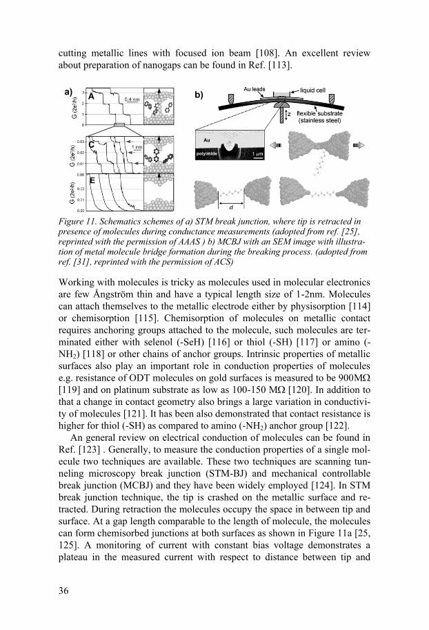
Figure 11. Schematics schemes of a) STM break junction, where tip is retracted in presence of molecules during conductance measurements (adopted from ref. [25], reprinted with the permission of AAAS ) b) MCBJ with an SEM image with illustra-tion of metal molecule bridge formation during the breaking process. (adopted from ref. [31], reprinted with the permission of ACS)
Working with molecules is tricky as molecules used in molecular electronics are few Ångström thin and have a typical length size of 1-2nm. Molecules can attach themselves to the metallic electrode either by physisorption [114] or chemisorption [115]. Chemisorption of molecules on metallic contact requires anchoring groups attached to the molecule, such molecules are ter-minated either with selenol (-SeH) [116] or thiol (-SH) [117] or amino (-NH2) [118] or other chains of anchor groups. Intrinsic properties of metallic surfaces also play an important role in conduction properties of molecules e.g. resistance of ODT molecules on gold surfaces is measured to be 900M [119] and on platinum substrate as low as 100-150 M[120]. In addition to that a change in contact geometry also brings a large variation in conductivi-ty of molecules [121]. It has been also demonstrated that contact resistance is higher for thiol (-SH) as compared to amino (-NH2) anchor group [122].
An general review on electrical conduction of molecules can be found in Ref. [123] . Generally, to measure the conduction properties of a single mol-ecule two techniques are available. These two techniques are scanning tun-neling microscopy break junction (STM-BJ) and mechanical controllable break junction (MCBJ) and they have been widely employed [124]. In STM break junction technique, the tip is crashed on the metallic surface and re-tracted. During retraction the molecules occupy the space in between tip and surface. At a gap length comparable to the length of molecule, the molecules can form chemisorbed junctions at both surfaces as shown in Figure 11a [25, 125]. A monitoring of current with constant bias voltage demonstrates a plateau in the measured current with respect to distance between tip and
a) b)

37
surface. The first plateau with high conduction is an indication of metal-metal contact until breakage of metallic contact displaying conductance quantization in steps of 2e2/h [126], the next plateau indicates the molecular resistance as molecules slips into a gap thereby forming a metal molecule junction as shown in Figure 11a (left panel). Further increase in distance leads to the measured current value of zero due to breakage of metal-molecule junction at the tip [127]. In MCBJ, a thin wire is fabricated by electron beam lithography on a SiO2 surface and a drop of solution is placed on the thin wire, which is then elongated and finally broke by bending the substrate using piezo motors as shown in Figure 11b [29, 31]. The conduct-ance measurement technique is same as in the STM break junction tech-nique.
Figure 12. Schematic illustrations of molecular characterization by formation of self-assembled monolayers a|) with liquid metal top contact b) nanopores with top and bottom contact c) a simplified cross bar structure.
The other techniques that are employed to measure collective response of few molecules have been carried out by formation of SAM layer of mole-cules. One of the initial measurements on SAM layer has been carried out by using liquid metal (mercury) as a top electrode as shown in Figure 12a [128]. However the fabrication of a top electrode may result in short-circuit by filamentary growth of metals [129]. A more sophisticated method is to create a nanopore in an insulating layer on top of a conducting substrate, then a small number of molecules forms defect free SAM layer in nanopores. The top electrode is fabricated to measure molecular conductance as shown in Figure 12b [130]. Another variation in fabrication of the metal-molecule junction is prepared by cross bar structure as shown in Figure 12c [131], where SAM assembled monolayer is formed on either one or two metallic wire and gentle contact between two wires constitute a metal molecule junc-tion [132].
Alternatively, in order to characterize the molecules are to coat metallic nanoparticles with them, a general review on synthesis of nanoparticles in given in Ref. [14]. Using Langmuir-Blodgett technique, a large area mono-layer film of nanoparticles can be prepared and the molecules in such nano-particle- molecule films can be electrically contacted using electron beam lithography [133]. The top-down approach is consists of preparing nanogap
Metallic Plate
Mercury Droplet
Metallic Plate
Top Contacta) b) c)

38
in between gold nanoelectrodes prepared by electron beam lithography, fo-cused ion beam cutting, electromigration and evaporation with the gold elec-trodes [113]. The nanogap can be bridged by the metallic nanoparticles. A direct approach is to trap nanoparticles in between nanogap either by AC electrical field [107] or by external magnetic field [134].
Figure 13. I-V characteristics of 30nm AuNP coated with OT trapped in between nanoelectrodes. (Inset, SEM image of device)
Scanning electron microscope (SEM) image of a trapped AuNP coated with OT with the corresponding I-V characteristics is shown in Figure 13. The I-V measurement shows molecular response of few OT in the AuNP-nanoelectrode bridge platform. Molecules can also be introduced in such junction by coating of the nanoelectrodes with molecules by forming self assembled monolayer of thiol terminated molecules. Later the nanogap can be bridged either by the deposition of AuNPs from colloidal dispersion on the electrodes [135] or by the evaporation of gold at slow evaporation rate at the gap region [136]. A major hurdle in this technique is the estimation of the number of molecules taking part in transport, as it is possible to have double or triple or multiple junctions. This gives rise to an uncertainty in the absolute value of resistance per molecule in addition to the charging effect at the metal-molecule junction.
2.5 Graphene exfoliation, contact resistance and gating effect
Graphene is as thin as 3Å but exfoliated flakes can be as large as 10-100µm. Monoatomic layer and few layer of graphene sheets can be prepare by me-chanical exfoliation of graphite crystals and transferred to a SiO2 substrate for contacting and characterization [35]. Highly Oriented Pyrolytic Graphite (HOPG) or Kish graphite can be used to prepared graphene sheets. A com-mon scotch tape is placed on the top of the HOPG and upon the removal of
-1.0E-10
0.0E+00
1.0E-10
2.0E-10
-3 -2 -1 0 1 2 3
200nm
Cur
rent
(A)
Voltage bias (V)

39
the tape cleavage of the surface layers from HOPG occurs. To obtain gra-phene, flakes attached to the tape are cleaved again and again by folding the scotch tape until a uniform thin layer is obtained (Figure 14a).
Figure 14. a) Camera pictures of cleaved HOPG on scotch tape and thinning of HOPG by repeated folding of scotch tape and b) transfer of flakes from tape to the 300nm thick SiO2 thermally grown on the silicon substrate, c) light optical image of the graphene flake where the stronger contrast indicates multilayer graphene flake (1) and the lighter contrast indicates a monolayer or bilayer graphene (2).
Figure 15. a) Light optical microscope image of the graphene flake with large con-tact for electrical characterization using manual probe station b) I-V characteristics of contacted graphene sheet demonstrating effect of current annealing, after every I-V measurement sheet is treat with an increasing current step of 100µA for 0.6 sec.
Later, a portion of tape is placed on top of the thermally grown 300nm thick silicon dioxide (SiO2) on the silicon substrate. Flakes are transferred by ap-plying a gentle pressure on the tape, which is followed by rubbing (Figure 14b). To locate a graphene flake, the substrate is scanned in an optical mi-croscope at low magnification (5X or 10X). The light optical microscopy is discussed in detail in section 3.1.1. In case of a suitable candidate higher magnification image is recorded. The lighter contrast indicates the presence of a thinner graphene flake and a darker contrast corresponds to thicker graphite flake (Figure 14c). The verification of single layer graphene flake is done by atomic force microscopy (AFM) and Raman spectroscopy. The details and implementations of these two techniques are given in section 3.1.3 and 3.1.4 respectively.
It is relatively easy to electrically contact graphene flakes lying flat on an insulating substrate by using conventional electron beam lithographic (EBL)
a) b) c)SiO2
2
1
Heating Step 100µA heating
for 0.6s
20
10
0
-10
-200 0.5 1-0.5-1
Voltage bias (V)
Cur
rent
(μA
)
Gold contacts
Graphene flake
a) b)

40
technique and photolithography (PL) as shown in Figure 15a (details about EBL and PL are given in 3.4). However, scattering effect in graphene de-creases the mobility of electrons and influences electronic properties of gra-phene. This occurs due to the underneath substrate, the graphene structural defects, ripples and charge impurities from adsorbents (discussed in section 2.3). In order to reduce the scattering source, current or heat annealing is usually carried out. In the heat annealing process, graphene on Si/SiO2 sub-strate is heated at 300oC in inert gas atmosphere [137]. In the current anneal-ing process, the sample is treated with large biasing current as shown in Fig-ure 15b [138]. Unclean graphene demonstrates a non-linear I-V response, but after current annealing the I-V response transits towards linearity. Con-tinued heating yields an ohmic behavior of graphene as shown in Figure 15b.
Figure 16. Change in conductivity (2D conductivity has unit in S) with an applied electrical field controlled by gate voltage, Ug . Inset, schematic illustration of gated measurement setup G is indication on of the graphene flake in the schematic.
The back gated response of graphene sheets can be measured by applying voltages of up to several tens of volts to the silicon substrate underneath SiO2. The contact with the silicon substrate can be made by either drilling a hole using the FIB or etching of SiO2. In Figure 16, the gated response of a graphene sheet is plotted. The conductivity of graphene decreases with the applied gate voltage and reaches a minimum conductivity level. The conduc-tivity of graphene sheet again increases with change in the applied gate volt-age. The minimum of the conductivity in the gated curves is influenced by the substrate and can appear on either side of the applied gate voltage. The slope represents electrons and holes mobility. The asymmetry in the slope usually comes from the unbalance contribution from hole and electrons. The
0 50 100-50-100
1.8
1.4
1
0.6
Gate Voltage, Ug (V)
Con
duct
ivity
2D(m
S)
SiliconSiO2
Au GVb
AUg

41
unbalance contribution indicates the presence of more holes than electronics or vice versa. The field effect carrier mobility (µFET) is given by [139]
where toxide is the thickness of SiO2 (300nm), є is relative dielectric constant of SiO2 (3.9), L is the length of flake and W is the width of flake. The esti-mated field effect carrier mobility of the exfoliated graphene flakes used in this thesis is ~1600 cm2V-1s-1. Considering field effect carrier mobility as real carrier mobility, the number of 2D charge carrier density in the graphene sheets is estimated to be ~2.6x1012 cm-2, which is comparable to reported values [139, 140].
2.6 Nano-contacting via dielectrophoretic trapping Dielectrophoretic trapping of nanoparticles is widely employed in this thesis (Chapter 4 and 5) to fabricate AuNP-nanoelectrode bridge platform. Dielec-trophoretic trapping occurs due to polarization of uncharged particle [141]. As shown in Figure 17a, a particle is suspended in a non-uniform electrical field. Under the influence of applied electrical field (E) particle becomes polarized and the polarization P (units C/m-2) is given as [142]
where є0 is permittivity of free space and χe is the susceptibility. The result-ant electrical field induces an electrical displacement (D) given by
The force will develop due to interaction of the induced charges on each side with the electrical field and the electrical fields lines [143] as shown in Fig-ure 17a. The particles will move towards the highest electrical field region if the medium around the particle is less polarizable than the particles because dipoles align with the electrical field. In case of the negative dielectrophro-sis, particles are less polarizable than medium around it and dipole aligns itself against electrical field and particle moves in opposite direction to the high electrical field [144]. The dielectrophoretic force is dependent on the induced dipole and independent of direction of the electrical field. Since the alignment field is irrelevant the force can also be generated by AC fields [145]. AC electrical fields (E) eliminate possibility of electrophoretic forces. Dielectrophoretic force (F) on a spherical body with a radius (r) is given by

42
where єm is the complex relative permittivity of medium, whereas, K(w) is defined as complex permittivity factor in terms of єm and єp
Polarized particles in a rotating electrical field experience induced dipole
across the particle and rotate in synchrony with the field. Similarly, non-spherical particles under electrical field rotate such that dipole along the longest non-dispersed axis aligns with the field. Rod shape particle will align its longest axis with electrical field at low frequency but at higher frequency the particle will rotate 900 and align perpendicular to the field. In addition to that non-charged particles are also influenced by electrical field via electro-orientation and electro-rotation effects as shown in Figure 17a [145]. It has been demonstrated that in between the nanoelectrodes positive dielectropho-retic forces exist that increases towards the nanogap in between electrodes as shown in Figure 17b and simulation shows highest field strength occurs on electrodes edges [146].
Figure 17. a) Schematic illustration of polarized nanoparticle suspended within a point plain electrode system. When the particle is polarized, force exerted due to interaction of charges with electrical field (adopted from ref. [145]) b) Simulation results of the electric field distribution using FERMILAB, electric filed contour in the nanoelectrode setup (adopted from ref. [146] and reproduced with the permis-sion of IOP).
Chapter summary The discrete energy levels in nanoparticles have made them interesting can-didates for use in basic electronic devices. Nanoparticles demonstrate Cou-
-
+
-- ---
+++++
Net force
107a) b)

43
lomb blockade and can act as quantum dots where a measureable effect can be observed when single electrons are added to the particles. The nanoparti-cles can be electrically characterized either by fabricating films of nanoparti-cles with large electrical contact pads or by using conductive tips in AFM or STM or by using a nanoelectrode setup.
In contrast molecules used for electrical measurements are often so short that they must always be considered as a single system along with their elec-trical contacts. Electrical characterization of a single molecule is usually carried out by STM break junction or MCBJ techniques. At the macro scales, films of the molecules can be characterized by using either liquid metal contacts or nanopores with top-bottom contacts or cross-bar junctions. Conduction through molecules at low bias occurs due to non-resonant tun-neling of electrons. During tunneling, the electrons may lose energy to excite a molecular vibration, which can be considered as a molecular signature and can be identified in IETS. The AuNP-nanoelectrode bridge platform pro-vides a stable setup to characterize and build molecular devices that consist of a few molecules. The molecules can be introduced on the surfaces of ei-ther AuNPs or nanoelectrodes. The AuNP-nanoelectrode bridge platform can be prepared first by fabrication of nanoelectrodes and later the gap in be-tween nanoelectrode is filled with AuNPs. Dielectrophoretic trapping is widely used to trap nanoparticles in between nanoelectrodes.
Graphene is a 2 dimensional material and has demonstrated an extra ordi-nary potential due to its unique band structure. Monolayers of graphene can be exfoliated and contacted with metallic electrodes on SiO2 substrate. The charge carriers in graphene act as 2-D Dirac fermions, which travel at speed 300 times less than light. At Dirac point, the conduction band and valence band just touch each other, thus upon application of small bias voltage con-duction starts in graphene. Graphene has demonstrated quantum hall effect, Klein paradox and Zitterbewegung. Electronic properties of graphene are strongly influenced by adatoms, absorbents and defects, which makes gra-phene an ideal candidate for future electronic devices.

44
3 Characterization of nano-entities and techniques for electrical contacts fabrication
In this thesis, structural characterization of nano-objects has been carried out intensively at every step of the fabrication and the electrical measurement to verify integrity and stability of the measurement systems. In section 3.1, structural characterization techniques that were extensively used in this the-sis are described. Details of the electrical characterization equipment are given in section 3.2. Focused ion beam (FIB) has been used in fabrication of nano-contacts and milling of nanogaps. A brief introduction on FIB is given along with electron beam lithography (EBL) and photolithography (PL) in section 3.3 and 3.4. In section 3.5, fabrication of the nanoelectrodes setup that has been used for characterization of nanoparticles and molecules is described in detail.
3.1 Structural Characterization of Nano-entities The visualization of nano-object is one of the main challenges in the recent times and requires special sample preparation or equipment. Every nano-object poses a different technical challenge for visualization. There are cer-tain standardized techniques to structurally characterize nano-entities, but these techniques require special preparation of nano-objects e.g. molecules can be visualized using STM but STM on devices containing molecules is still a technological challenge. Light optical microscope, electron micro-scopes, atomic force microscope and Raman spectroscope have been used to structurally characterize the nano-objects in this thesis.
3.1.1 Light optical microscopy Light optical microscope is the nondestructive technique to study sub-micron objects. Optical microscopes have been available since 1600AD and now it has resolution down to 200nm with white light source. The resolution is directly dependent on the wavelength of the light source. Advanced optics have made it possible to resolve sub-100nm structures with visible light [147]. Light optical microscopy is a quickest way to observe results of pho-

45
tolithographic and electron beam lithographic patterns and structures as shown in Figure 18a.
The optical microscopy has become a useful tool in identifying the mono-layer of carbon atoms (graphene) on a SiO2 substrate after discovery of gra-phene sheets as shown in Figure 18b [147]. It is possible to differentiate between a thin and thick graphene flakes using this technique. In this thesis, an optical microscope - Olympus AX70 has been used extensively to identi-fy graphene flakes on SiO2 substrates. In addition to that it is also employed to check EBL results after each process step during fabrication of nanoelec-trodes and graphene contacts.
Figure 18. a) Light optical microscope image electron-beam lithography developed pattern b) light optical microscope image of graphene flakes on top 300nm thick SiO2 on Si substrate. Thin and thick flakes can be differentiated in the reflection image.
3.1.2 Electron microscopy Electron microscopy is based on two techniques a) scanning electron mi-croscopy, b) transmission electron microscopy. As mentioned the earlier, resolution is directly dependent on wavelength of the incident beam which is dependent on accelerating voltages of the electron microscopes. The wave-length of electrons is 12.3pm in SEM at an accelerating voltage of 10kV. In the transmission electron microscopes (TEM) that usually operate at acceler-ating voltage of 200-300kV, the wavelength of electron is 2.5pm for acceler-ating voltage of 200kV. It means that it is possible to observe material down to atomic level using electron microscopes. Typical resolution in the SEM is in order of 2-3nm and in the TEM is in order of 0.5-2Å. The primary elec-tron beam interacts with sample and generates various signals as shown in Figure 19a.
The SEM usually operates up to 30kV accelerating voltage. Two main signals that are generated from electron-sample interactions are utilized for imaging i.e. a) the electrons which are generated near surface (secondary
a) b)

46
electrons, SE) carry more topographical information as compared to b) backscattered electrons which are generated at deeper in the sample and that have elemental compositional information [148]. The position and settings of the detector have an influence upon the signals it collects. The SE detector detects the signal generated via collecting secondary electrons. In lens detec-tor provides better resolution as it can collects the low energy secondary electrons. SEM image with SE2 and in lens detector is shown in Figure 19b.
Figure 19. a) Schematic illustration of an electron beam interaction with a thin sample. b) SEM image of multilayer thin film using Inlens and SE2 detector in Zeiss 1550 (Voltage= 20kV and working distance is 3mm).
In this thesis, SEM imagining is done by using a Zeiss 1550 scanning elec-tron microscope with a FEG (Field emission gun, with resolution of 1nm at 20kV at 2mm working distance), and most of the images are taken by using in lens detector. The operating accelerating voltages of Zeiss 1550 are in between 0.2kV to 30kV. The Zeiss 1550 has an excellent inlens detector which enables a highly efficient secondary electron collection. For a nanoe-lectrode based samples, an accelerating voltage of 15kV is used. At lower accelerating voltages, electrons from electron beam accumulate in the gold nanoelectrodes which results in destruction of the nanogap in between the nanoelectrodes due to discharge between two opposite nanoelectrodes.
High energy electrons (300keV) have enough energy to transmit through a very thin sample (t<50nm). The transmitted and scattered electrons enter the objective lens that produces a diffraction pattern in the back focal plane and an image in the image plane of the objective lens [149]. The diffraction pattern contains information about the crystal structure of the material, whereas in image plane structure of the object can be resolve down to atomic level. It is not possible to estimate the exact size of nanoparticles used in this thesis using SEM. TEM has been carried out using JEOL 2000 FX II STEM to estimate exact size of AuNP as well as exact spacing between two adja-cent AuNPs. In Figure 20a and 20b, TEM images of gold AuNPs at low and
Inlens SE2
100nm
a) b)

47
high magnification have been shown. In high resolution transmission elec-tron image (HRTEM) as shown in Figure 20c, it is possible to image lattice planes of the crystalline material.
Figure 20. Transmission electron microscopy images of AuNPs dispersed on holy carbon grid a) at low magnification b) at high magnification using JEOL 2000 FXII STEM operating at 200kV. c) High resolution transmission electron microscopy image of AuNPs done at 300kV using a FEI Tecnai F30-ST.
3.1.3 Atomic Force Microscopy Atomic force microscopy is a surface analysis technique which consists of a cantilever with a tip having 30-50nm radius and a laser detection system. The tip scans the surface of a specimen and the tip-sample interactions pro-duce a deflection of the cantilever that is recorded by a laser deflection sys-tem. The atomic force microscopes can be used in contact and noncontact modes. The lateral resolution depends on the size of the tip. The height de-tection system can resolve step height in the z-direction down to the few Ångström. The AFM can be used in contact and non-contact mode. In con-tact mode, the tip drags on the surface of specimen and the deflection in tip due to surface profile is recorded as signal. This technique is destructive for soft matter and harmful for the tip while scanning hard material. In non-contact mode, the tip oscillates at a certain frequency above the surface of a specimen. The deflection in tip is produced due to van der Waals forces or electrostatic forces or dipole-dipole interactions [150].
In this thesis, a PSIA XE150 AFM is used to characterize nanostructures. It has lateral resolution of 50nm and height resolution of sub-nm. It has been extensively used in non-contact mode to characterize thickness of graphene flakes that have been exfoliated by scotch tape and transferred on to the thermally grown 300nm thick SiO2 on silicon wafer. As shown in Figure 21, the graphene flake on SiO2 has demonstrated thickness of 1nm due to inter-action between them. AFM is considered as an important tool for verifica-tion of graphene thickness.
a) b) c)
20nm

48
Figure 21. AFM image of an exfoliated graphene sheet on SiO2 substrate, image is acquired in non-contact mode.
3.1.4 Raman spectroscopy Raman spectroscopy is a technique that is used to study vibrational modes related to chemical bonds between the atoms of the molecule. Light interacts with electron clouds and bonds by exciting the molecule from ground to a virtually excited state. During relaxation it emits photons and exhibits a dif-ference in energy between the original state and the excited state, which leads to a shift in the emitted photon frequency away from the excitation wavelength.
In this thesis, Raman spectroscopy is carried out to verify the thickness of graphene sheet on top of SiO2 substrate produced by mechanical exfoliation of HOPG crystal. Renishaw Micro Raman System 2000 with a 514 nm exci-tation laser light of 2 mW (10% of full power) is used to record Raman spec-tra and calibration was done by the notch lamp. A monolayer graphene ex-hibits a distinct feature as compared to bi-layer or bulk graphite. In Raman spectra of graphene as shown in Figure 22 (intensities are normalized with the value of G peak), a G peak appears at 1580cm-1 and a sharp prominent 2D peak at 2700cm-1 for a monolayer graphene sheet [151]. In the case of a monolayer graphene, the 2D peak is sharp and the intensity of 2D peak is much larger than G peak. As number of layers of graphene increases the 2D peak broadens and its intensity decreases as compared to G peak as shown in Figure 22 (sharp black line).
49
Figure 22. Raman spectra of a monolayer and a multilayer graphene sheets, a gray line spectrum is obtained from a monolayer graphene where a sharp 2D peak indi-cates the presence of a single layer graphene as compared to the spectrum from a multilayer graphene sheet (black line). The intensities of the both spectra are nor-malized with the intensities of the G peaks.
3.2 Setup for electrical characterization of nano-entities
To probe transport properties of nano-objects, I-V measurements has been carried out after fabrication of the macroscopic contacts pads with nano-objects. This is done by using Agilent B1500A semiconductor parameter analyzer connected with a 4 point probe station having optical microscope (Figure 23). Two needles are connected with the pre-amplifiers measuring current entering and exiting the devices using EasyExpert™ software in-stalled on the built-in computer on the Agilent B1500A. In order to minimize the effect of electrical noise and vibrational noise, the probe station is placed inside a Faraday cage made of aluminum on top of a concrete table. It is possible to measure currents in order of sub-femto ampere range. Oth-er two needles are connected to the function generator Tektronix AFG 3102 (Figure 23) for dielectrophoretic trapping of nanoparticles. Current-voltage (I-V) characteristics are recorded by ramping up voltage from 0 to +V, ramp-ing down +V to –V and again ramping up from -V to 0. This scan allows to record the current hysteresis in the devices as well as to observe voltage induced changes in the devices. However for in-situ measurements on FIB and gated biasing, Keithley 6430 sub-femtoamp remote source-meter was used. The source meter was controlled by computer using a GBIP interface to record I-V characteristics of the electrical characterization systems. This is done by using custom built software interface LabTracer™. Time evolution
Inte
nsity
(a.u
)
1100 1600 2100 2600 3100
G
2D
Raman Shift (cm-1)
Monolayer graphene
multilayer graphene
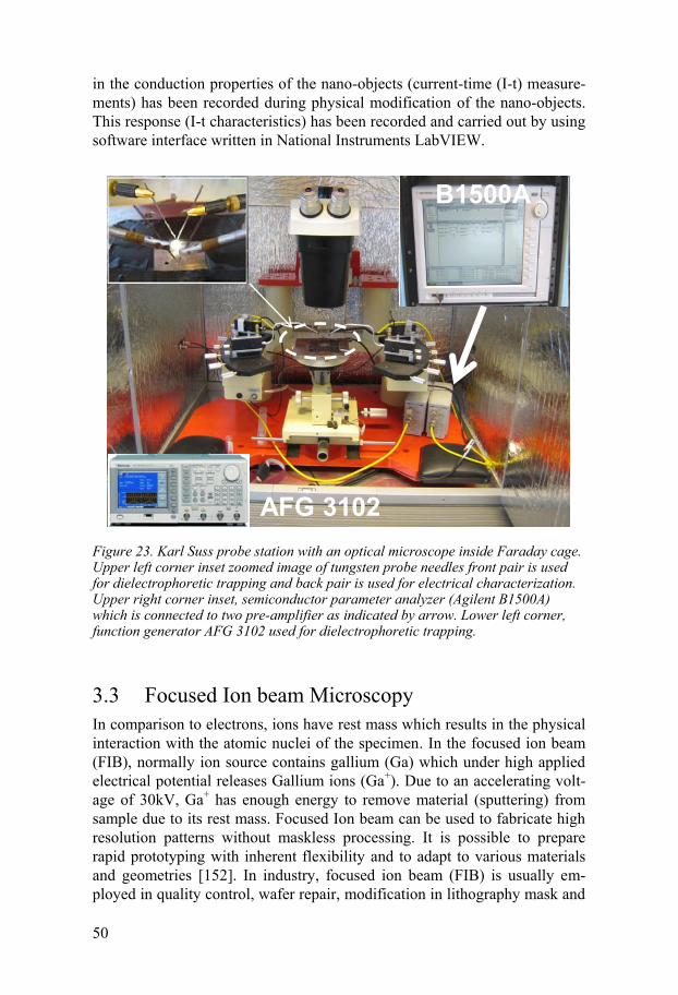
50
in the conduction properties of the nano-objects (current-time (I-t) measure-ments) has been recorded during physical modification of the nano-objects. This response (I-t characteristics) has been recorded and carried out by using software interface written in National Instruments LabVIEW.
Figure 23. Karl Suss probe station with an optical microscope inside Faraday cage. Upper left corner inset zoomed image of tungsten probe needles front pair is used for dielectrophoretic trapping and back pair is used for electrical characterization. Upper right corner inset, semiconductor parameter analyzer (Agilent B1500A) which is connected to two pre-amplifier as indicated by arrow. Lower left corner, function generator AFG 3102 used for dielectrophoretic trapping.
3.3 Focused Ion beam Microscopy In comparison to electrons, ions have rest mass which results in the physical interaction with the atomic nuclei of the specimen. In the focused ion beam (FIB), normally ion source contains gallium (Ga) which under high applied electrical potential releases Gallium ions (Ga+). Due to an accelerating volt-age of 30kV, Ga+ has enough energy to remove material (sputtering) from sample due to its rest mass. Focused Ion beam can be used to fabricate high resolution patterns without maskless processing. It is possible to prepare rapid prototyping with inherent flexibility and to adapt to various materials and geometries [152]. In industry, focused ion beam (FIB) is usually em-ployed in quality control, wafer repair, modification in lithography mask and
AFG 3102
B1500A

51
microelectronics failure analysis [153]. In the laboratory environment, FIB is mostly used to prepare TEM samples [154]. Gallium ions are also used to deposit material by decomposing metal-organic gases and this technique is known as ion beam induced deposition (IBID). These gases are injected into the chamber using special gas injection system (GIS) that injects metal-organic gases very near to substrate in a vacuum chamber. Metal organic gas diffuses and adsorbs on the sample surface. The adsorbed gas molecules are broken down with high energy ions, which in turn deposit platinum atoms on the sample surface and the remaining gas is sucked away into vacuum. Gal-lium ions can also be used to image samples as ion-sample interactions gen-erate secondary electrons. The advantage of imaging with ions is less charg-ing of the sample but continuous irradiation of ions will result in sputtering of the sample surface. In this thesis, FEI Strata DB235 FIB/SEM equipped with a field emission gun (FEG) was used, installed with ion beam and elec-tron beam at 520 to each other allow patterning if the specimen with ion beam and image with electron beam as shown in Figure 24.
Figure 24. Camera photos of the FEI Strata DB235 FIB/SEM and (inset upper left corner) Electron beam column and ion beam column inside the FIB/SEM chamber.
Other advantages of E-beam column in a dual beam microscope is acquisi-tions of 3D high resolution images of a sample by slicing it with focused ion beam and imaging with the electron beam at each slicing step. Electron beam contains electrons that have enough energy to decompose metal-organic gases and deposit material, this technique is known as electron beam induced
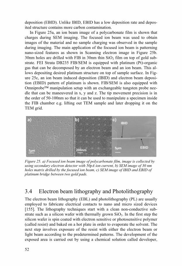
52
deposition (EBID). Unlike IBID, EBID has a low deposition rate and depos-ited structure contains more carbon contamination.
In Figure 25a, an ion beam image of a polycarbonate film is shown that charges during SEM imaging. The focused ion beam was used to obtain images of the material and no sample charging was observed in the sample during imaging. The main application of the focused ion beam is patterning nano-sized features as shown in Scanning electron image in Figure 25b. 30nm holes are drilled with FIB in 30nm thin SiO2 film on top of gold sub-strate. FEI Strata DB235 FIB/SEM is equipped with platinum (Pt)-organic gas that can be decomposed by an electron beam and an ion beam. This al-lows depositing desired platinum structure on top of sample surface. In Fig-ure 25c, an ion beam induced deposition (IBID) and electron beam deposi-tion (EBID) pattern of platinum is shown. FIB/SEM is also equipped with Omniprobe™ manipulation setup with an exchangeable tungsten probe nee-dle that can be maneuvered in x, y and z. The tip movement precision is in the order of 50-100nm so that it can be used to manipulate a specimen inside the FIB chamber e.g. lifting out TEM sample and later dropping it on the TEM grid.
Figure 25. a) Focused ion beam image of polycarbonate film, image is collected by using secondary electron detector with 50pA ion current, b) SEM image of 30 nm holes matrix drilled by the focused ion beam, c) SEM image of IBID and EBID of platinum bridge between two gold pads.
3.4 Electron beam lithography and Photolithography The electron beam lithography (EBL) and photolithography (PL) are usually employed to fabricate electrical contacts to nano and micro sized devices [155]. The lithography techniques start with a clean non-conductive sub-strate such as a silicon wafer with thermally grown SiO2. In the first step the silicon wafer is spin coated with electron sensitive or photosensitive polymer (called resist) and baked on a hot plate in order to evaporate the solvent. The next step involves exposure of the resist with either the electron beam or light beam according to the predetermined patterns. The development of the exposed area is carried out by using a chemical solution called developer,
200nmEBID
IBID
5µm1µm
a) b) c)
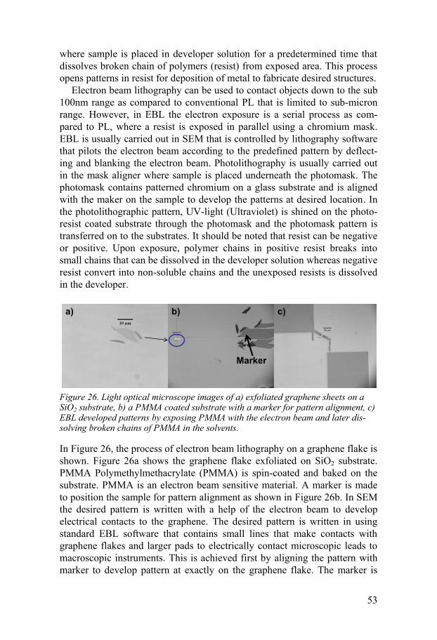
53
where sample is placed in developer solution for a predetermined time that dissolves broken chain of polymers (resist) from exposed area. This process opens patterns in resist for deposition of metal to fabricate desired structures.
Electron beam lithography can be used to contact objects down to the sub 100nm range as compared to conventional PL that is limited to sub-micron range. However, in EBL the electron exposure is a serial process as com-pared to PL, where a resist is exposed in parallel using a chromium mask. EBL is usually carried out in SEM that is controlled by lithography software that pilots the electron beam according to the predefined pattern by deflect-ing and blanking the electron beam. Photolithography is usually carried out in the mask aligner where sample is placed underneath the photomask. The photomask contains patterned chromium on a glass substrate and is aligned with the maker on the sample to develop the patterns at desired location. In the photolithographic pattern, UV-light (Ultraviolet) is shined on the photo-resist coated substrate through the photomask and the photomask pattern is transferred on to the substrates. It should be noted that resist can be negative or positive. Upon exposure, polymer chains in positive resist breaks into small chains that can be dissolved in the developer solution whereas negative resist convert into non-soluble chains and the unexposed resists is dissolved in the developer.
Figure 26. Light optical microscope images of a) exfoliated graphene sheets on a SiO2 substrate, b) a PMMA coated substrate with a marker for pattern alignment, c) EBL developed patterns by exposing PMMA with the electron beam and later dis-solving broken chains of PMMA in the solvents.
In Figure 26, the process of electron beam lithography on a graphene flake is shown. Figure 26a shows the graphene flake exfoliated on SiO2 substrate. PMMA Polymethylmethacrylate (PMMA) is spin-coated and baked on the substrate. PMMA is an electron beam sensitive material. A marker is made to position the sample for pattern alignment as shown in Figure 26b. In SEM the desired pattern is written with a help of the electron beam to develop electrical contacts to the graphene. The desired pattern is written in using standard EBL software that contains small lines that make contacts with graphene flakes and larger pads to electrically contact microscopic leads to macroscopic instruments. This is achieved first by aligning the pattern with marker to develop pattern at exactly on the graphene flake. The marker is
Marker
a) b) c)
54
located in SEM with an electron beam with quick scanning at lower magni-fication that keeps the electron dosage below the threshold level that is re-quired for the breakage of polymer chains in spin coated and baked PMMA. After aligning the pattern inside SEM, it is printed on the substrate by using the electron beam. The electron dose during exposure is controlled to avoid over exposure or under exposure by controlling the electron beam exposure time for a particular electron beam current. The sample is later developed by placing it for 1 minute in the mixture solution (1:3) of Methyl Isobutyl Ke-tone (MBK) and Isopropanol (IPA) to dissolve the broken chains of poly-mer. The sample was washed by placing it in IPA solution for 45 seconds. Figure 26c shows developed EBL pattern after exposure of the PMMA with electron beam and development of exposed electron beam area.
After development of the patterns, the metallization is carried out to place electrical contact on top of the sample. This process is usually done by elec-tron beam and/or resistive evaporation. Resistive evaporation of metal (gold) is carried out by placing it on a conductive substrate i.e. tungsten. Large current up to 50-60 amperes is passed through the conductive substrate to evaporate gold by the resistive heating on to the developed pattern. In e-beam evaporation, electrons emitted from the tungsten filament are focused on the metal and the energy transferred from electrons evaporates the metal. Evaporated metal condensates and forms a thin film on the substrate with developed pattern. In this thesis, patterns are generated on SiO2 and a thin layer of chromium is used as a adhesion layer between the substrate and gold. A 3-5nm thick layer of chromium is deposited by the e-beam evapora-tion on the generated patterns that was followed by a resistive evaporation of gold on to the substrates. In the final step, the substrate was placed in ace-tone for few hours for the removal of the deposited metal on top of the unde-veloped polymer on the sample. Washing with acetone removed the unde-veloped polymer and the metal remained only on the patterns generated by lithography.
3.5 Fabrication of the nanoelectrode platform The nanoelectrode platform is fabricated as described in Ref. [108], a brief summary of the process is described below. The nanoelectrode platform is prepared on a silicon dioxide (SiO2) substrate. The 1µm thick SiO2 is ther-mally grown by oxidation of silicon wafers. It is then broken down into smaller pieces of approximate 2 cm x 2cm size.

55
3.5.1 Fabrication of contact electrodes by Electron beam lithography
These wafers are coated with an electron beam sensitive resist. PMMA 495k A4 as bottom layer and PMMA 950k A4 as top layer are spin coated at 5000 rpm. These wafers are heated at 170O C for 1 minute to remove solvents from PMMA. The electron beam lithography is carried out in the ESEM/electron beam lithography FEI XL30 operating at 30kV using Na-nometer Pattern Generation System (NPGS), where the desired pattern is drawn in computer aided design file.
Figure 27. SEM images of the center part of the EBL pattern after metal deposition and lift-off a) straight line b) crossbar structure. Scale bar is 500 nm.
Typically 96 patterns, each 130µm long, 5-10µm wide in sides and 200 nm narrow in center are written on electron beam sensitive resist. The 8 groups are each 2.5nm apart. The narrow central part of the pattern is shown in Fig-ure 27a. A few cross bar patterns are also written to prepare the sided-gated setup as shown in Figure 27b. A group consists of 12 pattern spaced by 200µm as shown in Figure 28. In order to develop EBL pattern, the exposed PMMA resist is developed in 1:3 MIBK:IPA for 1 min and rinsed in pure IPA for 45s. Light optical microscope (Olympus AX70) is used to check the developed pattern. Then a 3nm thick layer adhesion layer of chromium is deposited using e-beam metal evaporation and 50-70nm thick gold layer is deposited by resistive evaporation (Figure 27). The stripping of PMMA is done by washing sample with acetone and IPA.
3.5.2 Fabrication of macro-contact pads by photolithography In order to bridge the gap between nano levels to macro levels, large con-tacts pads are developed by photolithography technique. Fabrication of larg-er gold pad makes it easy to make stable electrical contacts either by probe needles in probe station or by wire bonding. Photo resist is spin coated using
a) b)

56
spin coater - BLE Delta 20. Photolithography is carried out by using chromi-um mask in the mask aligner - Karl Süss MA6. Patterns are developed in developer solution and checked using light optical microscope. Metal depo-sition is again carried out by depositing 3nm Cr and 250-300nm gold. Gold contact pads are made thicker to withstand the scratching from the probe needles and as well as wire-bonding process. SEM images in Figure 28 show larger pads that are contacted with EBL developed structure along with 12 contacts in parallel form a single group. Figure 28b shows top view of a single nanoelectrode platform with micro-sized contact pads as observed in SEM.
Figure 28. SEM images of nanoelectrode after the photolithography, metal deposi-tion and lift-off steps. a) Two groups of nanoelectrodes having 12 nanoelectrodes in parallel. b) Zoomed view of single nanoelectrode where central part is developed by electron beam lithography and larger contact pads are fabricated by photolithogra-phy.
The nanoelectrode platform was involved in experiments carried out in pa-per IV-XI. However in paper XI, low temperature measurements have been carried out. In order to carry out such measurement nanoelectrodes were fixed inside the chip holder that can be inserted inside liquid helium based electrical measurement testing setup. This step should be carried out before cutting the EBL developed gold contacts because these nanoelectrodes are very sensitive and slight charging of one of the electrode leads to broken nanoelectrodes.
As shown in Figure 29, samples were fixed in chip holder of size 1cmx1cm. Sample with eight groups of 12 nanoelectrodes were broken down into a single group of 12 nanoelectrodes. It was then fixed into chip holder by heating the chip holder to 250oC and soldering the sample to it with the help of soldering wire. Ball wire bonding was carried out using Kulicke&Soffa 4522 to electrically contact 9 nanoelectrodes to 18 pins of the chip holder, whereas one pin was used to ground the substrate to reduce capacitive effect between nanoelectrodes and substrate. Very low power and frequency with the long pressing times were used to avoid SiO2 breakdown in between gold contact pads and the substrate. However, impedance (Z) measurements with frequency sweep (1 kHz to 1 MHz) were carried out after wire-bonding to determine SiO2 breakdown during wire-bonding.
1 mm
a) b)

57
Figure 29. a) Light optical microscope image of nanoelectrodes fixed and wire bond in chip holder. b) SEM image of wire bonded nanoelectrodes on silicon substrate to the chip holder for immersing sample in liquid helium measurement setup.
3.5.3 Milling of electrodes using focused ion beam In order to fabricate gap in between EBL developed line, dual beam FIB/SEM FEI Strata DB235 was used with Ga+ ion beam operating at 30kV. For a small gap size, the ion beam needs to be aligned perfectly and should be focused properly with lowest possible ion beam current (1 pA) to achieve smaller beam size. Furthermore, to reduce the beam size, emission currents from Ga+ ion source (default value: 2.2µA) is reduced to ~1.0µA.
Figure 30. a) SEM image of the of test lines, cut by 1pA ion beam at 30kV using emission currents of 1.0 µA with varying milling time (50% overlap and 1µs dwell time). b) SEM image of <20nm gap (right) with milling time of 1.2 s. The small particles in the vicinity of the gap originated from the sputtering process. The larger particles in the lower part of the image come from the Au deposition and the lift-off step.
500µm
a) b)
200nm1.1s1.3s1.5s1.7s1.9s
100nm
a) b)

58
Ion beam was aligned by digging a hole of 0.5µmx0.5µm in the SiO2 sub-strate at higher ion current next to the EBL developed gold wire. This hole was imaged with 1pA current to adjust focus and stigmation. The ion beam was fine focused and adjusted for stigmatism on edges of the hole. Initially, 1µm long test cuts with varying milling times were made on gold surfaces using 50% overlap and the dwell time of 1µs (Figure 30a). After choosing the proper milling time, ion milling was carried out on EBL developed line as shown in Figure 30b. Full batch of nanoelectrodes are cut following the same procedure one by one. Later I-V characteristics of the single empty nanogap in between nanoelectrode setup were carried out to check the quali-ty of produced nanogaps in a batch. nanogaps demonstrate resistance in or-der of 1000T
Chapter summary Structural characterization techniques have been used extensively throughout this thesis. Light optical microscopy has been employed for quality control during lithography and most importantly to locate thin flakes of graphene on a 300nm thermally grown SiO2 on the silicon substrates. Scanning electron microscopy has been used to image nanoparticles and free standing graphene sheets either after or during the nano-contacting process. Nanoparticles sizes, distance between two nanoparticles and their atomic structure have been determined by TEM. Atomic force microscopy with Ångström resolution has been used to measure thickness of exfoliated graphene sheets on SiO2 and to observe the changes in surface profile of graphene after ion irradia-tion. Raman spectroscopy is used to study the vibration modes of the bonds in molecules and here it has been used to identify a single or a multiple layer graphene sheets. FIB/SEM was extensively used for nano-structuring, nano-contacting and defect creation in graphene in this thesis. Presence of SEM in same chamber allows manipulating sample during structuring and contact-ing.
For electrical characterization, a manual 4 probe station with microma-nipulators has been used to make electrical contacts with advance source meters. Nanoelectrode platforms were prepared by top-down approaches using combined techniques of electron-beam lithography, photography and ion beam milling. In this thesis, EBL developed lines were cut by focused ion beam with the gap size of 10-40nm depending on the application. The larger pads for contacting via probe station of wire bonding were prepared by photolithography. The gap resistance of these gaps was in order of 1000-1500T.
59
4 Conduction properties of graphene and defect induced graphene
There is a strong focus on the tailoring of electronic properties by means of defects, ad-atoms and geometrical confinement that will lead to the realiza-tion of incorporation of graphene in electronic devices. The central aspect of this chapter is to determine resistances of defect induced graphene sheet and to observe effect of defect on conductivity of graphene. In section 4.1, theo-retical prediction regarding introduction of defects in graphene lattices is presented. Experimentally these defects are created by chemical means i.e. by the acid treatment (section 4.2) as well as by physical means i.e. by the sputtering using gallium ions at 30kV (Section 4.3).
4.1 Conduction properties of graphene with defects To establish graphene as a competitive material for the next generation elec-tronics, the fundamental steps are to open the bandgap, induce mid-gap states and ability to control conductivity of graphene [156]. In order to ob-serve the effect of vacancy defect on electronic properties of graphene, both single vacancy and di-vacancy are introduced in the л bonded graphene structure through a tight-bonding model with nearest neighbor interaction (Paper I). Vacancy induces mid-gap states that arise due to symmetry break-ing, which removes the equivalent Dirac points in the two sub-lattices. Di-vacancy defects induce mid-gap states in both sub-lattices A and B, which results in graphene becoming metallic in the neighborhood of the defect and this metallicity around the defects extends over a few lattice parameters. Graphene conductivity was calculated by using an all electron scalar- relativ-istic version of the tight-binding linear mufin-tin orbital (TB-LMTO) method [157] within the local spin-density approximation [158] (LSDA) to the den-sity functional theory [159]. Ab-initio calculations had been carried out to calculate the conductance of graphene as a function of vacancy defect as shown in Figure 31. As concentration of defects increase the resistivity de-crease by two orders of magnitude. In the regime when defect concentration is less than 0.005, the conductivity increases exponentially with respect to defect concentration. This is due to the transition from a semi-metallic re-gime (or Zitterbewegung dominate regime) with limited conductivity [36,

60
160], to a regime of highly conducting graphene, which is driven by defects via the creation of mid-gap states resulting in extended regime of metallic character. However, above 0.005 defect concentration resistivity slightly increases as more defects produce scattering centers, resulting in the conven-tional behavior (Paper I).
Figure 31. Calculated resistance of a single graphene layer as the function of de-fects concentration, the red diamond represents a calculated resistance from a mod-el consideration with a low amount of defects but a relatively large shift of the Fer-mi level. (Adopted from Paper I and reproduced by the permission of IOP)
4.2 Defects in graphene induced by chemical means Graphene can be prepared by mechanical exfoliation, chemical vapor depo-sition (CVD) process and wet chemistry synthesis. High concentration acid treatment at elevated temperature is required to create vacancy defects in graphene. Acid treatment of exfoliated graphene on silicon substrate results in additional reaction of acid with the SiO2 substrate, making it impossible to observe the effect of vacancy defects due to charging and impurities from processing. In order to avoid artifacts, free standing graphene sheets (Paper I and II) consisting of few layers of graphene with monolayer and double layer at the edge are used. These sheets are grown by plasma-assisted chemi-cal vapor deposition (PACVD) on tungsten substrate, which provides back contact to sheets (Figure 32a and 32b). These sheets consist of 1µm long graphene sheets protruding from a 20 nm layer of graphite [161]. The sche-matic illustration of these sheets is shown in Figure 32c. Ultimately, free standing graphene sheets allow both wet chemical treatment [162] and point contact measurements without the adverse effects associated with removal of the graphene sheets from the substrate and the deposition and subsequent electrical contacting using electron beam lithography.

61
Figure 32.a,b) SEM images of PACVD grown graphene nanosheets on top of tung-sten substrate c) Schematic illustration of free standing graphene sheets. (adopted from Paper I and published with the permission from IOP)
The defects were introduced in the free standing graphene sheets by a treat-ment with the concentrated aqueous hydrochloric acid (HCl) as described [162], the free standing graphene sheets were exposed to 35% concentrated aqueous HCl at 363K for 3 hours. The HCl was removed from the flasks using a pipette and the samples were treated with deionized water for 10 h at 363K, followed by a thorough rinse with deionized water at ambient condi-tion and drying in air at 423K for 3 min.
4.2.1 Measurement setup In order to characterize these graphene nanosheets an in-situ electrical char-acterization without any processing of the sample is carried out (Paper II). This system can be used for a large quantity of micro- and nano-sized ob-jects giving a large number of measurements, i.e. excellent statistics. This technique is employed in FEI Strata DB235 equipped with an Omniprobe manipulator and the schematic of this setup is shown in Figure 33a. The manipulator as well as the sample stage inside the chamber is connected to a 2-to-1 BNC connector outside the chamber. This is to connect the manipula-tor and the sample stage to the preamplifier on a Keithley 6430 source-meter. The source-meter is controlled by a computer in order to perform the measurements and record the results. The Omni-probe needle, used here for contacting graphene nanosheets flakes, is made of tungsten with a radius of curvature of about 500nm in their original state. The tip of the needle is too large to contact single nano-object precisely as shown in Figure 33b and tungsten surface might be oxidized during storage in ambient condition. The tip of needle is sharpened (Paper II) by using sputtering ion beam to make electrical contact with single graphene sheet. After fine polishing, the radius of the tip is reduced to 20nm and can contact a single free standing graphene sheet (Figure 33c).
1µm1µm
a) b)
~1 μm
Substrate
1-7 Graphene layers
20 nm
Edge
Bulk layer
Surface layer
c)

62
Figure 33 a) Schematic illustration of the experimental measurement setup where the source-meter is connected to the manipulator tip as well as to the sample holder and finally to a PC for recording the measurements (Adopted from Paper II and reproduced by the permission of APS). SEM images of the a) unsharpened tungsten and b) sharpened tip put into contact with a 52 single carbon nanosheet. The sample is tilted to 52° with respect to the electron beam.
Contact resistance also plays a vital role in measuring nano-objects. The unsharpened needle-gold junction has demonstrated resistance in order of 70k due to the presence of barrier related to surface oxide layer covering tungsten (W) surfaces. However the sharpened tip-gold interface is found to have a contact resistance of 10This result demonstrates that sharpening of the needle not only allows making contact with nano-objects, but also reduc-es contact resistance by removing oxide layer from surface. In addition to that, the leakage current including electrical noise inside the FIB/SEM chamber is in range of 10pA range, which allows us to characterize devices up to 0.1T range, thus making this technique also suitable for semiconduc-tor devices.
4.2.2 Electrical characterization of graphene nanosheets In this nano manipulation setup, the probe needle was maneuvered in the x, y and z-direction in real time to contact with top of the graphene nanosheets as shown in Figure 33c. I-V sweeps were carried out from -1V to 1V. SEM images were taken before and after I-V sweep to compare contact and ob-serve temporary detachment of the tip due to occasional drift and tip vibra-tions. In case of detachment, measurement was discarded for further evalua-tion.
Six different samples prepared in two batches (A and B) were electrical contacted and characterized. In batch A, defects were created in one sample
1µm
b)
1µm
c)
SOURCE METER
b) ElectronB
eam
FIB\SEM Chamber
Pre-amplifier
To PC
In-House built 2-1 BNC Connector
a)
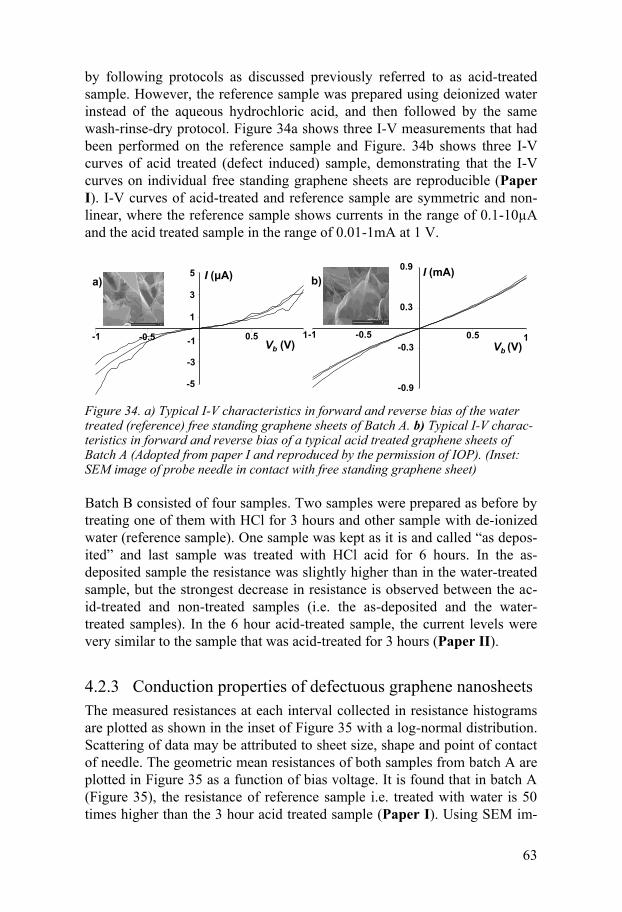
63
by following protocols as discussed previously referred to as acid-treated sample. However, the reference sample was prepared using deionized water instead of the aqueous hydrochloric acid, and then followed by the same wash-rinse-dry protocol. Figure 34a shows three I-V measurements that had been performed on the reference sample and Figure. 34b shows three I-V curves of acid treated (defect induced) sample, demonstrating that the I-V curves on individual free standing graphene sheets are reproducible (Paper I). I-V curves of acid-treated and reference sample are symmetric and non-linear, where the reference sample shows currents in the range of 0.1-10µA and the acid treated sample in the range of 0.01-1mA at 1 V.
Figure 34. a) Typical I-V characteristics in forward and reverse bias of the water treated (reference) free standing graphene sheets of Batch A. b) Typical I-V charac-teristics in forward and reverse bias of a typical acid treated graphene sheets of Batch A (Adopted from paper I and reproduced by the permission of IOP). (Inset: SEM image of probe needle in contact with free standing graphene sheet)
Batch B consisted of four samples. Two samples were prepared as before by treating one of them with HCl for 3 hours and other sample with de-ionized water (reference sample). One sample was kept as it is and called “as depos-ited” and last sample was treated with HCl acid for 6 hours. In the as-deposited sample the resistance was slightly higher than in the water-treated sample, but the strongest decrease in resistance is observed between the ac-id-treated and non-treated samples (i.e. the as-deposited and the water-treated samples). In the 6 hour acid-treated sample, the current levels were very similar to the sample that was acid-treated for 3 hours (Paper II).
4.2.3 Conduction properties of defectuous graphene nanosheets The measured resistances at each interval collected in resistance histograms are plotted as shown in the inset of Figure 35 with a log-normal distribution. Scattering of data may be attributed to sheet size, shape and point of contact of needle. The geometric mean resistances of both samples from batch A are plotted in Figure 35 as a function of bias voltage. It is found that in batch A (Figure 35), the resistance of reference sample i.e. treated with water is 50 times higher than the 3 hour acid treated sample (Paper I). Using SEM im-
I (mA)
Vb (V)
-0.9
-0.3
0.3
0.9
-1 -0.5 0.5 1
-5
-3
-1
1
3
5
-1 -0.5 0.5 1Vb (V)
I (μA)a) b)

64
ages of samples from batch A, average surface area is estimated. Reference sample has a resistivity 150 µ-Wm, whereas resistivity of acid treated sam-ple is 3.5µ-Wm. Reference sample has same resistivity as nano-crystalline graphite [163] with the crystal size of 2-5nm, which is in accordance to structure of these sheets [164]. Water treated and 3 hour acid treatment of batch B demonstrates similar behavior as measured in case of batch A as (Paper II). However, resistance of the as-treated sample is higher than the reference sample, which may be attributed to residue from PECVD process removed during washing of the sample. 6 hour acid treatment sample has slightly lower resistance than 3 hour acid treated sample. It might indicate the defect saturation.
Figure 35. Resistance (log scale) vs. applied voltage in approx. 100 measurements (both forward and reverse bias are included) of reference (upper curve, solid line) and acid treated sample (lower curve, dotted line) (Adopted from paper I and repro-duced by the permission of IOP). Inset: log-normal histograms of resistances meas-ured in typical free standing graphene sheets at 0.3V of the a) reference sample of Batch A and b) acid treated sample of Batch A.
It is concluded that chemical treatment of these sheets can be used to tune conductance of graphene with more than one order of magnitude. Conductiv-ity measurements show that the acid treatment has modified the graphene structure. Such structural modification could be nucleated at step edges pre-sent in high density (the graphene thickness changes between 1-7 monolay-ers) and at the grain boundaries. The observation of defects in acid-treated free standing graphene sheets by x-ray spectroscopy measurement [162]
Res
ista
nce
()
Voltage bias (V)
103
104
105
106
0 0.1 0.2 0.3 0.4 0.5 0.6 0.7
Reference Sample Acid Treated Sample
a) b)

65
indicates that the decrease in resistance of these sheets is related to the de-fects created during the acid treatment.
Figure 36. a) Schematic illustration of measurement setup where electrically con-nected graphene flakes are bombard with controlled dose of Ga+ ions and imaged via electron beam after each irradiation, b) camera image of a substrate on the cryogenic stage inside FIB/SEM, c) light optical image of a graphene device with extended contacts and gold leads (exfoliated graphene on SiO2 substrate with gold contacts developed by electron beam lithography). Adopted from paper III
4.3 Defects in graphene induced by physical means The general idea behind is to create defects in electrically connected gra-phene sheets by removal of carbon atoms either by using high energy elec-tron beam in TEM [165] or by using the low and the high energy ion beams. In this thesis, contacted graphene flakes on SiO2 substrate have been irradi-ated with controlled dose of 30kV Gallium ions (Ga+). In-situ electrical and structural characterizations of graphene during ion beam damaging have been carried out (Paper III). The similar experiments have been conducted at liquid nitrogen temperature inside FIB/SEM using cryogenic setup.
4.3.1 Measurement Setup Thin sheets (1-4 layers) of graphene have been produced on 300nm thick SiO2 substrate by mechanical exfoliation [35]. Details on graphene exfolia-
2 to 1 BNC connector
Electron beam
Source-meter
Gold wire
Graphene
Ga+
a) b)
c)
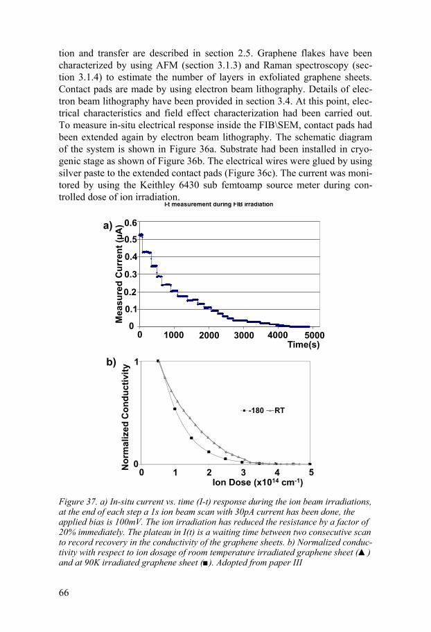
66
tion and transfer are described in section 2.5. Graphene flakes have been characterized by using AFM (section 3.1.3) and Raman spectroscopy (sec-tion 3.1.4) to estimate the number of layers in exfoliated graphene sheets. Contact pads are made by using electron beam lithography. Details of elec-tron beam lithography have been provided in section 3.4. At this point, elec-trical characteristics and field effect characterization had been carried out. To measure in-situ electrical response inside the FIB\SEM, contact pads had been extended again by electron beam lithography. The schematic diagram of the system is shown in Figure 36a. Substrate had been installed in cryo-genic stage as shown of Figure 36b. The electrical wires were glued by using silver paste to the extended contact pads (Figure 36c). The current was moni-tored by using the Keithley 6430 sub femtoamp source meter during con-trolled dose of ion irradiation.
Figure 37. a) In-situ current vs. time (I-t) response during the ion beam irradiations, at the end of each step a 1s ion beam scan with 30pA current has been done, the applied bias is 100mV. The ion irradiation has reduced the resistance by a factor of 20% immediately. The plateau in I(t) is a waiting time between two consecutive scan to record recovery in the conductivity of the graphene sheets. b) Normalized conduc-tivity with respect to ion dosage of room temperature irradiated graphene sheet (▲) and at 90K irradiated graphene sheet (■). Adopted from paper III
I-t measurement during FIB irradiation
0
100
200
300
400
500
600
6300 7300 8300 9300 10300 11300
Time [s]
Cur
rent
[nA
]
0 1000 2000 3000 4000 5000
0.6
0.5
0.4
0.3
0.2
0.1
0Mea
sure
d C
urre
nt (µ
A)
Time(s)
-180 RT
0 1 2 3 4 5
1
0Nor
mal
ized
Con
duct
ivity
Ion Dose (x1014 cm-1)
a)
b)

67
4.3.2 Conduction properties of defect induced graphene Graphene flakes have been irradiated with Ga+ ions with accelerating voltage of 30kV. A scan area of 30x30µm2 was selected which covers the whole flake and extend underneath the substrate. Each scan corresponds to a 1 se-cond ion exposure. The ion current of 26pA with dwell time of 1µs and zero overlap was chosen. The estimated ion dose for a single scan was calculated to be 0.18ions/nm2. In Figure 37a, the in-situ conduction response of a gra-phene sheet during ion irradiation is shown (Paper III). With every scan, immediately the resistance of flakes decreased by almost 20%. Succeeding scan was done after 5-7 minutes to observe any recovery in conduction of graphene. The device resistance increased from 50k to 100M in the scan time of 750s. Graphene demonstrated enhanced resistance to the ion dose and did not sputter completely from the substrate [99]. Raman spectroscopy after the ion dose of 1.16*1012 ions/cm2 demonstrated appearance of D peak in the recorded Raman spectra (Paper III). However, it was observed that after complete disappearance of electrical signal in noise, the remains of the graphene flake indicated the presence of amorphous carbon [101]. The Ga+ ion irradiation also modifies graphene structure where electron conduction changes from diffusion to hopping regime [100]. Similar measurements had been carried out at cryogenic temperature. In Figure 37b, we have plotted normalized variation in graphene resistance with the ion dosage. It can be observed that at cryogenic temperature the graphene resistance decreases quickly as compared to room temperature. This might be an indication of defects in the carbon lattice that can rearrange or recover to a large extent at room temperature as than at cryogenic temperature.
Unlike the acid treated graphene flakes which showed decrease in resis-tivity upon introduction of di-vacancy defects, the ion-irradiated sample demonstrated an increase in resistivity. A difference between the two sys-tems is that in the chemical treated sample, defects in graphene sheets are free from the influence of any other material while in the ion beam exposed sample where defects in exfoliated graphene interacts with underlying SiO2. For example, the ions also sputter SiO2 that might be dispersed on exfoliated graphene sheets and result in creating scattering centers, which lead to de-crease in the conductivity of graphene.
Chapter Conclusions When graphene is to be used as a foundation material to obtain nanomateri-als or components with new mechanical, electrical or optical properties, it is important to tailor the properties of graphene. It is theoretically calculated that conductivity of graphene increases by an order of magnitude with intro-duction of the vacancy defects. The mid-gap states appear due to the di-
68
vacancy defects. These defects introduce metallicity which extends over several lattices. The vacancy defects can be introduced by chemical treat-ment. Chemical treatment has been carried out on free standing graphene sheets as in case of exfoliated graphene sheet, the underlying substrate can introduce artifacts in graphene sheets. An electrical measurement setup has been prepared inside FIB/SEM with a 50nm in-situ sharpened tip. This tip can be moved around and thereby make electrical contact with individual free standing graphene sheets. This technique involves no cleanroom pro-cessing steps and can be used to electrically characterize a number of sheets one after another. It was observed that conduction in an acid treated sample is 50 times more than in the reference sample.
Defects are also created in the exfoliated graphene sheets on SiO2 with an ion irradiation inside FIB/SEM at the room and cryogenic temperatures. The conductivity decreased almost 20% with a single ion beam scan with an ion dosage of 0.18 ions/nm2. At cryogenic temperature the resistance change is higher per dose as compared to room temperature ion irradiation. The de-crease in conductivity in graphene during ion bombardment is due to both the removal of carbon atoms from graphene as well as creation of the scatter-ing centers due to sputtering of the underneath SiO2. The substrate effects have dominated the conduction properties of graphene during ion bombard-ment.
Another interesting question is also, which type of defects the ion bom-bardment creates. With our AFM analysis, we observed that after the ion bombardment, the original graphene flake consists of alternating regions of graphene flakes and 10nm large holes in between the graphene regions (pa-per III). Thus, the original theoretical model, used in paper I which relies on the creation of di-vacancies cannot be applied to these larger defects. Larger defects would consequently lead to a decrease in the conductivity as observed in the ion bombardment experiments on exfoliated graphene.
69
5 Preparation of the nanoelectrode platform for electrical characterization of molecules and nanoparticles
In order to build devices from nanoparticles and molecules, a stable and solid state platform is required that should demonstrate reproducible charac-teristics. Fabricating electrical contacts to nanoparticles and molecules is not a straight forward issue. In order to measure molecules directly, the gap size in between the nanoelectrodes has been reduced to 5nm from 25nm FIB cut gaps by electrodeposition of gold, however 1-2nm gap-size could not achieved due to instability of gold electrodes at the low dimensions (section 5.1) that is required for direct measurement of molecules. Shelf life evalua-tion and stability of gap size in FIB cut nanoelectrode over a period of month in ambient condition, water and organic solvents, are discussed in section 5.2. In our nanoelectrode platform, three clean room technique photolithog-raphy (PL), electron beam lithography (EBL) and focused ion beam (FIB) were used to address the appropriate dimensions and to move from macro-scopic to microscopic to nanoscopic scale. Therefore the use of AuNPs is a logical step to connect the 1-2 nm molecules to the 100-150 nm wide and 15-30nm spaced gold electrodes. Molecules can be introduced in between AuNP-nanoelectrode bridge platform, but it is required to obtained metallic contact between AuNP and nanoelectrode, otherwise junction resistance dominates the molecular conduction properties (section 5.4). A similar ap-proach has been employed to trap semiconductor nanoparticles that demon-strate utility of platform in studying various physical properties of materials like photoconductivity (section 5.5).
5.1 Sub-5nm nano gaps for direct measurements on molecules
In an attempt to reduce the gap size of nanoelectrode setup, an electrochemi-cal route is adopted. Reducing the gap size comparable to the size of mole-cules creates the possibility to trap or place molecule directly inside the gap. In paper IV, preparation of sub 5nm gap with hundreds of T gap re-sistance on FIB cut nanogaps is demonstrated for the first time. The FIB cut
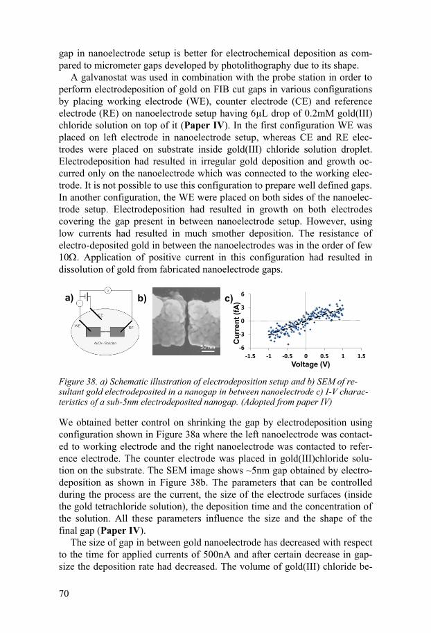
70
gap in nanoelectrode setup is better for electrochemical deposition as com-pared to micrometer gaps developed by photolithography due to its shape.
A galvanostat was used in combination with the probe station in order to perform electrodeposition of gold on FIB cut gaps in various configurations by placing working electrode (WE), counter electrode (CE) and reference electrode (RE) on nanoelectrode setup having 6µL drop of 0.2mM gold(III) chloride solution on top of it (Paper IV). In the first configuration WE was placed on left electrode in nanoelectrode setup, whereas CE and RE elec-trodes were placed on substrate inside gold(III) chloride solution droplet. Electrodeposition had resulted in irregular gold deposition and growth oc-curred only on the nanoelectrode which was connected to the working elec-trode. It is not possible to use this configuration to prepare well defined gaps. In another configuration, the WE were placed on both sides of the nanoelec-trode setup. Electrodeposition had resulted in growth on both electrodes covering the gap present in between nanoelectrode setup. However, using low currents had resulted in much smother deposition. The resistance of electro-deposited gold in between the nanoelectrodes was in the order of few 10. Application of positive current in this configuration had resulted in dissolution of gold from fabricated nanoelectrode gaps.
Figure 38. a) Schematic illustration of electrodeposition setup and b) SEM of re-sultant gold electrodeposited in a nanogap in between nanoelectrode c) I-V charac-teristics of a sub-5nm electrodeposited nanogap. (Adopted from paper IV)
We obtained better control on shrinking the gap by electrodeposition using configuration shown in Figure 38a where the left nanoelectrode was contact-ed to working electrode and the right nanoelectrode was contacted to refer-ence electrode. The counter electrode was placed in gold(III)chloride solu-tion on the substrate. The SEM image shows ~5nm gap obtained by electro-deposition as shown in Figure 38b. The parameters that can be controlled during the process are the current, the size of the electrode surfaces (inside the gold tetrachloride solution), the deposition time and the concentration of the solution. All these parameters influence the size and the shape of the final gap (Paper IV).
The size of gap in between gold nanoelectrode has decreased with respect to the time for applied currents of 500nA and after certain decrease in gap-size the deposition rate had decreased. The volume of gold(III) chloride be-
-6
-3
0
3
6
-1.5 -1 -0.5 0 0.5 1 1.5
Voltage (V)
c)
Cur
rent
(fA)
a) b)

71
tween the electrodes had decreased that led to decrease in the number of the gold ions. Growth perpendicular to gap had increased nonlinearly due to availability of gold ions in the close vicinity of gold electrodes. The I-V characteristics of sub 5nm gap are plotted in Figure 38c. The measured re-sistances of nanoelectrodes (average size 25nm) before electrodeposition is found to be 1000-1500T The resistance of the gap shown in Figure 38b from linear fit was found to be in order of 300T which is 3 to 4 times less than resistance of original FIB cut gap. However, gap size comparable to the molecules length i.e. 1-2nm is not achieved and hence these gap are not fur-ther used in this thesis.
5.2 Shelf-life of nanogaps in air, water and organic solvents
For a device application, it is extremely important to demonstrate the stabil-ity of nanoelectrode platform over a period of time. It is also important to observe that change in device resistance over the period of time due to the nano-objects structural degradation or the structural changes in the gap size between the nanoelectrodes. A series of experiments on stability of the nanogap in the nanoelectrode platform, gap size and shape in nanoelectrode platform in different storage conditions have been carried out (Paper V). Nanoelectrode platforms were stored in ambient conditions, de-ionized water (polar inorganic solvent), toluene (non-polar, organic solvent), tetrahydrofu-ran (THF, polar organic solvent) and Tetramethylethylenediamine (TMEDA, ligand for metal ion) over a period of one month.
Figure 39. SEM images of nanoelectrodes stored in ambient conditions a) after cutting and b) after four week (scale bar is 100nm. (Adopted from Paper V)
In Figure 39, time evolution of gold nanoelectrodes after four weeks in am-bient conditions is shown, where the gap size in between nanoelectrode had decreased. There was also observable contamination (organic and inorganic) in SEM images. Nanoelectrodes in ambient conditions had demonstrated 2% to 25% change in gap size after 4 weeks. Similarly nanoelectrodes stored in TMEDA had demonstrated 3% to 26% increase in gap size after 4 weeks.
a) b)

72
However the largest increase in gap size had been observed when nanoelec-trodes were stored in THF. The nanogap in between nanoelectrode had demonstrated 18% to 31% increase in the gap size (Paper V). However no prominent change in size of nanoelectrodes was observed when stored in water but contaminations were visible in SEM images taken after 28 days. Time evolution of gold nanoelectrode for four weeks in toluene is shown in Figure 40. No change in size of nano-electrodes was observed, in addition to that there was no observed contamination on the gold nanoelectrodes. The time evolution in 5 nanoelectrodes in toluene was recorded for four weeks and only in gap-size in one nanoelectrode was changed by 3%.
Figure 40. SEM images of nanoelectrodes stored in toluene a) after cutting and b) after four week (scale bar is 100nm). (Adopted from paper V)
The change in gap size in between the nanoelectrodes in ambient conditions can be attributed to the self-diffusion of gold atoms. Due to protic nature, water molecules can form an infinite network of hydrogen bonded water molecules over the gold nanoelectrodes surface which restricts the move-ment of gold atoms. In contrast, there is no interaction between TEMDA molecules and they contain NH anchor groups that can etch away gold from nanoelectrodes. Due to the aprotic nature of THF, the solvent molecules do not interact with each other and make it easier for gold atoms to move on the nanoelectrode surfaces. In comparison, toluene solvent molecules stabilize the gold surface as they can arrange themselves on top of gold surface in π- stacking (layer structure) making it difficult for gold atoms to move around. In conclusion it is found that the gold nanoelectrodes can be stored for a long period of time in toluene without changing the electrode spacing but before trapping the nanoelectrode platform must be washed rigorously with ethanol to remove toluene molecules from the gold surfaces and finally with di-ionized water.
5.3 Dielectrophoretic trapping of metallic nanoparticles
After cutting the gaps, to remove organic contamination, gentle oxygen plasma cleaning is carried out using Plasmastripp Tepla 300. The cleaning
a) b)

73
procedure is carried out by UV/ozone plasma cleaning for 20 minutes before dielectrophoretic trapping of AuNPs in between nanoelectrode. After plasma cleaning nanoelectrodes are kept in 99.9% ethanol solution to remove gold oxide [166].
Figure 41. Schematic illustration of the electrical circuit used for dielectrophoretic trapping of AuNPs in between nanoelectrodes.
Prior to dielectrophrosis trapping, the electrodes were rinsed with de-ionized water and blow dried by nitrogen. Washing with de-ionized water remove charges accumulated on the gold pads. Micro-manipulators moving probe needles inside probe-station are used to contact the larger contact pads on substrate as illustrated in Figure 41. It is suggested to ground both needles on same dummy pad to discharge accumulated charge in circuit to reduce chances of gap destruction this is done before contacting nanoelectrodes.
Figure 42. SEM images of dielectrophoretically trapped AuNPs in between nanoe-lectrode using setup described in Figure 40 a) single AuNP b) 5 AuNPs c) 8 AuNPs in between nanoelectrodes (Scale bar is 30nm)
After placing probe needles on contact pads on top of gold contact pads, a 10µL of droplet of AuNPs solution is poured with the help of a micropipette on top of nanoelectrodes. An alternating voltage of between 1-2 V at the frequency of 1MHz for 30s-60s is applied. A 10 M resistor is placed in series to reduce excessive currents to maximum level of 100-200nA that could lead to fusing of the trapped AuNPs. In order to remove the excessive drop of AuNP solution, the sample is washed with de-ionized water and
SiSiO2
10µL Nanoparticles Dispersion
Micro-manipulator
Function generatorTektronix AFG3102
R=1
0M
Probe-needle
Nanoelectrode Platform
a) b) c)

74
blow dried with nitrogen. The trapping process is repeated on all nanoelec-trodes on a single substrate and immediately I-V characterization is carried out using Agilent 1500B. During trapping attempts, single or multiple AuNPs have been trapped in a nanogap in between the nanoelectrodes re-peatedly by the dielectrophrosis process (Paper V, VI, VIII-XI,). Dielectro-phoretic trapping of semiconductor nanoparticles have been carried out in paper VII. Dielectrophoretic trapping of 30nm AuNPs (BBI international) in between nanoelectrodes are shown in Figure 42. These AuNPs are elec-trostatically stabilized and dispersed in water.
5.4 Control of junction resistance in between nanoelectrodes and metallic nanoparticles
I-V characteristics of trapped AuNPs in between the clean nanoelectrodes demonstrated a linear response. However, resistances of these devices were above 1G. In literature, resistance of AuNPs in nanoelectrode gaps is found to be in order of few M [107]. This indicates the absence of metallic contact between nanoelectrodes and AuNPs, whereas a quantum conduct-ance should be observed in metallic contacts when linked by single gold atoms.
Figure 43. a) I-V characteristics of trapped eight 30 nm AuNPs from 6µL of stock solution in-between gold nano-electrodes. (Inset, SEM image of the device, adopted from paper VI and reproduced by the permission of IOP) b)TEM image of 30nm AuNPs from solution stored in fridge (inset) digitally zoomed interface between two AuNPs.
I-V characteristics as shown in Figure 43a demonstrate device resistance in order of 3.3G (Paper VI). High resistance in metal-metal junction indi-cates the presence of the non-conductive barrier. In order to observe this barrier, transmission electron microscopy of AuNPs was carried out in JEOL 2000FX at 200kV. As shown in Figure 43b, contamination is observable in vicinity of junctions in between AuNPs. In light of these results, nanoelec-
0 25 50-25-50-20
-10
0
10
20
Voltage bias (mV)
Cur
rent
(pA
)
100nm
a) b)
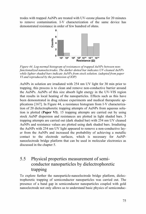
75
trodes with trapped AuNPs are treated with UV-ozone plasma for 20 minutes to remove contamination. I-V characterization of the same device has demonstrated resistance in order of few hundred of ohms.
Figure 44. Log-normal histogram of resistances of trapped AuNPs between non-functionalized nanoelectrodes. The darker dotted bar indicates UV-cleaned AuNPs while lighter shaded bars indicate AuNPs from stock solution. (adopted from paper VI and reproduced by the permission of IOP)
AuNPs in solution are irradiated with 254 nm UV light for 30 min prior to trapping, this process is to clean and remove non-conductive barrier around the AuNPs. AuNPs of this size absorb light energy in the UV-VIS region that results in local heating of the nanoparticles. Effects such as this have been demonstrated in drug release experiments and medical therapeutic ap-plications [167]. In Figure 44, a resistance histogram from I-V characteriza-tion of 20 dielectrophoretic trapping attempts of AuNPs from aqueous solu-tion is plotted (Paper VI). 15 trapping attempts are carried out by using stock AuNP dispersion and resistances are plotted in light shaded bars. 5 trapping attempts are carried out (dark shaded bar) with 254 nm UV cleaned AuNPs and resistance values are plotted using dark shaded bars. Irradiating the AuNPs with 254 nm UV light appeared to remove a non-conductive lay-er from the AuNPs and increased the probability of achieving a metallic contact to the electrode surfaces, which is necessary for AuNP-nanoelectrode bridge platform that can be used in molecular electronics as discussed in the chapter 5.
5.5 Physical properties measurement of semi-conductor nanoparticles by dielectrophoretic trapping
To explore further the nanoparticle-nanoelectrode bridge platform, dielec-trophoretic trapping of semiconductor nanoparticles was carried out. The presence of a band gap in semiconductor nanoparticles coupled with gold nanoelectrode not only allows us to understand basic physics of semiconduc-
0
2
4
6
8
2 4 6 8 10 12 14
2
4
6
8
102 104 106 108 1010 1012 1014
Cou
nts
Resistance ()
0

76
tor nanoparticles as well as might lead to fabrication of novel devices such as sensors.
Figure 45. I-V characteristics of the trapped CdTe nanoparticles in a) dark condi-tion (triangles) and under b) illumination (circles), respectively. The TEM inset in a) shows a single CdTe tetrapod. The curve in a) is also present in b) to emphasize the difference in current between the two states. The inset shows schematically a possi-ble geometry of two trapped CdTe tetrapods in a gap. (Adapted from paper VII, Reproduced with the permission of Royal Society of Chemistry)
Dielectrophoretic trapping of semiconductor cadmium telluride (CdTe) tet-rapods in a nanogap between nanoelectrode setup is carried out (Paper VII). These CdTe tetrapods are synthesized at reaction temperatures as low as 180 °C (inset Figure 45a). The synthesis process is carried out by using oleic acid as the ligand and 1-octadecene as the non-coordinating solvent. Dielectro-phoretic trapping of CdTe tetrapods was again accomplished in a probe sta-tion by placing a 10μl drop of diluted CdTe dispersion in toluene on the elec-trodes and applying an AC voltage of 2.2VRMS at a frequency of 1 MHz for 60s.
The I-V measurements were performed across the trapped CdTe in be-tween nanoelectrodes in dark conditions with the applied bias voltage rang-ing from –3V to +3 V. In a typical device, the trapped CdTe tetrapods cur-rent levels are in order of few femto-amperes (fA) as shown in Figure 45a. This is an indication of a non-conductive behavior below applied voltage of ±2.5V. At Applied voltage above ±2.5V, trapped CdTe tetrapods start con-ducting non-linearly and currents levels increase up to 25fA at 3V. It is speculated that the potential difference above ±2.5V between 30nm nanoe-lectrodes provides enough energy to electrons to overcome the metal/oleic acid/semiconductor tunnel barrier as shown in Figure 45a.
However to confirm and further explore the metal-semiconductor junction in the nanoelectrode platform, I-V measurement was carried out under white light illumination (20 W Halogen Lamp). As shown in Figure 45b, in the same device, I-V characteristics were performed under the white light illu-mination (25 μE m−2 s−1). The currents were significantly higher and typical-ly in the range of a few picoamperes (pA). In all the devices, the currents measured under illumination were enhanced by a factor of 10–300 as com-
77
pared to the current measured under dark conditions at 2.5 V. Similar effects have been observed in spin-coated thin films of CdTe nano-crystals [168, 169].
The I-V measurement under illumination has not only verified the pres-ence of metal-semiconductor junction but also gave a measure of the photo-conductive response of semiconductor nanoparticles. Formation of metal semiconductor junction by dielectrophoretic trapping has been achieved. This has an advantage over other systems that measure the electronic transport of such nano-crystals after thermal deposition of metallic contacts on individual nano-crystals. This method is reported to introduce artifacts into the measurements due to diffusion of the metal into the CdTe nano-crystal [170].
Chapter Conclusions In order to use smaller nanoparticles in the electrode gap and in view of the fabrication of gaps that can be bridged directly by 1-2nm long molecules, the 30nm gap size in between nanoelectrode is reduced down to 5nm by electro-chemical deposition of gold by keeping the high empty gap resistance of the electrodes with 30nm gaps. In view of practical use of nanoelectrodes, the shelf-life of nanogaps has been monitored in ambient conditions, water and organic solvents. It was found that nanogaps demonstrate stability when stored in toluene over a period of month.
Nanoparticles are placed inside the nanogaps by dielectrophoretic trap-ping. Dielectrophoretic trapping results in various numbers of trapped nano-particles that mainly depends on applied voltage, frequency and concentra-tion of nanoparticles dispersion. However trapped AuNPs in a nanogap be-tween nanoelectrodes have demonstrated resistances in order of G. Clean-ing of AuNPs and nanoelectrodes surfaces has resulted in metallic contact between them.
One first application to show the use of the nanoelectrode platform for the assessment of the physical properties of nanoparticles was carried out by trapping of semiconductor nanoparticles in between the nanoelectrodes. The-se particles had demonstrated photoconductivity under white light illumina-tion. Thus this platform can be employed for electrical characterization of molecules and nanoparticles.
78
6 Gold nanoparticle-nanoelectrode bridge platform in electrical characterization of molecules down to a single molecule
After achieving a metallic contact in the AuNP-nanoelectrode bridge plat-form, molecules are introduced in between junction of AuNP-nanoelectrode bridge platforms. In section 6.1, attachment of the monothiolated molecules on a FIB cut nanogaps is discussed. Theoretical simulations have been car-ried out to estimate variation in the conduction due to the metal-molecule contact geometry in between gold electrodes. The monothiolated and dithio-lated terminated molecules on gold nanoelectrodes were introduced by for-mation of self-assembled monolayer on gold nanoelectrodes and the nanogaps were bridged by 30 nm AuNPs (section 6.2). Section 6.3 describes the junctions where monothiol terminated molecules coated AuNPs were trapped in between nanoelectrode setup. In section 6.4, a method to achieve a chemisorbed junction at the both end of the dithiolated molecules in be-tween AuNPs and AuNP-nanoelectrode bridge platform is presented. This method not only allows us to build molecular devices with the reproducible electrical characteristics but also allows to measure response of molecules at collective level as well as at the single molecule level. The shelf life of these devices based on AuNP-molecule-nanoelectrode in ambient condition, water and organic solvents is discussed in section 6.5. Molecular vibrations in such devices were observed for the first time during inelastic electron tunneling spectroscopy (section 6.6). The advantage of the AuNP-nanoelectrode plat-form is the hybrid nature of the platform as it can be used in molecular char-acterization and/or used to build molecule based electronic devices. The application of AuNP-nanoelectrode base platform has several advantages over other molecular characterization techniques and molecular device fabri-cation techniques. The technique allows measuring the molecular properties down to the single molecular level in any environment contrary to scanning tunneling microscope break junction (STM-BJ) and mechanical controllable break junction (MCBJ) as both techniques require special setup and envi-ronment. As this platform is built on SiO2 substrate and can be electrically contacted either by probe needles or by a wire bonding, it can be transferred easily from one measurement setup to another measurement setup easily irrespective of in-situ or ex-situ measurement. As compared to the electrical
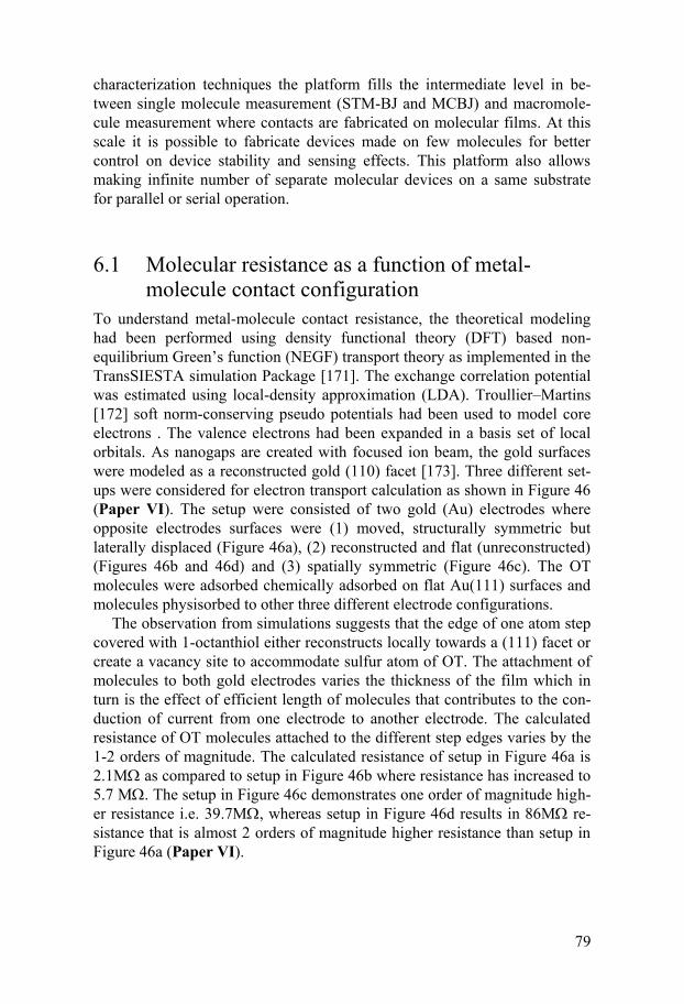
79
characterization techniques the platform fills the intermediate level in be-tween single molecule measurement (STM-BJ and MCBJ) and macromole-cule measurement where contacts are fabricated on molecular films. At this scale it is possible to fabricate devices made on few molecules for better control on device stability and sensing effects. This platform also allows making infinite number of separate molecular devices on a same substrate for parallel or serial operation.
6.1 Molecular resistance as a function of metal-molecule contact configuration
To understand metal-molecule contact resistance, the theoretical modeling had been performed using density functional theory (DFT) based non-equilibrium Green’s function (NEGF) transport theory as implemented in the TransSIESTA simulation Package [171]. The exchange correlation potential was estimated using local-density approximation (LDA). Troullier–Martins [172] soft norm-conserving pseudo potentials had been used to model core electrons . The valence electrons had been expanded in a basis set of local orbitals. As nanogaps are created with focused ion beam, the gold surfaces were modeled as a reconstructed gold (110) facet [173]. Three different set-ups were considered for electron transport calculation as shown in Figure 46 (Paper VI). The setup were consisted of two gold (Au) electrodes where opposite electrodes surfaces were (1) moved, structurally symmetric but laterally displaced (Figure 46a), (2) reconstructed and flat (unreconstructed) (Figures 46b and 46d) and (3) spatially symmetric (Figure 46c). The OT molecules were adsorbed chemically adsorbed on flat Au(111) surfaces and molecules physisorbed to other three different electrode configurations.
The observation from simulations suggests that the edge of one atom step covered with 1-octanthiol either reconstructs locally towards a (111) facet or create a vacancy site to accommodate sulfur atom of OT. The attachment of molecules to both gold electrodes varies the thickness of the film which in turn is the effect of efficient length of molecules that contributes to the con-duction of current from one electrode to another electrode. The calculated resistance of OT molecules attached to the different step edges varies by the 1-2 orders of magnitude. The calculated resistance of setup in Figure 46a is 2.1M as compared to setup in Figure 46b where resistance has increased to 5.7 M. The setup in Figure 46c demonstrates one order of magnitude high-er resistance i.e. 39.7M, whereas setup in Figure 46d results in 86M re-sistance that is almost 2 orders of magnitude higher resistance than setup in Figure 46a (Paper VI).

80
Figure 46. Atomic configurations considered in theoretical simulation – side view of the contact area seen along [-1 1 0] direction. Different structures obtained by mov-ing the top electrode correspond to different inter-electrode separations. a) Symmet-ric but laterally displaced (moved) electrodes b) reconstructed (flat) c) spatially symmetric surfaces d) one flat electrode with additional 2Å. (Adopted from Paper VI and reproduced with the permission of IOP)
6.2 Molecules in bridge platform by self-assembled monolayer formation on nanoelectrodes
Formation of self-assembled monolayer (SAM) of molecules on gold surfac-es has been carried out since 1960. SAM layers of very high quality have been achieved on perfect <111> or <100> gold surfaces. It is possible to achieve stable chemisorbed metal-molecule junctions when molecules are terminated by thiols (-SH), this is due to chemical affinity of thiols to gold atoms. Figure 47 shows metal-molecule junctions that were prepared by formation of self-assembled monolayer (SAM) on nanoelectrode surfaces.
Figure 47. Schematic representations of molecular electronic devices prepared by dielectrophoretic trapping of clean AuNP in between a) OT molecules b) BPDT molecules c) mixed OT and BPDT self-assembled monolayer coated gold nanoelec-trodes.
In a first batch, devices were prepared by placing clean nanoelectrodes in 0.1 M OT for 24 hours (Figure 47a, Paper VI). In a next batch, devices were functionalized by placing nanoelectrodes in 0.1mM BPDT solution in etha-nol for 48 hours under argon atmosphere (Figure 47b, Paper VI). The sur-faces of the nanoelectrodes contains a high number of step edges that should result in a defective SAM of the thiol terminated molecules, exploring this scenario the nanoelectrodes were covered with mixed SAM layer of OT and
a) b) c) d)
a) b) c)AuNPOT BPDT
Si/SiO2
Gold

81
BPDT (Figure 47c, Paper VIII). For preparation of mixed SAM layer of OT and BPDT, the clean nanoelectrodes were placed first in 0.1mM OT for 24 hours and subsequently placed in 0.1mM BPDT in argon atmosphere for 24 hours. In order to bridge the nano-gap in between SAM coated nanoelec-trodes 30nm AuNPs in aqueous solution (EM.GC30, BBInternational, Car-diff, UK) were trapped by dielectrophoretic forces using AC voltages.
6.2.1 Electrical characterization of devices containing 1-octanethiol molecules
In Figure 48a, the I-V characteristics of the device (SEM inset) containing OT molecules in between AuNP-nanoelectrode bridge platform is shown. The three consecutive I-V measurements on this setup have demonstrated the stability and reproducibility of the device property as shown in Paper VI. Normally AuNPs demonstrate coulomb blockade in such setup [174], but coulomb blockade cannot be observed due to size of AuNP (30nm) and measurements are carried out at room temperature.
Figure 48. a) I-V characteristics of OT in between AuNP-nanoelectrode bridge platform (inset: SEM of device, scale bar is 100nm) b) Resistance histogram of trapped AuNPs between OT coated nanoelectrodes. (Adopted from paper VI and Reproduced with the permission from IOP)
In the device shown in inset of Figure 48a, a single AuNP (30nm) bridges OT coated electrodes and the conduction occurs through two metal-molecule junctions in series. Considering a contact surface of 30nm AuNP with gold electrodes it is estimated that in this case each junction is consisted of about 10 molecules. Estimation has been done by considering that packing density of OT on gold surface is 4.6molecules/nm [175]. This device demonstrates the low bias resistance in order of 35G that translates into single OT mole-cule resistance in the order of ~175G (Paper VI), which is in good agree-ment with previous studies carried out on OT attached to gold surface[123]. In general, the low conductivity of OT is attributed to the 8eV HOMO-LUMO gap [176] and transport mechanism through alkane chains [123].
0
25
50
-25
-50
Voltage bias (V)
Cur
rent
(pA
)
0.4 0.8 1.20-0.4-0.8-1.2
CO
UN
T
Resistance ()102 104 106 108 1010 1012 1014
0
2
4
6

82
In OT based devices as shown in Figure 48a, current fluctuation has been observed with an applied voltages above ±0.5V that is attributed to either formation of the gauche defects [177] or mobility of the molecules chemi-sorbed to gold via a thiol link under high bias voltage [59, 178, 179]. Non-linearity is observed in the I-V curve at higher voltages up to 2V (Paper VI) [180]. As shown in section 3.5, nanoelectrodes with a gap size of 20-30nm are reproducible and can be fabricated in abundance. It is possible to fabri-cate a number of devices and observe reproducibility of particular metal-molecule junction in this setup. The resistance histogram of OT based devic-es in AuNP-nanoelectrode bridge platform is shown in Figure 48b, where the average resistances of devices were measured in linear region below applied bias voltages of 100mV. The resultant histogram has demonstrated a large variation in magnitude where most of devices have resistance between 100M to 10T. FIB milling during nanoelectrode fabrication on polycrys-talline gold lines produces uneven surfaces. Surface coverage of SAM on polycrystalline substrate is expected to be imperfect and “pinholes” are usu-ally present in SAMs on perfect gold surfaces [181]. Presence of pinholes in SAM layer leads to metal-metal contact, which is responsible for low re-sistance devices in histogram. However the majority of device resistances exist in between 1G to 10T. This large variation can be attributed to the number of trapped AuNPs, incomplete coverage of SAM layer on nanoelec-trode surfaces, contamination/impurity contributions and variation in contact surface geometry (Paper VI) as described in detail in section 6.1.
6.2.2 Electrical characterization of devices containing 4,4´-biphenyldithiol
4,4´-biphenyldithiol (BPDT) is supposed to be highly conductive due to the presence of π- conjugation of molecules that result in the delocalized elec-trons. However I-V characteristics of most devices in our platform either demonstrated a metallic behavior or open circuit response having resistances more than 100T. Yield of devices having SAM layer of BPDT as shown in Figure 47b is less than 5%, the low yield behavior of BPDT based devices is also reported in literature [182]. This could be related to either partial oxida-tion of BPDT or to “Backbiting”. Backbiting in the molecules refers to a geometric shape of thiol termination at the both ends of molecules, where both thiol ends of the molecule get attached to the same gold surface. The backbiting of dithiolated molecules is a major cause of failure in preparation of molecular devices with dithiolated molecules in the devices where the real intention is to connect opposite gold surfaces with chemisorbed metal-molecule junctions.
The I-V characteristics of BPDT in between AuNP-nanoelectrode bridge platform have demonstrated linearity at lower applied voltages with re-
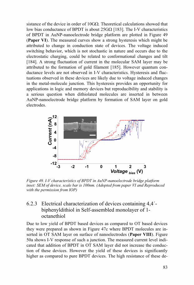
83
sistance of the device in order of 10G Theoretical calculations showed that low bias conductance of BPDT is about 25G [183]. The I-V characteristics of BPDT in AuNP-nanoelectrode bridge platform are plotted in Figure 49 (Paper VI). The measured curves show a strong hysteresis which might be attributed to change in conduction state of devices. The voltage induced switching behavior, which is not stochastic in nature and occurs due to the electrostatic charging, could be related to conformational changes and tilt [184]. A strong fluctuation of current in the molecular SAM layer may be attributed to the formation of gold filament [185]. However quantum con-ductance levels are not observed in I-V characteristics. Hysteresis and fluc-tuations observed in these devices are likely due to voltage induced changes in the metal-molecule junction. This hysteresis provides an opportunity for applications in logic and memory devices but reproducibility and stability is a serious question when dithiolated molecules are inserted in between AuNP-nanoelectrode bridge platform by formation of SAM layer on gold electrodes.
Figure 49. I-V characteristics of BPDT in AuNP-nanoelectrode bridge platform inset: SEM of device, scale bar is 100nm. (Adopted from paper VI and Reproduced with the permission from IOP)
6.2.3 Electrical characterization of devices containing 4,4´-biphenyldithiol in Self-assembled monolayer of 1-octanethiol
Due to low yield of BPDT based devices as compared to OT based devices they were prepared as shown in Figure 47c where BPDT molecules are in-serted in OT SAM layer on surface of nanoelectrodes (Paper VIII). Figure 50a shows I-V response of such a junction. The measured current level indi-cated that addition of BPDT in OT SAM layer did not increase the conduc-tion of these devices. However the yield of these devices is significantly higher as compared to pure BPDT devices. The high resistance of these de-
-1.2E-08
-8.0E-09
-4.0E-09
0.0E+00
4.0E-09
8.0E-09
1.2E-08
-3 -2 -1 0 1 2 3
0
4
12
-12
Voltage bias (V)
Cur
rent
(nA
)
1 2 30-1-2-3
-8
-4
8

84
vices may be attributed to formation of disulfide bonds or backbiting of BPDT molecules [186]. The non-linearity in I-V curves is again due to non-resonant coherent tunneling as measured in several studies previously [123]. The measured resistance of all such devices at voltages lower than 100mV is plotted in log-linear histogram (Figure 50b). Due to large distribution of data, geometric mean resistance of these devices is calculated. The geomet-ric mean resistance of devices with mixed SAM layer of OT and BPDT is approximately 127G (Paper VIII). It can be seen that the introduction of BPDT molecule in between SAM layer of OT reduces the variation in re-sistance (spread in histogram) as compared to SAM layer OT (Figure 48b). None of the devices exhibited a metallic behavior, which indicated that dur-ing the BPDT functionalization step the BPDT molecules filled pinholes in OT SAM layer.
Figure 50. a) I-V characteristics of OT and BPDT in between AuNP-nanoelectrode junction b) log normal resistance histogram of devices. (adopted from paper VIII and reproduced with the permission from Elsevier)
6.3 Monothiolated molecules in bridge platform by coating of molecules on gold nanoparticles surfaces
In order to get reproducible electrical characteristics of the metal-molecule junction and the AuNP-nanoelectrode bridge platforms, the surfaces of AuNPs were stabilized by 1-alkanethiols. AuNPs were prepared by reduc-tion of gold salt in presence of 1-dodecanethiol (DT) in a one-pot process [187]. The size of DT coated AuNPs varied between 5-10nm. The size of AuNPs was relatively small as compared to 15-25 nm gap size. In order to bridge a nanogap in between nanoelectrodes, at least 10-15 DT coated AuNPs were required and hence number of trapped AuNPs became irrele-vant as compared to 30nm AuNP trapped in between nanoelectrodes. Two different metal-molecule junctions were fabricated. Device I was prepared by dielectrophoretic trapping of DT coated AuNPs in between clean nanoe-
0 1
60
40
20
0
-40
-20
2-1-2
Cur
rent
(pA)
Voltage (V)
a)
0
5
10
10 11 12 13 14Log 10[Resistance ()]
CO
UN
TSb)
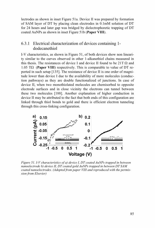
85
lectrodes as shown in inset Figure 51a. Device II was prepared by formation of SAM layer of DT by placing clean electrodes in 0.1mM solution of DT for 24 hours and later gap was bridged by dielectrophoretic trapping of DT coated AuNPs as shown in inset Figure 51b (Paper VIII).
6.3.1 Electrical characterization of devices containing 1-dodecanethiol
I-V characteristics, as shown in Figure 51, of both devices show non lineari-ty similar to the curves observed in other 1-alkanethiol chains measured in this thesis. The resistances of device I and device II found to be 21T and 1.05 T (Paper VIII) respectively. This is comparable to value of DT re-ported in such setup [135]. The resistance of device II is one order of magni-tude lower than device I due to the availability of more molecules (conduc-tion pathways) as they are double functionalized of junctions. In case of device II, when two monothiolated molecules are chemisorbed to opposite electrode surfaces and in close vicinity the electrons can tunnel between these two molecules [188]. Another explanation of higher conduction in device II may be attributed to the fact that both ends of this configuration are linked through thiol bonds to gold and there is efficient electron tunneling through this cross-linking configuration.
Figure 51. I-V characteristics of a) device I, DT coated AuNPs trapped in between nanoelectrode b) device II, DT coated gold AuNPs trapped in between DT SAM coated nanoelectrodes. (Adopted from paper VIII and reproduced with the permis-sion from Elsevier)
Cur
rent
(pA
)
Voltage (V)
a) b)

86
6.4 Dithiolated molecules in bridge platform by coating of -thiol protected molecules on gold nanoparticles surfaces
A large distribution in resistance histograms of OT and DT in between nano-electrodes and AuNPs may be attributed to physisorbed junction at one end of molecules. It is also found that attempts to prepare chemisorbed junctions between two gold surfaces by SAM layer of dithiolated molecule (BPDT) could not yield enough devices due to formation of incomplete SAM cover-age, backbiting and disulfide bonding of neighbor molecules. Coating of AuNPs with dithiolated molecules, where one end remains unbound is of particular interest in the field of molecular electronics, as it provides oppor-tunity for chemisorbed junction to the gold surface or to macromolecule. It is still considered as a technological challenge. Monomeric gold AuNPs coated with dithiols molecules were prepared (Paper IX) by wet chemistry. Gold AuNPs coated with -trityl protected alkanedithiol were synthesized as shown in Figure 52, where the outer end of thiol group at monolayer surface can be deprotected with the removal of protective trityl groups under mild insitu conditions i.e. treating the sample with mixture of 5 mL trifluoroacetic acid, 5 mL dichloromethane and 0.5 mL triethylsilane, which results in free thiol groups at the outer end of the alkanedithiols available for formation of chemisorbed junctions with nearby gold surface (Paper V, IX, X and XI).
Figure 52. a,b) Synthesis of mixed self-assembled monolayer of stabilized AuNPs with thiol terminated alkane chains a) reaction scheme of protected thiol ends of alkanedithiol with trityl chloride b) reaction scheme of AuNP preparation by reduc-tion of HAuCl4 c) TEM image of AuNPs with average size of 4.9±1.1nm. (Adopted from paper IX and reproduced with the permission of ACS)
Details of the synthesis of the -trityl protected ODT coated AuNPs are described in detail in Paper IX and scheme is shown in Figure 52a and 52b. In brief, a solution of 1.90 mmol HAuCl4×3H2O and 1.90 mmol of the corre-sponding α,ω-bis(triphenylmethylthio)alkane in 20 ml of THF was vigorous-ly stirred at 25 °C until the solution started to become cloudy. To the result-
c)
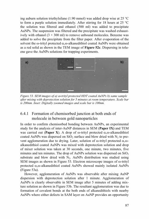
87
ing auburn solution triethylsilane (1.90 mmol) was added drop wise at 25 °C to form a purple solution immediately. After stirring for 18 hours at 25 °C the solution was filtered and ethanol (500 ml) was added to precipitate AuNPs. The suspension was filtered and the precipitate was washed exhaust-ively with ethanol (3 × 300 ml) to remove unbound molecules. Benzene was added to solve the precipitate from the filter paper. After evaporation of the solvent the -trityl protected -alkanedithiol coated AuNPs were obtained as a red solid as shown in the TEM image of Figure 52c. Dispersing in tolu-ene gave the AuNPs solutions for trapping experiments.
Figure 53. SEM images of a) -trityl protected HDT coated AuNPs b) same sample after mixing with deprotection solution for 5 minutes at room temperature. Scale bar is 200nm. Inset: Digitally zoomed images and scale bar is 100nm.
6.4.1 Formation of chemisorbed junction at both ends of molecule in between gold nanoparticles
In order to confirm chemisorbed bonding between AuNPs, an experimental study for the analysis of inter-AuNP distances in SEM (Paper IX) and TEM was carried out (Paper X). A drop of -trityl protected -alkanedithiol coated AuNPs was dispersed on SiO2 surface and blow dried with N2 to pre-vent agglomeration due to drying. Later, solution of -trityl protected -alkanedithiol coated AuNPs was mixed with deprotection solution and drop of mixer solution was taken at 30 seconds, one minute, two minutes, five minutes and ten minutes. The drop of AuNPs solution was dispersed on SiO2 substrate and blow dried with N2. AuNPs distribution was studied using SEM images as shown in Figure 53. Electron microscope images of -trityl protected -alkanedithiol coated AuNPs showed mainly isolated AuNPs (Figure 53a).
However, agglomeration of AuNPs was observable after mixing AuNP dispersion with deprotection solution after 1 minute. Agglomeration of AuNPs is clearly observable in SEM image after 5 minutes of adding mix-ture solution as shown in Figure 53b. The resultant agglomeration was due to formation of covalent bonds at the both ends of alkanedithiols with nearby AuNPs where either defects in SAM layer on AuNP provides an opportunity
a) b)

88
for the deprotected thiol groups to attach or exchange reactions [189] of free thiol groups with the surface bonded sulfur atom from nearby AuNPs. In addition to this experiment NMR studies confirmed that trityl protective groups have been efficiently removed by addition of deprotection agent.
Figure 54. TEM images of a) -trityl protected ODT molecules coated AuNPs, b) after removal of trityl protective groups from end of ODT molecules coated AuNPs in dispersion. Scale bar: 20nm
Samples were also prepared on TEM holey carbon grids again following the same protocol as described before. Transmission electron microscopy has been carried out using FEI Tecnai F30 ST at 300kV. TEM observations of the -trityl protected ODT molecules coated AuNPs have revealed that it is difficult to find any agglomeration of AuNPs as these are mono-dispersed as shown in Figure 54a. However, few AuNPs are in vicinity of each other and inter-AuNPs distances vary between 1.4 nm to 5nm with an average distance of 2.8nm. TEM image of AuNPs after removal of trityl protective groups from -end of ODT molecules is shown in Figure 54b reveals chains of AuNPs. The removal of the trityl protective group leads to formation of chemisorbed metal molecule junction at the both ends of ODT molecules between AuNPs. The distance between two adjacent AuNPs varies in be-tween 5.9Å to 14Å with an average distance of 1nm.
6.4.2 Formation of chemisorbed junction at both ends of molecule in gold nanoparticle-nanoelectrode bridge platform
Dielectrophoretic trapping of the -trityl protected -alkanedithiol coated AuNPs was carried out on clean nanoelectrodes. I-V characterization of trapped AuNPs with protective group on end of molecules in between nanoe-lectrode was carried out consecutively. In order to achieve chemisorbed junction at the both ends of molecules in between AuNP-nanoelectrode bridge platform, the sample was placed in mixture solution of 5 mL tri-
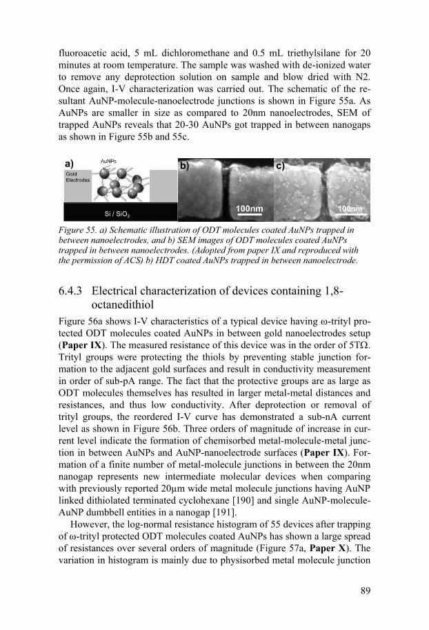
89
fluoroacetic acid, 5 mL dichloromethane and 0.5 mL triethylsilane for 20 minutes at room temperature. The sample was washed with de-ionized water to remove any deprotection solution on sample and blow dried with N2. Once again, I-V characterization was carried out. The schematic of the re-sultant AuNP-molecule-nanoelectrode junctions is shown in Figure 55a. As AuNPs are smaller in size as compared to 20nm nanoelectrodes, SEM of trapped AuNPs reveals that 20-30 AuNPs got trapped in between nanogaps as shown in Figure 55b and 55c.
Figure 55. a) Schematic illustration of ODT molecules coated AuNPs trapped in between nanoelectrodes, and b) SEM images of ODT molecules coated AuNPs trapped in between nanoelectrodes. (Adopted from paper IX and reproduced with the permission of ACS) b) HDT coated AuNPs trapped in between nanoelectrode.
6.4.3 Electrical characterization of devices containing 1,8-octanedithiol
Figure 56a shows I-V characteristics of a typical device having -trityl pro-tected ODT molecules coated AuNPs in between gold nanoelectrodes setup (Paper IX). The measured resistance of this device was in the order of 5T. Trityl groups were protecting the thiols by preventing stable junction for-mation to the adjacent gold surfaces and result in conductivity measurement in order of sub-pA range. The fact that the protective groups are as large as ODT molecules themselves has resulted in larger metal-metal distances and resistances, and thus low conductivity. After deprotection or removal of trityl groups, the reordered I-V curve has demonstrated a sub-nA current level as shown in Figure 56b. Three orders of magnitude of increase in cur-rent level indicate the formation of chemisorbed metal-molecule-metal junc-tion in between AuNPs and AuNP-nanoelectrode surfaces (Paper IX). For-mation of a finite number of metal-molecule junctions in between the 20nm nanogap represents new intermediate molecular devices when comparing with previously reported 20µm wide metal molecule junctions having AuNP linked dithiolated terminated cyclohexane [190] and single AuNP-molecule-AuNP dumbbell entities in a nanogap [191].
However, the log-normal resistance histogram of 55 devices after trapping of -trityl protected ODT molecules coated AuNPs has shown a large spread of resistances over several orders of magnitude (Figure 57a, Paper X). The variation in histogram is mainly due to physisorbed metal molecule junction
100nm
a) b) c)
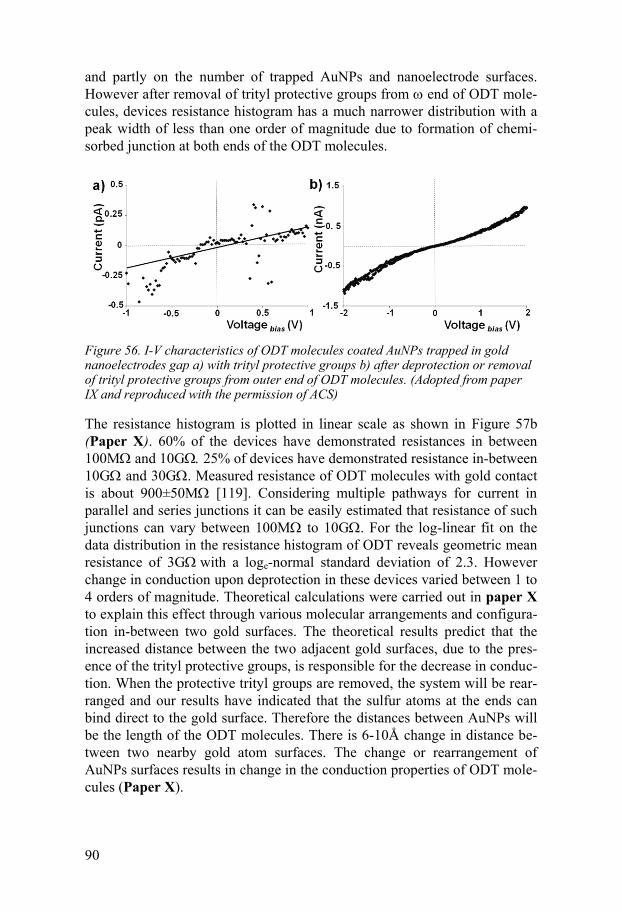
90
and partly on the number of trapped AuNPs and nanoelectrode surfaces. However after removal of trityl protective groups from end of ODT mole-cules, devices resistance histogram has a much narrower distribution with a peak width of less than one order of magnitude due to formation of chemi-sorbed junction at both ends of the ODT molecules.
Figure 56. I-V characteristics of ODT molecules coated AuNPs trapped in gold nanoelectrodes gap a) with trityl protective groups b) after deprotection or removal of trityl protective groups from outer end of ODT molecules. (Adopted from paper IX and reproduced with the permission of ACS)
The resistance histogram is plotted in linear scale as shown in Figure 57b (Paper X). 60% of the devices have demonstrated resistances in between 100M and 10G 25% of devices have demonstrated resistance in-between 10G and 30G. Measured resistance of ODT molecules with gold contact is about 900±50M [119]. Considering multiple pathways for current in parallel and series junctions it can be easily estimated that resistance of such junctions can vary between 100M to 10G. For the log-linear fit on the data distribution in the resistance histogram of ODT reveals geometric mean resistance of 3Gwith a loge-normal standard deviation of 2.3. However change in conduction upon deprotection in these devices varied between 1 to 4 orders of magnitude. Theoretical calculations were carried out in paper X to explain this effect through various molecular arrangements and configura-tion in-between two gold surfaces. The theoretical results predict that the increased distance between the two adjacent gold surfaces, due to the pres-ence of the trityl protective groups, is responsible for the decrease in conduc-tion. When the protective trityl groups are removed, the system will be rear-ranged and our results have indicated that the sulfur atoms at the ends can bind direct to the gold surface. Therefore the distances between AuNPs will be the length of the ODT molecules. There is 6-10Å change in distance be-tween two nearby gold atom surfaces. The change or rearrangement of AuNPs surfaces results in change in the conduction properties of ODT mole-cules (Paper X).

91
Figure 57. a) Log-normal histogram of -trityl protected ODT molecules coated AuNPs in between nanoelectrodes. b) Resistance Histogram of ODT molecules coated AuNPs after removal of trityl protective group and formation of chemisorbed junction at the both end of ODT molecule, shaded bar indicates the devices with resistances less than 100M. (Adopted from paper X)
6.4.4 Electrical characterization of devices containing 1,6-hexanedithiol
-Trityl protected HDT coated AuNPs were also trapped in 20nm gold nanogap in between nanoelectrodes. Typical I-V characteristics of protected molecules (dot line), as shown in Figure 58a, have shown a nonlinear re-sponse and current levels in sub-nA range (Paper X).
Figure 58. a) I-V characteristics of HDT in AuNP-nanoelectrode bridge platform, (1) before and (2) after removal of -trityl protective groups from outer end of mol-ecules. b) Resistance histogram of HDT in AuNP-nanoelectrode bridge platform with bin size of 200MAdopted from paper X
The low bias resistance of this device with -trityl protected HDT molecules in between AuNP-nanoelectrode bridge platform is 5G. The same device after deprotection has demonstrated a 25 times higher current level than the protected device (Figure 58a solid line). The recorded I-V curves are non-linear and demonstrate a low bias resistance of 179M. The resistance his-togram of 26 devices (Paper X) of HDT molecules in AuNP-nanoelectrodes bridge platform after removal of protective groups is shown in Figure 58b. 60 % of devices show resistance value in range of 100M to 600M. Ge-

92
ometric mean resistance of all devices is found to 510M. The measured resistance of HDT almost demonstrated the same value in AuNP-nanoelectrode bridge platform as reported in literature [135].
6.5 Shelf-life of molecular devices in air, water and organic solvents
One of the major concerns for the application of molecular electronic devic-es is the stability and the durability of molecular device over the period of time. Molecular electronic devices are prepared by dielectrophoretic trapping of ODT molecules coated AuNPs in between gold nanoelectrodes and later these devices were stored over a period of one month in ambient condition, water, tetrahydrofuran (THF), toluene and tetramethylethylenediamine (TMEDA) (Paper V). Figure 59a shows the I-V characteristics of a typical molecular (ODT molecules) device that was stored over the period of 28 days in ambient conditions without changing its properties significantly. Device resistance changed from 2.98G (week 0) to 1.78G (week 1) to 2.54G (week 4). However, the half of the devices stopped conducting or demonstrated very low conductance in Tregime after 4 weeks. Molecular electronic devices have been stored in de-ionized water (polar inorganic solvent), toluene (non-polar, organic solvent), THF (polar organic solvent) and TMEDA (ligand for metal ion). Molecular devices have demonstrated a change in resistance every week, when stored in water, THF and Toluene (Paper V). However devices stored in TMEDA, minute change in the re-sistance was observed during the period of 28 days as shown in Figure 59b. It might be related to the formation of bonds between the ligand molecules (TMEDA) and gold atoms on the nanoelectrodes surfaces. When these de-vices are stored in water and the organic solvent, all the devices except one have survived over the period of 4 weeks.
6.6 Inelastic electron tunneling spectroscopy of 1,8-octanedithiol molecules in nanoparticle-nanoelectrode bridge platform
The nanoelectrodes platform was attached and wire bonded to chip holder as discussed in Chapter 3.5. After cutting gaps, dielectrophoretic trapping of -trityl protected ODT molecules coated AuNPs was carried out in between gold nanoelectrodes. The outer protective groups were later removed by immersing the platform in deprotection solution to establish chemisorbed junction at the both ends of ODT molecules in AuNP-nanoelectrode bridge platform.

93
Figure 59. I-V characteristics of ODT molecules based electronic device a) stored in ambient condition b) stored in TMEDA for 28 days. Adopted from paper V
Figure 60. a) I-V characteristics of ODT molecules trapped in between AuNP-nanoelectrode bridge platform measured at 4K. b) Measured abs (dI/dV) vs. V of the same device measured. (Adopted from paper XI)
Figure 61. IETS spectra of ODT molecules in between AuNP-nanoelectrode bridge platform a)two experimentally measured curve taking at amplitude of AC voltage of 30mV b) Calculated IETS using the modeling described fitting(least square) the number of chains with N= 4,5…,14. (Adopted from paper XI)
In order to observe molecular vibrations of ODT molecules in AuNP-nanoelectrode platform, the samples were inserted in the chip holder of the dipstick. The dipstick was inserted in the cylinder filled with liquid helium and the I-V characterization along with IETS measurements were carried out at 4.2K (Paper XI). In the I-V characteristics, a clear Coulomb blockade was observed at 4.2K due to the 5nm size of AuNPs as shown in Figure 60a.
----Week 0----Week1----Week3----Week4
Voltage bias (V)
Cur
rent
(nA) 0
0.5
1
-0.5
-1
Cur
rent
(nA
)
Voltage bias (V)
0.5
1.5
2.5
-0.5
-1.0Cur
rent
(nA
)
a) b)
----Week 0----Week1----Week3----Week4
0 0.5 1-0.5-1 0 0.5 1-0.5-1-1.5
0 1 2-1-2
0
-1
-2
1
2
Voltage bias (V)
Cur
rent
(nA
)
0 1 2-1-20.5x10⁻⁹
1.0x10⁻⁹
1.5x10⁻⁹
2.0x10⁻⁹
Voltage bias (V)
AB
S dI
/dV(
A/V
)a) b)
0 1 2-1-20
2
4
6
8
10
Voltage (V)
│Im
d2I/d
V2│
(nA/
V2) a) b)

94
Asymmetry was observed in IV response, resulting from the devices itself. It might have arisen due to asymmetric surfaces of nanoelectrodes or due to the number of active junctions in positive and negative voltage sweep [192]. Two lock-in amplifiers (Stanford research systems Model SR830 DSP) were used to collect 1st and 2nd harmonics from small AC signal imposed on sweeping DC bias. In Figure 60b, the first derivative (dI/dV vs. applied volt-age) is plotted. The first derivate indicates the availability of density of states at the applied voltage for electron transport. Furthermore, in dI/dV during negative biasing the signal decreased at several points. Such incidences could be related to the events where molecular vibrations transmit their en-ergy to the tunneling electrons.
The Inelastic electron tunneling spectroscopy (IETS) signal is strongest in the imaginary part of the measured 2nd harmonics of the signal. In Figure 61, we have plotted measured and calculated IETS spectra of a typical de-vice. Figure 61a shows experimentally measured two IETS spectra of ODT molecules in between AuNP-nanoelectrode bridge platform with the energy resolution of 30mV. The presence of peaks in the signal indicates conduction through molecular states available in between metal-molecule junctions in this bridge platform. The peaks in figure 61a are asymmetric for negative and positive biasing due to different molecular configurations in different chains of AuNP-molecule junctions [192]. Nevertheless, peaks at low bias voltages appear at similar energies for negative and positive bias. To under-stand the nature of peaks from measured signal, theoretical calculations have been carried out (Paper XI). To simulate the case of multiple parallel junc-tions with molecules, the numbers of junctions were estimated by consider-ing the first peak of IETS signal as a combination Coulomb blockade peak of the whole device (Paper XI). In theoretical model, following vibrational mode at 40meV (Au-S), 84meV (ν(C-S)G), 109meV (CH2 Rocking), 122meV (C-C stretch) and 140meV (νa(C-S)T) are considered. The theoreti-cal calculated curves are calculated at Ec=25meV and overlaid on the exper-imental observation as shown in Figure 61b. The temperature was adjusted at T=20K and the experimental curve shown in Figure 61b has been Lo-rentzian broadened by 10meV. The calculated curve matches with experi-mental value when AuNPs-molecules network from one electrode to another electrode consists of parallel chains of 4, 5…, 14 molecules. It is possible to assign the first two peaks in IETS spectra to molecular vibrations as meas-ured peaks at higher applied bias will be a complex combination of ODT chains. For example, the first peak at 250mV has FWHM of 80mV and from its energy position it can be estimated that it contains Au-S molecular vibra-tions from AuNP-molecule chains of 5, 6 and 7 molecule junctions (Paper XI).
Hence it is possible to observe molecular vibrations in AuNP-nanoelectrode bridge platform. The model consists of chains of AuNP-molecule junctions where each chain connects the two nanoelectrodes with a

95
number of junctions in the chain. From IETS spectra it is possible to esti-mate the number of parallel AuNP-molecule chains taking part in conduction of electrons in 2D or 3D configuration of AuNP-molecule chains. (Paper XI).
Chapter Conclusions Molecules (1-dimentional nano-object) can be considered as one dimension-al wire. To obtain a reliable and reproducible system, molecules are intro-duced in between AuNP-nanoelectrode bridge platform either by self assem-bled monolayer molecular coating of nanoelectrode surfaces or by stabilizing AuNPs with molecules using the chemical affinity between thiol (-SH) and gold atoms. Coating of gold nanoelectrodes with OT where nanogap was bridged by trapped AuNPs have resulted several order of magnitude varia-tions in resistance of these devices due to physisorption of one end of the OT molecules to the trapped AuNPs. Coating of nanoelectrodes with BPDT molecules that could attach to both AuNPs and nanoelectrodes though chem-isorption, have resulted in a very low yield due to the backbiting of the dithi-olated molecules, formation of the disulfide bonds and oxidation of thiol bonds.
To insert molecules that can connect to AuNPs as well as nanoelectrodes through chemisorbed -SH bonds, a new functionalized technique was adopt-ed. This technique relies on the coating of AuNPs with dithiolated molecules where one thiolated end of the molecule was chemisorbed on the AuNP sur-face, whereas the other thiolated end of the molecule was protected with a trityl group to prevent it from the oxidation or backbiting. These AuNPs were trapped in between the clean nanoelectrodes and protective groups were removed which had resulted immediately in the formation of the chem-isorbed junction at both ends of the molecules with nearby gold surface of AuNPs or nanoelectrode.
These devices have demonstrated high reproducibility in the electronic and the electrical properties. It was found that the electrical properties of such devices can be stable over a period of month if stored in tetrameth-ylethylenediamine (TMEDA). These devices clearly indicate presence of molecular vibrations during inelastic electron tunnel spectroscopy measure-ments. Thus, this system provides a stable testbed for the molecular charac-terization at the room temperature as well at very low temperatures.

96
7 Concluding remarks
Graphene, molecules and nanoparticles will be important building blocks of novel materials used for future electronic, optical and mechanical devices with applications in processors, memories and sensors. These materials pro-vide exciting and exotic properties due to their low dimensional structure.
In this thesis, it has been demonstrated that conduction properties of gra-phene can be modified by creation of defects. The chemical treatment of free standing graphene sheets creates di-vacancy defects in graphene lattice. Di-vacancy defects give rise to mid-gap states, which lead to an increase in conductivity of the graphene sheet by at least one order of magnitude. In contrast, creation of defects by irradiation of gallium ions on exfoliated gra-phene sheet decreases the conductivity. The decrease in conductivity is at-tributed to creation of scattering centers in graphene lattices, rearrangement of atoms into amorphous carbon and debris from sputtering of silicon oxide substrate. The graphene conductivity was reduced by 20% with gallium ion dose radiation of 0.18 ions/nm2.
Nanoparticle-nanoelectrode bridge platform was successfully employed to characterize nanoparticles and molecules. Surfaces of nanoelectrodes and nanoparticles were prepared carefully following proper cleaning protocol to prepare a stable metallic junction between AuNP and nanoelectrode. Trap-ping of AuNPs in nanoelectrodes has resulted in highly conductive junction. A highly conductive junction is necessary for application of AuNP-nanoelectrode bridge platform in characterizing molecules as otherwise the molecular properties will be overshadowed by junction properties. The high resistance nanogaps provide a test bed to measure physical properties of semiconductor nanoparticles. The 20nm cadmium telluride tetrapods coated with oleic acid has demonstrated photoconductive response when trapped in between nanoelectrodes. The nanoparticles-nanoelectrode bridge platform is a stable platform that can be used to characterize and study physical proper-ties of metallic and semiconductor nanoparticles.
Molecules were introduced in between AuNPs-nanoelectrodes bridge platform by formation of self-assembled monolayer on nanoelectrode sur-faces. A self assembled monolayer of 1-alkanethiol results in large variation in device resistance due to physisorbed junction at one end of the molecules. In contrast self-assembled monolayer of dithiolated molecules on nanoelec-trodes resulted in low yield. The scheme that relies on protection and depro-tection chemistry has resulted in chemisorbed junction at both ends of the
97
dithiolated molecule. It is possible to prepare molecular devices with repro-ducible electronics properties. Molecular vibrations of molecules from IETS signal in AuNP-nanoelectrode junction has been observed and from the theo-retical modeling the numbers of parallel AuNP-molecule chains has been estimated. These devices are stable over a period of one month when stored in tetramethylethylenediamine (TMEDA). Hence it is demonstrated that the AuNP-nanoelectrode bridge platform is a stable setup that can be used to characterize few molecules as well as for fabrication of novel devices based on AuNPs and molecules.
7.1 Outlook Exciting and exotic electronic properties of low dimensional nano-objects is a solution for ultra-fast computing, highly-dense memory, nano-sized sen-sors and highly efficient energy generators.
Modification in the conduction properties in graphene and graphene like material make them perfect candidate for electronic devices and sensors. In commercial use of graphene, it will be required to modify the conduction properties of a graphene sheet at certain areas to control the electron flow across it. Such modification in conduction properties of graphene can be done not only by defects but also by ad-atoms and adsorption of gases. The next crucial step is to open the band gap in graphene sheets. Though it has been demonstrated that bilayer graphene sheet has some bandgap, however more experimental work is required to modify band gap of graphene. This work will continue in future in the field of gas sensing, molecule and poly-mer adsorption in defect induced graphene sheets.
Heightened activity of the surface atoms in nanoparticles make them per-fect candidates for use in single electron transistors, sensors and energy ap-plication. Using nanoelectrode platform it is possible to study the physical properties of single nanoparticles. This work will continue on measurements of electrical properties, gas sensing and photoconductivity in single and mul-tiple nanoparticles arrangements and in nano-rods of zinc oxide, zinc sulfide and cadmium sulfide.
Molecules provide unlimited variation in properties as they can be syn-thesized in any shape and size. The molecules in between AuNP-nanoelectrode platform have demonstrated a stable and reproducible plat-form for electrical characterization of molecules and molecular devices. Measurement was carried out on standard molecules such as 1-alkanethiols and ,-alkanedithiols. The next step will be to introduce other molecules in this platform such as tour compounds to measure their electronic properties and fabricate device with diode like behavior or light induced switching. This platform needs to demonstrate the possibility of gated measurement on molecules, which can be achieved either by the fabrication of side gates or

98
reducing the thickness of the underneath silicon dioxide to 50-70nm. Molec-ular devices based on this platform can be used as gas sensors or pH sensors by introduction of chemically reactive molecules either by coating of the nanoparticles or by place exchange process. The nanometric sizes of such devices enable us to carry out sensing inside biological cells or bacteria etc. In short, future electronic devices and sensors will be based on a single mol-ecule, nanoparticle and monolayer graphene sheet.
99
Summary in Swedish
Under de senaste 25 åren har den globala efterfrågan på supersnabb, billig och smart elektronik ökat exponentiellt. Industrin för integrerade kretsar har lyckats möta denna efterfrågan framgångsrikt med att göra snabbare och billigare apparater genom att minska storleken på transistorn från 10μm (1971) till 32nm (2010-11) i produktionen, och därmed packa fler transisto-rer per ytenhet. Men fysiska gränser sätter nu barriärer hur mycket snabbare, effektivare och billigare man kan göra dagens komponenter med hjälp av kiselbaserad teknik. Istället tittar man nu på flera nya nanomaterial som har potential att ersätta kisel. Experimentella och teoretiska arbeten om nanopar-tiklar, kolnanorör, molekyler samt grafen har visat att de har potential att flytta den fysikaliska barriären än en gång för snabbare och billigare elektro-niska komponenter, men fortfarande krävs mycket förståelse kring fysiken som styr dessa enheter för att i längden ha möjlighet att tillverka kommersi-ella apparater från dessa nanomaterial. Det är inte bara viktigt att undersöka egenskaperna hos enskilda nano-enheter utan också att utveckla en förståelse för av hur man sammankopplar dem. I denna avhandling har de fysiska egenskaperna, särskilt elektrisk analys av nanomaterial, skett genom att bygga en station som elektronisk kan undersöka enstaka nano-enheter.
Grafen är ett tvådimensionellt lager endast en atom tjockt av kolatomer i ett hexagonalt mönster. Grafen saknar bandgap, elektronernas mobilitet i materialet har slagit nya rekord och det har även visat förändringar i led-ningsförmåga när ett elektriskt fält läggs på. För att kunna använda grafen som grund för nästa generations elektroniska apparater måste dess lednings-förmåga finputsats. Här har ledningsförmågan av grafen ändrats genom att skapa defekter i strukturen, antingen genom kemisk behandling, dvs expone-ring mot mycket koncentrerad saltsyra tillsammans med förhöjd temperatur eller genom fysikaliska processer, vilket innebär bombardemang med 30 keV gallium joner. Kemisk behandling av fristående grafenlager skapar di-vakans defekter i strukturen, dessa medför att det blidas tillstånd inom bandgapet vilket i sin tur ökar ledningsförmågan av grafenarken åtminstone en storleksordning. En på plats (in situ) installation i fokuserade jon-stråle/svepelektron -mikroskopet (FIB/SEM) har byggts för att kunna analy-sera de fristående grafenarken med en 30-50nm stor vass spets utan att be-höva renrumsbearbetningstekniker. I motsats har defekter skapade med hjälp av bestrålning av gallium joner minskat ledningsförmågan av exfolierade grafenark. Minskningen av ledningsförmågan tillskrivs skapandet av sprid-
100
ningscentran i grafenstrukturen, omplacering av atomerna till amorft kol och fragment från det underliggande kiseldioxid substratet. Grafens lednings-förmåga minskade med 20% när galliumjon dosen var 0.18joner/nm2. Dessa experiment utfördes vid väldigt låga temperaturer för att se hur defekter skapas vid dessa. För att mäta dessa saker byggdes en uppställning in situ i FIB/SEM som mätte utan fördröjning.
Ökad aktivitet av ytatomer i nanopartiklar (0-dimensionella nano-objekt) gör dem till perfekta kandidater för användning i transistorer, sensorer och energitillämpningar. Förhållandet mellan yta och volym ger en ökad kemisk reaktivitet på grund av en förändrad aktivitet av hål och elektroner. På grund av kvantum instängning delas ledningsbandet i metalliska nanopartiklar (guld , silver etc.) delas upp i diskreta nivåer till skillnad från i bulk där det kontinuerligt. I nanopartiklar av halvledare finns förutom de diskreta nivåer-na i ledningsbandet ett stort bandgap, däremot när man dopar halvledar-nanopartiklar egenskaperna ändras och ändrar elektro- och katod-luminescensen. Att göra kontakter till nanopartiklar i en fast plattform som senare kan fungera som en apparat är en stor teknologisk utmaning som här löstes genom att fånga en nanopartikel mellan två elektroder med hjälp av en kraft som skapas på dielektriska partiklar med hjälp av icke-uniforma elekt-riska fält. Under de första mätningarna dominerade egenskaper från nanopar-tikel-nanoelektrod kopplingen och döljde de elektriska egenskaperna av själva nanopartikeln. För att få en metallisk kontakt mellan nanoelektroder och nanopartiklar av guld gjordes en förberedning och behandling av ytorna, det här ledde till en koppling med låg resistans vilket gör den här plattformen med metalliska nano-partiklar och -elektroder en ideal uppställning för ka-rakterisering av molekyler. För att testa fysikaliska egenskaperna av halvle-dar-nanopartiklar skapades även en tillförlitlig koppling mellan dessa och guld nano-elektroder. Här kunde fotokonduktiviteten observeras för 20nm kadmium-tellur tetrapods fångade i elektrodgapet.
Molekyler (1-dimensionella nano-objekt) kan i jämförelse med nanopar-tiklar betraktas som nano-trådar. Molekyler är väldigt intressanta eftersom de i stort sett tillåter obegränsat med variation of elektriska egenskaper ef-tersom de kan syntetiseras i en rik variation av storlek och form. Ett av de stora problemen för att integrera molekyler i elektroniska kretsar är att kunna koppla in sig på en eller några enstaka molekyler på och fortfarande ha ett reproducibelt och tillförlitligt system. För att göra stabila och reproducerbara kontakter till molekyler i nanoelektrod-nanopartikel plattformen här, kan deras egenskaper att skapa välorganiserade strukturer på ytor användas, an-tingen genom att belägga ytorna på nanoelektroderna eller genom att de sit-ter på ytan på en nanopartikel och stabiliserar den genom den kemiska drag-ningen mellan tioler (SH) och guldatomer. Mätningar på en beläggning av 1-alkantioler på guld elektroder, där elektrodgapet överbryggats med fångade guld nanopartiklar och ena änden på molekylen endast har en fysikalisk bindning till guld nanopartikeln, har visat på mer än 8 storleksordningar i

101
skillnad på uppmätt resistans hos olika enheter. Försök med beläggning av nanoelektroderna med molekyler som har tioler i båda ändarna som skulle kunna binda kemiskt till både elektrod och nanopartikel har resulterat i väl-digt lågt utbyte eftersom de istället antingen binder med båda tiolerna till nanoelektroden, skapar tiol-tiol bindningar eller att tiolgruppen oxideras.
Genom att föra in molekyler som kan kopplas till nanopartiklar samt nanoelektroder genom kemisorption av tiolgrupper så har en ny funktional-iseringsteknik utvecklats. Tekniker bygger på nanopartiklar som är täckta med ditiolmolekyler där ena tiolgruppen är kemisorberad på nanopartikely-tan och den andra (fria) tiolgruppen är skyddad av en tritylgrupp i syfte att undvika oxidation eller bindning tillbaka till nanopartikelytan. Nanopartik-larna har fångats in mellan rena nanoelektroder och därefter har tritylgrup-perna tagits bort vilket har resulterat i direkt formation av kemisorberade molekyler på nanopartiklarna eller nanoelektroderna. Dessa formationer av molekyler och nanopartiklar har uppvisat mycket reproducerbara elektriska egenskaper samt molekylära vibrationer genom inelastisk elektrontunnel-spektroskopi. Det har visat sig att dessa molekyl-nanopartikel-system är stabila om de förvaras i tetrametyletyldiamin (TMEDA) jämfört med om de förvaras i toluen där de är stabila under en månad.
Sammanfattningsvis har studierna i denna avhandling demonstrerat olika system som kan användas för att undersöka elektriska egenskaper i låg-dimensionella nanoobjekt. Under dessa studier har vi observerat förändring-en i ledningsförmågan hos grafen genom införandet av defekter. Nanoparti-kel-nanoelektrodplattformen kan användas för att elektriskt karakterisera halvledande- och metalliska nanopartiklar samt molekyler. I tillämpningar kan plattformen användas för att bygga sensorer (på kort sikt) samt transisto-rer (på längre sikt).

102
Acknowledgements
I do feel that up till now my life has traversed the path either laid in front of me by God or a path full of coincidences and flukes. I would rather prefer to believe in the existence of God rather than concurrences. First, I would like to thank God for providing me opportunities to excel in my career and life. I would like to present tributes to his prophets and their true successors as I believe that they have introduced us to the question about existence of God and that kick started interest in science, humanities and philosophy.
I would like to acknowledge my supervisor Prof. Klaus Leifer for guiding me through thick and thin of my PhD research. The wonderful thing about his supervision style is that I can enter in his room anytime and start a pas-sionate discussion about experimental observations from a physicist and engineer’s point of view. Klaus is the first person who has taught me to question my own research and that made me a much better researcher and of course engineer. I would also like to thank my co-supervisor Prof. M. Stromme, for her encouragement and advices during the course of my PhD studies. In addition to that I would like to express my sincere gratitude to Prof. Joydeep Dutta who actually introduced me to the world of nanotech-nology and has provided me guidance in every possible way for the last 7 years. I would like to acknowledge Dr. Tobias Blom, my partner in crime (research). He has enough patience and calmness to bear with me for the past 4 years. I wish you a very successful and happy life along with your family. God may help you in becoming Professor at Uppsala University. I would like to thank Sultan Akhtar, my dear countryman, for providing me company and shoulder during toughest hours of my tenure at Uppsala. I would like to thank my current group members Assistant Prof. S. Rubino, Dr. S. Baruah, Dr. T. Therslef, L. Xie, Y. Hajati and A. Hayat for wonderful coffee discus-sions and providing friendly atmosphere. In addition to that I would like to acknowledge former group members Dr. E. Coronel, Dr. A. Surpi, Dr. H. lidbaum, T. Wätjen, D. Hill, N. Körber, J. Zachman, F. Cavalca and V. di Cristo for all the great research work in our group. I am obliged for your help and company during your stay in this group. Thanks to Hans Lidbaum for sharing the office work space and teaching me Swedish culture and tradi-tions during first two years of my stay. I would also like to thank Dr. Ken Welch for helping me in understanding electrical characterization tech-niques. I was lucky enough to be a part of two KoF centers at Uppsala Uni-versity. Uppsala University Unimolecular Electronic Center (U3MEC) and

103
Graphene Center have provided me opportunity to work with and learn from the leading researchers from physics, chemistry, engineering and theory. The collaborations within the center have helped us in theoretical understanding of the research carried out by me and my co-workers. I would like to acknowledge my collaborators from Graphene center K. Carva, E. Widenkvist, B. Sanyal, J. Fransson, O. Karis, H. Grennberg, U.J ansson and O. Eriksson. I have worked very closely with collaborators from U3MEC especially chemists and theoreticians. I would like to extend my gratitude to Henrik Ottosson and Andreas Wallner. Thanks for providing us solutions and AuNPs within time to carry out research without any delays. I would specially like to thank Henrik Lofås for his simulations on all kinks and os-cillations observed during the measurements. I would like to extend my grat-itude to A. Grigoriev and R. Ahuja for their valuable inputs in interpretation of the experimental observations. I would like to acknowledge MUST, UAJK and HEC for their financial support. Thanks to all my teachers and mentors during my educational and professional career especially to Prof. Chudhary Muhammad Yousaf.
I have dedicated this thesis to my parents as they have provided me sup-port and courage for achieving my goals, without their encouragement, it would not have been possible for me to achieve this dream. I would also like to thanks my younger brothers Doc. Ahmad Jafri (with family) and Doc. Imran Jafri for their unconditional support whenever and wherever I needed their help. The healthy competition amongst us has kept us moving forward in life and career.
I would like to thank my two super cute kids Aun Jafri and Muhammad Jafri, and of course my lovely wife Yussaran for their love and support. I really appreciate her efforts in bringing up our kids without my adequate help and support. I am really thankful to her for giving me time and space to concentrate on my studies and research during the last three years. But, I am also apologetic to her and our kids that I was busy with my work and could not give them enough time and attention. I promise that it will never happen again in future. I would like to pass my gratitude to my in-laws for their help in taking care of Aun and Muhammad.
In the end I would like to acknowledge all my extended family members (especially Sobia khala & family and Rafi, Zaki, Naqi and Safi mamoos & families) and friends for their support and love. Thanks Junaid, Jawad, Aamir, Taqi, Tanveer, Salman, Qaiser, Nadeem, Shafiq and others for providing wonderful company during the last four years. I would also like to mention Saadat, Ansar and Majid for their great friendship. Thanks Sunan-dan and Yussaran for proofreading this document. Thanks Henrik Lofås, Tobias and Mushtaq for helping me with the summary in Swedish. Ya Ali Madad Syed Hassan Mujtaba Jafri Uppsala, 27th October, 2011

104
References
1. J. Bardeen, Physical Review, 1947. 71(10), 717. 2. R.G. Arns, Engineering Science and Education Journal, 1998. 7(5), 233-
240. 3. C.H. Jan et al. in Electron Devices Meeting (IEDM), 2009 IEEE Interna-
tional. 2009. 4. G.E. Moore, Proceedings of the IEEE, 1998. 86(1), 82-85. 5. F.B. William and R.P. Mark, Bell Labs Technical Journal, 1997. 2(4), 57-
75. 6. J.D. Plummer and P.B. Griffin, Proceedings of the IEEE, 2001. 89(3), 240-
258. 7. P.A. Packan, Science, 1999. 285(5436), 2079-2081. 8. S. Karmakar et al., Journal of Physics: Conference Series, 2011. 292(1),
012002. 9. W. Lu and C.M. Lieber, Nature Materials, 2007. 6(11), 841-850. 10. J.R. Heath, Annual Review of Materials Research, 2009. 39(1), 1-23. 11. X. Huang et al., Small, 2011. 7(14), 1876-1902. 12. S.H.M. Jafri et al., Applied Physics Letters, 2006. 89(13), 133123-3. 13. T. Trindade et al., Chemistry of Materials, 2001. 13(11), 3843-3858. 14. O. Masala and R. Seshadri, Annual Review of Materials Research, 2004.
34(1), 41-81. 15. J.-T. Lue, Journal of Physics and Chemistry of Solids, 2001. 62(9-10),
1599-1612. 16. R.H. Doremus, The Journal of Chemical Physics, 1964. 40(8), 2389-2396. 17. A. Aviram and M.A. Ratner, Chemical Physics Letters, 1974. 29(2), 277-
283. 18. A.J. Epstein and J.S. Miller, Scientific American, 1979. 241, 52-61. 19. J.E. Green et al., Nature, 2007. 445(7126), 414-417. 20. H. Song et al., Nature, 2009. 462(7276), 1039-1043. 21. J. Heath, R and M. Ratner, A, , Physics Today 2003. 56, 43–49. 22. D.K. Schwartz, Annual Review of Physical Chemistry, 2003. 52(1), 107-
137. 23. R.A. Marcus, Electron Transfer Past and Future, in Advances in Chemical
Physics. 2007, John Wiley & Sons, Inc. 1-6. 24. R.P. Andres et al., Science, 1996. 272(5266), 1323-1325. 25. B. Xu and N.J. Tao, Science, 2003. 301(5637), 1221-1223. 26. M.A. Reed et al., Annals of the New York Academy of Sciences, 1998.
852(1), 133-144. 27. A. Bezryadin et al., Applied Physics Letters, 1997. 71(9), 1273-1275.

105
28. E.D. Fabrizio et al., Japanese Journal of Applied Physics, 1997. 36, L70-L72.
29. M.A. Reed et al., Science, 1997. 278(5336), 252-254. 30. R.H.M. Smit et al., Nature, 2002. 419(6910), 906-909. 31. M.T. González et al., Nano Letters, 2006. 6(10), 2238-2242. 32. A.K. Geim and K.S. Novoselov, Nature Materials, 2007. 6(3), 183-191. 33. P.R. Wallace, Physical Review, 1947. 71(9), 622. 34. J.C. Slonczewski and P.R. Weiss, Physical Review, 1958. 109(2), 272. 35. K.S. Novoselov et al., Science, 2004. 306(5696), 666-669. 36. K.S. Novoselov et al., Nature, 2005. 438(7065), 197-200. 37. W. Tse et al., Applied Physics Letters, 2008. 93(2), 023128. 38. X. Li et al., Science, 2009. 324(5932), 1312-1314. 39. E. Widenkvist et al., Journal of Physics D: Applied Physics, 2009. 42(11),
112003. 40. V.C. Tung et al., Nature Nanotechnology, 2009. 4(1), 25-29. 41. J.-H. Chen et al., Nature Nanotechnology, 2008. 3(4), 206-209. 42. A.B. Kuzmenko et al., Physical Review Letters, 2008. 100(11), 117401. 43. A.A. Balandin et al., Nano Letters, 2008. 8(3), 902-907. 44. C. Lee et al., Science, 2008. 321(5887), 385-388. 45. T. Blom, Fabrication and Applications of a Focused Ion Beam Based
Nanocontact Platform for Electrical Characterization of Molecules and Particles [Elektronisk resurs]. 2010, Uppsala: Acta Universitatis Upsaliensis.
46. P. Marquardt et al., Physics Letters A, 1986. 114(1), 39-42. 47. A. Henglein, Chemical Reviews, 1989. 89(8), 1861-1873. 48. M. Razeghi and M. Razeghi, Electrons and Energy Band Structures in
Crystals, in Fundamentals of Solid State Engineering. 2009, Springer US. 1-55.
49. G. Schön and U. Simon, Colloid and Polymer Science, 1995. 273(2), 101-117.
50. U. Simon et al., Angewandte Chemie International Edition in English, 1993. 32(2), 250-254.
51. H. Weller, Advanced Materials, 1993. 5(2), 88-95. 52. G. Schön and U. Simon, Colloid and Polymer Science, 1995. 273(3), 202-
218. 53. A.P. Alivisatos, Science, 1996. 271(5251), 933-937. 54. O. Varnavski et al., Journal of the American Chemical Society, 2009.
132(1), 16-17. 55. C.B. Murray et al., Annual Review of Materials Science, 2000. 30(1), 545-
610. 56. L.K. David et al., Applied Physics Letters, 1996. 68(18), 2574-2576. 57. J. Del Nero et al., Journal of Computational and Theoretical Nanoscience,
2010. 7, 503-516. 58. J.R. Miller et al., Journal of the American Chemical Society, 1984.
106(18), 5057-5068. 59. N.J. Tao, Nature Nanotechnology, 2006. 1(3), 173-181. 60. G.S. John, Journal of Applied Physics, 1963. 34(6), 1793-1803.

106
61. R. Landauer, Philosophical Magazine, 1970. 21(172), 863-867. 62. R. Landauer, Journal of Mathematical Physics, 1996. 37(10), 5259-5268. 63. J.M. Beebe et al., Physical Review Letters, 2006. 97(2), 026801. 64. J.M. Beebe et al., ACS Nano, 2008. 2(5), 827-832. 65. E.H. Huisman et al., Nano Letters, 2009. 9(11), 3909-3913. 66. J. Lambe and R.C. Jaklevic, Physical Review, 1968. 165(3), 821. 67. P.K. Hansma, Physics Reports, 1977. 30(2), 145-206. 68. J.G. Kushmerick et al., Nano Letters, 2004. 4(4), 639-642. 69. W. Wang et al., Nano Letters, 2004. 4(4), 643-646. 70. M.A. Reed, Materials Today, 2008. 11(11), 46-50. 71. F.M. Hoffmann, Surface Science Reports, 1983. 3(2-3), 107-107. 72. A. Campion, Annual Review of Physical Chemistry, 1985. 36(1), 549-572. 73. K. Jacobi et al., Journal of Electron Spectroscopy and Related Phenomena,
1990. 54-55, 529-540. 74. T. Horiuchi et al., Review of Scientific Instruments, 1989. 60(6), 993-996. 75. P.A. Probst and B. Collet, Review of Scientific Instruments, 1985. 56(3),
466-470. 76. N. Sergueev et al., Physical Review Letters, 2005. 95(14), 146803. 77. N. Lorente et al., Physical Review Letters, 2001. 86(12), 2593. 78. A. Troisi and M.A. Ratner, Nano Letters, 2006. 6(8), 1784-1788. 79. J. Klein et al., Physical Review B, 1973. 7(6), 2336. 80. R.S. Deacon et al., Physical Review B, 2007. 76(8), 081406. 81. A.H. Castro Neto et al., Reviews of Modern Physics, 2009. 81(1), 109. 82. K.I. Bolotin et al., Solid State Communications, 2008. 146(9-10), 351-355. 83. K. Nomura and A.H. MacDonald, Physical Review Letters, 2007. 98(7),
076602. 84. Y. Zhang et al., Nature, 2005. 438(7065), 201-204. 85. V.P. Gusynin and S.G. Sharapov, Physical Review Letters, 2005. 95(14),
146801. 86. K.S. Novoselov et al., Science, 2007. 315(5817), 1379. 87. M.I. Katsnelson et al., Nature Physics, 2006. 2(9), 620-625. 88. T.M. Rusin and W. Zawadzki, Physical Review B, 2009. 80(4), 045416. 89. S. Adam et al., Proceedings of the National Academy of Sciences, 2007.
104(47), 18392-18397. 90. Y. Zheng and T. Ando, Physical Review B, 2002. 65(24), 245420. 91. N.M.R. Peres et al., Physical Review B, 2006. 73(12), 125411. 92. J.C. Meyer et al., Nano Letters, 2008. 8(11), 3582-3586. 93. A.l. Lherbier et al., Physical Review Letters, 2011. 106(4), 046803. 94. F. Schedin et al., Nature Materials, 2007. 6(9), 652-655. 95. O. Leenaerts et al., Physical Review B, 2008. 77(12), 125416. 96. S. Ryu et al., Nano Letters, 2010. 10(12), 4944-4951. 97. C. Isaac et al., Applied Physics Letters, 2010. 97(17), 173109. 98. Y.H. He et al., Applied Physics Letters, 2011. 99(3), 033109. 99. J.J. Lopez et al., Journal of Applied Physics, 2010. 107(10), 104326. 100. Z. Yang-Bo et al., journal of Chemical Physics, 2010. 133(23), 234703. 101. O. Lehtinen et al., Nanotechnology, 2011. 22(17), 175306. 102. J.-H. Chen et al., Nature Physics, 2011. 7(7), 535-538.

107
103. M. Brust et al., Nano Letters, 2001. 1(4), 189-191. 104. S. Promnimit et al., Journal of Nanoelectronics and Optoelectronics, 2008.
3, 184-189. 105. Z. Shen et al., Journal of Applied Physics, 2004. 96(4), 2204-2209. 106. T. Hou et al., Rare Metals, 2006. 25(4), 331-336. 107. A. Islamshah et al., Applied Physics Letters, 2002. 80(15), 2761-2763. 108. T. Blom et al., Nanotechnology, 2007. 18(28), 285301. 109. S.-H. Yoon et al., Journal of Nanoscience and Nanotechnology, 2008. 8,
3427-3433. 110. D.F. Michael and D. Marija, Applied Physics Letters, 2006. 88(6), 063116. 111. F. Chen et al., Electrochimica Acta, 2007. 52(12), 4210-4214. 112. A.K. Mahapatro et al., Nanotechnology, IEEE Transactions on, 2006. 5(3),
232-236. 113. S. Nicholas Prokopuk and Kyung-Ah, Journal of Physics: Condensed Mat-
ter, 2008. 20(37), 374116. 114. C.P. Collier et al., Journal of the American Chemical Society, 2001.
123(50), 12632-12641. 115. A.R. Bishop and R.G. Nuzzo, Current Opinion in Colloid & Interface Sci-
ence, 1996. 1(1), 127-136. 116. S.N. Yaliraki et al., Journal of the American Chemical Society, 1999.
121(14), 3428-3434. 117. J.M. Tour, Chemical Reviews, 1996. 96(1), 537-554. 118. C.G. Giorgos Fagas and James, Nanotechnology, 2007. 18(42), 424010. 119. X.D. Cui et al., Science, 2001. 294(5542), 571-574. 120. D. Kockmann et al., Nano Letters, 2009. 9(3), 1147-1151. 121. A.M. Bratkovsky and P.E. Kornilovitch, Physical Review B, 2003. 67(11),
115307. 122. F. Chen et al., Journal of the American Chemical Society, 2006. 128(49),
15874-15881. 123. H.B. Akkerman and B.d. Boer, Journal of Physics: Condensed Matter,
2008. 20(1), 013001. 124. D. Vuillaume, Proceedings of the IEEE. 98(12), 2111-2123. 125. X.-S. Zhou et al., Journal of the American Chemical Society, 2008.
130(40), 13228-13230. 126. H. Ohnishi et al., Nature, 1998. 395(6704), 780-783. 127. J.K. Gimzewski and C. Joachim, Science, 1999. 283(5408), 1683-1688. 128. K. Slowinski et al., Journal of the American Chemical Society, 1997.
119(49), 11910-11919. 129. B. de Boer et al., Langmuir, 2004. 20(5), 1539-1542. 130. M. Nabanita et al., Journal of Vacuum Science & Technology B: Microe-
lectronics and Nanometer Structures, 2005. 23(4), 1417-1421. 131. J.G. Kushmerick et al., Physical Review Letters, 2002. 89(8), 086802. 132. J.G. Kushmerick et al., Journal of the American Chemical Society, 2002.
124(36), 10654-10655. 133. J. Liao et al., Advanced Materials, 2006. 18(18), 2444-2447. 134. P.L. David et al., Applied Physics Letters, 2005. 86(15), 153105.
108
135. C. Chu et al., Journal of the American Chemical Society, 2007. 129(8), 2287-2296.
136. K.I. Bolotin et al., Applied Physics Letters, 2004. 84(16), 3154-3156. 137. M. Ishigami et al., Nano Letters, 2007. 7(6), 1643-1648. 138. J. Moser et al., Applied Physics Letters, 2007. 91(16), 163513. 139. Z.-M. Liao et al., New Journal of Physics, 2010. 12(8), 083016. 140. Y. Zhou, Applied Physics Letters, 2011. 98(22), 222502. 141. H.A. Pohl, Dielectrophoresis: The Behavior of Neutral Matter in Nonuni-
form Electric Fields Cambridge Monographs on Physics. 1978: Cambridge University Press.
142. M.C. Petty, Optical Phenomena, in Molecular Electronics. 2007, John Wiley & Sons, Ltd. 129-167.
143. M.C. Petty, Chemical Sensors and Actuators, in Molecular Electronics. 2007, John Wiley & Sons, Ltd. 359-401.
144. R. Pethig, Critical Reviews in Biotechnology, 1996. 16(4), 331-348. 145. M.P. Hughes, Nanotechnology, 2000. 11(2), 124. 146. J.-S. Na et al., Nanotechnology, 2007. 18(3), 035203. 147. E.G. van Putten et al., Physical Review Letters, 2011. 106(19), 193905. 148. P.W. Hawkes et al., Scanning Electron Microscopy, in Science of Micros-
copy. 2007, Springer New York. 133-272. 149. P.W. Hawkes et al., Atomic Resolution Transmission Electron Microscopy,
in Science of Microscopy. 2007, Springer New York. 3-64. 150. S. Morita et al., Principle of NC-AFM, in Noncontact Atomic Force Mi-
croscopy, P. Avouris, et al., Editors. 2002, Springer Berlin Heidelberg. 11-46.
151. A.C. Ferrari et al., Physical Review Letters, 2006. 97(18), 187401. 152. S.J. Zhang et al., Journal of Vacuum Science & Technology B: Microelec-
tronics and Nanometer Structures, 2009. 27(3), 1304-1309. 153. C.A. Volkert and A.M. Minor, MRS Bulletin, 2007. 32(389-399). 154. L.A. Giannuzzi et al., A FIB Micro-Sampling Technique and a Site Specific
TEM Specimen Preparation Method, in Introduction to Focused Ion Beams. 2005, Springer US. 229-245.
155. H.J. Levinson, Principles of Lithography. Third ed. Vol. PM198. 2011: SPIE Press Book.
156. E.V. Castro et al., Physical Review Letters, 2007. 99(21), 216802. 157. I. Turek et al., Electronic Structure of Disordered Alloys, Surfaces and
Interfaces. 1997: Springer. 158. U.v. Barth and L. Hedin, Journal of Physics C: Solid State Physics, 1972.
5(13), 1629. 159. P. Hohenberg and W. Kohn, Physical Review, 1964. 136(3B), B864. 160. M.I. Katsnelson, The European Physical Journal B - Condensed Matter and
Complex Systems, 2006. 52(2), 151-153. 161. J. Wang et al., Carbon, 2004. 42(14), 2867-2872. 162. V.A. Coleman et al., Journal of Physics D: Applied Physics, 2008. 41(6),
062001. 163. B.L. French et al., Journal of Applied Physics, 2005. 97(114317), 8.
109
164. H. Inokawa et al., Japanese Journal of Applied Physics, 2007. 46, 2615-2617.
165. G.F. Schneider et al., Nano Letters, 2010. 10(8), 3163-3167. 166. H. Ron et al., Langmuir, 1998. 14(5), 1116-1121. 167. D. Pissuwan et al., Trends in Biotechnology, 2006. 24(2), 62-67. 168. J.-H. Kim et al., Solid State Communications, 2005. 136(4), 220-223. 169. Y. Klevkov et al., Semiconductors, 2007. 41(6), 651-654. 170. P.-E. Trudeau et al., Nano Letters, 2008. 8(7), 1936-1939. 171. E. Artacho et al., Journal of Physics: Condensed Matter, 2008. 20(6),
064208. 172. N. Troullier and J.L. Martins, Physical Review B, 1991. 43(3), 1993. 173. G. Binnig et al., Surface Science, 1983. 131(1), L379-L384. 174. H. Zhang et al., Physical Review B, 2005. 72(20), 205441. 175. H.D. Lawrence et al., The Journal of Chemical Physics, 1993. 98(1), 678-
688. 176. L. Paasonen et al., Journal of Controlled Release, 2007. 122(1), 86-93. 177. M. Paulsson et al., Nano Letters, 2008. 9(1), 117-121. 178. G.K. Ramachandran et al., Science, 2003. 300(5624), 1413-1416. 179. Z.J. Donhauser et al., Science, 2001. 292(5525), 2303-2307. 180. J.G. Simmons, Journal of Applied Physics, 1963. 34(6), 1793-1803. 181. J.C. Love et al., Chemical Reviews, 2005. 105(4), 1103-1170. 182. J.-O. Lee et al., Nano Letters, 2003. 3(2), 113-117. 183. B. Zou et al., Chemical Physics Letters, 2007. 447(1-3), 69-73. 184. A.S. Blum et al., Nature Materials, 2005. 4(2), 167-172. 185. R.F. Service, Science, 2003. 302(5645), 556-559. 186. J.M. Tour et al., Journal of the American Chemical Society, 1995. 117(37),
9529-9534. 187. A. Sugie et al., Chemical Communications, 2008(33), 3882-3884. 188. J. Jiang et al., Journal of Physics: Condensed Matter, 2008. 20(37), 374110. 189. E. Boisselier et al., Chemical Communications, 2008(44), 5788-5790. 190. J.M. Wessels et al., Journal of the American Chemical Society, 2004.
126(10), 3349-3356. 191. T. Dadosh et al., Nature, 2005. 436(7051), 677-680. 192. M. Galperin et al., The Journal of Physical Chemistry B, 2005. 109(17),
8519-8522.

Acta Universitatis UpsaliensisDigital Comprehensive Summaries of Uppsala Dissertationsfrom the Faculty of Science and Technology 877
Editor: The Dean of the Faculty of Science and Technology
A doctoral dissertation from the Faculty of Science andTechnology, Uppsala University, is usually a summary of anumber of papers. A few copies of the complete dissertationare kept at major Swedish research libraries, while thesummary alone is distributed internationally throughthe series Digital Comprehensive Summaries of UppsalaDissertations from the Faculty of Science and Technology.
Distribution: publications.uu.seurn:nbn:se:uu:diva-160630
ACTAUNIVERSITATIS
UPSALIENSISUPPSALA
2011