burst clock data recovery for 1.25g/2.5g pon … · xg-pon and ng-pon2 are itu-t next-generation...
TRANSCRIPT
XAPP1277 (v1.1) November 14, 2016 1www.xilinx.com
SummaryThis application note describes the implementation of an ITU-T G.987- and ITU-T G.989-compliant fractional burst clock data recovery (BCDR) circuit for an optical line termination (OLT) unit operating at 1.25 and 2.5 Gb/s in a passive optical network (PON), such as G-PON, XG-PON1, NG-PON2, and 10G EPON [Ref 1][Ref 2].
Note: For standards and PON terms, see the References section.
Download the Reference Design Files for this application note from the Xilinx website. For detailed information about the design files, see Reference Design.
IntroductionXG-PON and NG-PON2 are ITU-T next-generation optical access technology. One of the most challenging components in the PON environment is the BCDR, operating on burst signals at 2.488 Gb/s and 1.244 Gb/s. Based on a fully synchronous oversampling technology, the implementation of the BCDR described in this application note is well suited to Kintex® and Virtex® UltraScale™ FPGAs due to the low required minimum oversampling ratio and the highly pipelined oversampling technology. The speed grade requirement is driven by the GTH transceivers, which should run at a minimum of 12.44 Gb/s, that is, five times the line rate or more.
FeaturesThe BCDR circuit implementation described in this application note has these features:
• Fully synchronous design:
° 80- or 32-bit datapath
° Single clock architecture
Although the BCDR can operate over a wide range of clock frequencies, five typical cases are considered in this application note. The simulation test bench described in this application note is built according to the five cases listed in Table 1.
Application Note: Kintex and Virtex UltraScale FPGAs
XAPP1277 (v1.1) November 14, 2016
Burst Clock Data Recovery for 1.25G/2.5G PON Applications in UltraScale DevicesAuthor: Paolo Novellini, Antonello Di Fresco, Massimo Chirico

Features
XAPP1277 (v1.1) November 14, 2016 2www.xilinx.com
• Fully fractional design:
° The oversampling rate is programmable on-the-fly and can be a fraction or an integer.
° Fractional burst acquisition.
° Operates at both 1.244 Gb/s and 2.488 Gb/s burst operation rates.
The ratio between the oversampling rate and the data rate can be an integer or a fraction. This implies that the core can operate over a wide range of rates and reference clocks. The minimum recommended operating condition is to have an oversampling rate of 5.
• Programmable preamble and programmable length up to 32 bits:
° The preamble length identifies the minimum number of consecutive alternating bits to flag a preamble. When longer preambles are used by the network, multiple and consecutive preambles are flagged by the BCDR.
RECOMMENDED: Keep the preamble length at 32.
• Hitless programmable bandwidth during tracking:
° This core is able to track jitter during the payload, that is, outside of the burst area. To optimize robustness, the bandwidth is digitally user-adjustable, even at runtime.
• Programmable averaging level during burst acquisition of 1, 2, 4, or 8 clock cycles:
° The statistical information in preambles longer than 32 bits can be used to increase the accuracy of phase estimation during the burst. Keep the number of bits lower than the preamble length specified by the OLT. The BCDR always uses the last part of the preamble to estimate the burst phase. For example, 8 clock cycles equals 128 bits for upstream in 2.5 Gb/s, 80-bit mode.
• Programmable preamble pattern
° Up to two independent preamble patterns can be programmed, with lengths up to 32 bits.
Table 1: Five Possible Operating Modes of the BCDR
Case # Datapath Line Rate (Gb/s) Oversampling Rate SerDes REFCLK
1 80 1.244 10
155.52 MHz
2 80 2.488 5
3 80 2.488 6
4 32 1.244 6
5 32 1.244 5
Overview of a PON Network
XAPP1277 (v1.1) November 14, 2016 3www.xilinx.com
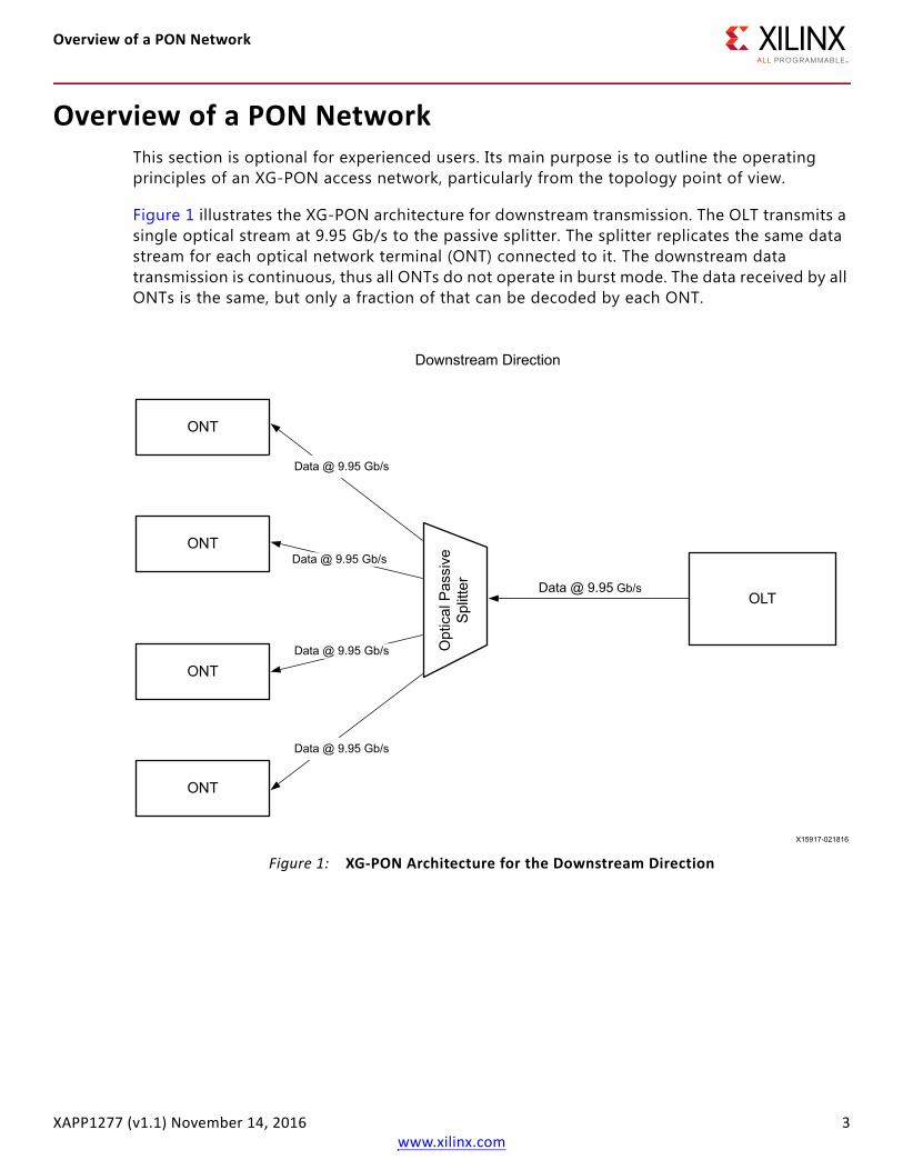
Overview of a PON NetworkThis section is optional for experienced users. Its main purpose is to outline the operating principles of an XG-PON access network, particularly from the topology point of view.
Figure 1 illustrates the XG-PON architecture for downstream transmission. The OLT transmits a single optical stream at 9.95 Gb/s to the passive splitter. The splitter replicates the same data stream for each optical network terminal (ONT) connected to it. The downstream data transmission is continuous, thus all ONTs do not operate in burst mode. The data received by all ONTs is the same, but only a fraction of that can be decoded by each ONT.
X-Ref Target - Figure 1
Figure 1: XG-PON Architecture for the Downstream Direction
OLT
Opt
ical
Pas
sive
Spl
itter Data @ 9.95 Gb/s
Data @ 9.95 Gb/s
Data @ 9.95 Gb/s
Data @ 9.95 Gb/s
ONT
ONT
ONT
ONT
Downstream Direction
Data @ 9.95 Gb/s

Overview of a PON Network
XAPP1277 (v1.1) November 14, 2016 4www.xilinx.com
Figure 2 shows how each ONT recovers the clock embedded into the received data, cleans it up, and reuses it to clock the upstream transmission. The raw upstream speed is 2.488 Gb/s. Each ONT transmits data at the same frequency, as it synchronizes to the downstream link. However, data from different ONTs arrive at the OLT at a phase that is completely uncontrolled and varies significantly over time and temperature. To avoid collision, each ONT must send data only during its permitted time slot. The media time sharing across ONTs is managed by the OLT media access control (MAC) layer.
When a new ONT is allowed to send data to the OLT, the BCDR acquires its phase and extracts the raw data in each burst. Each burst allocates adequate time to:
• Acquire the sampling phase. This is the typical task of the BCDR.
• Identify a start and end-of-packet to identify the packet boundary.
• Allow guard time for ONTs to power their laser sources on and off.
• Allow the automatic gain equalizer in the OLT to settle, because ONTs adjacent in time can be physically far apart.
• Allow AC coupling to charge (if present).
All these contributions negatively affect the efficiency of the upstream direction. Note that the OLT designer controls all these contributions. That is why the OLT design is critical and defines
X-Ref Target - Figure 2
Figure 2: XG-PON Architecture for the Upstream Direction
OLT
Opt
ical
Pas
sive
Spl
itter Data @ 2.488 Gb/s
Data @ 2.488 Gb/s
Data @ 2.488 Gb/s
Data @ 2.488 Gb/s
ONT
ONT
ONT
ONT
Upstream Direction
Data @ 2.488 Gb/s
BCDR

Overview of a PON Network
XAPP1277 (v1.1) November 14, 2016 5www.xilinx.com
the overall efficiency of the PON line. The downstream direction is a continuous transmission and is thus much more efficient than the upstream direction. This architectural limitation fits very well with the application requirement, because users generally require more bandwidth in the downstream direction than upstream. Figure 3 shows the data flow in both the downstream and upstream directions. It highlights the preamble, which is only required for upstream transmission. In general, the preamble is a periodic repetition of the 10-bit pattern. This pattern allows maximizing statistical information in the preamble to optimize overall upstream efficiency. A different preamble pattern can be detected by the BCDR. The length of the pattern is set by the OLT (and provisioned to all ONTs) to a value that allows its BCDR to acquire the burst phase. The bottom part of Figure 3 shows an example configuration of ONT phases as they appear to the BCDR.
RECOMMENDED: Although the BCDR in this application note can detect any preamble length, it is recommended to keep the preamble to a length of at least 32 bits to provide adequate phase information during burst phase acquisition. (ITU-T G.987.2 recommends having at least 160 bits for 1.25G or 48 bits for 1.25G, thus 32 bits is adequate for both cases.
X-Ref Target - Figure 3
Figure 3: Data Flow in the Upstream and Downstream Direction
OLT
Downstream Direction
ONT 1
Upstream Direction
ONT 2 ONT 3
Pac
ket P
hase
Preamble
Phase 1Packet 1
Phase 2Packet 2
Phase 3Packet 3
Time

Circuit Description and Usage Model
XAPP1277 (v1.1) November 14, 2016 6www.xilinx.com
Circuit Description and Usage ModelFigure 4 illustrates the BCDR architecture, showing the relevant inputs and outputs. The deserialized data (32- or 80-bit wide) flows in parallel into the lower branch (LB) and the upper branch (UB).
The lower branch works on delayed data, continuously tuning the numerically controlled oscillator (NCO) to track the incoming data edges. Each raw sample is associated with a phase between –180 degrees and +180 degrees. The raw sample with the phase closest to 0 degrees (that is, closest to the middle of the eye diagram) is extracted by the sample selector block. The lower branch tracks phase variations with typical time constants that are much longer than the preamble time. Thus, the loop in the lower branch is expected to track phase changes or jitter, but not bursts.
The delay element allows the upper branch to recognize a preamble and estimate its phase by averaging the phase information of many consecutive edges. Upon recognizing the consecutive edges as a preamble, the NCO in the lower branch is steered in one single clock cycle to be aligned with the new packet.
The lower branch never experiences a phase burst because the NCO is steered just before the burst enters the phase detector in the lower branch.
For debugging purposes, you can disable the burst injection capability by setting BURST_EN to 0. BCDR Simulation Test Bench further describes this item, which is the characterizing feature of
X-Ref Target - Figure 4
Figure 4: BCDR Simplified Architecture
PhaseDetector
Preamble Detector
BurstPhase
Delay PD LPF NCO
Upper Branch
DIN
PL_O
Sample Selector
PAT_MSK BURST_EN CENTER_F
BURST_EN
PL_IN
Pre
ambl
e P
hase
PHASE_OUT
DT_OUT
DV_OUT
LTR VCO_CTRL
CLK
RST
ENFractional BCDR
Lower Branch
EN

Circuit Description and Usage Model
XAPP1277 (v1.1) November 14, 2016 7www.xilinx.com
a BCDR. The phase of the NCO can be monitored over time for debug purposes, both in simulation and in hardware, through the signal PHASE_OUT.
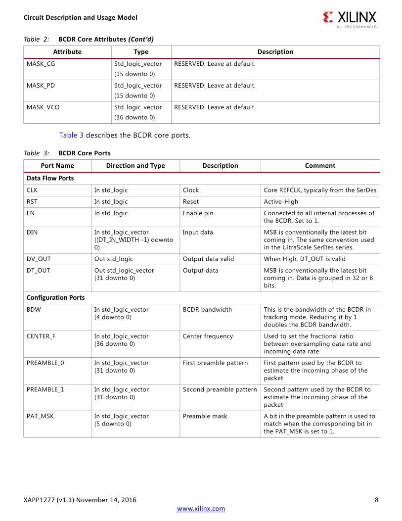
Table 2 describes the attributes of the BCDR core.
Table 2: BCDR Core Attributes
Attribute Type Description
DT_IN_WIDTH Integer Input datapath width. Can be 32 or 80.
DT_OUT_WIDTH Integer Output datapath width. Can be 8 or 32.
ENABLE_CENTER_F_ATTR Std_logic When set to 1, CENTER_F_ATTR is used as CENTER_F.
When set to 0, the CENTER_F port is used.
CENTER_F_ATTR Std_logic_vector
(36 downto 0)
The CENTER_F_ATTR is used when ENABLE_CENTERF_ATTR is set to 1.
EN_PAT_MSK_ATTR Std_logic When set to 1, PAT_MSK_ATTR is used as PAT_MSK.
When set to 0, the PAT_MSK port is used.
PAT_MSK_ATTR Std_logic_vector
(31 downto 0)
The PAT_MSK_ATTR attribute is used when EN_PAT_MSK_ATTR is set to 1.
EN_AVE_SEL_ATTR Std_logic When set to 1, AVE_SEL_ATTR is used as AVE_SEL.
When set to 0, the AVE_SEL port is used.
AVE_SEL_ATTR Std_logic_vector
(1 downto 0)
The AVE_SEL_ATTR is used when EN_AVE_SEL_ATTR is set to 1.
EN_BDW_ATTR Std_logic When set to 1, BDW_ATTR is used as BDW.
When set to 0, the BDW port is used.
BDW_ATTR Std_logic_vector
(3 downto 0)
The BDW_ATTR attribute is used when EN_BDW_ATTR is set to 1.
ENABLE_EN Std_logic When set to 1, the EN port is active for all internal processes.
EN_LTR_PORT Std_logic When EN_LTR_PORT is set to 1, the LTR port is used to disable the lower branch.
When EN_LTR_PORT is set to 0, the lower branch is disabled.
ENABLE_DBG Std_logic When set to 1, debug output ports are enabled.
REDUCE_PD Std_logic When set to 1, allows resource reduction only in 10X mode.
USE_RED_BRICK Std_logic When set to 1, allows resource reduction only in 10X mode.
EN_PREAMBLE_ATTR Std_logic When set to 1, PREAMBLE_ATTR_0 and PREAMBLE_ATTR_1 are used as PREAMBLES.
When set to 0, the PREAMBLE_0 and PREAMBLE_1 ports are used.
PREAMBLE_ATTR_0 Std_logic_vector
(31 downto 0)
The PREAMBLE_ATTR_0 and PREAMBLE_ATTR_1 are used when EN_PREAMBLE_ATTR is set to 1.
PREAMBLE_ATTR_1 Std_logic_vector
(31 downto 0)
The PREAMBLE_ATTR_0 and PREAMBLE_ATTR_1 are used when EN_PREAMBLE_ATTR is set to 1.
EN_CF_ADD Std_logic RESERVED. Set to 0.
SAM_VALIDS Std_logic_vector
(4 downto 0)
Average number of valid bits per clock cycle. The setting 0 is valid for all cases. Setting this number according to use case allows saving resources.
Circuit Description and Usage Model
XAPP1277 (v1.1) November 14, 2016 8www.xilinx.com
Table 3 describes the BCDR core ports.
MASK_CG Std_logic_vector
(15 downto 0)
RESERVED. Leave at default.
MASK_PD Std_logic_vector
(15 downto 0)
RESERVED. Leave at default.
MASK_VCO Std_logic_vector
(36 downto 0)
RESERVED. Leave at default.
Table 2: BCDR Core Attributes (Cont’d)
Attribute Type Description
Table 3: BCDR Core Ports
Port Name Direction and Type Description Comment
Data Flow Ports
CLK In std_logic Clock Core REFCLK, typically from the SerDes
RST In std_logic Reset Active-High
EN In std_logic Enable pin Connected to all internal processes of the BCDR. Set to 1.
DIN In std_logic_vector ((DT_IN_WIDTH -1) downto 0)
Input data MSB is conventionally the latest bit coming in. The same convention used in the UltraScale SerDes series.
DV_OUT Out std_logic Output data valid When High, DT_OUT is valid
DT_OUT Out std_logic_vector (31 downto 0)
Output data MSB is conventionally the latest bit coming in. Data is grouped in 32 or 8 bits.
Configuration Ports
BDW In std_logic_vector (4 downto 0)
BCDR bandwidth This is the bandwidth of the BCDR in tracking mode. Reducing it by 1 doubles the BCDR bandwidth.
CENTER_F In std_logic_vector (36 downto 0)
Center frequency Used to set the fractional ratio between oversampling data rate and incoming data rate
PREAMBLE_0 In std_logic_vector (31 downto 0)
First preamble pattern First pattern used by the BCDR to estimate the incoming phase of the packet
PREAMBLE_1 In std_logic_vector (31 downto 0)
Second preamble pattern Second pattern used by the BCDR to estimate the incoming phase of the packet
PAT_MSK In std_logic_vector (5 downto 0)
Preamble mask A bit in the preamble pattern is used to match when the corresponding bit in the PAT_MSK is set to 1.
Circuit Description and Usage Model
XAPP1277 (v1.1) November 14, 2016 9www.xilinx.com
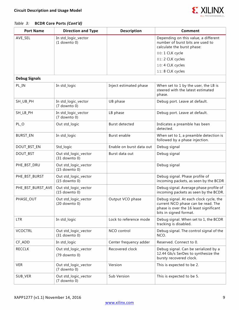
AVE_SEL In std_logic_vector (1 downto 0)
Depending on this value, a different number of burst bits are used to calculate the burst phase:
00: 1 CLK cycle
01: 2 CLK cycles
10: 4 CLK cycles
11: 8 CLK cycles
Debug Signals
PL_IN In std_logic Inject estimated phase When set to 1 by the user, the LB is steered with the latest estimated phase.
SH_UB_PH In std_logic_vector (7 downto 0)
UB phase Debug port. Leave at default.
SH_LB_PH In std_logic_vector (7 downto 0)
LB phase Debug port. Leave at default.
PL_O Out std_logic Burst detected Indicates a preamble has been detected.
BURST_EN In std_logic Burst enable When set to 1, a preamble detection is followed by a phase injection.
DOUT_BST_EN Std_logic Enable on burst data out Debug signal
DOUT_BST Out std_logic_vector (31 downto 0)
Burst data out Debug signal
PHE_BST_DRU Out std_logic_vector (15 downto 0)
Debug signal
PHE_BST_BURST Out std_logic_vector (15 downto 0)
Debug signal. Phase profile of incoming packets, as seen by the BCDR
PHE_BST_BURST_AVE Out std_logic_vector (15 downto 0)
Debug signal. Average phase profile of incoming packets as seen by the BCDR.
PHASE_OUT Out std_logic_vector (20 downto 0)
Output VCO phase Debug signal. At each clock cycle, the current NCO phase can be read. The phase is over the 16 least significant bits in signed format.
LTR In std_logic Lock to reference mode Debug signal. When set to 1, the BCDR tracking is disabled.
VCOCTRL Out std_logic_vector (31 downto 0)
NCO control Debug signal. The control signal of the NCO.
CF_ADD In std_logic Center frequency adder Reserved. Connect to 0.
RECCLK Out std_logic_vector
(79 downto 0)
Recovered clock Debug signal. Can be serialized by a 12.44 Gb/s SerDes to synthesize the bursty recovered clock.
VER Out std_logic_vector (7 downto 0)
Version This is expected to be 2.
SUB_VER Out std_logic_vector (7 downto 0)
Sub Version This is expected to be 5.
Table 3: BCDR Core Ports (Cont’d)
Port Name Direction and Type Description Comment

Circuit Description and Usage Model
XAPP1277 (v1.1) November 14, 2016 10www.xilinx.com
Additional insights on the BCDR ports and their usage follow. The oversampled and deserialized data enters from DIN and exits from DT_OUT. The output DT_OUT is valid only when DV_OUT is 1.
PL_O is a debug signal that the BCDR pulses to 1 each time it detects a preamble. If a preamble is detected, the NCO is steered to the estimated phase only if BURST_EN is set to 1, which is the default condition.
BDW or BDW_ATTR control the bandwidth of the BCDR during tracking—higher values correspond to lower bandwidth.
BCDR and PHY ConfigurationThe BCDR circuit described in this section is designed and tested to work in one of the five different cases specified in Table 4. Preset the BCDR to operate in the desired case by setting attributes and input ports of the BCDR as described in Table 4 and Table 5.
Table 4: Five Possible Operating Conditions and Their Attribute Settings
Attribute Name Case 1 Case 2 Case 3 Case 4 Case 5
DT_IN_WIDTH 80 80 80 32 32
DT_OUT_WIDTH 32 32 32 8 8
ENABLE_CENTER_F_ATTR 1 1 1 1 1
CENTER_F_ATTR H800000000 H1000000000 H55555555 H555555555 H666666666
EN_PAT_MSK_ATTR 1
PAT_MSK_ATTR 100000
EN_AVE_SEL_ATTR 1
AVE_SEL_ATTR 01
EN_BDW_ATTR 1
BDW_ATTR 01010
ENABLE_EN 0
ENABLE_LTR_PORT 0
ENABLE_DBG 1
REDUCE_PD 1 0 0 0 0
USE_RED_BRICK 1 0 0 0 0
EN_PREAMBLE_ATTR 1
PREAMBLE_ATTR_0 HAAAAAAAA
PREAMBLE_ATTR_1 HAAAAAAAA
EN_CF_ADD 0
SAM_VALIDS 00000
MASK_CG HFFF0
MASK_PD HFFF0
MASK_VCO H1FFFFFFFF0
Circuit Description and Usage Model
XAPP1277 (v1.1) November 14, 2016 11www.xilinx.com
The BCDR processes oversampled data from a PHY, which is a SerDes. This has to be configured in lock to reference mode, and its auto-adapting equalizer should be disabled. To do that, set the following ports as listed:
• RXCDRHOLD = 1
• RXLPMHFOVRDEN =1
• RXLPMLFKLOVRDEN=1
• RXOSOVRDEN=1
All these ports are available in the above-mentioned test bench, through virtual input/output (VIO), to properly set the receive CDR and equalizer.
The following section guides you in configuring the GTH SerDes using the UltraScale FPGA Transceiver Wizard in the IP Catalog.
RECOMMENDED: Download the most up-to-date IP update before using the wizard. Details on how to use this wizard can be found in the UltraScale FPGAs Transceivers Wizard: LogiCORE IP Product Guide (PG182) [Ref 3].
Table 5: Port Settings for All Possible Cases
Input Port Name Setting for All Cases
BURST_EN 1
PL_IN 0
SH_UB_PH 00000000
SH_LB_PH 00000000
LTR 0
Circuit Description and Usage Model
XAPP1277 (v1.1) November 14, 2016 12www.xilinx.com
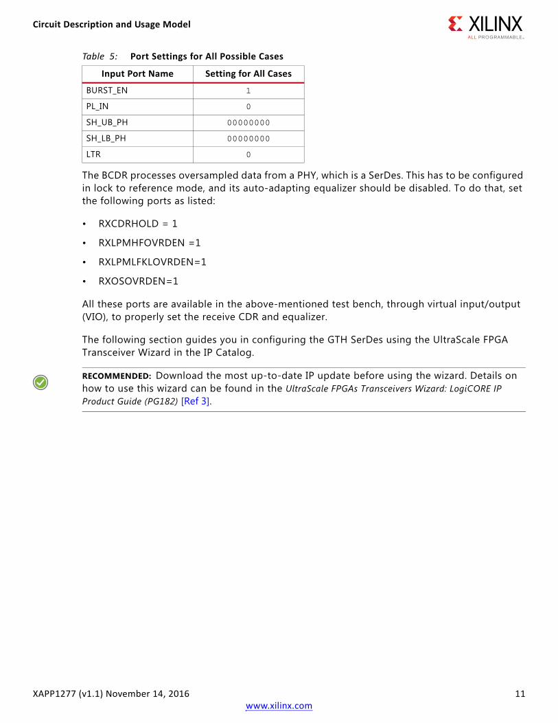
The Basic tab should be configured as shown in Figure 5.
In Figure 5, the RX line rate should be set according to the use case as specified in Table 6.
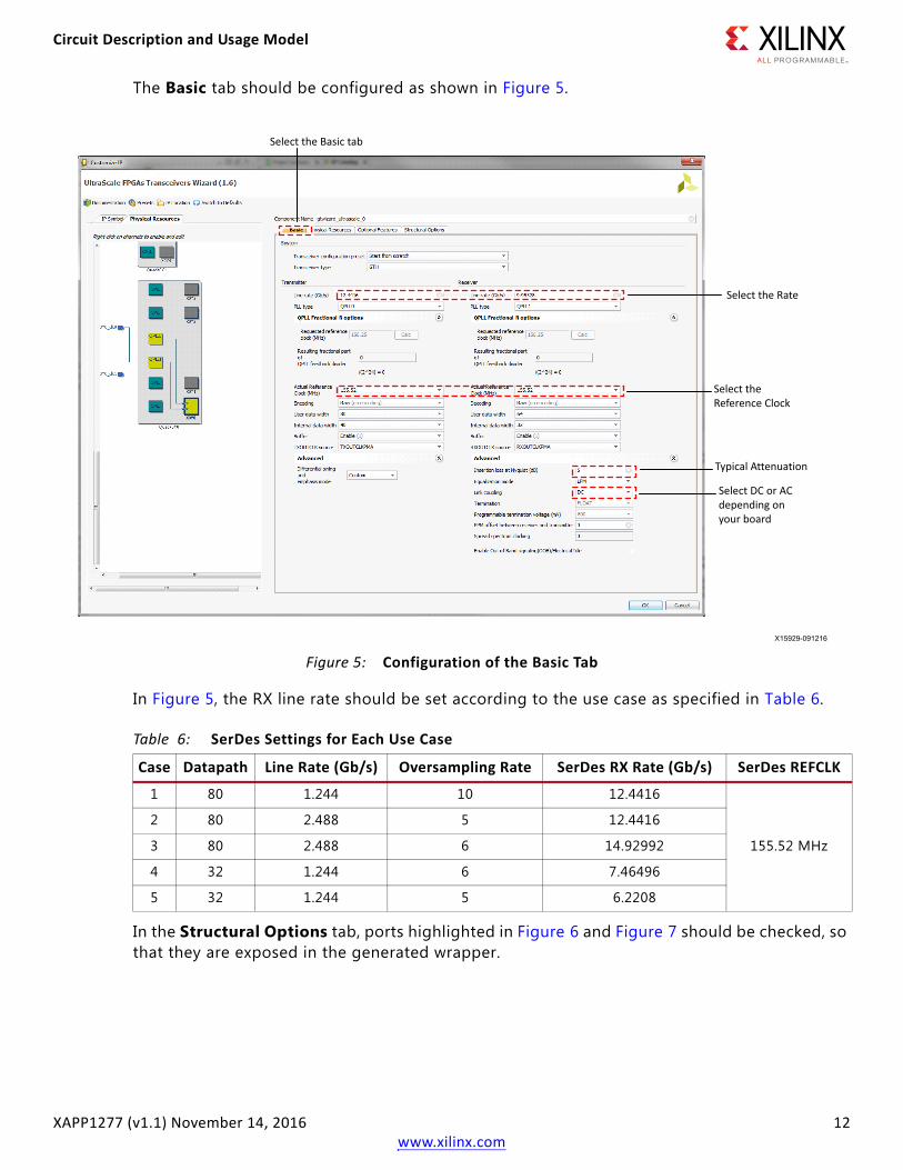
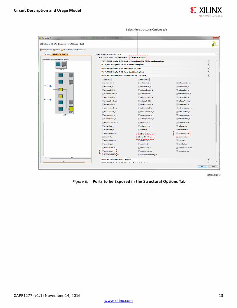
In the Structural Options tab, ports highlighted in Figure 6 and Figure 7 should be checked, so that they are exposed in the generated wrapper.
X-Ref Target - Figure 5
Figure 5: Configuration of the Basic Tab
Select the Basic tab
Select the Rate
Select the Reference Clock
Typical Attenuation
Select DC or AC depending on your board
Table 6: SerDes Settings for Each Use Case
Case Datapath Line Rate (Gb/s) Oversampling Rate SerDes RX Rate (Gb/s) SerDes REFCLK
1 80 1.244 10 12.4416
155.52 MHz
2 80 2.488 5 12.4416
3 80 2.488 6 14.92992
4 32 1.244 6 7.46496
5 32 1.244 5 6.2208
Circuit Description and Usage Model
XAPP1277 (v1.1) November 14, 2016 13www.xilinx.com
X-Ref Target - Figure 6
Figure 6: Ports to be Exposed in the Structural Options Tab
Select the Structural Options tab
BCDR Simulation Test Bench
XAPP1277 (v1.1) November 14, 2016 14www.xilinx.com
BCDR Simulation Test Bench
Start the SimulationTo start the simulation:
1. In a DOS window, change directory to script:
cd /script
2. Start Modelsim:
Modelsim
3. Execute the runsim.do script from within ModelSim:
do run_sim.do
The simulation script compiles all test bench files, runs the simulation, and configures the waveform viewer to show the simulation signals.
X-Ref Target - Figure 7
Figure 7: Additional Ports to be Exposed in the Structural Options Tab
Select the Structural Options tab

BCDR Simulation Test Bench
XAPP1277 (v1.1) November 14, 2016 15www.xilinx.com
Simulation Test ResultsThe remaining part of this section familiarizes you with the simulation test bench outcome, which requires an understanding of the test bench architecture.
The simulation test bench block diagram (Figure 8) includes:
• A G-PON-like pattern generator
° It can be programmed to operate at 1.25 Gb/s or 2.5Gbit/s.
• An ideal serializer (emulating the SerDes transmitter in the ONT).
• An ideal deserializer (emulating the SerDes receiver, in lock to reference mode).
• A G-PON-like pattern checker.
• An optional section that regenerates the bursty recovered clock for debugging.
Ideal serializers and deserializers are used in place of the real SerDes models to make the simulation platform independent and to speed up simulation times.
The structure of the G-PON-like frame is shown in Figure 9.
The G-PON-like pattern generator generates frames that start with a preamble and a start of frame (SOF), followed by a 16-bit counter that increases at each frame and wraps around. The payload is a truncated PRBS 7 pattern. Although any PRBS pattern can be selected for the payload, PRBS 7 has been chosen to avoid SOF/EOF emulation during the payload.
The preamble has 48 bits with alternating 1 and 0 values. The preamble length is user-programmable through the port PREAMBLE_LENGTH, with 1-bit resolution. The pattern
X-Ref Target - Figure 8
Figure 8: Burst BCDR Test Bench Architecture Block Diagram
X-Ref Target - Figure 9
Figure 9: G-PON-like Packet Used to Stress the BCDR
GPON-like Packet
Generator
Payload Error
IdealSerializer
IdealDeserializer
BCDR(DUT)
GPON-like Packet
CheckerFrame Number
IdealSerializer
Bursty RecoveredClock
Optional Debug Section
Preamble SOF Counter Payload (PRBS) EOF
Packet Structure

BCDR Simulation Test Bench
XAPP1277 (v1.1) November 14, 2016 16www.xilinx.com
start is an interleaved version of F628 fixed at 32 bits in length. Some fixed zeros are implemented to prevent the counter emulating the start of the pattern.
Note: The pattern start value of F628 has been conventionally chosen from the synchronous digital hierarchy (SDH) world and is not used by the BCDR to sync.
The test bench is managed by the attribute SIM_CASE in the script run_sim.do per Table 7.
Any bit error is detected by the truncated PRBS 7 error checker. The output PAYLOAD_ERR (from the pattern checker) counts the errors detected by the pattern checker. This counter can be reset at any time by pulsing asynchronously RES_PAYLOAD_ERR. The pattern checker continuously compares the received data to a standard PRBS7 for debugging purposes. The outputs PRBS_ERR and RES_PRBS_ERR serve this purpose.
The frame counter is used by the G-PON-like packet checker to identify the condition when one or more packets have been skipped. This condition is indicated by the line FRAME_ERR being pulsed to 1. The signal FRAME_ALIGN is always NOT(FRAME_ERR) and is thus a redundant signal.
The signals displayed in the simulation window are described first. After, the simulation results are commented (see Table 8).
Table 7: SIM_CASE Attribute Decoding
SIM_CASE Upstream Rate (Gb/s) Oversampling Ratio
1 1.25 10
2 2.5 5
3 2.5 6
4 1.25 5
5 1.25 6
Table 8: Description of Simulation Signals
SIGNAL NAME TYPE DESCRIPTION
SIM_CASE ATTRIBUTE - TOP_LEVEL See Table 1.
RES_PAYLOAD_ERR ASINCHRONOUS INPUT - Pattern Checker
When set to 1, the PAYLOAD_ERR is set to 0.
RES_PRBS_ERR ASINCHRONOUS INPUT - Pattern Checker
When set to 1, the PRBS_ERR is set to 0.
PAYLOAD_ERR OUTPUT - Pattern Checker Number of errors detected in the G-PON-like pattern.
PRBS_ERR OUTPUT - Pattern Checker Number of errors detected in the PRBS pattern.
PREAMBLE_LENGHT SYNCHRONOUS INPUT - Pattern Generator
The preamble length can be set to any value between 0 and 65535.
FRAME_ALIGN OUTPUT - Pattern Checker This signal is set to 1 by the G-PON-like pattern checker when the packet number is consistent with the packet number in the previous packet.
FR_LOSS OUTPUT - Pattern Checker This is always NOT (FRAME_ALIGN) and is thus a redundant indication.

BCDR Simulation Test Bench
XAPP1277 (v1.1) November 14, 2016 17www.xilinx.com
The simulation is divided in 2 parts:
• Up to about 1.5 ms, the signal BURST_EN is set to 0 (debug condition).
• Afterwards, it is set to 1 (default).
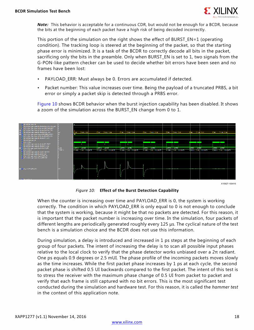
The first part of the simulation shows how the BCDR behaves when the burst injection capability has been disabled. Figure 10 is a detail of the simulation across the BURST_EN change from 0 to 1.
On the left half of the simulation, burst detection capability is not active (debug condition). Note the phase error (in violet) being reduced with an exponential transient by the tracking loop in the lower branch. The pink trace is the phase profile of the incoming data, as seen by the BCDR. On the right side, the preamble detector is active and the NCO is steered at the beginning of each packet to the phase of the incoming data. The phase error is always kept close to 0 by the tracking loop.
BURST_EN INPUT - BCDR When set to 0, the burst detection capability of the BCDR is disabled. This is a debug condition. This signal is connected directly to the BURST_EN input of the BCDR core.
DT_IN INPUT - BCDR Deserialized oversampled data, from the ideal deserializer.
FR_START OUTPUT - Pattern Checker It marks the frame start as seen by the G-PON-like packet checker.
FR_END OUTPUT - Pattern Checker It marks the frame end as seen by the G-PON-like packet checker.
FR_NM OUTPUT - Pattern Checker Frame number as seen by the G-PON-like packet checker. A skipped packet always produces bit errors and forces the FRAME_ALIGN to temporarily go to 0.
rit_int TIME Transport delay applied to DT_IN.
EN_HAMMER INPUT - Pattern Generator When set to 1, consecutive transmitted packets have 0.5 unit interval (UI) phase difference.
EN_RIT INPUT - Pattern Generator EN_RIT is for simulation only. Enables hammer testing and shifts all packets by 1 ps every 4 packets. The condition EN_RIT and EN_HAMMER is not allowed.
PRBS_EN INPUT - Pattern Generator When set to 1, the transmitted pattern is a PRBS 7.
ERR_INS ASINCHRONOUS INPUT - Pattern Generator
Flips one bit in the transmitted data pattern, PRBS or G-PON-like.
PHE_BST_DRU SIGNED OUTPUT - BCDR This is the phase error of the incoming data.
PHE_BST_BURST SIGNED OUTPUT - BCDR This is the phase profile of the incoming data as seen by the BCDR.
PHE_BURST_AVE SIGNED OUTPUT - BCDR Average of the above signal PHE_BURST.
PL_O OUTPUT - BCDR When set to 1 by the BCDR, a preamble has been detected.
Table 8: Description of Simulation Signals (Cont’d)
SIGNAL NAME TYPE DESCRIPTION
BCDR Simulation Test Bench
XAPP1277 (v1.1) November 14, 2016 18www.xilinx.com
Note: This behavior is acceptable for a continuous CDR, but would not be enough for a BCDR, because the bits at the beginning of each packet have a high risk of being decoded incorrectly.
This portion of the simulation on the right shows the effect of BURST_EN=1 (operating condition). The tracking loop is steered at the beginning of the packet, so that the starting phase error is minimized. It is a task of the BCDR to correctly decode all bits in the packet, sacrificing only the bits in the preamble. Only when BURST_EN is set to 1, two signals from the G-PON-like pattern checker can be used to decide whether bit errors have been seen and no frames have been lost:
• PAYLOAD_ERR: Must always be 0. Errors are accumulated if detected.
• Packet number: This value increases over time. Being the payload of a truncated PRBS, a bit error or simply a packet skip is detected through a PRBS error.
Figure 10 shows BCDR behavior when the burst injection capability has been disabled. It shows a zoom of the simulation across the BURST_EN change from 0 to 1.
When the counter is increasing over time and PAYLOAD_ERR is 0, the system is working correctly. The condition in which PAYLOAD_ERR is only equal to 0 is not enough to conclude that the system is working, because it might be that no packets are detected. For this reason, it is important that the packet number is increasing over time. In the simulation, four packets of different lengths are periodically generated roughly every 125 μs. The cyclical nature of the test bench is a simulation choice and the BCDR does not use this information.
During simulation, a delay is introduced and increased in 1 ps steps at the beginning of each group of four packets. The intent of increasing the delay is to scan all possible input phases relative to the local clock to verify that the phase detector works unbiased over a 2π radiant. One ps equals 0.9 degrees or 2.5 mUI. The phase profile of the incoming packets moves slowly as the time increases. While the first packet phase increases by 1 ps at each cycle, the second packet phase is shifted 0.5 UI backwards compared to the first packet. The intent of this test is to stress the receiver with the maximum phase change of 0.5 UI from packet to packet and verify that each frame is still captured with no bit errors. This is the most significant test conducted during the simulation and hardware test. For this reason, it is called the hammer test in the context of this application note.
X-Ref Target - Figure 10
Figure 10: Effect of the Burst Detection Capability
Hardware Test Bench on the KCU1250 Board
XAPP1277 (v1.1) November 14, 2016 19www.xilinx.com
Hardware Test Bench on the KCU1250 BoardThe hardware test bench is designed for the KCU1250 characterization board. (The KCU705 evaluation board can also be used for this purpose, but the AC coupling on the board prevents testing the BCDR at very low preamble lengths.)
Connect a Bulls Eye® cable to Q226, and refclk_0 should be connected to a 155.52 MHz reference clock. This is the only clock that is used by the test bench. In Q226, the transmitter of channel 3 should be connected to the receiver of channel 3, in DC-coupled mode.
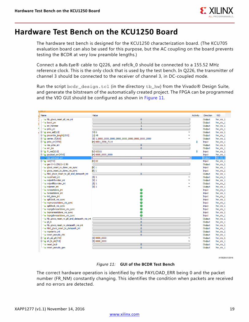
Run the script bcdr_design.tcl (in the directory tb_hw) from the Vivado® Design Suite, and generate the bitstream of the automatically created project. The FPGA can be programmed and the VIO GUI should be configured as shown in Figure 11.
The correct hardware operation is identified by the PAYLOAD_ERR being 0 and the packet number (FR_NM) constantly changing. This identifies the condition when packets are received and no errors are detected.
X-Ref Target - Figure 11
Figure 11: GUI of the BCDR Test Bench
Device Sizing and Recommendations
XAPP1277 (v1.1) November 14, 2016 20www.xilinx.com
This test bench can stress the BCDR by setting EN_HAMMER to 1, which identifies the condition where packets have a 0.5 UI phase shift packet to packet.
The preamble length can be programmed on the fly to verify the correct operation of the BCDR, even at very low preamble lengths.
All debug signals from the BCDR can be monitored by an integrated logic analyzer (ILA) core, also present in the hardware test bench.
Device Sizing and RecommendationsThis section describes the resources required by the BCDR, depending on configuration. Detailed required resources can be found in Figure 9.
Reference DesignYou can download the Reference Design Files for this application note from the Xilinx website.
Table 10 shows the reference design matrix.
Table 9: BCDR Size, Depending on Configuration
DT_IN_WIDTH = 80 DT_IN_WIDTH = 32
Resource Type 1.25G only 2.5G only 1.25G and 2.5G 1.25G only
LUT 5,954 11,926 18,269 1,694
FF 6,249 11,463 12,286 1,548
DSP 3 3 3 3
RAMB16 5 5 5 0
Table 10: Reference Design Matrix
Parameter Description
General
Developer name Paolo Novellini, Antonello Di Fresco, and Massimo Chirico
Target devices (stepping level, ES, production, speed grades) Kintex® UltraScale and Virtex® UltraScale FPGAs
Source code provided Yes
Source code format VHDL
Design uses code and IP from existing Xilinx application note reference designs, CORE Generator™ software, or third parties.
No
Simulation
Functional simulation performed Yes

References
XAPP1277 (v1.1) November 14, 2016 21www.xilinx.com
References1. ITU-T G.987 and ITU-T G.989 standards can be downloaded from the ITU website www.itu.int:
° ITU-T G.987, 10-Gigabit-capable passive optical network (XG-PON) systems
° ITU-T G.989, 40-Gigabit-capable passive optical networks (NG-PON2) systems
Note: IEEE Std 802.3av-2009, IEEE Standard Physical Layer Specifications and Management Parameters for 10 Gb/s Passive Optical Networks can be downloaded from the IEEE website [Ref 2].
Note: These PON definitions are from Section 3 of the ITU-T G.989.2 standard [Ref 1]:- 10G EPON - 10 Gb-capable Ethernet passive optical network- G-PON - Gigabit-capable passive optical network- ITU-T - International Telecommunication Union, standardization sector of ITU- NG-PON2 - Next generation PON 2- OLT - Optical line termination- ONT - Optical network terminal- PON - Passive optical network- XG-PON - 10 Gb-capable PON. XG-PON is also called 10G-PON. It realizes NG-PON1.
2. IEEE 802.3av-2009 10 Gbit/s Ethernet Passive Optical Network is part of IEEE Standard for Ethernet IEEE Std 802.3-2012. The next full revision is in IEEE 802.3-2015 (standards.ieee.org/findstds/standard/802.3-2015).
3. UltraScale FPGAs Transceivers Wizard: LogiCORE IP Product Guide (PG182)
Timing simulation performed N/A
Test bench used for functional and timing simulations Yes
Test bench format VHDL
Simulator software/version used Mentor ModelSim 10.4
SPICE/IBIS simulations N/A
Implementation
Synthesis software tools/versions used Vivado Design Suite 2016.2
Implementation software tools/versions used Vivado Design Suite 2016.2
Static timing analysis performed Yes
Hardware Verification
Hardware verified Yes
Hardware platform used for verification KCU1250 characterization board
Table 10: Reference Design Matrix (Cont’d)
Parameter Description

Revision History
XAPP1277 (v1.1) November 14, 2016 22www.xilinx.com
Revision HistoryThe following table shows the revision history for this document.
Please Read: Important Legal NoticesThe information disclosed to you hereunder (the “Materials”) is provided solely for the selection and use of Xilinx products. To the maximum extent permitted by applicable law: (1) Materials are made available "AS IS" and with all faults, Xilinx hereby DISCLAIMS ALL WARRANTIES AND CONDITIONS, EXPRESS, IMPLIED, OR STATUTORY, INCLUDING BUT NOT LIMITED TO WARRANTIES OF MERCHANTABILITY, NON-INFRINGEMENT, OR FITNESS FOR ANY PARTICULAR PURPOSE; and (2) Xilinx shall not be liable (whether in contract or tort, including negligence, or under any other theory of liability) for any loss or damage of any kind or nature related to, arising under, or in connection with, the Materials (including your use of the Materials), including for any direct, indirect, special, incidental, or consequential loss or damage (including loss of data, profits, goodwill, or any type of loss or damage suffered as a result of any action brought by a third party) even if such damage or loss was reasonably foreseeable or Xilinx had been advised of the possibility of the same. Xilinx assumes no obligation to correct any errors contained in the Materials or to notify you of updates to the Materials or to product specifications. You may not reproduce, modify, distribute, or publicly display the Materials without prior written consent. Certain products are subject to the terms and conditions of Xilinx’s limited warranty, please refer to Xilinx’s Terms of Sale which can be viewed at https://www.xilinx.com/legal.htm#tos; IP cores may be subject to warranty and support terms contained in a license issued to you by Xilinx. Xilinx products are not designed or intended to be fail-safe or for use in any application requiring fail-safe performance; you assume sole risk and liability for use of Xilinx products in such critical applications, please refer to Xilinx’s Terms of Sale which can be viewed at https://www.xilinx.com/legal.htm#tos.Automotive Applications DisclaimerAUTOMOTIVE PRODUCTS (IDENTIFIED AS “XA” IN THE PART NUMBER) ARE NOT WARRANTED FOR USE IN THE DEPLOYMENT OF AIRBAGS OR FOR USE IN APPLICATIONS THAT AFFECT CONTROL OF A VEHICLE (“SAFETY APPLICATION”) UNLESS THERE IS A SAFETY CONCEPT OR REDUNDANCY FEATURE CONSISTENT WITH THE ISO 26262 AUTOMOTIVE SAFETY STANDARD (“SAFETY DESIGN”). CUSTOMER SHALL, PRIOR TO USING OR DISTRIBUTING ANY SYSTEMS THAT INCORPORATE PRODUCTS, THOROUGHLY TEST SUCH SYSTEMS FOR SAFETY PURPOSES. USE OF PRODUCTS IN A SAFETY APPLICATION WITHOUT A SAFETY DESIGN IS FULLY AT THE RISK OF CUSTOMER, SUBJECT ONLY TO APPLICABLE LAWS AND REGULATIONS GOVERNING LIMITATIONS ON PRODUCT LIABILITY.© Copyright 2016 Xilinx, Inc. Xilinx, the Xilinx logo, Artix, ISE, Kintex, Spartan, Virtex, Vivado, Zynq, and other designated brands included herein are trademarks of Xilinx in the United States and other countries. All other trademarks are the property of their respective owners.
Date Version Revision
11/14/2016 1.1 Added support for 32-bit BCDR. Instances of GTX transceivers changed to GTH. Updated Figure 1, Figure 4, Figure 5, Figure 8, and Figure 10. Added two cases to Table 1. Updated attribute and port information in Table 2 and Table 3, respectively. Added section BCDR and PHY Configuration. Updated the BCDR Simulation Test Bench section.
02/29/2016 1.0 Initial Xilinx release.