c 798 acta - jultika.oulu.fi
TRANSCRIPT
UNIVERSITY OF OULU P .O. Box 8000 F I -90014 UNIVERSITY OF OULU FINLAND
A C T A U N I V E R S I T A T I S O U L U E N S I S
University Lecturer Tuomo Glumoff
University Lecturer Santeri Palviainen
Postdoctoral researcher Jani Peräntie
University Lecturer Anne Tuomisto
University Lecturer Veli-Matti Ulvinen
Planning Director Pertti Tikkanen
Professor Jari Juga
Associate Professor (tenure) Anu Soikkeli
University Lecturer Santeri Palviainen
Publications Editor Kirsti Nurkkala
ISBN 978-952-62-3035-1 (Paperback)ISBN 978-952-62-3036-8 (PDF)ISSN 0355-3213 (Print)ISSN 1796-2226 (Online)
U N I V E R S I TAT I S O U L U E N S I SACTAC
TECHNICA
U N I V E R S I TAT I S O U L U E N S I SACTAC
TECHNICA
OULU 2021
C 798
Jaakko Huikari
2D CMOS SPAD ARRAY TECHNIQUES IN 1D PULSED TOF DISTANCE MEASUREMENT APPLICATIONS
UNIVERSITY OF OULU GRADUATE SCHOOL;UNIVERSITY OF OULU,FACULTY OF INFORMATION TECHNOLOGY AND ELECTRICAL ENGINEERING
C 798
AC
TAJaakko H
uikari
C798etukansi.fm Page 1 Tuesday, August 17, 2021 2:59 PM

ACTA UNIVERS ITAT I S OULUENS I SC Te c h n i c a 7 9 8
JAAKKO HUIKARI
2D CMOS SPAD ARRAY TECHNIQUES IN 1D PULSED TOF DISTANCE MEASUREMENT APPLICATIONS
Academic dissertation to be presented with the assent ofthe Doctoral Training Committee of InformationTechnology and Electrical Engineering of the University ofOulu for public defence in the OP auditorium (L10),Linnanmaa, on 1 October 2021, at 12 noon
UNIVERSITY OF OULU, OULU 2021

Copyright © 2021Acta Univ. Oul. C 798, 2021
Supervised byProfessor Juha KostamovaaraDocent Jussi-Pekka Jansson
Reviewed byProfessor Viktor KrozerDoctor Markus Henriksson
ISBN 978-952-62-3035-1 (Paperback)ISBN 978-952-62-3036-8 (PDF)
ISSN 0355-3213 (Printed)ISSN 1796-2226 (Online)
Cover DesignRaimo Ahonen
PUNAMUSTATAMPERE 2021
OpponentDocent Markku Åberg
Huikari, Jaakko, 2D CMOS SPAD array techniques in 1D pulsed TOF distancemeasurement applications. University of Oulu Graduate School; University of Oulu, Faculty of Information Technologyand Electrical EngineeringActa Univ. Oul. C 798, 2021University of Oulu, P.O. Box 8000, FI-90014 University of Oulu, Finland
Abstract
The goal of the research was to study the characteristics, performance and feasibility of a pulsedtime-of-flight 1D laser radar system employing a 2D SPAD detector array in conjunction with acustom-made laser diode producing high energy and high-speed laser pulses. The researchincluded the characterization and comparison of custom-made QW and bulk laser diodesoperating in enhanced gain switching mode and producing laser pulses with a total energy of ~1–5nJ and an FWHM of ~100 ps at pulsing rates >100 kHz. The receiver module was a purpose-builtsingle-chip CMOS IC incorporating a 2D 9x9 SPAD array and a 10-channel TDC circuit enablingparallel SPAD-specific TOF measurements.
The key performance parameters of the laser radar system are intrinsic timing walk error ~5cm (dynamic range ~1:100 000), linearity ± 0.5 mm, signal detection rate ~28% (target distance34 m and reflectivity 11%) and precision ~2 cm. The total energy of a probe pulse was 0.6 nJ andthe diameter of the circular receiver aperture ~20 mm. The selectable subarray feature of thereceiver IC enables laser spot tracking on the detector array while maintaining a small effectivefield of view, thus reducing background radiation-induced noise detections, and offering prospectof walk error free measurement results. Detection time gating proved an effective means forsignal-to-noise ratio improvement under conditions of high-level background radiation.Feasibility studies demonstrated high spatial accuracy of the system in practical settings whenperforming non-contact human heart rate measurement and when distinguishing individual free-falling snowflakes.
The implementation and performance of the 1D laser radar system demonstrated the viabilityof the proposed technology as an alternative along with a conventional laser radar operating in thelinear detection mode for high performance, compact and cost-effective laser radar applications.
Keywords: 1D laser range finding, 2D SPAD detector array, pulsed time-of-flight, sub-ns laser pulse

Huikari, Jaakko, 2D CMOS SPAD-ilmaisinmatriisi laserpulssin lentoaikaanperustuvassa 1D-etäisyysmittauksessa. Oulun yliopiston tutkijakoulu; Oulun yliopisto, Tieto- ja sähkötekniikan tiedekuntaActa Univ. Oul. C 798, 2021Oulun yliopisto, PL 8000, 90014 Oulun yliopisto
Tiivistelmä
Väitöstyössä tutkittiin kaksiulotteista SPAD-ilmaisinmatriisiteknologiaa sekä suurienergisiä jalyhyitä laserpulsseja hyödyntävän 1D-lasertutkan ominaisuuksia, suorituskykyä ja toteutetta-vuutta. Tutkimuksessa karakterisoitiin ja vertailtiin erikoisrakenteisia ”enhanced gain swit-ching”-moodissa toimivia bulk- ja kvanttikaivolaserdiodeja (QW), joilla voidaan tuottaa ~1–5 nJsekä ~100 ps (puoliarvoleveys) laserpulsseja >100 kHz pulssitustahdilla. Tutkimustyössä kehite-tyn ja toteutetun pienikokoisen lasertutkan vastaanottimena käytettiin tarkoitukseen suunniteltuaintegroitua CMOS-piiriä, joka sisältää 9x9 SPAD ilmaisinmatriisin sekä 10-kanavaisen aika-digitaalimuuntimen (TDC) rinnakkaisia SPAD-kohtaisia laserpulssin kulkuaikamittauksia var-ten.
Lasertutkan keskeiset suorituskykyparametrit ovat kompensoimaton ajoitusvirhe ~5 cm(dynaaminen alue ~1:100 000), lineaarisuus ± 0,5 mm, signaalin ilmaisutahti ~28 % (kohteenetäisyys 34 m, heijastuskerroin 11 %) ja kertamittaustarkkuus ~2 cm. Laserpulssin kokonais-energia ja vastaanottimen apertuurin halkaisija ovat 0,6 nJ ja ~20 mm. Aktiivinen 3x3 osailmai-sinmatriisi minimoi vastaanottimen efektiivisen näkökentän (FOV) vähentäen taustasäteilystäaiheutuvia ilmaisuja ja osailmaisinmatriisin valintatoiminto mahdollistaa laserspotin seurannanilmaisinmatriisin pinnalla sekä ajoitusvirheettömät etäisyysmittaustulokset. Ilmaisimen aikapor-titustoimintoa voidaan käyttää mittauksen signaali-kohinasuhteen (SNR) parantamiseen tausta-säteilyn ollessa voimakasta. Lasertutkan spatiaalisen tarkkuuden sekä mittausnopeuden havain-nollistamiseksi suoritetuissa soveltuvuustutkimuksissa mitattiin koehenkilön sydämen sykeilman fyysistä kontaktia usean metrin etäisyydeltä sekä havaittiin yksittäisistä lumihiutaleistaaiheutuvia kaikuja lumisateessa.
Tutkimuksen tuloksiin perustuen kehitetty teknologia on toimiva vaihtoehto ns. perinteisenlineaariseen ilmaisuun perustuvan lasertutkan ohella suorituskykyisiin, kompakteihin ja kustan-nustehokkaisiin lasertutkasovelluksiin.
Asiasanat: 1D-laseretäisyysmittaus, 2D SPAD-ilmaisinmatriisi, pulssin kulkuaika-mittaus, sub-ns laserpulssi


7
Acknowledgements
I would like to express my gratitude to Professor Juha Kostamovaara for the
opportunity to work in his research group and for his supervision of my doctoral
research. I am grateful for all the help and support received from him related to my
studies and to the manuscript for this thesis and not least for his patience during the
project. It has been a privilege to work with and learn from his inspiring personality.
I would also like to thank all the former and current personnel of CAS research
group and others who have contributed their efforts, time and knowledge for the
advancement of this research in one way or another. The following persons and
their contributions especially deserve to be mentioned: Dr. Eugene Avrutin and Dr.
Boris Ryvkin for co-publishing and co-authoring the peer-reviewed papers, Dr.
Lauri Hallman and Dr. Sahba Jahromi for all their help in the laboratory and with
the measurements, Associate Professor Ilkka Nissinen and Docent Jan Nissinen for
their availability and inspiring conversations on research matters, and Matti
Polojärvi for all his technical support in constructing the system and acquiring the
materials.
The manuscript was reviewed by Prof. Dr. Viktor Krozer and Ph.D. Markus
Henriksson prior to publication and the English language of the manuscript was
revised by Malcolm Hicks, M.A. I thank them all for their contributions and
valuable feedback on the thesis.
The research was supported financially by Academy of Finland and Finnish
Funding Agency for Technology and Innovation (TEKES), of which I would like
to express my gratitude.
Finally, I would like to thank my family and friends for all the support I have
received from them in so many ways and for relaxing and inspiring leisure time
pursuits during the years.
Oulu, August 2021 Jaakko Huikari

8

9
List of abbreviations and symbols
1D 1-dimensional
2D 2-dimensional
3D 3-dimensional
APD avalanche photodiode
BiCMOS bipolar complementary metal oxide semiconductor
BPM beats per minute
C capacitance
CFD constant fraction discriminator
CMOS IC complementary metal oxide semiconductor integrated circuit
CR capacitor-resistor
CW continuous wave
DCR dark count rate
DH double heterostucture
EHP electron-hole pair
EMI electromagnetic interference
FF fill factor
FFT fast Fourier transform
FOV field of view
FPGA field-programmable gate array
FWHM full-width-at-half-maximum
GaAs gallium arsenide
AlGaAs aluminum gallium arsenide
GaN gallium nitride
HW hardware
HV CMOS high voltage complementary metal oxide semiconductor
InGaAs indium gallium arsenide
InP indium phosphide
IRF impulse response function
LD laser diode
LiDAR light detection and ranging
Lstray stray inductance
MOSFET metal-oxide semiconductor field-effect transistor
NIR near-infrared
OE opto-electrical (converter)
PCB printed circuit board
10
PDE photon detection efficiency
PIN p-type/intrinsic/n-type
PMT photomultiplier tube
QW quantum well
RLC resistor-inductor-capacitor
RMS root mean square
SBR signal-to-background ratio
SNBGR signal-to-background induced detections ratio
Si silicon
SiPM silicon photomultiplier
SLR single-lens reflex
SNR signal-to-noise ratio
SNSPD superconducting nanowire single-photon detector
SPAD single-photon avalanche diode
TDC time-to-digital converter
TIA trans impedance amplifier
TOF time-of-flight
VCSEL vertical-cavity surface-emitting laser
Ar area of receiver aperture
BWopt optical bandwidth of receiver
c speed of light
Ctot total capacitance
dact active layer thickness
Epho photon energy
Epulse total energy of probe pulse
FOVSPAD linear field of view of SPAD detector element
foptics focal length of receiver optics
fpulse pulsing frequency
h Planck constant
ipeak peak current value
IS solar spectral irradiance
L inductance
Ltot total inductance
n̂ mean number of photons
n̂bg mean number of background photons
Nmeas number of measurement cycles
Nsigdet number of signal photon detections
11
npho number of photons
PBG total power of solar background radiation
pdet probability of background photons induced detection
P(n) probability of occurrence of n photons
R target distance
Rbias bias resistor
Rdamp damping resistor
Rmax maximum unambiguous target distance
Tmean det mean time between photon detections
Tmean pho mean time between photons in background photon flux
tpulse width of probe pulse
tpulse FWHM laser pulse full-width-at-half-maximum
trise probe pulse rise time
tSPAD jitter detection timing jitter of a SPAD element
tTOF laser pulse time-of-flight
Vbias bias voltage
VHV high-voltage supply
VL voltage over an inductor
Γ optical confinement factor
ΔT detection window time interval
Φdet diameter of SPAD element
ϵ target reflectivity
λ emission wavelength
ρtarget target reflectivity
σ standard deviation of number of photons
σsignal RMS noise signal photons
σbg RMS noise background photons
σx̅ standard error of the mean
σdistr the standard deviation of the distribution of measurement results
τ efficiency of optics

12

13
List of original publications
This thesis is based on the following publications, which are referred throughout
the text by their Roman numerals:
I Hallman, L., Huikari, J., & Kostamovaara, J. (2014). A high-speed/power laser transmitter for single photon imaging applications. In IEEE Sensors 2014 Proceedings. IEEE. https://doi.org/10.1109/icsens.2014.6985213
II Huikari, J. M. T., Avrutin, E. A., Ryvkin, B. S., Nissinen, J. J., & Kostamovaara, J. T. (2015). High-energy picosecond pulse generation by gain switching in asymmetric waveguide structure multiple quantum well lasers. IEEE Journal of Selected Topics in Quantum Electronics, 21(6), 1501206. https://doi.org/10.1109/jstqe.2015.2416342
III Kostamovaara, J., Huikari, J., Hallman, L., Nissinen, I., Nissinen, J., Rapakko, H., Avrutin, E., & Ryvkin, B. (2015). On laser ranging based on high-speed/energy laser diode pulses and single-photon detection techniques. IEEE Photonics Journal, 7(2), 7800215. https://doi.org/10.1109/jphot.2015.2402129
IV Huikari, J., Avrutin, E., Ryvkin, B., & Kostamovaara, J. (2016). High-energy sub-nanosecond optical pulse generation with a semiconductor laser diode for pulsed TOF laser ranging utilizing the single photon detection approach. Optical Review, 23, 522–528. https://doi.org/10.1007/s10043-016-0189-7
V Huikari, J., Jahromi, S., Jansson, J.-P., & Kostamovaara, J. (2017). A laser radar based on a “Impulse-like” laser diode transmitter and a 2D SPAD/TDC receiver. In 2017 IEEE International Instrumentation and Measurement Technology Conference (I2MTC). IEEE. https://doi.org/10.1109/i2mtc.2017.7969799
VI Huikari, J., Jahromi, S., Jansson, J.-P., & Kostamovaara, J. (2018). Compact laser radar based on a subnanosecond laser diode transmitter and a two-dimensional CMOS single-photon receiver. Optical Engineering, 57(2), 024104. https://doi.org/10.1117/1.oe.57.2.024104

14

15
Contents
Abstract Tiivistelmä
Acknowledgements 7
List of abbreviations and symbols 9
List of original publications 13
Contents 15
1 Introduction 17
1.1 Background ............................................................................................. 17
1.2 Hypothesis, aims and contributions ........................................................ 19
1.3 Structure of the thesis and its peer reviewed papers ............................... 21
2 Pulsed time-of-flight laser radar 25
2.1 Signal and solar background noise .......................................................... 28
2.2 Photon shot noise and photon statistics ................................................... 31
2.3 Linear detection techniques ..................................................................... 33
2.3.1 Timing walk error and the effect of noise on linear
detection ....................................................................................... 34
2.4 The SPAD technique ............................................................................... 36
2.4.1 Basics of a SPAD detector ............................................................ 37
2.4.2 Walk error and false detections..................................................... 38
2.4.3 Silicon photomultiplier ................................................................. 39
2.5 Single-photon detection and statistical sampling .................................... 40
2.6 High energy and high-speed laser pulses ................................................ 43
3 Literature review 47
4 Laser diode characterization 57
5 Design principles and implementation of a 1D laser radar
employing a SPAD detector array 65
5.1 Transmitter module ................................................................................. 66
5.2 Receiver module ..................................................................................... 68
6 Characterization of the 1D laser radar 73
6.1 Characterization results ........................................................................... 74
6.2 Feasibility studies .................................................................................... 85
7 Discussion 93
8 Summary 99
List of references 103
Original publications 109

16
17
1 Introduction
1.1 Background
Laser radar provides an effective means for high-resolution, long-range 1D
electronic distance measurement. By comparison with its renowned predecessor,
microwave radar, optical laser radar has superior beam directionality, which
accounts for its significantly better spatial resolution. This difference arises from
the fact that laser radiation at around the optical wavelength region has several
orders of magnitude shorter wavelengths, resulting in significantly smaller
diffraction-limited spot sizes in the optical system (Carmer & Peterson, 1996),
which will enable the projection of a large amount of tightly spatially concentrated
energy at the distant target by collimating the laser beam by means of an ordinary
optical lens. In addition, the narrow line width of the laser emission will enable the
use of narrow optical band pass filtering in the receiver as an effective means of
decreasing the noise induced by background radiation (Svelto, 1998, p. 9).
The operating principle of pulsed time-of-flight (TOF) laser radar is based on
accurate measurement of the flight time of a laser pulse to the target and back
(Donati, 2004). Typical real-world targets are non-cooperative, i.e. diffuse, in
nature, so that the magnitude of the laser pulse echo from the target weakens rapidly
with increasing distance (Pedrotti & Pedrotti, 1993, p. 11). Obvious ways of
compensating for the serious issue of photon scarcity in laser radar applications are
to increase the power of the laser pulse, the sensitivity of the photodetector and the
size of the receiver aperture.
Typical photodetectors employed in pulsed TOF laser radars so far have been
PIN diodes and avalanche photodiodes (APD), i.e. types of linear photodetector
that characteristically generate an electrical signal which is in principle analogous
to an optical input signal (McIntyre, 1970). Of the two, an APD detector is a
practical combination of high photon sensitivity, high-speed and low noise
characteristics and is typically preferred over a PIN diode for photon-starved
applications such as laser radar (Muoi, 1984). An APD detector involves the use of
an analogue receiver channel featuring a wideband trans-impedance amplifier with
high gain and low noise, the designing and implementation of which is by no means
a trivial task. The width of the probe pulse employed in these laser radar systems is
customarily a few nanoseconds, arising from the fact that it is relatively
straightforward in practice to implement a current pulse of that width with
18
sufficient amplitude (i.e. 10–30 A) to drive the laser diode (Vainshtein, Yuferev, &
Kostamovaara, 2002).
The single-photon avalanche diode (SPAD) has recently become an
increasingly viable alternative to serve as the photodetector element of a pulsed
TOF laser radar system. Along with its most notable performance characteristics,
extreme photon sensitivity, i.e. down to a single photon, and a detection timing
precision of <100 ps (Pancheri & Stoppa, 2007), the silicon SPAD element
fabrication process has been compatible with the standard complementary metal
oxide semiconductor (CMOS) integrated circuit technology since the early 2000s
(Rochas, Besse, & Popovic, 2001). Another feature speaking in favour of the SPAD
approach is its distinctive nonlinear photon detection mechanism. The sudden
avalanche breakdown of a backward-biased p-n junction caused by absorption of a
photon generates a digital-like output signal signifying the photon detection timing
(Cova, Ghioni, Lacaita, Samori, & Zappa, 1996), thus requiring only very simple
receiver electronics. The above has opened up the prospect of a compact receiver
module integrated on a single CMOS chip containing a 2D SPAD detector array
structure, the associated electronics and a TOF interval measurement circuit, which
has been under intense study by several research groups and has been employed
chiefly in 3D laser radar applications. (Albota et al., 2002; Niclass, Soga,
Matsubara, Kato, & Kagami, 2013; Ruokamo, Hallman, & Kostamovaara, 2019).
Ironically, however, the main weakness of the SPAD detector is an inescapable
side effect associated with one of its strengths, which may become particularly
problematic in laser radar applications exposed to high-level background radiation,
as is often the case outdoors. Due to the extreme photon sensitivity of the SPAD
detector, any photon incident to it, whether from a probe signal or from background
radiation, may cause an avalanche breakdown, thus masking the signal photons
from detection and in the worst case of high background radiation, causing a total
blockage of the detector (Paper III). Thus background radiation can place serious
practical limitations on the employment of single-photon detectors in applications
exposed to high-level background radiation and calls for some means of managing
the issue.
It is worth emphasizing that due to the high propagation speed of
electromagnetic waves such as laser pulses, the accuracy of any distance
measurement result is entirely dependent on highly accurate photon detection
timing when employing pulsed TOF laser radar. For instance, a TOF of ~67 ps
corresponds to a 1 cm distance travelled back and forth. In the case of single-photon
detection laser radar, a narrower laser pulse (e.g. in the sub-ns range) corresponds
19
to better timing precision in photon detection (assuming equivalent pulse energy)
and consequently more accurate distance measurement results, not forgetting
increased longitudinal resolution in the case of multi-layered targets. However, the
implementation of laser transmitter generating pulses combining a narrow temporal
width (~100 ps full-width-at-half-maximum [FWHM]) with high energy (~1 nJ),
in addition to compact overall realization, has proved to be technologically
demanding, to say the least (Lanz, 2016).
Optimal exploitation of the main advantageous performance features of SPAD
detector sets certain requirements for the probe signal of the pulsed TOF laser radar.
First, a laser pulse energy of ~1 nJ or more is required for distance measurements
of up to tens of metres to non-cooperative targets (reflectance ~10%) with a
practical signal detection rate of a few tens of percentage points (~ms-scale
measurement time), assuming an aperture diameter of ~20 mm and a photon
detection efficiency (PDE) of the SPAD detector of a few percentages (Paper III).
Secondly, in order to fully utilize the potential of the high detection timing
resolution of the SPAD detector element, i.e. <100 ps, the FWHM of the probe
pulse should be comparable to that figure. Detector jitter and a FWHM of the probe
pulse of ~100 ps will result in a precision of few centimetres, which would
conceivably be sufficient for a variety of distance measurement applications. These
requirements combined imply the need for a laser source providing high power and
high-speed laser pulses. Ryvkin demonstrated an idea of a semiconductor laser
diode operating in “enhanced gain switching mode”, which would be capable of
producing a laser pulse with total energy on the nJ scale and an FWHM of ~100 ps
(Ryvkin, Avrutin, & Kostamovaara, 2009). In view of the internal operation of the
laser diode, an optical pulse of several watts and a sub-nanosecond FWHM can be
generated by a pump current pulse of few amperes (<10 A) and a FWHM of 1–2
ns. This means significant relaxation of pumping requirements relative to the
pumping of a laser diode operating in conventional gain switching mode and
generating an isolated laser pulse with the above width and power characteristics.
A relatively simple and compact pulsing circuit is a crucial feature of the transmitter
module of a compact laser radar system.
1.2 Hypothesis, aims and contributions
Based on the key concepts and technologies introduced above it is possible to
sketch the outlines of a hypothesis for the present study, in which the aim is to
design, implement and characterize a 1D laser radar based on CMOS SPAD
20
technology. The means employed to maximize the signal-to-noise ratio (SNR) are
the use of a laser diode operating in enhanced gain switching mode to produce a
high-speed (~100 ps FWHM), energetic (~1 nJ) laser pulse, thus increasing the
energy concentration of the probe pulse echo relative to the photons arising from
background radiation at the moment of detection, and a 2D multi-element SPAD
array with an exclusive time-to-digital converter (TDC) channel for each active
detector element. These exclusive TDC channels, which constitute a distinct feature
of the system, are capable of providing multiple independent results with a single
probe pulse, thus increasing the total signal detection rate and reducing the masking
and blocking effect caused by background radiation as compared with an equal-
sized single SPAD element or an array of paralleled SPAD elements driving a single
TDC channel. In addition, a multi-element SPAD array with a selectable subarray
feature enables laser spot tracking on the detector surface (the spot wander effect
caused by the biaxial optics) with a reduced detector field of view (FOV), thus
efficiently reducing the background radiation-induced blocking effect as well.
Moreover, an appropriately selected subarray will also offer prospects of walk
error-free measurement results in the case of a return signal of great magnitude.
Lastly, the blocking effect may also be reduced by detector time gating.
The above combination of receiver and transmitter designs can be expected to
enable implementation of a high performance (measurement distance of several
tens of metres, sub-second measurement time, cm-scale precision, low reflectance
target), compact overall 1D laser radar system, since the SPAD array and
multi-channel TDC are realizable on a single CMOS chip and the enhanced gain
switching laser diode requires quite a simple current driver.
The goal of this research was to prove the feasibility of an alternative 1D laser
radar concept (in relation to linear mode detection with an APD detector)
employing CMOS SPAD-based single-photon detection techniques by studying the
key performance parameters and characteristic features of an actual system
realization. The first part of the research concerns the characterization of custom-
made semiconductor laser diodes operating in enhanced gain switching mode and
producing high energy (~1 nJ) and high-speed (~100 ps FWHM) laser pulses while
employing a relatively simple pulsing scheme. The laser diodes were of quantum
well (QW) and bulk (both GaAs/AlGaAs) types and of several stripe widths and
cavity lengths. The characterization measurements served as a basis for comparing
the performance of the laser diodes to evaluate their applicability for use in a pulsed
TOF laser radar device employing a SPAD detector, and thus as candidate for
selection as the laser diode in the subsequent system implementation.
21
The second part of the research addresses the design and implementation of a
compact 1D laser radar device employing high energy and high-speed laser pulses
and a 2D SPAD detector array. The objective was to propose a design that would
be a viable alternative for use in a compact 1D laser radar system and to
demonstrate its performance in detail. The receiver was a custom-made single-chip
CMOS IC including a 2D SPAD array (9x9 elements) and a multichannel TDC
circuit (10 channels). The SPAD array included time gating and selectable subarray
features (3x3 elements). Characterization involved determination of the key
performance parameters of the laser radar system such as walk error, linearity,
signal detection rate and precision, and the results were also used to study the
possible benefits of employing a 2D SPAD detector array in a 1D laser radar device.
Moreover, a series of outdoor measurements were made to study the influence of
time gating and the size of the receiver aperture on background radiation induced
masking and blocking effects under conditions of high-level background radiation.
Lastly, the high spatial accuracy of the laser radar system in practical settings with
non-static targets was demonstrated in two feasibility studies.
The main contributions of the present study may be summarized as follows. A
2D multi-element SPAD detector array with exclusive TDC channels proved to be
a viable receiver concept when employed in a 1D laser radar based on the pulsed
TOF operation principle. Secondly, an enhanced gain switching laser diode
producing high-speed, energetic laser pulses achieved promising system level
performance when used as a laser source in SPAD-based pulsed TOF laser radar.
Thirdly, a combination of the above receiver and transmitter technologies enabled
the implementation of a compact, high performance 1D laser radar system.
1.3 Structure of the thesis and its peer reviewed papers
The thesis is structured in the following way. Chapter 2 presents the theoretical
basis for the research, including the operating principle of the pulsed TOF laser
radar and the key characteristics of both the linear and single-photon detection
techniques that are typically employed in laser radar systems. The main emphasis,
however, is laid on SPAD-based single-photon detection and its practical features
and performance in laser radar applications. Chapter 3 contains a literature review
providing a context for the present research and the state-of-the-art developments
related to it.
Chapter 4 presents characterizations of the bulk and QW laser diodes operating
in enhanced gain switching mode and producing high energy (~1 nJ) and
22
high-speed (~100 ps FWHM) laser pulses when driven by a simple, compact driver.
These characterizations serve as a basis for a comparison of the diodes in order to
select the one to be employed in the laser radar with a SPAD detector. The contents
of chapter 4 are elaborated upon in Papers II and IV.
Chapters 5 and 6 presents the design principles and implementation of a
compact prototype laser radar employing a semiconductor laser diode operating in
enhanced gain switching mode and a 2D CMOS SPAD detector array, together with
characteristic measurements and the results of feasibility studies. The contents of
chapters 5 and 6 are elaborated upon in Paper VI. Chapter 6 also presents
complementary measurements regarding walk error-free results and the effect of
the size of the receiver aperture on background radiation-induced detector masking
and blocking, and a feasibility study related to heart rate monitoring.
Chapter 7 discusses the key findings and their implications and draws
conclusions in relation to the literature review and to the current state of knowledge
on this topic. Lastly, chapter 8 summarizes the research, its aims, findings and
implications.
The contents and scientific contributions of the peer-reviewed papers included
in this dissertation are as follows. The author participated in the system and
module-level design and implementation, performed the measurements presented
in Papers I–VI and acted as the first author of Papers II, IV, V and VI (and co-author
of Papers I and III). Paper I presents the design, implementation and
characterization of a compact laser pulse transmitter for SPAD-based laser radar
applications. The transmitter employs a high-speed MOSFET switch and is capable
of producing current pulses with amplitudes of >10 A, a FWHM of 1–1.5 ns and
pulsing rates above 100 kHz. The transmitter was employed to characterize a
bulk-type enhanced gain switching laser diode producing ~1 nJ and ~100 ps laser
pulses. The paper also presents demonstration measurements obtained with a
pulsed TOF laser radar employing the above laser diode and a single SPAD detector
element.
Paper II presents a characterization of the QW-type enhanced gain switching
laser diode in order to evaluate its feasibility for use in a miniaturized SPAD-based
pulsed TOF laser radar. The laser diode can produce ~1 nJ and ~100 ps laser pulses
when driven by a simple, compact current pulser. The characterization results
include measurements of pump current and laser pulses in the time domain, the
temperature sensitivity of the laser output power and the beam divergence.
Paper III contains an in-depth description and analysis of the concept of a laser
radar based on high-speed, high energy laser pulses and SPAD detector techniques.

23
The analysis focuses on the system-level design principles and performance of the
device. The paper also briefly compares SPAD techniques with linear detection
techniques when used in pulsed TOF laser radar.
Paper IV compares the performance of QW and bulk laser diodes with respect
to their use in SPAD laser radar, as the result of which the QW-type was selected
for further studies related to its laser beam characteristics. The paper also presents
a preliminary experiment with a laser radar laboratory setup employing a QW laser
diode and a single SPAD detector element.
Paper V presents the design, implementation and characterization of a compact
1D laser radar employing a single-chip receiver IC including a 2D SPAD array and
multi-channel TDC circuit and high energy, high-speed laser pulses produced by a
QW-type enhanced gain switching laser diode.
Paper VI serves as an extension of Paper V providing a more detailed view of
the proposed laser system and its design principles and presenting the results of
feasibility studies that demonstrate the high spatial accuracy of the proposed laser
radar system.

24

25
2 Pulsed time-of-flight laser radar
The main purpose of a 1D laser radar system is to produce accurate information on
the distance between the system itself and an optically visible target by means of
electromagnetic radiation in the optical wavelength region. The operation principle
is straightforward: an electromagnetic probe signal is projected onto the target, and
the distance information is acquired from the back-scattered portion of that probe
signal. Current methods for laser distance measurement can be divided technically
into three main categories: interferometry, triangulation and time-of-flight (Amann,
Bosch, Lescure, Myllylae, & Rioux, 2001). Depending on the method used, the
distance information is extracted from either the phase difference, the geometry of
the optical system and laser beam path or the time-of-flight.
The operation principle of TOF laser radar is based on an electromagnetic wave
propagated in a medium at a sufficiently constant speed, together with the
accurately measured TOF of the probe signal from the transmitter to the target and
back to the receiver. The two most typical techniques applied in such systems are
continuous wave and pulsed operation modes. In the continuous wave (CW)
method, the amplitude of a continuous probe signal is modulated, e.g. sinusoidally,
and the distance from the target is deduced from the phase difference between the
transmitted and the received signals. In the pulsed TOF method, on the other hand,
the distance from the target is determined by measuring the TOF of a short laser
pulse travelling from the radar system to the target and back (Amann et al., 2001).
One of the main advantages of pulsed TOF over CW is its ability to detect multiple
echoes from multi-layered or transparent targets. The other advantage is the better
performance available under measurement conditions in which background noise
dominates. This has to do with the higher concentration of energy achieved by the
pulsed TOF technique at the moment of detection. The above comparison of the
resolution of range measurements assumes equality between the techniques in
terms of measurement time and average optical power (Koskinen, Kostamovaara,
& Myllylä, 1992). Yet another advantage of the pulsed TOF method is its high
measurement speed, since even a single emitted laser pulse can provide cm-level
precision (Amann et al., 2001; Kurtti & Kostamovaara, 2011). The present work,
however, focuses solely on the pulsed TOF method since its purpose is to develop
and study a compact 1D laser radar system employing single-photon detection and
a custom-made semiconductor laser diode capable of producing high energy and
high-speed laser pulses.
26
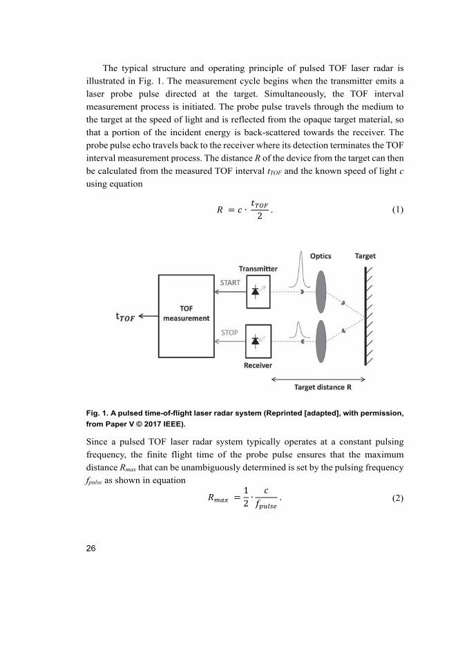
The typical structure and operating principle of pulsed TOF laser radar is
illustrated in Fig. 1. The measurement cycle begins when the transmitter emits a
laser probe pulse directed at the target. Simultaneously, the TOF interval
measurement process is initiated. The probe pulse travels through the medium to
the target at the speed of light and is reflected from the opaque target material, so
that a portion of the incident energy is back-scattered towards the receiver. The
probe pulse echo travels back to the receiver where its detection terminates the TOF
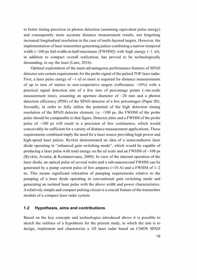
interval measurement process. The distance R of the device from the target can then
be calculated from the measured TOF interval tTOF and the known speed of light c
using equation
𝑅 𝑐 ∙
𝑡2
. (1)
Fig. 1. A pulsed time-of-flight laser radar system (Reprinted [adapted], with permission,
from Paper V © 2017 IEEE).
Since a pulsed TOF laser radar system typically operates at a constant pulsing
frequency, the finite flight time of the probe pulse ensures that the maximum
distance Rmax that can be unambiguously determined is set by the pulsing frequency
fpulse as shown in equation
𝑅 12∙
𝑐𝑓
. (2)
27
In other words, the probe pulse echo from the target has to reach the receiver prior
to the emission of the next probe pulse (Rieger, 2014). Since the pulsed TOF
distance measurement comes down to a time interval measurement between two
incidents, i.e. the emission of a probe signal and the detection of its echo from the
target, the accuracy of the distance measurement is dependent on the accuracy of
the temporal definition of these two incidents and of the measurement of the time
interval between the two.
The generation of the start signal for the TOF interval measurement process,
which must be properly synchronized with the instant of probe pulse emission, is
typically less of a problem and is not the main contributor to any inaccuracy of the
laser radar system. No matter whether an electrical or optical method is employed,
the pump current pulse and the optical probe pulse emission have relatively
predictable characteristics, thus rendering the generation of start signal timing mark
fairly straightforward. The actual problem lies in generating a stop signal that is
properly synchronized with the instant of echo detection. This is because the timing
of detection instant is affected by both variation in the amplitude of the echo signal
and noise present in the system (Bertolini, 1968).
The main function of the receiver is to detect the optical echo reflected from
the target and to generate a timely stop signal which terminates the process of TOF
measurement. In the ideal case the timing of the stop signal should be dependent
only on the target distance, so that it is fully insensitive to variation in the amplitude
of the optical signal and to the effect of noise. In reality, though, both do have an
effect on the timing of the stop signal generated by the receiver and therefore on
the precision and accuracy of the measurements. A variety of approaches regarding
the detectors and receiver channels have been proposed and implemented in order
to ensure accurate stop signal timing under widely fluctuating operating conditions.
Technically, these approaches are categorized as either linear detection or
single-photon detection techniques depending on the operation of the detector
(McManamon et al., 2017).
The following sections introduce these two techniques in sufficient depth for
the purposes of this work. The inclusion of linear detection techniques in this thesis
is aimed at conveying a general understanding of the performance and
implementation of conventional 1D laser radar techniques, and at providing a
context and motivation for the development of laser radar employing SPAD-based
single-photon detection rather than at making a comprehensive comparison
between the technologies. The section introducing single-photon detection will
serve as the theoretical and conceptual basis for the subsequent chapters concerning

28
the design and implementation of a single-photon detection-based laser radar
system. Before introducing the linear and single-photon detection techniques,
however, it is reasonable to consider some general matters regarding signals and
noise that are relevant to optical detection, and to mention a particular noise source
that is inherent to any optical signal, known as signal photon noise.
2.1 Signal and solar background noise
Due to the digital nature of a SPAD detector, i.e. the generation of a standard
response to individual detected photons, it is reasonable to consider the magnitude
of the received optical power in terms of the quantity of photons. The number of
photons can be used to estimate laser radar performance in terms of detection rate,
measurement distance vs. measurement time and SNR, for instance. The radar
equation (Collis & Russell, 1976) of
𝑛 𝐸 ∙𝜆ℎ ∙ 𝑐
∙𝐴
𝜋 ∙ 𝑅∙ 𝜏 ∙ 𝜖 (3)
provides a theoretical basis for estimating the number of photons, npho, incident on
the receiver aperture that are reflected from a diffuse (Lambertian) target at a
distance R. The other equation parameters are the total energy of the probe pulse,
Epulse [J], wavelength of the laser emission, λ [m], the Planck constant, h [m2 kg / s],
the speed of light, c [m/s], the area of receiver aperture, Ar [m2], the efficiency of
the optics, τ, and the target reflectivity, ϵ. The radar equation contains an inverse dependence of the received power on
the square of the distance. From this it follows that a variation of 1:100 in the
measured distance corresponds to a 1:10 000 variation in the received power,
assuming a single optical axis. Moreover, the reflectivity of the real-world diffuse
targets can vary within an order of magnitude or more. These two factors combined
will introduce a dynamic range of ~1:100 000 into the probe pulse echo within
which the receiver has to be able to discriminate the accurate timing for a stop
signal. Wide variations in input signal amplitude are problematic, since they
introduce an optical input signal amplitude-dependent systematic timing error,
known as walk error, which detracts from the accuracy of measurements (Gedcke
& Williams, 1968). More information on detection technique-dependent walk error
mechanisms and means of coping with this problem are presented in the sections
dealing with linear and single-photon detection techniques.

29
Any photons other than those from the probe pulse that reach the detector
represent a potential source of unwanted noise, detracting from receiver sensitivity
and the accuracy of the measurement result. These photons induce false detections,
which are particularly problematic in the case of single-photon detection techniques,
since they potentially mask the signal photons from detection and in the worst case
can cause total detector blocking, i.e. a complete loss of signal (Fouche, 2003;
Henriksson, 2005; Kostamovaara, Jahromi, & Keränen, 2020). Background
photons may arrive at the detector either from a radiating source or via reflecting
elements residing within the field of view of the detector. Radiating sources of
background photons may be both natural and artificial. One example of a well-
known natural source of background photons is the Sun, which can potentially
cause particularly high-level background radiation affecting outdoor laser radar
applications.
The total power of the solar background radiation PBG received by a single
SPAD detector element can be estimated by means of equation (Paper III)
𝑃 𝐼 ∙ 𝐴 ∙ 𝜌 ∙ 𝐹𝑂𝑉
2∙ 𝐵𝑊 (4)
in which the parameters are area of the receiver aperture, Ar [m2], the target
reflectivity, ρtarget, the linear field of view of a single SPAD detector element,
FOVSPAD (~Φdet / foptics) [rad], the optical bandwidth of the receiver, BWopt [Å], and
the solar spectral irradiance, IS [W / m2 Å]. Equation (4) further assumes a diffuse
i.e. Lambertian target. As is apparent from equation (4), the ways to reduce the total
background power, and thus the detrimental effects of background radiation
(masking and blocking), are spatial and spectral filtering. Of the two, reduction of
the FOV of the detector is particularly effective due to its squared effect, whereas
effective spectral filtering requires the use of narrow optical band pass filters.
The mean time Tmean pho between photons in the background photon flux at
given background radiation power levels and photon wavelengths can be estimated
by equation
𝑇 𝐸𝑃
ℎ ∙ 𝑐𝜆
∙1𝑃
. (5)
This photon mean time can then be converted in equation
30
𝑇
1PDE
∙ 𝑇 (6)
to the mean time between background photon detections, Tmean det, by reference to
photon detection efficiency (PDE) of the detector element (see chapter 2.4.1). The
probability of background photons inducing detection pdet within the time interval
(i.e. detection window) ΔT, is presented in equation
𝑝 1 𝑒∆
. (7)
This probability function is a consequence of the Poisson distribution of the
background photon flux (see chapter 2.2) and is used to estimate the magnitude of
background photon-induced masking and blocking effects in a system in which the
detector is capable of a single detection per probe pulse at the most. For small
argument values (<0.1) the probability of background photon detection is
~ΔT/Tmean det. Equation
SN R 𝑒∙ ∙
∙𝑛 ∙ PDE ∙ 𝑁
𝑡𝑇
(8)
provides an estimated signal-to-noise ratio SNBGR, defined here as the ratio of the
number of signal detections to the square root of the number of background photon
detections during signal (Kostamovaara et al., 2020). The equation (8) ignores the
effect of signal photon shot noise and hence does not represent the total SNR.
Equation (8) does, however, provide a fairly valid estimate for the total SNR when
background detection-related noise predominates, which is often the case at the
limit of signal detection in practical measurement settings. The terms Nmeas and tpulse
are the number of measurement cycles and the width of the probe pulse,
respectively. The first square root term in the numerator represents the blocking
effect due to the background photon detections accounting for an exponential decay
in the SNR as a function of the power of the background radiation and the detection
efficiency. The term in the denominator represents noise related to the number of
background photon detections during the signal. What is also notable in the latter
term is that it provides a justification for the employment of a narrow probe pulse,
since it reduces the number of background photon detections during the signal, and
therefore improves the SNR.
31
2.2 Photon shot noise and photon statistics
The inverse relation between the energy of a photon and its wavelength implies that
as the wavelength of electromagnetic radiation decreases the energy of the photons
increases (Grum & Becherer, 1979, p. 91). Detection of individual optical photons
is possible since they have sufficient energy to cause detectable phenomena in the
electrical properties of the photodetector element. The effects of individual
significantly less energetic microwave photons, on the other hand, are
indistinguishable on account of thermal and other noise (Heinzen & Wineland,
1990). In addition, assuming that the power of the electromagnetic radiation is
constant, the number of photons per unit time will decrease along with the
wavelength, rendering the stream of photons increasingly grainy, as it were, and the
quantum nature of the electromagnetic radiation increasingly apparent.
Photon shot noise is a form of noise inherent to any optical signal and is
manifested as a statistical distribution of the quantity of photons occurring within
a specific time interval (i.e. detection time window). The probability P(n) of the
occurrence of a certain number of photons n has a Poisson distribution and is
expressed by equation
𝑃 𝑛𝑛𝑛!
𝑒 , (9)
in which n̂ is the mean number of photons (Grum & Becherer, 1979, p. 93). An
example of the probabilities of a number of photons occurring in the photon flux
given three different mean numbers of photons is presented in Fig. 2. At a mean
number of photons n̂ = 0.1 or less, the probability of the occurrence of two or more
photons is negligible, thus virtually any photon occurrence is due to a single photon.
At higher values of the mean number of photons, however, the probabilities of the
occurrence of multiple photons also increase.
One characteristic feature of a nonlinear single-photon detector is that it
outputs a standard digital-like response irrespective of the magnitude of the photon
stimulus. It should be noted, however, that the actual timing of the response
depends on this fact (Blazej & Prochazka, 2009). In single-photon detection mode,
the photon events are caused by a single photon, so that the avalanche breakdown
events are identical, resulting in a standard TOF distribution. In this mode the
photon detection response is free from timing variation that is dependent on the
magnitude of the optical stimulus, i.e. walk error (more on walk error in a SPAD
detector, see chapter 2.4.2). In single-photon detection mode there is also a linear
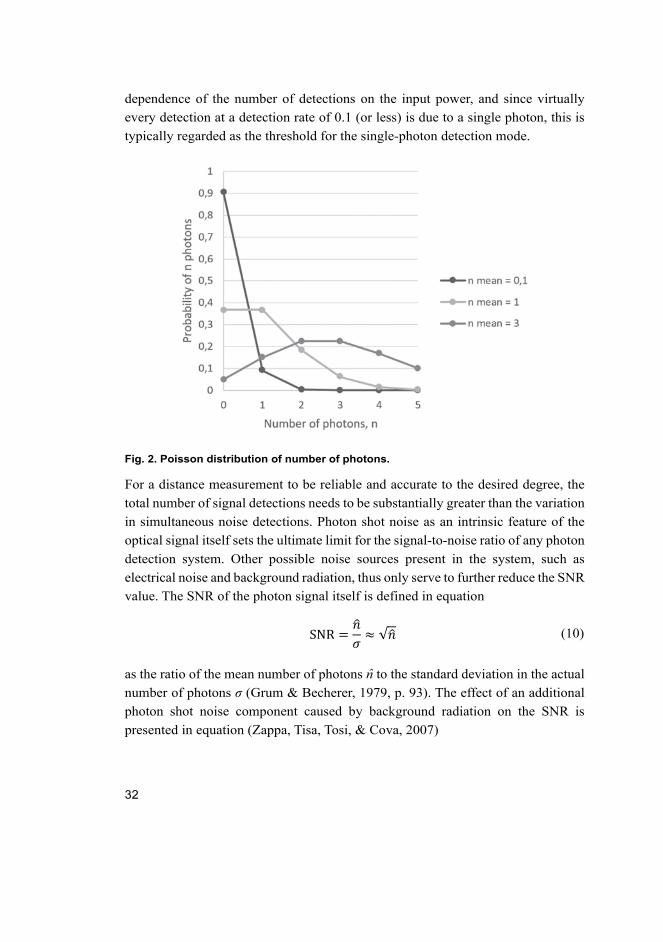
32
dependence of the number of detections on the input power, and since virtually
every detection at a detection rate of 0.1 (or less) is due to a single photon, this is
typically regarded as the threshold for the single-photon detection mode.
Fig. 2. Poisson distribution of number of photons.
For a distance measurement to be reliable and accurate to the desired degree, the
total number of signal detections needs to be substantially greater than the variation
in simultaneous noise detections. Photon shot noise as an intrinsic feature of the
optical signal itself sets the ultimate limit for the signal-to-noise ratio of any photon
detection system. Other possible noise sources present in the system, such as
electrical noise and background radiation, thus only serve to further reduce the SNR
value. The SNR of the photon signal itself is defined in equation
SNR𝑛𝜎
√𝑛 (10)
as the ratio of the mean number of photons n̂ to the standard deviation in the actual
number of photons σ (Grum & Becherer, 1979, p. 93). The effect of an additional
photon shot noise component caused by background radiation on the SNR is
presented in equation (Zappa, Tisa, Tosi, & Cova, 2007)
33
SNR
𝑛𝜎 𝜎
𝑛
𝑛 𝑛 . (11)
The significance of photon shot noise for the whole laser radar system varies
depending on the detection technique employed. In a linear detection receiver with
an APD detector the electrical noise of the receiver is typically the dominant noise
source, thus setting the limits for the sensitivity and precision of the system. In
single-photon detection, on the other hand, photon shot noise becomes more
important, since in the case of a low background noise level it is this that is the
dominant noise source.
2.3 Linear detection techniques
Linear detection techniques imply that the optical detection itself operates in a
linear manner, i.e. the electrical response of the detector is linearly proportional to
the optical input signal. Several schemes have been developed for time
discrimination in linear detection, such as leading-edge timing discriminator,
Constant Fraction Discriminator (CFD) and zero crossing timing (Amann et al.,
2001). Leading-edge timing discriminator, which is probably the simplest of the
above schemes, is used here as an example and will serve as a reference for linear
detection techniques later in this chapter. Besides the simplicity of the technique,
leading-edge timing discriminator also has the advantage that timing discrimination
takes place at the rising edge of the signal, i.e. before any saturation of the receiver
channel can occur. This means that a high dynamic range in the input signal will
not suffer from strict linearity requirement for accurate operation, as is the case
with linear timing discrimination schemes (Nissinen, 2011). This section presents
the central ideas related to a conventional laser radar operating in the linear
detection mode, its system requirements and typical performance parameters.
Moreover, section 2.3.1 presents considerations regarding error sources
characteristic of linear detection, including input signal amplitude-dependent walk
error and forms of noise and their effects.
The implementation of pulsed TOF laser radars has traditionally been based on
use of an avalanche photo diode (APD) detector in conjunction with an analogue
receiver channel. An APD detector is a discrete semiconductor element that
requires a reverse bias of ~200V, for example (thick Si APD), to achieve improved
photon sensitivity through photocurrent amplification. The function of the receiver
channel is to convert and amplify the photocurrent signal from the APD to a suitable
34
voltage for further signal processing and eventual timing discrimination of the stop
signal. In order to perform the above functions with sufficient accuracy and within
a given high dynamic range of the probe pulse echo in the presence of noise, the
receiver channel has to meet demanding specifications (high gain, wide bandwidth,
low noise) (Muoi, 1984), which renders the design of a linear receiver channel
anything but a trivial task and its implementation consuming in terms of IC area.
The power requirement for a probe pulse in a pulsed TOF laser radar aiming at
non-cooperative targets in a distance range of several tens of metres, is a few tens
of watts, assuming reasonable-sized optics of a few tens of millimetres in diameter.
The peak value of the drive current pulse required for generating the above laser
pulse with an appropriate laser diode is ~20 A or more. Conventionally, an
avalanche transistor has been used as the high-speed switch employed in an RLC
discharge-type current pulser, thus setting the minimum width of the current pulse,
and also that of the laser pulse itself, in the range 3–5 ns. One significant drawback
when employing an avalanche transistor, however, is that the maximum pulsing
frequency is only a few tens of kilohertz, being limited by resistive heating caused
by large residual voltage over the device (Vainshtein, Yuferev, & Kostamovaara,
2003).
2.3.1 Timing walk error and the effect of noise on linear detection
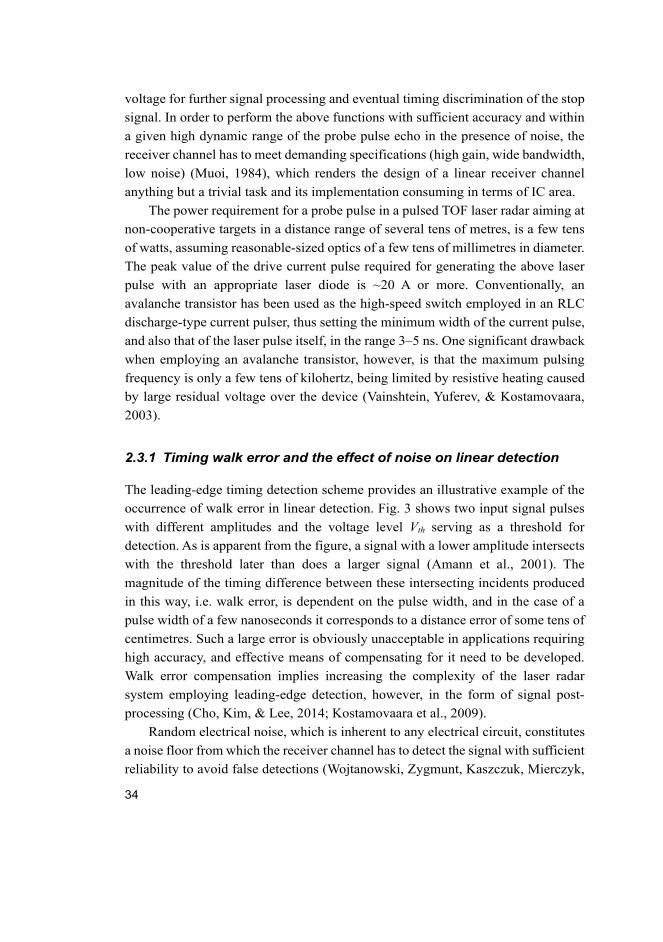
The leading-edge timing detection scheme provides an illustrative example of the
occurrence of walk error in linear detection. Fig. 3 shows two input signal pulses
with different amplitudes and the voltage level Vth serving as a threshold for
detection. As is apparent from the figure, a signal with a lower amplitude intersects
with the threshold later than does a larger signal (Amann et al., 2001). The
magnitude of the timing difference between these intersecting incidents produced
in this way, i.e. walk error, is dependent on the pulse width, and in the case of a
pulse width of a few nanoseconds it corresponds to a distance error of some tens of
centimetres. Such a large error is obviously unacceptable in applications requiring
high accuracy, and effective means of compensating for it need to be developed.
Walk error compensation implies increasing the complexity of the laser radar
system employing leading-edge detection, however, in the form of signal post-
processing (Cho, Kim, & Lee, 2014; Kostamovaara et al., 2009).
Random electrical noise, which is inherent to any electrical circuit, constitutes
a noise floor from which the receiver channel has to detect the signal with sufficient
reliability to avoid false detections (Wojtanowski, Zygmunt, Kaszczuk, Mierczyk,
35
& Muzal, 2014). In leading-edge detection, this reliability is acquired by raising
the detection threshold level above the noise floor by an amount corresponding to
a sufficient SNR at the detection instant. Insensitivity to false detections thus comes
at the price of decreased signal photon sensitivity. The actual SNR values are
application-specific, of course, but typical SNR figures for laser radar applications
are in the range of 5–10 when providing a sufficiently low probability of false
detection (Wojtanowski et al., 2014).
Fig. 3. Walk error in the leading-edge detection technique (geometrical part).
The following examples estimate the number of individual photons required for
reliable detection of a probe pulse echo and the transmitted pulse power required
for reliable detection from a target at a certain distance. The estimates rely on
typical system parameters for a linear detection receiver employing leading-edge
threshold detection. The receiver bandwidth of 200 MHz, sufficient for tracking an
input signal with a rise time of about a nanosecond, and the input-referred noise
current of 5 pA / √Hz typical of a modern receiver channel would result in a total
electrical input noise of 70 nArms while an SNR value of 10 at the detection instant
would result in a signal current of ~1 µA, whereupon, with an APD detector
responsivity of 30 A/W, the input signal power required for reliable detection would
be 30 nW. This power corresponds to approximately 400–500 photons in the NIR
wavelength region. As for the question of sufficient transmitted power, assuming
that the diameter of the receiver aperture is 18 mm and the target distance 50 m,
with a reflectivity of 8%, it would follow that the minimum power of the probe
pulse required for reliable echo detection would be 15 W (total pulse energy 45 nJ,
3 ns FWHM) (Paper III).
36
Noise is also a source of inaccuracy that can determine the single-shot precision
of a linear detection receiver. Based on the above estimate of the total electrical
noise and the given probe pulse characteristics and SNR at the detection instant,
the single-shot precision of the laser radar system would be trise/SNR ~ 150 ps
(22 mm, σ-value) (Kurtti, 2012).
The final consideration regarding the performance of linear detection
techniques is the effect of background radiation on the detection sensitivity of
signal photons and on the precision of the resulting measurements. As with signal
photons, background photons also induce a photocurrent that has a noise
component proportional to its amplitude, thus increasing the total noise level of the
receiver. The effect of background photon-induced noise is qualitatively equal to
that of electrical noise in that it will increase the total RMS noise of the receiver
and thus reduce its sensitivity and the precision of the measurement. Even though
the photon sensitivity will be reduced by background radiation, total blocking of
the detector will not in principle occur because of it. This feature is justifiably a
significant advantage of linear detection over single-photon detection.
2.4 The SPAD technique
This section will be concerned with a single-photon detection technique in which
the stop signal timing is based on the time-correlated detection of individual
photons within the envelope of a probe pulse echo. Such an extreme photon
sensitivity is a highly desirable feature of a laser radar system, since such systems
often operate under photon-starved conditions and the magnitude of the echo signal
may be very weak, i.e. down to a single photon or less per probe pulse. The photon
sensitivity of a single-photon detector results from the high photocurrent gain in
the device, i.e. the gain is virtually infinite due to device breakdown (Zappa et al.,
2007). Other desirable characteristics of a single-photon detector are small
temporal jitter between photon absorption and the output signal and a digital-like
output signal (Cova et al., 1996), which would eliminate the need for a complex
receiver channel and be insensitive to EMI. High photon sensitivity and an
uncomplicated output signal induced by absorption of a single photon that is readily
converted to a logic-level signal would render the single-photon detection
technique a viable alternative for a laser radar detector.
The conventional method for detecting individual photons is based on the use
of a photomultiplier tube (PMT). PMTs have several desirable performance
features with respect to single-photon detection, including high photon sensitivity
37
and quantum efficiency, and low noise and timing jitter in photon detection, but
their physical construction, i.e. a sizable vacuum tube, places serious limits on their
applicability. High performance PMT implementations are costly, bulky and fragile,
and their operation requires supply voltages in the kilovolt range. These reasons
make their use in laser radars, particularly miniature-sized ones employing detector
arrays, virtually impossible (Zappa et al., 2007).
A more recent alternative for single-photon detection is a semiconductor device
known as a single-photon avalanche diode (SPAD). As a CMOS-compatible
semiconductor device, a SPAD has several desirable characteristics, including a
compact, robust physical structure, high performance and efficiency, and low cost.
Consequently, these SPAD detector techniques have been objects of
ever-increasing research and development interest recently, opening the possibility
of constructing an optical receiver module possessing a high level of integration
and achieving excellent performance.
2.4.1 Basics of a SPAD detector
A SPAD element employed as a single-photon detector is a p-n junction biased
above its breakdown voltage. A strong electric field established within the depletion
region accelerates free carriers, i.e. electron hole pairs (EHP), and provides them
with sufficient kinetic energy to generate secondary carriers by an impact ionization
mechanism. Impact ionization results in a rapidly accumulating avalanche
multiplication of charge carriers within the depletion region, which is observed as
a self-sustaining milliampere-scale current passing through the junction (Cova et
al., 1996). This SPAD detector is a type of nonlinear detector, since in principle it
generates a standard output response irrespective of the magnitude of the photon
stimulus.
Such a large-scale current signal is readily converted to a logic-level stop signal
with a simple electric circuit, thus significantly simplifying the design of the
receiver electronics, in contrast to the linear detection receiver channel. What is
more, the avalanche built-up process is a particularly fast phenomenon, thus
providing accurate temporal information about the actual event of EHP generation,
i.e. photon absorption timing (Cova et al., 1996). The jitter between the photon
absorption event and the resulting output signal from a modern high-speed CMOS
Si SPAD element is <100 ps corresponding to a distance precision of less than
15 mm (Zappa et al., 2007). High photon sensitivity down to a single photon and a
logic-level output signal with high timing precision are the key characteristics

38
behind the use of a SPAD detector for pulsed TOF laser radar purposes, and the
same characteristics mean that a SPAD detector can be rightly regarded as a “digital”
photodetector (Cova, Longoni, & Andreoni, 1981).
Even though silicon SPAD detector has high photon sensitivity, this is not a
sufficient description of its potential as a photon detector. Photon detection by
means of a SPAD detector is a probabilistic and photon wavelength-dependent
process. That is to say, a SPAD detector is capable of detecting individual photons
impinging on it, but not every one of them. This feature, known as photon detection
efficiency (PDE), represents a non-ideal characteristic of SPAD detectors. For
example, the PDE of a silicon SPAD detector operating at near-infrared (NIR)
wavelengths is only a few percent (Tosi et al., 2014), which implies that a few tens
of photons on average are required for an actual detection, which is still about one
order of magnitude fewer than the threshold of reliable detection for an APD
detector with a linear receiver channel (Paper III). As for the maximum available
detection rate of a SPAD detector, the avalanche surge, once initiated, needs to be
quenched before subsequent photon detection by lowering the bias voltage below
the breakdown voltage. This process induces a finite time interval, known as “dead
time”, during which the detector is unable to detect any photons, a situation that
affects the maximum detection rate. Typical dead times for CMOS SPADs are
around 10–20 ns, resulting in a theoretical maximum detection rate of ~100 MHz.
2.4.2 Walk error and false detections
The accuracy of a SPAD detector may suffer from a systematic optical input signal
amplitude-dependent walk error that arises from the fact that the avalanche build-up
speed depends on the number of primary carriers (Blazej & Prochazka, 2009).
Unlike the situation in the actual single-photon mode, in which avalanche incidents
are considered “identical”, as they result from a single primary carrier, the
dynamics of the avalanche response in multi photon mode depends on the number
of primary carriers. The greater the magnitude of the optical stimulus, the more
primary carriers are generated resulting in faster avalanche build-up. This advances
the TOF distribution of the target, causing it to appear to be closer than it actually
is. This walk error occurs when the input signal power is increased, e.g. under
conditions where the target is at close range or has high reflectance and potentially
introduces a cm-scale error into the distance measurement. In single-photon mode,
however, the distance measurement results are free of walk error.
39
In addition, the finite rise time and width of the probe laser pulse may induce
walk error. Due to its high photon sensitivity and given an optical input of sufficient
magnitude, a SPAD detector will tend to trigger due to photons in the front part of
the optical pulse, i.e. earlier photons in the probe pulse envelope emitted before the
actual lasing. In this case the magnitude of the walk error is dependent on the power
distribution and the width of the leading-edge of laser pulse.
Any triggering except that from the probe pulse echo must be regarded as false
detection i.e. noise. False detections are harmful since they may mask detections
caused by signal photons. The primary carrier, i.e. the original free carrier required
to initiate the avalanche multiplication process, may be either thermally generated
or brought about by the absorption of any incident photon with sufficient ionization
energy. Triggerings caused by thermally generated carriers, also known as “dark
counts”, are a source of noise produced by the SPAD detector itself, but the dark
count rate (DCR) of a modern CMOS SPAD (diameter <50 µm) is typically not a
major issue due to the much greater contribution of background radiation (Pancheri
& Stoppa, 2007).
Photon induced EHPs originate either from appropriate probe signal echo
photons or else from unwanted false detections caused by background radiation
photons. When employing the single-photon detection technique, background
photon noise may become a serious problem, particularly in outdoor applications
aiming at making long-distance measurements. High-level background radiation
will reduce the signal detection rate and thus increase the measurement time, and
in the worst case and with certain types of receiver configuration (giving only one
measurement for an emitted laser pulse), may block the detector altogether from
signal photons that are to be detected. There are three methods available for
reducing the effect of background radiation: temporal, spatial and spectral filtering
(Pfennigbauer & Ullrich, 2007).
2.4.3 Silicon photomultiplier
It is worth mentioning that although the SPAD detector is insensitive to the
amplitude of the photon stimulus due to its nonlinear nature, there is a way to
circumvent this limitation to certain extent by employing a detector containing
multiple SPAD elements. During the recent years, several IC manufacturers
(Broadcom, ON Semiconductor, Hamamatsu etc.) have introduced a variety of
silicon photomultiplier (SiPM) detectors, often regarded as a viable solid-state
alternative for the PMTs. SiPM detectors contain an array of SPAD elements,

40
enabling a single-photon detection timing with high precision, but also information
on the number of detected photons. SiPM detectors operating in both analogue and
digital manner have been implemented and studied.
An analogue SiPM detector contains a large array (hundreds, thousands) of
detector pixels (including a SPAD detector element with a series quench resistor)
that are parallel connected to a common electrode. Therefore, the amplitude of the
analogue output signal of the SiPM detector is proportional to the number of
triggered pixels, and in the case of triggerings due to photon detections, to the
number of detected photons (Renker, 2006). The employment of analogue SiPM
detector involves the general issues associated with analogue signal processing that
are complex and sensitive circuits and performance degradation due to noise, for
example. Evidently the number of pixels sets the ultimate limit to the dynamic
range of the SiPM detector employed in photon counting and due to the common
output signal the detection timing of individual detector pixels is not possible.
With digital SiPMs it is possible to further exploit the advantageous intrinsic
performance features of the SPAD detector (<100 ps timing precision, moderate
PDE, maximal counting rate etc.) (Cova et al., 1996). In contrast to its analogue
counterpart, the digital SiPM employs active quenching and has individual TDC
per each SPAD element enabling the measurements of the number of photons and
the SPAD-wise photon detection timing. As the term suggests the digital SiPM has
a discrete output signal, therefore simplifying the receiver electronics and signal
processing. For more on descriptions and comparison of analogue and digital
SiPMs, see (Frach et al., 2009).
2.5 Single-photon detection and statistical sampling
From a distance measurement point of view, any triggering of a SPAD detector
resulting from forms of excitation other than absorption of the photons of a probe
pulse echo must be considered false detections, i.e. noise. In the presence of false
detections primarily caused by photons belonging to background radiation or dark
counts, which in both cases are random in nature, measurements based on a single
detection will ultimately be unreliable. This is an essential difference relative to
linear detection, in which every probe pulse echo from the target is detected
(implying that signal detection is possible with the transient recording approach
even at SNR <1, by averaging). For this reason, single-photon detection is usually
employed in the statistical sampling mode, in which a quantity of independent TOF
measurements are first accumulated into a histogram, which is then processed and
41
analysed to distinguish the signal from the noise and thus obtain the distance from
the target (Wallace, Buller, & Walker, 2001).
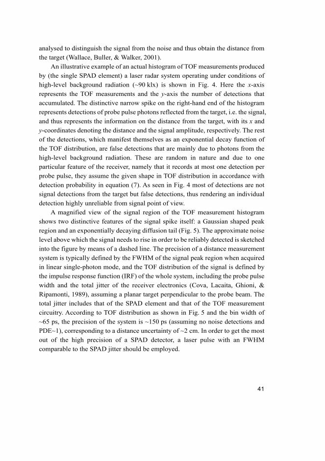
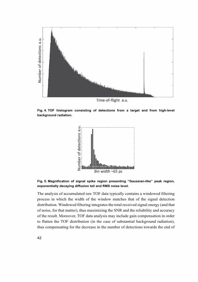
An illustrative example of an actual histogram of TOF measurements produced
by (the single SPAD element) a laser radar system operating under conditions of
high-level background radiation (~90 klx) is shown in Fig. 4. Here the x-axis
represents the TOF measurements and the y-axis the number of detections that
accumulated. The distinctive narrow spike on the right-hand end of the histogram
represents detections of probe pulse photons reflected from the target, i.e. the signal,
and thus represents the information on the distance from the target, with its x and
y-coordinates denoting the distance and the signal amplitude, respectively. The rest
of the detections, which manifest themselves as an exponential decay function of
the TOF distribution, are false detections that are mainly due to photons from the
high-level background radiation. These are random in nature and due to one
particular feature of the receiver, namely that it records at most one detection per
probe pulse, they assume the given shape in TOF distribution in accordance with
detection probability in equation (7). As seen in Fig. 4 most of detections are not
signal detections from the target but false detections, thus rendering an individual
detection highly unreliable from signal point of view.
A magnified view of the signal region of the TOF measurement histogram
shows two distinctive features of the signal spike itself: a Gaussian shaped peak
region and an exponentially decaying diffusion tail (Fig. 5). The approximate noise
level above which the signal needs to rise in order to be reliably detected is sketched
into the figure by means of a dashed line. The precision of a distance measurement
system is typically defined by the FWHM of the signal peak region when acquired
in linear single-photon mode, and the TOF distribution of the signal is defined by
the impulse response function (IRF) of the whole system, including the probe pulse
width and the total jitter of the receiver electronics (Cova, Lacaita, Ghioni, &
Ripamonti, 1989), assuming a planar target perpendicular to the probe beam. The
total jitter includes that of the SPAD element and that of the TOF measurement
circuitry. According to TOF distribution as shown in Fig. 5 and the bin width of
~65 ps, the precision of the system is ~150 ps (assuming no noise detections and
PDE~1), corresponding to a distance uncertainty of ~2 cm. In order to get the most
out of the high precision of a SPAD detector, a laser pulse with an FWHM
comparable to the SPAD jitter should be employed.
42
Fig. 4. TOF histogram consisting of detections from a target and from high-level
background radiation.
Fig. 5. Magnification of signal spike region presenting “Gaussian-like” peak region,
exponentially decaying diffusion tail and RMS noise level.
The analysis of accumulated raw TOF data typically contains a windowed filtering
process in which the width of the window matches that of the signal detection
distribution. Windowed filtering integrates the total received signal energy (and that
of noise, for that matter), thus maximizing the SNR and the reliability and accuracy
of the result. Moreover, TOF data analysis may include gain compensation in order
to flatten the TOF distribution (in the case of substantial background radiation),
thus compensating for the decrease in the number of detections towards the end of
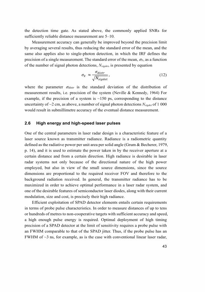
43
the detection time gate. As stated above, the commonly applied SNRs for
sufficiently reliable distance measurement are 5–10.
Measurement accuracy can generally be improved beyond the precision limit
by averaging several results, thus reducing the standard error of the mean, and the
same also applies also to single-photon detection, in which the IRF defines the
precision of a single measurement. The standard error of the mean, σx̅ , as a function
of the number of signal photon detections, Nsigdet, is presented by equation
𝜎
𝜎
𝑁 , (12)
where the parameter σdistr is the standard deviation of the distribution of
measurement results, i.e. precision of the system (Neville & Kennedy, 1964) For
example, if the precision of a system is ~150 ps, corresponding to the distance
uncertainty of ~2 cm, as above, a number of signal photon detections Nsigdet of 1 000
would result in submillimetre accuracy of the eventual distance measurement.
2.6 High energy and high-speed laser pulses
One of the central parameters in laser radar design is a characteristic feature of a
laser source known as transmitter radiance. Radiance is a radiometric quantity
defined as the radiative power per unit area per solid angle (Grum & Becherer, 1979,
p. 14), and it is used to estimate the power taken in by the receiver aperture at a
certain distance and from a certain direction. High radiance is desirable in laser
radar systems not only because of the directional nature of the high power
employed, but also in view of the small source dimensions, since the source
dimensions are proportional to the required receiver FOV and therefore to the
background radiation received. In general, the transmitter radiance has to be
maximized in order to achieve optimal performance in a laser radar system, and
one of the desirable features of semiconductor laser diodes, along with their current
modulation, size and cost, is precisely their high radiance.
Efficient exploitation of SPAD detector elements entails certain requirements
in terms of probe pulse characteristics. In order to measure distances of up to tens
or hundreds of metres to non-cooperative targets with sufficient accuracy and speed,
a high enough pulse energy is required. Optimal deployment of high timing
precision of a SPAD detector at the limit of sensitivity requires a probe pulse with
an FWHM comparable to that of the SPAD jitter. Thus, if the probe pulse has an
FWHM of ~3 ns, for example, as is the case with conventional linear laser radar,
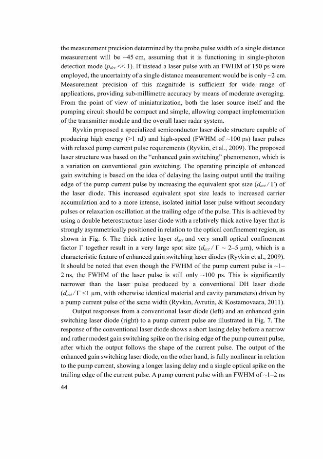
44
the measurement precision determined by the probe pulse width of a single distance
measurement will be ~45 cm, assuming that it is functioning in single-photon
detection mode (pdet << 1). If instead a laser pulse with an FWHM of 150 ps were
employed, the uncertainty of a single distance measurement would be is only ~2 cm.
Measurement precision of this magnitude is sufficient for wide range of
applications, providing sub-millimetre accuracy by means of moderate averaging.
From the point of view of miniaturization, both the laser source itself and the
pumping circuit should be compact and simple, allowing compact implementation
of the transmitter module and the overall laser radar system.
Ryvkin proposed a specialized semiconductor laser diode structure capable of
producing high energy (>1 nJ) and high-speed (FWHM of ~100 ps) laser pulses
with relaxed pump current pulse requirements (Ryvkin, et al., 2009). The proposed
laser structure was based on the “enhanced gain switching” phenomenon, which is
a variation on conventional gain switching. The operating principle of enhanced
gain switching is based on the idea of delaying the lasing output until the trailing
edge of the pump current pulse by increasing the equivalent spot size (dact / Γ) of
the laser diode. This increased equivalent spot size leads to increased carrier
accumulation and to a more intense, isolated initial laser pulse without secondary
pulses or relaxation oscillation at the trailing edge of the pulse. This is achieved by
using a double heterostructure laser diode with a relatively thick active layer that is
strongly asymmetrically positioned in relation to the optical confinement region, as
shown in Fig. 6. The thick active layer dact and very small optical confinement
factor Γ together result in a very large spot size (dact / Γ ~ 2–5 µm), which is a
characteristic feature of enhanced gain switching laser diodes (Ryvkin et al., 2009).
It should be noted that even though the FWHM of the pump current pulse is ~1–
2 ns, the FWHM of the laser pulse is still only ~100 ps. This is significantly
narrower than the laser pulse produced by a conventional DH laser diode
(dact / Γ <1 µm, with otherwise identical material and cavity parameters) driven by
a pump current pulse of the same width (Ryvkin, Avrutin, & Kostamovaara, 2011).
Output responses from a conventional laser diode (left) and an enhanced gain
switching laser diode (right) to a pump current pulse are illustrated in Fig. 7. The
response of the conventional laser diode shows a short lasing delay before a narrow
and rather modest gain switching spike on the rising edge of the pump current pulse,
after which the output follows the shape of the current pulse. The output of the
enhanced gain switching laser diode, on the other hand, is fully nonlinear in relation
to the pump current, showing a longer lasing delay and a single optical spike on the
trailing edge of the current pulse. A pump current pulse with an FWHM of ~1–2 ns
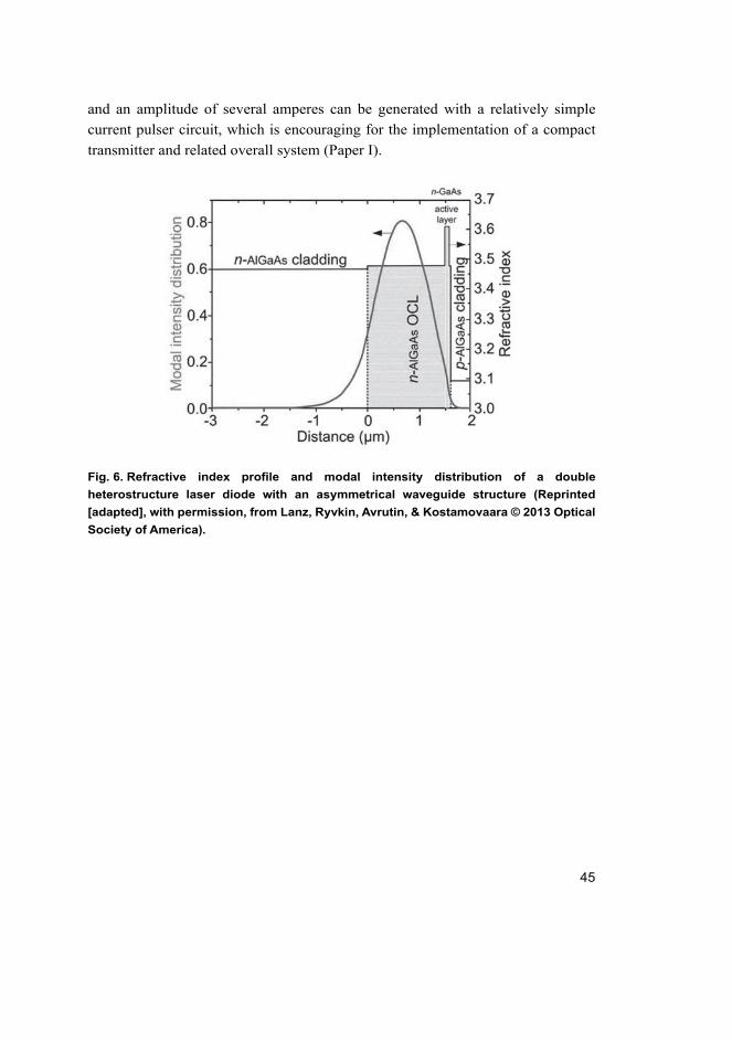
45
and an amplitude of several amperes can be generated with a relatively simple
current pulser circuit, which is encouraging for the implementation of a compact
transmitter and related overall system (Paper I).
Fig. 6. Refractive index profile and modal intensity distribution of a double
heterostructure laser diode with an asymmetrical waveguide structure (Reprinted
[adapted], with permission, from Lanz, Ryvkin, Avrutin, & Kostamovaara © 2013 Optical
Society of America).
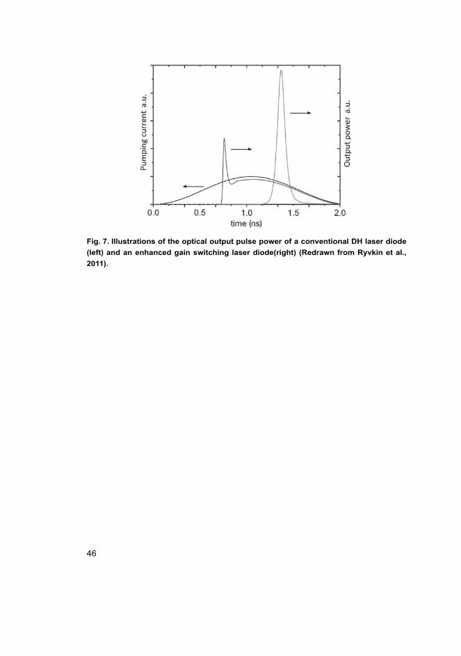
46
Fig. 7. Illustrations of the optical output pulse power of a conventional DH laser diode
(left) and an enhanced gain switching laser diode(right) (Redrawn from Ryvkin et al.,
2011).
47
3 Literature review
The aim of this literature review is to outline some developments in research into
laser radar techniques based on single-photon detection that are considered relevant
from the point of view of the present work. In order to confine the focus of this
review, given the large number of papers related to single-photon detection-based
laser radars, the approach will be further limited to cover mainly HW developments
in transmitter and receiver modules and complete laser radar systems. In addition,
some recent developments in linear detection techniques will be considered. The
basis of the approach adopted when evaluating the modules and laser radar systems
will not be restricted to performance but will also include feasibility, since the
development of practical technological solutions also lies at the core of the
engineering sciences.
Single-photon detection
In recent times there has been an ever-increasing interest in laser radar applications
employing single-photon detection technologies, and the focus appears to be on 3D
imager applications, due to their expected wide commercial potential and the need
for them in environment perception systems. One prominent current example of a
field interested in 3D imaging is the automobile industry.
Research into laser radars employing single-photon detection technologies has
consisted of circuit and system development activities mainly focusing on receiver
architectures constructed from large, dense CMOS SPAD detector arrays (Bronzi
et al., 2014; Niclass, Rochas, Besse, & Charbon, 2005; Zhang et al., 2019). By
contrast, research and development in the field of transmitter technologies for
optimizing probe pulses for use with SPAD detectors has with a few exceptions
been rare. This lack of research seems to have applied particularly where compact
SPAD-optimized transmitter implementations encouraging system integration are
concerned. A variety of application-specific 2D and 3D imager systems have been
developed and put forward, but only a very few of them could be regarded as
miniaturized solid-state imagers (Jahromi, 2020; Keränen & Kostamovaara, 2019).
Following the comprehensive studies on SPAD technology and its applicability
to laser radar systems (Massa et al., 1998; Pellegrini, Buller, Smith, Wallace, &
Cova, 2000), research related to distance measurement employing single-photon
detection has been active and a variety of detection technologies have been
presented, characterized and applied to for 1D distance measurements and
48
variations on this theme. Nevertheless, it appears that research focused on the
system integration of 1D laser radar has virtually been at a stand-still.
McCarthy proposed a long-range 3D scanner based on 1D distance
measurement employing a single Si SPAD detector element (McCarthy et al., 2009).
The system employed low energy optical pulses (a few tens of pJ) with a
pulse-width of ~90 ps and a pulsing rate of up to several tens of MHz, resulting in
an illumination with an average optical power of <50 µW. The emission wavelength
of the semiconductor laser diode was 842 nm, and the system was capable of
achieving a centimetre-scale xyz resolution up to a range of 325 m with a pixel
dwell time of one second. The fibre-coupled Si SPAD detector, pulsed laser diode
and data acquisition system were all commercially available modules. Distinctive
features of the quite complex optical design of the proposed system were a bulky
SLR camera lens with large aperture (72 mm) as the objective and a single-mode
fibre as a spatial filter to combat background radiation at the receiver.
For proof-of-concept purposes, test measurements were performed on a laser
radar system employing an individual custom-made Si SPAD detector and a bulk
laser diode operating in enhanced gain switching mode (Paper I). The transmitter
emitted laser pulses at 870 nm with a total pulse energy of ~1 nJ and an and FWHM
of ~100 ps, and it was capable of pulsing rates >100 kHz. The system demonstrated
centimetre-scale precision and a high measurement rate when resolving the planes
of a step-like 51 mm target at a distance of 50 m in 5 ms under conditions of high-
level background irradiation (70 klx). The system realization was a laboratory
construction lacking any substantial system integration aspect.
By comparison with the above systems employing laser transmitters emitting
at probe pulse wavelengths of ~850 nm, wavelengths longer than 1 µm are
advantageous for laser radar applications, since they undergo lower atmospheric
loss (Wojtanowski et al., 2014), they are exposed to reduced solar background
radiation and they are subject to less stringent eye safety restrictions (Forrester &
Hulme, 1981). One distinctive feature of receivers operating at these wavelengths
is that the detector materials are something other than Si, due to its insignificant
PDE in that region. Buller proposed a 3D scanner employing a superconducting
nanowire single-photon detector (SNSPD) and a mode-locked fibre laser emitting
at 1560 nm (Buller et al., 2012). The width of the laser pulse was <1 ps, the average
transmitted power <250 µW and the maximum pulsing rate 50 MHz. The maximum
reported measurement range was 4.4 km, with a precision of ~1.5 mm and a dwell
time per pixel of two seconds. The system implementation was a complex
laboratory setup composed of high-specification commercial off-the-shelf optical
49
telecommunication components. One distinctive feature of the system was that the
SNSPD detector was cooled to a temperature of 4 K in order to reduce its dark
count rate.
In another study, McCarthy proposed a 3D scanner likewise based on TOF
single-photon detection, but employing an individual InGaAs/InP semiconductor
SPAD detector and a pulsed supercontinuum laser transmitter (McCarthy et al.,
2013). The system operated at 1550 nm, the average transmitted power was
<600 µW with a total laser pulse energy of ~15 pJ and width of 50 ps, pulsing at a
repetition rate of 40 MHz. The characterization measurements demonstrated a
precision of 144 ps (~2 cm) up to 4.5 km with pixel dwell time of 100 ms. Like the
SNSPD, InGaAs/ InP detector was also cooled (to 230 K) to improve its dark count
noise performance.
The above studies demonstrated the impressive performance achievable with
single-photon detection technologies and provided valuable information on
different alternatives and methods and their applicability for single-photon
detection-based distance measurement purposes. These studies nevertheless appear
to focus on the characterization and verification of various concepts and
technologies and their performance rather than on system integration. The
implementations of the systems are bulky and complex laboratory setups
employing commercially available system modules that are suboptimal from an
integration point of view and are thus of very little actual significance for the
development of a compact 1D laser radar system.
Examples of modern commercial ranging sensors of a high-level of integration
are those included in STMicroelectronics' FlightSense product family
(STMicroelectronics). The most recent member of the family, the 3rd generation
VL53L1X, is a fully integrated all-in-one ranging sensor chip containing a laser
driver and a 940 nm vertical-cavity surface-emitting laser (VCSEL), a CMOS
SPAD detector array, a receiver lens, and optical filters packed within a
convincingly small size of 4.9 mm x 2.5 mm. The detector array has 16x16 SPAD
elements and by a programmable FOV feature the configuration of active detector
elements can be reduced to 4x4. Suggested applications include obstacle avoiding
systems for robots, take-off and landing systems for drones and other proximity
sensor applications.
Typical maximum measurement distance of the sensor is 4.1 m (white target,
88% reflectivity, in the dark), presumably due to unimpressive power of VCSEL
laser diode transmitter, within the measurement time of 67 ms resulting in distance
measurement accuracy of 2.5%. Manufacturer's recommendation for the
50
employment of the sensor in low IR ambient suggests a lack of efficient method to
reduce the masking and blocking effects due to background radiation. Technical
specifications of VL53L1X seems to be unavailable, therefore preventing
comprehensive technical comparison. However, the SPAD detector element
employed in the 1st generation VL6180 has been characterized (Pellegrini & Rae,
2017) and may serve as a source of information on STMicroelectronics' SPAD
technology in general.
Walk error compensation and background reduction in single-photon
detection technologies
Although laser distance measurement applications are typically more likely to
suffer from return photon scarcity, operation conditions still exist under which
rather the opposite is the case. Since both timing walk error and the number of
photons in the probe pulse echo are directly related, by measuring the latter a
compensation function may be generated and the distance measurement result
corrected accordingly. He et al. proposed a method for walk error correction for
single-photon detection-based 3D imaging LiDAR in which the number of photons
is acquired by measuring the signal detection rate (He et al., 2013). Range walk
error of ~7 cm has been corrected in the demonstration measurements. Although,
the authors claim that the proposed method does not increase the complexity of the
system the calibration measurements are still required. The dynamic range of the
correction is obviously limited to the detection rate of 100%.
In an earlier work by Samain the number of photons is measured by an
additional linear detector (Samain, 1998). The return pulse is divided in two parts
by a beam splitter. One part of the pulse is guided to a SPAD detector for photon
detection timing, while the other is guided to an APD detector for the photon
number determination. The detection timing is corrected according to the correction
table containing the known relation between the measured walk error and the
number of photons. The method is claimed to achieve timing precision of ~10 ps
when the optical input pulse contains from 100 to 100 000 photons (FWHM of the
laser pulse of 25 ps). Obviously an additional APD detector and its analogue
receiver channel are significantly increasing the complexity of the system.
As for the means to relieve the characteristic problem of high-level background
radiation induced false detections in single-photon detection, Perenzoni, Perenzoni,
and Stoppa (2016) and Beer, Haase, Ruskowski, and Kokozinski (2018) have
proposed background reduction methods based on photon coincidence detection.
51
The operation principle of the coincidence detection has it that the more tightly
temporally packed signal photons (confined to the probe pulse width) do coincide
more likely (assuming sufficient signal power) than more evenly distributed
background photons. Therefore by employing multiple SPAD detector elements,
which are capable of delivering photon detection times individually (digital SiPM),
and appropriate coincidence time window width, it becomes possible to
discriminate between the background and signal photons.
The main difference between the two methods is the selection of the width of
the coincidence time window. Perenzoni et al. (2016) employ fixed width, whereas
Beer et al. (2018) have adaptive width based on the actual background photon rate.
According to the demonstration measurements under conditions of high-level
background radiation (100 klx) by Beer et al. (2018), dark and bright (reflectivity
coefficients of 8% and 60%, respectively) targets can be measured at once, although
the measurement result shows high standard deviation (~1 m) compared to the
target distance of 6.5 m. Requirement for photon coincident detection is the
reception of multiple signal photons within the coincidence time window. As
measurement distance increases, so does the required probe pulse energy, which
might soon become limiting factor, particularly if a compact system
implementation is aimed at. By increasing the width of the probe pulse increases
the pulse energy but leads to trade-off between energy and measurement precision.
In the case of the analogue SiPM exposed to high-level background radiation,
instead, the reduction of false detections due to background photons can be
performed by raising the detection threshold level.
Transmitter
As far as laser pulse transmitters are concerned, researchers and developers of Si
SPAD systems appear to rely on commercial suppliers, e.g. PicoQuant and
Hamamatsu, and typically employ conventional laser diodes producing high-speed
laser pulses (FWHM <100 ps), but having an available maximum power confined
to a few hundreds of milliwatts only (PicoQuant). These and similar transmitters
are capable of achieving a high pulsing rate (40–100 MHz), however, and this can
be used to compensate for the low average power to certain extent (Niclass et al.,
2005; Zhang et al., 2019). A double-heterostructure laser diode can produce sub-ns
pulses at a peak power of less than a watt, but even this requires a complex
high-speed current driver, thus rendering compact system integration difficult
(Lanz, Vainshtein, & Kostamovaara, 2006). As for power compensation by

52
employing a higher pulsing rate and SNR, especially where outdoor applications
are concerned, a more effective way of increasing the average power of the
transmitter would be to increase the pulse energy, since a higher pulsing rate implies
more false detections arising from background photons (Paper III). All in all,
research and development in the field of compact semiconductor laser pulse
transmitters producing high energy (>1 nJ) and high-speed (FWHM within
subnanosecond/ nanosecond regimes) laser pulses that can be integrated into a
miniaturized laser radar system seems to be in its infancy (Ferdinand Braun Institut,
2020).
On the other hand, research regarding laser diode driver technologies has gone
through some interesting developments that are worth mentioning here. Liero and
Klehr demonstrated an IC current pulser capable of producing pulse of <2 ns with
an amplitude of ~20 A at a possible pulsing rate of 100 MHz (Liero & Klehr, 2010).
Their design employs GaN transistor technology, renowned for its use in
high-frequency power amplifiers, the characteristics of which (low on-resistance,
fast switching, small size and low cost) render it an interesting emerging alternative
for high-speed switching.
The driver technology proposed by those authors demonstrated the viability
and potential of GaN technology for high-performance use as a compact laser diode
driver. Though the reported current pulse performance is impressive as such, it is
significant that when such a pulse is applied with a conventional
double-heterostructure laser diode the resulting width of the laser pulse roughly
equals that of the current pulse, resulting in suboptimal precision. Although its
width is suboptimal, such a laser pulse still carries substantial energy within it,
which is rarely a problem in laser radar applications, and the resulting increased
number of valid detections within the permitted measurement time may be used to
partially compensate for the defect in measurement accuracy.
Linear mode detection
The conventional approach in pulsed TOF laser radars is based on the linear
detection technique, i.e. employment of a PIN or an APD photodetector operating
in linear detection mode. Although the focus of research related to receiver and
detector techniques, especially in 3D laser imagers, appears to be undergoing an
evident shift towards SPAD-based single-photon detection, active efforts are still
being made to develop linear detection techniques for pulsed TOF laser radar
applications. The main research objective concerning linear mode receivers is to
53
achieve high sensitivity (i.e. low noise) simultaneously with low timing walk error.
The timing walk error induced by relatively long laser pulses (typically a few ns)
and the high dynamic range of the received echo pulses (typically more than
1:10 000), detracts significantly from the measurement accuracy and therefore
poses a particular problem for the designing of linear mode receivers.
A recently published study of linear detection techniques proposes the
designing and implementation of a CMOS receiver chip set for compact 1D laser
radar applications (Kurtti, Jansson, & Kostamovaara, 2019). The receiver module
includes a discrete Si APD detector, a custom-integrated CMOS linear receiver
channel and a multi-channel TDC circuit. The authors do claim to have achieve
state-of-the-art system performance in the case of certain key parameters such as
single-shot precision (~200 ps/ <36 mm at SNR of ~10), linearity (±2.5 mm,
dynamic range of 1:40 000) and compensated timing walk error (<1 cm, dynamic
range >1:10 000), and the input-referred noise current, the figure describing the
sensitivity of the receiver, is ~100 nArms. The laser radar system operates at a
wavelength of 905 nm. One prerequisite for achieving sub-cm timing walk error
over a wide dynamic range is effective walk error compensation, which will
increase the complexity of the system. Certainly, the performance of the laser radar
system is notable as such, but again it comes at the expense of a complex and
interference-prone analogue receiver channel. The complexity of the linear mode
receiver is emphasized in 2D and 3D flash illumination range imager systems that
require the simultaneous recording of laser echo signals from multiple detectors.
Another work by Baharmast, Kurtti, and Kostamovaara (2020) describes the
design and implementation of a new type of CMOS receiver for pulsed TOF laser
radar use. Here the receiver channel employs an LC resonator at the front end for
pulse shaping, in which the unipolar current signal from the Si APD is converted
to a bipolar signal. The input signal level has little effect on the timing of the zero-
crossing point of the bipolar signal within a wide dynamic range, and thus the need
for walk error compensation, including complicated calibration and a multi-channel
TDC, is eliminated, which significantly reduce the complexity of the receiver and
of the whole system. The key performance parameters of the receiver, operating at
a wavelength of 905 nm, are its single-shot precision of 15 mm (SNR 12) within a
dynamic range of ~1:50 000, its accuracy of ±15 mm and its input-referred noise
current of 70 nArms.
Another receiver study has proposed a CMOS IC receiver architecture for
military purposes providing high sensitivity and low walk error at an operating
wavelength of 1550 nm (Cho et al., 2014). The receiver employs an InGaAs APD
54
detector and, contrary to the widely used resistive-feedback TIA, a
capacitive-feedback TIA (C-TIA), resulting in lower noise and thereby increased
receiver sensitivity. The input-referred noise current of the receiver is notably low,
only 17 nArms, and the minimum detectable optical signal power is 10 nW. This
receiver realization is based on a two-chip solution in which the TIA is
implemented on a dedicated chip in order to reduce digital-to-analogue crosstalk.
The implementation of the chips relies on cost-effective CMOS technology instead
of the costly BiCMOS technology that is widely used for high gain and low noise
linear mode receivers. The receiver has a scheme for walk error improvement
resulting in a walk error of 2.8 ns (42 cm), which is reasonable for km-range
distance measurements. The complete receiver module is implemented on a PCB
with a diameter of ~12 mm.
Linear mode detection has also been studied from the point of view of 3D
imaging applications. The trend in industrial and commercial applications is
towards small-sized, low-cost but high-performance implementations, thus
gradually rendering the conventional single axis 2D laser scanners obsolete, but in
this case due to complexities and costs related to design and implementation as well
as the transmitter power requirements associated with flash-type imagers
employing large 2D linear mode matrices, a linear array with mechanical scanning
only in one dimension, is seen as a viable alternative. A recent research project
pursuing that goal proposes an analogue front-end design for a linear APD detector
array containing 16 elements with exclusive CMOS TIAs for rotating the scanner
LiDAR applications (Zheng, Ma, Liu, & Zhu, 2019). Since the focus of the work
is on receiver development, the key system-level performance parameters are not
reported, except for the input-referred noise current of the receiver, 55 nArms,
describing its sensitivity. CMOS implementation of the receiver chip allows the
linear array receiver module, in which one of the most space-consuming factors is
presumably the array of 16 discrete APD detector elements, to be relatively
compact.
Active research and development work has also been directed towards a linear
mode receiver employing the other linear detector alternative, a PIN diode. One of
the advantageous features of a PIN detector that has encouraged its integration into
a laser radar system is the significantly lower supply voltage (~few volts) compared
with that of an APD (~200 V reverse bias). It is obvious that the use of a PIN diode
will result in lower responsivity, but it will also reduce the complexity of the system.
Research by Hong, Kim, Kim, and Park (2018) has led to a design for a linear mode
receiver employing InGaAs PIN diodes in a linear configuration. The receiver

55
contains an array of 16 InGaAs PIN diode detectors with dedicated CMOS TIAs.
The design is aimed at a low cost, low voltage solution for unmanned vehicle
LiDAR systems at an operating wavelength of 1550 nm. The distance between the
PIN diode and the TIA arrays is 2 cm, thus allowing relatively compact
implementation of the receiver module. As for the system level performance, the
authors report clear detection of a low reflectance target (5%) from measurement
distance of 0.5 m upwards, but not limited to 25 m. The input referred noise current
of the receiver is 169 nArms.

56
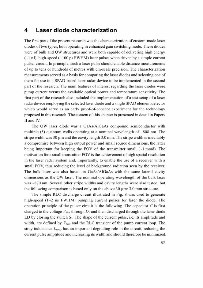
57
4 Laser diode characterization
The first part of the present research was the characterization of custom-made laser
diodes of two types, both operating in enhanced gain switching mode. These diodes
were of bulk and QW structures and were both capable of delivering high energy
(~1 nJ), high-speed (~100 ps FWHM) laser pulses when driven by a simple current
pulser circuit. In principle, such a laser pulse should enable distance measurements
of up to tens or hundreds of metres with cm-scale precision. The characterization
measurements served as a basis for comparing the laser diodes and selecting one of
them for use in a SPAD-based laser radar device to be implemented in the second
part of the research. The main features of interest regarding the laser diodes were
pump current versus the available optical power and temperature sensitivity. The
first part of the research also included the implementation of a test setup of a laser
radar device employing the selected laser diode and a single SPAD element detector
which would serve as an early proof-of-concept experiment for the technology
proposed in this research. The content of this chapter is presented in detail in Papers
II and IV.
The QW laser diode was a GaAs/AlGaAs compound semiconductor with
multiple (5) quantum wells operating at a nominal wavelength of ~808 nm. The
stripe width was 30 µm and the cavity length 3.0 mm. The stripe width is inevitably
a compromise between high output power and small source dimensions, the latter
being important for keeping the FOV of the transmitter small (~1 mrad). The
motivation for a small transmitter FOV is the achievement of high spatial resolution
in the laser radar system and, importantly, to enable the use of a receiver with a
small FOV, thus reducing the level of background radiation seen by the receiver.
The bulk laser was also based on GaAs/AlGaAs with the same lateral cavity
dimensions as the QW laser. The nominal operating wavelength of the bulk laser
was ~870 nm. Several other stripe widths and cavity lengths were also tested, but
the following comparison is based only on the above 30 µm/ 3.0 mm structure.
The simple RLC discharge circuit illustrated in Fig. 8 was used to generate
high-speed (1–2 ns FWHM) pumping current pulses for laser the diode. The
operation principle of the pulser circuit is the following. The capacitor C is first
charged to the voltage Vbias through D1 and then discharged through the laser diode
LD by closing the switch S1. The shape of the current pulse, i.e. its amplitude and
width, are defined by Vbias and the RLC transient of the pump current loop. The
stray inductance Lstray has an important degrading role in the circuit, reducing the
current pulse amplitude and increasing its width and should therefore be minimized.
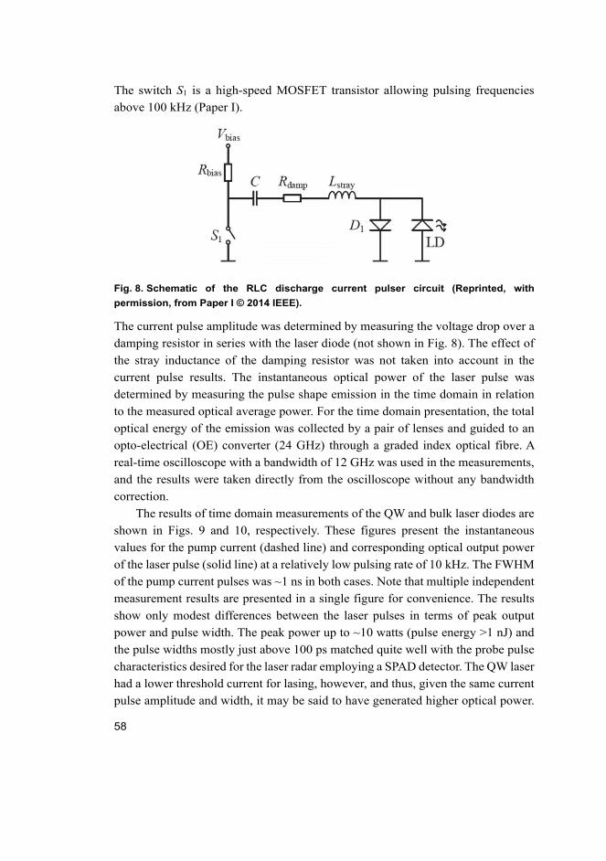
58
The switch S1 is a high-speed MOSFET transistor allowing pulsing frequencies
above 100 kHz (Paper I).
Fig. 8. Schematic of the RLC discharge current pulser circuit (Reprinted, with
permission, from Paper I © 2014 IEEE).
The current pulse amplitude was determined by measuring the voltage drop over a
damping resistor in series with the laser diode (not shown in Fig. 8). The effect of
the stray inductance of the damping resistor was not taken into account in the
current pulse results. The instantaneous optical power of the laser pulse was
determined by measuring the pulse shape emission in the time domain in relation
to the measured optical average power. For the time domain presentation, the total
optical energy of the emission was collected by a pair of lenses and guided to an
opto-electrical (OE) converter (24 GHz) through a graded index optical fibre. A
real-time oscilloscope with a bandwidth of 12 GHz was used in the measurements,
and the results were taken directly from the oscilloscope without any bandwidth
correction.
The results of time domain measurements of the QW and bulk laser diodes are
shown in Figs. 9 and 10, respectively. These figures present the instantaneous
values for the pump current (dashed line) and corresponding optical output power
of the laser pulse (solid line) at a relatively low pulsing rate of 10 kHz. The FWHM
of the pump current pulses was ~1 ns in both cases. Note that multiple independent
measurement results are presented in a single figure for convenience. The results
show only modest differences between the laser pulses in terms of peak output
power and pulse width. The peak power up to ~10 watts (pulse energy >1 nJ) and
the pulse widths mostly just above 100 ps matched quite well with the probe pulse
characteristics desired for the laser radar employing a SPAD detector. The QW laser
had a lower threshold current for lasing, however, and thus, given the same current
pulse amplitude and width, it may be said to have generated higher optical power.
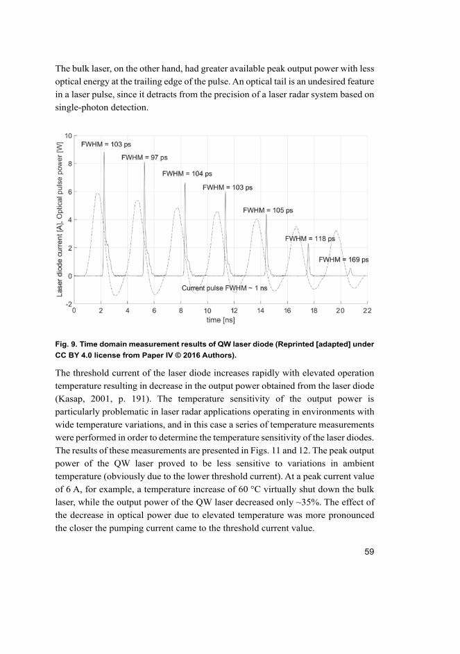
59
The bulk laser, on the other hand, had greater available peak output power with less
optical energy at the trailing edge of the pulse. An optical tail is an undesired feature
in a laser pulse, since it detracts from the precision of a laser radar system based on
single-photon detection.
Fig. 9. Time domain measurement results of QW laser diode (Reprinted [adapted] under
CC BY 4.0 license from Paper IV © 2016 Authors).
The threshold current of the laser diode increases rapidly with elevated operation
temperature resulting in decrease in the output power obtained from the laser diode
(Kasap, 2001, p. 191). The temperature sensitivity of the output power is
particularly problematic in laser radar applications operating in environments with
wide temperature variations, and in this case a series of temperature measurements
were performed in order to determine the temperature sensitivity of the laser diodes.
The results of these measurements are presented in Figs. 11 and 12. The peak output
power of the QW laser proved to be less sensitive to variations in ambient
temperature (obviously due to the lower threshold current). At a peak current value
of 6 A, for example, a temperature increase of 60 °C virtually shut down the bulk
laser, while the output power of the QW laser decreased only ~35%. The effect of
the decrease in optical power due to elevated temperature was more pronounced
the closer the pumping current came to the threshold current value.
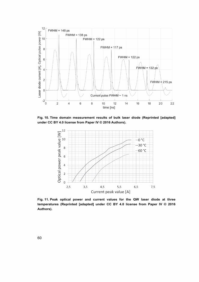
60
Fig. 10. Time domain measurement results of bulk laser diode (Reprinted [adapted]
under CC BY 4.0 license from Paper IV © 2016 Authors).
Fig. 11. Peak optical power and current values for the QW laser diode at three
temperatures (Reprinted [adapted] under CC BY 4.0 license from Paper IV © 2016
Authors).
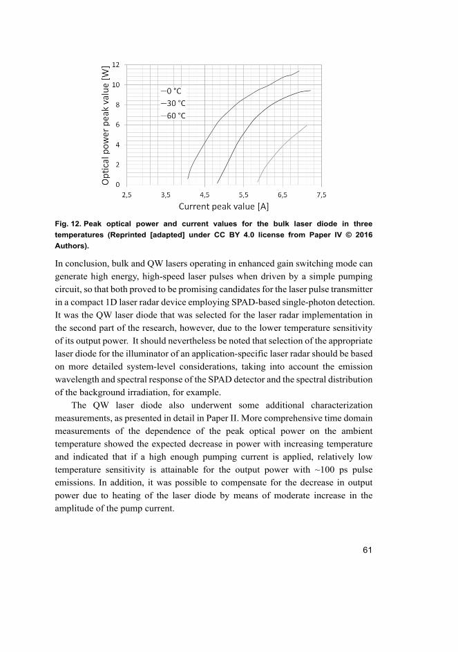
61
Fig. 12. Peak optical power and current values for the bulk laser diode in three
temperatures (Reprinted [adapted] under CC BY 4.0 license from Paper IV © 2016
Authors).
In conclusion, bulk and QW lasers operating in enhanced gain switching mode can
generate high energy, high-speed laser pulses when driven by a simple pumping
circuit, so that both proved to be promising candidates for the laser pulse transmitter
in a compact 1D laser radar device employing SPAD-based single-photon detection.
It was the QW laser diode that was selected for the laser radar implementation in
the second part of the research, however, due to the lower temperature sensitivity
of its output power. It should nevertheless be noted that selection of the appropriate
laser diode for the illuminator of an application-specific laser radar should be based
on more detailed system-level considerations, taking into account the emission
wavelength and spectral response of the SPAD detector and the spectral distribution
of the background irradiation, for example.
The QW laser diode also underwent some additional characterization
measurements, as presented in detail in Paper II. More comprehensive time domain
measurements of the dependence of the peak optical power on the ambient
temperature showed the expected decrease in power with increasing temperature
and indicated that if a high enough pumping current is applied, relatively low
temperature sensitivity is attainable for the output power with ~100 ps pulse
emissions. In addition, it was possible to compensate for the decrease in output
power due to heating of the laser diode by means of moderate increase in the
amplitude of the pump current.
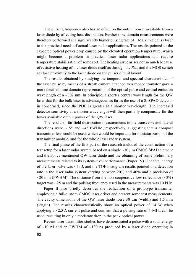
62
The pulsing frequency also has an effect on the output power available from a
laser diode by affecting heat dissipation. Further time domain measurements were
therefore performed at a significantly higher pulsing rate of 1 MHz, which is closer
to the practical needs of actual laser radar applications. The results pointed to the
expected optical power drop caused by the elevated operation temperature, which
might become a problem in practical laser radar applications and require
temperature stabilization of some sort. The heating issue arises not so much because
of resistive heating of the laser diode itself as through the Rbias and the MOS switch
at close proximity to the laser diode on the pulser circuit layout.
The results obtained by studying the temporal and spectral characteristics of
the laser pulse by means of a streak camera attached to a monochromator gave a
more detailed time domain representation of the optical pulse and central emission
wavelength of a ~802 nm. In principle, a shorter central wavelength for the QW
laser that for the bulk laser is advantageous as far as the use of a Si SPAD detector
in concerned, since the PDE is greater at a shorter wavelength. The increased
detector sensitivity at a shorter wavelength will then partially compensate for the
lower available output power of the QW laser.
The results of far field distribution measurements in the transverse and lateral
directions were ~15° and ~4° FWHM, respectively, suggesting that a compact
transmitter lens could be used, which would be important for miniaturization of the
transmitter module, and for the whole laser radar system.
The final phase of the first part of the research included the construction of a
test setup for a laser radar system based on a single ~30 µm CMOS SPAD element
and the above-mentioned QW laser diode and the obtaining of some preliminary
measurements related to its system-level performance (Paper IV). The total energy
of the laser pulse was ~1 nJ, and the TOF histogram results pointed to a detection
rate in the laser radar system varying between 20% and 40% and a precision of
~20 mm (FWHM). The distance from the non-cooperative low reflectance (~3%)
target was ~25 m and the pulsing frequency used in the measurements was 10 kHz.
Paper II also briefly describes the realization of a prototype transmitter
employing a full-custom CMOS laser driver and present some test measurements.
The cavity dimensions of the QW laser diode were 30 µm (width) and 1.5 mm
(length). The results characteristically show an optical power of ~4 W when
applying a ~2.5 A current pulse and confirm that a pulsing rate of 1 MHz can be
used, resulting in only a moderate drop in the peak optical power.
Recent laser transmitter studies have demonstrated a pulse with a total energy
of ~10 nJ and an FWHM of ~130 ps produced by a laser diode operating in
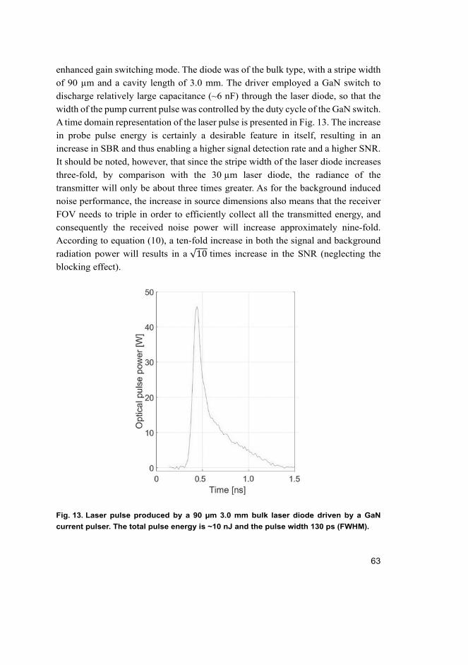
63
enhanced gain switching mode. The diode was of the bulk type, with a stripe width
of 90 µm and a cavity length of 3.0 mm. The driver employed a GaN switch to
discharge relatively large capacitance (~6 nF) through the laser diode, so that the
width of the pump current pulse was controlled by the duty cycle of the GaN switch.
A time domain representation of the laser pulse is presented in Fig. 13. The increase
in probe pulse energy is certainly a desirable feature in itself, resulting in an
increase in SBR and thus enabling a higher signal detection rate and a higher SNR.
It should be noted, however, that since the stripe width of the laser diode increases
three-fold, by comparison with the 30 µm laser diode, the radiance of the
transmitter will only be about three times greater. As for the background induced
noise performance, the increase in source dimensions also means that the receiver
FOV needs to triple in order to efficiently collect all the transmitted energy, and
consequently the received noise power will increase approximately nine-fold.
According to equation (10), a ten-fold increase in both the signal and background
radiation power will results in a √10 times increase in the SNR (neglecting the
blocking effect).
Fig. 13. Laser pulse produced by a 90 µm 3.0 mm bulk laser diode driven by a GaN
current pulser. The total pulse energy is ~10 nJ and the pulse width 130 ps (FWHM).

64
65
5 Design principles and implementation of a 1D laser radar employing a SPAD detector array
This chapter describes the design principles and implementation of a 1D
single-photon detection laser radar system, based on high energy, high-speed laser
pulses and a 2D CMOS SPAD detector array. The purpose of the prototype
implementation was to study the key features related to actual SPAD-based laser
radar systems, such as the limits of their performance and the supposed beneficial
features enabled by the use of a SPAD array with exclusive TDC channels for 1D
laser radar distance measurements. The implementation also served as a
verification that the proposed technology could not only result in a high
performance, cost-effective laser radar system but also render its overall
implementation more compact.
The key feature of the proposed laser radar system, in addition to a sub-ns laser
pulse transmitter, was to employ a 2D SPAD detector array to realize the following
functions. One characteristic feature of a laser radar system with biaxial optics is
target distance-dependent laser spot wander on the detector surface, which entails
a requirement for a sufficiently large-sized detector. The problem with a large
detector, however, is that it will increase the reception of background radiation
power as well, at the risk of masking and blocking the SPAD detector. For this
reason, the proposed system contains a selectable subarray feature that enables spot
tracking on the detector surface while maintaining a small effective FOV and
minimizing both background power reception and its masking and blocking effects.
Moreover, the selectable subarray feature will also raise the prospect of walk
error-free measurements in the case of probe pulse echoes of great magnitude.
The implementation of the laser radar system is based on the structure and
operating principle presented in the block diagram of a pulsed TOF laser radar in
Fig. 1. The laser transmitter module contains a QW laser diode, operating in
enhanced gain switching mode and generating a high energy (~1 nJ), high-speed
(~100 ps FWHM) probe pulse driven by a simple pump current circuit. The receiver
module is a custom-made single-chip IC integrating a 2D SPAD detector array, with
its associated electronics, and a multichannel TDC circuit for multiple independent
TOF measurements. One important aim of the implementation, besides the
performance parameters, was to achieve a laser radar system of compact overall
size.
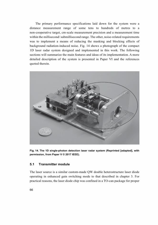
66
The primary performance specifications laid down for the system were a
distance measurement range of some tens to hundreds of metres to a
non-cooperative target, cm-scale measurement precision and a measurement time
within the millisecond/ submillisecond range. The other, noise-related requirements
was to implement a means of reducing the masking and blocking effects of
background radiation-induced noise. Fig. 14 shows a photograph of the compact
1D laser radar system designed and implemented in this work. The following
sections will summarize the main features and ideas of its implementation. A more
detailed description of the system is presented in Paper VI and the references
quoted therein.
Fig. 14. The 1D single-photon detection laser radar system (Reprinted [adapted], with
permission, from Paper V © 2017 IEEE).
5.1 Transmitter module
The laser source is a similar custom-made QW double heterostructure laser diode
operating in enhanced gain switching mode to that described in chapter 3. For
practical reasons, the laser diode chip was confined in a TO-can package for proper

67
protection against operation environment hazards. The laser diode was pumped by
a simple RLC discharge circuit similar to that likewise presented in chapter 3. The
time domain measurements of the pump current pulse and corresponding laser
pulse are presented in Fig. 15. The peak current pulse value of 4 A and the width
of 1 ns FWHM together generate an optical pulse with a peak power of 5 W and
width of 100 ps FWHM. The total energy of the laser pulse is ~0.6 nJ. The pulsing
frequency applied in the laser radar system was 100 kHz. The transmitter circuit
also generates a start signal from the pump current pulse to initiate TOF
measurement.
Fig. 15. The pump current pulse and laser pulse generated by the 30 µm 3.0 mm QW
laser diode (Reprinted [adapted] under CC BY 4.0 license from Paper VI © 2018 Authors).
A photograph of the single PCB implementation including both its transmitter and
receiver electronics and its physical dimensions is shown in Fig. 16. The distance
between the laser source and the receiver IC is ~20 mm. Equations
𝑖
𝑉
𝑅𝐿𝐶
(13)
and
FWHM 2 ∙ 𝐿 ∙ 𝐶 (14)
are used to estimate the amplitude and FWHM of the current pulse generated by
the RLC pulser circuit (Nissinen & Kostamovaara, 2013). As can be seen in the
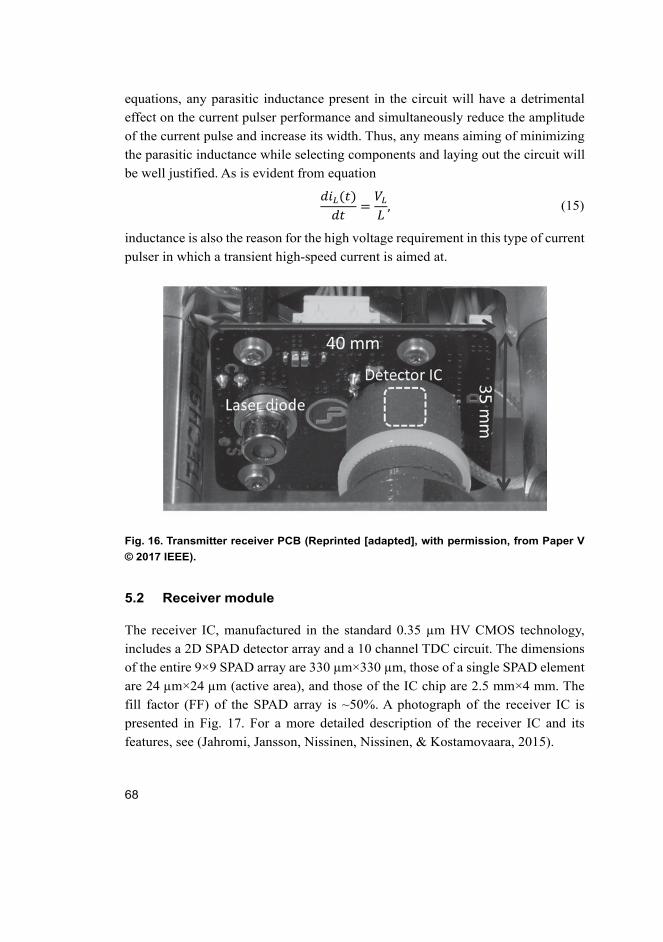
68
equations, any parasitic inductance present in the circuit will have a detrimental
effect on the current pulser performance and simultaneously reduce the amplitude
of the current pulse and increase its width. Thus, any means aiming of minimizing
the parasitic inductance while selecting components and laying out the circuit will
be well justified. As is evident from equation
𝑑𝑖 𝑡𝑑𝑡
𝑉𝐿
, (15)
inductance is also the reason for the high voltage requirement in this type of current
pulser in which a transient high-speed current is aimed at.
Fig. 16. Transmitter receiver PCB (Reprinted [adapted], with permission, from Paper V
© 2017 IEEE).
5.2 Receiver module
The receiver IC, manufactured in the standard 0.35 µm HV CMOS technology,
includes a 2D SPAD detector array and a 10 channel TDC circuit. The dimensions
of the entire 9×9 SPAD array are 330 µm×330 µm, those of a single SPAD element
are 24 µm×24 µm (active area), and those of the IC chip are 2.5 mm×4 mm. The
fill factor (FF) of the SPAD array is ~50%. A photograph of the receiver IC is
presented in Fig. 17. For a more detailed description of the receiver IC and its
features, see (Jahromi, Jansson, Nissinen, Nissinen, & Kostamovaara, 2015).
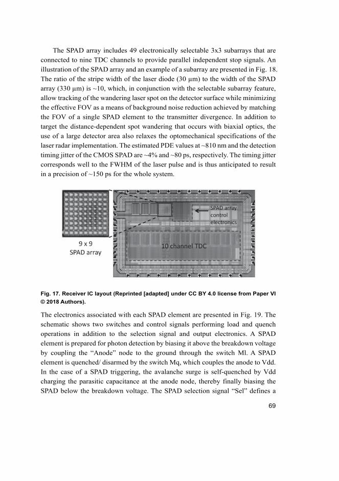
69
The SPAD array includes 49 electronically selectable 3x3 subarrays that are
connected to nine TDC channels to provide parallel independent stop signals. An
illustration of the SPAD array and an example of a subarray are presented in Fig. 18.
The ratio of the stripe width of the laser diode (30 µm) to the width of the SPAD
array (330 µm) is ~10, which, in conjunction with the selectable subarray feature,
allow tracking of the wandering laser spot on the detector surface while minimizing
the effective FOV as a means of background noise reduction achieved by matching
the FOV of a single SPAD element to the transmitter divergence. In addition to
target the distance-dependent spot wandering that occurs with biaxial optics, the
use of a large detector area also relaxes the optomechanical specifications of the
laser radar implementation. The estimated PDE values at ~810 nm and the detection
timing jitter of the CMOS SPAD are ~4% and ~80 ps, respectively. The timing jitter
corresponds well to the FWHM of the laser pulse and is thus anticipated to result
in a precision of ~150 ps for the whole system.
Fig. 17. Receiver IC layout (Reprinted [adapted] under CC BY 4.0 license from Paper VI
© 2018 Authors).
The electronics associated with each SPAD element are presented in Fig. 19. The
schematic shows two switches and control signals performing load and quench
operations in addition to the selection signal and output electronics. A SPAD
element is prepared for photon detection by biasing it above the breakdown voltage
by coupling the “Anode” node to the ground through the switch Ml. A SPAD
element is quenched/ disarmed by the switch Mq, which couples the anode to Vdd.
In the case of a SPAD triggering, the avalanche surge is self-quenched by Vdd
charging the parasitic capacitance at the anode node, thereby finally biasing the
SPAD below the breakdown voltage. The SPAD selection signal “Sel” defines a
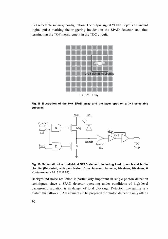
70
3x3 selectable subarray configuration. The output signal “TDC Stop” is a standard
digital pulse marking the triggering incident in the SPAD detector, and thus
terminating the TOF measurement in the TDC circuit.
Fig. 18. Illustration of the 9x9 SPAD array and the laser spot on a 3x3 selectable
subarray.
Fig. 19. Schematic of an individual SPAD element, including load, quench and buffer
circuits (Reprinted, with permission, from Jahromi, Jansson, Nissinen, Nissinen, &
Kostamovaara 2015 © IEEE).
Background noise reduction is particularly important in single-photon detection
techniques, since a SPAD detector operating under conditions of high-level
background radiation is in danger of total blockage. Detector time gating is a
feature that allows SPAD elements to be prepared for photon detection only after a
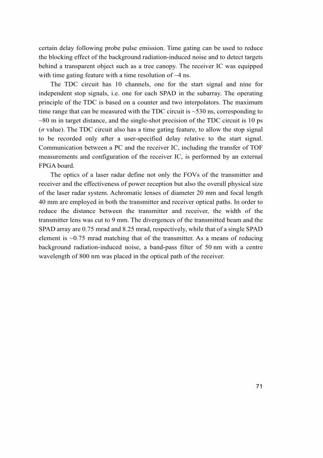
71
certain delay following probe pulse emission. Time gating can be used to reduce
the blocking effect of the background radiation-induced noise and to detect targets
behind a transparent object such as a tree canopy. The receiver IC was equipped
with time gating feature with a time resolution of ~4 ns.
The TDC circuit has 10 channels, one for the start signal and nine for
independent stop signals, i.e. one for each SPAD in the subarray. The operating
principle of the TDC is based on a counter and two interpolators. The maximum
time range that can be measured with the TDC circuit is ~530 ns, corresponding to
~80 m in target distance, and the single-shot precision of the TDC circuit is 10 ps
(σ value). The TDC circuit also has a time gating feature, to allow the stop signal
to be recorded only after a user-specified delay relative to the start signal.
Communication between a PC and the receiver IC, including the transfer of TOF
measurements and configuration of the receiver IC, is performed by an external
FPGA board.
The optics of a laser radar define not only the FOVs of the transmitter and
receiver and the effectiveness of power reception but also the overall physical size
of the laser radar system. Achromatic lenses of diameter 20 mm and focal length
40 mm are employed in both the transmitter and receiver optical paths. In order to
reduce the distance between the transmitter and receiver, the width of the
transmitter lens was cut to 9 mm. The divergences of the transmitted beam and the
SPAD array are 0.75 mrad and 8.25 mrad, respectively, while that of a single SPAD
element is ~0.75 mrad matching that of the transmitter. As a means of reducing
background radiation-induced noise, a band-pass filter of 50 nm with a centre
wavelength of 800 nm was placed in the optical path of the receiver.

72

73
6 Characterization of the 1D laser radar
A series of characterization measurements were carried out in order to determine
the key system-level performance parameters of the prototype 1D compact single
photon laser radar system presented in chapter 4. The performance parameters of
interest included walk error, linearity, signal detection rate and precision. The same
characterization measurements also served to demonstrate some novel features of
the system that had been actualized by the application of a 2D detector array
configuration. One such feature was the availability of walk error-free distance
measurements, thanks to the distribution of the laser energy spot over the detector
array and the selectable subarray feature, thereby improving the measurement
accuracy of the system.
Additional measurements were performed to study means of reducing
background radiation-induced false detections, i.e. noise and its masking and
blocking effects. The means studied here are detector time gating and variation in
the size of the receiver aperture. The reduction of background radiation-induced
masking and blocking effects would potentially increase the SNR and therefore
have a desirable effect on the measurement range and speed under conditions of
high-level background radiation, e.g. outdoors. Additional measurements also
included two feasibility studies intended to demonstrate the longitudinal and
transversal spatial accuracy of the 1D laser radar system in a practical measurement
situation. In the first study the system was employed to measure the heartbeat of a
test subject by virtue of the sub-mm measurement precision of the system, and in
the second the system was shown to be capable of distinguishing individual
free-falling snowflakes.
This chapter describes the main details of the measurement setups, the results
and their implications. The key parameters of the laser radar system, repeated here
for convenience, are a probe pulse energy of 0.6 nJ and FWHM of 100 ps, an
applied transmitter pulsing frequency of 100 kHz, a receiver aperture area
of 3.14·10-4 m2 (diameter 20 mm) and an estimated PDE of the Si SPAD detector
element at ~810 nm is 4%. The transmitter beam divergence is 0.75 mrad and that
of the whole 9x9 detector array 8.25 mrad. A more detailed account of the specifics
of the characterization measurements and their setups is presented in the
characterization measurements section of Paper VI.
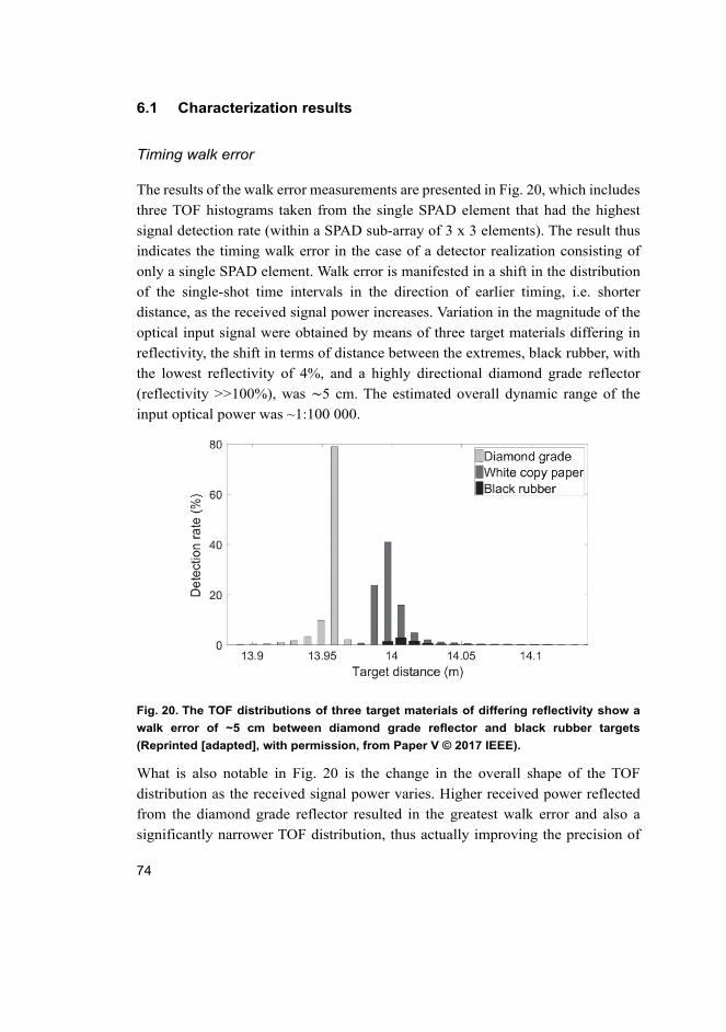
74
6.1 Characterization results
Timing walk error
The results of the walk error measurements are presented in Fig. 20, which includes
three TOF histograms taken from the single SPAD element that had the highest
signal detection rate (within a SPAD sub-array of 3 x 3 elements). The result thus
indicates the timing walk error in the case of a detector realization consisting of
only a single SPAD element. Walk error is manifested in a shift in the distribution
of the single-shot time intervals in the direction of earlier timing, i.e. shorter
distance, as the received signal power increases. Variation in the magnitude of the
optical input signal were obtained by means of three target materials differing in
reflectivity, the shift in terms of distance between the extremes, black rubber, with
the lowest reflectivity of 4%, and a highly directional diamond grade reflector
(reflectivity >>100%), was ∼5 cm. The estimated overall dynamic range of the
input optical power was ~1:100 000.
Fig. 20. The TOF distributions of three target materials of differing reflectivity show a
walk error of ~5 cm between diamond grade reflector and black rubber targets
(Reprinted [adapted], with permission, from Paper V © 2017 IEEE).
What is also notable in Fig. 20 is the change in the overall shape of the TOF
distribution as the received signal power varies. Higher received power reflected
from the diamond grade reflector resulted in the greatest walk error and also a
significantly narrower TOF distribution, thus actually improving the precision of
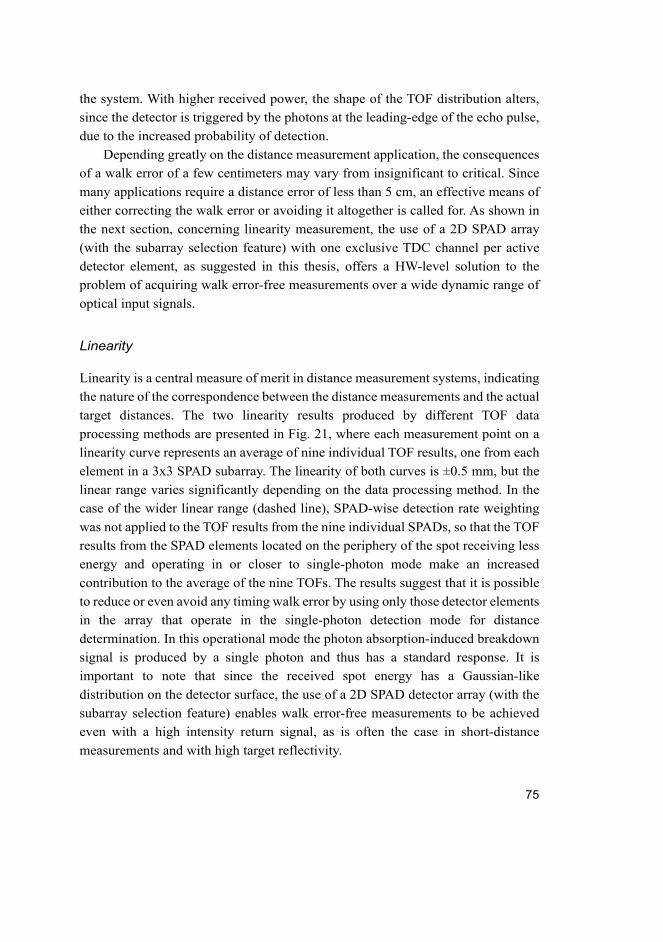
75
the system. With higher received power, the shape of the TOF distribution alters,
since the detector is triggered by the photons at the leading-edge of the echo pulse,
due to the increased probability of detection.
Depending greatly on the distance measurement application, the consequences
of a walk error of a few centimeters may vary from insignificant to critical. Since
many applications require a distance error of less than 5 cm, an effective means of
either correcting the walk error or avoiding it altogether is called for. As shown in
the next section, concerning linearity measurement, the use of a 2D SPAD array
(with the subarray selection feature) with one exclusive TDC channel per active
detector element, as suggested in this thesis, offers a HW-level solution to the
problem of acquiring walk error-free measurements over a wide dynamic range of
optical input signals.
Linearity
Linearity is a central measure of merit in distance measurement systems, indicating
the nature of the correspondence between the distance measurements and the actual
target distances. The two linearity results produced by different TOF data
processing methods are presented in Fig. 21, where each measurement point on a
linearity curve represents an average of nine individual TOF results, one from each
element in a 3x3 SPAD subarray. The linearity of both curves is ±0.5 mm, but the
linear range varies significantly depending on the data processing method. In the
case of the wider linear range (dashed line), SPAD-wise detection rate weighting
was not applied to the TOF results from the nine individual SPADs, so that the TOF
results from the SPAD elements located on the periphery of the spot receiving less
energy and operating in or closer to single-photon mode make an increased
contribution to the average of the nine TOFs. The results suggest that it is possible
to reduce or even avoid any timing walk error by using only those detector elements
in the array that operate in the single-photon detection mode for distance
determination. In this operational mode the photon absorption-induced breakdown
signal is produced by a single photon and thus has a standard response. It is
important to note that since the received spot energy has a Gaussian-like
distribution on the detector surface, the use of a 2D SPAD detector array (with the
subarray selection feature) enables walk error-free measurements to be achieved
even with a high intensity return signal, as is often the case in short-distance
measurements and with high target reflectivity.
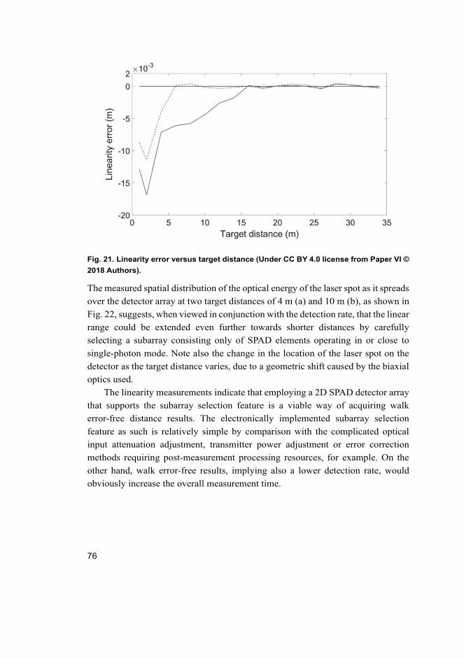
76
Fig. 21. Linearity error versus target distance (Under CC BY 4.0 license from Paper VI ©
2018 Authors).
The measured spatial distribution of the optical energy of the laser spot as it spreads
over the detector array at two target distances of 4 m (a) and 10 m (b), as shown in
Fig. 22, suggests, when viewed in conjunction with the detection rate, that the linear
range could be extended even further towards shorter distances by carefully
selecting a subarray consisting only of SPAD elements operating in or close to
single-photon mode. Note also the change in the location of the laser spot on the
detector as the target distance varies, due to a geometric shift caused by the biaxial
optics used.
The linearity measurements indicate that employing a 2D SPAD detector array
that supports the subarray selection feature is a viable way of acquiring walk
error-free distance results. The electronically implemented subarray selection
feature as such is relatively simple by comparison with the complicated optical
input attenuation adjustment, transmitter power adjustment or error correction
methods requiring post-measurement processing resources, for example. On the
other hand, walk error-free results, implying also a lower detection rate, would
obviously increase the overall measurement time.
77
Fig. 22. Energy distribution of a laser spot image on a 9x9 SPAD array (Reprinted
[adapted], with permission, from Paper V © 2017 IEEE).
Another measurement was carried out in order to demonstrate the availability of
walk error-free distance measurement result enabled by the application of a 2D
SPAD array configuration. The measurement setup included a highly reflective
(diamond grade) target located ~4 m from the laser radar system, resulting in a
probe pulse echo of great magnitude. The resulting measurements are shown in
Fig. 23, which presents two normalized single-shot TOF distributions from two
SPAD elements residing in different subarrays. The left (narrower bars) and right
distributions were acquired from SPAD elements with detection rates of ~99% and
~5%, respectively. The SPAD element with the higher detection rate belongs to a
subarray at the centre of which the laser spot is located, while the other SPAD
element belongs to the subarray furthest away from the laser spot. The results
demonstrate that a walk error of ~4 cm (measured from histogram peaks) is
completely avoidable by careful selection of a SPAD element operating in
single-photon detection mode (detection rate <10%) for actual distance
determination.
78
Fig. 23. The TOF distributions of two SPAD elements in different subarrays show a walk
error of ~4 cm. Detection rates were ~99% (left) and ~5% (right).
Signal detection rate
The signal detection rate is defined here as the ratio of the sum of the combined
signal detection counts of the nine SPAD elements to the total count of emitted
probe pulses. Along with pulsing frequency, the signal detection rate defines the
actual measurement rate and the overall measurement time. The detection rate is
also indicative of the mode of photon detection, i.e. single or multiphoton detection,
and is thus also associated with walk error and precision. The radar equation (3)
typically serves as the basis for a theoretical estimation of the detection rate of an
actual laser radar system.
The results of detection rate measurement versus target distance, along with a
theoretical reference curve based on the radar equation, are presented in Fig. 24,
where the solid line represents the combined measurement rate curve for the nine
SPAD elements (max. value 900%) and the dashed line is the reference curve. The
signal detection rate is ~28% when measured while the target is located 34 m from
the laser radar system. The parameters of the radar equation employed here are:
transmitted pulse energy Epulse of 0.6 nJ, optical efficiency τ of 80%, aperture area
AR of 3.14·10-4 m2 and target reflectivity ϵ of 11%. The other, less certain,
parameters and their values are: SPAD array fill factor FF of ~50%, photon
detection efficiency PDE of 4% and receiver optical bandpass filter efficiency of
79
75%. The curves deviate from each other within a distance range of less than ~20 m.
Higher received power and increased spot size result in a situation in which an
increasing number of SPAD elements are operating in multiphoton mode, i.e. at
some degree of saturation, as manifested in saturation of the detection rate as well.
The steep collapse of the detection rate at target distances of <4 m, on the other
hand, is caused by the spot finally wandering outside the detector array (Wang &
Kostamovaara, 1994). Another effect that reduces the detection rate is the dispersal
of the energy of the laser spot over a larger area than the subarray, due to defocusing
of the optics, so that only a fraction of the spot energy falls onto the subarray.
Fig. 24. Combined detection rate of nine SPADs versus target distance (Under CC BY
4.0 license from Paper VI © 2018 Authors).
Measurement precision
The precision of a distance measurement system is a measure of the uncertainty of
a single valid measurement result (detection of a signal photon), and consequently
it is a crucial factor contributing to the overall measurement accuracy obtainable
from the system. The main factors detracting from the precision of TOF
measurements in a SPAD-based laser radar are the probe pulse width and the timing
jitter of the SPAD detector. In the present work precision is defined as the FWHM
of the measured TOF distribution of signal detections.
Single-shot time interval histogram of the single SPAD with the highest
detection rate at a target distance of 34 m is shown in Fig. 25. The FWHM of the
80
histogram, based on a bin width of 65 ps, is 130 ps, corresponding to a distance
measurement precision of ~2 cm. The signal detection rate was ~10%. This single
shot measurement result corresponds fairly well to the theoretical estimate of the
precision (√tpulse FWHM2 tSPAD jitter
2), in which the predominating factors in TOF jitter,
i.e. the probe pulse FWHM and the timing jitter of a typical shallow silicon SPAD,
are 100 ps and 80 ps, respectively.
Fig. 25. Measurement precision of a laser radar system (Reprinted [adapted], with
permission, from Paper V © 2017 IEEE).
Reduction of the background radiation-induced detector blocking effect
A series of outdoor distance measurements were carried out in order to study the
effect of photodetector time gating and the size of the receiver aperture on masking
and blocking effects under conditions of a high level of background radiation. From
the point of view of noise induced by background photons, a single-photon
detection system that is capable of only one detection per probe pulse has a
significant inherent drawback. Any false photon detection prior to the arrival of the
signal photons will potentially prevent (i.e. mask) the detection of a signal photon,
thus causing a decrease in the available signal detection rate and SNR. In outdoor
applications in bright sunlight a high rate of background photons may in the worst
case totally block signal photons from the detector, thus rendering the target
non-existent, whereas with optimal time gating the photodetector element can be
prepared for detection immediately before the arrival of the signal photons, thus
minimizing the probability of prior background photon detection. The problem
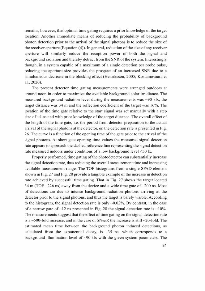
81
remains, however, that optimal time gating requires a prior knowledge of the target
location. Another immediate means of reducing the probability of background
photon detection prior to the arrival of the signal photons is to reduce the size of
the receiver aperture (Equation (4)). In general, reduction of the size of any receiver
aperture will similarly reduce the reception power of both the signal and
background radiation and thereby detract from the SNR of the system. Interestingly
though, in a system capable of a maximum of a single detection per probe pulse,
reducing the aperture size provides the prospect of an increased SNR due to a
simultaneous decrease in the blocking effect (Henriksson, 2005; Kostamovaara et
al., 2020).
The present detector time gating measurements were arranged outdoors at
around noon in order to maximize the available background solar irradiance. The
measured background radiation level during the measurements was ~90 klx, the
target distance was 34 m and the reflection coefficient of the target was 16%. The
location of the time gate relative to the start signal was set manually with a step
size of ~4 ns and with prior knowledge of the target distance. The overall effect of
the length of the time gate, i.e. the period from detector preparation to the actual
arrival of the signal photons at the detector, on the detection rate is presented in Fig.
26. The curve is a function of the opening time of the gate prior to the arrival of the
signal photons. At short gate opening time values the measured signal detection
rate appears to approach the dashed reference line representing the signal detection
rate measured indoors under conditions of a low background level <50 lx.
Properly performed, time gating of the photodetector can substantially increase
the signal detection rate, thus reducing the overall measurement time and increasing
available measurement range. The TOF histograms from a single SPAD element
shown in Fig. 27 and Fig. 28 provide a tangible example of the increase in detection
rate achieved by successful time gating. That in Fig. 27 shows the target located
34 m (TOF ~226 ns) away from the device and a wide time gate of ~200 ns. Most
of detections are due to intense background radiation photons arriving at the
detector prior to the signal photons, and thus the target is barely visible. According
to the histogram, the signal detection rate is only ~0.02%. By contrast, in the case
of a narrow gate of ~12 ns presented in Fig. 28 the signal detection rate is ~10%.
The measurements suggest that the effect of time gating on the signal detection rate
is a ~500-fold increase, and in the case of SNBGR the increase is still ~20-fold. The
estimated mean time between the background photon induced detections, as
calculated from the exponential decay, is ~35 ns, which corresponds to a
background illumination level of ~90 klx with the given system parameters. The
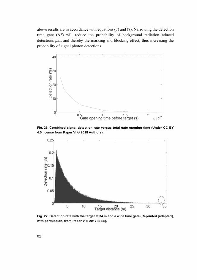
82
above results are in accordance with equations (7) and (8). Narrowing the detection
time gate (ΔT) will reduce the probability of background radiation-induced
detections pdet, and thereby the masking and blocking effect, thus increasing the
probability of signal photon detections.
Fig. 26. Combined signal detection rate versus total gate opening time (Under CC BY
4.0 license from Paper VI © 2018 Authors).
Fig. 27. Detection rate with the target at 34 m and a wide time gate (Reprinted [adapted],
with permission, from Paper V © 2017 IEEE).

83
Fig. 28. Detection rate with the target at 34 m and a narrow time gate (Reprinted
[adapted], with permission, from Paper V © 2017 IEEE).
In conclusion, detector time gating is an effective means of preventing background
photons from blocking the detector in single-photon detection-based laser ranging.
On the other hand, with high-level background illumination the SNR is still limited
by background detections, so that intensive averaging of successive measurements
is needed. Given the results in Figs. 27 and 28, for example, the probability of
background detection in the first measurement channels will be around 0.2%
(~65 ps∕34 ns), and if the signal detection rate were at the same level, a few
thousand laser shots would be needed to get a detectable signal included in the
histogram of the results (~10 000 shots for an SNR of ~5).
The effect of the size of the receiver aperture on background photon-induced
masking and blocking effects was studied by placing two smaller apertures
(diameters of 9 and 4 mm) in front of the receiver lens. Since the inherent receiver
aperture diameter was 18.4 mm, the above apertures were equal to 4-fold and
20-fold decreases in aperture area. The aperture measurements were performed
outdoors in conditions of high-level (~100 klx) solar background radiation. The
target had a reflection coefficient of ~12% and was located at 34 m.
The aperture measurements in Fig. 29 show raw data for three TOF
distributions in a certain SPAD element, corresponding to three aperture sizes. The
decrease in background radiation power along with the size of the aperture results
in an increase in the mean time between the background photon detections, in
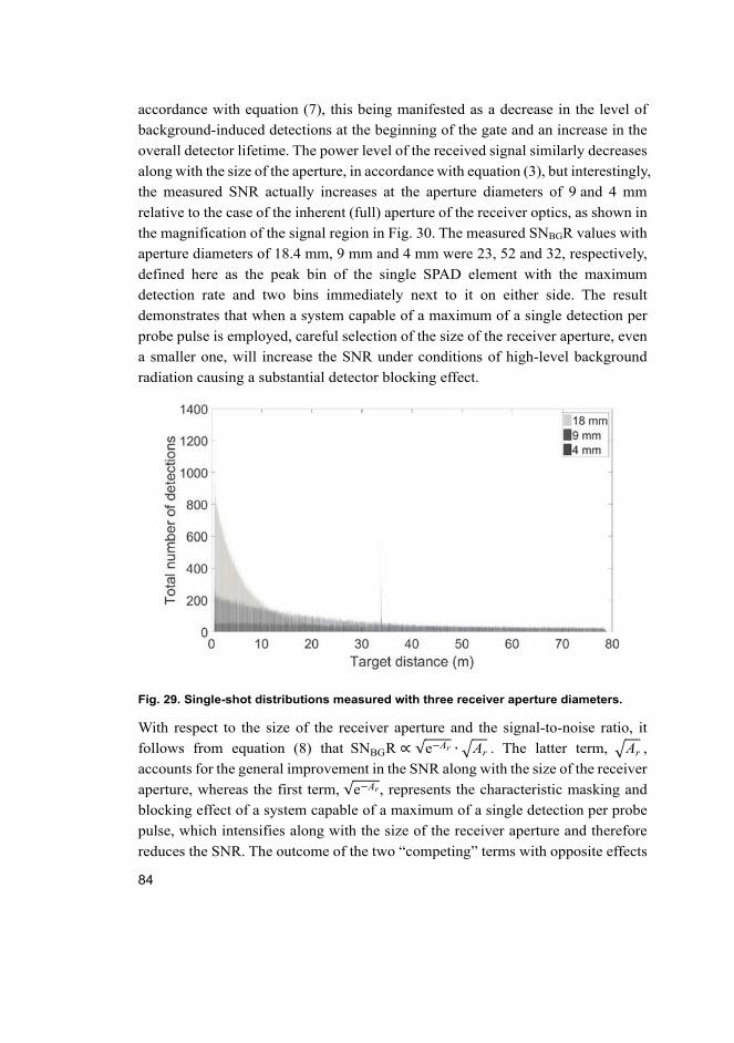
84
accordance with equation (7), this being manifested as a decrease in the level of
background-induced detections at the beginning of the gate and an increase in the
overall detector lifetime. The power level of the received signal similarly decreases
along with the size of the aperture, in accordance with equation (3), but interestingly,
the measured SNR actually increases at the aperture diameters of 9 and 4 mm
relative to the case of the inherent (full) aperture of the receiver optics, as shown in
the magnification of the signal region in Fig. 30. The measured SNBGR values with
aperture diameters of 18.4 mm, 9 mm and 4 mm were 23, 52 and 32, respectively,
defined here as the peak bin of the single SPAD element with the maximum
detection rate and two bins immediately next to it on either side. The result
demonstrates that when a system capable of a maximum of a single detection per
probe pulse is employed, careful selection of the size of the receiver aperture, even
a smaller one, will increase the SNR under conditions of high-level background
radiation causing a substantial detector blocking effect.
Fig. 29. Single-shot distributions measured with three receiver aperture diameters.
With respect to the size of the receiver aperture and the signal-to-noise ratio, it
follows from equation (8) that SNBGR ∝ √e Ar ∙ Ar . The latter term, Ar ,
accounts for the general improvement in the SNR along with the size of the receiver
aperture, whereas the first term, √e Ar, represents the characteristic masking and
blocking effect of a system capable of a maximum of a single detection per probe
pulse, which intensifies along with the size of the receiver aperture and therefore
reduces the SNR. The outcome of the two “competing” terms with opposite effects
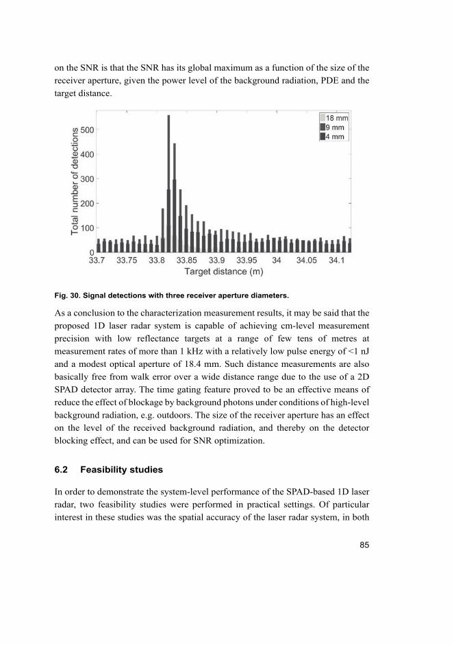
85
on the SNR is that the SNR has its global maximum as a function of the size of the
receiver aperture, given the power level of the background radiation, PDE and the
target distance.
Fig. 30. Signal detections with three receiver aperture diameters.
As a conclusion to the characterization measurement results, it may be said that the
proposed 1D laser radar system is capable of achieving cm-level measurement
precision with low reflectance targets at a range of few tens of metres at
measurement rates of more than 1 kHz with a relatively low pulse energy of <1 nJ
and a modest optical aperture of 18.4 mm. Such distance measurements are also
basically free from walk error over a wide distance range due to the use of a 2D
SPAD detector array. The time gating feature proved to be an effective means of
reduce the effect of blockage by background photons under conditions of high-level
background radiation, e.g. outdoors. The size of the receiver aperture has an effect
on the level of the received background radiation, and thereby on the detector
blocking effect, and can be used for SNR optimization.
6.2 Feasibility studies
In order to demonstrate the system-level performance of the SPAD-based 1D laser
radar, two feasibility studies were performed in practical settings. Of particular
interest in these studies was the spatial accuracy of the laser radar system, in both
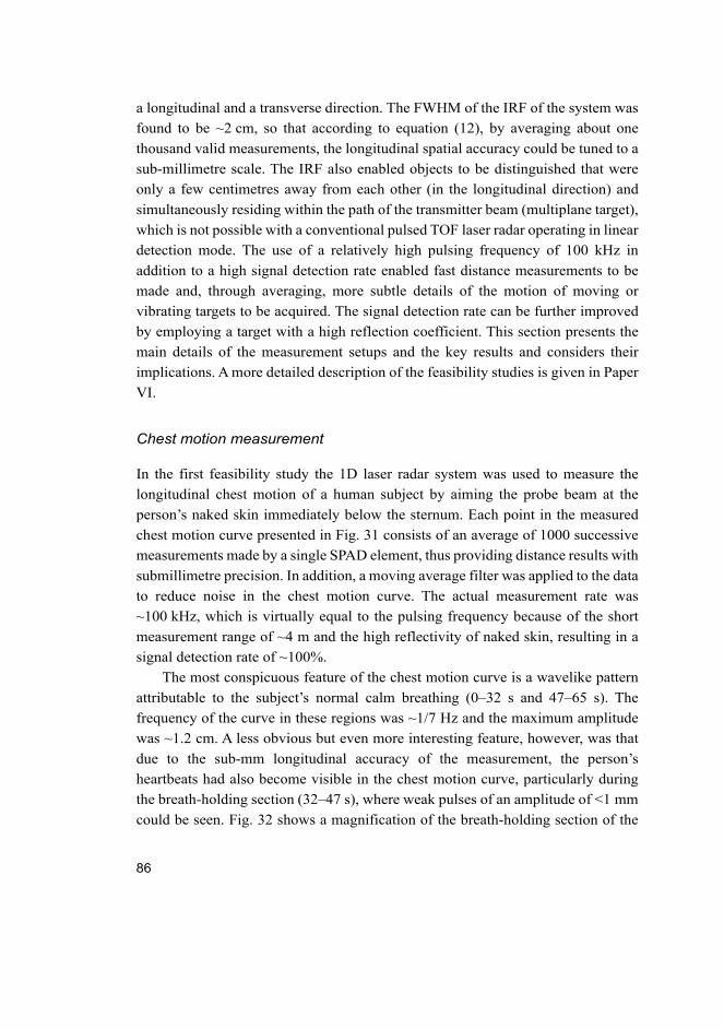
86
a longitudinal and a transverse direction. The FWHM of the IRF of the system was
found to be ~2 cm, so that according to equation (12), by averaging about one
thousand valid measurements, the longitudinal spatial accuracy could be tuned to a
sub-millimetre scale. The IRF also enabled objects to be distinguished that were
only a few centimetres away from each other (in the longitudinal direction) and
simultaneously residing within the path of the transmitter beam (multiplane target),
which is not possible with a conventional pulsed TOF laser radar operating in linear
detection mode. The use of a relatively high pulsing frequency of 100 kHz in
addition to a high signal detection rate enabled fast distance measurements to be
made and, through averaging, more subtle details of the motion of moving or
vibrating targets to be acquired. The signal detection rate can be further improved
by employing a target with a high reflection coefficient. This section presents the
main details of the measurement setups and the key results and considers their
implications. A more detailed description of the feasibility studies is given in Paper
VI.
Chest motion measurement
In the first feasibility study the 1D laser radar system was used to measure the
longitudinal chest motion of a human subject by aiming the probe beam at the
person’s naked skin immediately below the sternum. Each point in the measured
chest motion curve presented in Fig. 31 consists of an average of 1000 successive
measurements made by a single SPAD element, thus providing distance results with
submillimetre precision. In addition, a moving average filter was applied to the data
to reduce noise in the chest motion curve. The actual measurement rate was
~100 kHz, which is virtually equal to the pulsing frequency because of the short
measurement range of ~4 m and the high reflectivity of naked skin, resulting in a
signal detection rate of ~100%.
The most conspicuous feature of the chest motion curve is a wavelike pattern
attributable to the subject’s normal calm breathing (0–32 s and 47–65 s). The
frequency of the curve in these regions was ~1/7 Hz and the maximum amplitude
was ~1.2 cm. A less obvious but even more interesting feature, however, was that
due to the sub-mm longitudinal accuracy of the measurement, the person’s
heartbeats had also become visible in the chest motion curve, particularly during
the breath-holding section (32–47 s), where weak pulses of an amplitude of <1 mm
could be seen. Fig. 32 shows a magnification of the breath-holding section of the

87
chest motion curve. The estimated frequency of the person’s heartbeats obtained in
this way was ~1–2 Hz.
Fig. 31. The breathing pattern curve (Reprinted [adapted] under CC BY 4.0 license from
Paper VI © 2018 Authors).
Fig. 32. A heartbeat detected during the breath-holding section of the curve (Reprinted
[adapted] under CC BY 4.0 license from Paper VI © 2018 Authors).
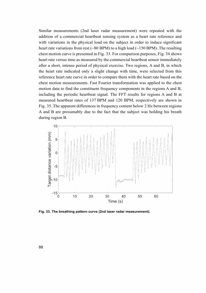
88
Similar measurements (2nd laser radar measurement) were repeated with the
addition of a commercial heartbeat sensing system as a heart rate reference and
with variations in the physical load on the subject in order to induce significant
heart rate variations from rest (~80 BPM) to a high load (~150 BPM). The resulting
chest motion curve is presented in Fig. 33. For comparison purposes, Fig. 34 shows
heart rate versus time as measured by the commercial heartbeat sensor immediately
after a short, intense period of physical exercise. Two regions, A and B, in which
the heart rate indicated only a slight change with time, were selected from this
reference heart rate curve in order to compare them with the heart rate based on the
chest motion measurements. Fast Fourier transformation was applied to the chest
motion data to find the constituent frequency components in the regions A and B,
including the periodic heartbeat signal. The FFT results for regions A and B at
measured heartbeat rates of 137 BPM and 120 BPM, respectively are shown in
Fig. 35. The apparent differences in frequency content below 2 Hz between regions
A and B are presumably due to the fact that the subject was holding his breath
during region B.
Fig. 33. The breathing pattern curve (2nd laser radar measurement).
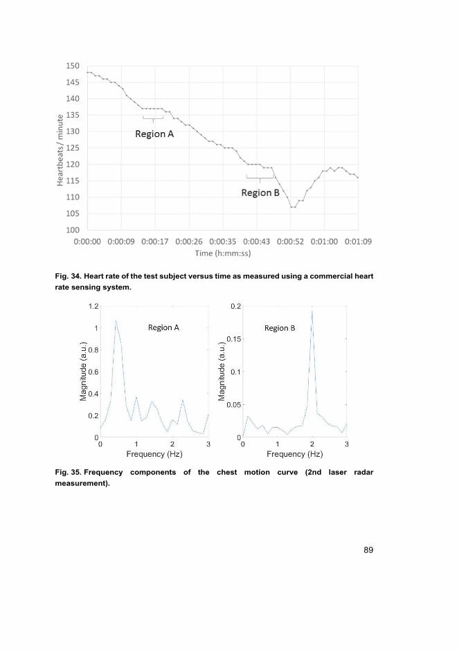
89
Fig. 34. Heart rate of the test subject versus time as measured using a commercial heart
rate sensing system.
Fig. 35. Frequency components of the chest motion curve (2nd laser radar
measurement).
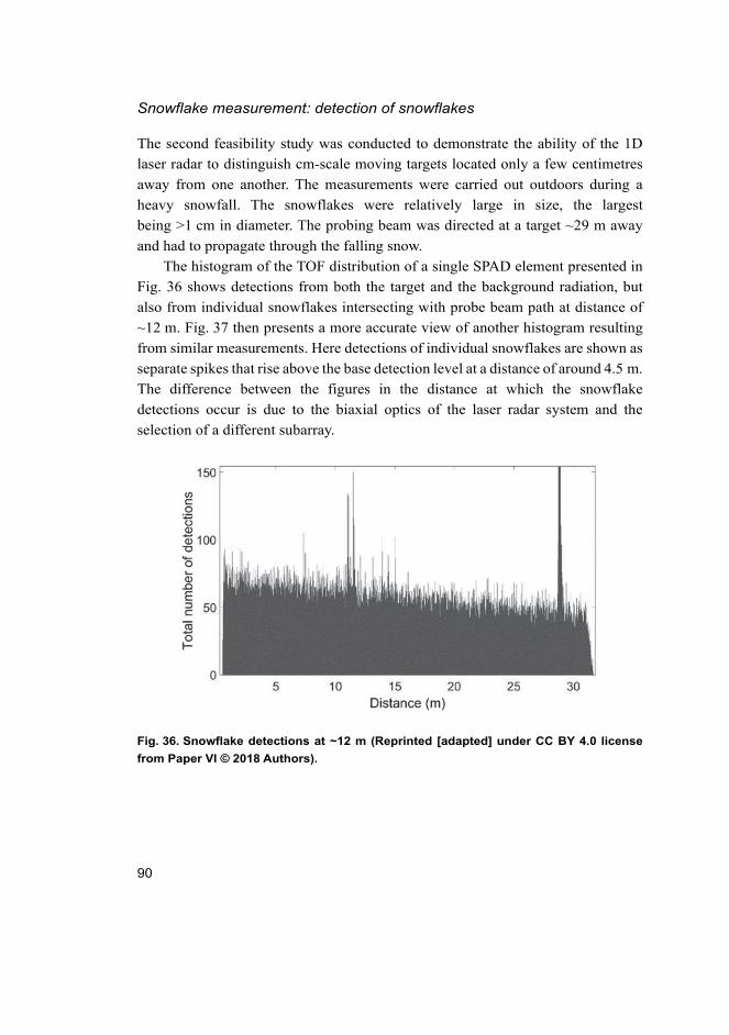
90
Snowflake measurement: detection of snowflakes
The second feasibility study was conducted to demonstrate the ability of the 1D
laser radar to distinguish cm-scale moving targets located only a few centimetres
away from one another. The measurements were carried out outdoors during a
heavy snowfall. The snowflakes were relatively large in size, the largest
being >1 cm in diameter. The probing beam was directed at a target ~29 m away
and had to propagate through the falling snow.
The histogram of the TOF distribution of a single SPAD element presented in
Fig. 36 shows detections from both the target and the background radiation, but
also from individual snowflakes intersecting with probe beam path at distance of
~12 m. Fig. 37 then presents a more accurate view of another histogram resulting
from similar measurements. Here detections of individual snowflakes are shown as
separate spikes that rise above the base detection level at a distance of around 4.5 m.
The difference between the figures in the distance at which the snowflake
detections occur is due to the biaxial optics of the laser radar system and the
selection of a different subarray.
Fig. 36. Snowflake detections at ~12 m (Reprinted [adapted] under CC BY 4.0 license
from Paper VI © 2018 Authors).
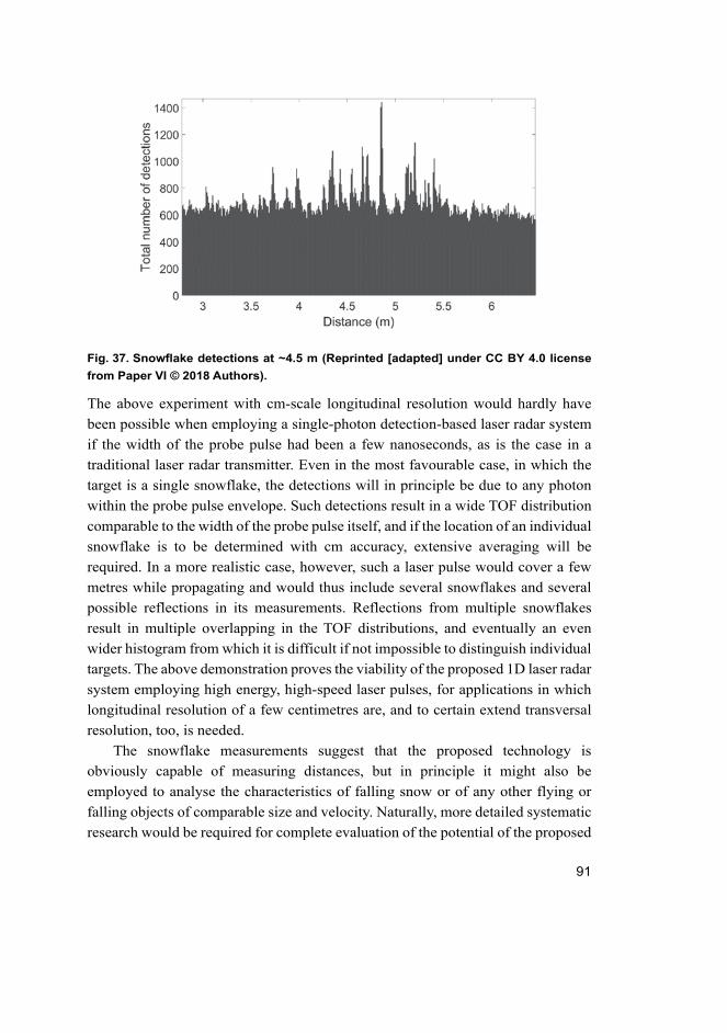
91
Fig. 37. Snowflake detections at ~4.5 m (Reprinted [adapted] under CC BY 4.0 license
from Paper VI © 2018 Authors).
The above experiment with cm-scale longitudinal resolution would hardly have
been possible when employing a single-photon detection-based laser radar system
if the width of the probe pulse had been a few nanoseconds, as is the case in a
traditional laser radar transmitter. Even in the most favourable case, in which the
target is a single snowflake, the detections will in principle be due to any photon
within the probe pulse envelope. Such detections result in a wide TOF distribution
comparable to the width of the probe pulse itself, and if the location of an individual
snowflake is to be determined with cm accuracy, extensive averaging will be
required. In a more realistic case, however, such a laser pulse would cover a few
metres while propagating and would thus include several snowflakes and several
possible reflections in its measurements. Reflections from multiple snowflakes
result in multiple overlapping in the TOF distributions, and eventually an even
wider histogram from which it is difficult if not impossible to distinguish individual
targets. The above demonstration proves the viability of the proposed 1D laser radar
system employing high energy, high-speed laser pulses, for applications in which
longitudinal resolution of a few centimetres are, and to certain extend transversal
resolution, too, is needed.
The snowflake measurements suggest that the proposed technology is
obviously capable of measuring distances, but in principle it might also be
employed to analyse the characteristics of falling snow or of any other flying or
falling objects of comparable size and velocity. Naturally, more detailed systematic
research would be required for complete evaluation of the potential of the proposed

92
technology for producing such measurements. Nevertheless, the preliminary results
look interesting.
93
7 Discussion
The goal of the present research was to study the performance and design principles
of a 1D laser radar system employing a 2D SPAD detector array in conjunction
with a high-speed (sub-nanosecond FWHM), high energy (~1 nJ) laser pulse. The
design rests upon the known theory of SPAD-based single-photon detection
(Fouche, 2003; Henriksson, 2005) and it is intended for as a proposition for a
system construction of a 1D laser radar implementation for industrial applications
up to ~100 m range. The emphasis of the design was on system-level performance
and, importantly, compact system integration. An actual 1D laser radar system was
implemented in order to test and verify the proposed design principles by studying
its system-level performance and the features actualized by the detector array
configuration. Based on a survey of the extensive literature concerning SPAD-
based laser radar research, as reviewed briefly in section 2.7, the present research
is among the first successful attempts to design and implement a miniaturized high
performance 1D laser radar device combining the above technologies.
The first part of this research was concerned with the preliminary
characterization of two types of laser diode in order to evaluate their applicability
for use in a pulsed TOF laser radar system employing a CMOS SPAD detector. The
custom-developed laser diodes were of the bulk and QW types (stripe width 30 µm,
cavity length 3.0 mm), operating in enhanced gain switching mode. The
characterization measurements implied that both laser diodes worked as expected
and served as viable sources for production of ~1 nJ and 100–200 ps FWHM laser
pulses, thus enabling measurements to be made over distances of several tens of
metres with cm-scale precision (~ms-scale measurement time, receiver aperture
diameter of ~20 mm). Laser diodes with other cavity dimensions were also tested
and the results pointed to differences in performance regarding output power and
driving requirements, thus increasing the variety of available laser pulse sources.
Of the two laser diodes it was the QW type that demonstrated the more
desirable overall performance, particularly due to its lower lasing threshold, which
resulted in a lower dependence of output power on operation temperature, thus
ensuring more stable operation at varying temperatures in practical applications.
The QW laser diode also has a shorter emission wavelength at which the PDE of a
CMOS SPAD increases, thus compensating for the lower output power (a single
isolated pulse) as compared with a bulk laser diode. In general terms, the selection
of the laser pulse source is actually application-specific and depends on the required
94
laser power, power consumption constraints, the spectral dependence of the PDE
and the level of background radiation, for example.
One important feature of a laser diode operating in the enhanced gain switching
regime is that it produces a laser pulse of ~100 ps even though it is driven by a
much wider current pulse (1–2 ns FWHM). The implementation of such a driver is
fairly simple and therefore compact, which is central requirement for a transmitter
from the point of view of system integration. Both laser diodes used in this work
were driven by a current pulser circuit employing a high-speed MOSFET switch
producing a current pulse with an amplitude of 10–15 A and FWHM of ~1.5 ns.
Pulsing rates of up to 1 MHz were demonstrated, but beyond this the laser output
power decreased significantly due to excess heating of the driver electronics, so
that active cooling would have been required for optimal output. Thus a pulsing
rate of 100 kHz could be used in the actual 1D laser radar implementation with no
severe heating problem.
The commercially available laser diodes that operate in conventional gain
switching mode, as typically used in single-photon detection laser radars, generate
~100 ps laser pulses but with significantly lower energy than the laser diodes
studied here. Although the average optical power may be partially compensated for
by increasing the pulsing rate, it is important to note that a high energy probe pulse
is of value in itself in pulsed TOF laser radar applications and its absence cannot
be straightforwardly compensated for by a higher pulsing rate. Higher pulsing rates
will increase not only the signal detection rate but also the noise detection rate,
which will partially cancel out the increase in the signal detection rate. This
cancelling effect becomes particularly evident under measurement conditions
involving high-level background radiation.
GaN transistor technology has proved a viable alternative to a laser driver
switch due to its superior switching speed and heat dissipation and might well
become the switch of choice in compact laser diode drivers in the near future. Our
recent laser transmitter studies have demonstrated the availability of even more
energetic laser pulses (~10 nJ, ~130 ps FWHM) when using a bulk laser diode
operating in enhanced gain switching mode (stripe width 90 µm, cavity length
3.0 mm) driven by a GaN current pulser. The increase in probe pulse energy is
desirable in itself from the SNR point of view, but the associated three-fold increase
of stripe width is potentially adverse since the receiver FOV needs to be three times
greater, too, for efficient signal reception. In the presence of background radiation,
this means nine times greater background power reception, which will partially
cancel out the advantageous effect of the increased probe pulse energy on the SNR.
95
The second part of the research dealt with the design, implementation and
characterization of a 1D laser radar system employing the above QW laser diode
and a CMOS receiver IC containing a 2D SPAD array and a multi-channel TDC. A
laser radar system was implemented in order to study the system-level performance
of such a technology and the features actualized by the employment of a detector
array configuration in a 1D SPAD laser radar device. The total energy of the probe
pulse was 0.6 nJ and the diameter of the circular receiver aperture ~20 mm,
whereupon the pulsing rate was 100 kHz. The results of the characterization
measurements were: walk error ~5 cm (dynamic range ~1:100 000), linearity
±0.5 mm, signal detection rate ~28% (target distance 34 m and reflectivity 11%)
and precision ~2 cm. Comparison with the single-photon detection techniques
presented in the literature review chapter, showed the most distinct difference to
exist in the case of the system presented by Buller et al. (2012), which has an order
of magnitude better precision, due to the <1 ps laser pulse width and superior IRF
(~10 ps) of the SNSPD detector. The overall performance was nevertheless
comparable to that of the state-of-the-art linear detection radar described by Kurtti
et al. (2019).
As pointed out, the detector for the system was realized as a 2D array (9x9) of
SPAD detector elements, within which any of the 3x3 sub-arrays could be
electrically selected for photon detection. One of the central features of the system
is that each of the nine subarray elements has an exclusive TDC channel, enabling
multiple parallel measurement results for each single probe pulse. The key
advantage of this approach is that it simultaneously enables the use of a large
detector surface and the achievement of a small effective FOV in the detector. A
large surface is needed since the received laser spot moves laterally across the
detector surface along with the target distance (biaxial optics). In addition,
activation of only those detector elements which are actually detecting probe pulse
photons ensures that the effective FOV of the receiver remains small, which is
important for reducing the effect of background radiation-induced noise. Another
advantageous feature of this approach is that in principle it permits walk error-free
measurements. Due to the 2D detector array configuration with a selectable
subarray feature and the distribution of the laser spot energy over several SPAD
elements, it is possible to select a subarray containing mainly those detector
elements that are operating in or close to single-photon detection mode even when
the total received energy is high. By contrast, walk error compensation in linear
mode detection technologies, as well as with the analogue SiPM, requires post-
processing of the measurement data, thus increasing the complexity of the system.

96
In single-photon detection, the proposed walk error compensation methods
presented in the literature review demonstrate promising results, but either suffer
from limited dynamic range (up to the maximum detection rate of 100%) or
increases the complexity of the system (an APD detector in addition to analog
receiver channel).
Another means of reducing the effect of background photon-induced noise in
the laser radar system developed here was seen to be detector time gating. Time
gating measurements carried out outdoors under conditions of high-level
background radiation (~90 klx) demonstrated a significant reduction in the number
of background photon detections and thus an improvement in the signal detection
rate (a ~500-fold increase with the target at 34 m), a higher measurement speed and
greater precision, as well as the prevention of total detector blockage by photons
from background radiation. Another benefit of photon coincidence detection in
addition to decreased data load of the system is, that it can be used to reduce
background radiation induced false detections as presented in the literature review.
This method, however, relies heavily on powerful transmitter, which imposes
constraints related to the system performance and implementation, and improved
tolerance to higher background radiation levels comes at the expense of reduced
sensitivity at low signal levels.
The feasibility studies carried out here showed the laser radar system to achieve
high spatial accuracy when measuring the heart rate of a human subject at a distance
of 4 m with cm-precision, which in conjunction with high-speed averaging could
result in sub-mm accuracy. The system was also used to detect individual
free-falling snowflakes during a snowfall, this being attributed to the cm-scale
precision of the device, its low beam divergence and the ability of the SPAD
detector to distinguish multiple echoes in a longitudinal direction.
The implementation and characterization of this laser radar system employing
a custom-made laser diode producing high energy, high-speed laser pulses and a
2D CMOS SPAD array detector demonstrated the viability of the proposed
technology for high performance distance measurement and, importantly, for
compact realization. The moderate overall physical size of the system, due to its
simple transmitter and single-chip receiver IC, is a highly desirable feature
endowing the technology with a potential for use in a variety of applications. The
compact overall size of the system is one of its key advantages relative to the other
single-photon detection laser radar techniques presented in the literature review. In
addition, the SPAD-based “digital” receiver appears to be virtually immune to EMI
even in the proximity (~2 cm) of laser transmitter producing interference due to the
97
high current transient of the laser pumping. This non-susceptibility to
electromagnetic interference is good news for prospective emerging laser radar
systems and applications with high levels of system integration and represents
another advantage of the proposed system in contrast to linear detection techniques
employing a sensitive analogue receiver channel. Commercial FlightSense product
family offers truly compact sized ranging sensors, but ranging performance seems
to scale down as well, rendering them applicable only for short range distance
measurements of few metres.
As for the consideration of whether and under what conditions the SPAD
technique could serve as an alternative to or substitute for linear detection, a brief
comparison should be made between this 1D laser radar system and the state-of-
the-art linear technique employing laser radar. The comparison should be focused
on the key performance parameters and implementation questions at the system and
module levels. The physical implementation of the SPAD receiver is significantly
simpler due to the digital output signal of the SPAD detector element, which
eliminates the need for an interference-prone and technologically demanding
analogue receiver channel, which can also impose limits on the performance of the
receiver. Also, the simplicity of the receiver electronics obviously influences the
design and manufacturing costs, the IC area required, the overall size of the system
etc. A Si SPAD is also CMOS compatible, thus enabling the realization of
application-specific integrated single-chip receiver modules.
From the point of view of the key performance parameters, precision and
accuracy, the two technologies proved to be substantially comparable. The marked
difference, though, was the greater photon sensitivity of a SPAD detector. Greater
photon sensitivity, a highly desirable feature of laser radar applications suffering
from photon scarcity, is simultaneously a major drawback, however, and can lead
to background noise issues and at worst a risk of total detector blockage. This stands
in stark contrast to the linear detection technique, in which background radiation
only increases the detector noise level, thus reducing the SNR but without any total
blocking of the detector. The detection time gate feature proved to be an effective
means of suppressing the background noise in conjunction with the SPAD
technique, although effective time gating requires a prior knowledge of the target
distance, which in turn prolongs the measurement time, or calls for the use of more
sophisticated detector configurations and time gating algorithms. Another
difference, also resulting from the deviant natures of the detectors, is that linear
detection has true single-shot precision, whereas in SPAD detection an individual
measurement is ultimately unreliable due to the risk of false detections. Therefore

98
a reliable result requires statistical sampling, which will increase the measuring
time and, in addition to the rather low PDE of a Si SPAD, will effectively narrow
the sensitivity gap between the detectors.
99
8 Summary
The automation of modern life and societies is generating an increasing need for a
variety of autonomous environment perception systems. Laser radar has proved to
be a potential alternative in the field of distance sensor technology in fields such as
driver-assisted cars and robotics, for example. The key performance parameters
required from these systems are centimetre-scale or better measurement accuracy,
a measurement range of several tens of metres and sub-second measurement time.
Other important practical requirements are compact overall size of the system and
cost-effective implementation.
The conventional solution for constructing a 1D laser radar system based on
the pulsed TOF operation principle employs linear detection techniques, typically
an APD detector and an analogue receiver channel to detect optical echoes and to
determine the timing for the termination of TOF measurement. Linear detection
techniques have now reached their maturity and their characteristics are well known.
They do indeed enable high performance distance measurement, but the analogue
receiver channel and walk error compensation increase the complexity of the
system, thus leaving room for receiver optimization. Another emerging detector
technology is that which employs a silicon SPAD-based single-photon technique.
The key features of a SPAD detector are high photon sensitivity and relaxed
receiver channel specifications, since the absorption of an individual photon may
induce a readily detectable digital-like output signal that indicates the timing of
photon detection with high precision. Photon sensitivity is a highly desirable
feature in laser radar applications characterized by photon scarcity, and the digital
output of the detector allows the receiver electronics to be significantly simpler
than with linear detector techniques. Silicon SPADs are also CMOS-compatible,
thus enabling compact and cost-effective receiver implementations.
The goal of the present research was to design, implement and characterize a
compact 1D laser radar system combining CMOS SPAD detector technology with
a custom-made laser diode, in order to study its performance and characteristics
and to evaluate its viability in practical 1D laser radar applications. Two types of
custom-made laser diode (QW and bulk), operating in enhanced gain switching
mode, were characterized in order to select one to be employed in the laser radar
system. Among the key findings was the discovery that the custom-made bulk and
QW laser diodes both produced isolated high-speed (~100 ps FWHM) laser pulses
with high energy (>1 nJ) when driven by a fairly simple, compact current pulser at
pulsing rates greater than 100 kHz. Also, thanks to its internal operation mechanism
100
the enhanced gain switching mode produced high-speed, high energy laser pulses
with significantly more relaxed current pulse characteristics (amplitude <10 A,
pulse width 1–2 ns FWHM). This stands in stark contrast to the situation in the
conventional gain switching mode, where a complex high-speed driver was
required to production energetic, isolated ~100 ps (FWHM) laser pulses. Obviously
a simple, compact current driver is a desirable feature from the system integration
point of view, but the decisive difference between the bulk and QW laser diodes
was that the output power of the latter proved to be less sensitive to variations in
operating temperature, and it was for this reason that QW diodes were chosen for
use in the actual proto setup for a compact 1D laser radar system.
The system was based on the pulsed TOF operation principle and employed a
2D CMOS SPAD detector array with an exclusive TDC channel for each SPAD
element (a novel feature proposed in this work) and a laser diode producing high
energy (~1 nJ), high-speed (~100 ps FWHM) laser pulses. Optimizations of several
parameters and features were addressed in the design principles for the 1D laser
radar system. In the receiver, a 2D 9x9 array of small (24 µm x 24 µm) SPAD
elements accounted for the moderately low DCR (kHz range) and enabled target
distance-dependent laser spot wandering on the detector surface (biaxial optics).
Moreover, the 2D SPAD array, along with the selectable 3x3 subarray feature,
enabled laser spot tracking while maintaining a small effective FOV in the detector.
This latter feature is important, since it effectively reduces the background
radiation-induced noise, thus partially preventing detector masking and blocking
effects. The receiver also uses detection time gating to reduce the detector blockage
effect.
In order to maximize the signal to background rate (SBR), high pulse energy
was preferred over pulsing frequency, since increasing the latter in the presence of
background radiation would have also increased the number of noise-induced false
detections. Based on theoretical estimates, the energy of the laser pulse (~1 nJ)
should be sufficient for measuring distances of up to several tens of metres at a
detection rate of >20% and with a receiver aperture diameter of ~20 mm in the case
of a low reflectance target. The FWHM of ~100 ps matches quite well with the
timing jitter of the CMOS SPAD element (<100 ps) and can be expected to result
in cm-scale distance measurement precision. As for the physical realization of the
receiver module, emphasis was laid on the system integration, so that a single-chip
CMOS receiver including a SPAD detector array and a multi-channel TDC was
employed. The transmitter and receiver electronics were implemented on a single
35 mm x 40 mm PCB.
101
Characterization of the laser radar system demonstrated high performance with
regard to spatial accuracy and measurement speed. The key performance
parameters were inherent timing walk error ~5 cm (dynamic range ~1:100 000),
linearity ±0.5 mm, signal detection rate ~28% (target distance 34 m and reflectivity
11%) and precision ~2 cm. The total energy of a probe pulse was 0.6 nJ and the
diameter of the circular receiver aperture was 18.4 mm. The linearity results
demonstrated the availability of walk error-free distance measurements enabled by
the selectable subarray feature, while the detector time gating feature proved to be
an effective means of reducing interference from background photon-induced noise
under high-level background radiation conditions (~90 klx). The signal detection
rate increased ~500-fold upon the employment of an optimized time gate. Two
feasibility studies carried out in practical measurement settings demonstrated high
spatial accuracy of the laser radar system in measuring heartbeats from the chest of
a test subject (sub-mm accuracy) and in distinguishing individual falling
snowflakes in a heavy snowfall.

102

103
List of references
Albota, M. A., Aull, B. F., Fouche, D. G., Heinrichs, R. M., Kocher, D. G., Marino, R. M., Mooney, J. G., Newbury, N. R., O’Brien, M. E., Player, B. E., Willard, B. C., & Zayhowski, J. J. (2002). Three-dimensional imaging laser radar with a photon-counting avalanche photodiode array and microchip laser. Applied Optics, 41, 7671–7678.
Amann, M.-C., Bosch, T., Lescure, M., Myllylae, R. & Rioux, M. (2001). Laser ranging: a critical review of usual techniques for distance measurement. Optical Engineering, 40, 10–19.
Baharmast, A., Kurtti, S. & Kostamovaara, J. (2020). A Wide Dynamic Range Laser Radar Receiver Based on Input Pulse-Shaping Techniques. IEEE Transactions on Circuits and Systems I: Regular Papers, 67(8), 2566–2577.
Beer, M., Haase, J. F., Ruskowski, J., & Kokozinski, R. (2018). Background Light Rejection in SPAD-Based LiDAR Sensors by Adaptive Photon Coincidence Detection. Sensors, 18(12), 4338.
Bertolini, G. (1968). Pulse shape and time resolution. In G. Bertolini, & A. Coche (Eds.) Semiconductor Detectors. Amsterdam: North-Holland Publishing.
Blazej, J., & Prochazka, I. (2009). Single and few photon avalanche photodiode detection process study. In K. Zhang, X. Wang, G. Zhang, & K. Ai (Eds.), Proceedings of SPIE: Vol. 7384. International Symposium on Photoelectronic Detection and Imaging 2009: Advances in Imaging Detectors and Applications. SPIE. https://doi.org/10.1117/12.835564
Bronzi, D., Villa, F., Tisa, S., Tosi, A., Zappa, F., Durini, D. Weyers, S., & Brockherde, W. (2014). 100 000 Frames/s 64 × 32 Single-Photon Detector Array for 2-D Imaging and 3-D Ranging. IEEE Journal of Selected Topics in Quantum Electronics, 20(6), 354–363. https://doi.org/10.1109/jstqe.2014.2341562
Buller, G. S., McCarthy, A., Ren, X., Gemmell, N. R., Collins, R. J., Krichel, N. J., Tanner, M. G., Wallace, A. M., Dorenbos, S., Zwiller, V. & Hadfield, R. H. (2012). Depth imaging at kilometer range using time-correlated single-photon counting at wavelengths of 850 nm and 1560 nm. In H. Mohseni, M. H. Agahi, & M. Razeghi (Eds.), Proceedings of SPIE: Vol. 8460, Biosensing and Nanomedicine V. SPIE. https://doi.org/10.1117/12.965890.
Carmer, D. C., & Peterson, L. M. (1996). Laser radar in robotics. Proceedings of the IEEE, 84(2), 299–320.
Cho, H.-S., Kim, C.-H. & Lee, S.-G. (2014). A High-Sensitivity and Low-Walk Error LADAR Receiver for Military Application. IEEE Transactions on Circuits and Systems I: Regular Papers, 61(10), 3007–3015.
Collis, R. T. H., & Russell, P. B. (1976). Lidar measurement of particles and gases by elastic backscattering and differential absorption. In E. D. Hinkley (Ed.), Topics in Applied Physics: Vol. 14. Laser monitoring of the atmosphere (pp. 71–151). Berlin, Heidelberg: Springer. https://doi.org/10.1007/3-540-07743-X_18
Cova, S., Ghioni, M., Lacaita, A., Samori, C. & Zappa, F. (1996). Avalanche photodiodes and quenching circuits for single-photon detection. Applied Optics, 35(12), 1956–1976.

104
Cova, S., Lacaita, M., Ghioni, M. & Ripamonti, G. (1989). 20-ps timing resolution with single-photon avalanche diodes. Review of Scientific Instruments, 60(6), 1104–1110.
Cova, S., Longoni, A. & Andreoni, A. (1981). Towards picosecond resolution with single‐photon avalanche diodes. Review of Scientific Instruments 52(3), 408–412.
Donati, S. (2004). Electro-Optical Instrumentation: Sensing and Measuring with Lasers. Upper Saddle River, NJ, USA: Prentice-Hall.
Ferdinand Braun Institut. (2020, January 9). Pico- & Nanosecond Pulse Sources [Web page]. Retrieved from https://www.fbh-berlin.de/en/research/photonics/laser-modules/ps-ns-pulse-sources
Forrester, P. A. & Hulme, K. F. (1981). Laser rangefinders. Optical and Quantum Electronics, 13, 259–293.
Fouche, D. G. (2003). Detection and false-alarm probabilities for laser radars that use Geiger-mode detectors. Applied Optics, 42(27), 5388–5398.
Frach, T., Prescher, G., Degenhardt, C., de Gruyter, R., Schmitz, A., & Ballizany, R. (2009). The Digital Silicon Photomultiplier–Principle of Operation and Intrinsic Detector Performance. In 2009 IEEE Nuclear Science Symposium Conference Record (NSS/MIC). (pp. 1959–1965). Piscataway, NJ: IEEE.
Gedcke, D. A., & Williams, C. W. (1968). High resolution time spectroscopy: 1. Scintillation detectors. ORTEC Publication (August 1968).
Grum, F., & Becherer, R. (1979). Optical Radiation Measurements: Vol. 1. Radiometry. New York: Academic Press.
He, W., Sima, B., Chen, Y., Dai, H., Chen, Q., & Gu, G. (2013), A correction method for range walk error in photon counting 3D imaging LIDAR. Optics Communications, 308, 211–217.
Heinzen, D. J. & Wineland, D. J. (1990). Quantum-limited cooling and detection of radio-frequency oscillations by laser-cooled ions. Physical Review A, 42(5), 2977–2994.
Henriksson, M. (2005). Detection probabilities for photon-counting avalanche photodiodes applied to a laser radar system. Applied Optics, 44(24), 5140–5147.
Hong, C., Kim, S.-H., Kim, J.-H. & Park, S. M. (2018). A Linear-Mode LiDAR Sensor Using a Multi-Channel CMOS Transimpedance Amplifier Array. IEEE Sensors Journal, 18(17), 7032–7040.
Jahromi, S. S. (2020). Single photon avalanche detector devices and circuits for miniaturized 3D imagers. In Acta Universitatis Ouluensis: Series C Technica (No. 752). Oulu: University of Oulu.
Jahromi, S., Jansson, J., Nissinen, I., Nissinen, J., & Kostamovaara, J. (2015). A Single Chip Laser Radar Receiver with a 9x9 SPAD Detector Array and a 10-Channel TDC. In Proceedings of the 41st European Solid-State Circuits Conference (pp. 364–367). IEEE. https://doi.org/10.1109/ESSCIRC.2015.7313903
Kasap, S. O. (2001). Optoelectronics & photonics: Principles and practices (1st ed.). Upper Saddle River, NJ: Prentice-Hall Inc.
Keränen, P. & Kostamovaara, J. (2019). 256×8 SPAD Array With 256 Column TDCs for a Line Profiling Laser Radar. IEEE Transactions on Circuits and Systems I: Regular Papers, 66(11), 4122–4133.
105
Koskinen, M., Kostamovaara, J. & Myllylae, R. (1992). Comparison of continuous-wave and pulsed time-of-flight laser range-finding techniques. In D. J. Svetkoff (Ed.), Proceedings of SPIE: Vol. 1614. Optics, Illumination, and Image Sensing for Machine Vision VI. SPIE. https://doi.org/10.1117/12.57989
Kostamovaara, J., Jahromi, S. S. & Keränen, P. (2020). Temporal and Spatial Focusing in SPAD-Based Solid-State Pulsed Time-of-Flight Laser. Sensors, 20(21), 5973.
Kostamovaara, J., Nissinen, J., Kurtti, S., Nissinen, I., Jansson, J. & Mäntyniemi, A. (2009). On the Minimization of Timing Walk in Industrial Pulsed Time-of-Flight Laser Radars. In F. Baldini, J. Homola, & R. A. Lieberman (Eds.), Proceedings of SPIE: Vol. 7356. Optical Sensors 2009. SPIE. https://doi.org/10.1117/12.820444
Kurtti, S. & Kostamovaara, J. (2011). An Integrated Laser Radar Receiver Channel Utilizing a Time-Domain Walk Error Compensation Scheme. IEEE Transactions on Instrumentation and Measurement, 60(1), 146–157.
Kurtti, S. (2012). Integrated receiver channel and timing discrimination circuits for a pulsed time-of-flight laser rangefinder. In Acta Universitatis Ouluensis: Series C Technica (No. 439). Oulu: University of Oulu.
Kurtti, S., Jansson, J.-P. & Kostamovaara, J. (2019). A CMOS Receiver–TDC Chip Set for Accurate Pulsed TOF Laser Ranging. IEEE Transactions on Instrumentation and Measurement, 69(5), 2208–2217.
Lanz, B. (2016). Compact current pulse-pumped GaAs–AlGaAs laser diode structures for generating high peak-power (1–50 watt) picosecond-range single optical pulses. In Acta Universitatis Ouluensis: Series C Technica (No. 583). Oulu: University of Oulu.
Lanz, B., Ryvkin, B. S., Avrutin, E. A., & Kostamovaara, J. T. (2013). Performance improvement by a saturable absorber in gain-switched asymmetric-waveguide laser diodes. Optics Express, 21(24), 29780–29791.
Lanz, B., Vainshtein, S. & Kostamovaara, J. (2006). High power gain-switched laser diode using a superfast GaAs avalanche transistor for pumping. Applied Physics Letters, 89(8), 081122–081122–3.
Liero, A., Klehr, A., Schwertfeger, S., Hoffman, T. & Heinrich, W. (2010). Laser driver switching 20 A with 2 ns pulse width using GaN. In 2010 IEEE MTT-S International Microwave Symposium (pp. 1110–1113). IEEE.
Massa, J. S., Buller, G. S., Walker, A. C., Cova, S., Umasuthan, M. & Wallace, A. M. (1998). Time-of-flight optical ranging system based on time-correlated single-photon counting. Applied Optics, 37(31), 7298–7304.
McCarthy, A., Collins, R. J., Krichel, N. J., Fernández, V., Wallace, A. M. & Buller, G. S. (2009). Long-range time-of-flight scanning sensor based on high-speed time-correlated single-photon counting. Applied Optics, 48(32), 6241–6251.
McCarthy, A., Ren, X., Della Frera, A., Gemmell, N. R., Krichel, N. J., Scarcella, C., Ruggeri, A., Tosi, A. & Buller, G. S. (2013). Kilometer-range depth imaging at 1550 nm wavelength using an InGaAs/InP single-photon avalanche diode detector. Optics Express, 21(19), 22098–22113.
McIntyre, R. J. (1970). Comparison of photomultipliers and avalanche photodiodes for laser applications. IEEE Transactions on Electron Devices, 17(4), 347–352.

106
McManamon, P. F., Banks, P., Beck, J., Fried, D. G., Huntington, A. S. & Watson, E. A. (2017). Comparison of flash lidar detector options. Optical Engineering, 56(3), 031223.
Muoi, T. (1984). Receiver design for high-speed optical-fiber systems. Journal of Lightwave Technology, 2(3), 243–267.
Neville, A. M. & Kennedy, J. B. (1964). Basic statistical methods for engineers and scientists. London, UK: Intertext Books.
Niclass, C., Rochas, A., Besse, P.-A. & Charbon, E. (2005). Design and Characterization of a CMOS 3-D Image Sensor Based on Single Photon Avalanche Diodes. IEEE Journal of Solid-State Circuits, 40(9), 1847–1854.
Niclass, C., Soga, M., Matsubara, H., Kato, S. & Kagami, M. (2013). A 100-m Range 10-Frame/s 340 × 96-Pixel Time-of-Flight Depth Sensor in 0.18-μm CMOS. IEEE Journal of Solid-State Circuits, 48(2), 559–572.
Nissinen, J. & Kostamovaara, J. (2013). A 4 A peak current and 2 ns pulse width CMOS laser diode driver for high measurement rate applications. In 2013 Proceedings of the ESSCIRC (ESSCIRC). https://doi.org/10.1109/esscirc.2013.6649146
Nissinen, J. (2011). Integrated CMOS circuits for laser radar transceivers. In Acta Universitatis Ouluensis: Series C Technica (No. 389). Oulu: University of Oulu.
Pancheri, L. & Stoppa, D. (2007). Low-Noise CMOS single-photon avalanche diodes with 32 ns dead time. In Proceedings of the 37th European Solid State Device Research Conference (ESSDERC) (362–365). Piscataway, NJ: IEEE. https://doi.org/10.1109/essderc.2007.4430953
Pedrotti, F. L. & Pedrotti, L. S. (1993). Introduction to Optics (2nd ed.). N.J.: Prentice-Hall. Pellegrini, S., Buller, G. S., Smith, J. M., Wallace, A. M. & Cova, S. (2000). Laser-based
distance measurement using picosecond resolution time-correlated single-photon counting. Measurement Science and Technology, 11(6), 712–716.
Pellegrini, S. & Rae, B. (2017). Fully industrialised single photon avalanche diodes. In M. A. Itzler & J. C. Campbell (Eds.), Proceedings of SPIE: Vol. 10212. Advanced Photon Counting Techniques XI. SPIE. https://doi.org/10.1117/12.2264364 10212.
Perenzoni, M., Perenzoni, D., & Stoppa, D. (2016). A 64×64-Pixels Digital Silicon Photomultiplier Direct TOF Sensor With 100-MPhotons/s/pixel Background Rejection and Imaging/Altimeter Mode With 0.14% Precision Up To 6 km for Spacecraft Navigation and Landing. IEEE Journal of Solid-State Circuits, 52(1), 151–160.
Pfennigbauer, M. & Ullrich, A. (2007). Applicability of single photon detection for laser radar. Elektrotechnik und Informationstechnik, 124(6), 180–185.
PicoQuant. Picosecond Pulsed Sources [Web page]. Retrived from https://www.picoquant.com/products/category/picosecond-pulsed-sources
Renker, D. (2006). Geiger-mode avalanche photodiodes, history, properties and problems. Nuclear Instruments and Methods in Physics Research, 567(1), 48–56.
Rieger, P. (2014). Range ambiguity resolution technique applying pulse-position modulation in time-of-flight scanning lidar applications. SPIE Optical Engineering, 53(6), 061614.
107
Rochas, A., Besse, P. A., & Popovic, R. S. (2001). A Geiger Mode Avalanche Photodiode Fabricated in a Conventional CMOS Technology. In Proceedings of the 31st European Solid-State Device Research Conference. IEEE. https://doi.org/10.1109/essderc.2001.195306
Ruokamo, H., Hallman, L. & Kostamovaara, J. (2019). An 80×25 Pixel CMOS Single-Photon Sensor with Flexible On-Chip Time Gating of 40 Subarrays for Solid-State 3-D Range Imaging. IEEE Journal of Solid-State Circuits, 54(2), 501–510.
Ryvkin, B., Avrutin, E. & Kostamovaara, J. (2009). Asymmetric-waveguide laser diode for high-power optical pulse generation by gain switching. IEEE Journal of Lightwave Technology, 27(12), 2125–2131.
Ryvkin, B., Avrutin, E. A. & Kostamovaara, J. (2011). Quantum Well laser with an extremely large active layer width to optical confinement factor ratio for high-energy single picosecond pulse generation by gain switching. Semiconductor Science and Technology, 26(4), 045010.
Samain, E. (1998). Timing of optical pulses by a photodiode in the Geiger mode. Applied Optics, 37(3), 502–506.
STMicroelectronics. LiDAR in a Chip FlightSense™ Introduction to Time of Flight [Presentation]. Retrieved from https://www.st.com/content/ccc/resource/sales_and_marketing/presentation/product_presentation/group0/e0/84/0c/fb/11/ec/49/1d/SensorsLive_LiDAR_Chip/files/SensorsLive_LiDAR_Chip.pdf/jcr:content/translations/en.SensorsLive_LiDAR_Chip.pdf
Svelto, O. (1998). Principles of lasers (4th ed.). New York and London: Plenum Press. Tosi, A., Villa, F., Bronzi, D., Zou, Y., Tamborini, D., Tisa, S., Durini, D., Weyers, S.,
Pashen, U., Brockherde, W. & Zappa, F. (2014). Low-noise CMOS SPAD arrays with in-pixel time-to-digital converters. In M. A. Itzler & J. C. Campbell (Eds.), Proceedings of SPIE: Vol. 9114. Advanced Photon Counting Techniques VIII. SPIE. https://doi.org/10.1117/12.2053415
Vainshtein, S. N., Yuferev, V. S. & Kostamovaara J. T. (2002). Properties of the Transient of Avalanche Transistor Switching at Extreme Current Densities. IEEE Transactions on Electron Devices, 49(1), 142–149.
Vainshtein, S. N., Yuferev, V. S. & Kostamovaara, J. T. (2003). Avalanche transistor operation at extreme currents: physical reasons for low residual voltages. Solid-State Electronics, 47, 1255–1263.
Wallace, A. M., Buller, G. S. & Walker, A. C. (2001). 3D imaging and ranging by time-correlated single photon counting. Computing and Control Engineering, 12(4), 157–168.
Wang, J. & Kostamovaara, J. (1994). Radiometric analysis and simulation of signal power function in a short-range laser radar. Applied Optics, 33(18), 4069–4076.
Wojtanowski, J., Zygmunt, M., Kaszczuk, M., Mierczyk, Z. & Muzal, M. (2014). Comparison of 905 nm and 1550 nm semiconductor laser rangefinders’ performance deterioration due to adverse environmental conditions. Opto-Electronics Review, 22(3), 183–190.

108
Zappa, F., Tisa, S., Tosi, A. & Cova, S. (2007). Principles and features of single-photon avalanche diode arrays. Sensors and Actuators A 140, 103–112.
Zhang, C., Lindner, S., Antolovic, I. M., Pavia, J. M., Wolf, M. & Charbon, E. (2019). A 30-frames/s, 252×144 SPAD Flash LiDAR with 1728 Dual-Clock 48.8-ps TDCs, and Pixel-Wise Integrated Histogramming. IEEE Journal of Solid-State Circuits, 54(4), 1137–1151.
Zheng, H., Ma, R., Liu, M. & Zhu, Z. (2019). A Linear-Array Receiver Analog Front-End Circuit for Rotating Scanner LiDAR Application. IEEE Sensors Journal, 19(13), 5053–5061.
109
Original publications
I Hallman, L., Huikari, J., & Kostamovaara, J. (2014). A high-speed/power laser transmitter for single photon imaging applications. In IEEE Sensors 2014 Proceedings. IEEE. https://doi.org/10.1109/icsens.2014.6985213
II Huikari, J. M. T., Avrutin, E. A., Ryvkin, B. S., Nissinen, J. J., & Kostamovaara, J. T. (2015). High-energy picosecond pulse generation by gain switching in asymmetric waveguide structure multiple quantum well lasers. IEEE Journal of Selected Topics in Quantum Electronics, 21(6), 1501206. https://doi.org/10.1109/jstqe.2015.2416342
III Kostamovaara, J., Huikari, J., Hallman, L., Nissinen, I., Nissinen, J., Rapakko, H., Avrutin, E., & Ryvkin, B. (2015). On laser ranging based on high-speed/energy laser diode pulses and single-photon detection techniques. IEEE Photonics Journal, 7(2), 7800215. https://doi.org/10.1109/jphot.2015.2402129
IV Huikari, J., Avrutin, E., Ryvkin, B., & Kostamovaara, J. (2016). High-energy sub-nanosecond optical pulse generation with a semiconductor laser diode for pulsed TOF laser ranging utilizing the single photon detection approach. Optical Review, 23, 522–528. https://doi.org/10.1007/s10043-016-0189-7
V Huikari, J., Jahromi, S., Jansson, J.-P., & Kostamovaara, J. (2017). A laser radar based on a “Impulse-like” laser diode transmitter and a 2D SPAD/TDC receiver. In 2017 IEEE International Instrumentation and Measurement Technology Conference (I2MTC). IEEE. https://doi.org/10.1109/i2mtc.2017.7969799
VI Huikari, J., Jahromi, S., Jansson, J.-P., & Kostamovaara, J. (2018). Compact laser radar based on a subnanosecond laser diode transmitter and a two-dimensional CMOS single-photon receiver. Optical Engineering, 57(2), 024104. https://doi.org/10.1117/1.oe.57.2.024104
Reprinted with permission from IEEE (Papers I, II, III and V © 2014, 2015, 2017
IEEE) and under CC BY 4.0 license1 (Paper IV and VI © 2016, 2018 Authors).
Original publications are not included in the electronic version of the dissertation.
1 https://creativecommons.org/licenses/by/4.0/

110

A C T A U N I V E R S I T A T I S O U L U E N S I S
Book orders:Virtual book store
http://verkkokauppa.juvenesprint.fi
S E R I E S C T E C H N I C A
782. Kekkonen, Jere (2021) Performance of a 16×256 time-resolved CMOS single-photon avalanche diode line sensor in Raman spectroscopy applications
783. Borovkova, Mariia (2021) Polarization and terahertz imaging for functionalcharacterization of biological tissues
784. de Castro Tomé, Mauricio (2021) Advanced electricity metering based on event-driven approaches
785. Järvenpää, Esko (2021) Yläpuolisen siltakaaren optimaalinen muoto
786. Lindholm, Maria (2021) Insights into undesired load factors at work now andtomorrow : findings from different professions and working conditions
787. Miettinen, Jyrki & Visuri, Ville-Valtteri & Fabritius, Timo (2021) Carbon-containingthermodynamic descriptions of the Fe–Cr–Cu–Mo–Ni–C system for modelingthe solidification of steels
788. Tavakolian, Mohammad (2021) Efficient spatiotemporal representation learningfor pain intensity estimation from facial expressions
789. Longi, Henna (2021) Regional innovation systems and company engagement in theArctic context
790. Moltafet, Mohammad (2021) Information freshness in wireless networks
791. Nevanperä, Tuomas (2021) Catalytic oxidation of harmful chlorine- and sulphur-containing VOC emissions : a study of supported Au, Pt and Cu catalysts
792. Baharmast, Aram (2021) Wide dynamic range CMOS receiver techniques for apulsed Time-of-Flight laser rangefinder
793. Haiko, Oskari (2021) Effect of microstructural characteristics and mechanicalproperties on the impact-abrasive and abrasive wear resistance of ultra-highstrength steels
794. Oppenlaender, Jonas (2021) Crowdsourcing creative work
795. Kimbi Yaah, Velma Beri (2021) Development of novel biomass-based materialsfor the treatment of emerging contaminants in water
796. Liu, Chen-Feng (2021) Resource allocation for ultra-reliable and low-latency 5Gcommunication
797. Kilpijärvi, Joni (2021) RF-microwave sensor development for cell and human invitro and ex vivo monitoring
C798etukansi.fm Page 2 Tuesday, August 17, 2021 2:59 PM

UNIVERSITY OF OULU P .O. Box 8000 F I -90014 UNIVERSITY OF OULU FINLAND
A C T A U N I V E R S I T A T I S O U L U E N S I S
University Lecturer Tuomo Glumoff
University Lecturer Santeri Palviainen
Postdoctoral researcher Jani Peräntie
University Lecturer Anne Tuomisto
University Lecturer Veli-Matti Ulvinen
Planning Director Pertti Tikkanen
Professor Jari Juga
Associate Professor (tenure) Anu Soikkeli
University Lecturer Santeri Palviainen
Publications Editor Kirsti Nurkkala
ISBN 978-952-62-3035-1 (Paperback)ISBN 978-952-62-3036-8 (PDF)ISSN 0355-3213 (Print)ISSN 1796-2226 (Online)
U N I V E R S I TAT I S O U L U E N S I SACTAC
TECHNICA
U N I V E R S I TAT I S O U L U E N S I SACTAC
TECHNICA
OULU 2021
C 798
Jaakko Huikari
2D CMOS SPAD ARRAY TECHNIQUES IN 1D PULSED TOF DISTANCE MEASUREMENT APPLICATIONS
UNIVERSITY OF OULU GRADUATE SCHOOL;UNIVERSITY OF OULU,FACULTY OF INFORMATION TECHNOLOGY AND ELECTRICAL ENGINEERING
C 798
AC
TAJaakko H
uikariC798etukansi.fm Page 1 Tuesday, August 17, 2021 2:59 PM