c a ta l o g 2017
TRANSCRIPT

GaN Solutionsatyourfingertips
Sequencers,C ontrollers,and Sw itchesforGaN Transistors
C A TA L O G 2017

INDEX PAGE
100X, 100L, 100T Series Controllers. Negative Input Bias 1
200X, 200L, 200T Series Controllers. Positive Input Bias 3
300PNC Series CMOS Power Switches 4
400X, 400L, 400T Series Dual MOS Mini Switches 7
600E Series Evaluation Boards. Compact, Drop-In 9
700E Series Evaluation Boards. Removable Modules 11
XAN-2 App Note. Connecting Controller & Switch 12
XAN-4 App Note. Mounting Schemes for the Controller 19
XAN-6 App Note. Converting Switch from Pulsed to CW 21
To our valued customers
Thank you for your interest in XSYSTOR products. We make peripheral cir-
cuits for the GaN device. They are sequencers, controllers, modulators, and
switches that are frequency neutral and can operate devices in L, S, C, X, Ku &
Ka-bands. We offer solutions for Broadband Amplifiers, Radar, Milcom, Sat-
com, Point-to-point radio, and Telecom. In addition to our standard products,
our principals have 25 years of RF/Microwave amplifier design experience to
offer custom products as well.
A Q uick S um m ary of ourP rod ucts… ...Electrical Benefits of the Controller
It is a sequencer. The primary job is to protect the GaN device from anyorder of supply and signal voltage turn-ON.
It stabilizes the transistor. GaN maybe superior but it has a flaw; a ten-dency to oscillate at low voltages. To avoid instability when ramping orpulsing the drain, the gate is allowed to switch ON & OFF ONLY if drainvoltage has reached a safe level. It just takes one TTL enable to activate.
Operate your GaN from either gate or drain. They have independentcontrol, so you choose based on your application or preference.
It’s a modulator. You can do pulse-width modulation with the gate ordynamic envelope switching with the drain.
Got Negative? No matter. A single power supply is all that’s needed.Onboard inverter produces -4.3V at 30mA. If not enough, then attachanother negative source and boost to -6V at 100mA.
One for all, and all for one! A single controller can switch several GaNdevices at once, with about 200mA of total switch loads. However, useop-amp or LDO buffers at each gate for best results.
Very fast! It can do <<200 nsec Rise, Fall, or Propagation times whenused together with our power CMOS Switch products.
Mechanical Benefits of the Controller
Half the size of a nickel? At ¼ square inch, it can fit in the most demand-ing footprint and height restriction. Mount it upright, slanted, or flat.
Place it anywhere, any direction. Unlike our competitors, our in-line,castellated port design makes it possible to orientate the module 360°with no printed line crossover.
Applicaon Checklist S tartdesignhere
S ystem R equirem ents
10
0C
on
trollers
20
0C
on
trollers
30
0Sw
itche
s
60
0/
70
0EvalB
oard
I prefer to use negave analog inputforgatebias
I prefer to use posive analog inputforgatebias
Ionly haveonepow ersupplyavailabletothetransistor
100X 200X
I have an addional negave supply available
122X 222X
I can provide negave and logic suppliesalso
124X 224X
Ineedbothdrainandgatedynam icsw itching
100X 200X
Idonotneedgatesw itching120X122X124X
220X222X224X
O verallheightm ustbelessthan0.25” [6.35m m ]
100L 200L
I w ant to lay the m odule fl at dow nto0.10” [2.54m m ]height
100X 200X
M y transistor has CW operaon or> 5m secperiod
M y transistorhasP ulsedopera-on at < 5m sec period w ith typi-calpulsew idthupto500usec
332P362P392P
IhaveR ise/FallT im erequire-m entsof200nsec& propaga-on m e of 200nsec in pulsed m ode
335CT365CT395CT
I w ant to use m ulple sw itches w ithjustonecontroller
I don’t have m e to put every-thingtogether.Ijustw anttodrop-in the w hole soluon next tom y GaN testboard
610E620E630E640E
Givem eyourfastestcontrollerandsw itchtoevaluate.T henIw anttorem oveandreusethem odules for a real applicaon
735E765E795E
11331 E. 183rd STREET # 209, CERRITOS CA 90703, PHONE/FAX: 888-968-7755, EMAIL: [email protected], WWW.XSYSTOR.COM
P RO D UC T FL YERN ovem ber2016
General Descripon
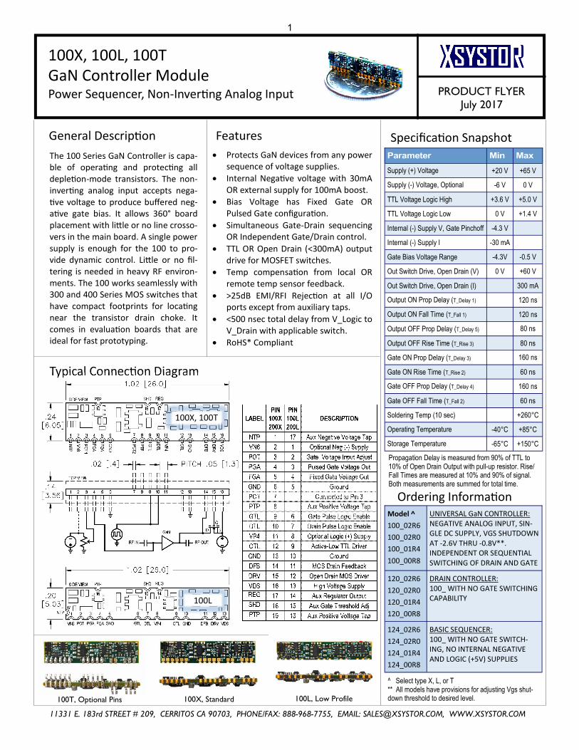
T he100 S eriesGaN Controlleriscapa-ble of operang and protecng all depleon-m ode transistors.T he non-inverng analog input accepts nega-ve voltage to produce buffered neg-ave gate bias. It allow s 360° board placem ent w ith li le or no line crosso-versinthem ainboard.A singlepow ersupply isenough forthe 100 to pro-vide dynam ic control. L i le or no fi l-tering isneeded in heavy R F environ-m ents.T he100 w orksseam lessly w ith300 and 400 S eriesM O S sw itchesthathave com pact footprints for locang near the transistor drain choke. Itcom es in evaluaon boards that are idealforfastprototyping.
100X ,100L ,100TGaN ControllerM oduleP ow erS equencer,N on-Inverng Analog Input
P rotectsGaN devicesfrom any pow ersequenceofvoltagesupplies.
Internal N egave voltage w ith 30m A O R externalsupply for100m A boost.
Bias Voltage has Fixed Gate O RP ulsed Gate confi guraon.
S im ultaneousGate-Drain sequencingO R IndependentGate/Draincontrol.
T T L O R O pen Drain (<300m A)outputdriveforM O S FET sw itches.
T em p com pensaon from local O R rem otetem psensorfeedback.
>25dB EM I/R FI R ejecon at all I/O portsexceptfrom auxiliary taps.
<500 nsectotaldelay from V_L ogictoV_Drainw ithapplicablesw itch.
R oHS * Com pliant
Features S pecifi caon S napshot
Supply (+) Voltage +65 V
Supply (-) Voltage, Optional 0 V
Output ON Fall Time (T_Fall 1) 120 ns
Output OFF Prop Delay (T_Delay 5) 80 ns
TTL Voltage Logic High +5.0 V
Output ON Prop Delay (T_Delay 1) 120 ns
Internal (-) Supply I
Out Switch Drive, Open Drain (V) +60 V
Out Switch Drive, Open Drain (I) 300 mA
+20 V
-6 V
+3.6 V
-30 mA
0 V
Output OFF Rise Time (T_Rise 3) 80 ns
Gate ON Prop Delay (T_Delay 3) 160 ns
Gate ON Rise Time (T_Rise 2) 60 ns
Gate OFF Prop Delay (T_Delay 4) 160 ns
Gate OFF Fall Time (T_Fall 2) 60 ns
Soldering Temp (10 sec) +260°C
Operating Temperature -40°C +85°C
Storage Temperature -65°C +150°C
Gate Bias Voltage Range -4.3V -0.5 V
Internal (-) Supply V, Gate Pinchoff -4.3 V
TTL Voltage Logic Low 0 V +1.4 V
T ypical Connecon Diagram
O rdering Inform aon
Propagation Delay is measured from 90% of TTL to10% of Open Drain Output with pull-up resistor. Rise/Fall Times are measured at 10% and 90% of signal.Both measurements are summed for total time.
M odel
100_02R 6
100_02R 0
100_01R 4
100_00R 8
U N IVER S AL GaN CO N T R O L L ER :N EGAT IVEAN AL O G IN P U T ,S IN -GL EDC S U P P L Y,VGS S HU T DO W NAT -2.6V T HR U -0.8V**.IN DEP EN DEN T O R S EQ U EN T IALS W IT CHIN G O FDR AIN AN D GAT E
120_02R 6
120_02R 0
120_01R 4
120_00R 8
DR AIN CO N T R O L L ER :100_ W IT H N O GAT ES W IT CHIN GCAP ABIL IT Y
124_02R 6
124_02R 0
124_01R 4
124_00R 8
BAS IC S EQ U EN CER :100_ W IT H N O GAT ES W IT CH-IN G,N O IN T ER N AL N EGAT IVEAN D L O GIC (+5V)S U P P L IES
^ Select type X, L, or T** All models have provisions for adjusting Vgs shut-down threshold to desired level.100L ,L ow P rofile100X ,Stand ard100T,O ptionalP ins
100L
100X ,100T
P RO D UC T FL YERJuly 2017
1

11331 E. 183rd STREET # 209, CERRITOS CA 90703, PHONE/FAX: 888-968-7755, EMAIL: [email protected], WWW.XSYSTOR.COM
O utline & L and P a ern C ontrollerI/O P in D escriptions
TypicalTim ing D iagram sR efer to Applicaon N ote X A N -2 forfurtherdetails.
**W AR N IN G**— Do not connect O utputs together unless specifi ed to do so.— DonotgroundunusedO utputs.L eaveopen.— Fam iliarizew iththem axim um ratedvoltagesandcurrents.N T P has– 4.3V output from a voltage inverter. T ap w ith >10KΩ trim -pot toestablish(-)inputtoP O T pinofthe100 S eriesonly.O therw ise,leaveopen.VN 6 input is connected to an oponal negave supply of > – 6V ifgatecurrent boost of100m A isneeded forsaturated GaN . Internally,there’s30m A.L eaveopenotherw ise.P O T input receives negave voltage for 100 S eries or posive voltage for 200 S eries. T his unity gain buffer provides negave bias to the transistor gate.T em perature-com pensaon voltage is added here as w ell.P GA outputproducesasquare-w avetriggeredby T T L topinGT L .Itprovidesgate bias to GaN at a level set from P O T pin and dow n to V_pinchoff estab-lishedfrom eitherthevoltageinverter(-4.3V)orfrom pinVN 6.FGA output has a fi xed gate bias voltage typically used by m odels w ith N O gatesw itchingcapability.M ay alsobeusedasauxiliary biasforGaN drivers.P T P has +5.0V output from a voltage regulator. T ap w ith >10KΩ trim -pottoestablish(+)inputtoP O T pinofthe200 S eriesonly.O therw ise,leaveopen.GT L input takes acve-low ,T T L signal(<4.7V )to controlgate sw itching ofthe device. It is ed to DT L pin to sequence the gate and drain voltage. T his isnotused forsub-m odels.Disconnectfrom DT L forindependentcontrol.DT L input controls the drain sw itching end of the transistor. W hen ed w ith GT L , the acve-low T T L enable sw itchesdrain voltage O N and w ouldrem ain there unl gate voltage undergoes a full O N /O FF cycle. O scillaons are m igated w hen device is in pinch-off during ram ping Vdd up & dow n.VP 4 input is connected to an oponal supply of ≤ +5V. L eave open unless requiredby sub-m odels.O T L output isan active-low T T L drive signalreserved for300 S eriesP ow erCM O S sw itches.L eavepinopenotherw ise.DFB inputm onitorsthe presence ofdrain voltage w hen the M O S sw itch isO N .U seifgatesw itchingisdesired;otherw ise,leaveopenforsub-m odels.DR V outputconnectsto thegateinputofM O S FET sw itchm odule.Connecttom ultiplesw itchesw ithupto300m A totalloads.VDS inputreceivesupto+80V from thesam esupply thatpow erstheGaN .R EG isanauxiliary portof+5.7V from avoltageregulator.S HD isan auxiliary portforadjustingthegatevoltageshutdow n threshold.From this node, connect 100KΩ -1M Ω resistor to R EG (or P T P ) ports for increasingthethresholdlevel,ortoGN D fordecreasingsaidlevel.
100X ,100T,200X ,200T
100L ,200L
2

11331 E. 183rd STREET # 209, CERRITOS CA 90703, PHONE/FAX: 888-968-7755, EMAIL: [email protected], WWW.XSYSTOR.COM
PRODUCT FLYERNovember 2016
General Descrip on
The 200 Series GaN Controller is capa-ble of opera ng and protec ng all deple on-mode transistors. The in-ver ng analog input accepts posi ve voltage to produce buffered nega ve gate bias. It allows 360° board place-ment with li le or no line crossovers in the main board. A single powersupply is enough for the 200 to pro-vide dynamic control. Li le or no fil-tering is needed in heavy RF environ-ments. The 200 works seamlessly with300 and 400 Series MOS switches thathave compact footprints for loca ng near the transistor drain choke. Itcomes in evalua on boards that are ideal for fast prototyping.
200X, 200L, 200TGaN Controller ModulePower Sequencer, Inver ng Analog Input
Protects GaN devices from any powersequence of voltage supplies.
Internal Nega ve voltage with 30mA OR external supply for 100mA boost.
Bias Voltage has Fixed Gate ORPulsed Gate configura on.
Simultaneous Gate-Drain sequencingOR Independent Gate/Drain control.
TTL OR Open Drain (<300mA) outputdrive for MOSFET switches.
Temp compensa on from local OR remote temp sensor feedback.
>25dB EMI/RFI Rejec on at all I/O ports except from auxiliary taps.
<500 nsec total delay from V_Logic toV_Drain with applicable switch.
RoHS* Compliant
Features Specifica on Snapshot
Supply (+) Voltage +65 V
Supply (-) Voltage, Optional 0 V
Output ON Fall Time (T_Fall 1) 120 ns
Output OFF Prop Delay (T_Delay 5) 80 ns
TTL Voltage Logic High +5.0 V
Output ON Prop Delay (T_Delay 1) 120 ns
Internal (-) Supply I
Out Switch Drive, Open Drain (V) +60 V
Out Switch Drive, Open Drain (I) 300 mA
+20 V
-6 V
+3.6 V
-30 mA
0 V
Output OFF Rise Time (T_Rise 3) 80 ns
Gate ON Prop Delay (T_Delay 3) 160 ns
Gate ON Rise Time (T_Rise 2) 60 ns
Gate OFF Prop Delay (T_Delay 4) 160 ns
Gate OFF Fall Time (T_Fall 2) 60 ns
Soldering Temp (10 sec) +260°C
Operating Temperature -40°C +85°C
Storage Temperature -65°C +150°C
Gate Bias Voltage Range -4.3V -0.5 V
Internal (-) Supply V, Gate Pinchoff -4.3 V
TTL Voltage Logic Low 0 V +1.4 V
Typical Connec on Diagram
Ordering Informa on
Propagation Delay is measured from 90% of TTL to10% of Open Drain Output with pull-up resistor. Rise/Fall Times are measured at 10% and 90% of signal.Both measurements are summed for total time.
Model ^
200_02R6
200_02R0
200_01R4
200_00R8
UNIVERSAL GaN CONTROLLER:POSITIVE ANALOG INPUT, SINGLEDC SUPPLY, VGS SHUTDOWN AT-2.6V THRU -0.8V**.INDEPENDENT OR SEQUENTIALSWITCHING OF DRAIN AND GATE
220_02R6
220_02R0
220_01R4
220_00R8
DRAIN CONTROLLER:200_ WITH NO GATE SWITCHINGCAPABILITY
224_02R6
224_02R0
224_01R4
224_00R8
BASIC SEQUENCER:200_ WITH NO GATE SWITCH-ING, NO INTERNAL NEGATIVEAND LOGIC (+5V) SUPPLIES
^ Select type X, L, or T** All models have provisions for adjusting Vgs shut-down threshold to desired level. See XAN-2 app note.200L, Low Profile200X, Standard200T, Optional Pins
200L
200X, 200T
PRODUCT FLYERJuly 2017
3

11331 E. 183rd STREET # 209, CERRITOS CA 90703, PHONE/FAX: 888-968-7755, EMAIL: [email protected], WWW.XSYSTOR.COM
'ĞŶĞƌĂůĞƐĐƌŝƉƟŽŶ
dŚĞ ŽŵƉůĞŵĞŶƚĂƌLJDK^&d ^ǁŝƚĐŚͲĞƐ ŽĨ ƚŚĞ ϯϬϬWE ^ĞƌŝĞƐ ŽīĞƌƐ ŚŝŐŚ-ƉĞƌĨŽƌŵĂŶĐĞǁŝƚŚĞĂƐĞŽĨŝŶƚĞŐƌĂƟŽŶĞƐŝŐŶĞĚ ĨŽƌWƵůƐĞĚ-ŵŽĚĞ ƚŚĞLJŚĂǀĞĐůŽĐŬĞĚ ƐƉĞĞĚƐŽĨ ффϮϬϬŶƐĞĐ ĨŽƌZŝƐĞĂŶĚ &Ăůů dŝŵĞƐ /ƚƐ ĐŽŵƉĂĐƚ ĨŽŽƚƉƌŝŶƚĂůůŽǁƐ ĚŝƌĞĐƚ ƉůĂĐĞŵĞŶƚ ŶĞĂƌ ƚŚĞ Z&ŚŽŬĞŽĨƚŚĞ'ĂEĚƌĂŝŶdŚĞDK^&dƐŽŶ ďŽĂƌĚ ĂƌĞ ƌĂƚĞĚ ƵƉ ƚŽ ϯϲ WĞĂŬĂŶĚĂƌĞ ƐĂĨĞ ĨƌŽŵϯy ƚŚĞŵŽŵĞŶƚĂƌLJĐƵƌƌĞŶƚ ƐƵƌŐĞƐ tŝƚŚ ŵŽĚƵůĂƌ ĚĞƐŝŐŶŝŶƚƌŽĚƵĐŝŶŐŚŝŐŚĞƌƚŚĞƌŵĂůƌĞƐŝƐƚĂŶĐĞƚŚĞĂǀĞƌĂŐĞ ĐƵƌƌĞŶƚ ĐĞŝůŝŶŐ ƐŚŽƵůĚďĞƐƉĞĐŝĮĞĚ Ăƚ ŚĂůĨ ƚŚĞ ƌĂƟŶŐ dŚĞƐĞƐǁŝƚĐŚĞƐĂƌĞŝĚĞĂůůLJĚƌŝǀĞŶďLJƚŚĞϭϬϬŽƌϮϬϬ^ĞƌŝĞƐŽŶƚƌŽůůĞƌƐ
ϯϬϬWE^ĞƌŝĞƐ DK^WŽǁĞƌ^ǁŝƚĐŚ &ŽƌhůƚƌĂ-,ŝŐŚ^ƉĞĞĚWƵůƐĞĚ'ĂE^LJƐƚĞŵƐ
· ZĂƚĞĚĨŽƌϭϬϬs · hůƚƌĂ-ůŽǁZĚƐKE · KƉĞƌĂƟŽŶƵƉƚŽϭϮϱΣǁŝƚŚĚĞƌĂƚĞĚ
ǀŽůƚĂŐĞĂŶĚĐƵƌƌĞŶƚ · dŽƚĂů ƐǁŝƚĐŚŝŶŐ ƟŵĞƐ ŽĨ фϱϬϬ ŶƐĞĐ
ǁŚĞŶƵƐĞĚƚŽŐĞƚŚĞƌǁŝƚŚϭϬϬŽƌϮϬϬ^ĞƌŝĞƐŽŶƚƌŽůůĞƌƐ
· ŽŵƉůĞŵĞŶƚĂƌLJWΘE-ĐŚĂŶŶĞůDK^ĂĐŚŝĞǀĞZŝƐĞΘ&ĂůůdŝŵĞƐŽĨффϮϬϬŶƐ
· /ĚĞŶƟĐĂů/KWŽƌƚƐĂƚŽƉƉŽƐŝƚĞƐŝĚĞƐ · ZŽ,^ΎŽŵƉůŝĂŶƚ
&ĞĂƚƵƌĞƐ
ACTUAL SIZES
^ƉĞĐŝĮĐĂƟŽŶ^ŶĂƉƐŚŽƚ
Source Voltage (SO) +20 V +65 V
Drain Voltage (DR) +20 V +65 V
Gate Voltage (GA) TTL High +2.0 V +5.0 V
Rds ON (12A Peak Switch) 0.22 Ω
Rds ON (36A Peak Switch) 0.07 Ω
Turn-ON Prop Delay (T_Delay 2) 100 ns
Turn-ON Rise Time (T_Rise 1) 70 ns
Turn-OFF Prop Delay (T_Delay 6) Complementary Pair Only
150 ns
Turn-OFF Fall Time (T_Fall 3) 100 ns
Period for Pulsed Signals 5 ms
Soldering Temp (10 sec) +260°C
Operating Temperature -40°C +85°C
Storage Temperature -65°C +150°C
Duty Cycle for Pulsed Signals 20 %
Gate Voltage (GI) Open Drain 0 V +20 V
Gate Voltage (GA) TTL Low 0 V +0.8 V
dLJƉŝĐĂůŽŶŶĞĐƟŽŶŝĂŐƌĂŵ
KƌĚĞƌŝŶŐ/ŶĨŽƌŵĂƟŽŶ ϯϯϮWϬϬϬϬ ϭϮW<ϲs'DyWh>^
ϯϯϱdϬϬϬ ϭϮW<ϲs'DyWh>^
ϯϲϮWϬϬϬϬ ϯϲW<ϭϲs'DyWh>^
ϯϲϱdϬϬϬ ϯϲW<ϭϲs'DyWh>^
ϯϵϮWϬϬϬϬ ϴW<ϰs'DyWh>^
ϯϵϱdϬϬϬ ϴW<ϰs'DyWh>^^t/d,WKtZDK^dd>Z/s
ϯϯϮEϬϬϬϬ KDW>DEd^ϯϯϮWKE>z
ϯϲϮEϬϬϬϬ KDW>DEd^ϯϲϮWKE>z
Propagation Delay is measured from 90% of Drive Signal from Controller to 10% of Drain Voltage Output with load of 1KΩ. Faster speeds occur with decreased load resistance. Rise/Fall Times are measured at 10% and 90% of signal. Both measurements are summed for total time.
PRODUCT FLYER November 2016
362P, 362N 332P, 332N 392P 395CT 335CT 365CT
PRODUCT FLYER July 2017
4

11331 E. 183rd STREET # 209, CERRITOS CA 90703, PHONE/FAX: 888-968-7755, EMAIL: [email protected], WWW.XSYSTOR.COM
KƵƚůŝŶĞΘ>ĂŶĚWĂƩĞƌŶ
' ŝƐ Ă ŐĂƚĞ ŝŶƉƵƚ ƚŚĂƚ ƌĞĐĞŝǀĞ dd> ƐŝŐŶĂůƐ ŽŶůLJ ĨƌŽŵ Kd>ŽƵƚƉƵƚ ŽĨ ŽŶƚƌŽůůĞƌ džƚƌĂ ĐĂƵƚŝŽŶ ƐŚŽƵůĚ ďĞ ƚĂŬĞŶ ǁŚĞŶŚĂŶĚůŝŶŐdd>ƐŝŐŶĂůƐƚŽƉƌĞǀĞŶƚĚĂŵĂŐĞ '/ŝƐĂŐĂƚĞŝŶƉƵƚĐŽŶŶĞĐƚĞĚƚŽZsŽĨŽŶƚƌŽůůĞƌdŚĞƐĞƉŽƌƚƐĂƌĞŝŶƚĞƌĐŽŶŶĞĐƚĞĚĨŽƌWΘE-ŚĂŶWĂŝƌƐ&ŽƌĂ^ŝŶŐůĞ^ǁŝƚĐŚŵŽĚƵůĞ'/ŝƐƚŝĞĚƚŽ' ' ŝƐ ŝŶƚĞƌĐŽŶŶĞĐƚĞĚƚŽ ůŝŬĞƉŽƌƚƐĨŽƌWΘE-ŚĂŶWĂŝƌƐ /ƚ ŝƐŽŶůLJƚŝĞĚƚŽ'/ĨŽƌĂ^ŝŶŐůĞ^ǁŝƚĐŚĐŽŶĨŝŐƵƌĂƚŝŽŶ 'sŝƐŝŶƚĞƌĐŽŶŶĞĐƚĞĚƚŽůŝŬĞƉŽƌƚƐĨŽƌWΘE-ŚĂŶWĂŝƌƐKƚŚͲĞƌǁŝƐĞůĞĂǀĞƉŽƌƚŽƉĞŶĨŽƌĂ^ŝŶŐůĞ^ǁŝƚĐŚĐŽŶĨŝŐƵƌĂƚŝŽŶ Z ĂƌĞĚƌĂŝŶŽƵƚƉƵƚƐ ƚŚĂƚ ĐŽŶŶĞĐƚ ƚŽ ƚŚĞ'ĂEĚĞǀŝĐĞĚƌĂŝŶ^ǁŝƚĐŚŝŶŐƐƉĞĞĚƐŵĂLJďĞĐŽŵƉƌŽŵŝƐĞĚǁŚĞŶďLJƉĂƐƐĐĂƉĂĐŝͲƚĂŶĐĞĞdžĐĞĞĚƐϱϬϬƉ& ^K ĂƌĞ ƐŽƵƌĐĞ ŝŶƉƵƚƐ ƚŚĂƚ ƚĂŬĞ ƵƉ ƚŽ нϲϱs ƐƵƉƉůLJ >ĂƌŐĞƌƐƚŽƌĂŐĞĐĂƉĂĐŝƚĂŶĐĞĂƌĞĂƚƚĂĐŚĞĚŚĞƌĞ EŝƐŶŽĐŽŶŶĞĐƚŝŽŶ
^ǁŝƚĐŚ/KWŝŶĞƐĐƌŝƉƚŝŽŶƐ dLJƉŝĐĂůdŝŵŝŶŐŝĂŐƌĂŵƐ
ZĞĨĞƌƚŽƉƉůŝĐĂƟŽŶEŽƚĞyE-ϮĨŽƌĨƵƌƚŚĞƌĚĞƚĂŝůƐ
5

11331 E. 183rd STREET # 209, CERRITOS CA 90703, PHONE/FAX: 888-968-7755, EMAIL: [email protected], WWW.XSYSTOR.COM
KƵƚůŝŶĞΘ>ĂŶĚWĂƩĞƌŶ;ĐŽŶƟŶƵĞĚͿ
0 1 2 3 4 5 6 7 8 9
DŽĚĞůEƵŵďĞƌŽůŽƌŽĚĞ
6

11331 E. 183rd STREET # 209, CERRITOS CA 90703, PHONE/FAX: 888-968-7755, EMAIL: [email protected], WWW.XSYSTOR.COM
General Descrip on
The 400 Series Dual MOSFET MiniSwitch offers high-performance withease of integra on. Like the 100/200 Series, the ny footprint allows direct placement near the RF chokes of twoor more GaN device. While each MOSswitch has con nuous 8A ra ng, the higher thermal resistance of the mod-ule limits the average current to 4A.These Switches are driven by the 100or 200 Series Controllers. They comein Dual MOS for CW opera on, or Complementary MOS for Pulsed-mode requiring <<200nsec Rise andFall Times.
400X, 400L, 400TDual MOSFET Switch Mini ModuleFrom CW to Ultra-High Speed Pulsed Systems
Rated for 100V
Ultra-low Rds ON
Opera on up to 125°C, with derated voltage and current.
Ideal for 2-Stage Amps, BalancedAmps, and for Single GaN with cri cal rise and fall me requirements.
Total switching mes of <500 nsec when used together with 100 or 200Series GaN Controllers.
RoHS* Compliant
Features Specifica on Snapshot
Typical Connec on Diagrams
Ordering Informa on
410X0000410L0000410T0000
8A PEAK, 4A AVG MAX, DUALP-CHAN MOSFET SWITCH, CW
420X0000420L0000420T0000
8A PEAK, 4A AVG MAX, DUALP-CHAN MOSFET SWITCH,PULSED MODE
430XT000430LT000430TT000
8A PEAK, 4A AVG MAX, COM-PLEMENTARY MOS SWITCHPAIR, PULSED, TTL ENABLE
INP INPUT FROM CONTROLLER DRIVER
GND GROUND
OUT OUTPUT TO MOSFET GATES
VG1,VD1,VS1 GATE, DRAIN, SOURCE OF MOS #1
VG2,VD2,VS2 GATE, DRAIN, SOURCE OF MOS #2
VDS POSITIVE VOLTAGE SUPPLY
Source Voltage, MOS +20 V +65 V
Gate Voltage, MOS 0 V +20 V
Drain Voltage, MOS +20 V +65 V
Rds ON 0.18 Ω
Turn-ON Prop Delay (T_Delay 2) 100 ns
Turn-ON Rise Time (T_Rise 1) 70 ns
Turn-OFF Prop Delay (T_Delay 6)
Complementary Pair Only
150 ns
Turn-OFF Fall Time (T_Fall 3) 100 ns
Period for Pulsed Signals 5 ms
Duty Cycle for Pulsed Signals 20 %
Soldering Temp (10 sec) +260°C
Operating Temperature -40°C +85°C
Drain Current, Peak 8 A
Storage Temperature -65°C +150°C
Drain Current, Average, CW 4 A
Propagation Delay is measured from 90% of DriveSignal from Controller to 10% of Drain Voltage Outputwith load of 1KΩ. Faster speeds occur with decreased load resistance. Rise/Fall Times are measured at 10%and 90% of signal. Both measurements are summedfor total time.
PRODUCT FLYERNovember 2016
X = STANDARD
L = LOW PROFILE
T = OPT PINS AT 0.05” [1.3mm] PITCH400X400T 400L
Dual Switch
400X, 400T 400L
Complementary MOS
PRODUCT FLYERJuly 2017
7

11331 E. 183rd STREET # 209, CERRITOS CA 90703, PHONE/FAX: 888-968-7755, EMAIL: [email protected], WWW.XSYSTOR.COM
Outline & Land Pa ern
Typical Timing Diagrams
Refer to Applica on Note XAN-2 for further details.
0 1 2 3 4 5 6 7 8 9
Model Number Color Code
Switch I/O Pin Descriptions
INP input connects directly to the Controller DRV output for dual-switchconfiguration. For complementary MOS (push-pull), it connects to OTL.OUT is a low-side driver output which connects to MOSFET gates VG1 andVG2.VG1, VG2 are gate inputs that receive signals from DRV output of Control-ler. For a general purpose switch like the 410, the DRV pin can be tied toVG1 & VG2, while bypassing INP & OUT pins.VD1, VD2, DRA are drain outputs that connect to the GaN device drain.Switching speeds may be compromised when bypass capacitance exceeds500pF.VS1, VS2, SOU are source inputs that take up to +65V supply. Larger stor-age capacitance are attached here.
400L400X
400T
8

11331 E. 183rd STREET # 209, CERRITOS CA 90703, PHONE/FAX: 888-968-7755, EMAIL: [email protected], WWW.XSYSTOR.COM
General Descrip on
The 600E Series Eval Boards are gen-eral purpose and complete solu ons to operate most GaN devices. The on-board Controller and Switch providebias adjustment, power sequence,and protec on. Demonstra ng device performance is as easy as droppingthem in on GaN eval boards, sub-assemblies, and test apparatus. The ny modules can be mounted on ei-ther metal surfaces or on printed cir-cuit boards. Iden cal connec ons at opposite sides of the module simpli-fies placement for fast-prototyping.Drop it, set it, and forget it.
600E SeriesDrop-In Evalua on BoardController Plus Switch for Fast Prototyping
Controller:
Choice of 100L or 200L. Single powersupply. Independent or Sequen al Drain and Gate Switching.
Default TTL control signal is Ac ve-Low. Ac ve-High control is availableupon request.
On-board poten ometer for fine gate bias adjustment.
Switch:
Rated for 100V, Ultra-low Rds ON,Opera on up to 150°C, with derated voltage and current.
U lize units at less than half the peak current for best results.
Features Specifica on Snapshot
Eval Board Configura ons
Ordering Informa on
Supply (+) Voltage +20 V +65 V
Supply (-) Voltage, Optional -6 V 0 V
TTL Voltage Logic High +3.6 V +5.0 V
Drain ON Prop Delay, loaded 300 ns
Drain ON Rise Time, loaded 200 ns
Drain OFF Prop Delay, loaded 5 us
Drain OFF Fall Time, loaded 4 us
Soldering Temp (10 sec) +260°C
Operating Temperature -40°C +85°C
Storage Temperature -65°C +150°C
Internal (-) Supply V, Gate Pinchoff -4.3 V
Internal (-) Supply I -30 mA
Gate Bias Voltage Range -4.3V -0.5 V
Gate Threshold Shutdown Range -3.0 V -0.5 V
Avg Current from MOS peak rating 50%
MOS Rds ON (36A to 12A) 0.07 Ω 0.22 Ω
TTL Voltage Logic Low 0 V +1.4 V
TYPE-EP typically mounts on metal surfaces, while TYPE-EC on printed circuit boards.
PRODUCT FLYERNovember 2016
ACTUAL SIZE
610EP, 620EP 610EC, 620EC 630EP, 640EP 630EC, 640EC
Propagation Delay is measured from 90% of TTL to10% of Drain Voltage with device load . Rise/FallTimes are measured at 10% and 90% of signal. Bothmeasurements are summed for total time.
ALL-IN-ONE MODULE
ContentType
MountType
Shut-downPreset
TTLEnable
MiscType
610620630640
EPEC
2R62R01R40R8
ALAH
2050PW
Example: 6 1 0 EP 2 R6 A L 2 0
610_ 1 0 0 L C ontroller& 6 A A vg(1 2 A P eak) S witc h620_2 0 0 L C ontroller& 6 A A vg(1 2 A P eak) S witc h630_1 0 0 L C ontroller& 1 6 A A vg( 3 6 A P eak) S witc h640_2 0 0 L C ontroller& 1 6 A A vg( 3 6 A P eak) S witc hEP_M ou nts onM etal. P ad s ontop, Grou nd atbottomEC_M ou nts onP C B . C astellated ports forsold erreflow2R6...0R8_Gate Threshold S hu td ownP resets at– 2 .6 V ,- 2 .0 V ,- 1 .4 V ,- 0 .8 V . H as provisions forfine ad ju stmentu singone resistor. RefertoXA N - 2 applic ationnoteAL_A c tive- L ow (0 V ) TTL . D efau ltforallC ontrollersAH_A c tive- H igh(< 5 V ) TTL forGate/D rainVoltage O N20_S u pply range of+ 2 0 V to+ 3 6 V . Generalpu rpose50_S u pply range of+ 3 6 V to+ 6 5 V . Generalpu rposePW_O perates atP W < 5 0 0 u sec , D u ty < 2 0 % . S u pply:+ 2 0 V to+ 6 5 V
PRODUCT FLYERJuly 2017
9

11331 E. 183rd STREET # 209, CERRITOS CA 90703, PHONE/FAX: 888-968-7755, EMAIL: [email protected], WWW.XSYSTOR.COM
DŽĚĞůEƵŵďĞƌŽůŽƌŽĚĞ
/KWŝŶĞƐĐƌŝƉƚŝŽŶƐ
KƵƚůŝŶĞΘ>ĂŶĚWĂƩĞƌŶ
0 1 2 3 4 5 6 7 8 9
dLJƉŝĐĂůdŝŵŝŶŐŝĂŐƌĂŵƐ
· ZĞĨĞƌƚŽƉƉůŝĐĂƚŝŽŶEŽƚĞyE-ϮĨŽƌĨƵƌƚŚĞƌĚĞƚĂŝůƐ
610 620 PIN
630 640 PIN
LABEL DESCRIPTION
1 VN6Optional Neg Voltage Input (-6V min) for Gate Current Boost. Leave Open.
2 1 PGA Neg Pulsed Voltage Output to Transistor Gate3 FGA Neg Fixed Voltage Output to Transistor Gate4 4 GND Ground5 2 PWM TTL/PWM Signal Input to Switch Transistor.
6 VP5Optional Positive Voltage Input (+5V max). Leave Open.
7,8 7,8,9 DRA
High Voltage Output to Transistor Drain. Avoid excess wires or lines to minimize inductive parasitic. Max capacitive load is 500pF for optimum switching speed
9,10 10,11 SOUHigh Voltage Power Supply Input. Connect high value storage capacitors here.
11 GND Ground
>@
>@
10

11331 E. 183rd STREET # 209, CERRITOS CA 90703, PHONE/FAX: 888-968-7755, EMAIL: [email protected], WWW.XSYSTOR.COM
'ĞŶĞƌĂůĞƐĐƌŝƉƟŽŶ
dŚĞ ϳϬϬ ^ĞƌŝĞƐ ǀĂůƵĂƟŽŶ ŽĂƌĚ ŝƐ ĂĐŽŵƉůĞƚĞ ƐŽůƵƟŽŶ ǁŝƚŚ Ă ŽŶƚƌŽůůĞƌĂŶĚ WŽǁĞƌ DK^ ^ǁŝƚĐŚ dŚĞLJ ĂƌĞƵƐĞĚĨŽƌĚĞŵŽŶƐƚƌĂƟŶŐ'ĂEŝŶWƵůƐĞĚĂƉƉůŝĐĂƟŽŶƐ ƚŚĂƚ ƌĞƋƵŝƌĞ ďŽƚŚ ZŝƐĞĂŶĚ &Ăůů dŝŵĞƐ ƚŽ ĐůŽĐŬ ĨĂƐƚĞƌ ƚŚĂŶффϮϬϬŶƐĞĐĂŶĚWƌŽƉĂŐĂƟŽŶdŝŵĞƐŽĨффϮϬϬŶƐĞĐdŚĞŵŽĚƵůĞƐĂƌĞƌĞŵŽǀĂͲďůĞ ĨŽƌ ƌĞĂů-ǁŽƌůĚ ĂƉƉůŝĐĂƟŽŶƐ ǁŚĞŶƚŚĞĞǀĂůƵĂƟŽŶƉŚĂƐĞŝƐĐŽŵƉůĞƚĞŝĂƐĂĚũƵƐƚŵĞŶƚ ƉŽǁĞƌ ƐĞƋƵĞŶĐĞ ĂŶĚƉƌŽƚĞĐƟŽŶ ĂƌĞ ƉƌŽǀŝĚĞĚ ǁŚĞŶ ŝŶƚĞƌͲĨĂĐĞĚ ƚŽ 'ĂE ǀĂůdĞƐƚ ďŽĂƌĚ ǁŝƚŚŵŝŶŝŵĂůŝŶĚƵĐƟǀĞΘĐĂƉĂĐŝƟǀĞůŽĂĚƐ
ϳϬϬ^ĞƌŝĞƐ ǀĂůƵĂƟŽŶŽĂƌĚŽŶƚƌŽůůĞƌΘWŽǁĞƌDK^^ǁŝƚĐŚ hůƚƌĂ-,ŝŐŚ^ƉĞĞĚ,ŝŐŚWŽǁĞƌ ZĞŵŽǀĂďůĞDŽĚƵůĞƐ
&ĞĂƚƵƌĞƐ ^ƉĞĐŝĮĐĂƟŽŶ^ŶĂƉƐŚŽƚ
ǀĂůŽĂƌĚŽŶĮŐƵƌĂƟŽŶƐ
KƌĚĞƌŝŶŐ/ŶĨŽƌŵĂƟŽŶ DK>ΎΔ DKh>KEdEdΕΣ ϳϯϮͺϮZϲ ϳϯϮͺϮZϬ ϳϯϮͺϭZϰ
;ϭͿϭϬϬyнϯϯϮWΘϯϯϮE ;ϮͿϮϬϬyнϯϯϮWΘϯϯϮE ϭϮƉĞĂŬϲĂǀŐŵĂdž
ϳϯϱͺϮZϲ ϳϯϱͺϮZϬ ϳϯϱͺϭZϰ
;ϭͿϭϬϬyнϯϯϱd ;ϮͿϮϬϬyнϯϯϱd ϭϮƉĞĂŬϲĂǀŐŵĂdž
ϳϲϮͺϮZϲ ϳϲϮͺϮZϬ ϳϲϮͺϭZϰ
;ϭͿϭϬϬyнϯϲϮWΘϯϲϮE ;ϮͿϮϬϬyнϯϲϮWΘϯϲϮE ϯϲƉĞĂŬϭϲĂǀŐŵĂdž
ϳϲϱͺϮZϲ ϳϲϱͺϮZϬ ϳϲϱͺϭZϰ
;ϭͿϭϬϬyнϯϲϱd ;ϮͿϮϬϬyнϯϲϱd ϯϲƉĞĂŬϭϲĂǀŐŵĂdž
ϳϵϮͺϮZϲ ϳϵϮͺϮZϬ ϳϵϮͺϭZϰ
;ϭͿϭϬϬyнϯϵϮW ;ϮͿϮϬϬyнϯϵϮW ϴƉĞĂŬϰĂǀŐŵĂdž
ϳϵϱͺϮZϲ ϳϵϱͺϮZϬ ϳϵϱͺϭZϰ
;ϭͿϭϬϬyнϯϵϱd ;ϮͿϮϬϬyнϯϵϱd ϴƉĞĂŬϰĂǀŐŵĂdž
ϳϲϯͺϮZϲ ϳϲϯͺϮZϬ ϳϲϯͺϭZϰ
;ϭͿϭϬϬyнϮdžϯϲϮW ;ϮͿϮϬϬyнϮdžϯϲϮW ϯϲƉĞĂŬϭϲĂǀŐŵĂdž
PRODUCT FLYER November 2016
Supply (+) Voltage +20 V +65 V
Supply (-) Voltage, Optional -6 V 0 V
TTL Voltage Logic High +3.6 V +5.0 V
Drain ON Propagation Delay, cmos 150ns
Drain ON Rise Time, cmos 200ns
Drain OFF Propagation Delay, cmos 250ns
Drain OFF Fall Time, cmos 200ns
Soldering Temp (10 sec) +195°C
Operating Temperature -40°C +85°C
Storage Temperature -65°C +150°C
Internal (-) Supply V, Gate Pinchoff -4.3 V
Internal (-) Supply I -30 mA
Gate Bias Voltage Range -4.3V -0.5 V
Gate Threshold Shutdown Range -3.0 V -1.0V
Avg Current from MOS peak rating 50%
MOS Rds ON (40A to 14A) 0.07 Ω 0.22 Ω
TTL Voltage Logic Low 0 V +1.4 V
Propagation Delay is measured from 90% of TTL to 10% of Drain Voltage with device load . Rise/Fall Times are measured at 10% and 90% of signal. Both measurements are summed for total time.
* Select (1) 100X or (2) 200X Controller ^ All models have provisions for fine adjusting Vgs shutdown threshold to desired level. Refer to 100 or 200 Controller Spec Sheets for more information ~ Select preset shutdown at Vgs = -2.6V, -2.0V, or -1.4V Σ Remove modules at solder melting point of <195ΣC
/KWŝŶĞƐĐƌŝƉƟŽŶƐ
· >ĂƌŐĞ ŵŽƵŶƟŶŐ ƉĂĚƐ ĂŶĚ ƉŝƚĐŚĞĚŚŽůĞƐ ĂƌĞ ŝĚĞĂů ĨŽƌ ďĂŶĂŶĂ ƉůƵŐ ƌĞͲĐĞƉƚĂĐůĞƐŚĞĂĚĞƌƐΘǁŝƌĞũƵŵƉĞƌƐ
· ^ǁŝƚĐŚ ŝƐ ƌĂƚĞĚ ĨŽƌ ϭϬϬs hůƚƌĂ-ůŽǁZĚƐKEKƉĞƌĂƟŽŶƵƉƚŽϭϱϬΣǁŝƚŚĚĞƌĂƚĞĚǀŽůƚĂŐĞĂŶĚĐƵƌƌĞŶƚ
· hƟůŝnjĞƵŶŝƚƐĂƚŚĂůĨƚŚĞƌĂƚĞĚĐƵƌƌĞŶƚĨŽƌďĞƐƚƌĞƐƵůƚƐ
· ŽŶƚƌŽůůĞƌ ŚŽŝĐĞ ŽĨ ϭϬϬ> Žƌ ϮϬϬ>^ŝŶŐůĞƉŽǁĞƌƐƵƉƉůLJ/ŶĚĞƉĞŶĚĞŶƚŽƌ^ĞƋƵĞŶƟĂůƌĂŝŶĂŶĚ'ĂƚĞ^ǁŝƚĐŚŝŶŐ
· KŶ-ďŽĂƌĚ ƉŽƚĞŶƟŽŵĞƚĞƌ ĨŽƌ ĮŶĞŐĂƚĞďŝĂƐĂĚũƵƐƚŵĞŶƚ
LABEL DESCRIPTION
VP5Optional +5V max Supply Voltage. Leave open
DTL Drain Switch Enable TTL Input
GTLGate Switch Enable TTL Input. Usually tied to DTL. Disconnect for independent switching
GND Ground
FGA Fixed Bias Voltage to Transistor Gate
PGAPulsed Bias Voltage to Transistor Gate, as enabled by GTL
POTAnalog Bias Voltage Input. Leave open when trim-pot is utilized. Temp-comp input voltage
VN6Optional -6V max Supply Voltage for Gate bias current boost. Leave open
DR
High Voltage Output to Transistor Drain. Avoid excess wires or lines to minimize inductive parasitic. Max capacitive load is 500pF for optimum switching speed.
SOHigh Voltage Input Source up to +65VDC. Connect high value storage capacitors here
PRODUCT FLYER July 2017
02817,1*+2/(
6
',$>@
11

11331 E. 183rd STREET # 209, CERRITOS CA 90703, PHONE/FAX: 888-968-7755, EMAIL: [email protected], WWW.XSYSTOR.COM
1. Background
Designers of RF circuits face diminishing returnswhen choosing GaN HEMTs for their next genera on power products. The superior a ributes of GaN over the established realm of LDMOS and Bipolar loses some ofits luster when the biasing difficulty is factored in for deple on mode devices. Pu ng smart circuitry to en-sure that GaN HEMTs are safe and uncondi onally stable becomes a daun ng task to begin with, let alone dealing with the high cost of accommoda ng several IC compo-nents to share space fraught with EMI and RFI. The situa- on demands a mul layered PCB solu on.
But the sensible solu on is to let the PCB remain as a 2-layer RF laminate and dropping-in ny controller and switch modules that take advantage of ght spaces and simple printed line interconnects. A significant reduc on of cost and complexity will be apparent in “black box”documenta on, parts procurement, assembly, and test.
2. Controller I/O Table
Before we start interconnec ng, lets become familiar with the module inputs and outputs. From the table be-low, reference each label, pin, and descrip on to the schema c and outline drawings in coming pages . Refer to the Product Flyers for more details.
3. Controller I/O Pin Descrip ons
**WARNING**—Do not connect Outputs together unless specified to do so.—Do not ground unused Outputs. Leave open.—Familiarize with the maximum rated voltages and currents.NTP has –4.3V output from a voltage inverter. Tap with >10KΩ trim-pot to establish (-) input to POT pin of the 100 Series only.Otherwise, leave open.VN6 input is connected to an op onal nega ve supply of > –6V ifgate current boost of 100mA is needed for saturated GaN. Inter-nally, there’s 30mA. Leave open otherwise.POT input receives nega ve voltage for 100 Series or posi ve voltage for 200 Series. This unity gain buffer provides nega ve bias to the transistor gate. Temperature-compensa on voltage is added here as well.PGA output produces a square-wave triggered by TTL to pin GTL.It provides gate bias to GaN at a level set from POT pin and downto V_pinchoff established from either the voltage inverter (-4.3V)or from pin VN6.FGA output has a fixed gate bias voltage typically used by mod-els with NO gate switching capability. May also be used as auxilia-ry bias for GaN drivers.PTP has +5.0V output from a voltage regulator. Tap with >10KΩ trim-pot to establish (+) input to POT pin of the 200 Series only.Otherwise, leave open.GTL input takes ac ve-low, TTL signal ( <4.7V ) to control gateswitching of the device. It is ed to DTL pin to sequence the gate and drain voltage. This is not used for sub-models. Disconnectfrom DTL for independent control.DTL input controls the drain switching end of the transistor.When ed with GTL, the ac ve-low TTL enable switches drainvoltage ON and would remain there un l gate voltage undergoes a full ON/OFF cycle. Oscilla ons are mi gated when device is in pinch-off during ramping Vdd up & down.VP4 input is connected to an op onal supply of ≤ +5V. Leave open unless required by sub-models.OTL output is an active-low TTL drive signal reserved for 300 Se-ries Power CMOS switches. Leave pin open otherwise.DFB input monitors the presence of drain voltage when the MOSswitch is ON. Use if gate switching is desired; otherwise, leaveopen for sub-models.DRV output connects to the gate input of MOSFET switch mod-ule. Connect to multiple switches with up to 300mA total loads.VDS input receives from the same supply that powers the GaN.REG is an auxiliary port of +5.7V from a voltage regulator.SHD is an auxiliary port for adjusting the gate voltage shutdownthreshold. From this node, connect 100KΩ-1MΩ resistor to REG (or PTP) ports for increasing the threshold level, or to GND fordecreasing said level.
XAN-2:Connec ng the Controller and Switch APPLICATION NOTE
July 2017
12

11331 E. 183rd STREET # 209, CERRITOS CA 90703, PHONE/FAX: 888-968-7755, EMAIL: [email protected], WWW.XSYSTOR.COM
4. Func onal Diagrams
INP input connects directly to the Controller DRV output.OUT is a low-side driver output which connects toMOSFET gates VG1 and VG2.VG1, VG2, GA are gate inputs that receive signals fromDRV or OTL outputs of the Controller. For a general pur-pose switch like the 410, the DRV pin can be ed to VG1 & VG2, while bypassing INP & OUT pins.GI, GC, GV are interdependent gate inputs that connectmatching pins of complementary switch pairs. Only whenusing a single switch that GI and GC are ed together.VD1, VD2, DRA are drain outputs that connect to the GaNdevice drain. Switching speeds may be compromisedwhen bypass capacitance exceeds 500pF.VS1, VS2, SOU are source inputs that take up to +65Vsupply. Larger storage capacitance are a ached here.
3. Switch I/O Pin Descrip ons
The following circuit diagrams are just a sampling ofthe numerous configura ons the Controller and Switch can work for your applica on. The base model Controller like the 100 & 200 are the most universal, meaning theyhave the most features that can be u lized or ignored. Sub-categories of these are budget models that have certainfeatures removed for a simpler, more specific applica on.
The primary func on of the Controller is a bias se-quencer. Gate voltage is delivered to device before drainvoltage and remains there un l the drain side has no more poten al. The Switch stands ready for shutdown when GaN safety is compromised. The secondary func on is to control the Switch with PWM/TTL signals and deliver high-voltage/high-current/high-speed square pulses to power-up or modulate the RF device. Drain switching can also bele in the ON-state indefinitely by grounding the pulse enable pin. The ter ary func on is the ability to control gate voltage switching independently or slave to drainswitching. In addi on to added stability men oned previ-ously, pulse-shaping can be introduced with gate control.
INP INPUT FROM CONTROLLER DRIVER
GND GROUND
OUT OUTPUT TO MOSFET GATES
VG1,VD1,VS1 GATE, DRAIN, SOURCE OF MOS #1
VG2,VD2,VS2 GATE, DRAIN, SOURCE OF MOS #2
VDS POSITIVE VOLTAGE SUPPLY
I/O TABLE: 400 SERIES I/O TABLE: 300 PNC SERIES
DRA DRAIN
GND GROUND
G A GATE IN, CMOS
SOU SOURCE
G I GATE IN
G V GATE 15V
G C GATE CAP
The circuit in Figure 1 uses a non-inver ng controller, 100X and paired with a pulsed switch 332P. A single powersource is used; therefore, gate current from internal in-verter is limited to 30mA available to GaN. In cases wherenega ve supply is accessible, the poten ometer should give relief to the nega ve tap, NTP. There are general pur-pose switching diodes that protect the TTL inputs fromtransients, signal level changes, and nega ve sources.
FIGURE 1
FIGURE 2
XAN-2:Connec ng the Controller and Switch APPLICATION NOTE
July 2017
13

11331 E. 183rd STREET # 209, CERRITOS CA 90703, PHONE/FAX: 888-968-7755, EMAIL: [email protected], WWW.XSYSTOR.COM
The circuit in Figure 2 has a 200X inver ng controller driving a general purpose PMOS transistor. The switchopera ng in CW is typically used for pulse periods beyond 5msec. The value and ra ng of the pair of resistors R1 & R2 depend on how much current to draw for increasedswitching speed. The DRV output of the controller shouldnot exceed 100mA of sink current. A poten ometer taps into the posi ve auxiliary port to generate an opera ng gate voltage. This combina on also relies on a single pow-er source.
A Complementary MOS (push-pull) switch is illustratedin Figure 3 with a power CMOS 335CT controlled by abasic sequencer 124X. The advantage of a P & N-Chan pairis mainly to “pull-down” the drain voltage from say 50Vdown to 0V as quickly as possible with no significant decay normally seen with single MOSFET switches. Structuredrise and fall mes (<<200nsec) make for a well controlled spectral characteris c. The nega ve supply also provides boost current to the gate of a GaN transistor in satura on.
FIGURE 4
FIGURE 3
A 220X controller with no gate switching feature drives a410X dual switch in CW, as shown in Figure 4. The objec ve is that one switch controls the high-power, final amp stage, while the other switch handle two driver amp stages. Whileit’s possible to e the gates of three transistors from one controller, their gate impedances may adversely affect their individual bias points and cause current imbalances. It’sbe er prac ce to buffer each device gate with voltage fol-lower or adjustable gain op-amps.
Even though the controller’s fixed or pulsed gate output is able to handle a few device loads, remember that the in-verter of the 200X is limited to 30mA unless an external neg-a ve source is connected to provide a boost of up to 100mA. Also, having op-amp buffers will further extend the current limit for up to 100mA per buffer, which is a welcome source for applica ons with saturated GaN transistors.
XAN-2:Connec ng the Controller and Switch APPLICATION NOTE
July 2017
14

11331 E. 183rd STREET # 209, CERRITOS CA 90703, PHONE/FAX: 888-968-7755, EMAIL: [email protected], WWW.XSYSTOR.COM
FIGURE 8
The diagrams on the le are customer applica ons u liz-ing the Controller and Switch for specific tasks. Figure 5 is a high-efficiency, dynamic drain voltage that provides two power se ngs for transmi ers of emergency radio packs. This concept can also be applied to RF signals with high peak-to-average ra os (PAR). Figure 6 is a kW-level amplifier with short, high-speed pulses. It does not rely on a TTL trigger,but instead, RF is automa cally detected and enables the power sequence of the device. Figure 7 is an ultra-highspeed driver for a GaN-based SPDT Switch. It uses a peaking-switch with ON & OFF speeds of <100nsec. Then a con nu-ous-switch maintains its state. This customized pair can alsobe configured for PIN diodes of Silicon or GaN variety.
When making a printed circuit board becomes too muchof a commitment and fast prototyping is needed to prove aconcept, then a drop-in Evalua on Board would make more sense. They provide the quickest and complete solu on for proper GaN opera on. Figure 8 shows a variety of devices controlled with a ny 600E Series drop-in, eval board mount-ed next to it. These also come with castella on for surface-moun ng on produc on units. The CW modules shown be-low are equivalent to the schema c diagram in Figure 2, page 2. The MOS switches have 12A and 36A peak, with 6Aand 16A average capacity respec vely.
6. Drop It, Set It , & Forget It
5. More Applica on Diagrams
FIGURE 5
FIGURE 6
FIGURE 7
XAN-2:Connec ng the Controller and Switch APPLICATION NOTE
July 2017
15

11331 E. 183rd STREET # 209, CERRITOS CA 90703, PHONE/FAX: 888-968-7755, EMAIL: [email protected], WWW.XSYSTOR.COM
Prior to any power start-up, the following must be tak-en into account and double-checked.
Perform con nuity tests of all connec ons leading to the gate and drain sides of the transistor.
Disconnect all DC supplies and signal inputs. Thenmeasure proper output levels. Prevent recall com-mands from instruments which could be inadvertentlysummoned with destruc ve results, like excessive drain & gate voltages as well as non-TTL signals.
Refer to the I/O pin descrip ons on the first page. As a default, leave unused pins open.
Prac ce safe handling and prevent ESD damage.
The controller will protect the GaN device from anysequence of power-up and power-down ac vity, provided the connec on to device gate is solid. The nega ve supply is turned ON first. In cases where nega ve voltage is gen-erated by the controller, the main power supply can beturned ON, but ONLY if power is disconnected firsthand from reaching the GaN drain physically. When the propergate level is established with the poten ometer and measured at the device port, only then should drain volt-age be turned ON or reconnected. As a ma er of habit during opera on, nega ve voltage should be first in and last out, and the controller may only provide back-up pro-tec on.
An alterna ve test method for ini al opera on of con-troller & switch is to temporarily take out the GaN deviceand replace with resis ve and capaci ve loads. As a star ng point, refer to the spec sheets which assumes a gate load of 2.7KΩ + 500pF and drain load of 1.0KΩ + 500pF. Once the proper signals are established, the GaNdevice may be reinstalled.
5. Start-up and Opera on
6. Timing Diagrams
The ming sequence in Figure 9 illustrates a master-slave rela onship of drain-gate switching with the 100 or200 Series Controller connected to the 300 or 400 SeriesSwitch. To do this, the gate switch enable pin (GTL) is ed or synchronized with drain switch enable pin (DTL), andthen started up with an ac ve-low TTL signal. The control-ler produces an op onal TTL output (OTL) and an open-drain current drive (DRV). Then the MOSFET switch turnsON and supplies power to the transistor (from VD1, VD2,or DR).
FIGURE 10
FIGURE 9
Only with the presence of drain voltage would thegate switching feature ac vate (PGA), and finally turns on the GaN device for RF to transmit. The sequence is fin-ished with the rising end of the TTL signal. The pulsed gate(PGA) goes back to pinch-off voltage and drain voltage (VD1, VD2, DR) shuts down therea er. Note that the total ON propaga on me from TTL to RF is the sum of me delays, rise mes, and fall mes shown in the diagram. Total propaga on mes of <500nsec are common.
XAN-2:Connec ng the Controller and Switch APPLICATION NOTE
July 2017
16

11331 E. 183rd STREET # 209, CERRITOS CA 90703, PHONE/FAX: 888-968-7755, EMAIL: [email protected], WWW.XSYSTOR.COM
Figure 10 has a ming sequence that’s typical of sub-models like the 124/224 with no gate switching capability.Gate bias is le as a fixed value, so drain voltage ac vity turns the GaN device ON and OFF . This par cular diagram shows a CW RF to be pulse modulated. In a different sce-nario when gate switching is available, we can fix the drain voltage to a steady state and pulse the gate bias instead toget a similar result. Either way, the gate (GTL) and drain(DTL) enable pins are really independent and will cater tovarious customer preference.
7. Temperature Compensa on
8. Moun ng Considera ons
The 100X/200X controllers and the 400X switch havevery small footprints considering they are mounted up-right on the receiving board. The I/O ports are castellatedholes with a 50 mil pitch. The “L” models have a lowerprofile of 0.20” height with castella on at 60 mil pitch. The “T” models have 0.10” long terminal pins at 50 milpitch that would make them stand on their own. Thoughreflow soldering is acceptable to mount them, care should be taken that a large temperature gradient at the top ofthe units may dislodge components or worst burn them.At this me, manual installa on is recommended with lead-free solder at <230°C, otherwise the reflow process is appropriate at <195°C.
This subject is best described in its own applica on note, but some general func onali es will be noted here. The 100 & 200 Controllers have two provisions to addtemperature compensa on. The first is adding a specific thermistor to the unit. This is a custom feature not includ-ed in the standard fare. Though handy, the sensing com-ponent is far removed from the base plate or heat source,and may require over-compensa on to work.
The second way is installing a familiar temperaturesensor IC or discrete circuit near the device and feed itsresultant voltage to the controller input, POT. This samepin is also connected to the poten ometer that estab-lished the opera ng gate bias. Now the two signals are combined by an op-amp adder circuit to produce a com-posite nega ve voltage for the GaN device. Series resis-tors for each voltage inputs are first calculated to regulate the impact of the variable voltage from the sensor.
In general, typical temp sensors have posi ve voltage outputs; therefore, the 200 Series Controllers are moreapt to the task to share the POT pin for posi ve inputs.
Ideal placement for controllers is on the gate side of tran-sistor while MOSFET switches on the drain side, as shown onFigures 11 and 12. The units should be as close to the deviceto minimize parasi c inductance from supply lines. The drain side is especially suscep ble to large voltage spikes if there’s significant distance between the RF choke and the switch.
In cases where system requirements have tougher heightrestric ons from components, the 100X & 200X controllers are be er suited to address this. The units can be installed in three ways, which are upright, slanted, and flat & buried. A resultant height of 0.10” [2.54mm] can be realized from theboard surface. This is illustrated in the applica on note XAN-4: Moun ng schemes for the Controller.
FIGURE 11
FIGURE 12
XAN-2:Connec ng the Controller and Switch APPLICATION NOTE
July 2017
17

11331 E. 183rd STREET # 209, CERRITOS CA 90703, PHONE/FAX: 888-968-7755, EMAIL: [email protected], WWW.XSYSTOR.COM
11. MOS Switch Selec on Guide
10. Controller Selec on GuideMODEL DESCRIPTION100X, 100T,100L
100X, 100T, & 100L ARE IDENTICAL FUNCTIONALLY BUT DIFFERSTRUCTURALLY. SUFFIX ’T’ STANDS FOR TERMINAL PINS AT 50MIL PITCH, WHILE ’L’ FOR LOW PROFILE AT 60 MIL PITCHED CON-NECTIONS. ‘X’ IS STANDARD CONFIGURATION. THE 100X & 100LMOUNT ON PCB FROM CASTELLATED I/O PORTS. THESE UNITSCONTROL THE GaN TRANSISTOR BY SWITCHING THEIR DRAINAND GATE SUPPLIES SEQUENTIALLY OR INDEPENDENTLY. A SIN-GLE SUPPLY OF UP TO +65V IS SUFFICIENT TO OPERATE. THE 100SERIES HAVE NON-INVERTING INPUTS, WHICH MEANS IT TAKESNEGATIVE VOLTAGE TO PRODUCE NEGATIVE GATE BIAS TO THE
120X, 120T,120L
SAME AS THE 100 SERIES BUT WITHOUT GATE SWITCHING CAPA-BILITY. A FIXED GATE BIAS VOLTAGE IS UTILIZED INSTEAD.
122X, 122T,122L
SAME AS THE 100 BUT WITHOUT GATE SWITCHING AND VOLT-AGE INVERSION. A NEGATIVE SOURCE IS SUPPLIED BY THE USER.
124X, 124T,124L
THIS MODEL IS A BASIC GaN SEQUENCER/MODULATOR. THEREARE NO GATE SWITCHING, VOLTAGE INVERTER, AND LOGIC SUP-PLY. THE USER BASICALLY PROVIDES THE NECESSARY DC SOURCESTHAT’S ALREADY IN THEIR SYSTEM.
200X, 200T,200L
200X, 200T, & 200L ARE THE SAME AS THEIR COUNTERPARTSABOVE EXCEPT THAT THEY HAVE INVERTING INPUTS. IT TAKESPOSITIVE VOLTAGE TO PRODUCE NEGATIVE GATE BIAS TO THE
220X, 220T,220L
SAME AS THE 200 ABOVE BUT WITHOUT GATE SWITCHING CAPA-BILITY. A FIXED GATE BIAS VOLTAGE IS UTILIZED INSTEAD.
222X, 222T,222L
SAME AS THE 200 BUT WITHOUT GATE SWITCHING AND VOLT-AGE INVERSION. A NEGATIVE SOURCE IS SUPPLIED BY THE USER.
224X, 224T,224L
THIS BASIC SEQUENCER/MODULATOR HAVE NO GATE SWITCH-ING, VOLTAGE INVERTER, AND LOGIC SUPPLY. THE USER PRO-VIDES ALL DC SOURCES ALREADY PRESENT IN THEIR SYSTEM.
MODEL DESCRIPTION332P SINGLE 12A SWITCH MODULE FOR PULSED APPLICATIONS.
332N ADD-ON TO 332P FOR A COMPLEMENTARY CONFIGURATION.
335CT 12A POWER CMOS MODULE WITH TTL DRIVE. SPECIFIC TO PULSEDOPERATION WITH VERY FAST RISE/FALL TIME REQUIREMENT.
362P SINGLE 36A SWITCH MODULE FOR PULSED APPLICATIONS.
362N ADD-ON TO 362P FOR A COMPLEMENTARY CONFIGURATION.
365CT 36A POWER CMOS MODULE WITH TTL DRIVE. SPECIFIC TO PULSEDOPERATION WITH VERY FAST RISE/FALL TIME REQUIREMENT.
392P SINGLE 8A SWITCH, MINI-MODULE FOR PULSED APPLICATIONS.
395CT 8A MINI CMOS MODULE WITH TTL DRIVE. SPECIFIC TO PULSEDOPERATION WITH VERY FAST RISE/FALL TIME REQUIREMENT.
410X, 410T,410L
HAS DUAL 8A MOSFET SWITCHES FOR CW OR GENERAL PURPOSEOPERATION. 410X, 410T, 410L ARE IDENTICAL FUNCTIONALLY BUTDIFFER STRUCTURALLY. SUFFIX ’T’ STANDS FOR TERMINAL PINS AT50 MIL PITCH, WHILE ’L’ FOR LOW PROFILE AT 60 MIL PITCHEDCONNECTIONS. ‘X’ IS STANDARD CONFIGURATION. THE 410X &410L MOUNT ON PCB FROM CASTELLATED I/O PORTS.
420X, 420T,420L
HAS DUAL 8A MOSFET SWITCHES FOR PULSED APPLICATIONS. LIKETHE 410 AND 430, THEY ARE SMALLER THAN THE 100/200 CON-TROLLER MODULES AND WORK WELL IN TIGHT SPACES.
THE 8A P-CHAN & N-CHAN MOS SWITCHES ARE COMPLEMENTARYAND WORKS LIKE A PUSH-PULL. SPECIFIC TO PULSED OPERATIONWITH VERY FAST RISE AND FALL TIME REQUIREMENT.
430X, 430T,430L
XAN-2:Connec ng the Controller and Switch APPLICATION NOTE
July 2017
9. Adjus ng Gate Threshold Shutdown
The 100/200 Series Controllers come in presets of –2.6V,-2.0V, -1.4V, or -0.8V thresholds at the device gate, wheredrain voltage is shutdown when these levels are reached.The device gate opera ng voltage or quiescent voltage is typically 0.5V lower than these presets. The user has theop on to adjust them when necessary to precisely trigger a shutdown event and protect the GaN transistor fromexcessive current or runaway. Figure 13 illustrates the tappoints of resistors R1, R2, or R3 when increasing or de-creasing the preset voltages with a single resistor. Refer toPage 1 for the pin descrip ons. Always shutdown power to the Controller when soldering new components.
FIGURE 13
If chip resistors are preferred, the placeholder for R1 willfit an 0201 size. R2 will fit 0603 or 0805 size, and soldered on top of the unit between pins REG and SHD. On the oth-er hand, a simpler approach to tapping these points is byusing small axial resistors between 100KΩ and 1MΩ. The table below shows resistance values needed to increase ordecrease the threshold presets.
R1 (Ω) R2 or R3 (Ω)
ADJUST → -0.4 V -0.2 V -0.1 V +0.1 V +0.2 V +0.4 V
PRESETS↓
-2.6 V 120K 240K 480K 620K 310K 150K
-2.0 V 140K 280K 580K 600K 300K 150K
-1.4 V 140K 280K 580K 500K 250K 125K
-0.8 V 140K 280K 580K 400K 200K 100K
18

11331 E. 183rd STREET # 209, CERRITOS CA 90703, PHONE/FAX: 888-968-7755, EMAIL: [email protected], WWW.XSYSTOR.COM
Background
T he 100/200 S eries GaN Controller is a versale device. N ot only can it handle a m ultude of system variants described in thespecsheetsand app notes,butthein-line,castellatedports allow m uldireconal m ounng, narrow landing pa erns, and adaptable height profi les. T he posioning and soldering of these m odulesare done either m anually,orw ith the aid of available erector kits for refl ow . N ote that thecircuitboard useslead-free,high-tem p solder.How ever,care should be taken w hen exposing them to sim ilartem -peratures during refl ow and assem bly.
UP RIGH T
S L A N TED
FL A T & B URIED
M ounng S chem es
U P R IGHTT hisisthe standard m ethod for installing the Controllerm odule.Allcom ponentsfrom both sidesofthe board arevisible for easy idenfi caon and troubleshoong. T he m axim um height is 0.24” [6.1m m ] from the m ounng pads. Erector sets (see next page) m ay be used to aid installaon. T hey clam p on the m odule and theirfourlegsare press-fi t through aclearance hole on the receiving board,w hichlocks the unit in place during solder refl ow .
S L AN T EDT o low er the height profi le in a sim ple step, this is a pre-ferred m ethod.T hem axim um heightis0.16” [4.1m m ] fromthe m ounng pads. Erector sets (see next page) m ay also be used to aid installaon. T hey clam p on the m odule and m aintain a stable angle during solder refl ow . T he com po-nentson the otherside ofthe board w illno longerbe visi-ble. W ith the increased footprint,care should be takenw hen running acve lines underneath the m odule.
FL AT & BU R IEDT hism ethod ism ore involved but am axim um height of0.10” [2.5m m ] from the m ounng pads can be realized. T he receiving board w illhave to be routed out to give theburied com ponentsaclearance of0.05” [1.3m m ] approxi-m ately.T hism ay extend into the heatsinkifapplicable.Analternate soluon is to install the m odule at the edge of the receiving board. T he sixteen (16) solder pointsare verystrong and w illbe m ore than enough to suspend the m od-ule horizontally. Further, the use of po ng epoxy for sup-port and heat dissipaon m ay be supplem ental.
A P P L IC A TIO N N O TEJuly 2017
X A N -4:M ounting Schem esforthe C ontroller
19

11331 E. 183rd STREET # 209, CERRITOS CA 90703, PHONE/FAX: 888-968-7755, EMAIL: [email protected], WWW.XSYSTOR.COM
L and P a erns M oduleErectorKit
T heErectorcutoutsshow naboveareused to facilitatethesolder-refl ow process for m odule installaon. U se sharp w ire cu ers to separate and shape the pieces. T hey m ay be discarded aer use. For U P R IGHT assem bly, the T ABL E and L EGS are snapped together and clam ped onto theem pty groovesofthe m odule.T he L EGS are eithercut tosize orpress-fi t through holes on the receiving board. For S L AN T ED assem bly,T IL T S are clam ped onto the m oduleinstead.EitherL EGS orT IL T S m ay be used asspacersfortheFL AT & BU R IED assem bly.
20

11331 E. 183rd STREET # 209, CERRITOS CA 90703, PHONE/FAX: 888-968-7755, EMAIL: [email protected], WWW.XSYSTOR.COM
Background
GaN transistorsoperatein ahostofdrain voltagesfrom 24Vto 65V. W hile any P ulsed S w itch type currently offered can accom m odatethem easily,itisnotsoeasy w ithaCW sw itchto cover all voltage possibilies. T he CW sw itch is very sim -ple,and consistsofaP -channelM O S FET w ith tw o resistors,w hich w as detailed in previous applicaon notes and dia-gram s.T hisapp note allow sthe userto convert alltypesofsingle M O S P ulsed S w itchesinto aCW version,in the eventthatpulse requirem entsbecom e longerthan 500usecw idthor5m secperiod.
A P P L IC A TIO N N O TEN ovem ber2016
X A N -6:C onverting Sw itch from P ulsed to C W
CW S w itch S chem ac
T he diagram above show sacontrollerw ith an open-drainoutputdrivingaCW sw itch.Itcanbeseenthatthegatevolt-age to the M O S device isalw ays15V below the source leveltoturn-O N thesw itch.T herefore,
W here, drive current Idrv ≈ 5m A << VS / (R 1 + R 2) << 100m A typically.Increasingcurrentim provesspeed,butatthecostofaddedheattothecontrollerandresistors.
M odifi caons to the S w itch
R ew ork Instrucons:1. O nly S w itches332P ,362P ,and392P apply.2. P lace m odule on ahotplate setat120°C.U se solder
gun orhot-airgun to rem ove orinsert parts. L ead-freesolderm eltsatapproxim ately 220°C.
3. R em ove fourcom ponentsA2,A4,A8,and A9.T heyareindicatedby red,yellow ,andbluecolors.
4. InsertplaceholderA2 (show n in red)w ith R 1 resistoras calculated from the schem ac.
5. InsertplaceholderA4 (show ninyellow )w ithR 2 resis-tor as calculated. M ake sure to use higher w a age resistorsforappropriatecurrentdraw n.
6. U selead-freesolderasnecessary.7. Below are inial values to consider:
VS = 28V,Idrv= 5.2m A,R 1 = 3.0K,R 2 = 2.4K
VS = 36V,Idrv= 5.2m A,R 1 = 3.0K,R 2 = 3.9K
VS = 48V,Idrv= 5.4m A,R 1 = 3.0K,R 2 = 6.2KN ote:S cale dow n resistorvaluesto increase current andsw itchingspeeds.
A P P L IC A TIO N N O TEJuly 2017
21

XSYSTO RInc.11331 E.183rd ST #209
C ERRITO S C A 90703
P H /FA X:888-968-7755
EM A IL : SA L ES@ XSYSTO R.C O M
W EB SITE: XSYSTO R.C O M