caen n electronic instrumentation - university of washington...caen electronic instrumentation...
TRANSCRIPT
CAEN Tools for Discovery
n
Electronic Instrumentation
2091
Rev. 4 - 14 April 2011
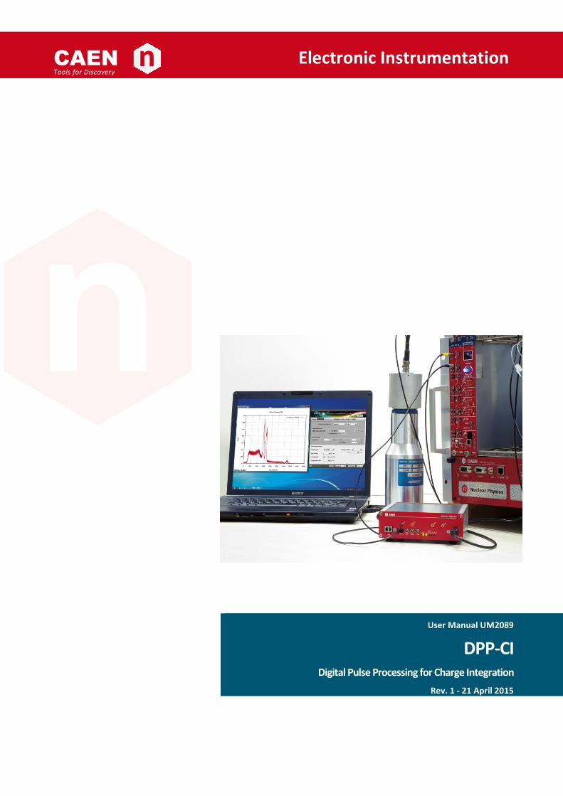
User Manual UM2089
DPP-CI Digital Pulse Processing for Charge Integration
Rev. 1 - 21 April 2015
Purpose of this Manual This User Manual contains the full description of the Digital Pulse Charge Integration for 720 Digitizer series. The description is only compliant with DPP-CI firmware release 4.5_130.23, and DPP-CI Control Software release 1.2.4. For future release compatibility check in the firmware and software revision history files.
Change Document Record Date Revision Changes
08 May 2013 00 Initial release
21 April 2015 01 Added support for firmware revision 4.5_130.23
Symbols, abbreviated terms and notation ADC Analog-to-Digital Converter DAQ Data Acquisition DPCI Digital Pulse Charge Integration DPP Digital Pulse Processing DPP-CI DPP for Charge Integration DPP-PSD DPP for Pulse Shape Discrimination MCA Multi-Channel Analyzer OS Operating System PC Personal Computer PMT Photo Multiplier Tube QDC Charge-to-Digital Converter TDC Time-to-Digital Converter USB Universal Serial Bus
Reference Documents [RD1] WP2081 - Digital Pulse Processing in Nuclear Physics
[RD2] UM2580 – DPSD User Manual
[RD3] AN2506 - Digital Gamma Neutron discrimination with Liquid Scintillators
[RD4] GD2827 - How to make coincidences with CAEN digitizers
[RD5] DPP-CI Firmware Registers COMING SOON
[RD6] UM1935 - CAENDigitizer User & Reference Manual
[RD7] GD2783 – First Installation Guide to Desktop Digitizers & MCA
[RD8] GD2512 - CAENUpgrader QuickStart Guide
[RD9] AN2086 - Synchronization of a multi-board acquisition system with CAEN digitizers
[RD10] UM2784 – CAENDigitizer LabView User & Reference Manual
[RD11] Technical Information Manual of V1718 and VX1718 VME – USB2.0 Bridge
[RD12] Technical Information Manual of A3818 PCI Express Optical Link Controller
[RD13] Technical Information Manual of A2818 PCI Optical Link Controller
[RD14] UM1935 - CAENComm User & Reference Manual
[RD15] AN2472 - CONET1 to CONET2 migration
All documents can be downloaded from: http://www.caen.it/csite/LibrarySearch.jsp
CAEN S.p.A. Via Vetraia, 11 55049 Viareggio (LU) - ITALY Tel. +39.0584.388.398 Fax +39.0584.388.959 [email protected] www.caen.it
© CAEN SpA – 2015
Disclaimer
No part of this manual may be reproduced in any form or by any means, electronic, mechanical, recording, or otherwise, without the prior written permission of CAEN SpA.
The information contained herein has been carefully checked and is believed to be accurate; however, no responsibility is assumed for inaccuracies. CAEN SpA reserves the right to modify its products specifications without giving any notice; for up to date information please visit www.caen.it.
MADE IN ITALY : We stress the fact that all the boards are made in Italy because in this globalized world, where getting the lowest possible price for products sometimes translates into poor pay and working conditions for the people who make them, at least you know that who made your board was reasonably paid and worked in a safe environment. (this obviously applies only to the boards marked "MADE IN ITALY", we cannot attest to the manufacturing process of "third party" boards).
CAEN Electronic Instrumentation
UM2089 – DPP-CI User Manual rev. 1 4
Index Purpose of this Manual ............................................................................................................................................. 2 Change Document Record ........................................................................................................................................ 2 Symbols, abbreviated terms and notation ............................................................................................................... 2 Reference Documents .............................................................................................................................................. 2
Index.......................................................................................................................................... 4
List of Figures ............................................................................................................................. 4
List of Tables .............................................................................................................................. 5
1 Introduction ....................................................................................................................... 6
2 Principle of Operation ........................................................................................................ 9 Baseline ................................................................................................................................................................... 11 DPP-CI trigger management ................................................................................................................................... 12
3 Acquisition modes ............................................................................................................ 13
4 Memory Organization ...................................................................................................... 14 720 series .............................................................................................................................................................................15
Event Data Format .................................................................................................................................................. 16 Channel Aggregate Data Format for 720 series ..................................................................................................................16 Board Aggregate Data Format ............................................................................................................................................18 Data Block ............................................................................................................................................................................19
5 Getting Started ................................................................................................................. 20 Aim of the chapter .................................................................................................................................................. 20 System Overview .................................................................................................................................................... 20 Hardware Setup ...................................................................................................................................................... 20 Drivers and Software .............................................................................................................................................. 21 Firmware and Licensing .......................................................................................................................................... 22 Practical Use ........................................................................................................................................................... 24
6 Coincidences and Synchronization .................................................................................... 52
7 Software Interface ............................................................................................................ 53 Introduction ............................................................................................................................................................ 53 Block Diagram ......................................................................................................................................................... 53 Drivers & Libraries .................................................................................................................................................. 54
Drivers ..................................................................................................................................................................................54 Libraries ...............................................................................................................................................................................54
Installation .............................................................................................................................................................. 56 GUI Description ....................................................................................................................................................... 57
The Tab “General” ...............................................................................................................................................................58 The Tab “Channels” .............................................................................................................................................................60 The Tab “Oscilloscope” ........................................................................................................................................................63 The Tab “Histogram” ...........................................................................................................................................................65 The Tab “Stats” ....................................................................................................................................................................67 The Tab “Output” ................................................................................................................................................................68 The Tab “Logger” .................................................................................................................................................................70
Config File Sintax ..................................................................................................................................................... 71 Notes on Firmware and Licensing ........................................................................................................................... 73
8 Technical support ............................................................................................................. 74
List of Figures Fig. 1.1: Simplified block diagram of the Digitizer ............................................................................................................................... 7 Fig. 2.1: functional block diagram of DPP-CI firmware ........................................................................................................................ 9 Fig. 2.2: Diagram summarizing the DPP-CI parameters. The trigger fires as soon as the signal crosses the threshold value. Gate, Gate Offset, Pre-Trigger, Trigger Hold-Off, and Record Length are also shown for one acquisition window ................................... 10 Fig. 2.3: Baseline calculation as managed by the DPP-CI algorithm .................................................................................................. 11 Fig. 2.4: Diagram showing the structure of the trigger management of the DPP-CI firmware .......................................................... 12 Fig. 3.1: Data organization into the Internal Memory of x720 digitizer ............................................................................................. 15 Fig. 3.2: Channel Aggregate Data Format scheme for 720 series ...................................................................................................... 16 Fig. 3.3: Board Aggregate Data Format scheme ................................................................................................................................ 18
CAEN Electronic Instrumentation
5 UM2089 – DPP-CI User Manual rev. 1
Fig. 3.4: Data Block scheme ............................................................................................................................................................... 19 Fig. 4.1: CAEN DPP-CI System components ....................................................................................................................................... 20 Fig. 4.2: Hardware and software setup for the DPP-CI practical application ..................................................................................... 20 Fig. 4.3: CAENUpgrader settings for DPP-CI firmware upgrade. ........................................................................................................ 23 Fig. 4.4: Input signal DC offset adjustment description. .................................................................................................................... 33 Fig. 6.1: The DPP-CI Control Software block diagram ........................................................................................................................ 53 Fig. 6.2: Libraries and drivers required for the DPP-CI system .......................................................................................................... 55 Fig. 6.3: Common Bar ........................................................................................................................................................................ 57 Fig. 6.4: Tab “General”....................................................................................................................................................................... 58 Fig. 6.5: Connection Window ............................................................................................................................................................. 59 Fig. 6.6: Tab “Channels” ..................................................................................................................................................................... 60 Fig. 6.7: Input signal DC offset adjustment description ..................................................................................................................... 61 Fig. 6.8: Tab “Oscilloscope” ............................................................................................................................................................... 63 Fig. 6.9: The Trace Settings Window.................................................................................................................................................. 64 Fig. 6.10: Tab “Histogram” ................................................................................................................................................................. 65 Fig. 6.11: Energy Calibration window ................................................................................................................................................ 66 Fig. 6.12: Tab “Stats” ......................................................................................................................................................................... 67 Fig. 6.13: Tab “Output” ...................................................................................................................................................................... 68 Fig. 6.14: Warning message about data saving ................................................................................................................................. 69 Fig. 6.15: Tab “Logger” ...................................................................................................................................................................... 70 Fig. 6.16: Firmware unlicensed warning message ............................................................................................................................. 73
List of Tables Tab. 4.2: Examples of connection settings ........................................................................................................................................ 25 Tab. 6.2: Table of the Connection icon values ................................................................................................................................... 57 Tab. 6.3: Examples of connection settings ........................................................................................................................................ 59
CAEN Electronic Instrumentation
UM2089 – DPP-CI User Manual rev. 1 6
1 Introduction CAEN S.p.A offers a wide range of digitizers for different needs of sampling frequency, resolution, form factor, etc. Besides the use of the digitizers as a waveform recorder only (oscilloscope mode), the user can upload special versions of the FPGA firmware for the Digital Pulse Processing (DPP) algorithms. A digitizer running in DPP mode becomes a multipurpose instrument which replaces most of the traditional modules such as MCAs, QDCs, TDCs, Discriminators, etc. (for more details refer to the DPP overview [RD1]). CAEN provides two algorithms for the charge integration of the digitized input pulses at the firmware level:
the Digital Pulse Processing for Charge Integration firmware (DPP-CI), single gate compatible to the 720 series digitizers (featuring both the EP1C4 and the EP1C20 Altera FPGA models).
the Digital Pulse Processing for Pulse Shape Discrimination firmware (DPP-PSD), dual gate, running only on the 720 series digitizers (12 bit, 250MS/s) with the EP1C20 FPGA, and on the 751 series digitizers (10 bit, 1 GS/s; DES mode not supported). The DPP-PSD firmware allows for charge integration in two different gate widths to discriminate short and long components of the signal. For more details and examples, as the gamma-neutron discrimination, see [RD2] and [RD3].
This manual describes in details the DPP-CI algorithm, suitable for those models summarized in Table 1. The use of DPP-CI is particularly recommended for digitizers with EP1C4 FPGA, where the DPP-PSD is not supported for limitations on the FPGA memory. All the DPP-CI functionalities are included in the DPP-PSD firmware.
Note: The description of the DPP-CI system of this Manual is only compliant with DPP-CI firmware release 4.5_130.23, and DPP-CI Control Software release 1.2.4. For future release compatibility check in the firmware and software revision history files.
Desktop Digitizers(*)
Description Product Code
DT5720 4 Ch. 12 bit 250 MS/s Digitizer: 1.25MS/ch, C4, SE WDT5720XAAAA
DT5720A 2 Ch. 12 bit 250 MS/s Digitizer: 1.25MS/ch, C4, SE WDT5720AXAAA DT5720B 4 Ch. 12 bit 250 MS/s Digitizer: 1.25MS/ch, C20, SE WDT5720BXAAA
DT5720C 2 Ch. 12 bit 250 MS/s Digitizer: 1.25MS/ch, C20, SE WDT5720CXAAA
DT5720D 4 Ch. 12 bit 250 MS/s Digitizer: 10MS/ch, C20, SE WDT5720DXAAA DT5720E 2 Ch. 12 bit 250 MS/s Digitizer: 10MS/ch, C20, SE WDT5720EXAAA
NIM Digitizers(*) Description Product Code
N6720 4 Ch. 12 bit 250 MS/s Digitizer: 1.25MS/ch, C4, SE WN6720XAAAAA N6720A 2 Ch. 12 bit 250 MS/s Digitizer: 1.25MS/ch, C4, SE WN6720AXAAAA
N6720B 4 Ch. 12 bit 250 MS/s Digitizer: 1.25MS/ch, C20, SE WN6720BXAAAA
N6720C 2 Ch. 12 bit 250 MS/s Digitizer: 1.25MS/ch, C20, SE WN6720CXAAAA N6720D 4 Ch. 12 bit 250 MS/s Digitizer: 10MS/ch, C20, SE WN6720DXAAAA
N6720E 2 Ch. 12 bit 250 MS/s Digitizer: 10MS/ch, C20, SE WN6720EXAAAA VME Digitizers(*) Description Product Code
V1720 8 Ch. 12 bit 250 MS/s Digitizer: 1.25MS/ch, C4, SE WV1720XAAAAA
V1720B 8 Ch. 12 bit 250 MS/s Digitizer: 10MS/ch, C4, SE WV1720BXAAAA V1720C 8 Ch. 12 bit 250 MS/s Digitizer: 1.25MS/ch, C4, DIFF WV1720CXAAAA
V1720D 8 Ch. 12 bit 250 MS/s Digitizer: 10MS/ch, C4, DIFF WV1720DXAAAA
V1720E 8 Ch. 12 bit 250 MS/s Digitizer: 1.25MS/ch, C20, SE WV1720EXAAAA V1720F 8 Ch. 12 bit 250 MS/s Digitizer: 1.25MS/ch, C20, DIFF WV1720FXAAAA
V1720G 8 Ch. 12 bit 250 MS/s Digitizer: 10MS/ch, C20, SE WV1720GXAAAA
DPP Firmware(*) Description Product Code DPP-CI Digital Pulse Processing for Charge Integration for (x720) WFWDPPCIAAAA
Table 1: Supported CAEN digitizers for DPP-CI firmware
(*) For accessories and customizations related to digitizers and for multiple DPP-CI license packs, refer to the specific board User Manual or check in the CAEN web site: www.caen.it
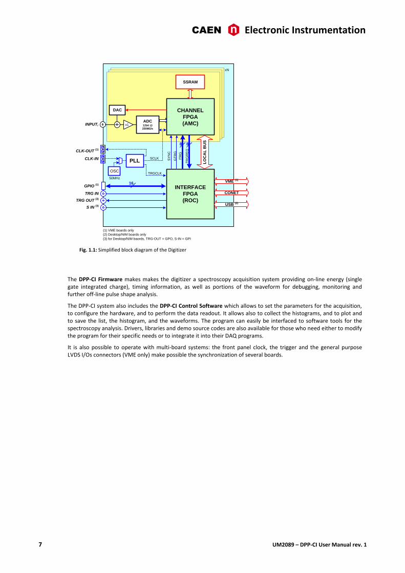
The analog input signal is continuously converted into a stream of digital samples and on-line processed by the Channel FPGA (AMC). The AMC purpose is to perform the on-line Digital Pulse Processing to implement a Charge Integration MCA (DPP-CI). A simplified block diagram of the module is shown in Fig. 1.1.
CAEN Electronic Instrumentation
7 UM2089 – DPP-CI User Manual rev. 1
TRG OUT (3)
CLK-OUT (1)
CLK-IN
TRG IN
S IN (3)
LO
CA
L B
US
SSRAM
VME (1)
PLL
CONET
INPUTi
SY
NC
GT
RG
ITR
G
TR
GR
EQ
GPIO (1) 16
8 8
ADC12bit @
250MS/s
DAC CHANNEL
FPGA
(AMC)
INTERFACE
FPGA
(ROC)USB
(2)
OSC
(1) VME boards only
(2) Desktop/NIM boards only
(3) for Desktop/NIM baords, TRG-OUT = GPO, S-IN = GPI
50MHz
x1
SCLK
TRGCLK
xN
Fig. 1.1: Simplified block diagram of the Digitizer
The DPP-CI Firmware makes makes the digitizer a spectroscopy acquisition system providing on-line energy (single gate integrated charge), timing information, as well as portions of the waveform for debugging, monitoring and further off-line pulse shape analysis.
The DPP-CI system also includes the DPP-CI Control Software which allows to set the parameters for the acquisition, to configure the hardware, and to perform the data readout. It allows also to collect the histograms, and to plot and to save the list, the histogram, and the waveforms. The program can easily be interfaced to software tools for the spectroscopy analysis. Drivers, libraries and demo source codes are also available for those who need either to modify the program for their specific needs or to integrate it into their DAQ programs.
It is also possible to operate with multi-board systems: the front panel clock, the trigger and the general purpose LVDS I/Os connectors (VME only) make possible the synchronization of several boards.
CAEN Electronic Instrumentation
UM2089 – DPP-CI User Manual rev. 1 8
The following list summarizes what the user can do with the DPP-CI system:
receive an input signal and digitize it continuously at 250MS/s;
adjust the dynamic range (programmable DC offset);
calculate the baseline and subtract it from the input signal (Digital Baseline Restorer);
detect input pulses and generate a local trigger on them (refer to Sect. DPP-CI trigger management for
further details);
calculate the time of arrival of the trigger;
integrate the charge (Q) inside the integration gate window;
build the event through a configurable combination of Trigger Time Stamp, Q, baseline and raw waveforms
(i.e. series of ADC samples belonging to a programmable size acquisition window);
implement coincidences between channels of the same board ([RD4]) as well as among channels of
different boards through the LVDS I/O connectors (VME only), external trigger, and external modules;
save events (list) into a memory buffer and manage the readout through Optical Link, USB or VME;
plot the signal waveforms (oscilloscope mode) and make online adjustments of the acquisition parameters;
plot energy spectrum of Q and timing distribution;
generate output files (list and waveform) in different formats suitable for external spectroscopy analysis
software tools. Energy and time histograms are not managed onboard but they can be generated and
saved by the DPP-CI Control Software.
CAEN Electronic Instrumentation
9 UM2089 – DPP-CI User Manual rev. 1
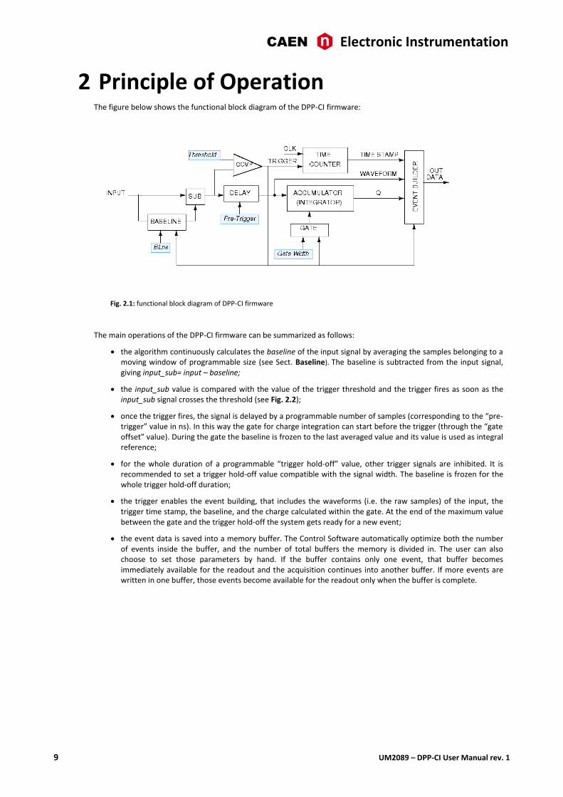
2 Principle of Operation The figure below shows the functional block diagram of the DPP-CI firmware:
Fig. 2.1: functional block diagram of DPP-CI firmware
The main operations of the DPP-CI firmware can be summarized as follows:
the algorithm continuously calculates the baseline of the input signal by averaging the samples belonging to a moving window of programmable size (see Sect. Baseline). The baseline is subtracted from the input signal, giving input_sub= input – baseline;
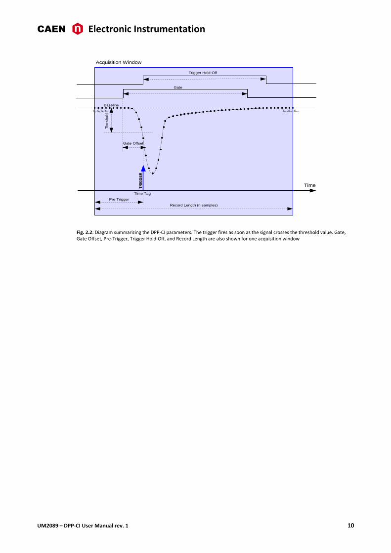
the input_sub value is compared with the value of the trigger threshold and the trigger fires as soon as the input_sub signal crosses the threshold (see Fig. 2.2);
once the trigger fires, the signal is delayed by a programmable number of samples (corresponding to the “pre-trigger” value in ns). In this way the gate for charge integration can start before the trigger (through the “gate offset” value). During the gate the baseline is frozen to the last averaged value and its value is used as integral reference;
for the whole duration of a programmable “trigger hold-off” value, other trigger signals are inhibited. It is recommended to set a trigger hold-off value compatible with the signal width. The baseline is frozen for the whole trigger hold-off duration;
the trigger enables the event building, that includes the waveforms (i.e. the raw samples) of the input, the trigger time stamp, the baseline, and the charge calculated within the gate. At the end of the maximum value between the gate and the trigger hold-off the system gets ready for a new event;
the event data is saved into a memory buffer. The Control Software automatically optimize both the number of events inside the buffer, and the number of total buffers the memory is divided in. The user can also choose to set those parameters by hand. If the buffer contains only one event, that buffer becomes immediately available for the readout and the acquisition continues into another buffer. If more events are written in one buffer, those events become available for the readout only when the buffer is complete.
CAEN Electronic Instrumentation
UM2089 – DPP-CI User Manual rev. 1 10
Gate Offset
Baseline
Acquisition Window
Time
S0 S1 S2 S3 Sn-1Sn-2Sn-3
Gate
Th
resh
old
TR
IGG
ER
Pre Trigger
Record Length (n samples)
Time Tag
Trigger Hold-Off
Fig. 2.2: Diagram summarizing the DPP-CI parameters. The trigger fires as soon as the signal crosses the threshold value. Gate, Gate Offset, Pre-Trigger, Trigger Hold-Off, and Record Length are also shown for one acquisition window
CAEN Electronic Instrumentation
11 UM2089 – DPP-CI User Manual rev. 1
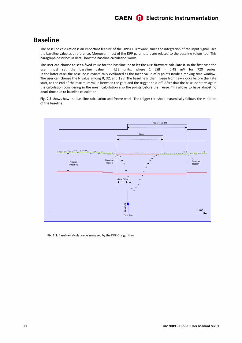
Baseline The baseline calculation is an important feature of the DPP-CI Firmware, since the integration of the input signal uses the baseline value as a reference. Moreover, most of the DPP parameters are related to the baseline values too. This paragraph describes in detail how the baseline calculation works.
The user can choose to set a fixed value for the baseline, or to let the DPP firmware calculate it. In the first case the user must set the baseline value in LSB units, where 1 LSB = 0.48 mV for 720 series. In the latter case, the baseline is dynamically evaluated as the mean value of N points inside a moving time window. The user can choose the N value among 8, 32, and 128. The baseline is then frozen from few clocks before the gate start, to the end of the maximum value between the gate and the trigger hold-off. After that the baseline starts again the calculation considering in the mean calculation also the points before the freeze. This allows to have almost no dead-time due to baseline calculation.
Fig. 2.3 shows how the baseline calculation and freeze work. The trigger threshold dynamically follows the variation of the baseline.
Gate
Time
Trigger
Threshold
TR
IGG
ER
Gate Offset
Time Tag
Trigger Hold-Off
Baseline
FreezeBaseline
Restart
Fig. 2.3: Baseline calculation as managed by the DPP-CI algorithm
CAEN Electronic Instrumentation
UM2089 – DPP-CI User Manual rev. 1 12
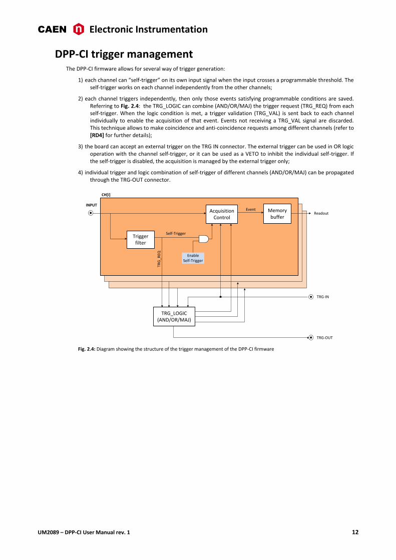
DPP-CI trigger management The DPP-CI firmware allows for several way of trigger generation:
1) each channel can “self-trigger” on its own input signal when the input crosses a programmable threshold. The self-trigger works on each channel independently from the other channels;
2) each channel triggers independently, then only those events satisfying programmable conditions are saved. Referring to Fig. 2.4: the TRG_LOGIC can combine (AND/OR/MAJ) the trigger request (TRG_REQ) from each self-trigger. When the logic condition is met, a trigger validation (TRG_VAL) is sent back to each channel individually to enable the acquisition of that event. Events not receiving a TRG_VAL signal are discarded. This technique allows to make coincidence and anti-coincidence requests among different channels (refer to [RD4] for further details);
3) the board can accept an external trigger on the TRG IN connector. The external trigger can be used in OR logic operation with the channel self-trigger, or it can be used as a VETO to inhibit the individual self-trigger. If the self-trigger is disabled, the acquisition is managed by the external trigger only;
4) individual trigger and logic combination of self-trigger of different channels (AND/OR/MAJ) can be propagated through the TRG-OUT connector.
Trigger filter
Acquisition Control
Memory buffer
TRG_LOGIC(AND/OR/MAJ)
Enable Self-Trigger
Event
Self-Trigger
TRG
_REQ
Readout
INPUT
TRG-IN
TRG-OUT
CH[i]
Fig. 2.4: Diagram showing the structure of the trigger management of the DPP-CI firmware
CAEN Electronic Instrumentation
13 UM2089 – DPP-CI User Manual rev. 1
3 Acquisition modes
As described on Sect. DPP-CI trigger management each individual channel of the digitizer can trigger independently from the others. When the input signal fires the trigger the DPP-CI firmware integrates the input samples within the programmed time window.
The main acquisition mode is called “List mode”, where the digitizer provides the time of arrival of the input (also called “Trigger Time Stamp”) and its charge. As soon as the list reaches a certain size, it is made available for readout and the acquisition continues in another buffer. Being the size of the event very small (typically few bytes), the throughput is extremely reduced. The firmware is not designed to make histogram onboard, anyway it can transfer the list information to the software for the histogram management.
The DPP-CI firmware allows also to acquire waveform samples (i.e. a sequence of samples within a programmable acquisition window) in the “Waveform” acquisition mode. This acquisition mode is mainly intended to debug and to set the DPP parameters. For each trigger (internal or external), the digitizer saves a portion of the waveform into a local memory buffer. Running in Oscilloscope Mode, the user can view the input signal, the baseline, and other control signals (such as the trigger, the gate, the trigger hold-off, etc…) in the same plot, and easily adjust the parameters for the acquisition. Running in oscilloscope mode implies a very high data throughput, due to the huge amount of samples saved into the board memory and then read out by the DAQ software.
The DPP-CI firmware can manage both acquisition modes together in the “Mixed” acquisition mode, where it is possible to read the charge, the baseline and the time stamp information together with a portion of the waveform, so that the user can retrieve further information and use it off-line, still keeping a reasonable level of throughput bandwidth
The DPP-CI Control Software can manage both the list and the waveform acquisition mode, with the exception of the mixed mode. In the list mode the software can retrieve the list information from the digitizer to make the relevant histogram and save the output files. Working in waveform mode the software can plot the digital pulse for online monitoring and save the output file. Users who wants to acquire in mixed mode have to write their own software. Example codes are available in the Samples folder of the CAENDigitizer library package [RD6].
CAEN Electronic Instrumentation
UM2089 – DPP-CI User Manual rev. 1 14
4 Memory Organization Each channel has a fixed amount of RAM memory to save the events. The memory is divided into a programmable number of buffers (also called “aggregates”), where each buffer contains a programmable number of events. The event format is programmable as well. The board registers involved are the following:
• BUFF_ORG (Nb): defines the total number of buffers (i.e. aggregates) in which the memory is divided
( Nbbuffersnum 2.. ).
• NEV_AGGREGATE (Ne): defines the number of events contained in one aggregate. The maximum allowed value is 1023.
• RECORD_LENGTH (Ns): defines the number of samples of the waveform, if enabled (Ns = 8 * CUST.SIZE for 720 series, where CUST.SIZE is the value written in the register).
• CONFIG: defines the acquisition mode and the event data format.
For a detailed description, refer to the specific User Manual and [RD5]. Information about the use of these parameters in the CAENDigitizer library can be found in [RD6].
According to the programmed event format, an event can contain a certain number of samples of the waveform, one trigger time stamp, the charge Q and the baseline.
Note: Those who need to write their own DAQ software, must take care to choose the Ne value accordingly to the event and buffer size, as explained in the examples in the next section.
CAEN Electronic Instrumentation
15 UM2089 – DPP-CI User Manual rev. 1
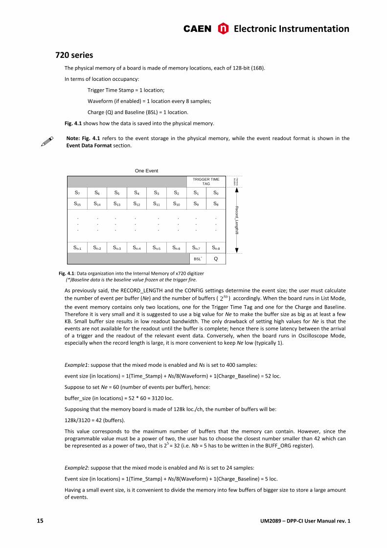
720 series
The physical memory of a board is made of memory locations, each of 128-bit (16B).
In terms of location occupancy:
Trigger Time Stamp = 1 location;
Waveform (if enabled) = 1 location every 8 samples;
Charge (Q) and Baseline (BSL) = 1 location.
Fig. 4.1 shows how the data is saved into the physical memory.
Note: Fig. 4.1 refers to the event storage in the physical memory, while the event readout format is shown in the Event Data Format section.
As previously said, the RECORD_LENGTH and the CONFIG settings determine the event size; the user must calculate
the number of event per buffer (Ne) and the number of buffers ( Nb2 ) accordingly. When the board runs in List Mode,
the event memory contains only two locations, one for the Trigger Time Tag and one for the Charge and Baseline. Therefore it is very small and it is suggested to use a big value for Ne to make the buffer size as big as at least a few KB. Small buffer size results in low readout bandwidth. The only drawback of setting high values for Ne is that the events are not available for the readout until the buffer is complete; hence there is some latency between the arrival of a trigger and the readout of the relevant event data. Conversely, when the board runs in Oscilloscope Mode, especially when the record length is large, it is more convenient to keep Ne low (typically 1).
Example1: suppose that the mixed mode is enabled and Ns is set to 400 samples:
event size (in locations) = 1(Time_Stamp) + Ns/8(Waveform) + 1(Charge_Baseline) = 52 loc.
Suppose to set Ne = 60 (number of events per buffer), hence:
buffer_size (in locations) = 52 * 60 = 3120 loc.
Supposing that the memory board is made of 128k loc./ch, the number of buffers will be:
128k/3120 = 42 (buffers).
This value corresponds to the maximum number of buffers that the memory can contain. However, since the programmable value must be a power of two, the user has to choose the closest number smaller than 42 which can be represented as a power of two, that is 2
5 = 32 (i.e. Nb = 5 has to be written in the BUFF_ORG register).
Example2: suppose that the mixed mode is enabled and Ns is set to 24 samples:
Event size (in locations) = 1(Time_Stamp) + Ns/8(Waveform) + 1(Charge_Baseline) = 5 loc.
Having a small event size, is it convenient to divide the memory into few buffers of bigger size to store a large amount of events.
S0
S8
S7
Sn-8
S15
Sn-1
TRIGGER TIME
TAG
S11
S3
Sn-5
One Event
Re
co
rd_
Le
ng
th/8
Sn-7Sn-6
S1S2
S9S10
S4S5S6
S13 S12S14
Sn-3Sn-2 Sn-4
.
.
.
.
.
.
.
.
.
.
.
.
.
.
.
.
.
.
.
.
.
.
.
.
BSL* Q
me
mo
ry
loca
tion
Fig. 4.1: Data organization into the Internal Memory of x720 digitizer (*)Baseline data is the baseline value frozen at the trigger fire.
CAEN Electronic Instrumentation
UM2089 – DPP-CI User Manual rev. 1 16
Suppose to have set Nb = 3, so that the number of buffers is 8.
Supposing that the board memory option is made of 64k locations, each buffer consists in 64k/8 = 8k locations and so the resulting number of event per aggregate should be:
Ne = 8k/5 = 1639.
IMPORTANT: in this case, the real number of events stored per aggregate is 1023, due to the register length constraint already mentioned.
Event Data Format When the data readout is performed, the data format will appear as follows.
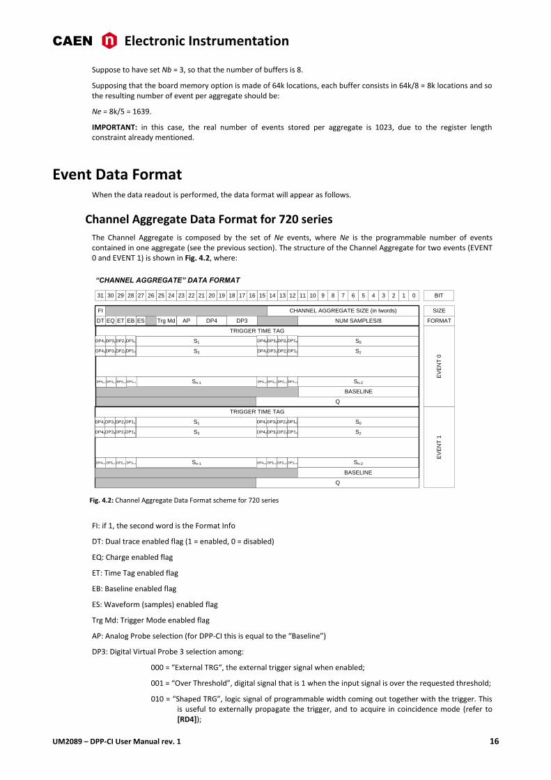
Channel Aggregate Data Format for 720 series
The Channel Aggregate is composed by the set of Ne events, where Ne is the programmable number of events contained in one aggregate (see the previous section). The structure of the Channel Aggregate for two events (EVENT 0 and EVENT 1) is shown in Fig. 4.2, where:
FI: if 1, the second word is the Format Info
DT: Dual trace enabled flag (1 = enabled, 0 = disabled)
EQ: Charge enabled flag
ET: Time Tag enabled flag
EB: Baseline enabled flag
ES: Waveform (samples) enabled flag
Trg Md: Trigger Mode enabled flag
AP: Analog Probe selection (for DPP-CI this is equal to the “Baseline”)
DP3: Digital Virtual Probe 3 selection among:
000 = “External TRG“, the external trigger signal when enabled;
001 = “Over Threshold”, digital signal that is 1 when the input signal is over the requested threshold;
010 = “Shaped TRG”, logic signal of programmable width coming out together with the trigger. This is useful to externally propagate the trigger, and to acquire in coincidence mode (refer to [RD4]);
PUR
ES DP4
FI
“CHANNEL AGGREGATE” DATA FORMAT
012345631 789101112131415161718192021222324252627282930
CHANNEL AGGREGATE SIZE (in lwords)
BASELINE
D0'
D0 S0S1
DT NUM SAMPLES/8
TRIGGER TIME TAG
EQ ET EB AP DP3
S2S3
Sn-2Sn-1
TRIGGER TIME TAG
EV
EN
T 0
SIZE
FORMAT
EV
EN
T 1
Q
DP00
D2'
D2 Gl2 Gs2
D1'
D1 Gl1 Gs1
D3'
D3 Gl3 Gs3
Dn2'
Dn2 Gln2Gsn2Dn1' Dn1 Gln1 Gsn1
D0 S0S1
S2S3
Sn-2Sn-1
QSHORTQLONG
Gl0 Gs0
D2'
D2 Gl2 Gs2
D1'
D1 Gl1 Gs1
D3'
D3 Gl3 Gs3
Dn2'
Dn2 Gln2Gsn2Dn1'
Dn1 Gln1 Gsn1
Trg Md
D0'
DP20DP30DP40 DP10
DP22DP32DP42 DP12
DP21DP41DP31 DP11
DP23DP33DP43 DP13
DP2n-1DP3n-1DP4n-1 DP1n-1 DP2n-2DP3n-2DP4n-2 DP1n-2
DP20DP30DP40 DP10
DP22DP32DP42 DP12
DP21DP31DP41 DP11
DP23DP33DP43 DP13
DP2n-1DP3n-1DP4n-1 DP1n-1 DP2n-2DP3n-2DP4n-2 DP1n-2
BASELINE
Q
BIT
Fig. 4.2: Channel Aggregate Data Format scheme for 720 series
CAEN Electronic Instrumentation
17 UM2089 – DPP-CI User Manual rev. 1
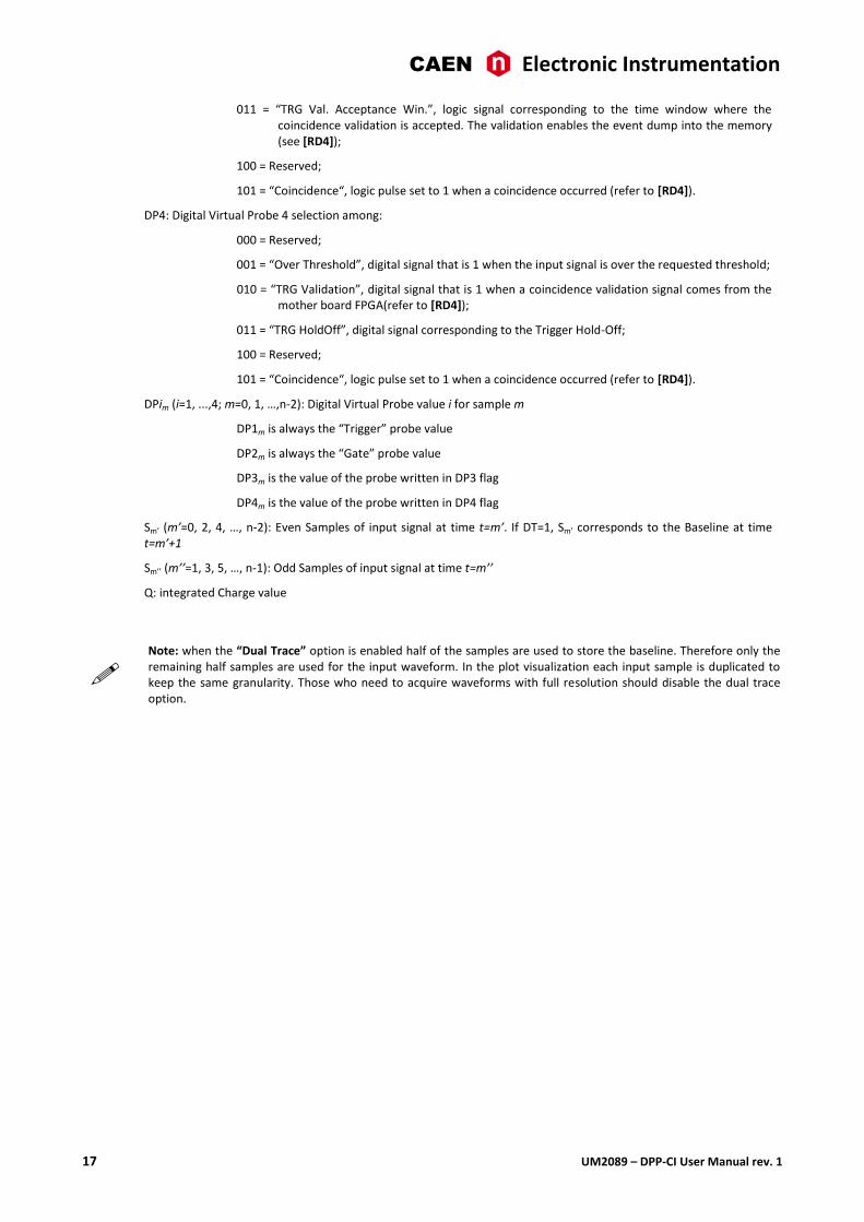
011 = “TRG Val. Acceptance Win.”, logic signal corresponding to the time window where the coincidence validation is accepted. The validation enables the event dump into the memory (see [RD4]);
100 = Reserved;
101 = “Coincidence“, logic pulse set to 1 when a coincidence occurred (refer to [RD4]).
DP4: Digital Virtual Probe 4 selection among:
000 = Reserved;
001 = “Over Threshold”, digital signal that is 1 when the input signal is over the requested threshold;
010 = “TRG Validation”, digital signal that is 1 when a coincidence validation signal comes from the mother board FPGA(refer to [RD4]);
011 = “TRG HoldOff”, digital signal corresponding to the Trigger Hold-Off;
100 = Reserved;
101 = “Coincidence“, logic pulse set to 1 when a coincidence occurred (refer to [RD4]).
DPim (i=1, ...,4; m=0, 1, …,n-2): Digital Virtual Probe value i for sample m
DP1m is always the “Trigger” probe value
DP2m is always the “Gate” probe value
DP3m is the value of the probe written in DP3 flag
DP4m is the value of the probe written in DP4 flag
Sm’ (m’=0, 2, 4, …, n-2): Even Samples of input signal at time t=m’. If DT=1, Sm’ corresponds to the Baseline at time t=m’+1
Sm’’ (m’’=1, 3, 5, …, n-1): Odd Samples of input signal at time t=m’’
Q: integrated Charge value
Note: when the “Dual Trace” option is enabled half of the samples are used to store the baseline. Therefore only the remaining half samples are used for the input waveform. In the plot visualization each input sample is duplicated to keep the same granularity. Those who need to acquire waveforms with full resolution should disable the dual trace option.
CAEN Electronic Instrumentation
UM2089 – DPP-CI User Manual rev. 1 18
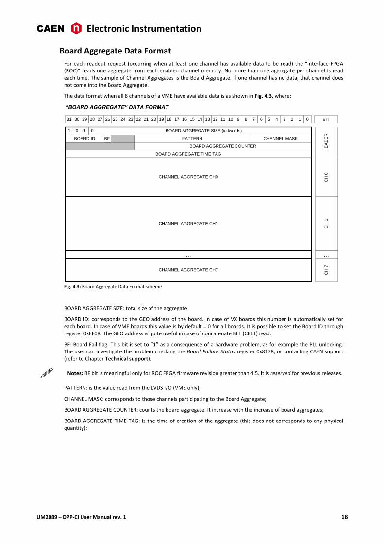
Board Aggregate Data Format
For each readout request (occurring when at least one channel has available data to be read) the “interface FPGA (ROC)” reads one aggregate from each enabled channel memory. No more than one aggregate per channel is read each time. The sample of Channel Aggregates is the Board Aggregate. If one channel has no data, that channel does not come into the Board Aggregate.
The data format when all 8 channels of a VME have available data is as shown in Fig. 4.3, where:
012345631 789101112131415161718192021222324252627282930
01 BOARD AGGREGATE SIZE (in lwords)01
CHANNEL MASKPATTERNBOARD ID
BOARD AGGREGATE COUNTER
BOARD AGGREGATE TIME TAG
HE
AD
ER
CHANNEL AGGREGATE CH0
CH
0C
H 1
CHANNEL AGGREGATE CH7
CH
7
CHANNEL AGGREGATE CH1
“BOARD AGGREGATE” DATA FORMAT
... ...
BIT
BF
Fig. 4.3: Board Aggregate Data Format scheme
BOARD AGGREGATE SIZE: total size of the aggregate
BOARD ID: corresponds to the GEO address of the board. In case of VX boards this number is automatically set for each board. In case of VME boards this value is by default = 0 for all boards. It is possible to set the Board ID through register 0xEF08. The GEO address is quite useful in case of concatenate BLT (CBLT) read.
BF: Board Fail flag. This bit is set to “1” as a consequence of a hardware problem, as for example the PLL unlocking. The user can investigate the problem checking the Board Failure Status register 0x8178, or contacting CAEN support (refer to Chapter Technical support).
Notes: BF bit is meaningful only for ROC FPGA firmware revision greater than 4.5. It is reserved for previous releases.
PATTERN: is the value read from the LVDS I/O (VME only);
CHANNEL MASK: corresponds to those channels participating to the Board Aggregate;
BOARD AGGREGATE COUNTER: counts the board aggregate. It increase with the increase of board aggregates;
BOARD AGGREGATE TIME TAG: is the time of creation of the aggregate (this does not corresponds to any physical quantity);

CAEN Electronic Instrumentation
19 UM2089 – DPP-CI User Manual rev. 1
Data Block
The readout of the digitizer is done using the Block Transfer (BLT, refer to [RD6]); for each transfer, the board gives a certain number of Board Aggregates, consisting in the Data Block. The maximum number of aggregates that can be transferred in a BLT is defined by the READOUT_BTL_AGGREGATE_NUMBER. In the final readout each Board Aggregate comes successively. In case of n Board Aggregates, the Data Block is as in Fig. 4.4.
BOARD AGGREGATE n-1
DATA BLOCK
BOARD AGGREGATE 1
BOARD AGGREGATE 0
...
Fig. 4.4: Data Block scheme
CAEN Electronic Instrumentation
UM2089 – DPP-CI User Manual rev. 1 20
5 Getting Started Aim of the chapter
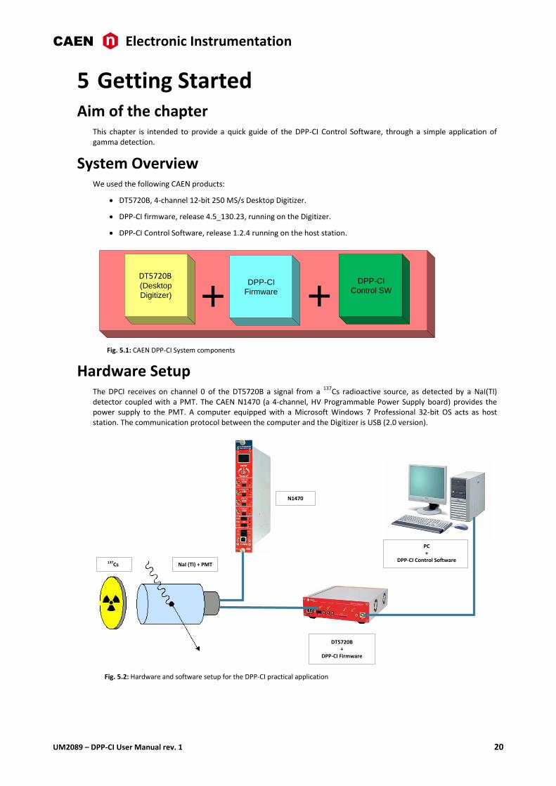
This chapter is intended to provide a quick guide of the DPP-CI Control Software, through a simple application of gamma detection.
System Overview We used the following CAEN products:
DT5720B, 4-channel 12-bit 250 MS/s Desktop Digitizer.
DPP-CI firmware, release 4.5_130.23, running on the Digitizer.
DPP-CI Control Software, release 1.2.4 running on the host station.
(Desktop
Digitizer)
DPP-CI
Firmware+ +DPP-CI
Control SW
DT5720B
Fig. 5.1: CAEN DPP-CI System components
Hardware Setup The DPCI receives on channel 0 of the DT5720B a signal from a
137Cs radioactive source, as detected by a NaI(Tl)
detector coupled with a PMT. The CAEN N1470 (a 4-channel, HV Programmable Power Supply board) provides the power supply to the PMT. A computer equipped with a Microsoft Windows 7 Professional 32-bit OS acts as host station. The communication protocol between the computer and the Digitizer is USB (2.0 version).
N1470
NaI (Tl) + PMT137Cs
DT5720B+
DPP-CI Firmware
PC +
DPP-CI Control Software
Fig. 5.2: Hardware and software setup for the DPP-CI practical application
CAEN Electronic Instrumentation
21 UM2089 – DPP-CI User Manual rev. 1
Drivers and Software In order to manage the DPP-CI System, the host station needs either Windows or Linux OS, and the third-party software Java Runtime Environment 7 or later (trademark of Oracle Inc., downloadable from http://www.java.com). Linux users must also take care of proper installation of gnuplot graphical tool, as well as of CAEN Libraries. The latter can be downloaded from CAEN website (login required before to download).
According to the preferred way of connection to the digitizer, users must also take care of proper installation of USB or optical drivers. In our case we are going to describe the procedure for USB connection.
DRIVERS
o USB 2.0 CAEN driver.
Note: If you’re using a different communication interface (i.e. Optical Link or VME), the related driver is required.
Note: It is recommended to install the driver before to connect the hardware.
Note: Detailed installation steps of CAEN USB drivers for communicating with desktop digitizers are described for several Microsoft Windows OSs in [RD7].
How to install the driver (Windows)
Download the latest release of the USB driver for Windows on CAEN website in the ‘Software/Firmware’ area at the DT5720 page.
Unpack the driver package.
Power on the Digitizer and plug the USB cable in a USB port on your computer.
Windows will try to find drivers and, in case of failure (the message “Device driver software was not successfully installed” may be displayed), the driver needs to be installed manually:
Go to the system’s Device Manager through the Control Panel and check for the CAEN DT5xxx USB1.0 unknown device.
Right click and select Driver software update in the scrolling menu.
Select the option to browse my computer for driver software.
Point to the driver folder and finalize the installation.
How to install the driver (Linux)
Download the latest release of the USB driver for Linux on CAEN website in the ‘Software/Firmware’ area at the DT5720 page.
Unpack the driver package (tar –zxf CAENUSBDrvB-xxx.tgz).
Go to the driver folder (cd CAENUSBDrvB-xxx).
Follow the instructions on the Readme.txt file.
Type: make
sudo make install
Reboot your machine
SOFTWARE
o DPP-CI Control Software for Windows OS.
Download the standalone DPP-CI Control Software full installation package on CAEN website in the ‘Download’ area at the DPP-CI Control Software page (login is required before the download).
Unpack the installation package, launch the setup file and complete the Installation wizard.
o DPP-CI Control Software for Linux.
Download the DPP-CI_ControlSoftware-xxx.tar.gz package on CAEN website in the ‘Download’ area at the DPP-CI Control Software page (login is required before the download).
Unpack the installation package (tar –zxf DPP-CI_ControlSoftware-xxx.tar.gz).
CAEN Electronic Instrumentation
UM2089 – DPP-CI User Manual rev. 1 22
Follow the instruction on Setup/Linux/Readme.txt
Type: ./configure
make
sudo make install
Launch the Control Software typing DPP-CI_ControlSoftware
Firmware and Licensing The DPP-CI Control Software controls digitizers running the DPP-CI Firmware.
How to install the firmware
Download the DPP-CI Firmware (.cfa) for 720 series on CAEN website in the ‘Download’ area at the DPP-CI page.
Download the CAENUpgrader software to upload the firmware on your board. The program full installation package for Windows OS is available on CAEN website in the ‘Download’ area at the CAENUpgrader page.
Unpack the installation package, launch the setup file and complete the Installation wizard.
Run the CAENUpgrader GUI by one of the following options:
The desktop icon for the program
The Quick Launch icon for the program
The .jar file in the bin folder from the installation path on your host
Select ‘Upgrade Firmware’ in the ‘Available actions’ scroll box menu of the ‘Board Upgrade’ tab.
Select the model of your board in the ‘Board Model’ scroll box menu.
Enter the .cfa file in the ‘Firmware binary file’ text box by the ‘Browse’ button.
Set ‘USB’ in the ‘Connection Type’ scroll box menu.
Set ‘0’ as ‘Link number’ setting.
Check ‘Standard Page’ in the ‘Config Options’.
Press the ‘Upgrade’ button to perform the upload; after few seconds, a pop up message will inform you about the successful upgrade.
Power cycle the board.
Note: in the Linux environment it is required to first install CAENVME, CAENComm and CAENDigitizer. You can find those libraries in the CAEN web page. In the Windows environment all libraries come within the control software package.
CAEN Electronic Instrumentation
23 UM2089 – DPP-CI User Manual rev. 1
Fig. 5.3: CAENUpgrader settings for DPP-CI firmware upgrade.
Note that when running the DPP-CI Control Software, the program checks for the firmware loaded in the target Digitizer. If no license is found, a pop-up warning message shows up and reports the time left before the acquisition is stopped (trial version). In order to unlock the DPP firmware and use it without any time limitation, you need to purchase a license from CAEN. Refer to [RD8] for detailed instructions on how to use CAENUpgrader and the licensing procedure.
CAEN Electronic Instrumentation
UM2089 – DPP-CI User Manual rev. 1 24
Practical Use The following step-by-step procedure shows how to use the DPP-CI Control Software (see Chapter 7) in an application of gamma ray detection, how to set the relevant DPP parameters and plot the signals (Oscilloscope mode), how to display the energy histogram (Histogram mode), and how to save the acquired data.
Check that the whole hardware in your setup is properly connected and powered on.
Note: After typing the value of a parameter in a box menu, press the “Enter” key on your keyboard to activate the setting.
1. Run the software.
After the DPP-CI Control Software installation, run the DPP-CI Control Software GUI, according to the options selected in the installation wizard, choosing one of the following options:
The Desktop icon for the program
The Quick Launch icon for the program
The .bat file in the main folder from the installation path on your host
CAEN Electronic Instrumentation
25 UM2089 – DPP-CI User Manual rev. 1
2. Connect to the Digitizer.
Path1: Tab GENERAL Section RUNNER
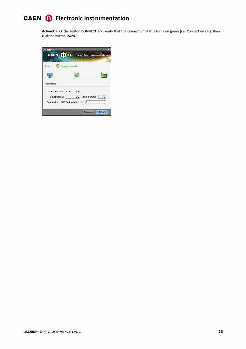
Action1: click the button CONNECT. The “Connection” window will appear.
Action2: set the connection parameters values. Using a USB communication link with a Desktop digitizer, the correct settings are: TYPE = “USB”, LINK = “0” and ADDRESS = “0”. Tab. 5.1 shows the setting values for common communication channels and Digitizers. Further examples are in Tab. 7.2.
Connection chain Type Link Slave Address
PC –> USB –> DT5720 / N6720 USB 0 0 0
PC –> USB –> V1718 –> VME –> V1720 USB 0 0 32100000*
PC –> PCI/PCIe –> A2818/A3818 –> CONET –> DT5720 / N6720 PCI 0 0 0
PC –> PCI/PCIe –> A2818/A3818 –> CONET –> V1720 PCI 0 0 32100000* Tab. 5.1: Examples of connection settings
(*)For the correct VME base address to be used, please refer to the Digitizer’s User Manual.
CAEN Electronic Instrumentation
UM2089 – DPP-CI User Manual rev. 1 26
Action3: click the button CONNECT and verify that the connection Status turns on green (i.e. Connection OK), then click the button DONE.

CAEN Electronic Instrumentation
27 UM2089 – DPP-CI User Manual rev. 1
3. Set Oscilloscope mode, enable Channel 0, check signal polarity and start acquisition.
Path1: Tab GENERAL Section ACQUISITION SETTINGS
Action1: set ACQUISITION MODE on “Oscilloscope” using the scroll menu box.
CAEN Electronic Instrumentation
UM2089 – DPP-CI User Manual rev. 1 28
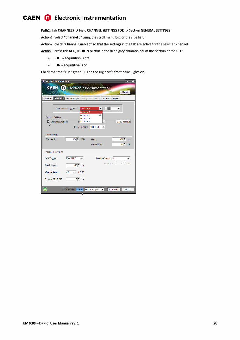
Path2: Tab CHANNELS Field CHANNEL SETTINGS FOR Section GENERAL SETTINGS
Action1: Select “Channel 0” using the scroll menu box or the side bar.
Action2: check “Channel Enabled” so that the settings in the tab are active for the selected channel.
Action3: press the ACQUISITION button in the deep grey common bar at the bottom of the GUI:
OFF = acquisition is off.
ON = acquisition is on.
Check that the “Run” green LED on the Digitizer’s front panel lights on.
CAEN Electronic Instrumentation
29 UM2089 – DPP-CI User Manual rev. 1
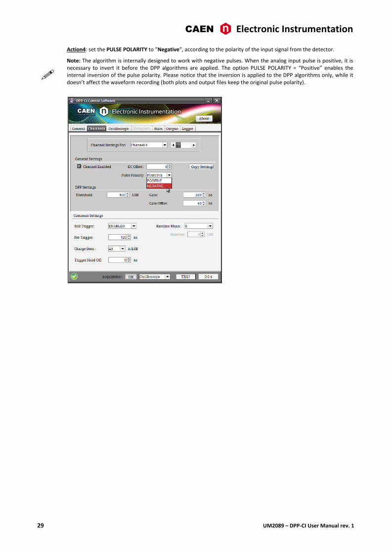
Action4: set the PULSE POLARITY to ”Negative”, according to the polarity of the input signal from the detector.
Note: The algorithm is internally designed to work with negative pulses. When the analog input pulse is positive, it is necessary to invert it before the DPP algorithms are applied. The option PULSE POLARITY = “Positive” enables the internal inversion of the pulse polarity. Please notice that the inversion is applied to the DPP algorithms only, while it doesn’t affect the waveform recording (both plots and output files keep the original pulse polarity).
CAEN Electronic Instrumentation
UM2089 – DPP-CI User Manual rev. 1 30
4. Set the parameters for self-triggering (DC Offset, Baseline, Threshold).
With the acquisition on, since it is not guaranteed that the channel is properly triggering on the input pulses, the Software Trigger is used to force the acquisition. It is so possible to adjust parameters like the DC Offset, the Baseline and the Threshold in order the Digitizer to self-trigger.
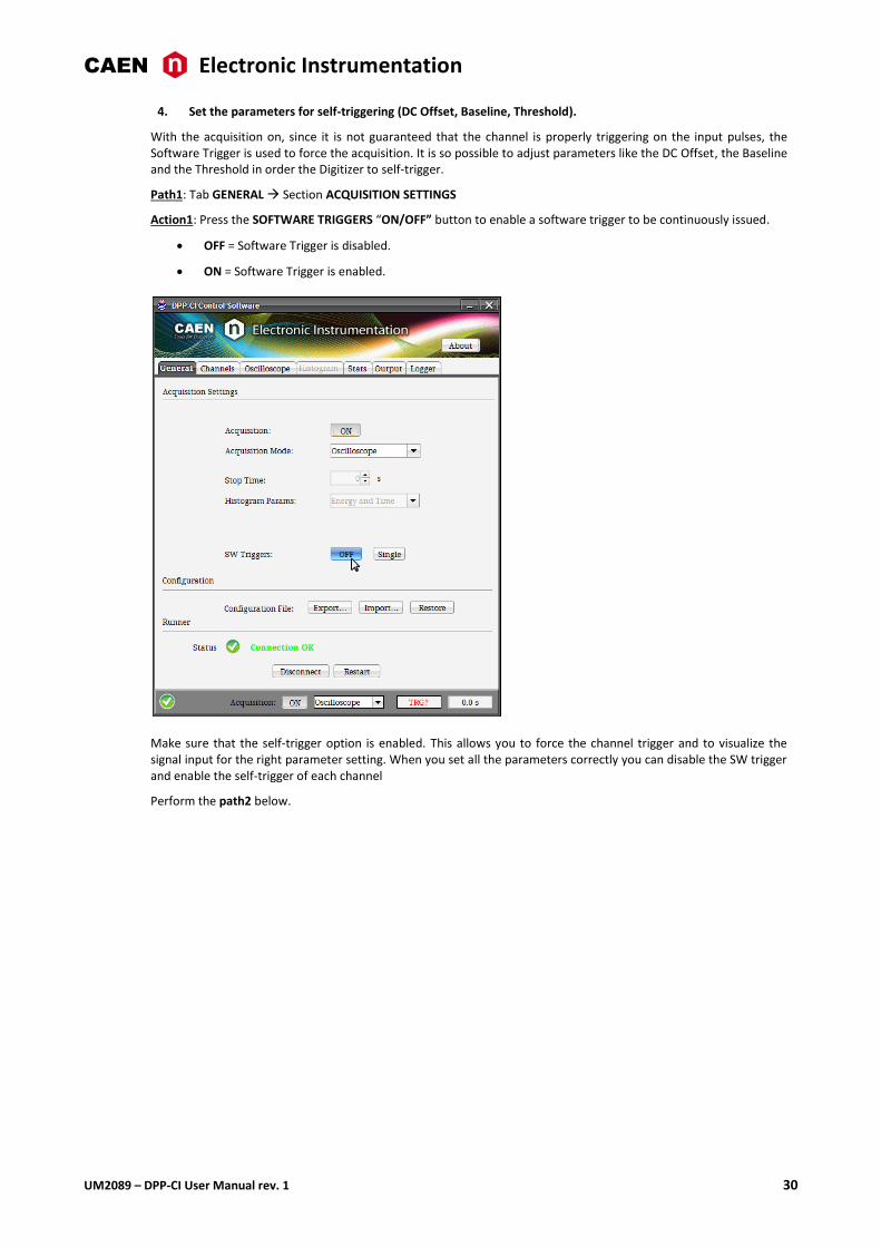
Path1: Tab GENERAL Section ACQUISITION SETTINGS
Action1: Press the SOFTWARE TRIGGERS “ON/OFF” button to enable a software trigger to be continuously issued.
OFF = Software Trigger is disabled.
ON = Software Trigger is enabled.
Make sure that the self-trigger option is enabled. This allows you to force the channel trigger and to visualize the signal input for the right parameter setting. When you set all the parameters correctly you can disable the SW trigger and enable the self-trigger of each channel
Perform the path2 below.
CAEN Electronic Instrumentation
31 UM2089 – DPP-CI User Manual rev. 1
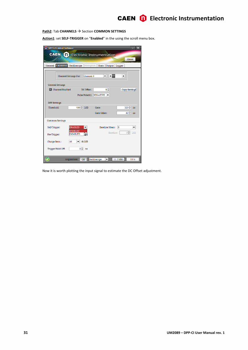
Path2: Tab CHANNELS Section COMMON SETTINGS
Action1: set SELF-TRIGGER on “Enabled” in the using the scroll menu box.
Now it is worth plotting the input signal to estimate the DC Offset adjustment.
CAEN Electronic Instrumentation
UM2089 – DPP-CI User Manual rev. 1 32
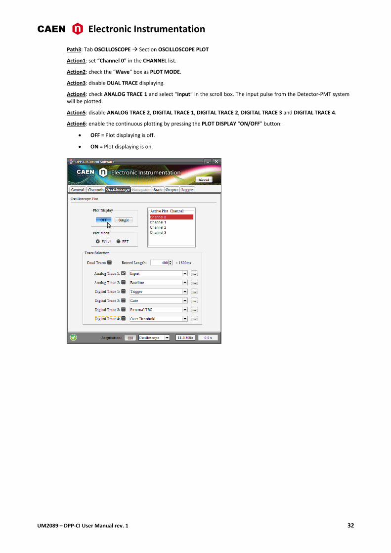
Path3: Tab OSCILLOSCOPE Section OSCILLOSCOPE PLOT
Action1: set “Channel 0” in the CHANNEL list.
Action2: check the “Wave” box as PLOT MODE.
Action3: disable DUAL TRACE displaying.
Action4: check ANALOG TRACE 1 and select “Input” in the scroll box. The input pulse from the Detector-PMT system will be plotted.
Action5: disable ANALOG TRACE 2, DIGITAL TRACE 1, DIGITAL TRACE 2, DIGITAL TRACE 3 and DIGITAL TRACE 4.
Action6: enable the continuous plotting by pressing the PLOT DISPLAY “ON/OFF” button:
OFF = Plot displaying is off.
ON = Plot displaying is on.
CAEN Electronic Instrumentation
33 UM2089 – DPP-CI User Manual rev. 1
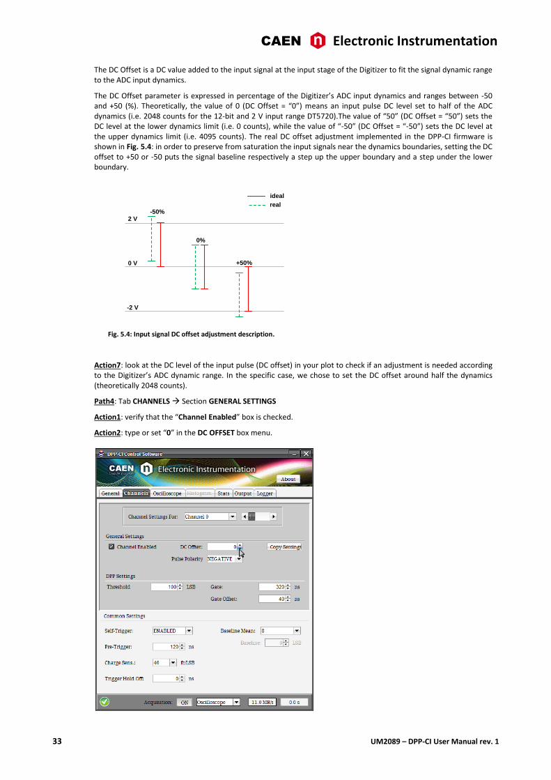
The DC Offset is a DC value added to the input signal at the input stage of the Digitizer to fit the signal dynamic range to the ADC input dynamics.
The DC Offset parameter is expressed in percentage of the Digitizer’s ADC input dynamics and ranges between -50 and +50 (%). Theoretically, the value of 0 (DC Offset = “0”) means an input pulse DC level set to half of the ADC dynamics (i.e. 2048 counts for the 12-bit and 2 V input range DT5720).The value of “50” (DC Offset = “50”) sets the DC level at the lower dynamics limit (i.e. 0 counts), while the value of “-50” (DC Offset = “-50”) sets the DC level at the upper dynamics limit (i.e. 4095 counts). The real DC offset adjustment implemented in the DPP-CI firmware is shown in Fig. 5.4: in order to preserve from saturation the input signals near the dynamics boundaries, setting the DC offset to +50 or -50 puts the signal baseline respectively a step up the upper boundary and a step under the lower boundary.
0 V
2 V
-2 V
ideal
real-50%
0%
+50%
Fig. 5.4: Input signal DC offset adjustment description.
Action7: look at the DC level of the input pulse (DC offset) in your plot to check if an adjustment is needed according to the Digitizer’s ADC dynamic range. In the specific case, we chose to set the DC offset around half the dynamics (theoretically 2048 counts).
Path4: Tab CHANNELS Section GENERAL SETTINGS
Action1: verify that the “Channel Enabled” box is checked.
Action2: type or set “0” in the DC OFFSET box menu.

CAEN Electronic Instrumentation
UM2089 – DPP-CI User Manual rev. 1 34
Action3: check the effect of the previous settings in the plot window.
Note: The plot above has been zoomed. To do that, right click on the plot in a point near the portion of the signal you want to zoom, then release the mouse button, move to a point on the opposite corner and left click. Press “u” key on the keyboard to un-zoom (or press “a” to auto scale).
Next step is to set the input signal baseline calculation. Both the Threshold parameter, i.e. the trigger threshold, and the charge integration are referred to the baseline value.
The Control Software provides two options for setting the baseline:
Baseline mean calculation, where the DPP-CI algorithm calculates online the input signal baseline through a mean filter over a number of samples set by the BASELINE MEAN parameter.
Absolute baseline, where a fixed baseline value is set by the ABSOLUTE BASELINE parameter.
CAEN Electronic Instrumentation
35 UM2089 – DPP-CI User Manual rev. 1
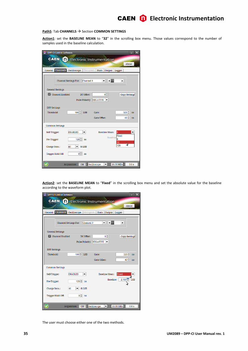
Path5: Tab CHANNELS Section COMMON SETTINGS
Action1: set the BASELINE MEAN to “32” in the scrolling box menu. Those values correspond to the number of samples used in the baseline calculation.
Action2: set the BASELINE MEAN to “Fixed” in the scrolling box menu and set the absolute value for the baseline according to the waveform plot.
The user must choose either one of the two methods.
CAEN Electronic Instrumentation
UM2089 – DPP-CI User Manual rev. 1 36
The plotting of the input signal and the baseline can help to check the effect of the setting.
Path6: Tab OSCILLOSCOPE Section OSCILLOSCOPE PLOT
Action1: enable DUAL TRACE displaying by clicking the related check box. This allows the second analog trace (ANALOG TRACE 2) to be plotted. When you disable the DUAL TRACE setting, the ANALOG TRACE 2 will not be plotted, even if enabled.
Action2: enable ANALOG TRACE 2 check box and select “Baseline” in the scroll menu.
When selecting the automatic baseline calculation the oscilloscope plot will appear as follows:
CAEN Electronic Instrumentation
37 UM2089 – DPP-CI User Manual rev. 1
We choose the first method for the baseline calculation. It is now possible to set the trigger threshold. For this purpose, the parameter THRESHOLD is defined as the relative absolute value of the trigger threshold with respect to the baseline.
The baseline remain frozen for the whole duration of the gate and then it starts again to follow the signal. To freeze it for the whole signal width you must adjust the gate and trigger hold-off parameters. Instructions on how to change those parameters are explained in the following steps.
When choosing the fixed value for the baseline, the baseline remains frozen for the whole acquisition window, as you can see in the following plot.
Note: The oscilloscope plots above has been displayed using the auto scale function of gnuplot (press “a” on your keyboard to activate the auto scale).
CAEN Electronic Instrumentation
UM2089 – DPP-CI User Manual rev. 1 38
Path7: Tab CHANNELS Section1 DPP SETTINGS Section2 COMMON SETTINGS
Action1: set a value of THRESHOLD in the box menu according to the noise level of the input signal baseline. In our example we fix “15” LSB as threshold level.
CAEN Electronic Instrumentation
39 UM2089 – DPP-CI User Manual rev. 1
Path8: Tab GENERAL Section ACQUISITION SETTINGS
Action1: Disable Software Trigger by the “ON/OFF” button. You should observe the board going on self-triggering.
Path9: Tab OSCILLOSCOPE Section OSCILLOSCOPE PLOT
Action2: Enable DIGITAL TRACE 1 and select “Trigger”. Press the “…” button and use the options in the “Trace Settings” window to set the proper digital offset and gain to apply to the trace.
You can check in the plot if the trigger is properly issued.
CAEN Electronic Instrumentation
UM2089 – DPP-CI User Manual rev. 1 40
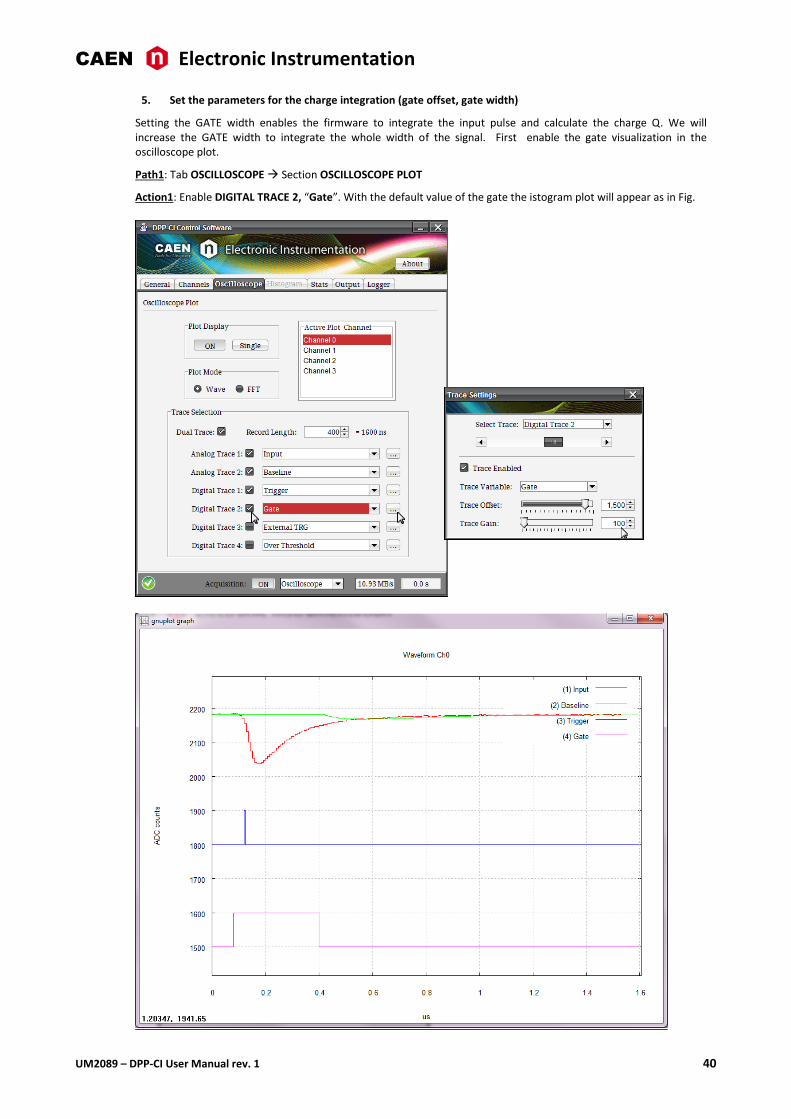
5. Set the parameters for the charge integration (gate offset, gate width)
Setting the GATE width enables the firmware to integrate the input pulse and calculate the charge Q. We will increase the GATE width to integrate the whole width of the signal. First enable the gate visualization in the oscilloscope plot.
Path1: Tab OSCILLOSCOPE Section OSCILLOSCOPE PLOT
Action1: Enable DIGITAL TRACE 2, “Gate”. With the default value of the gate the istogram plot will appear as in Fig.
CAEN Electronic Instrumentation
41 UM2089 – DPP-CI User Manual rev. 1
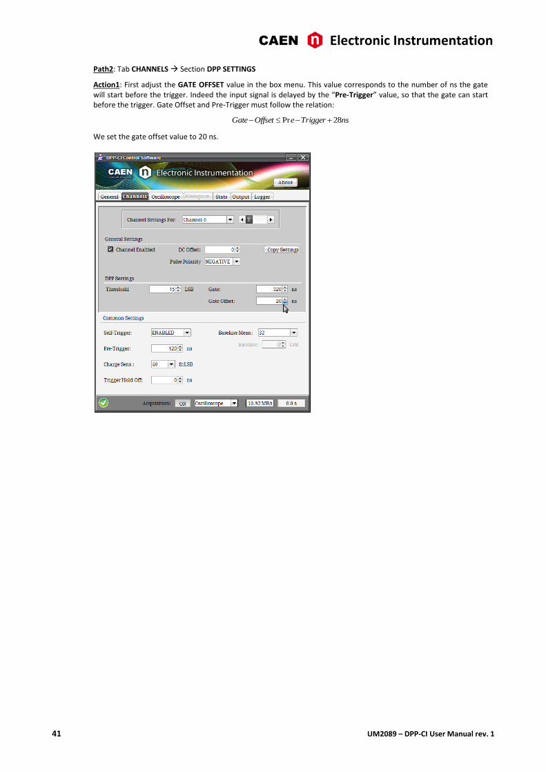
Path2: Tab CHANNELS Section DPP SETTINGS
Action1: First adjust the GATE OFFSET value in the box menu. This value corresponds to the number of ns the gate will start before the trigger. Indeed the input signal is delayed by the “Pre-Trigger” value, so that the gate can start before the trigger. Gate Offset and Pre-Trigger must follow the relation:
nsTriggereOffsetGate 28Pr
We set the gate offset value to 20 ns.
CAEN Electronic Instrumentation
UM2089 – DPP-CI User Manual rev. 1 42
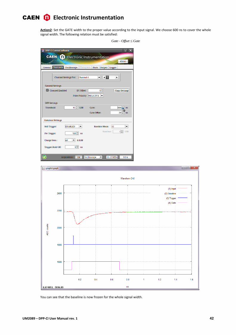
Action2: Set the GATE width to the proper value according to the input signal. We choose 600 ns to cover the whole signal width. The following relation must be satisfied:
GateOffsetGate
You can see that the baseline is now frozen for the whole signal width.
CAEN Electronic Instrumentation
43 UM2089 – DPP-CI User Manual rev. 1
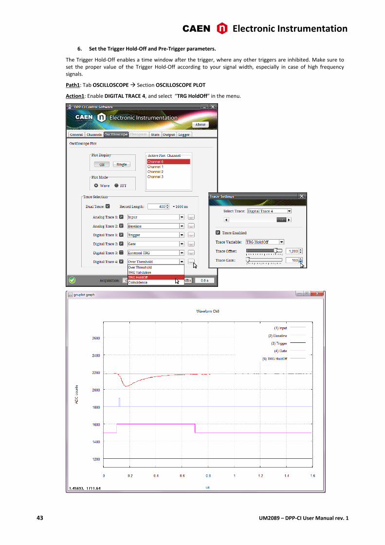
6. Set the Trigger Hold-Off and Pre-Trigger parameters.
The Trigger Hold-Off enables a time window after the trigger, where any other triggers are inhibited. Make sure to set the proper value of the Trigger Hold-Off according to your signal width, especially in case of high frequency signals.
Path1: Tab OSCILLOSCOPE Section OSCILLOSCOPE PLOT
Action1: Enable DIGITAL TRACE 4, and select “TRG HoldOff” in the menu.
CAEN Electronic Instrumentation
UM2089 – DPP-CI User Manual rev. 1 44
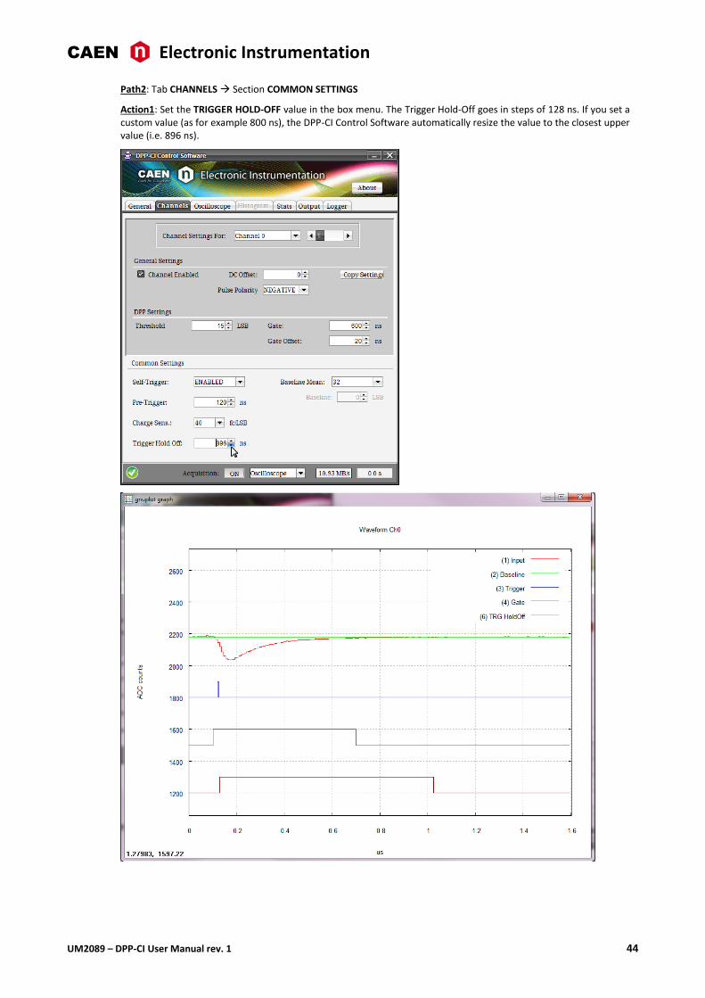
Path2: Tab CHANNELS Section COMMON SETTINGS
Action1: Set the TRIGGER HOLD-OFF value in the box menu. The Trigger Hold-Off goes in steps of 128 ns. If you set a custom value (as for example 800 ns), the DPP-CI Control Software automatically resize the value to the closest upper value (i.e. 896 ns).
CAEN Electronic Instrumentation
45 UM2089 – DPP-CI User Manual rev. 1
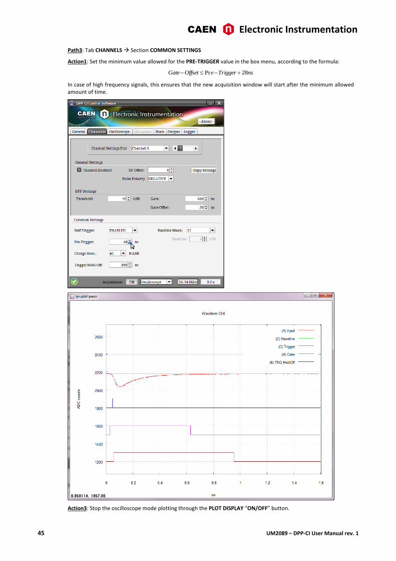
Path3: Tab CHANNELS Section COMMON SETTINGS
Action1: Set the minimum value allowed for the PRE-TRIGGER value in the box menu, according to the formula:
nsTriggereOffsetGate 28Pr
In case of high frequency signals, this ensures that the new acquisition window will start after the minimum allowed amount of time.
Action3: Stop the oscilloscope mode plotting through the PLOT DISPLAY “ON/OFF” button.
CAEN Electronic Instrumentation
UM2089 – DPP-CI User Manual rev. 1 46
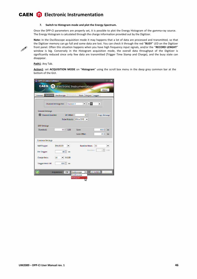
7. Switch to Histogram mode and plot the Energy Spectrum.
Once the DPP-CI parameters are properly set, it is possible to plot the Energy Histogram of the gamma-ray source. The Energy Histogram is calculated through the charge information provided out by the Digitizer.
Note: In the Oscilloscope acquisition mode it may happens that a lot of data are processed and transmitted, so that the Digitizer memory can go full and some data are lost. You can check it through the red “BUSY” LED on the Digitizer front panel. Often this situation happens when you have high frequency input signals, and/or the “RECORD LENGHT” window is big. Conversely in the Histogram acquisition mode, the overall data throughput of the Digitizer is significantly reduced since only few data are transmitted (Trigger Time Stamp and Charge), and the busy state can disappear.
Path1: Any Tab.
Action1: set ACQUISITION MODE on “Histogram” using the scroll box menu in the deep grey common bar at the bottom of the GUI.
CAEN Electronic Instrumentation
47 UM2089 – DPP-CI User Manual rev. 1
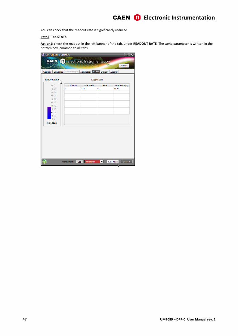
You can check that the readout rate is significantly reduced
Path2: Tab STATS
Action1: check the readout in the left banner of the tab, under READOUT RATE. The same parameter is written in the bottom box, common to all tabs.
CAEN Electronic Instrumentation
UM2089 – DPP-CI User Manual rev. 1 48
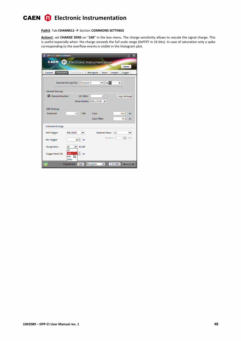
Path3: Tab CHANNELS Section COMMONS SETTINGS
Action1: set CHARGE SENS on “160” in the box menu. The charge sensitivity allows to rescale the signal charge. This is useful especially when the charge exceeds the full scale range (0xFFFF in 16 bits). In case of saturation only a spike corresponding to the overflow events is visible in the histogram plot.
CAEN Electronic Instrumentation
49 UM2089 – DPP-CI User Manual rev. 1
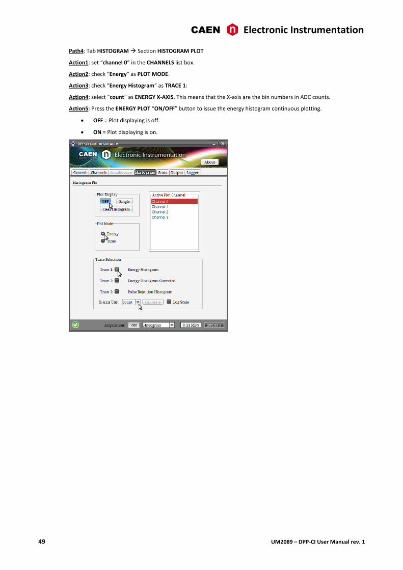
Path4: Tab HISTOGRAM Section HISTOGRAM PLOT
Action1: set “channel 0” in the CHANNELS list box.
Action2: check “Energy” as PLOT MODE.
Action3: check “Energy Histogram” as TRACE 1:
Action4: select “count” as ENERGY X-AXIS. This means that the X-axis are the bin numbers in ADC counts.
Action5: Press the ENERGY PLOT “ON/OFF” button to issue the energy histogram continuous plotting.
OFF = Plot displaying is off.
ON = Plot displaying is on.
CAEN Electronic Instrumentation
UM2089 – DPP-CI User Manual rev. 1 50
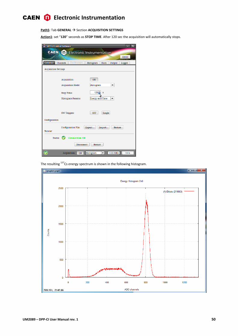
Path5: Tab GENERAL Section ACQUISITION SETTINGS
Action1: set “120” seconds as STOP TIME. After 120 sec the acquisition will automatically stops.
The resulting 137
Cs energy spectrum is shown in the following histogram.
CAEN Electronic Instrumentation
51 UM2089 – DPP-CI User Manual rev. 1
8. Generate the output file and save the Energy Histogram-plot data.
The steps below explain how to save the List file (Time Stamp and Charge) by generating an output file on the host station disk.
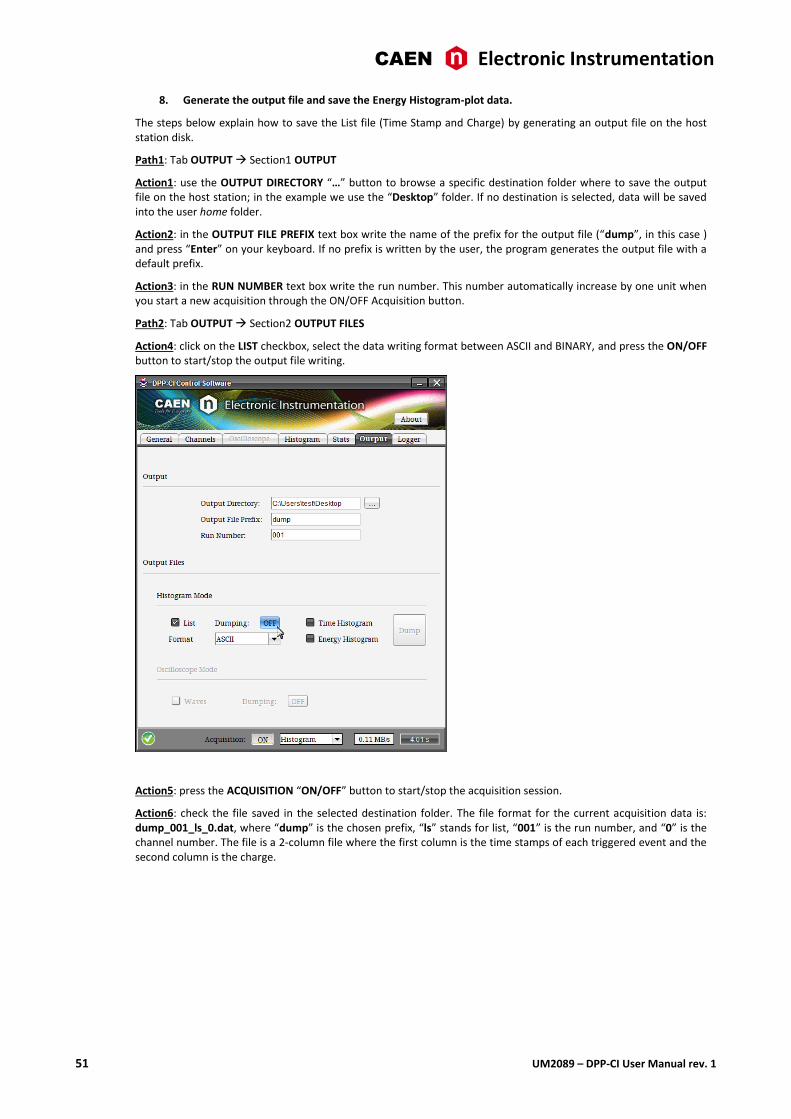
Path1: Tab OUTPUT Section1 OUTPUT
Action1: use the OUTPUT DIRECTORY “…” button to browse a specific destination folder where to save the output file on the host station; in the example we use the “Desktop” folder. If no destination is selected, data will be saved into the user home folder.
Action2: in the OUTPUT FILE PREFIX text box write the name of the prefix for the output file (“dump”, in this case ) and press “Enter” on your keyboard. If no prefix is written by the user, the program generates the output file with a default prefix.
Action3: in the RUN NUMBER text box write the run number. This number automatically increase by one unit when you start a new acquisition through the ON/OFF Acquisition button.
Path2: Tab OUTPUT Section2 OUTPUT FILES
Action4: click on the LIST checkbox, select the data writing format between ASCII and BINARY, and press the ON/OFF button to start/stop the output file writing.
Action5: press the ACQUISITION “ON/OFF” button to start/stop the acquisition session.
Action6: check the file saved in the selected destination folder. The file format for the current acquisition data is: dump_001_ls_0.dat, where “dump” is the chosen prefix, “ls” stands for list, “001” is the run number, and “0” is the channel number. The file is a 2-column file where the first column is the time stamps of each triggered event and the second column is the charge.
CAEN Electronic Instrumentation
UM2089 – DPP-CI User Manual rev. 1 52
6 Coincidences and Synchronization The DPP-CI firmware allows for coincidences among different channels and synchronization of different boards.
Coincidences
Acquiring coincident events from different channels is a common task in physics. Through the DPP firmware each channel of the digitizer can trigger independently from the others, and generate a “trigger request”. All the trigger requests can be sent to the common “ROC FPGA” (see Fig. 1.1) for the coincidence evaluation. The ROC can be programmed to look for triggers within a programmable window, through the Individual Trigger Logic (ITL) that can perform the logic operation of AND, OR, or Majority. When the coincidence condition is met, the ROC sends back a “trigger validation” signal, one per channel. The coincidence logic is individual, so that it is possible to program different coincident conditions for each channel.
The trigger validation enables the data saving into the memory buffer. In this way the channel uses its local trigger for the event building (time stamp, gate, etc..) but only those events having the validation are saved into the memory.
More information and detailed instructions on how to make coincidences among channels of the same board can be found in [RD4].
Synchronization among different boards
In cases when multi-board systems are involved in the experiment, it is necessary to synchronize different boards. In this way the user can acquire from N boards with Y channel each, like if they were just one board with (N x Y) channels.
The main issue in the synchronization of a multi-board system is to propagate the sampling clock among the boards. This can be made by FAN-IN of an external clock into the CLK-IN front panel connector of each board, or, only in case of VME models, propagating in Daisy chain the clock along the digitizers through the CLK-IN / CLK-OUT front panel connectors. One board has to be chosen to be the “master” board that propagates its own clock (internal or external) to the others. A programmable phase shift can adjust possible delays in the clock propagation. This allows to have both the same ADC sampling clock, and the same time reference for all boards. Having the same time reference means that the acquisition starts/stops at the same time, and that the time stamps of different boards is aligned to the same absolute time.
There are several ways to implement the trigger logic. The synchronization tool allows to propagate the trigger to all boards and acquire the events accordingly. Moreover in case of busy state of one or more boards, the acquisition is inhibited for all boards.
Refer to [RD9] for more details on how to synchronize CAEN digitizers.
CAEN Electronic Instrumentation
53 UM2089 – DPP-CI User Manual rev. 1
7 Software Interface Introduction
The DPP-CI Control Software is an application that manages the communication and the data acquisition from digitizers where the DPP-CI firmware is installed. The software allows the user to select proper communication and DPP settings. Waveforms and histograms can also be plotted in real time for one channel at a time (as described in the GUI Description paragraph).
Note: DPP-CI Control Software is not provided with data analysis tools.
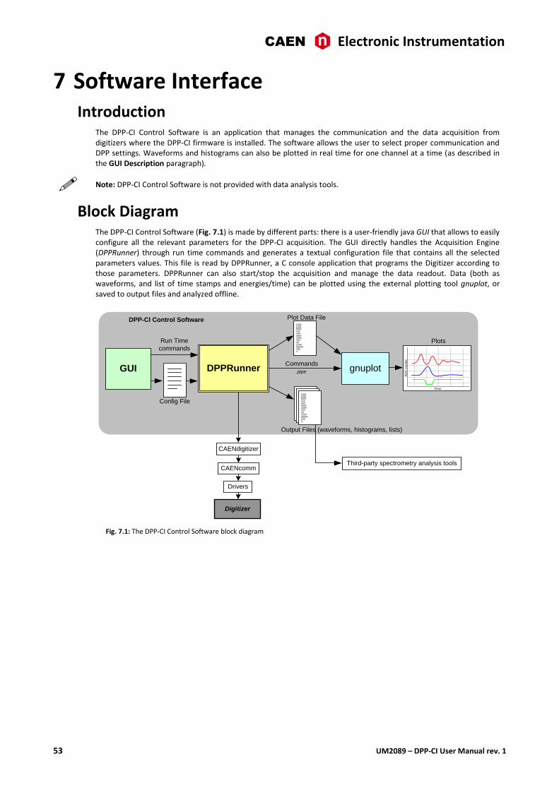
Block Diagram The DPP-CI Control Software (Fig. 7.1) is made by different parts: there is a user-friendly java GUI that allows to easily configure all the relevant parameters for the DPP-CI acquisition. The GUI directly handles the Acquisition Engine (DPPRunner) through run time commands and generates a textual configuration file that contains all the selected parameters values. This file is read by DPPRunner, a C console application that programs the Digitizer according to those parameters. DPPRunner can also start/stop the acquisition and manage the data readout. Data (both as waveforms, and list of time stamps and energies/time) can be plotted using the external plotting tool gnuplot, or saved to output files and analyzed offline.
DPPRunner
Config File
CAENdigitizer
CAENcomm
Drivers
Digitizer
Plot Data File
gnuplotCommands
Time
AD
C c
ou
nts
10231254954412344555673255223442334556432334
Output Files (waveforms, histograms, lists)
10231254954412344555673255223442334556432334
10231254954412344555673255223442334556432334
10231254954412344555673255223442334556432334
Plots
pipeGUI
DPP-CI Control Software
Third-party spectrometry analysis tools
Run Time
commands
Fig. 7.1: The DPP-CI Control Software block diagram
CAEN Electronic Instrumentation
UM2089 – DPP-CI User Manual rev. 1 54
Drivers & Libraries
Drivers
In order to deal with the hardware, CAEN provides the drivers for all the different types of physical communication interfaces featured by the specific digitizer and compliant with Windows and Linux OS:
USB 2.0 Drivers for NIM/Desktop boards are downloadable on CAEN website (www.caen.it) in the “Software/Firmware” tab of the digitizer web page (login required).
Note: Windows OS USB driver installation for Desktop/NIM digitizers is detailed in [RD7].
USB 2.0 Drivers for V1718 CAEN Bridge, required for VME boards interface, is downloadable on CAEN website (www.caen.it) in the “Software/Firmware” tab of the V1718 web page (login required).
Note: For the installation of the V1718 USB driver, refer to the User Manual of the Bridge ([RD11]).
Optical Link Drivers are managed by the A2818 PCI card or the A3818 PCIe card. The driver installation package is available on CAEN website in the “Software/Firmware” area at the A2818 or A3818 page (login required)
Note: For the installation of the Optical Link driver, refer to the User Manual of the specific Controller ([RD12], [RD13]).
Libraries
CAEN libraries are a set of middleware software required by CAEN software tools (including WaveDump) for a correct functioning. These libraries, including also demo and example programs, represent a powerful base for users who want to develop customized applications for the digitizer control (communication, configuration, readout, etc.):
CAENDigitizer is a library of functions designed specifically for the Digitizer family and it supports also the boards running the DPP firmware. The CAENDigitizer library is based on the CAENComm library. For this reason, the CAENComm libraries must be already installed on the host PC before installing the CAENDigitizer.
The CAENDigitizer installation package is available on CAEN website in the ‘Download’ area at the CAENDigitizer Library page. Reference document: [RD6].
CAENComm library manages the communication at low level (read and write access). The purpose of the CAENComm is to implement a common interface to the higher software layers, masking the details of the physical channel and its protocol, thus making the libraries and applications that rely on the CAENComm independent from the physical layer. Moreover, the CAENComm requires the CAENVMELib library (access to the VME bus) even in the cases where the VME is not used. This is the reason why CAENVMELib has to be already installed on your PC before installing the CAENComm.
The CAENComm installation package, and the link to the required CAENVMELib, is available on CAEN website in the ‘Download’ area at the CAENComm Library page. Reference document: [RD14].
CAEN Electronic Instrumentation
55 UM2089 – DPP-CI User Manual rev. 1
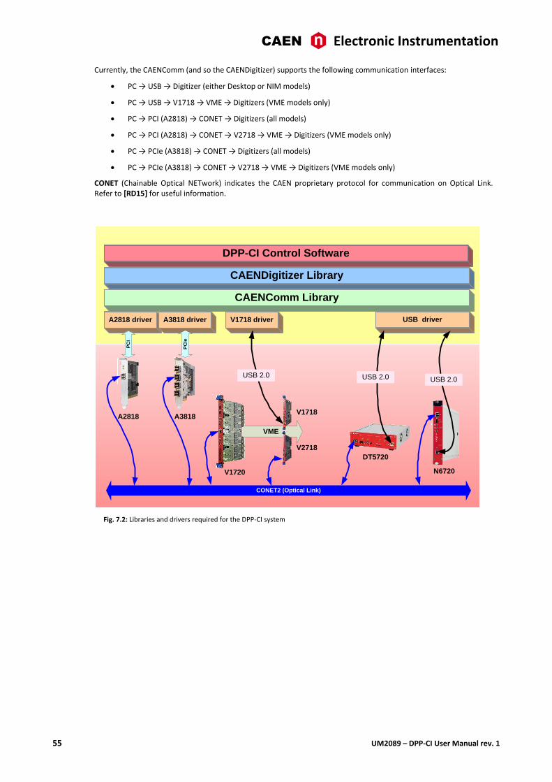
Currently, the CAENComm (and so the CAENDigitizer) supports the following communication interfaces:
PC → USB → Digitizer (either Desktop or NIM models)
PC → USB → V1718 → VME → Digitizers (VME models only)
PC → PCI (A2818) → CONET → Digitizers (all models)
PC → PCI (A2818) → CONET → V2718 → VME → Digitizers (VME models only)
PC → PCIe (A3818) → CONET → Digitizers (all models)
PC → PCIe (A3818) → CONET → V2718 → VME → Digitizers (VME models only)
CONET (Chainable Optical NETwork) indicates the CAEN proprietary protocol for communication on Optical Link. Refer to [RD15] for useful information.
V1720
VME
CONET2 (Optical Link)
DT5720
A2818 A3818
N6720
DPP-CI Control Software
CAENDigitizer Library
CAENComm Library
A2818 driver A3818 driver V1718 driver USB driver
PC
I
PC
Ie
USB 2.0 USB 2.0USB 2.0
V1718
V2718
Fig. 7.2: Libraries and drivers required for the DPP-CI system
CAEN Electronic Instrumentation
UM2089 – DPP-CI User Manual rev. 1 56
Installation In order to manage with DPP-CI system, the host station needs either Windows or Linux OS, and the third-party software Java Runtime Environment 7 or later (trademark of Oracle, Inc, downloadable from http://www.java.com). Linux users must also take care of proper installation of gnuplot graphical tool, as well as of CAEN Libraries. The latter can be downloaded from CAEN website (login required before to download).
Make sure that your hardware (Digitizer and/or Bridge, or Controller) is properly installed (refer to the related User Manual for hardware installation instructions).
Make sure you have installed the driver for your OS and for the communication to be used. Driver installation packages are downloadable on CAEN website (login required before to download) as reported in the Drivers & Libraries section.
CAEN provides the full installation package for the DPP-CI Control Software in a standalone version for Windows OS. This version installs all the binary files required to directly use the software (i.e. no need to install the required CAEN libraries in advance). The installation package for Linux OS needs other libraries to be installed apart.
Download the specific DPP-CI Control Software installation package for your OS from CAEN website in the ‘Download’ area at the DPP-CI Control Software page (login required to download).
Extract files in your host.
For Linux users:
Click on the red link above the DPP-CI Control Software package to download the required CAEN Libraries.
Install the libraries in the following order:
1. CAENVMELib
2. CAENComm
3. CAENDigitizer
The installation instructions can be found in the README file inside each library folder.
Install the DPP-CI Control Software according to the installation instructions of the Setup/Linux/Readme.txt file inside the program folder. Launch the Control Software typing DPP-CI_ControlSoftware
For Windows users
Launch the DPP-CI Control Software installer and complete the Installation Wizard
Run the DPP-CI Control Software GUI by one of the following options:
1. The Desktop icon for the program
2. The Quick Launch icon for the program
3. The .bat file in the main folder from the installation path on your host.
CAEN Electronic Instrumentation
57 UM2089 – DPP-CI User Manual rev. 1
GUI Description The Graphical User Interface (GUI) is composed of seven (7) Tabs, each one divided in one or more sections. In the different tabs there are all the commands needed to manage the connections, to set the board and the channel parameters, and to control the acquisition.
A Common Bar lays at the bottom of the GUI (Fig. 7.3), being visible from any active tab. It contains:
“Acquisition” button: starts and stops the acquisition session.
“Acquisition Mode” menu: sets the “Oscilloscope” or the “Histogram” acquisition mode.
“Readout Rate” box: displays the data throughput rate during the acquisition.
“Time acquisition” box: displays the time duration (sec) of the acquisition. This works only in the Histogram Mode. The acquisition will automatically stop if a “non zero” value is set for the Stop Time parameter.
“Connection” icon: updates itself according to the connection status:
Icon Status
Disconnected
Connection OK
Connection Error
Tab. 7.1: Table of the Connection icon values
Fig. 7.3: Common Bar
Acquisition Time
CAEN Electronic Instrumentation
UM2089 – DPP-CI User Manual rev. 1 58
The Tab “General”
Fig. 7.4: Tab “General”
The General Tab is divided into three sections: Acquisition Settings, Configuration, and Runner.
The Acquisition Settings section includes:
“Acquisition” button: starts and stops the acquisition:
- OFF = acquisition is off
- ON = acquisition is on
It is duplicated in the Common Bar.
“Acquisition Mode” menu: selects between the “Oscilloscope” mode, where the raw waveforms can be visualized and saved, and the “Histogram” mode, where the spectra can be visualized and saved. This command is duplicated in the Common Bar.
“Stop Time” box: sets the value (in seconds) for the Real Time acquisition in Histogram mode. At the end of the fixed time (visualized in the “Acquisition Time” window of the Common Bar) the acquisition is automatically stopped. Set Stop time to “0” for an infinite acquisition time.
“Histogram Params” menu: selects the data that the Digitizer provides for the “Histogram” acquisition mode (Energy only, Energy and Time).
“SW Triggers” buttons: start/stop a software trigger input from the computer to the board in a continuous (“ON/OFF”) or single-shot (“Single”) way.
The Configuration section includes:
“Configuration File” buttons: store (“Export”) and recall (“Import”) the configuration of the software and the parameters for the acquisition. The user can so easily manage the different parameters during different acquisitions. “Restore” resets online the parameters to their default values.
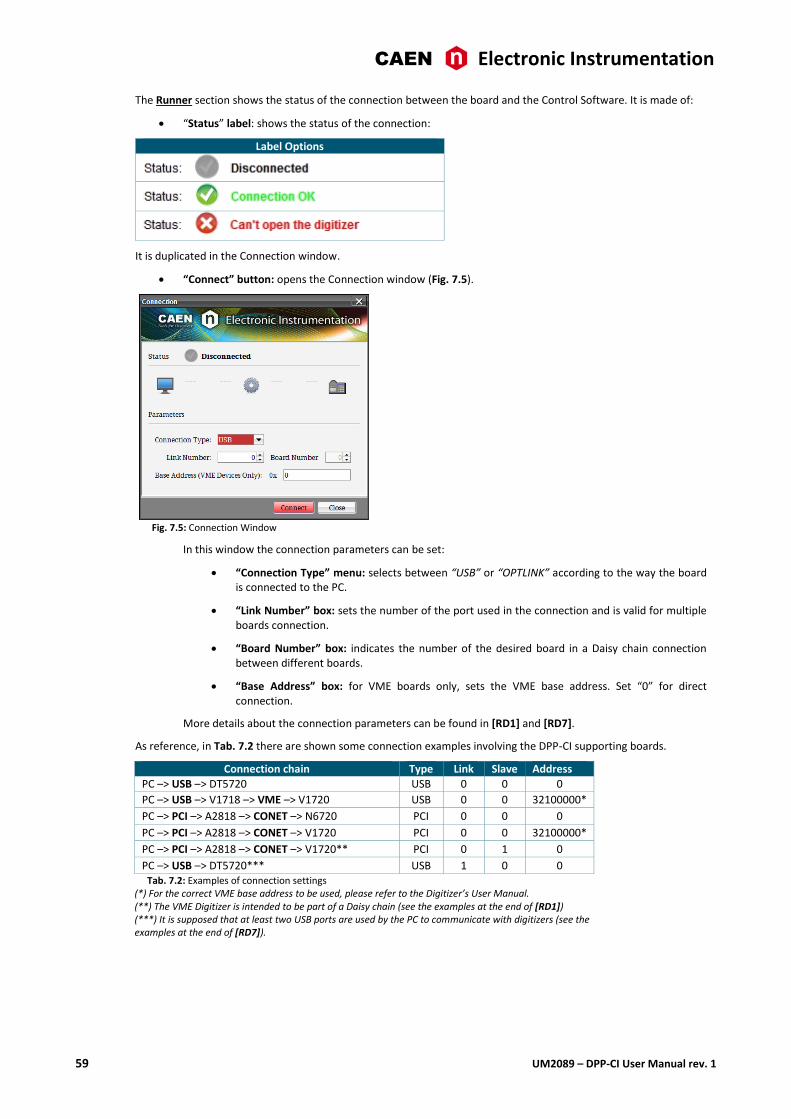
CAEN Electronic Instrumentation
59 UM2089 – DPP-CI User Manual rev. 1
The Runner section shows the status of the connection between the board and the Control Software. It is made of:
“Status” label: shows the status of the connection:
Label Options
It is duplicated in the Connection window.
“Connect” button: opens the Connection window (Fig. 7.5).
Fig. 7.5: Connection Window
In this window the connection parameters can be set:
“Connection Type” menu: selects between “USB” or “OPTLINK” according to the way the board is connected to the PC.
“Link Number” box: sets the number of the port used in the connection and is valid for multiple boards connection.
“Board Number” box: indicates the number of the desired board in a Daisy chain connection between different boards.
“Base Address” box: for VME boards only, sets the VME base address. Set “0” for direct connection.
More details about the connection parameters can be found in [RD1] and [RD7].
As reference, in Tab. 7.2 there are shown some connection examples involving the DPP-CI supporting boards.
Connection chain Type Link Slave Address
PC –> USB –> DT5720 USB 0 0 0
PC –> USB –> V1718 –> VME –> V1720 USB 0 0 32100000*
PC –> PCI –> A2818 –> CONET –> N6720 PCI 0 0 0
PC –> PCI –> A2818 –> CONET –> V1720 PCI 0 0 32100000*
PC –> PCI –> A2818 –> CONET –> V1720** PCI 0 1 0
PC –> USB –> DT5720*** USB 1 0 0 Tab. 7.2: Examples of connection settings
(*) For the correct VME base address to be used, please refer to the Digitizer’s User Manual. (**) The VME Digitizer is intended to be part of a Daisy chain (see the examples at the end of [RD1]) (***) It is supposed that at least two USB ports are used by the PC to communicate with digitizers (see the examples at the end of [RD7]).
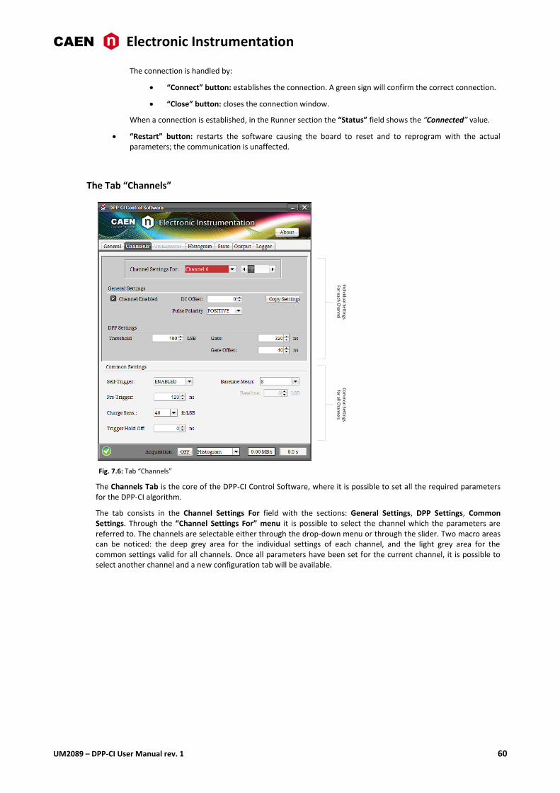
CAEN Electronic Instrumentation
UM2089 – DPP-CI User Manual rev. 1 60
The connection is handled by:
“Connect” button: establishes the connection. A green sign will confirm the correct connection.
“Close” button: closes the connection window.
When a connection is established, in the Runner section the “Status” field shows the “Connected” value.
“Restart” button: restarts the software causing the board to reset and to reprogram with the actual parameters; the communication is unaffected.
The Tab “Channels”
Ind
ividu
al Settings
For each
Ch
ann
elC
om
mo
n Settin
gsfo
r all Ch
ann
els
Fig. 7.6: Tab “Channels”
The Channels Tab is the core of the DPP-CI Control Software, where it is possible to set all the required parameters for the DPP-CI algorithm.
The tab consists in the Channel Settings For field with the sections: General Settings, DPP Settings, Common Settings. Through the “Channel Settings For” menu it is possible to select the channel which the parameters are referred to. The channels are selectable either through the drop-down menu or through the slider. Two macro areas can be noticed: the deep grey area for the individual settings of each channel, and the light grey area for the common settings valid for all channels. Once all parameters have been set for the current channel, it is possible to select another channel and a new configuration tab will be available.

CAEN Electronic Instrumentation
61 UM2089 – DPP-CI User Manual rev. 1
The General Settings section includes the following commands:
“Channel Enabled” checkbox: enables the selected channel to acquire data.
“DC Offset” box: sets the value of the DC Offset applied to the channel, expressed as the percentage of the Full Scale Range. Allowed values range between -50% (Full negative) and +50% (Full Positive). The DC Offset is a DC value added to the input signal by the input stage of the Digitizer in order to fit the signal dynamic range to the ADC input dynamics. Theoretically, the value of 0 (DC Offset = “0”) means that the input pulse DC level is set at half of the ADC dynamics (e.g. 2048 counts for the 720 series). The value of “50” (DC Offset = “50”) sets the DC level at the lower dynamics limit (i.e. 0 counts), while the value of “-50” (DC Offset = “-50”) sets the DC level at the upper dynamics boundary (i.e. 4095). The real DC offset adjustment implemented in the DPP-CI firmware is shown in Fig. 7.7: in order to preserve from saturation the input signals near the dynamics boundaries, setting the DC offset to -50 or +50 puts the signal baseline respectively a step up the upper boundary and a step under the lower boundary.
0 V
2 V
-2 V
ideal
real-50%
0%
+50%
Fig. 7.7: Input signal DC offset adjustment description
“Pulse Polarity” menu: selects the polarity (NEGATIVE/POSITIVE) of the input signal to be processed by the DPP-CI algorithm. The algorithm is internally designed to work with negative pulses. When the analog input pulses are positive, it is necessary to invert them before the DPP algorithm is applied; in this case, the option PULSE POLARITY = “Positive” enables the internal inversion of the pulse polarity. Note that the inversion is applied to the DPP algorithms only, while it doesn’t affect the waveform recording (both plots and output files keep the original pulse polarity). With negative analog input pulses, use PULSE POLARITY = “Negative”.
“Copy Settings” button: copies the general settings of the current channel to other channels.
The DPP Settings section includes:
“Threshold” box: sets the absolute value of the trigger threshold referred to the input pulse baseline. The value is expressed in LSB. The value in mV for 1 LSB can be calculated according to the board input range. For a digitizer of the 720 series, with 12-bit resolution and input range of 2 Volts, the LSB is:
LSB = 2 / 2¹² = 0.488 mV
“Gate” box: sets the gate width parameter for the charge integration of signals. Values are expressed in ns and vary in steps of clock units (i.e. 4 ns).
“Gate Offset” box: sets the “pre-gate” parameter, i.e. the starting position of the gate before the trigger signal. Values are expressed in ns and vary in steps of clock units (4 ns).
CAEN Electronic Instrumentation
UM2089 – DPP-CI User Manual rev. 1 62
The Common Settings section includes:
“Self-Trigger” menu: ENABLE/DISABLE the DPP self-trigger of each channel. When disabled, the DPP algorithm still generates the self-trigger (pulse auto trigger) with the programmed threshold, but the signal is propagated only to the TRG-OUT panel output and not used to make the acquisition. In these conditions, the acquisition is activated by the external trigger signal received on the TRG-IN panel input or by the combination of the other channel self-triggers.
“Pre-Trigger” box: sets the portion of the waveform acquisition window visible before the trigger (i.e. the time, before the trigger when the waveform starts to be saved). It is expressed in ns. The following relation must be true, and it is recommended to set the pre-trigger value to the minimum value allowed:
nsTriggereOffsetGate 28Pr
Note: When switching to histogram mode the Pre-Trigger value is automatically set to the minimum allowed, i.e. Gate-Offset + 28 ns.
“Charge Sens.” Menu: sets the charge sensitivity, the weight of the LSB for the charge data (16 bit). For instance, if Q = 100 is read and Charge Sens. = 40 fC/LSB, the integrated charge is 4 pC. When the charge pulse exceeds the full scale range (0xFFFF), it is recommended to reduce the sensitivity in order to avoid saturation. The allowed values (fC/LSB) are:
40, 160, 640, 2560.
Note: The charge is integrated inside the FPGA over a 22-bit accumulator; the sensitivity defines the dividing factor (i.e. the right shift) of this accumulator to rescale the energy value before it is saved into the memory buffer.
“Trigger Hold-Off” menu: sets the width of a time window after the trigger, where any other triggers are inhibited. It is expressed in steps of 128 ns. Accepted values are:
0, 128, 256, 384, …, 1920.
“Baseline Mean” menu: sets the number of samples used by the mean filter to calculate the input pulse baseline. Allowed values are:
“Fixed”, 8, 32, 128.
The “Fixed” option enables the absolute baseline calculation.
“Baseline” menu: sets the fixed value (in LSB) of the baseline when the “Fixed” value is selected in the “Baseline Mean” menu.
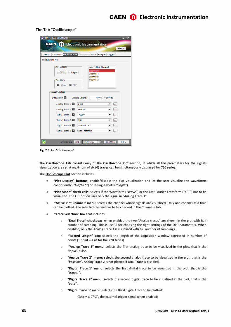
CAEN Electronic Instrumentation
63 UM2089 – DPP-CI User Manual rev. 1
The Tab “Oscilloscope”
Fig. 7.8: Tab “Oscilloscope”
The Oscilloscope Tab consists only of the Oscilloscope Plot section, in which all the parameters for the signals visualization are set. A maximum of six (6) traces can be simultaneously displayed for 720 series.
The Oscilloscope Plot section includes:
“Plot Display” buttons: enable/disable the plot visualization and let the user visualize the waveforms continuously (“ON/OFF”) or in single shots (“Single”).
“Plot Mode” check-cells: selects if the Waveform (“Wave”) or the Fast Fourier Transform (“FFT”) has to be visualized. The FFT option uses only the signal in “Analog Trace 1”.
“Active Plot Channel” menu: selects the channel whose signals are visualized. Only one channel at a time can be plotted. The selected channel has to be checked in the Channels Tab.
“Trace Selection” box that includes:
o “Dual Trace” checkbox: when enabled the two “Analog traces” are shown in the plot with half number of sampling. This is useful for choosing the right settings of the DPP parameters. When disabled, only the Analog Trace 1 is visualized with full number of samplings.
o “Record Length” box: selects the length of the acquisition window expressed in number of points (1 point = 4 ns for the 720 series).
o “Analog Trace 1” menu: selects the first analog trace to be visualized in the plot, that is the “input” pulse.
o “Analog Trace 2” menu: selects the second analog trace to be visualized in the plot, that is the “baseline”. Analog Trace 2 is not plotted if Dual Trace is disabled.
o “Digital Trace 1” menu: selects the first digital trace to be visualized in the plot, that is the “trigger”.
o “Digital Trace 2” menu: selects the second digital trace to be visualized in the plot, that is the “gate”.
o “Digital Trace 3” menu: selects the third digital trace to be plotted:
“External TRG“, the external trigger signal when enabled;
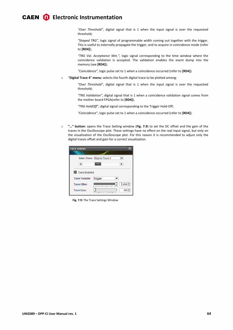
CAEN Electronic Instrumentation
UM2089 – DPP-CI User Manual rev. 1 64
“Over Threshold”, digital signal that is 1 when the input signal is over the requested threshold;
“Shaped TRG”, logic signal of programmable width coming out together with the trigger. This is useful to externally propagate the trigger, and to acquire in coincidence mode (refer to [RD4]);
“TRG Val. Acceptance Win.”, logic signal corresponding to the time window where the coincidence validation is accepted. The validation enables the event dump into the memory (see [RD4]);
“Coincidence“, logic pulse set to 1 when a coincidence occurred (refer to [RD4]).
o “Digital Trace 4” menu: selects the fourth digital trace to be plotted among:
“Over Threshold”, digital signal that is 1 when the input signal is over the requested threshold;
“TRG Validation”, digital signal that is 1 when a coincidence validation signal comes from the mother board FPGA(refer to [RD4]).
“TRG HoldOff”, digital signal corresponding to the Trigger Hold-Off;
“Coincidence“, logic pulse set to 1 when a coincidence occurred (refer to [RD4]).
o “…” button: opens the Trace Setting window (Fig. 7.9) to set the DC offset and the gain of the traces in the Oscilloscope plot. These settings have no effect on the real input signal, but only on the visualization of the Oscilloscope plot. For this reason it is recommended to adjust only the digital traces offset and gain for a correct visualization.
Fig. 7.9: The Trace Settings Window
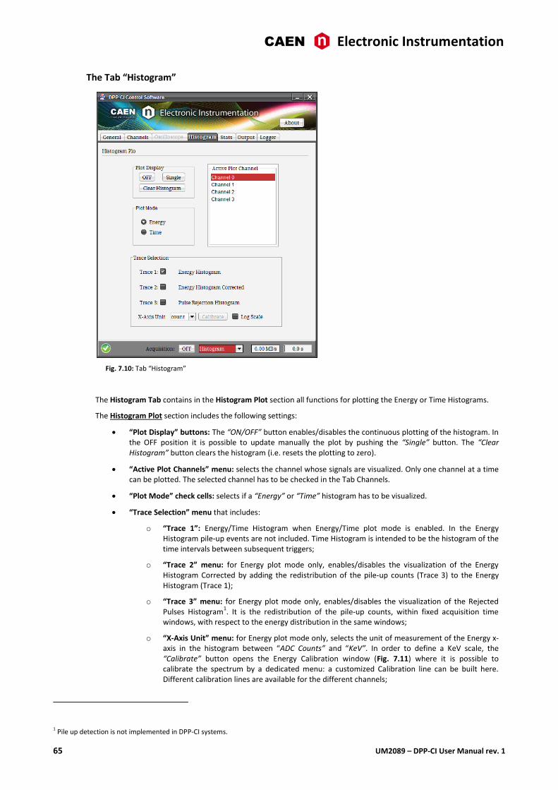
CAEN Electronic Instrumentation
65 UM2089 – DPP-CI User Manual rev. 1
The Tab “Histogram”
Fig. 7.10: Tab “Histogram”
The Histogram Tab contains in the Histogram Plot section all functions for plotting the Energy or Time Histograms.
The Histogram Plot section includes the following settings:
“Plot Display” buttons: The “ON/OFF” button enables/disables the continuous plotting of the histogram. In the OFF position it is possible to update manually the plot by pushing the “Single” button. The “Clear Histogram” button clears the histogram (i.e. resets the plotting to zero).
“Active Plot Channels” menu: selects the channel whose signals are visualized. Only one channel at a time can be plotted. The selected channel has to be checked in the Tab Channels.
“Plot Mode” check cells: selects if a “Energy” or “Time” histogram has to be visualized.
“Trace Selection” menu that includes:
o “Trace 1”: Energy/Time Histogram when Energy/Time plot mode is enabled. In the Energy Histogram pile-up events are not included. Time Histogram is intended to be the histogram of the time intervals between subsequent triggers;
o “Trace 2” menu: for Energy plot mode only, enables/disables the visualization of the Energy Histogram Corrected by adding the redistribution of the pile-up counts (Trace 3) to the Energy Histogram (Trace 1);
o “Trace 3” menu: for Energy plot mode only, enables/disables the visualization of the Rejected Pulses Histogram
1. It is the redistribution of the pile-up counts, within fixed acquisition time
windows, with respect to the energy distribution in the same windows;
o “X-Axis Unit” menu: for Energy plot mode only, selects the unit of measurement of the Energy x-axis in the histogram between “ADC Counts” and “KeV”. In order to define a KeV scale, the “Calibrate” button opens the Energy Calibration window (Fig. 7.11) where it is possible to calibrate the spectrum by a dedicated menu: a customized Calibration line can be built here. Different calibration lines are available for the different channels;
1 Pile up detection is not implemented in DPP-CI systems.
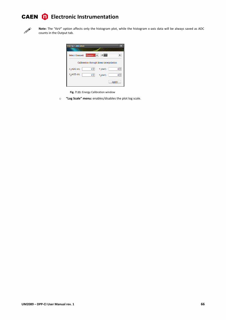
CAEN Electronic Instrumentation
UM2089 – DPP-CI User Manual rev. 1 66
Note: The “KeV” option affects only the histogram plot, while the histogram x-axis data will be always saved as ADC counts in the Output tab.
Fig. 7.11: Energy Calibration window
o “Log Scale” menu: enables/disables the plot log scale.
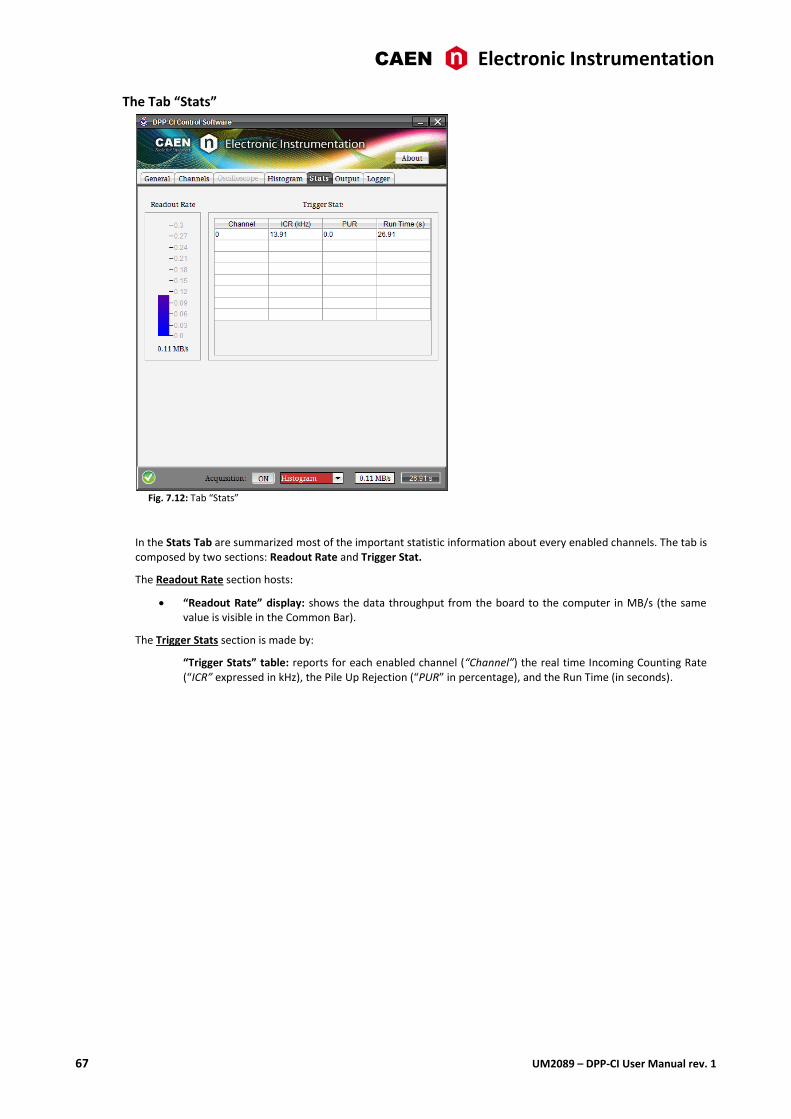
CAEN Electronic Instrumentation
67 UM2089 – DPP-CI User Manual rev. 1
The Tab “Stats”
Fig. 7.12: Tab “Stats”
In the Stats Tab are summarized most of the important statistic information about every enabled channels. The tab is composed by two sections: Readout Rate and Trigger Stat.
The Readout Rate section hosts:
“Readout Rate” display: shows the data throughput from the board to the computer in MB/s (the same value is visible in the Common Bar).
The Trigger Stats section is made by:
“Trigger Stats” table: reports for each enabled channel (“Channel”) the real time Incoming Counting Rate (“ICR” expressed in kHz), the Pile Up Rejection (“PUR” in percentage), and the Run Time (in seconds).
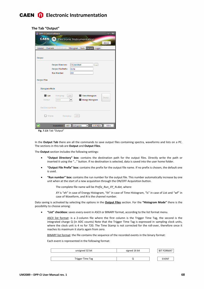
CAEN Electronic Instrumentation
UM2089 – DPP-CI User Manual rev. 1 68
The Tab “Output”
Fig. 7.13: Tab “Output”
In the Output Tab there are all the commands to save output files containing spectra, waveforms and lists on a PC. The sections in this tab are Output and Output Files.
The Output section includes the following settings:
“Output Directory” box: contains the destination path for the output files. Directly write the path or inserted it using the “…” button. If no destination is selected, data is saved into the user home folder.
“Output File Prefix” box: contains the prefix for the output file name. If no prefix is chosen, the default one is used.
“Run number” box: contains the run number for the output file. This number automatically increase by one unit when at the start of a new acquisition through the ON/OFF Acquisition button.
The complete file name will be Prefix_Run_XY_N.dat, where:
XY is “eh” in case of Energy Histogram, “th” in case of Time Histogram, “ls” in case of List and “wf” in case of Waveform, and N is the channel number.
Data saving is activated by selecting the options in the Output Files section. For the “Histogram Mode” there is the possibility to choose among:
“List” checkbox: saves every event in ASCII or BINARY format, according to the list format menu.
ASCII list format: is a 2-column file where the first column is the Trigger Time Tag, the second is the integrated charge Q (in ADC counts) Note that the Trigger Time Tag is expressed in sampling clock units, where the clock unit is 4 ns for 720. The Time Stamp is not corrected for the roll-over, therefore once it reaches its maximum it starts again from zero.
BINARY list format: the file contains the sequence of the recorded events in the binary format:
Each event is represented in the following format:
BIT FORMATunsigned 32 bit signed 16 bit
EVENTTrigger Time Tag Q
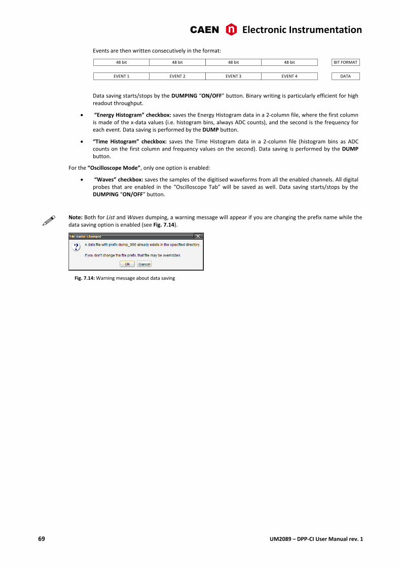
CAEN Electronic Instrumentation
69 UM2089 – DPP-CI User Manual rev. 1
Events are then written consecutively in the format:
BIT FORMAT48 bit48 bit
DATAEVENT 4EVENT 3EVENT 2EVENT 1
48 bit48 bit
Data saving starts/stops by the DUMPING “ON/OFF” button. Binary writing is particularly efficient for high readout throughput.
“Energy Histogram” checkbox: saves the Energy Histogram data in a 2-column file, where the first column is made of the x-data values (i.e. histogram bins, always ADC counts), and the second is the frequency for each event. Data saving is performed by the DUMP button.
“Time Histogram” checkbox: saves the Time Histogram data in a 2-column file (histogram bins as ADC counts on the first column and frequency values on the second). Data saving is performed by the DUMP button.
For the “Oscilloscope Mode”, only one option is enabled:
“Waves” checkbox: saves the samples of the digitised waveforms from all the enabled channels. All digital probes that are enabled in the “Oscilloscope Tab” will be saved as well. Data saving starts/stops by the DUMPING “ON/OFF” button.
Note: Both for List and Waves dumping, a warning message will appear if you are changing the prefix name while the data saving option is enabled (see Fig. 7.14).
Fig. 7.14: Warning message about data saving
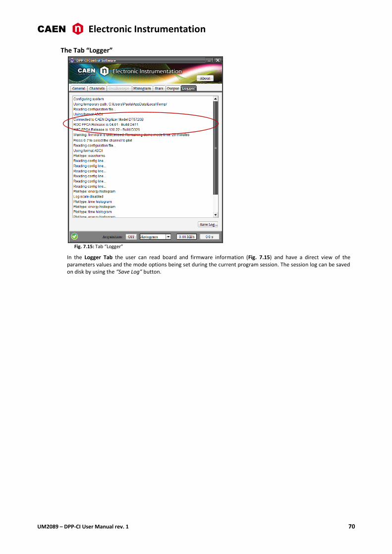
CAEN Electronic Instrumentation
UM2089 – DPP-CI User Manual rev. 1 70
The Tab “Logger”
Fig. 7.15: Tab “Logger”
In the Logger Tab the user can read board and firmware information (Fig. 7.15) and have a direct view of the parameters values and the mode options being set during the current program session. The session log can be saved on disk by using the “Save Log” button.

CAEN Electronic Instrumentation
71 UM2089 – DPP-CI User Manual rev. 1
Config File Sintax The Graphical User Interface (GUI) interacts with the board through a Configuration File which is modified by the GUI itself. Moreover, in the configuration file there are some advanced controls that are not present in the GUI. Acting in the different sections of the Configuration File makes possible to enable/disable/modify these features. In this section there is a brief description of the Configuration File and of the Syntax used.
The Configuration File is a text file called DPPRunnerConfig.txt generated by the program in a different destination path according to the user.
Here follows some examples of typical paths for different Operating Systems:
Windows: %HomePath%\AppData\Local\DPP-CI_ControlSoftware\DppRunnerConfig.txt
Where in
Windows XP: %HomePath% is C:\Documents and Settings\<USER>
Windows 7: %HomePath% is C:\Users\<USER>
Linux: /home/<USER>/.DPP-CI_ControlSoftware/DppRunnerConfig.txt
Note: this is the Configuration file that has to be used for enabling/disabling/modifying the GUI controls.
The safer procedure to modify the Configuration File is:
1. Disconnect the board via GUI
2. Modify the Configuration File
3. Save the Configuration File
4. Connect the board via GUI
5. Start acquisition
The Configuration File is divided in two (2) sections: COMMON and INDIVIDUAL.
Common Settings are listed in the file after the [COMMON] keyword and they are in common to all the channels of the Digitizer.
Individual Settings are the ones related to a single channel of the Digitizer. Each list of individual parameters set for
the same channel has to be reported after a [i] keyword, where “i” is the number of the channel section:
[0]
ENABLE_INPUT YES # setting 1 of channel “0” section
DC_OFFSET 40 # setting 2 of channel “0” section
[1]
ENABLE_INPUT NO # setting 1 of channel “1” section
DC_OFFSET 40 # setting 1 of channel “1” section
Each parameter not present in the Individual Settings section is intended to assume the value defined in the Common Settings section.
Each command has a description where there are shown the different options to modify it. The commands are textual so it is very easy to modify the different parameters.

CAEN Electronic Instrumentation
UM2089 – DPP-CI User Manual rev. 1 72
Example 1: Enabling the External Trigger with no propagation
Go in the # EXTERNAL_TRIGGER section and modify the EXTERNAL TRIGGER line from:
EXTERNAL_TRIGGER DISABLED
to
EXTERNAL_TRIGGER ACQUISITION_ONLY
In this way the board will be ready to accept an external trigger.
Other commands must be modified with numerical values and, in this case, the units are expressed in the description.
Example 2: Setting the Pre-Trigger value
# PRE_TRIGGER: pre trigger size in number of samples
# options: 1 to 511
The relative command line will therefore be:
PRE_TRIGGER 500
In the Configuration File is even possible to manually modify the registers of the board within the Write Register section. For more details about the registers refer to the specific x720 User Manual and [RD5].
A copy of the Configuration File can be found in the “data” folder of the program and it is called DPPRunnerConfigDefault.txt. This file contains the default values for all parameters and it is read by the GUI when the Restore button is pushed.
At the same destination path of the DPPRunnerConfig.txt, another file is generated by the program, that is the GuiConfig.txt: this contains the structure definition of the GUI (not to be modified by the user) and a section with the trace parameters shown in Fig. 7.9 (Trace Offset and Trace Gain).
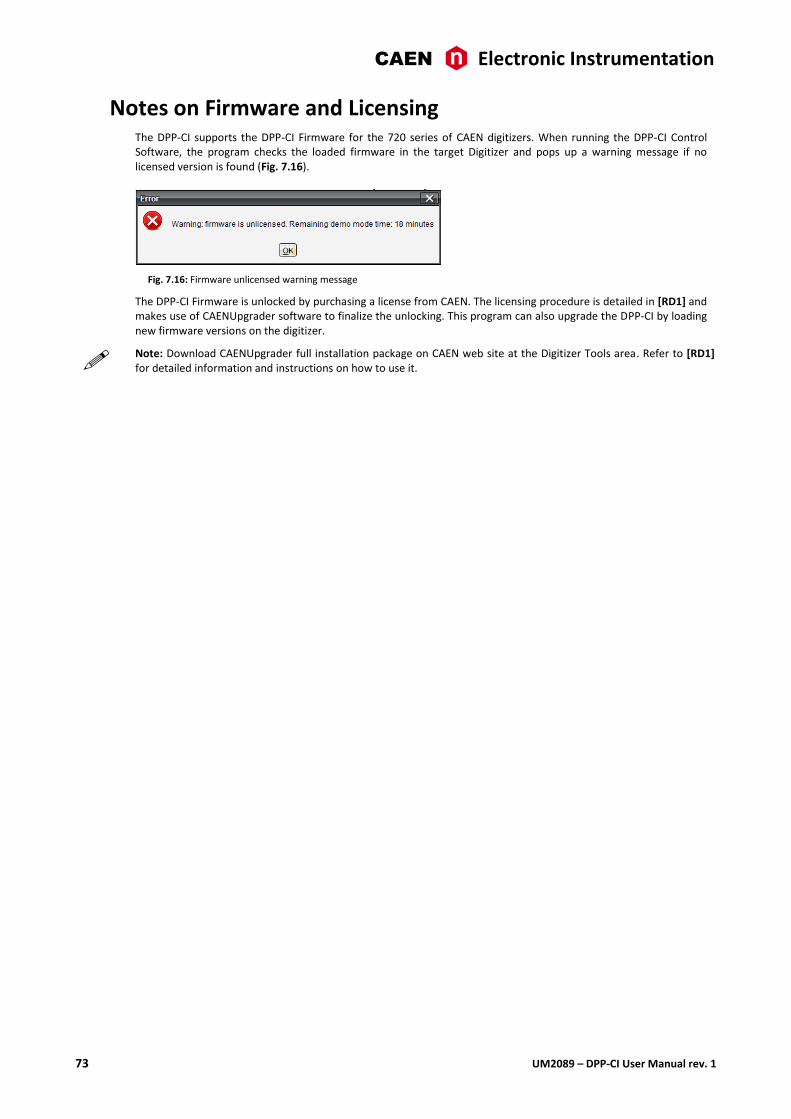
CAEN Electronic Instrumentation
73 UM2089 – DPP-CI User Manual rev. 1
Notes on Firmware and Licensing The DPP-CI supports the DPP-CI Firmware for the 720 series of CAEN digitizers. When running the DPP-CI Control Software, the program checks the loaded firmware in the target Digitizer and pops up a warning message if no licensed version is found (Fig. 7.16).
Fig. 7.16: Firmware unlicensed warning message
The DPP-CI Firmware is unlocked by purchasing a license from CAEN. The licensing procedure is detailed in [RD1] and makes use of CAENUpgrader software to finalize the unlocking. This program can also upgrade the DPP-CI by loading new firmware versions on the digitizer.
Note: Download CAENUpgrader full installation package on CAEN web site at the Digitizer Tools area. Refer to [RD1] for detailed information and instructions on how to use it.

CAEN Electronic Instrumentation
UM2089 – DPP-CI User Manual rev. 1 74
8 Technical support CAEN makes available the technical support of its specialists at the e-mail addresses below:
[email protected] (for questions about the hardware)
(for questions about software and libraries)
CAEN Tools for Discovery
n
Electronic Instrumentation
75 UM2089 – DPP-CI User Manual rev. 1
CAEN SpA is acknowledged as the only company in the world providing a complete range of High/Low Voltage Power Supply systems and Front-End/Data Acquisition modules which meet IEEE Standards for Nuclear and Particle Physics. Extensive Research and Development capabilities have allowed CAEN SpA to play an important, long term role in this field. Our activities have always been at the forefront of technology, thanks to years of intensive collaborations with the most important Research Centres of the world. Our products appeal to a wide range of customers including engineers, scientists and technical professionals who all trust them to help achieve their goals faster and more effectively.
CAEN S.p.A. CAEN GmbH CAEN Technologies, Inc.
Via Vetraia, 11 Klingenstraße 108 1140 Bay Street - Suite 2 C
55049 Viareggio D-42651 Solingen Staten Island, NY 10305
Italy Germany USA
Tel. +39.0584.388.398 Tel. +49 (0)212 254 4077 Tel. +1.718.981.0401
Fax +39.0584.388.959 Mobile +49 (0)151 16 548 484 Fax +1.718.556.9185
[email protected] Fax +49 (0)212 25 44079 [email protected]
www.caen.it [email protected] www.caentechnologies.com
www.caen-de.com
CAEN Tools for Discovery
Electronic Instrumentation
UM2089 – DPP-CI User Manual rev.1 - 21 April 2015
00117-10-DGT28-MUTX
Copyright © CAEN SpA. All rights reserved. Information in this publication supersedes all earlier versions. Specifications subject to change without notice.