calculation of the electrostatic field distribution formed ...ceur-ws.org/vol-1904/paper18.pdf ·...
TRANSCRIPT
3rd International conference “Information Technology and Nanotechnology 2017” 93
Calculation of the electrostatic field distribution formed by the generator of
the off-electrode plasma
M.A. Markushin1, V.A. Kolpakov
1, S.V. Krichevskiy
1
1Samara National Research University, 34 Moskovskoe Shosse, 443086, Samara, Russia
Abstract
A calculation of the electrostatic field distribution in the electrode system of a high-voltage gas-discharge device is made. The application of
the conformal mapping method in order to obtain an analytical description of the of equipotentials and field lines distribution is described. The
figures of the electrostatic field distribution are calculated, which made it possible to determine their relationship with the cathode-anode
distance, the voltage at the electrodes and the hole diameter in the anode of the gas discharge device. The electrostatic field distribution of the
device forming the off-electrode plasma is analyzed.
Keywords: plasma; high-voltage gas discharge; equipotentials; field lines; conformal mapping; the Schwarz-Christoffel integral
1. Introduction
The off-electrode gas-discharge plasma formed by a high-voltage gas discharge is used for plasmachemical etching of quartz,
for preparing Ohmic contacts of semiconductor elements, cleaning the surfaces of semiconductor and dielectric substrates,
contacts of small-size relays [1-4]. The high uniformity of the charged particles flow in the region of the gas discharge cross
section and the independence of the discharge parameters from the dimensions of the treated area [5, 6] causes the wide
propagation of this discharge. These advantages are a consequence of the singularity of the lines of the force and equipotentials
distribution of the off-electrode plasma generator [7-9]. In turn, of the electrostatic field distribution depending on the design
parameters determines the physics of the charged particles interaction processes with atoms and molecules of the residual gas.
Existing publications contain no information on the relationship between such parameters and the electrostatic field distribution.
Due with the laboriousness of the experimental study of this problem the computational model is proposed for the field
distribution in the electrode system of a gas-discharge device.
2. Calculation of electrostatic field distribution of the off-electrode plasma generator
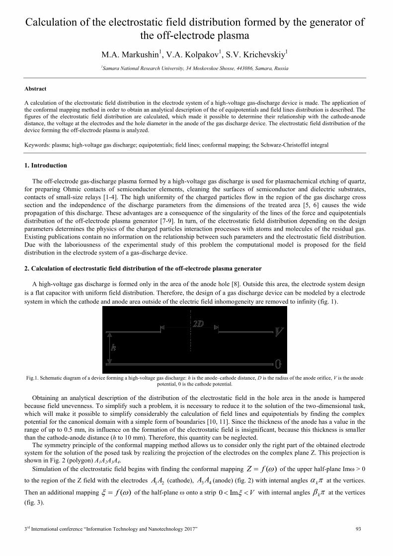
A high-voltage gas discharge is formed only in the area of the anode hole [8]. Outside this area, the electrode system design
is a flat capacitor with uniform field distribution. Therefore, the design of a gas discharge device can be modeled by a electrode
system in which the cathode and anode area outside of the electric field inhomogeneity are removed to infinity (fig. 1).
Fig.1. Schematic diagram of a device forming a high-voltage gas discharge: h is the anode–cathode distance, D is the radius of the anode orifice, V is the anode
potential, 0 is the cathode potential.
Obtaining an analytical description of the distribution of the electrostatic field in the hole area in the anode is hampered
because field unevenness. To simplify such a problem, it is necessary to reduce it to the solution of the two-dimensional task,
which will make it possible to simplify considerably the calculation of field lines and equipotentials by finding the complex
potential for the canonical domain with a simple form of boundaries [10, 11]. Since the thickness of the anode has a value in the
range of up to 0.5 mm, its influence on the formation of the electrostatic field is insignificant, because this thickness is smaller
than the cathode-anode distance (h to 10 mm). Therefore, this quantity can be neglected.
The symmetry principle of the conformal mapping method allows us to consider only the right part of the obtained electrode
system for the solution of the posed task by realizing the projection of the electrodes on the complex plane Z. This projection is
shown in Fig. 2 (polygon) А1А2А3А4.
Simulation of the electrostatic field begins with finding the conformal mapping )(fZ of the upper half-plane Im > 0
to the region of the Z field with the electrodes 21AA (cathode), 43AA (anode)
(fig. 2) with internal angles k at the vertices.
Then an additional mapping )( f of the half-plane onto a strip
V Im0 with internal angles k at the vertices
(fig. 3).

Mathematical Modeling / M.A. Markushin, V.A. Kolpakov, S.V. Krichevskiy
3rd International conference “Information Technology and Nanotechnology 2017” 94
Fig.2. Diagram of the half-plane mapping onto plane (the electrode system).
Fig.3. Diagram of the additional mapping of the half-plane Im > 0 onto the strip V Im0 .
At the first stage, the vertices 4321 AAAA of the Z-plane are associated with certain points of the real axis of the plane .
According to the theorem of uniqueness of a conformal mapping for a present correspondence of three arbitrarily chosen
boundary points, for example, 0, 1, ∞, we can obtain the correspondence [11]:
2
4321
10 a
AAAA
.
According to the technique developed in [10-12], the angles μk are determined, which complement the internal angles αk at
the vertices of the quadrangle 4321 AAAA to π. Considering the inner region of a quadrilateral and moving in the positive
direction of traversing its boundary, i.e. counterclockwise, we find the angles: 2/11 )2/11( 11 ;
12
);01( 22 13 )21( 33 ; 2/34 )2/11( 44 .
To find the mapping function of a domain bounded by a polygon 4321 AAAA
the Schwarz-Christoffel integral [11] is used:
,)...()()( 1
11
2
1
121
1
0
CdaaaCZ n
n
(1)
In the expression (1) instead of а1 – an we substitute the corresponding points 0, 1, а2, ∞. According to [10], the factor related
to the vertex а4 in the Schwarz-Christoffel integral is omitted, since а4 = ∞.
In this case, the expression (1) has the form:
0
1
2
1
0
212
1
11 Cd
aСCdaСZ
Let 2x , then:
.1
1ln12
)1(
)(1
2
0
1
2
2
22
CaCСCdxxx
axCZ
(2)
The value of the constant coefficient 1C is determined from the correspondence of the points 1A ↔ 0, which allows us to
write the equation:

Mathematical Modeling / M.A. Markushin, V.A. Kolpakov, S.V. Krichevskiy
3rd International conference “Information Technology and Nanotechnology 2017” 95
001
01ln)1(02 11
2
CCaCCZ .
The transition from the lower electrode to the upper one, corresponding to the transition of the ray А1А2 to the ray А2А3 (fig.
2), allows us to determine the constants a2 and C. As a result, the function receives an increment:
.ihZ (3) In addition, with such a small increment Δω, the increment of the first term in (2) is also small because of the continuity of
this term at ω = 1. Taking into account that the argument varies from π to 0 as we go around the point ω = 1, the increment of
the second term has the form:
.)ln()ln(1
1ln
irer i
This allows us to write the expression:
).)(1(]1
1ln)1(2[lim 22
0
iaCaCCZ r
reri
(4)
Equating (3) and (4), we obtain:
.12 iaСih
Thus, the change of the coefficient value 2a can be described by the equation:
.12
С
ha
(5)
The correspondence of the points 2a and А3 makes it possible to transform expression (2) to the form:
i
h
a
ah
a
ha
a
ah
a
haihD
1
1ln
1
2
1
1ln
1
222
,
1
1ln
1
22 a
ah
a
haD
.
Whence we obtain the following equality:
.1
1
1
2exp
2
a
a
a
a
hD
(6)
Given specific values of D = 0.9 mm, h = 1.2 mm, we can obtain a solution of the transcendental equation (6) and find the
value of the constant 179.42 a . Substituting it in (5), we obtain
24.0С mm.
As a result, the function realizing the conformal mapping of the half-plane ω onto the plane Z has the form:
.1
1ln2
hСZ
(7)
Thus, expressions (5), (6) allow us to find a constant C whose value depends on the design parameters D and h.
At the second stage, an additional mapping of the half-plane Im > 0 is applied to the strip V Im0 with cuts along the
corresponding rays (fig. 3). In this case we have a capacitor with infinite plates in the plane .
Considering only the right triangle with vertices В1В2В3 because of the electrode design symmetry, we put the points 0, 1, ∞
lying on the real axis ω in correspondence to these vertices [11]:
10
321 BBB
. The inner angles
k at the vertices of the triangle В1В2В3 and the angles '
k , that complement the angles k to π, are defined
similarly to αk, µk,: 1'
2 )01( '
22 ; 2/1'
3 )2/11( '
33 ; 2/1'
1 )2/11( '
11 .
The obtained values ,2/1,0,2/1 321 ensure equality
.13
1
i
i , which confirms the correctness of the sought
angles values according to [11].
An additional conformal mapping is also determined by the Schwarz-Christoffel integral [10]:
.)1(
)1(0 0
32
12/1
2
C
dCdС
The introduction of the new variable ω=u
2 allows us to obtain the solution of the given integral:

Mathematical Modeling / M.A. Markushin, V.A. Kolpakov, S.V. Krichevskiy
3rd International conference “Information Technology and Nanotechnology 2017” 96
.1
1ln
)1(2C
0
32322
CCC
uu
udu
(8)
From the correspondence of the points B1↔ 0 according to the technique outlined above, there is a constant С3.
,001
01ln 332 CCC
.03 C
The constant С2 is defined similarly to the constant C in the first stage, namely, by traversal of the point ω = 1, we get the
increment
.iV
Since the increment of the argument changes from π to 0 upon traversal of the above point, the increment of function ξ
corresponds to the expression:
,)(]1
1ln[lim 222
0
iCiCC r
reri
which allows us to obtain equality:
.2 iCiV
Solving this equality, we define 2C :
.2
VC
The final function conformally mapping the half-plane to the strip V Im0 has the form:
.2
1
1ln
arcth
VV
(9)
Using (7) and (9), we obtain a system of equations:
arcthV
Lnh
СZ
2
1
12
(10)
From (10) we find
.2
2
21
21
ln2
2
V
h
VthС
Vth
Vth
h
VthСZ
(11)
By separating the real and imaginary parts of equation (11), the parametric equations of lines of equal potential and field lines
of force are found. After separation, we obtain a system of equations describing the coordinates of the electric field distribution
in the electrode system of a gas-discharge device:
.
cos
sin
2
cos
2
V
v
V
uch
V
v
CV
hvy
V
v
V
uch
V
ush
СV
hux
(12)
Substituting the parameters h, V, D into the expressions (5), (6) and system (12) and changing the values of the variables v
and u with the necessary step, we can determine the number of the field lines and equipotential distribution (fig.4 and fig.5).
Changing the voltage at the electrodes does not lead to a change in the field configuration, but it affects the energy of charged
particles. Thus, the equations system (12) allows to obtain the electrode system configuration to form the required electric field
by varying the parameters h, V, D.

Mathematical Modeling / M.A. Markushin, V.A. Kolpakov, S.V. Krichevskiy
3rd International conference “Information Technology and Nanotechnology 2017” 97
Fig.4. Field lines and equipotentials distribution in the electrode system of the gas-discharge device obtained by the equations system (12): a – h = 2.7 mm,
D = 1 mm, V = 1200 V; b – h = 2.7 mm, D = 3 mm, V = 1200 V; c – h = 2.7 mm, D = 5 mm, V = 1200 V.
3. Analysis of the field lines and equipotentials distribution
The initial coordinate (x = x0, y = y0 = 0) of the rectilinear segment of the field line can be determined with the aid of the
system (12), giving the values u = u0 and v0 = 0. Then, searching further all the values of v = v1-vn for which the coordinate x = x0
is constant, and the y varies in the limits y1-yn. Further on, comparing the obtained maximum value of yn with the mean free path
of the electron kλе (k = 1,2,3) and the potential at the given point with the ionization energy of the working gas atom (molecule)
Ei, we verify the fulfillment of the condition for the emergence of an high-voltage discharge γQ ≥ 1 [ 8] is, where γ is the number
of electrons knocked by one ion from the cathode (γ-process), Q is the number of positive ions formed by the electron on the
trajectory of its motion due to inelastic collisions with atoms and molecules of the working gas (α-process). The energy
c
a
b

Mathematical Modeling / M.A. Markushin, V.A. Kolpakov, S.V. Krichevskiy
3rd International conference “Information Technology and Nanotechnology 2017” 98
accumulated by the electron on the mean free path must be higher than the ionization energy of the working gas atom, and the
energy of the positive ion bombarding the cathode must be sufficient for the emission of electrons necessary for sustaining the
self-dependent discharge. Analogously, changing the values u = u1-un for v0 = 0, the corresponding x = x1-xn are determined.
Further on, searching further values of v = v1-vn for each x, we find y = y1-yn = 0-kλе. In other words, by repeating the
comparison process, we can find all field lines with initial coordinates e
xx ,...,0, on the rectilinear segments of which the
ionization process takes place (α-process), and, accordingly, the length of the cathode regionexx 2 where the electron
emission from the cathode (γ-process) takes place [13].
Fig.5. Field lines and equipotentials distribution in the electrode system of the gas-discharge device obtained by the equations system (12): a – h = 1 mm,
D = 3 mm, V = 1200 V; b – h = 2.7 mm, D = 3 mm, V = 1200 V; c – h = 4 mm, D = 3 mm, V = 1200 V.
a
b
c

Mathematical Modeling / M.A. Markushin, V.A. Kolpakov, S.V. Krichevskiy
3rd International conference “Information Technology and Nanotechnology 2017” 99
In order to compare the maximum values of yn with kλe, it is necessary to find the mean free path of an electron. Using the
expression λe = 1/(Ni) [14], we obtain the value 0.203 cm, which makes it possible to determine 318x μm. The
calculated value of x correlated well with the experimental data of [9], namely, the size of the region on the cathode surface
with intense sputtering by positive ions is 300 μm (fig. 6).
Fig 6. The profile of the etching pit on the surface of the cathode formed by positive ions.
This value is comparable with the size of the region x on which the rectilinear segments of field lines correspond to the value
kλе and the condition for the emergence of an high-voltage discharge is observed.
4. Conclusions
The parametric equations system presented in this paper makes it possible to simulate the of the field lines and equipotentials
distribution in the electrode system of the off-electrode plasma generator and to monitor the dependence of this distribution on
the design parameters of the system: the anode-cathode distance, the hole diameter in the anode, and also on the applied voltage
at the electrodes. In addition, estimates are made in this paper: the length of the rectilinear segments of the field lines on which
the condition is satisfied, the size of the cathode spot x within which the γ process is realized. The discrepancy between the
calculated value and the experimental value does not exceed 6%, which indicates that the model corresponds to the actual
physical processes occurring in the electrode system of a high-voltage gas discharge. Therefore, it becomes possible to optimize
the devices design forming the off-electrode plasma without costly experimental investigations.
Acknowledgments
This work was supported by grants from the President of the Russian Foundation for State Support of Young Russian Ph.D.
Scientists (MD-5205.2016.9) and the Russian Foundation for Basic Research (project no. 16-07-00494 A).
References
[1] Komov AN, Kolpakov AI, Bondareva NI, Zakharenko VV. Electron-beam unit for soldering semiconductor devices. Instruments and Experimental
Techniques 1984; 5: 218-220.
[2] Kazanskiy NL, Kolpakov VA, Kolpakov AI. Investigation of the features of the anisotropic etching of silicon dioxide in plasma high-voltage gas
discharge. Microelectronics 2004; 33(3): 209-224.
[3] Kolpakov VA, Kolpakov AI, Krichevskiy SV. Ion-plasma cleaning of the low-power relay contacts surface. Elektronnaya promyshlennost 1996; 2: 41–
44.
[4] Kazanskiy NL, Kolpakov VA, Krichevskiy SV. Simulation of the cleaning process the surface of dielectric substrates in plasma formed by high-voltage
gas discharge. Computer Optics 2005; 28: 80–86.
[5] Kazanskiy NL, Kolpakov VA. Investigation of the mechanisms of low-temperature plasma formation by a high-voltage gas discharge. Computer Optics
2003; 25: 112–116.
[6] Kazanskiy NL, Kolpakov VA, Kolpakov AI, Krichevskiy SV. Gas discharge devices forming directed flows of the off-electrode plasma. Part I. Nauchnoe
priborostroenie 2012; 22(1): 13–18.
[7] Soifer VA, Kazanskiy NL, Kolpakov VA, Kolpakov AI. Patent 2333619 Russian Federation, MPK Н 05 Н 1/24. Multi-beam gas-discharge plasma
generator. Applicant and patent holder IPSI RAS N 2006121061; declared 13.06.06; published 10.09.08, bulletin. N 25; 5 p.
[8] Kazanskiy NL, Kolpakov VA. Formation of an optical microrelief in off-electrode high-voltage gas discharge plasma. M .: Radio and Communications,
2009; 220 p.
[9] Kolpakov VA, Kolpakov AI, Podlipnov VV. Formation of the off-electrode plasma in a high-voltage gas discharge. Technical Physics 2013; 83(4): 41–46.
[10] Miroljubov NN, Kostenko MV, Levinshtejn ML, Tihodeev NN. Calculation methods of electrostatistic fields. M.: Vysshaja Shkola, 1963; 415 p.
[11] Lavrent'ev MA, Shabat BV. Methods of the theory of functions of a complex variable / M.A. Lavrent'ev. M.: Nauka, 1973; 736 p.
[12] Novgorodtsev AB, Fethiev AR, Fethieva IS. Application of complex variable function to calculation of electrostatic fields of irregular shape electrodes: a
tutorial. Ufa: Ufimskij ordena Lenina aviacionnyj institut im. Sergo Ordzhonikidze, 1986; 82 p.
[13] Raizer YuP. Gas discharge physics. M.: Nauka, 1987; 592 p.
[14] Kudryavtsev AA, Smirnov AС, Tsendin LD. Physics of glow discharge: a tutorial. SPb.: Lan', 2010; 512 p.