cambridge university napoli university isie, dubrovnik, june 21st 2005 accurate physical model for...
Post on 20-Dec-2015
213 views
TRANSCRIPT

ISIE, Dubrovnik, June 21st 2005CAMBRIDGEUNIVERSITY
NAPOLI
UNIVERSITY
Accurate Physical Model for the Lateral IGBT in Silicon On Insulator Technology
Ettore Napoli1,2, Vasantha Pathirana1, Florin Udrea1,3
1 Dept. of Engineering, University of Cambridge, UK2 Dept. Electronic and Telecom. Univ. of Napoli, Italy3 Cambridge Semiconductor (CamSemi), UK
EU research program ROBUSPIC
ISIE, Dubrovnik, June 21st 2005CAMBRIDGEUNIVERSITY
NAPOLI
UNIVERSITY
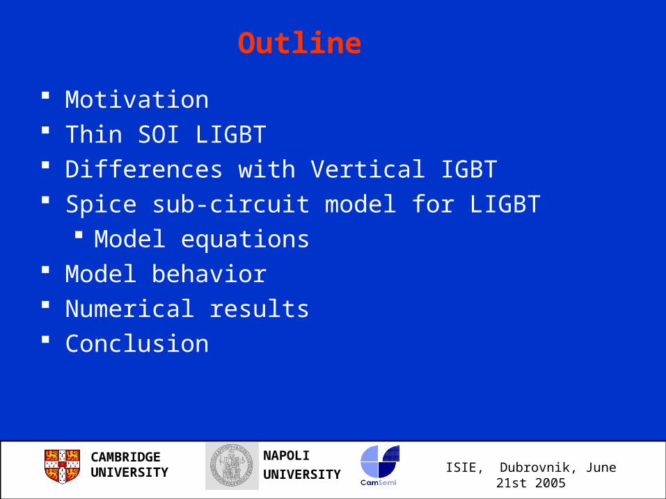
Outline
Motivation Thin SOI LIGBT Differences with Vertical IGBT Spice sub-circuit model for LIGBT
Model equations Model behavior Numerical results Conclusion
ISIE, Dubrovnik, June 21st 2005CAMBRIDGEUNIVERSITY
NAPOLI
UNIVERSITY
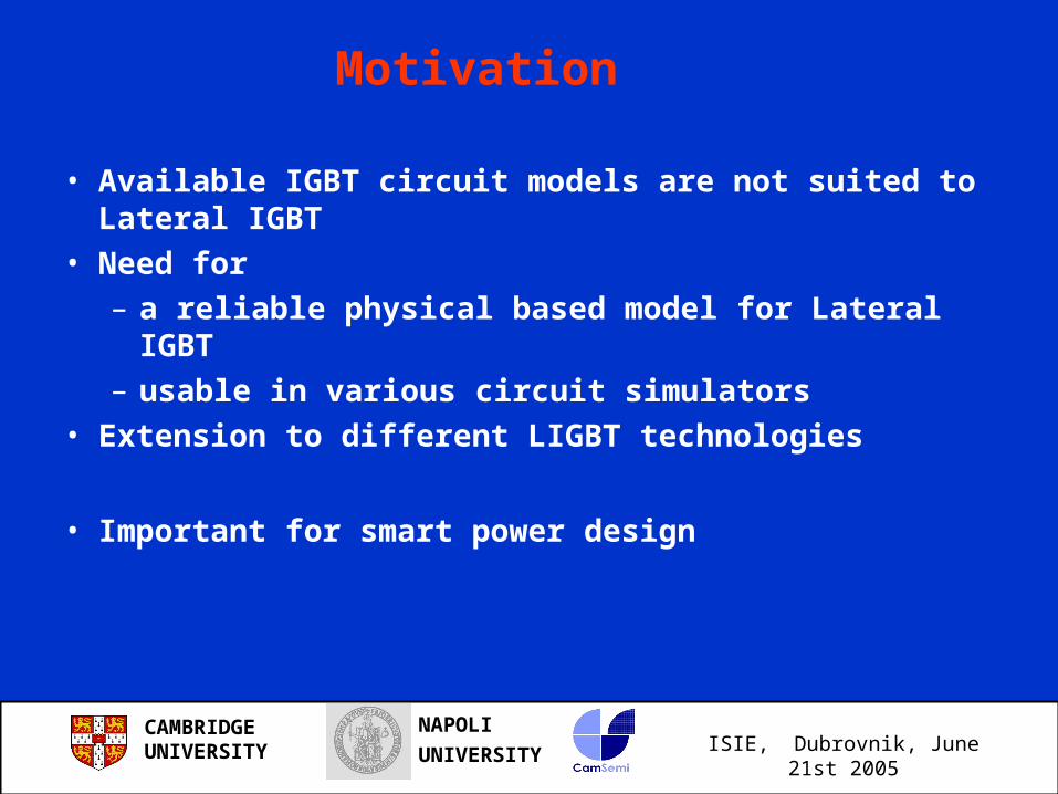
Motivation
• Available IGBT circuit models are not suited to Lateral IGBT
• Need for– a reliable physical based model for Lateral IGBT– usable in various circuit simulators
• Extension to different LIGBT technologies
• Important for smart power design
ISIE, Dubrovnik, June 21st 2005CAMBRIDGEUNIVERSITY
NAPOLI
UNIVERSITY
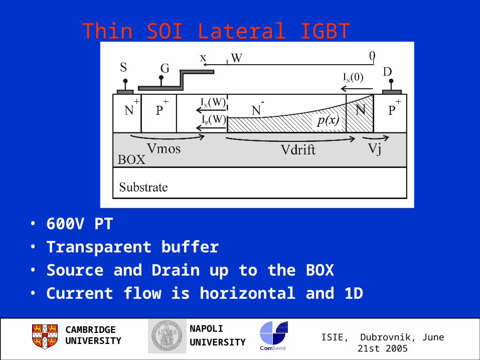
Thin SOI Lateral IGBT
• 600V PT• Transparent buffer• Source and Drain up to the BOX• Current flow is horizontal and 1D
ISIE, Dubrovnik, June 21st 2005CAMBRIDGEUNIVERSITY
NAPOLI
UNIVERSITY
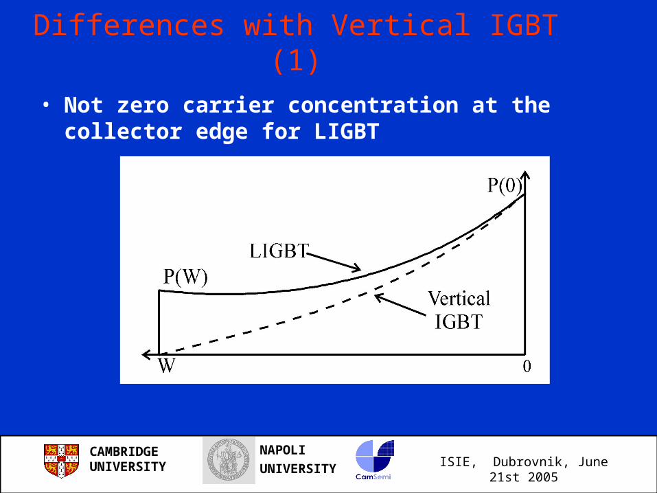
Differences with Vertical IGBT (1)
• Not zero carrier concentration at the collector edge for LIGBT
ISIE, Dubrovnik, June 21st 2005CAMBRIDGEUNIVERSITY
NAPOLI
UNIVERSITY
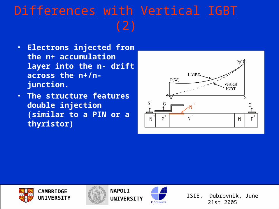
Differences with Vertical IGBT (2)
• Electrons injected from the n+ accumulation layer into the n- drift across the n+/n- junction.
• The structure features double injection (similar to a PIN or a thyristor)
N+
N+G DS
NN-
P+
P+
ISIE, Dubrovnik, June 21st 2005CAMBRIDGEUNIVERSITY
NAPOLI
UNIVERSITY
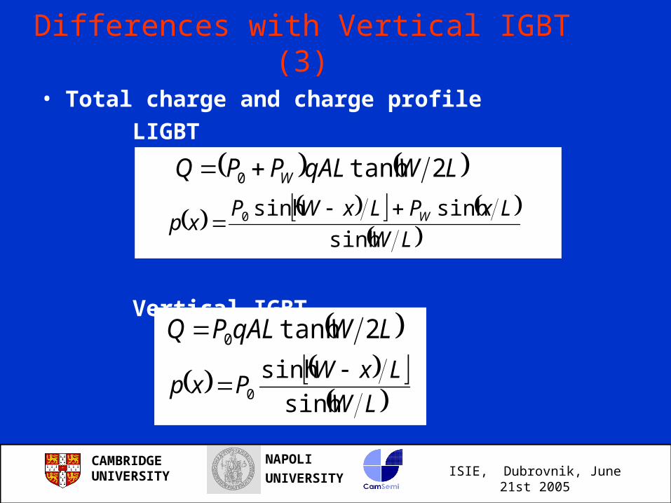
• Total charge and charge profile
LIGBT
Vertical IGBT
LW
LxPLxWPxp W
sinh
sinhsinh0
LWqALPPQ W 2tanh0
LW
LxWPxp
sinh
sinh0
LWqALPQ 2tanh0
Differences with Vertical IGBT (3)
ISIE, Dubrovnik, June 21st 2005CAMBRIDGEUNIVERSITY
NAPOLI
UNIVERSITY
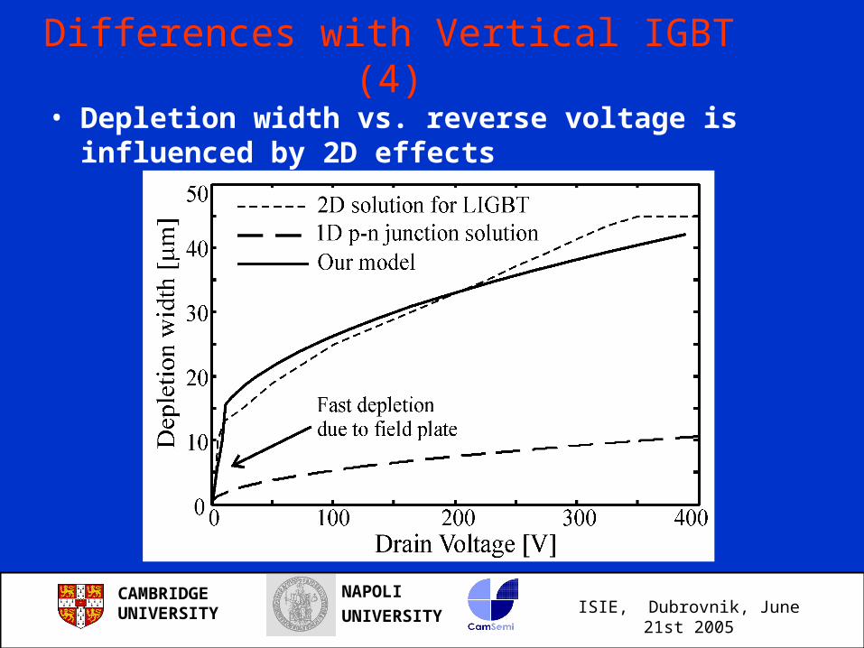
Differences with Vertical IGBT (4)
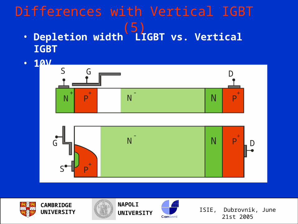
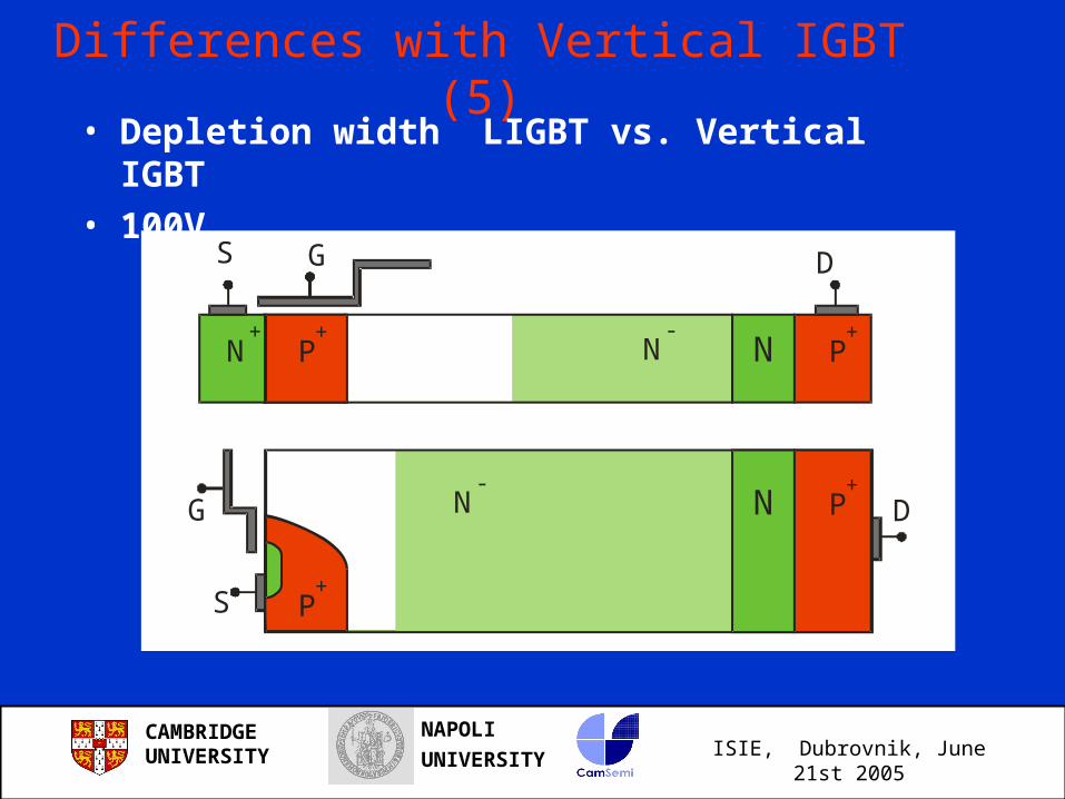
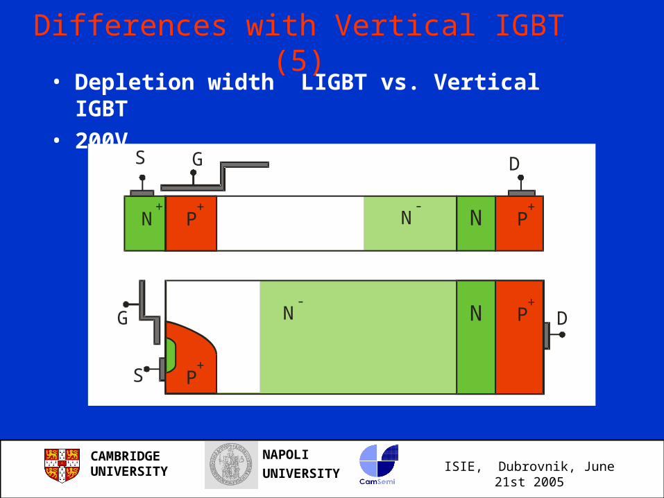
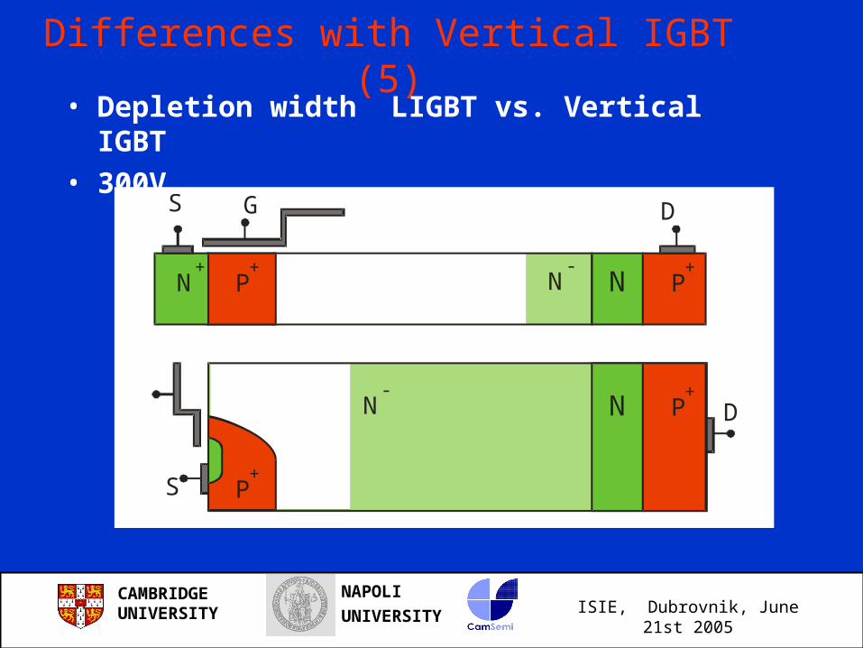
• Depletion width vs. reverse voltage is influenced by 2D effects
ISIE, Dubrovnik, June 21st 2005CAMBRIDGEUNIVERSITY
NAPOLI
UNIVERSITY
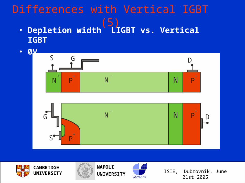
Differences with Vertical IGBT (5)• Depletion width LIGBT vs. Vertical IGBT• 0V
N+
G
G
D
D
S
S
NN-
P+
P+
NN-
P+
P+

ISIE, Dubrovnik, June 21st 2005CAMBRIDGEUNIVERSITY
NAPOLI
UNIVERSITY
Differences with Vertical IGBT (5)• Depletion width LIGBT vs. Vertical IGBT• 5V
N+
G
G
D
D
S
S
NN-
P+
P+
NN-
P+
P+
ISIE, Dubrovnik, June 21st 2005CAMBRIDGEUNIVERSITY
NAPOLI
UNIVERSITY
Differences with Vertical IGBT (5)• Depletion width LIGBT vs. Vertical IGBT• 10V
N+
G
G
D
D
S
S
NN-
P+
P+
NN-
P+
P+
ISIE, Dubrovnik, June 21st 2005CAMBRIDGEUNIVERSITY
NAPOLI
UNIVERSITY
Differences with Vertical IGBT (5)• Depletion width LIGBT vs. Vertical IGBT• 100V
N+
G
G
D
D
S
S
NN-
P+
P+
NN-
P+
P+
ISIE, Dubrovnik, June 21st 2005CAMBRIDGEUNIVERSITY
NAPOLI
UNIVERSITY
Differences with Vertical IGBT (5)• Depletion width LIGBT vs. Vertical IGBT• 200V
N+
G
G
D
D
S
S
NN-
P+
P+
NN-
P+
P+
ISIE, Dubrovnik, June 21st 2005CAMBRIDGEUNIVERSITY
NAPOLI
UNIVERSITY
Differences with Vertical IGBT (5)• Depletion width LIGBT vs. Vertical IGBT• 300V
N+
G D
D
S
S
NN-
P+
P+
NN-
P+
P+
ISIE, Dubrovnik, June 21st 2005CAMBRIDGEUNIVERSITY
NAPOLI
UNIVERSITY
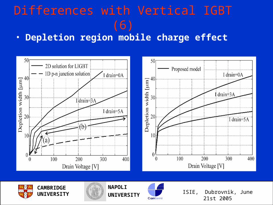
Differences with Vertical IGBT (6)
• Depletion region mobile charge effect

ISIE, Dubrovnik, June 21st 2005CAMBRIDGEUNIVERSITY
NAPOLI
UNIVERSITY
IGBT models not suited for LIGBT
• Voltage rise at turn-off is faster due to lower charge in the epilayer and slower depletion width expansion

ISIE, Dubrovnik, June 21st 2005CAMBRIDGEUNIVERSITY
NAPOLI
UNIVERSITY
Spice sub-circuit model for LIGBT
Currents and voltages Epilayer charge equation

ISIE, Dubrovnik, June 21st 2005CAMBRIDGEUNIVERSITY
NAPOLI
UNIVERSITY
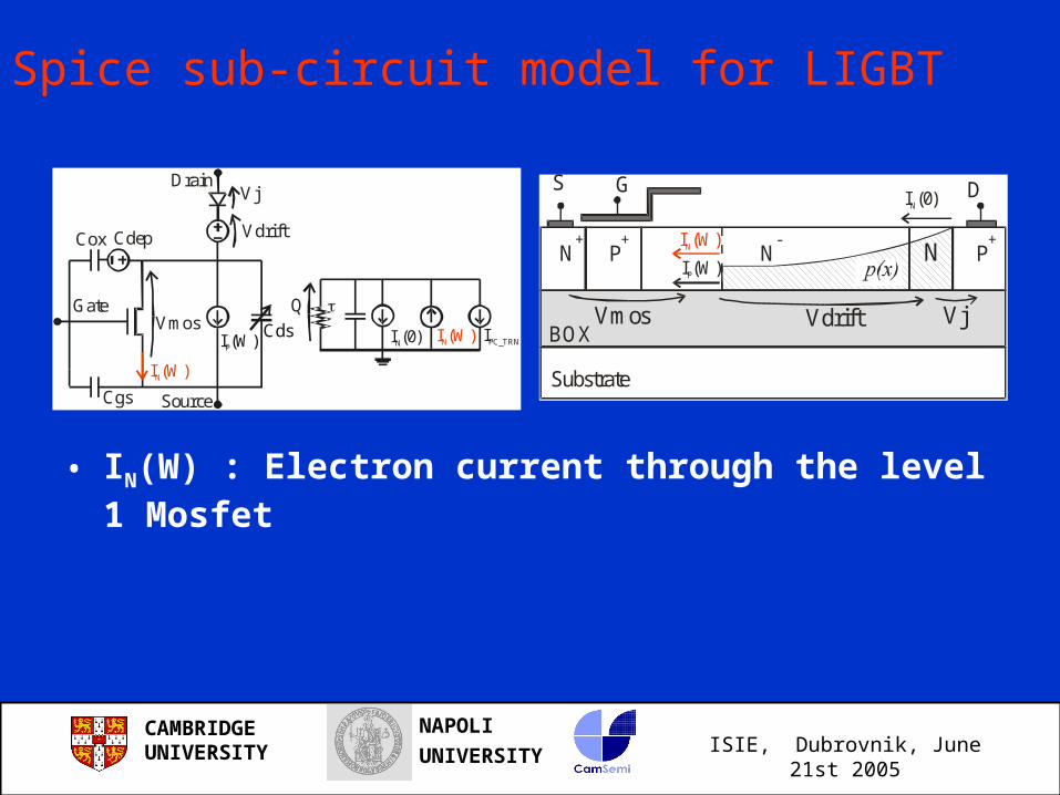
Spice sub-circuit model for LIGBT
Cox
Cgs
I (W)N
IPC_TRNI (0)NI (W)NI (W)P
Cdep
Cds
Q
Vdrift
Drain
Source
Gate
Vj
Vmos
N+
G DS
NN-
BOX
Substrate
P+
P+
I (0)N
VjVdriftVmos
I (W)N
I (W)P
• Vj : Emitter junction• Vdrift:Depends on the injected carriers
– analytic solution• Vmos: Mosfet (level 1)
ISIE, Dubrovnik, June 21st 2005CAMBRIDGEUNIVERSITY
NAPOLI
UNIVERSITY
Spice sub-circuit model for LIGBT
N+
G DS
NN-
BOX
Substrate
P+
P+
I (0)N
VjVdriftVmos
I (W)N
I (W)P
• IN(W) : Electron current through the level 1 Mosfet
Cox
Cgs
I (W)N
IPC_TRNI (0)NI (W)NI (W)P
Cdep
Cds
Q
Vdrift
Drain
Source
Gate
Vj
Vmos
ISIE, Dubrovnik, June 21st 2005CAMBRIDGEUNIVERSITY
NAPOLI
UNIVERSITY
Spice sub-circuit model for LIGBT
Cox
Cgs
I (W)N
IPC_TRNI (0)NI (W)NI (W)P
Cdep
Cds
Q
Vdrift
Drain
Source
Gate
Vj
Vmos
N+
G DS
NN-
BOX
Substrate
P+
P+
I (0)N
VjVdriftVmos
I (W)N
I (W)P
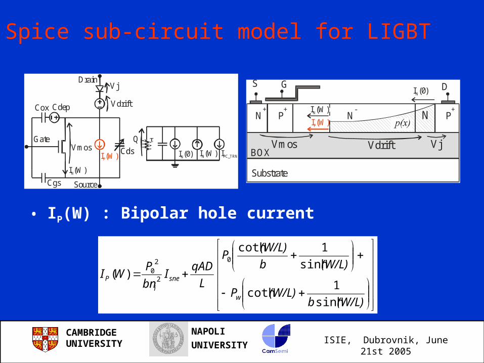
• IP(W) : Bipolar hole current
(W/L)b(W/L)P
(W/L)b
(W/L)P
L
qADI
bn
PWI
w
sne
i
P
sinh
1coth
sinh
1coth
)(0
2
20
ISIE, Dubrovnik, June 21st 2005CAMBRIDGEUNIVERSITY
NAPOLI
UNIVERSITY
Spice sub-circuit model for LIGBT
Cox
Cgs
I (W)N
IPC_TRNI (0)NI (W)NI (W)P
Cdep
Cds
Q
Vdrift
Drain
Source
Gate
Vj
Vmos
N+
G DS
NN-
BOX
Substrate
P+
P+
I (0)N
VjVdriftVmos
I (W)N
I (W)P
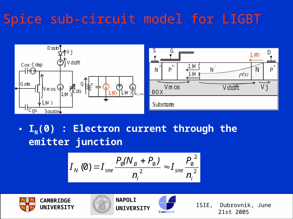
• IN(0) : Electron current through the emitter junction
2
20
200)0(
i
sne
i
BsneN
n
PI
n
)P(NPII

ISIE, Dubrovnik, June 21st 2005CAMBRIDGEUNIVERSITY
NAPOLI
UNIVERSITY
Spice sub-circuit model for LIGBT
Cox
Cgs
I (W)N
IPC_TRNI (0)NI (W)NI (W)P
Cdep
Cds
Q
Vdrift
Drain
Source
Gate
Vj
Vmos
• IPC_TRN : Transient current due to charge sweep-out
t
tWtWqApI TRNPC
_
Increasing Anode Voltage
Stable Anode Voltage
P
0
PW
Wt Wt+δt Wt+2δt
Time is increasing
0

ISIE, Dubrovnik, June 21st 2005CAMBRIDGEUNIVERSITY
NAPOLI
UNIVERSITY
Base charge equation
IN(W) is the MOSFET current
IN(0) is the emitter edge electron current
IPC_TRN is the charge sweep out current
The last term is for the recombination in the base
Q
IIWIt
QTRNPCNN
_0

ISIE, Dubrovnik, June 21st 2005CAMBRIDGEUNIVERSITY
NAPOLI
UNIVERSITY
Other model features
Carrier concentration dependent mobility model
Gate-Source Drain-Source and Gate-Drain capacitances are implemented
Physical based model with 17 parameters

ISIE, Dubrovnik, June 21st 2005CAMBRIDGEUNIVERSITY
NAPOLI
UNIVERSITY
Name Meaning Unit
Vth Threshold voltage V
Nb Drift doping cm^-3
Wb Drift region length (51e-4) cm
Wnw N well length cm
Wfp Field plate extension cm
un Electron mobility cm^2/Vs
up Hole mobility cm^2/Vs
A Device transversal area cm^2
Kp Mos transconductance A/V^2
Name Meaning Unit
Isne P+ emitter inverse saturation current
A
Cbcj Body Drift region depletion capacitance factor
F/cm^2
Cox oxide Gate Drain capacitance F/cm^2
Cgs gate source capacitance F/cm^2
Taub drift region ambipolar lifetime (0.35e-6)
s
pw_ratio P(0)/P(W)
W_inc Depletion width expansion factor
V_fp Field plate depletion voltage V
Spice circuit parameters

ISIE, Dubrovnik, June 21st 2005CAMBRIDGEUNIVERSITY
NAPOLI
UNIVERSITY
Proposed modelNumerical simulation
Ano
de c
urre
nt [A
]
Anode Voltage [V]0
0
Vg=5V
Vg=4V
Vg=3V
Vg=2V
1
1
2
2
3
3
4
4
5
5
Static characteristics
ISIE, Dubrovnik, June 21st 2005CAMBRIDGEUNIVERSITY
NAPOLI
UNIVERSITY
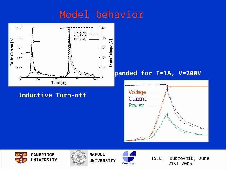
Model behavior
Inductive Turn-off
Expanded for I=1A, V=200V
VoltageCurrentPower
ISIE, Dubrovnik, June 21st 2005CAMBRIDGEUNIVERSITY
NAPOLI
UNIVERSITY
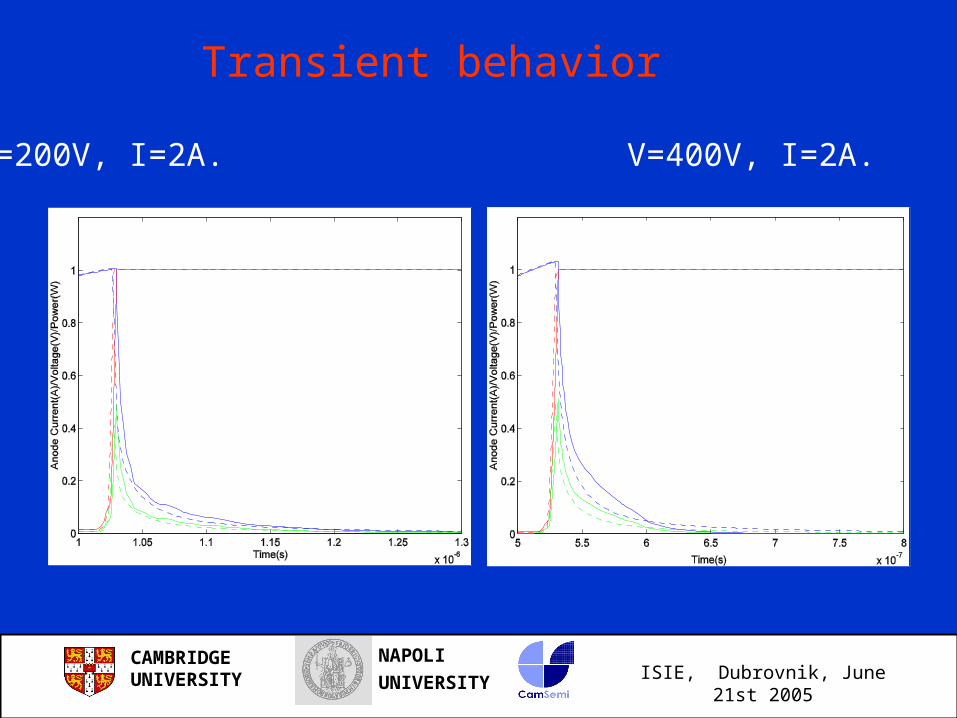
V=200V, I=2A. V=400V, I=2A.
Transient behavior
ISIE, Dubrovnik, June 21st 2005CAMBRIDGEUNIVERSITY
NAPOLI
UNIVERSITY
U 5
L I G B T
0
1
2A
NO
G A TE KA
T
V 12 0 0
0
V d d
G
0
A
R 1
1 0
R 4
2 0 0
0
V g t r
TD = 5 1 0 n
TF = 1 0 nP W = 5 0 0 nP E R = 1 0 0 0 n
V 1 = 5
TR = 1 0 n
V 2 = 0
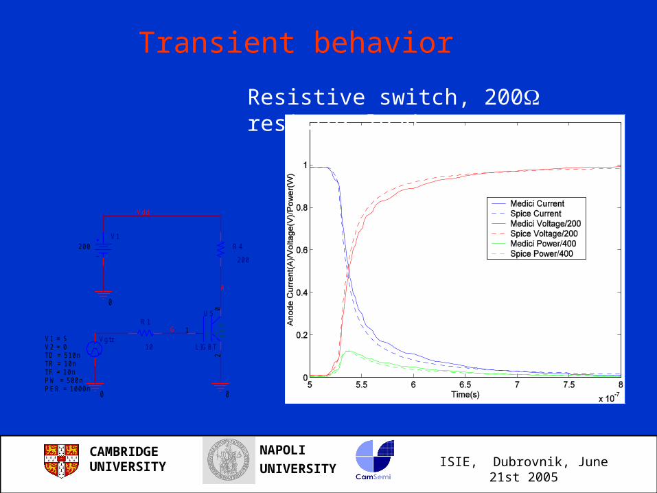
Resistive switch, 200 resistor load
Transient behavior

ISIE, Dubrovnik, June 21st 2005CAMBRIDGEUNIVERSITY
NAPOLI
UNIVERSITY
Model behavior
• Toff Energy vs. Von as a function of lifetime

ISIE, Dubrovnik, June 21st 2005CAMBRIDGEUNIVERSITY
NAPOLI
UNIVERSITY
Conclusion
• A physical based circuit model for Lateral IGBT• Implemented in Spice• Defined through 17 physical parameters• Compared against device numerical simulation• Extendable to Thick SOI and JI-LIGBT