camerachip ds 1.3 - adrirobot · ov528-b64 pin descriptions ... ov528-t64 pin assignment 7 figure...
TRANSCRIPT

CAMERACHIP™ DATASHEET
CameraChip™ Datasheet Datasheet – OV528 © OmniVision Technologies Inc., 2002
OVT OV528 Single Chip Camera-to-Serial Bridge
Last Modified: October 10, 2002 Document Version: 1.3
THIS DOCUMENT IS PROVIDED “AS IS” WITH NO WARRANTIES WHATSOEVER, INCLUDING ANY WARRANTY OF MERCHANTABILITY, NON-INFRINGEMENT, FITNESS FOR ANY PARTICULAR PURPOSE, OR ANY WARRANTY OTHERWISE ARISING OUT OF ANY PROPOSAL, SPECIFICATION OR SAMPLE. OmniVision Technologies Inc. disclaims all liability, including liability for infringement of any proprietary rights, relating to use of information in this document. No license, expressed or implied, by estoppels or otherwise, to any intellectual property rights is granted herein. *Third-party brands, names, and trademarks are the property of their respective owners.
Note: The information contained in this document is considered proprietary to OmniVision Technologies Inc. This information may be distributed only to individuals or organizations authorized by OmniVision Technologies, Inc. to receive said information. Individuals and/or organizations are not allowed to re-distribute said information without consent of OmniVision Technologies Inc. authorized representative(s).

DATASHEET
OV528 Datasheet Doc #DS201
© OmniVision Technologies Inc., 2002, version 1.0 Page 1
ContentsContents 1 Figures 2 Tables 3 Features 4
General Features .............................................................................................................................................................. 4 Camera Interfaces............................................................................................................................................................. 4 Serial Interfaces ................................................................................................................................................................ 4 The Compression Engine.................................................................................................................................................. 4 Miscellaneous ................................................................................................................................................................... 4 OV528-64 vs. OV528-100................................................................................................................................................. 4
Architecture 5 General Description .......................................................................................................................................................... 5 Functional Description....................................................................................................................................................... 5
Camera Sensors............................................................................................................................................................ 5 Program Memory........................................................................................................................................................... 5 OV528 Serial Bridge...................................................................................................................................................... 5
Pin Definitions 7 Pin Assignments ............................................................................................................................................................... 7 OV528-T64 Pin Descriptions............................................................................................................................................. 9 OV528-T100 Pin Descriptions......................................................................................................................................... 12 OV528-B64 Pin Descriptions .......................................................................................................................................... 16
Electrical Characteristics 19 Register Table & Command Set 20
Register Table................................................................................................................................................................. 20 Example of Command Set .............................................................................................................................................. 27
INITIAL (FFFFFF01h).................................................................................................................................................. 27 Preview Resolution for VGA Sensor............................................................................................................................ 28 DUMP (FFFFFF02h) ................................................................................................................................................... 29 SET REGISTER (FFFFFF03h).................................................................................................................................... 29 GET PICTURE (FFFFFF04h) ...................................................................................................................................... 29 SNAPSHOT (FFFFFF05h) .......................................................................................................................................... 29 SAVE DATA (FFFFFF06h).......................................................................................................................................... 29 RESET (FFFFFF08h) .................................................................................................................................................. 30 POWER OFF (FFFFFF09h) ........................................................................................................................................ 30 DATA (FFFFFF0Ah) .................................................................................................................................................... 30 GET REGISTER (FFFFFF0Bh) ................................................................................................................................... 30 DOWNLOAD PROGRAM (FFFFFF0Ch)..................................................................................................................... 30 SYNC (FFFFFF0Dh) ................................................................................................................................................... 31 ACK (FFFFFF0Eh) ...................................................................................................................................................... 31 NAK (FFFFFF0Fh) ...................................................................................................................................................... 31
Mechanical Information 32 OV528-T64 Package....................................................................................................................................................... 32 OV528-T100 Package..................................................................................................................................................... 33 OV528-B64 Package ...................................................................................................................................................... 34 Revision History .............................................................................................................................................................. 35

DATASHEET
OV528 Datasheet Doc #DS201
© OmniVision Technologies Inc., 2002, version 1.0 Page 2
Figures Figure 1. System Block Diagram 5 Figure 2. Functional Block Diagram 6 Figure 3. OV528-T64 Pin Assignment 7 Figure 4. OV528-T100 Pin Assignment 8 Figure 5. OV528-T64 Package 32 Figure 6. OV528-T100 Package 33 Figure 7. OV528-B64 Package 34

DATASHEET
OV528 Datasheet Doc #DS201
© OmniVision Technologies Inc., 2002, version 1.0 Page 3
Tables Table 1. OV528-64 vs. OV528-100 4 Table 2. OV528-T64 Pin Descriptions – All Pins in Numeric Order 9 Table 3. OV528-T64 Pin Descriptions – Camera Interface (12 pins) 10 Table 4. OV528-T64 Pin Descriptions – Serial Camera Control Bus (3 pins) 10 Table 5. OV528-T64 Pin Descriptions – Serial Interface (4 pins) 10 Table 6. OV528-T64 Pin Descriptions – Clock & Reset (7 pins) 11 Table 7. OV528-T64 Pin Descriptions – Serial Program ID (4 pins) 11 Table 8. OV528-T64 Pin Descriptions – GPIO (9 pins) 11 Table 9. OV528-T64 Pin Descriptions – Misc. (6 pins) 11 Table 10. OV528-T64 Pin Descriptions – Internal MC I/O Ports (1 pin) 11 Table 11. OV528-T64 Pin Descriptions – Power & Ground (18 pins) 11 Table 12. OV528-T100 Pin Descriptions – All Pins in Numeric Order 12 Table 13. OV528-T100 Pin Descriptions – Camera Interface (12 pins) 14 Table 14. OV528-T100 Pin Descriptions – Serial Camera Control Bus (3 pins) 14 Table 15. OV528-T100 Pin Descriptions – Serial Interface (4 pins) 14 Table 16. OV528-T100 Pin Descriptions – Clock & Reset (7 pins) 14 Table 17. OV528-T100 Pin Descriptions – Serial Program ID (7 pins) 14 Table 18. OV528-T100 Pin Descriptions – GPIO (15 pins) 15 Table 19. OV528-T100 Pin Descriptions – Misc. (7 pins) 15 Table 20. OV528-T100 Pin Descriptions –Internal MC I/O Ports (23 pins) 15 Table 21. OV528-T100 Pin Descriptions – Power & Ground (22 pins) 15 Table 22. OV528-B64 Pin Descriptions – All Pins in Numeric Order 16 Table 23. OV528-B64 Pin Descriptions – Camera Interface (12 pins) 17 Table 24. OV528-B64 Pin Descriptions – Serial Camera Control Bus (3 pins) 17 Table 25. OV528-B64 Pin Descriptions – Serial Interface (4 pins) 17 Table 26. OV528-B64 Pin Descriptions – Clock & Reset (7 pins) 18 Table 27. OV528-B64 Pin Descriptions – Serial Program ID (4 pins) 18 Table 28. OV528-B64 Pin Descriptions – GPIO (9 pins) 18 Table 29. OV528-B64 Pin Descriptions – Misc. (6 pins) 18 Table 30. OV528-B64 Pin Descriptions – Internal MC I/O Ports (2 pins) 18 Table 31. OV528-B64 Pin Descriptions – Power & Ground (18 pins) 18 Table 32. DC Electrical Characteristics 19 Table 33. Recommended Operating Conditions 19 Table 34. Register List 20 Table 35. Command List 27 Table 36. RS-232 Baud Rate 28

DATASHEET
OV528 Datasheet Doc #DS201
© OmniVision Technologies Inc., 2002, version 1.0 Page 4
Features General Features Low-cost, single-chip & low-powered solution for high resolution serial bus PDA/cellular phone camera accessory applications 3.3V I/O, 2.5V core, 64-pin/100-pin TQFP, 64-pin BGA No external DRAM required
Camera Interfaces OV76x0 VGA color digital cameras OV66x0 CIF color digital cameras 8-bit camera input interface Built-in down-sampling, clamping and windowing circuits for VGA/CIF/SIF/QCIF/160x128/80x64 image resolutions Built-in color conversion circuits for 4 gray/16 gray/256 gray/12-bit RGB/16-bit RGB/Pallet 256 RGB preview images
Serial Interfaces RS-232: 115.2K bps ~ 920K bps for transferring JPEG still pictures or 160x128 preview @8 bpp with 0.75~6 fps 4-wire serial bus: 1~2M bps for transferring JPEG still pictures or SIF (320x240) preview @4 bpp with 6~8 fps
The Compression Engine JPEG CODEC with variable quality settings for different resolutions
Miscellaneous Serial camera control bus General purpose I/O pins Built-in Micro Controller (MC) Built-in PLL
OV528-64 vs. OV528-100 Table 1. OV528-64 vs. OV528-100
OV528-64 OV528-100 Pin 64-pin 100-pin
Less MC Interface - Port: P2[0] - No Interrupt Pins - No Control Pins
More MC Interface - Port: P0[7:0], P2[7:0] - Interrupt: Int[1:0] - Control: WR_, RD_, ALE and PSEN_
Fewer IO VDD & VSS(Total 7-pairs) More IO VDD & VSS (Total 9-pairs) MC Pins
No Parallel I/F with program memory - No P_S
Parallel I/F with program memory - P_S
GPIO Pins Fewer GPIO(Total 8)
- GPIO0[1], GPIO0[3], GPIO0[7:6] - GPIO1[3:0]
More GPIO(Total 15) - GPIO0[7:1] - GPIO1[7:0]
Physical Difference
ID Pins Fewer ID pins (Total 4) - ID[3:0]
More ID pins(Total 7) - ID[6:0]
Program Memory Interface
- Cannot support parallel interface with program memory
- Cannot support optional program memory
- Supports parallel interface with program memory
- Supports optional program memory for large program size (up to 64k)
GPIO
- Total of 8 dedicated GPIO pins that can be used for general purpose I/O
- Total of 15 dedicated GPIO pins that can be used for general purpose I/O
- P0[7:0] and P2[7:0] can be used for general purpose
Functional Difference
Serial ID - Maximum 16 different IDs - Maximum 128 different IDs

DATASHEET
OV528 Datasheet Doc #DS201
© OmniVision Technologies Inc., 2002, version 1.0 Page 5
Architecture General Description The OV528 Serial Bus Camera System performs as a video camera or a JPEG compressed still camera and can be attached to a wireless or PDA host. When it performs as a video camera, the TFT-LCD panel of the host operates as a viewfinder. Users can send out a snapshot command from the host in order to capture a full resolution single-frame still picture. The picture is then compressed by the JPEG engine and transferred to the host.
Functional Description OV528, the Single Chip Camera-to-Serial Bridge, is a low-cost, single-chip & low-powered solution for high-resolution serial bus PDA/cellular phone camera accessory applications. Along with OV76x0/OV66x0 CMOS VGA/CIF color digital CameraChips, OV528 comprises a low-cost, highly integrated serial camera system. There is no additional DRAM required. The OV528 system, as shown in Figure 1, consists of a CameraChip, Program Memory and OV528 Serial Bridge.
Camera Sensors The OV528 supports OmniVision OV76x0/ and OV66x0 CameraChips with an 8-bit YCbCr interface.
Program Memory A program memory is required for the embedded MC to respond to host commands correctly, as well as to store all necessary parameters for adjusting image/compression qualities. A serial type program memory is required for OV528, while both serial and parallel types of program memory can be adapted to OV528-100. The contents of the program memory can be updated on the fly.
OV528 Serial Bridge The OV528 Serial Bridge is a controller chip that can transfer image data from CameraChips to wireless/PDA hosts. The OV528 takes 8-bit YCbCr 422 progressive video data from an OV76x0/OV66x0 CameraChip. The camera interface synchronizes with input video data and performs down-sampling, clamping and windowing functions with desired resolution, as well as color conversion that is requested by the user through serial bus host commands. The JPEG CODEC with variable quality settings can achieve higher compression ratio & better image quality for various image resolutions. The Serial Camera Control Bus is used to achieve greater flexibility in camera interface.
Figure 1. System Block Diagram
OV528SensorOV76x0OV66x0
(Optional)Program Memory
Host
EEPROM

DATASHEET
OV528 Datasheet Doc #DS201
© OmniVision Technologies Inc., 2002, version 1.0 Page 6
Figure 2. Functional Block Diagram
OV528SensorOV76x0OV66x0
CameraInterface JPEG
InterfaceMicroController
SerialInterface
(Optional)Program Memory
Host
EEPROM
Buffer
RS232
SerialInterfaceProgram
Buffer
Data Path
Control Path

DATASHEET
OV528 Datasheet Doc #DS201
© OmniVision Technologies Inc., 2002, version 1.0 Page 7
Pin Definitions Pin Assignments Figure 3. OV528-T64 Pin Assignment
49 Y0
35
IO_VDD4
36
GPIO06
38
DUMP_PRC
39
SEL_UART
40
CORE_VDD2
41
SCS_
42
CORE_VSS2
43
SIO1
44
SIO0
46
IO_VSS5
47
GPIO07
17 RTS_
20 CTS_
21 RXD
22 TXD
23 IO_VSS2
24 XIN
25 XOUT
26 IO_VDD3
27 ID0
29 SNAP_
30 TEST
31 IO_VSS3
2
PLL_SEL
3
CCLK
4
HREF
5
CORE_VSS1
6
VSYNC
7
CORE_VDD1
8
RESET_
10
IO_VDD1
11
SXOUT
12
SXIN
13
IO_VSS1
16
UCLK
58 Y4
59 Y5
60 IO_VDD6
61 Y6
62 Y7
64 PCLK
50 IO_VDD5
52 Y1
54 Y2
56 Y3
57 IO_VSS6
15
UCO_I
14
GPIO01
9
MCLK_SEL
18 IO_VDD2
32 GPIO03
28 EA_
19 P20
33
ID1
34
ID2
37
IO_VSS4
48
GPIO10
45
ID3
51 GPIO11
53 GPIO12
63 IO_VSS7
55 GPIO13
1
IO_VDD7
OV528-T64

DATASHEET
OV528 Datasheet Doc #DS201
© OmniVision Technologies Inc., 2002, version 1.0 Page 8
Figure 4. OV528-T100 Pin Assignment
76 Y0
51
WR_
52
INT0
53
ID1
54
ID2
55
IO_VDD6
56
ID4
57
GPIO06
58
INT1
59
IO_VSS6
60
DUMP_PRC
61
SEL_UART
62
CORE_VDD2
63
SCS_
64
CORE_VSS2
65
SIO0
66
RD_
67
IO_VDD7
68
SIO1
69
ID3
70
IO_VSS7
71
ID5
72
GPIO07
73
ALE
74
PSEN_
75
GPIO10
26 P0727 RTS_28 IO_VDD429 P2030 CTS_31 P2132 RXD33 P2234 P2335 TXD36 P2437 IO_VSS438 XIN39 XOUT40 IO_VDD541 P2542 ID043 EA_44 P2645 SNAP_46 P2747 TEST48 GPIO0249 IO_VSS550 GPIO3
1
P01
2
IO_VDD1
3
PLL_SEL
4
IO_VSS1
5
P02
6
CCLK
7
IO_VDD2
8
P03
9
HREF
10
IO_VSS2
11
P04
12
CORE_VSS1
13
VSYNC
14
CORE_VDD1
15
RESET_
16
P05
17
MCLK_SEL
18
IO_VDD3
19
SXOUT
20
SXIN
21
IO_VSS4
22
GPIO01
23
UCO_I
24
UCLK
25
P06
OV528-T10090 Y491 GPIO1592 Y593 IO_VDD994 Y695 GPIO1696 Y797 IO_VSS998 P0099 PCLK100 GPIO17
77 ID678 GPIO0479 IO_VDD880 GPIO1181 Y182 GPIO1283 Y284 GPIO1385 Y386 GPIO1487 GPIO0588 IO_VSS889 P_S

DATASHEET
OV528 Datasheet Doc #DS201
© OmniVision Technologies Inc., 2002, version 1.0 Page 9
OV528-T64 Pin Descriptions Table 2. OV528-T64 Pin Descriptions – All Pins in Numeric Order
Pin # Name I/O Function 1 DVDD Digital 3.3V power 2 PLL_SEL I PLL select 3 CCLK O Camera clock output 4 HREF I Camera horizontal window reference input 5 CVSS Digital ground 6 VSYNC I Camera vertical sync input 7 CVDD Digital 2.5V power 8 RESET_ I Power-on reset input. Low-active 9 MCLK_SEL I Master clock select. 1 from internal PLL. 0 from 48MHz crystal 10 DVDD Digital 3.3V power 11 SXOUT O Serial bus crystal output 12 SXIN I Serial bus crystal input 13 DVSS Digital ground 14 GPIO0[1] I/O General purpose I/O port 0 bit 1 15 UCO_I I External/internal MC select. 0 for internal MC. Must select internal MC for
OV528 16 UCLK O RS-232 master clock output 17 RTS_ I/O RS-232 RTS_ 18 DVDD Digital 3.3V power 19 P2[0] I/O Internal MC port 2 bit 0 20 CTS_ I RS-232 CTS_ 21 RXD I RS-232 RXD 22 TXD O RS-232 TXD 23 DVSS Digital ground 24 XIN I System crystal input 25 XOUT O System crystal output 26 DVDD Digital 3.3V power 27 ID[0] I/O Serial program memory ID bit 0 28 EA_ I/O Internal MC EA_ 29 SNAP_ I Snapshot button input. Low-active 30 TEST I Test mode enabled/disabled. 1 for enabled 31 DVSS Digital ground 32 GPIO0[3] I/O General purpose I/O port 0 bit 3 33 ID[1] I/O Serial program memory ID bit 1 34 ID[2] I/O Serial program memory ID bit 2 35 DVDD Digital 3.3V power 36 GPIO0[6] I/O General purpose I/O port 0 bit 6 37 DVSS Digital ground 38 DUMP_PRC I Host programming enabled/disabled. 1 for enabled 39 SEL_UART_ I Serial bus select. 0 for RS-232 40 CVDD Digital 2.5V power 41 SCS_ O Serial camera chip select output 42 CVSS Digital ground 43 SIO1 O Serial camera control signal 1

DATASHEET
OV528 Datasheet Doc #DS201
© OmniVision Technologies Inc., 2002, version 1.0 Page 10
Pin # Name I/O Function 44 SIO0 I/O Serial camera control signal 0 45 ID[3] I/O Serial program memory ID bit 3 46 DVSS Digital ground 47 GPIO0[7] I/O General purpose I/O port 0 bit 7 48 GPIO1[0] I/O General purpose I/O port 0 bit 0 49 Y[0] I Camera Y/Cb/Cr input bit 0 50 DVDD Digital 3.3V power 51 GPIO1[1] I/O General purpose I/O port 0 bit 1 52 Y[1] I Camera Y/Cb/Cr input bit 0 53 GPIO1[2] I/O General purpose I/O port 0 bit 2 54 Y[2] I Camera Y/Cb/Cr input bit 0 55 GPIO1[3] I/O General purpose I/O port 0 bit 3 56 Y[3] I Camera Y/Cb/Cr input bit 0 57 DVSS Digital ground 58 Y[4] I Camera Y/Cb/Cr input bit 0 59 Y[5] I Camera Y/Cb/Cr input bit 0 60 DVDD Digital 3.3V power 61 Y[6] I Camera Y/Cb/Cr input bit 0 62 Y[7] I Camera Y/Cb/Cr input bit 0 63 DVSS Digital ground 64 PCLK I Camera pixel clock input Table 3. OV528-T64 Pin Descriptions – Camera Interface (12 pins)
Pin # Name I/O Function 3 CCLK O Camera clock output 4 HREF I Camera horizontal window reference input 6 VSYNC I Camera vertical sync input 49, 52, 54, 56, 58, 59, 61, 62
Y[0:7] I Camera Y/Cb/Cr inputs
64 PCLK I Camera pixel clock input Table 4. OV528-T64 Pin Descriptions – Serial Camera Control Bus (3 pins)
Pin # Name I/O Function 41 SCS_ O Serial camera chip select output 43 SIO1 O Serial camera control signal 1 44 SIO0 I/O Serial camera control signal 0
Table 5. OV528-T64 Pin Descriptions – Serial Interface (4 pins)
Pin # Name I/O Function 17 RTS_ I/O RS-232 RTS_ 20 CTS_ I RS-232 CTS_ 21 RXD I RS-232 RXD 22 TXD O RS-232 TXD

DATASHEET
OV528 Datasheet Doc #DS201
© OmniVision Technologies Inc., 2002, version 1.0 Page 11
Table 6. OV528-T64 Pin Descriptions – Clock & Reset (7 pins) Pin # Name I/O Function
2 PLL_SEL I PLL select 8 RESET_ I Power-on reset input. Low-active 11 SXOUT O Serial bus crystal output 12 SXIN I Serial bus crystal input 16 UCLK O RS-232 master clock output 24 XIN I System crystal input 25 XOUT O System crystal output
Table 7. OV528-T64 Pin Descriptions – Serial Program ID (4 pins)
Pin # Name I/O Function 27, 33, 34, 45 ID[0:3] I/O Serial program memory ID bit 0~3
Table 8. OV528-T64 Pin Descriptions – GPIO (9 pins)
Pin # Name I/O Function 14 GPIO0[1] I/O General purpose I/O port 0 bit 1 32 GPIO0[3] I/O General purpose I/O port 0 bit 3 36, 47 GPIO0[6:7] I/O General purpose I/O port 0 bit 6~7 48, 51, 53, 55 GPIO1[0:3] I/O General purpose I/O port 0 bit 0~3
Table 9. OV528-T64 Pin Descriptions – Misc. (6 pins)
Pin # Name I/O Function 9 MCLK_SEL I Master clock select. 1 from internal PLL. 0 from 48MHz crystal 15 UCO_I I External/internal MC select. 0 for internal MC. Must select internal MC for
OV528 29 SNAP_ I Snapshot button input. Low-active 30 TEST I Test mode enabled/disabled. 1 for enabled 38 DUMP_PRC I Host programming enabled/disabled. 1 for enabled 39 SEL_UART_ I Serial bus select. 0 for RS-232
Table 10. OV528-T64 Pin Descriptions – Internal MC I/O Ports (1 pin)
Pin # Name I/O Function 19 P2[0] I/O Internal MC port 2 bit 0 28 EA_ I/O Internal MC EA_
Table 11. OV528-T64 Pin Descriptions – Power & Ground (18 pins)
Pin # Name I/O Function 1, 10, 18, 26, 35, 50, 60
DVDD Digital 3.3V power
7, 40 CVDD Digital 2.5V power 13, 23, 31, 37, 46, 57, 63
DVSS Digital ground
5, 42 CVSS Digital ground

DATASHEET
OV528 Datasheet Doc #DS201
© OmniVision Technologies Inc., 2002, version 1.0 Page 12
OV528-T100 Pin Descriptions Table 12. OV528-T100 Pin Descriptions – All Pins in Numeric Order
Pin # Name I/O Function 1 P0[1] I/O Internal MC port 0 bit 1 2 DVDD Digital 3.3V power 3 PLL_SEL I PLL select 4 DVSS Digital ground 5 P0[2] I/O Internal MC port 0 bit 2 6 CCLK O Camera clock output 7 DVDD Digital 3.3V power 8 P0[3] I/O Internal MC port 0 bit 3 9 HREF I Camera horizontal window reference input 10 DVSS Digital ground 11 P0[4] I/O Internal MC port 0 bit 4 12 CVSS Digital ground 13 VSYNC I Camera vertical sync input 14 CVDD Digital 2.5V power 15 RESET_ I Power-on reset input. Low-active 16 P0[5] I/O Internal MC port 0 bit 5 17 MCLK_SEL I Master clock select. 1 from internal PLL. 0 from 48MHz crystal 18 DVDD Digital 3.3V power 19 SXOUT O Serial bus crystal output 20 SXIN I Serial bus crystal input 21 DVSS Digital ground 22 GPIO0[1] I/O General purpose I/O port 0 bit 1 23 UCO_I I External/internal MC select. 0 for internal MC 24 UCLK O RS-232 master clock output 25 P0[6] I/O Internal MC port 0 bit 6 26 P0[7] I/O Internal MC port 0 bit 7 27 RTS_ I/O RS-232 RTS_ 28 DVDD Digital 3.3V power 29 P2[0] I/O Internal MC port 2 bit 0 30 CTS_ I RS-232 CTS_ 31 P2[1] I/O Internal MC port 2 bit 1 32 RXD I RS-232 RXD 33 P2[2] I/O Internal MC port 2 bit 2 34 P2[3] I/O Internal MC port 2 bit 3 35 TXD O RS-232 TXD 36 P2[4] I/O Internal MC port 2 bit 4 37 DVSS Digital ground 38 XIN I System crystal input 39 XOUT O System crystal output 40 DVDD Digital 3.3V power 41 P2[5] I/O Internal MC port 2 bit 5 42 ID[0] I/O Serial program memory ID bit 0 43 EA_ I Internal MC EA_ 44 P2[6] I/O Internal MC port 2 bit 6

DATASHEET
OV528 Datasheet Doc #DS201
© OmniVision Technologies Inc., 2002, version 1.0 Page 13
Pin # Name I/O Function 45 SNAP_ I Snapshot button input. Low-active 46 P2[7] I/O Internal MC port 2 bit 7 47 TEST I Test mode enabled/disabled. 1 for enabled 48 GPIO0[2] I/O General purpose I/O port 0 bit 2 49 DVSS Digital ground 50 GPIO0[3] I/O General purpose I/O port 0 bit 3 51 WR_ I/O Internal MC WR_ 52 INT0_ O Internal MC INT0_ 53 ID[1] I/O Serial program memory ID bit 1 54 ID[2] I/O Serial program memory ID bit 2 55 DVDD Digital 3.3V power 56 ID[4] I/O Serial program memory ID bit 4 57 GPIO0[6] I/O General purpose I/O port 0 bit 6 58 INT1_ O Internal MC INT1_ 59 DVSS Digital ground 60 DUMP_PRC I Host programming enabled/disabled. 1 for enabled 61 SEL_UART_ I Serial bus select. 0 for RS-232 62 CVDD Digital 2.5V power 63 SCS_ O Serial camera chip select output 64 CVSS Digital ground 65 SIO1 O Serial camera control signal 1 66 RD_ I/O Internal MC RD_ 67 DVDD Digital 3.3V power 68 SIO0 I/O Serial camera control signal 0 69 ID[3] I/O Serial program memory ID bit 3 70 DVSS Digital ground 71 ID[5] I/O Serial program memory ID bit 5 72 GPIO0[7] I/O General purpose I/O port 0 bit 7 73 ALE I/O Internal MC ALE 74 PSEN_ O Internal MC PSEN_ 75 GPIO1[0] I/O General purpose I/O port 0 bit 0 76 Y[0] I Camera Y/Cb/Cr input bit 0 77 ID[6] I/O Serial program memory ID bit 6 78 GPIO0[4] I/O General purpose I/O port 0 bit 4 79 DVDD Digital 3.3V power 80 GPIO1[1] I/O General purpose I/O port 0 bit 1 81 Y[1] I Camera Y/Cb/Cr input bit 1 82 GPIO1[2] I/O General purpose I/O port 0 bit 2 83 Y[2] I Camera Y/Cb/Cr input bit 2 84 GPIO1[3] I/O General purpose I/O port 0 bit 3 85 Y[3] I Camera Y/Cb/Cr input bit 3 86 GPIO1[4] I/O General purpose I/O port 0 bit 4 87 GPIO0[5] I/O General purpose I/O port 0 bit 5 88 DVSS Digital ground 89 P_S I Serial/parallel program memory select. 1 for parallel. 0 for serial 90 Y[4] I Camera Y/Cb/Cr input bit 4 91 GPIO1[5] I/O General purpose I/O port 0 bit 5

DATASHEET
OV528 Datasheet Doc #DS201
© OmniVision Technologies Inc., 2002, version 1.0 Page 14
Pin # Name I/O Function 92 Y[5] I Camera Y/Cb/Cr input bit 5 93 DVDD Digital 3.3V power 94 Y[6] I Camera Y/Cb/Cr input bit 6 95 GPIO1[6] I/O General purpose I/O port 0 bit 6 96 Y[7] I Camera Y/Cb/Cr input bit 7 97 DVSS Digital ground 98 P0[0] I/O Internal MC port 0 bit 0 99 PCLK I Camera pixel clock input 100 GPIO1[7] I/O General purpose I/O port 0 bit 7 Table 13. OV528-T100 Pin Descriptions – Camera Interface (12 pins)
Pin # Name I/O Function 6 CCLK O Camera clock output 9 HREF I Camera horizontal window reference input 13 VSYNC I Camera vertical sync input 76, 81, 83, 85, 90, 92, 94, 96
Y[0:7] I Camera Y/Cb/Cr inputs
99 PCLK I Camera pixel clock input Table 14. OV528-T100 Pin Descriptions – Serial Camera Control Bus (3 pins)
Pin # Name I/O Function 63 SCS_ O Serial camera chip select output 65 SIO1 O Serial camera control signal 1 68 SIO0 I/O Serial camera control signal 0
Table 15. OV528-T100 Pin Descriptions – Serial Interface (4 pins)
Pin # Name I/O Function 27 RTS_ I/O RS-232 RTS_ 30 CTS_ I RS-232 CTS_ 32 RXD I RS-232 RXD 35 TXD O RS-232 TXD
Table 16. OV528-T100 Pin Descriptions – Clock & Reset (7 pins)
Pin # Name I/O Function 3 PLL_SEL I PLL select 15 RESET_ I Power-on reset input. Low-active 19 SXOUT O Serial bus crystal output 20 SXIN I Serial bus crystal input 24 UCLK O RS-232 master clock output 38 XIN I System crystal input 39 XOUT O System crystal output
Table 17. OV528-T100 Pin Descriptions – Serial Program ID (7 pins)
Pin # Name I/O Function 42, 53, 54, 69, 56, 71, 77
ID[0:6] I/O Serial program memory ID bit 0~6

DATASHEET
OV528 Datasheet Doc #DS201
© OmniVision Technologies Inc., 2002, version 1.0 Page 15
Table 18. OV528-T100 Pin Descriptions – GPIO (15 pins) Pin # Name I/O Function
22, 48, 50, 78, 87, 57, 72
GPIO0[1:7] I/O General purpose I/O port 0 bit 1~7
75, 80, 82, 84, 86, 91, 95, 100
GPIO1[0:7] I/O General purpose I/O port 0 bit 0~7
Table 19. OV528-T100 Pin Descriptions – Misc. (7 pins)
Pin # Name I/O Function 17 MCLK_SEL I Master clock select. 1 from internal PLL. 0 from 48MHz crystal 23 UCO_I I External/internal MC select. 0 for internal MC 45 SNAP_ I Snapshot button input. Low-active 47 TEST I Test mode enabled/disabled. 1 for enabled 60 DUMP_PRC I Host programming enabled/disabled. 1 for enabled 61 SEL_UART_ I Serial bus select. 0 for RS-232 89 P_S I Serial/parallel program memory select. 1 for parallel. 0 for serial
Table 20. OV528-T100 Pin Descriptions –Internal MC I/O Ports (23 pins)
Pin # Name I/O Function 98, 1, 5, 8, 11, 16, 25, 26
P0[0:7] I/O Internal MC port 0 bit 0~7
29, 31, 33, 34, 36, 41, 44, 46
P2[0:7] I/O Internal MC port 2 bit 0~7
43 EA_ I Internal MC EA_ 51 WR_ I/O Internal MC WR_ 52 INT0_ O Internal MC INT0_ 58 INT1_ O Internal MC INT1_ 66 RD_ I/O Internal MC RD_ 73 ALE I/O Internal MC ALE 74 PSEN_ O Internal MC PSEN_
Table 21. OV528-T100 Pin Descriptions – Power & Ground (22 pins)
Pin # Name I/O Function 2, 7, 18, 28, 40, 55, 67, 79, 93
DVDD Digital 3.3V power
14, 62 CVDD Digital 2.5V power 4, 10, 21, 37, 49, 59, 70, 88, 97
DVSS Digital ground
12, 64 CVSS Digital ground

DATASHEET
OV528 Datasheet Doc #DS201
© OmniVision Technologies Inc., 2002, version 1.0 Page 16
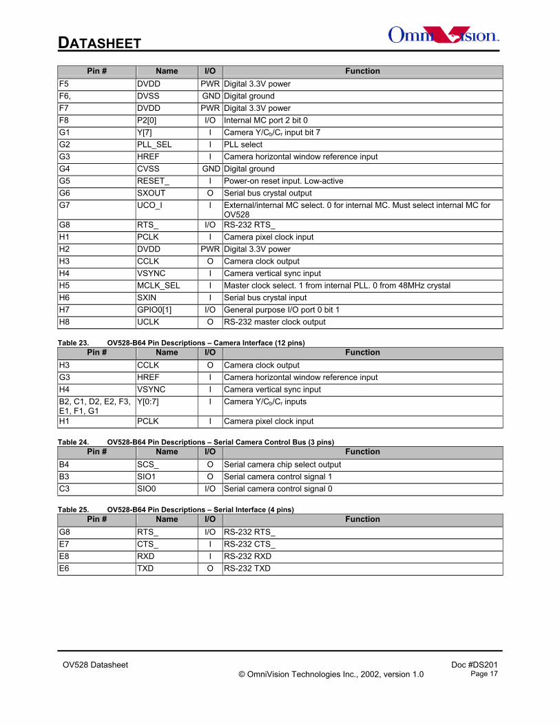
OV528-B64 Pin Descriptions Table 22. OV528-B64 Pin Descriptions – All Pins in Numeric Order
Pin # Name I/O Function A1 GPIO1[0] I/O General purpose I/O port 0 bit 0 A2 GPIO0[7] I/O General purpose I/O port 0 bit 7 A3 ID[3] I/O Serial program memory ID bit 3 A4 CVSS GND Digital ground A5 DUMP_PRC I Host programming enabled/disabled. 1 for enabled A6 DVDD PWR Digital 3.3V power A7 ID[1] I/O Serial program memory ID bit 1 A8 GPIO0[3] I/O General purpose I/O port 0 bit 3 B1 DVDD PWR Digital 3.3V power B2 Y[0] I Camera Y/Cb/Cr input bit 0 B3 SIO1 O Serial camera control signal 1 B4 SCS_ O Serial camera chip select output B5 SEL_UART_ I Serial bus select. 0 for RS-232 B6 GPIO0[6] I/O General purpose I/O port 0 bit 6 B7 ID[2] I/O Serial program memory ID bit 2 B8 TEST I Test mode enabled/disabled. 1 for enabled C1 Y[1] I Camera Y/Cb/Cr input bit 1 C2 GPIO1[1] I/O General purpose I/O port 0 bit 1 C3 SIO0 I/O Serial camera control signal 0 C4 CVDD PWR Digital 2.5V power C5 DVSS GND Digital ground C6 ID[0] I/O Serial program memory ID bit 0 C7 EA_ I/O Internal MC EA_ C8 SNAP_ I Snapshot button input. Low-active D1 GPIO1[3] I/O General purpose I/O port 0 bit 3 D2 Y[2] I Camera Y/Cb/Cr input bit 2 D3 GPIO1[2] I/O General purpose I/O port 0 bit 2 D4 DVSS GND Digital ground D5 DVSS GND Digital ground D6 XIN I System crystal input D7 XOUT O System crystal output D8 DVDD PWR Digital 3.3V power E1 Y[5] I Camera Y/Cb/Cr input bit 3 E2 Y[3] I Camera Y/Cb/Cr input bit 4 E3 DVSS GND Digital ground E4 DVSS GND Digital ground E5 DVSS GND Digital ground E6 TXD O RS-232 TXD E7 CTS_ I RS-232 CTS_ E8 RXD I RS-232 RXD F1 Y[6] I Camera Y/Cb/Cr input bit 6 F2 DVDD PWR Digital 3.3V power F3 Y[4] I Camera Y/Cb/Cr input bit 4 F4 CVDD PWR Digital 2.5V power
DATASHEET
OV528 Datasheet Doc #DS201
© OmniVision Technologies Inc., 2002, version 1.0 Page 17
Pin # Name I/O Function F5 DVDD PWR Digital 3.3V power F6, DVSS GND Digital ground F7 DVDD PWR Digital 3.3V power F8 P2[0] I/O Internal MC port 2 bit 0 G1 Y[7] I Camera Y/Cb/Cr input bit 7 G2 PLL_SEL I PLL select G3 HREF I Camera horizontal window reference input G4 CVSS GND Digital ground G5 RESET_ I Power-on reset input. Low-active G6 SXOUT O Serial bus crystal output G7 UCO_I I External/internal MC select. 0 for internal MC. Must select internal MC for
OV528 G8 RTS_ I/O RS-232 RTS_ H1 PCLK I Camera pixel clock input H2 DVDD PWR Digital 3.3V power H3 CCLK O Camera clock output H4 VSYNC I Camera vertical sync input H5 MCLK_SEL I Master clock select. 1 from internal PLL. 0 from 48MHz crystal H6 SXIN I Serial bus crystal input H7 GPIO0[1] I/O General purpose I/O port 0 bit 1 H8 UCLK O RS-232 master clock output Table 23. OV528-B64 Pin Descriptions – Camera Interface (12 pins)
Pin # Name I/O Function H3 CCLK O Camera clock output G3 HREF I Camera horizontal window reference input H4 VSYNC I Camera vertical sync input B2, C1, D2, E2, F3, E1, F1, G1
Y[0:7] I Camera Y/Cb/Cr inputs
H1 PCLK I Camera pixel clock input Table 24. OV528-B64 Pin Descriptions – Serial Camera Control Bus (3 pins)
Pin # Name I/O Function B4 SCS_ O Serial camera chip select output B3 SIO1 O Serial camera control signal 1 C3 SIO0 I/O Serial camera control signal 0
Table 25. OV528-B64 Pin Descriptions – Serial Interface (4 pins)
Pin # Name I/O Function G8 RTS_ I/O RS-232 RTS_ E7 CTS_ I RS-232 CTS_ E8 RXD I RS-232 RXD E6 TXD O RS-232 TXD
DATASHEET
OV528 Datasheet Doc #DS201
© OmniVision Technologies Inc., 2002, version 1.0 Page 18
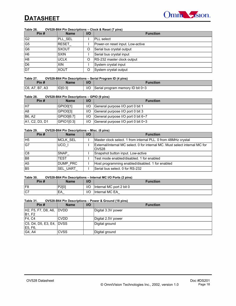
Table 26. OV528-B64 Pin Descriptions – Clock & Reset (7 pins) Pin # Name I/O Function
G2 PLL_SEL I PLL select G5 RESET_ I Power-on reset input. Low-active G6 SXOUT O Serial bus crystal output H6 SXIN I Serial bus crystal input H8 UCLK O RS-232 master clock output D6 XIN I System crystal input D7 XOUT O System crystal output
Table 27. OV528-B64 Pin Descriptions – Serial Program ID (4 pins)
Pin # Name I/O Function C6, A7, B7, A3 ID[0:3] I/O Serial program memory ID bit 0~3
Table 28. OV528-B64 Pin Descriptions – GPIO (9 pins)
Pin # Name I/O Function H7 GPIO0[1] I/O General purpose I/O port 0 bit 1 A8 GPIO0[3] I/O General purpose I/O port 0 bit 3 B6, A2 GPIO0[6:7] I/O General purpose I/O port 0 bit 6~7 A1, C2, D3, D1 GPIO1[0:3] I/O General purpose I/O port 0 bit 0~3
Table 29. OV528-B64 Pin Descriptions – Misc. (6 pins)
Pin # Name I/O Function H5 MCLK_SEL I Master clock select. 1 from internal PLL. 0 from 48MHz crystal G7 UCO_I I External/internal MC select. 0 for internal MC. Must select internal MC for
OV528 C8 SNAP_ I Snapshot button input. Low-active B8 TEST I Test mode enabled/disabled. 1 for enabled A5 DUMP_PRC I Host programming enabled/disabled. 1 for enabled B5 SEL_UART_ I Serial bus select. 0 for RS-232
Table 30. OV528-B64 Pin Descriptions – Internal MC I/O Ports (2 pins)
Pin # Name I/O Function F8 P2[0] I/O Internal MC port 2 bit 0 C7 EA_ I/O Internal MC EA_
Table 31. OV528-B64 Pin Descriptions – Power & Ground (18 pins)
Pin # Name I/O Function H2, F5, F7, D8, A6, B1, F2
DVDD Digital 3.3V power
F4, C4 CVDD Digital 2.5V power C5, D4, D5, E3, E4, E5, F6,
DVSS Digital ground
G4, A4 CVSS Digital ground

DATASHEET
OV528 Datasheet Doc #DS201
© OmniVision Technologies Inc., 2002, version 1.0 Page 19
Electrical Characteristics Table 32. DC Electrical Characteristics VDD = 3.3V+10%, TA = 0 to 125oC
Symbol Parameter Condition Min Typ Max Unit VIH High level input voltage CMOS 0.7xVDD V VIH High level input voltage TTL 2.0 V VIL Low level input voltage CMOS 0.3xVDD V VIL Low level input voltage TTL 0.8 V VOH High level output voltage 2.4 VDD V VOL Low level output voltage 0.2 0.4 V Is Suspend Current Suspend 90 uA Io Normal Operation Current Operating 55 mA
Table 33. Recommended Operating Conditions
Symbol Parameter Rating Unit VDD DC supply voltage 3.3V (I/O) 3.0 to 3.6 V VCC DC supply voltage 2.5V (core) 2.25 to 2.75 V TA Commercial temperature 0 to 125 oC

DATASHEET
OV528 Datasheet Doc #DS201
© OmniVision Technologies Inc., 2002, version 1.0 Page 20
Register Table & Command Set Register Table Table 34. Register List
Register Address
Register Name
R/W Function Default Value
00h CID RW Chip ID Default ID is for OV528. Users can use this register for sensor ID.
28h
01h HSB RW Horizontal start byte of image windowing 01h 02h VSB RW Vertical start byte of image windowing 01h 03h HPL RW Horizontal pixel length. The pixel length = HPL*4. The default
horizontal pixel length is 640 A0h
04h VPL RW Vertical pixel length. The pixel length = VPL*4. The default vertical pixel length is 480
78h
05h PLC RW Polarity control Bit 7~3: Reserved Bit 2: PCLK Bit 1: HREF Bit 0: VSYNC 0: inverted 1: normal
03h
06h IDC RW Bit 7: Enable Bit 6~0: Image disable counter. After sensor starting, users can decide how many frames to discard before capturing.
81h
07h RSVD RW Reserved 00h 08h JPC RW JPEG control
Bit 7: global JPEG enable Bit 6: JPEG decoder enable Bit 5~1: JPEG control setting Bit 0: JPEG encoder enable Please use only those value below 00h: update quantization table 9Fh: encoding BEh: stop encoding C2h: decoding 82h: stop decoding
00h
09h PVC RW Preview control Bit 7: Snapshot button status. Read only 3Fh: start 00h: stop
00h
0Ah HBB RW Buffer transfer size – high byte (Real_Size/2) 28h 0Bh LBB RW Buffer transfer size – low byte (Real_Size/2) 15h

DATASHEET
OV528 Datasheet Doc #DS201
© OmniVision Technologies Inc., 2002, version 1.0 Page 21
Register Address
Register Name
R/W Function Default Value
0Ch SBC RW Serial bus control Bit 7: RTS_ polarity control 0: inverted 1: normal Bit 6: Phase control Bit 5: Bit ordering 0: low bit first 1: high bit first Bit 4: TXD/RXD polarity control 0: inverted 1: normal Bit 3: MC program control 0: normal 1: download via serial bus Bit 2~0: serial bus control enabled/disabled 7h: enabled others: disabled
1Fh
0Dh UBR RW RS-232 baud rate control Baud rate = SXIN / 2 / (UBR+1)
7Fh
0Eh UDIV RW UCLK divider 80h: UCLK = XIN others: UCLK = XIN / 2 / (UDIV+1)
01h
0Fh CDIV RW CCLK divider 80h: CCLK = XIN others: CCLK = XIN*2 / (CDIV+1)
01h
10h CCC RW Color conversion control Bit 7: Reserved Bit 6~5: Down-sampling 0: normal 1: %2 2: %4 3: %8 Bit 4: Gray/Color select 0: gray 1: color Bit 3~2: Color select 0: 8-bit color 1: 12-bit color 2: 16-bit color 3: reserved Bit 1~0: Gray select 0: 4 gray 1: 16 gray 2: 256 gray 3: reserved
00h

DATASHEET
OV528 Datasheet Doc #DS201
© OmniVision Technologies Inc., 2002, version 1.0 Page 22
Register Address
Register Name
R/W Function Default Value
11h BFC RW Buffer control Bit 7: Reserved Bit 6: Write buffer failure table 0: enabled 1: disabled Bit 5~3: Buffer access mode 0: JPEG encoder access 3: MC access 4: JPEG decoder access others: forbidden Bit 2: Buffer failure table 0: disabled 1: enabled Bit 1: Address auto increment 0: disabled 1: enabled Bit 0: Write/read buffer 0: write 1: read
00h
12h BWA RW Buffer failure table write address 00h 13h HBWA RW High byte address for MC to access buffer 00h 14h LBWA RW Low byte address for MC to access buffer 00h 15h HBWD RW Highest byte of write data for buffer failure table 00h 16h MBWD RW Middle byte of write data for buffer failure table 00h 17h LBWD RW Lowest byte of write data for buffer failure table 00h 18h HBRD R Highest byte of read data for buffer failure table ~ 19h MBRD R Middle byte of read data for buffer failure table ~ 1Ah LBRD R Lowest byte of read data for buffer failure table ~ 1Bh BAC RW Buffer access control
0: MC access 1: JPEG encoder access 2: JPEG decoder access others: forbidden
01h
1Ch HBJPB RW High byte address of JPEG buffer for MC access 00h 1Dh LBJPB RW Low byte address of JPEG buffer for MC access 00h 1Eh HBJPWD RW High byte write data of JPEG buffer for MC access 00h 1Fh LBJPWD RW Low byte write data of JPEG buffer for MC access 00h 20h HBJPRD R High byte read data of JPEG buffer for MC access ~ 21h LBJPWD R Low byte read data of JPEG buffer for MC access ~ 22h HBBWD RW High byte write data of buffer for MC access 00h 23h LBBWD RW Low byte write data of buffer for MC access 00h 24h HBBRD R High byte read data of buffer for MC access ~ 25h LBBRD R Low byte read data of buffer for MC access ~ 26H HBSRD R High byte read data of serial bus for MC access ~ 27h LBSRD R Low byte read data of serial bus for MC access ~

DATASHEET
OV528 Datasheet Doc #DS201
© OmniVision Technologies Inc., 2002, version 1.0 Page 23
Register Address
Register Name
R/W Function Default Value
28h CHC RW Chip control Bit 7~6: Reserved Bit 5: JPEG decoding 0: disabled 1: enabled Bit 4: Serial bus IN control 0: Read MC commands from the host 1: Read data from the host to buffer Bit 3~2: Serial bus OUT control 0: Write preview image to the host 1: Write JPEG still picture to the host 2: Write MC commands to the host Bit 1~0: JPEG encoding/Buffer transfer 0: Transfer data from the host to buffer 3: JPEG encoding
00h
29h HBSWD RW High byte write data of serial bus for MC access 00h 2Ah LBSWD RW Low byte write data of serial bus for MC access 00h 2Bh CSD R Current data byte received from serial bus ~ 2Ch RSTC W Reset control
Bit 2: Logic reset 0: reset 1: normal Bit 1: System reset 0: reset 1: normal Bit 0: Suspend 0: normal 1: suspend
06h
2Dh RUST RW Resume start time 00h 2Eh RUET RW Resume end time 00h 2Fh
~ 47h
RSVD ~ Reserved ~
48h C0 RW R matrix Y coefficient. R=C0*Y+C1* Cr+C2* Cb+ROF 40h 49h C1 RW R matrix Cr coefficient 00h 4Ah C2 RW R matrix Cb coefficient 58h 4Bh ROF RW R matrix offset 00h 4Ch C3 RW G matrix Y coefficient. G=C3*Y+C4* Cr+C5* Cb+GOF 40h 4Dh C4 RW G matrix Cr coefficient 96h 4Eh C5 RW G matrix Cb coefficient Adh 4Fh GOF RW G matrix offset 00h 50h C6 RW B matrix Y coefficient. B=C6*Y+C7* Cr+C8* Cb+BOF 40h 51h C7 RW B matrix Cr coefficient 6Fh 52h C8 RW B matrix Cb coefficient 00h 53h BOF RW B matrix offset 00h 54h RSTP0 RW R step conversion 0 24h 55h RSTP1 RW R step conversion 1 49h 56h RSTP2 RW R step conversion 2 6Dh 57h RSTP3 RW R step conversion 3 92h 58h RSTP4 RW R step conversion 4 B6h 59h RSTP5 RW R step conversion 5 DBh 5Ah RSTP6 RW R step conversion 6 FFh 5Bh GSTP0 RW G step conversion 0 24h 5Ch GSTP1 RW G step conversion 1 49h 5Dh GSTP2 RW G step conversion 2 6Dh 5Eh GSTP3 RW G step conversion 3 92h 5Fh GSTP4 RW G step conversion 4 B6h

DATASHEET
OV528 Datasheet Doc #DS201
© OmniVision Technologies Inc., 2002, version 1.0 Page 24
Register Address
Register Name
R/W Function Default Value
60h GSTP5 RW G step conversion 5 DBh 61h GSTP6 RW G step conversion 6 FFh 62h BSTP0 RW B step conversion 0 55h 63h BSTP1 RW B step conversion 1 AAh 64h BSTP2 RW B step conversion 2 FFh 65h CSS RW Chip select & status
Bit 7: Serial bus received FIFO empty status. Read only Bit 6: Serial bus received FIFO full status. Read only Bit 5: Serial bus transmitted FIFO empty status. Read only Bit 4: Serial bus transmitted FIFO full status. Read only Bit 3: Reserved Bit 2: Chip select of program memory Bit 1: Chip select of buffer Bit 0: Chip select of JPEG buffer
08h
66h HBSRC R Highest byte of serial bus received counter ~ 67h MBSRC R Middle byte of serial bus received counter ~ 68h LBSRC R Lowest byte of serial bus received counter ~ 69h HBSRI RW Highest byte of serial bus received interrupt counter 00h 6Ah MBSRI RW Middle byte of serial bus received interrupt counter 00h 6Bh LBSRI RW Lowest byte of serial bus received interrupt counter 08h 6Ch HBSBTC R Highest byte of serial bus transmitted counter ~ 6Dh MBSBTC R Middle byte of serial bus transmitted counter ~ 6Eh LBSBTC R Lowest byte of serial bus transmitted counter ~ 6Fh HBSBTI RW Highest byte of serial bus transmitted interrupt counter 00h 70h MBSBTI RW Middle byte of serial bus transmitted interrupt counter 00h 71h LBSBTI RW Lowest byte of serial bus transmitted interrupt counter 08h 72h QZC RW Quantization control
Bit 7: Chroma quantization select 0: w/o rounding 1: w rounding Bit 6~4: Chroma quantization bias Bit 3: Luma quantization select 0: w/o rounding 1: w rounding Bit 2~0: Luma quantization bias
CCh
73h SBD RW Snapshot de-bounce delay 10h 74h INT0M RW MC external interrupt 0 mask
Bit 7: Buffer overflow interrupt Bit 6: Serial bus receiving done interrupt Bit 5: Serial bus transmitting done interrupt Bit 4: JPEG decoding done interrupt Bit 3: JPEG encoding done interrupt Bit 2: Reserved Bit 1: Image start interrupt Bit 0: Snapshot interrupt
FFh
75h INT0S R MC external interrupt 0 status ~ 76h HBPA RW High byte of MC program memory address 00h 77h LBPA RW Low byte of MC program memory address 00h 78h PWD RW MC program memory write data 00h 79h PRD R MC program memory read data ~ 7Ah RSVD RW Reserved 00h 7Bh SCCS RW SCCB speed control
SCCB Clock = XIN/2/(SCCS+1) 13h

DATASHEET
OV528 Datasheet Doc #DS201
© OmniVision Technologies Inc., 2002, version 1.0 Page 25
Register Address
Register Name
R/W Function Default Value
7Ch SCCC RW SCCB command 0: Start, Perform SCCB start condition 1: Write Byte, Ship out SCCW from SIO0 by MSB first 2: Write Bit, Ship out SCCW[7] from SIO0 3: Read Byte, Store the data on SIO0 in SCCR by MSB first 4: Read Bit, Store the data on SIO0 in SCCR[0] 5: Stop, Perform SCCB stop condition 6: Toggle “scs_”, Reverse the current “scs_” signal 7: Idle
07h
7Dh SCCW RW SCCB write data 00h 7Eh SCCR R SCCB read data ~ 7Fh SCCB R SCCB busy
Bit 7: busy 0: normal 1: busy
~
80h INT1M RW MC external interrupt 1 mask Bit 7~2: Reserved Bit 1: SCCB ready Bit 0: JPEG decoder header done
FFh
81h INT1S R MC external interrupt 1 status ~ 82h GPIO0R R GPIO0 read data ~ 83h GPIO0D RW GPIO0 direction control
0: output 1: input
FFh
84h GPIO0W RW GPIO0 write data 0Fh 85h GPIO1R R GPIO1 read data ~ 86h GPIO1D RW GPIO1 direction control
0: output 1: input
00h
87h GPIO1W RW GPIO1 write data AAh 88h JPHS RW JPEG header size 14h 89h HJPES R High byte of JPEG encoding size (Real_Size/4) ~ 8Ah LJPES R Low byte of JPEG encoding size (Real_Size/4) ~ 8Bh JPQTA RW JPEG quantization table address 00h 8Ch JPQTW RW JPEG quantization table write data 00h

DATASHEET
OV528 Datasheet Doc #DS201
© OmniVision Technologies Inc., 2002, version 1.0 Page 26
Register Address
Register Name
R/W Function Default Value
8Dh JPSR RW JPEG status register Bit 7: Byte stuff 0: disabled 1: enabled Bit 6: Encoder table 0: disabled 1: enabled Bit 5: Quantization table 0: disabled 1: enabled Bit 4: Header 0: disabled 1: enabled Bit 3: Decoder one shot 0: disabled 1: enabled Bit 2: Encoder one shot 0: disabled 1: enabled Bit 1: Operation modes 0: encoding 1: decoding Bit 0: CODEC 0: enabled 1: disabled
04h
8Eh HBJEBC RW High byte of JPEG encoder block count 1Ch 8Fh LBJEBC RW Low byte of JPEG encoder block count 20h 90h STCS R Serial bus transmitting checksum ~ 91h SRCS R Serial bus receiving checksum ~ 92h JQTRD R JPEG quantization table read data ~ 93h HBBRA R High byte of buffer read address ~ 94h LBBRA R Low byte of buffer read address ~ 95h SPC0 RW Special Control Register 0
40h(160x128), 20h(80x64 for VGA), 3ah(80x64 for CIF), 80h(Other)
80h
96h SPC1 RW Special Control Register 1 00h(160x128), 00h(80x64 for VGA), 2eh(80x64 for CIF), 00h(Other)
00h
97h SPC2 RW Special Control Register 2 44h(160x128), 22h(80x64 for VGA), 38h(80x64 for CIF), 80h(Other)
80h
98h SPC3 RW Special Control Register 3 44h(160x128), 22h(80x64 for VGA), e3h(80x64 for CIF), 00h(Other)
00h
99h SPC4 RW Special Control Register 4 13h(160x128), 13h(80x64 for VGA), 13h(80x64 for CIF), 00h(Other)
00h
9Ah SPC5 RW Special Control Register 5 13h(160x128), 13h(80x64 for VGA), 13h(80x64 for CIF), 00h(Other)
00h

DATASHEET
OV528 Datasheet Doc #DS201
© OmniVision Technologies Inc., 2002, version 1.0 Page 27
Example of Command Set Users can define their own command sets by changing firmware and the host driver. This is a sample command set? This is the default command set? Table 35. Command List
Command ID Number Parameter1 Parameter2 Parameter3 Parameter4
INITIAL
FFFFFF01h Interface Speed
Preview Type Preview Resolution
JPEG Resolution
DUMP FFFFFF02h 00h 00h 00h 00h SET REGISTER FFFFFF03h Address Low
Byte Address High
Byte Data Low
Byte Data High Byte
GET PICTURE FFFFFF04h Picture Type Picture ID 00h 00h SNAPSHOT FFFFFF05h Snapshot
Type Skip Frame Low Byte
Skip Frame High Byte
00h
SAVE DATA FFFFFF06h Destination Length Byte 0
Length Byte 1
Picture ID/ Length Byte 2
Reserved FFFFFF07h ~ ~ ~ ~ RESET FFFFFF08h Reset Type 00h 00h xxh*
POWER OFF FFFFFF09h 00h 00h 00h 00h DATA FFFFFF0Ah Data Type Length Byte
0 Length Byte
1 Picture ID/ Length
Byte 2 GET REGISTER FFFFFF0Bh Address Low
Byte Address High
Byte 00h 00h
DOWNLOAD PROGRAM FFFFFF0Ch Destination Length Byte 0
Length Byte 1
Length Byte 2
SYNC FFFFFF0Dh 00h 00h 00h 00h ACK FFFFFF0Eh Command ID ACK counter 00h 00h NAK FFFFFF0Fh 00h NAK counter Error Number 00h
* If the parameter is FFh, the command is a special Reset command and the firmware performs it immediately.
INITIAL (FFFFFF01h) The host issues this command to configure the OV528. After receiving this command, the OV528 programs its internal settings based on the MC firmware.

DATASHEET
OV528 Datasheet Doc #DS201
© OmniVision Technologies Inc., 2002, version 1.0 Page 28
Interface Speed
Serial Interface Speed = System Clock Frequency / (2 * Interface Speed) Table 36. RS-232 Baud Rate
Preview Type
4 gray scale 01h 16 gray scale 02h 256 gray scale 03h 8-bit color 04h 12-bit color 05h 16-bit color 06h JPEG 07h
Preview Resolution for VGA Sensor
80 X 60 01h 160 X 120 03h 320 X 240 05h 640 X 480 07h
Preview Resolution for CIF Sensor
88 X 72 02h 176 X 144 04h 352 X 288 06h
JPEG Preview Resolution for VGA Sensor
80 X 64 01h 160 X 128 03h 320 X 240 05h 640 X 480 07h
Y12 (kHz) Y13 (kHz) Baud Rate Parameter Baud Rate (Hz) Description
12,000 SXIN=3,686.4 8 7,200 3,686,400 / 28+1 12,000 SXIN=3,686.4 7 14,400 3,686,400 / 27+1 12,000 SXIN=3,686.4 6 28,800 3,686,400 / 26+1 12,000 SXIN=3,686.4 5 57,600 3,686,400 / 25+1 12,000 SXIN=3,686.4 4 115,200 3,686,400 / 24+1
… 12,000 SXIN=4,915.2 8 9,600 4,915,200 / 28+1 12,000 SXIN=4,915.2 7 19,200 4,915,200 / 27+1 12,000 SXIN=4,915.2 6 38,400 4,915,200 / 26+1 12,000 SXIN=4,915.2 5 76,800 4,915,200 / 25+1 12,000 SXIN=4,915.2 4 153,600 4,915,200 / 24+1
… 14,745.6 SXIN=UCLK 8 7,200 3,686,400 / 28+1 14,745.6 SXIN=UCLK 7 14,400 3,686,400 / 27+1 14,745.6 SXIN=UCLK 6 28,800 3,686,400 / 26+1 14,745.6 SXIN=UCLK 5 57,600 3,686,400 / 25+1 14,745.6 SXIN=UCLK 4 115,200 3,686,400 / 24+1
…

DATASHEET
OV528 Datasheet Doc #DS201
© OmniVision Technologies Inc., 2002, version 1.0 Page 29
JPEG Preview Resolution for CIF Sensor
80 X 64 02h 176 X 144 04h 352 X 288 06h
DUMP (FFFFFF02h) OV528 resets all registers to default values after receiving this command.
SET REGISTER (FFFFFF03h) The host can program OV528 internal registers by sending this command.
GET PICTURE (FFFFFF04h) The host can get a picture from the OV528 by sending this command.
Picture Type
Snapshot Picture 01h Preview Picture 02h Serial Flash Picture 03h Parallel Flash Picture 04h JPEG Preview Picture 05h Display Picture 06h
Picture ID
This parameter determines which picture is going to be sent out from external flash memory. The picture ID starts from 1.
SNAPSHOT (FFFFFF05h) OV528 keeps a single frame of JPEG still picture data in the buffer after receiving this command.
Snapshot Type
Compressed Picture 00h Uncompressed Picture 01h
Skip Frame Counter
The host can define the number of dropped frames before compression occurs. “0” keeps the current frame, “1” captures the next frame, and so forth.
SAVE DATA (FFFFFF06h) The host can save data to the OV528 by sending this command.
Destination
Serial Bus to Data Memory 01h Serial Bus to FIFO Memory 02h Serial Bus to Serial Flash 03h Serial Bus to Parallel Flash 04h Data Memory to Serial Flash 05h Data Memory to Parallel Flash 06h

DATASHEET
OV528 Datasheet Doc #DS201
© OmniVision Technologies Inc., 2002, version 1.0 Page 30
Length Byte 1 and Length Byte 0
If data is saved from Data Memory to Serial/Parallel Flash memory and the picture ID starts from 1, those two bytes are 0000h. Alternatively, these two bytes represent the lower two bytes of saved data length.
Picture ID/Length Byte 2
If data is saved from Data Memory to Serial/Parallel Flash memory and the picture ID starts from 1, this byte represents the picture number. Or, this byte represents the highest byte of the saved data length.
RESET (FFFFFF08h) The host can reset OV528 by issuing this command.
Reset Type
“00h” resets the whole system. OV528 will reboot and reset all registers and state machines. “01h” resets state machines only.
POWER OFF (FFFFFF09h) The host can suspend OV528 by sending this command. OV528 will go into sleep mode after receiving this command. The host must send SYNC command (FFFFFF0Dh) to wake up OV528 for certain period until receiving ACK command from OV528.
DATA (FFFFFF0Ah) The host receives data from OV528 by sending this command. The unit of length is bytes and doesn’t include the command length.
Data Type
Register Data 00h JPEG Picture 01h Preview Picture 02h Serial Flash Picture 03h Parallel Flash Picture 04h JPEG Preview Picture 05h Display Picture 06h
Length Byte 1 and Length Byte 0
If the host received JPEG Picture, Preview Picture, Register or Flash Picture data along with the Picture ID 0, these two bytes represent the length of received data. Or(Otherwise?), these two bytes are 0000h.
Picture ID/Length Byte 2
If the host received Flash Picture data and the Picture ID starts from 1, this byte represents the Picture Number. Or, this byte is the highest byte of the length. Pls verifiy correct wording
GET REGISTER (FFFFFF0Bh) The host can read the OV528 internal registers by sending this command. The OV528 will respond and send back the register value by using the DATA command (FFFFFF0Ah).
DOWNLOAD PROGRAM (FFFFFF0Ch) The host can download a program to OV528 by sending this command. After downloading the program into the program memory of OV528, the host must send SYNC command for certain period and wait until it responses and sends ACK command to the host.
Destination
Program Memory: 05h

DATASHEET
OV528 Datasheet Doc #DS201
© OmniVision Technologies Inc., 2002, version 1.0 Page 31
Length
These three bytes represent the lower two bytes of download length.
SYNC (FFFFFF0Dh) Either the host or the OV528 can issue this command. ACK command (FFFFFF0Eh) must be sent out after receiving this command.
ACK (FFFFFF0Eh) This command indicates a correct transmission. After receiving any valid command, ACK command must be sent out except when downloading program or getting preview data.
Command ID
The received command ID
ACK Count
A sequence-counter for ACK
NAK (FFFFFF0Fh) This command indicates corrupted transmission or unsupported features.
NAK Count
A sequence-counter for NAK
Error Number
Error condition number

DATASHEET
OV528 Datasheet Doc #DS201
© OmniVision Technologies Inc., 2002, version 1.0 Page 32
Mechanical Information OV528-T64 Package Figure 5. OV528-T64 Package
1 16
17
32
3348
49
64
0.5 +0.05 -0.05 0.22
10.0
0
12.0
0
10.00
12.00
0.60+0.15
0.08
0.05
~0.1
5
1.00
1.00+0.05
0.60
+0.1
5
0~7o
1.20 MAX
Dimension: mm

DATASHEET
OV528 Datasheet Doc #DS201
© OmniVision Technologies Inc., 2002, version 1.0 Page 33
OV528-T100 Package Figure 6. OV528-T100 Package
1 25
26
50
5175
76
100
0.5 +0.05 -0.05 0.22
14.0
0
16.0
0
14.00
16.00
0.60+0.15
0.08
0.05
~0.1
5
1.00
1.00+0.05
0.60
+0.1
5
0~7o
1.20 MAX
Dimension: mm

DATASHEET
OV528 Datasheet Doc #DS201
© OmniVision Technologies Inc., 2002, version 1.0 Page 34
OV528-B64 Package Figure 7. OV528-B64 Package
Dimension: mm
D
E2
12345678
ABCDEFGH
(E1)
(D1)
E
D2
0.10
Top View
e
Detail B
Detail A
Detail B
bf
f
Bottom View
Detail A
Seating Plane
A2
aaa
c
A1 A
φ b
Side View
Dimensional References Ref. Min. Nor. Max.
A 1.10 1.25 1.40 A1 0.25 0.30 0.35 A2 0.65 0.70 0.75 D 7.80 8.00 8.20
D1 5.60 BCS. D2 7.80 8.00 8.20 E 7.80 8.00 8.20
E1 5.60 BCS. E2 7.80 8.00 8.20 b 0.45 0.50 0.55 c 0.20 0.25 0.30
aaa 0.12 e 0.80 BSC. f 1.10 1.20 1.30
IndicatesBall A1

DATASHEET
OV528 Datasheet Doc #DS201
© OmniVision Technologies Inc., 2002, version 1.0 Page 35
Revision History
Rev No. Date Author Description 1.0 Apr. 10, 2002 Nicholas S. Nam
Stripe Dibble Initial Version
1.1 May 23, 2002 Nicholas S. Nam Change Register Address FFxx -> xx (xx is register address)
1.2 Jun. 28, 2002 Nicholas S. Nam Append Pin Descriptions for B64 & B100 Append Mechanical Information for B64 & B100
1.3 Oct. 10, 2002 Nicholas S. Nam Removed Pin Descriptions for B100 Removed Mechanical Information for B100