capacitively coupled plasma reactors and etching rod boswell space, plasma, power and propulsion...
TRANSCRIPT

Capacitively Coupled Plasma Reactors and Etching
Rod Boswell
Space, Plasma, Power and Propulsion Group
ANU, [email protected]

Topics for Thursday the 1st of August 2013 ISPC Cairns
Concept of a positive plasma potential
Electron temperature and energy distribution
Potential necessary for equal fluxes to walls
Energetic ions and electrons

• Plasmas are everywhere and most of the universe is in a plasma state.
• The plasma state is mainly characterised by very hot electrons.
• The electrons serve a number of purposes:• 1) Ionise neutral atoms• 2) Excite neutrals and ions• 3) Dissociate molecules• These collisions result in the creation of ions,
photons and active radicals all of which can be used to modify surfaces.

Plasmas fill their containers and since electrons are much more mobile than ions, the plasma sits at a positive potential to prevent all the electrons leaving. Hence a high voltage cathode will only produce a sheath close by. Plasma ions are accelerated through the sheath to the cathode where they release about 10% secondary electrons which are also accelerated through the sheath and ionise the gas to produce the negative glow. The ions have sufficient energy to sputter the cathode material and these systems are used as sources of metallic ions and neutrals for making thin films

Conservation of potential and kinetic energyfor example:
A ball mass m rolling with a velocity v down a slope in a gravitational field g
Total energy = potential + kinetic = mgh + 1/2 mv2
hmgh maximum and 1/2 mv2 = 0
1/2 mv2 maximum and mgh = 0
For an electron in the well of the plasma potential, it is the same

e maximum and 1/2 mv2 = 0
1/2 mv2 maximum and e = 0
Electrons trapped in the potential well of the plasma have a potential energy = e and kinetic energy 1/2 mv2
Plasma potential
+
-
electronPlasma potential
-
+
In a plasma, the electrons are generally created by ionisation in the most positive region of the plasma potential.

Maxwell Boltzmann probability function
1/v KE PEP(v) = (m/ 2kTe)1/2 exp -(1/2mv2 -e)/kTe
and
n = ∫(m/ 2kTe)1/2 exp -(1/2mv2 -e)/kTedv
Since the PE does not depend on the particle velocity it can be put outside the integral
n = exp(-ekTe)∫(m/ 2kTe)1/2 exp -(1/2mv2)/kTedvor n = n0exp(-ekTe)

The plasma potentialDue to the high mobility of the light electrons, a plasma will initially loose electrons and hence charge up positively. This accelerates ions out of the plasma and prevents more electrons escaping. For an equilibrium situation:
Flux of escaping electrons = Flux of escaping ionse = i
As the electron flux is from all directions but ion flux is directed because the ions are accelerated through the sheath:
1/4 x ne ve = ni vi
BUT ve ~ 108 cmsec-1 and vi ~ 3 x 10⁴ cmsec-1
id est: ve > vi
Therefore there is something wrong with ne = ni

Getting the ion and electron densities the same at the wall.The plasma approximation states that there are equal densities of ions and electrons ne = ni = n0 in the bulk of the plasma, or there will be electric fields and currents. But, at the walls, ne cannot equal ni and must be much smaller to allow equal fluxes of escaping ions and escaping electrons.
trappedelectron
Plasma potential
-
+
escaping electron
p
E
NThe electrons that can escape must have an initial energy > p
from Boltzmann: n = n0 exp( - ep/kTe) for the escaping electrons

Electrons escape at their thermal speed, ie. ve = (8kTe/me)1/2 so the flux of escaping electrons: e = nve = 1/4 n0 exp -( ep/kTe) (8kTe/me)1/2
= ni vi
= n0 vi
Unfortunately, if we take the ion speed vi ~ 300 msec-1 then we get a plasma potential that does not agree with experiment. And so the situation rested for about 25 years.
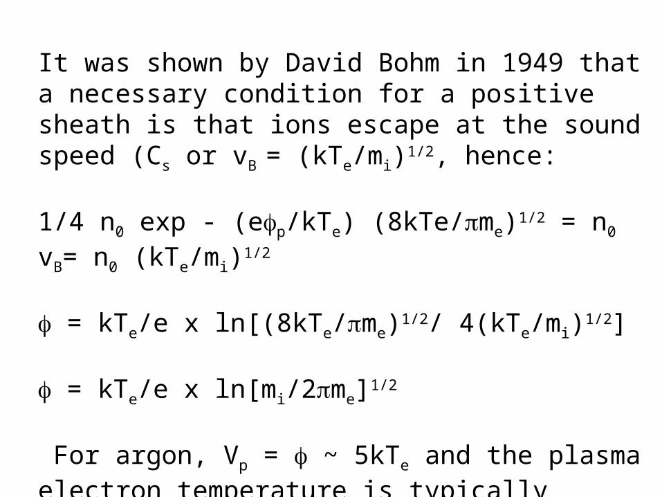
It was shown by David Bohm in 1949 that a necessary condition for a positive sheath is that ions escape at the sound speed (Cs or vB = (kTe/mi)1/2, hence:
1/4 n0 exp - (ep/kTe) (8kTe/me)1/2 = n0 vB= n0 (kTe/mi)1/2
= kTe/e x ln[(8kTe/me)1/2/ 4(kTe/mi)1/2]
= kTe/e x ln[mi/2me]1/2
For argon, Vp = ~ 5kTe and the plasma electron temperature is typically 30,000 K, ie. about 3 eV hence the plasma potential is 15 volts above the grounded walls.

Approximate derivation of the Bohm criterion following Severn
The boundary sheath maintains equal losses of positive and negative fluxes to the wall by decreasing the electron density by a factor of about 100, whereas the ion density decreases by much less.
So in the plasma at the beginning of the sheath the electron density gradient must be greater than the ion density gradient.
dni/dx < dne/dx
Severn takes x = 0 as being at the wall and negative x moving into the plasma ie. vi is negative.

Continuity equationdn/dt + d(nv)/dx = S+ - S-
if no sources or sinks S+ - S- = 0, and stationary flow (dn/dt = 0)then d(nv)/dx = 0
using partial derivativesv dn/dx = - n dv/dx
rearranging and considering only the ionsdni/dx =- ni/vi dvi/dx (because we want to make dni/dx go away)
We want to change this equation into: vi > (kTe/M)1/2 so we use the continuity and Boltzmann’s equations along with conservation of energy.Firstly, we get rid of dni/dx:

However, from the Sheath Criterion we see that the spatial ion gradient must be less than the spatial electron gradient so we can remove the dni/dx and introduce the inequality. Hence:
dni/dx = - ni/vi dvi/dx < dne/dxand rearranging:
- vi > ni (dvi/dx)/(dne/dx) A)
this gives us an inequality for the velocity.
now we now need to get the right hand side into some more manageable form (eg. the sound speed) using the Boltzmann equation and conservation of energy.
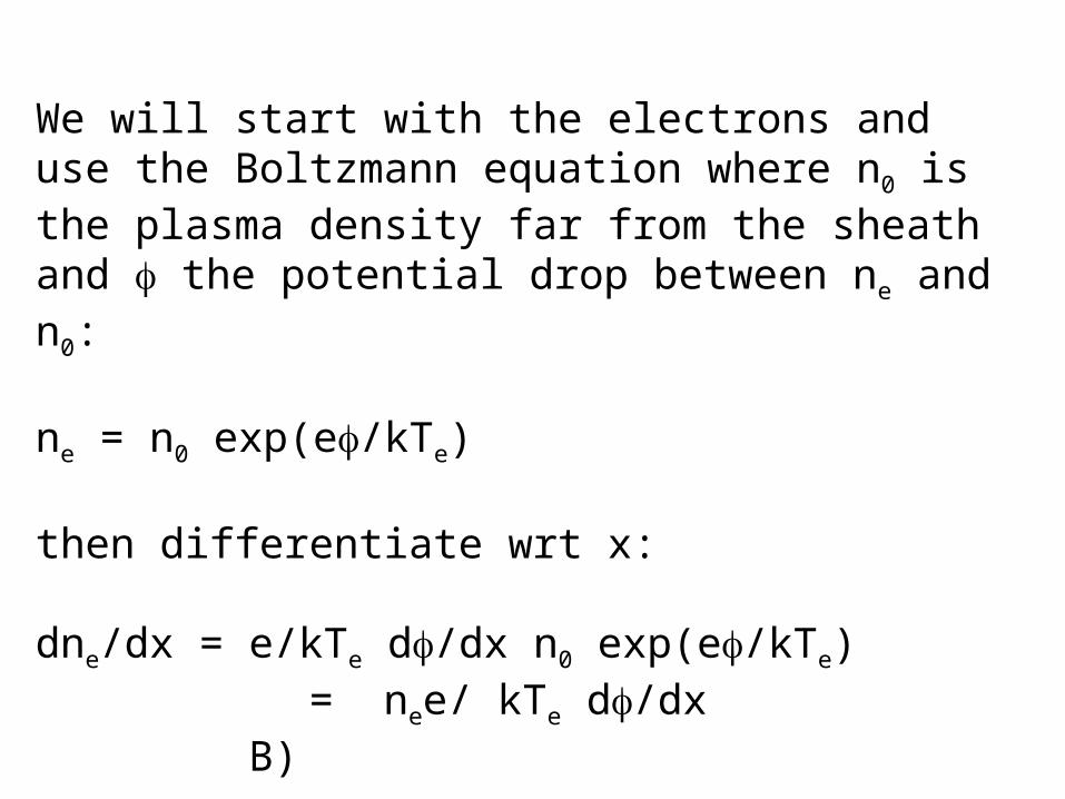
We will start with the electrons and use the Boltzmann equation where n0 is the plasma density far from the sheath and the potential drop between ne and n0:
ne = n0 exp(e/kTe)
then differentiate wrt x:
dne/dx = e/kTe d/dx n0 exp(e/kTe) = nee/ kTe d/dx B)
so now we can get rid of dne/dx but we need to find another expression for d/dx. Why not potential energy!!!!

To treat the ions we consider the conservation of energy in the potential gradient:
d(e + 1/2Mivi2)/dx = 0
ie. ed/dx + Mividvi/dx = 0
and dvi/dx = e/Mivi d/dx C)
substituting for dvi/dx (C) and dne/dx (B) into the inequality A) and taking equal ion and electron densities at the sheath edge in the plasma (a wee kludge):
- vi > ni ( ed/dx kTe)/(e ne Mivi d/dx)

- vi > ni ( ed/dx kTe)/(e ne Mivi d/dx)
cancelling gives
(- vi2)1/2 > (kTe/M)1/2
ie: vi > (kTe/M)1/2 not forgetting negative x moving into the plasma ie. vi is negative.

A note on plasma existence
If the plasma potential is 15 Volts and the ionisation potential for, say, argon is 15.75 eV, then all electrons that can ionise will only have one pass through the plasma before they are lost. Hence for the plasma to exist, it would be best if the plasma potential were somewhat greater than 15.75 Volts.

A note on electron energy probability functions
Electrons less energetic than Vp will be trapped and more energetic electrons will escape.
Trapped electrons will have many collisions and will form a Maxwellian distribution up to Vp.
Free electrons have an energy greater than Vp and their distribution reflects the heating mechanism

A consequence of the high electron mobility is that a plasma is a very good electrical conductor and will not happily support electric fields. The potential difference between the plasma and the walls is taken up in a thin region next to the walls called a sheath (since it protects the plasma from the walls).
If a potential more positive than Vp is applied to an electrode, it will remove electrons until the plasma is once again a potential of Vp higher than this electrode. If a negative potential is applied then a larger sheath forms on the electrode but the potential of the plasma is unchanged. The
thickness of the “Child-Langmuir” sheath in this case is given by:
Sheaths around electrodes

The sheath is not a plasma as the density of electrons is not equal to the density of ions, the difference in charge creating the sheath potential. As well as reflecting the majority of electrons back into the plasma the sheath accelerates the ions onto the electrode and this can be used to sputter material for coating onto adjacent targets, accelerate active species to a silicon wafer clamped to the electrode to produce reactive ion etching, to implant ions into the sub-surface layers and to densify growing film of SiO2 for example.
The sheath can be considered as a capacitor and it stores energy the same as a capacitor. Energy = 1/2 CV2

Calculate plasma density from input power
Consider a box with sides of 20 cm. And we create an argon plasma in it with 100 Watts of power and assume the electrons have a temperature Te = 3 eV. The power coming out of the plasma has to equal the power ‘in’.
Escaping from the plasma are ions and electrons in equal amounts, photons and radicals. We will neglect the radical contribution as it is normally less than 10% of the total power coming from electron energy loss in breaking molecular bonds.

Consider the ions; each ion that leaves and hits a wall takes the ionisation energy (Ei) and the energy it gains falling down the plasma potential (Vp = 5kTe).
Electrons are lost at the same rate as the ions and take 2kTe each.
Photons (one visible of 2 eV and a UV photon of 12 eV) are lost at the same rate as the ions since the cross section for excitation is approximately the same as that for ionisation.
Power ‘out’= Area x current (flux) x voltage = 6 x 0.2 x 0.2 x np x e x vB x (Ei + Vp + Eex + 2kTe)
= 0.24 x np x 1.6 x 10-19 x2.5 x 103 x (15 + 15 + 14 + 6)= 50 x 10-16 x np = power ‘in’= 100
np = 2 x 10¹⁶ m-3
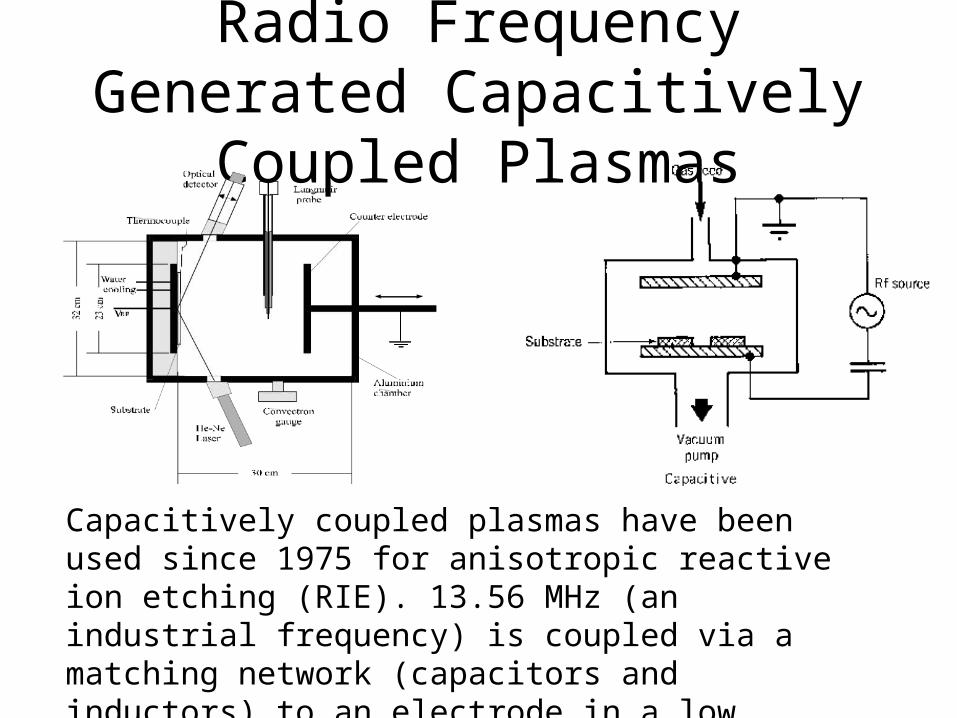
Radio Frequency Generated Capacitively Coupled Plasmas
Capacitively coupled plasmas have been used since 1975 for anisotropic reactive ion etching (RIE). 13.56 MHz (an industrial frequency) is coupled via a matching network (capacitors and inductors) to an electrode in a low pressure reactive gas such as CF4 or SF6.

Capacitively coupled plasma reactor
~
Cload Ctune
Matching Network Plasma
Powered electrode sheath capacitance
C1
Earthed electrode sheath capacitance
C2
The area of the powered electrode is generally much smaller than the earthed electrode (the walls of the vacuum vessel) hence the sheath protecting the plasma from the electrodes is smaller and the capacitance of the sheaths is smaller.
Coaxial connector

Potentials in a symmetric parallel plate reactor with a varying voltage applied to the powered electrode.
+Vrf
-Vrf
+0.5Vrf
0Vp
With no plasma we have a simple capacitor with potentials given by the dashed lines.
Electrons move toward positive potential on electrodes and create a more positive potential by their absence
electrons move toward positive potential
electrons move toward positive potential

Potentials in a symmetric parallel plate reactor with a varying voltage applied to the powered electrode.
+Vrf
-Vrf
+0.5Vrf
0 Vp ~ 5kTe ~ 15 volts for equal fluxes to the electrodes
With a plasma and 0 volts rf applied to the electrode, the plasma sits at a positive potential which decreases the escaping electron flux until it is equal to the escaping ion flux: Vp ~ 5kTe ~ 15 volts for a 3 eV argon plasma. At +Vrf electrons flow into the powered electrode until the potential is 5kTe above Vrf causing a sheath of 5kTe + Vrf on the ground electrode. As the rf voltage decreases, the potential of the plasma decreases until it reaches 5kT e. Further
lowering the voltage produces a sheath on the powered electrode, but the plasma potential remains at 5kT e.

System voltages, symmetric systemIf we take 100 Watts of input rf power (P) and a system impedance (Z) of 50 then the voltage (V) at the input to the matching network is given by: Vrms = (PZ)0.5 ~ 70 Volts.Hence Vrf = 1.4 x Vrms ~ 100 Volts.
The matching network is a resonant system with a quality factor of typically Q = 5, hence at the output of the matching network, the Vrf is multiplied by a factor of five resulting in Vrf ~ 500 Volts and it is this voltage which is applied to the electrode.

In the plasma we can generally ignore the plasma resistance and concentrate on the two capacitors in series, C1 and C2 represented by the sheaths on the powered and earthed electrodes. In the symmetric system, the size of the two sheaths is about the same so they have equal capacitances.
The plasma impedance is given by Z = 1/C1 + 1/C2 and since the capacitances are equal, the applied voltage is divided equally between the two sheaths.

Potentials in a symmetric plasmafor rf frequencies lower than the transit time for an ion to cross the sheath

Potentials in a symmetric plasmafor rf frequencies higher than the transit time for an ion to cross the sheath
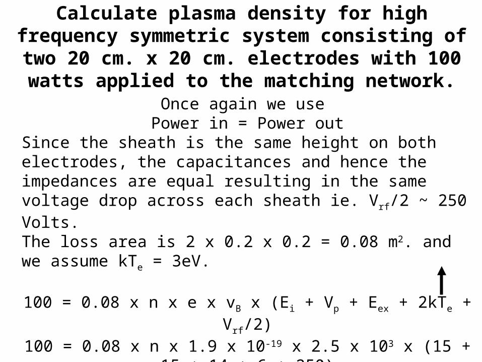
Calculate plasma density for high frequency symmetric system consisting of two 20 cm. x 20 cm. electrodes with
100 watts applied to the matching network.
Once again we use Power in = Power out
Since the sheath is the same height on both electrodes, the capacitances and hence the impedances are equal resulting in the same voltage drop across each sheath ie. Vrf/2 ~ 250 Volts. The loss area is 2 x 0.2 x 0.2 = 0.08 m2. and we assume kTe = 3eV.
100 = 0.08 x n x e x vB x (Ei + Vp + Eex + 2kTe + Vrf/2)100 = 0.08 x n x 1.9 x 10-19 x 2.5 x 103 x (15 + 15 + 14 + 6 + 250)
Hence: n = 1016 m-3
This is less than the density calculated for the 6 sided box because ions lose power in falling through the rf sheaths.

An introduction to asymmetric capacitively coupled discharges
Most capacitively coupled systems have a single powered electrode, the chuck.
The area of the chuck is much lower than the total area of the inside of the reactor.
Interestingly, as the pressure is increased, the plasma is more and more restricted to the volume just above the chuck and will appear, electrically, to be a symmetric system!

System Voltages in an asymmetric system,one powered and five sides at earth
Clearly, the capacitance of the sheath on the earthed electrode is five times larger in area than the sheath on the powered electrode. The plasma impedance is given by Z = 1/C1 + 1/C2 and since C2 > 5C1, most of the applied potential should be dropped across the powered electrode.
rf earth

Since most of the applied potential is be dropped across the powered electrode and the plasma is a good conductor, the whole of the plasma will oscillate following the voltage on the powered electrode.
For our 100 Watt plasma with a Q = 5, this will make the plasma near the powered electrode, and all the plasma, oscillate to over 500 Volts positive. Hence there will be a drop of 500 volts all around the earthed walls of the reactor.
Consequently, the sheath on the earthed walls is being forced to be at 500 volts but its impedance requires it to have only a few 10s of Volts and it will break down, like overvolting a 10 volt capacitor with a 500 volt power supply.
Note, we assume that the rf is connected directly to the powered electrode, there is no matching network, or there is no blocking capacitor in the matching network.

Sparks and the blocking capacitorAs the plasma is a good conductor, electrons will move from the region of the earthed sheath to the region of the powered sheath to short circuit the electric fields.
The sheath on the earthed electrode will be overvoltaged and the sheath capacitance will break-down in a spark.
These micro-discharges have an energy given by 0.5 CV2
The earthed sheath capacitance C = A/d = 8.8 10-12(Fm-1) / 10-4 ~ 10-7 FaradsThis is HUGE!!So energy stored is: 0.5 10-7 x 5002 ~ 10 mJoules
This is sufficient to melt little craters of about 50 metres in the metal walls.
Which is rather distressing as evaporated material from the wall will enter the plasma and change its properties as well as the properties of the wafers being processed.

Formation of a self bias voltageFortunately, there is a blocking series capacitor (tune) in the matching network and this charges up negatively to Vrf thereby allowing the plasma potential to revert to its equilibrium value of around 15 Volts. This voltage is called the self bias because it is created automatically by the plasma in an attempt at self preservation. For the 100 Watts of input power, the Vbias = Vrf = 500
Plasma Breakdown
2Vrf
Vbias

Charging a capacitorVC is Voltage across capacitor C which has a charge Q
VC = Q/C and I = dQ/dt
V0 = VR + VC and VR = IR hence: = IR + Q/C = RdQ/dt + Q/C
Q = CV0[1 - exp(-t/RC)] or
VC = V0[1 - exp(-t/RC)]
Approximate with a Taylor series:
VC = V0[1 -1 -t/RC + 1/2(t/RC)2……]
Hence for small time VC t

Capacitor Charging revisited
Linear for small timesSaturation for longer times
Rearranging the equations of the previous page:dQ/dt Q
ie. the rate of change of stuff depends on the amount of stuff

Capacitor discharging
For small times when shut off bias:
I = V/R and I is the ambipolar current flowing to the capacitor:I = AnevB = V/R
where A is the area of the rf chuck, n is the plasma density, e is the electronic charge 1.6 x 10⁻¹⁹ Coulombs and vB is the Bohm velocity or the ion sound speed (kTe/mi). Hence:
V (Te)1/2
So, if you pulse the bias voltage off you can measure the electron temperature

Plasma density for high frequency asymmetric box consisting of a 20 cm. powered electrode and the other 5 walls at earth
potential. 100 watts applied to the matching network.
Power in = Power outHere the sheath on the powered electrode can be considered as a DC sheath at the bias voltage Vbias = Vrf = 500 Volts. The voltage on the sheath on the earthed sides of the box is about the plasma potential Vp ~ 15 Volts if we assume kTe = 3eV.Assume the plasma density is constant over the volume.
Powered electrode area 0.2 x 0.2 = 0.04m2. Earthed electrodes area = 5 x 0.04 = 0.2m-2
Power out = n x 1.6 x 10-19 x 2.5 x 103 x [0.04(50 +500) +0.2(50 )]100 = n x 4 x 10-16 x [22 + 10]
n = 7.8 x 10¹⁵ m-3
ie. about 3 times less than the simple (inductive) box

Sheath heating vs gamma discharges
Sheath heating is simply the result of the collision of a light object with with a moving hard wall.eg. A game of tennis:
When the player hits the ball, it changes direction and acquires twice the velocity of the racket (4 times the energy)
In a plasma, the advancing sheath has to move at 108 cms-1 at least.
This can be approximated by assuming the sheath advances to its full extension in 1/4 of a rf cycle

A blast from the past
ANU 1D particle in cell simulation circa 1987

Newer PIC agrees with experiment at Bochum
watch the red electrons!

In Gamma discharges, fast ions generate secondary electrons on the substrate that subsequently, are accelerated by the electric field of the chuck bias.
Mean free path for ionisation imfp = 1/n is the ionisation cross section that can be taken to be ~ 1 to 3 10-16 cm-2, ie. 1 to 3 Å2. n is the neutral density.
For 1 mTorr, n = 3.4 1013 cm-3 hence imfp ~ 100 cm
For 100 mTorr imfp ~ 1 cm

Frequency effects in simple RC circuitfollowing Howling 1995
Assume the CCP is symmetric, ie equal sheaths on each electrode, hence the sheath capacitances are equal Ct = Cw = C
and the plasma presents a simple resistance R.
Vrf2/Pp = [R2 + (2/C)2]/R ~ 4/2C2R = f()
Assuming C and R do not change with frequency (false but not too bad) and that plasma impedance R is small cf. sheath
impedance 1/ C (good).
Hence the Vrf decreases with the frequency squared, for constant power.
Vrf 1/

Is this true??Use experiments and PIC simulation done by: W. Schwarzenbach, A. A. Howling,a) M. Fivaz, S.
Brunner, and Ch. HollensteinW. Schwarzenbach, A. A. Howling,a) M. Fivaz, S. Brunner, and Ch.
Hollenstein, J. Vac. Sci. Technol. A 14(1), 132, 1996
130 mm
The rf screen is adjusted so that Vdc = 0, ie. symmetric dischargerf power remains constant at 14 Watts and frequency varied from 13.56 to 70 MHz, argon pressure 100 mTorr with 50 sccm.

Ion energy measured by the Hiden is proportional to the Vrf, agrees with the PIC too.
Showing that the square of the applied Vrf divided by the applied power is approximately inversely proportional to the applied frequency squared
Vrf2/Pp ~ 4/2C2R

As the applied frequency increases, ion energy decreases and the plasma density increases. Hence the total power out will remain equal to the power in.

Notes on capacitive and inductive dischargesTypically, capacitively coupled plasmas have a skin depth that is much greater than the dimensions of the system and in analysis, the speed of light is assumed to be infinite
the skin depth is the distance required for the field at an interface to fall off by 1/e, examples would be total internal reflection of light on the surface of water and microwave ovens. In conductors, the rf current flows in the skin of the conductor, not the bulk.
~ c/pe for collisionless systems and where the rf frequency is much greater than the electron neutral collision frequency. (1/rf)1/2 for collisional systems rf << en
at 1 mTorr en ~ 107 and for 13.56 MHz rff ~ 108 >> en
but at 100 mTorr en >> rf hence collisional.

Evanescent wavesAssume wave propagates as E = E0expi(t - kz) normally, k = kr + iki the sum of the real and imaginary partsif k is purely imaginary ie. k = iki, no real wavelength kr = 0.
Then E = E0expi(t - ikz) ie. E = E0exp(it) x exp- ki
A temporally oscillating field with an exponentially decreasing amplitude.
water
air
microwave oven
stuff to be heated

Skin depth for low pressure plasma a few mTorr and 5 x 1010 cm-3
pe ~ 2 x 10⁴ x (ne)1/2 ~ 1.3 x 10⁹
~ c/pe ~ 3 x 10¹⁰/1.3 x 109 ~ 20 cm.
ie. close to the plasma dimension for either of the LAM reactors and and hence we would expect inductive effects, even with a CCP.
From Howling’s system, we would expect that the splasma would behave inductively for frequencies greater than 70 MHz. since the ion energy is then equal to the simple plasma potential and the plasma density would scale proportionally with the power.

E to H to W transition in the large “helicon” plasma WOMBAT
In E mode n P1/2 in H mode n P in W mode n exponential

What are the important impedances involved?Plasma resistance R is typically about 1 to 2 Ohms for densities of 1011 cm-3 measured at ANU and elsewhere.
Sheath impedance depends on area of reactor and sheath width.Taking Howling’s reactor with 13.56 MHz, Vb ~ Vion ~ 100Volts, electrode area A ~ x 6.52 ~ cm2. and power in ~ 10 Watts then calculate plasma density:10 = 2 x A x n x e x VB x( 100 +15 + 13 + 6 )10 = 2 x 43 x n x 1.6 x 10-19 x 2.5 x 105 x 132ie. n = 2 x 1010 cm-3
hence sheath width ~ 400x V3/4/(n1/2 x T1/4) cm ~ 0.07 cm.
capacitance of powered sheath: = A/d ~ 8.8 x 10-12 x 43 x 10-4/7 x 10-4 ~ 52 pF
Impedance = 1/C ~ 1/(2 x x 13.56 x 106 x 52 x 10-12) ~ 200
ie. the capacitive impedance is much greater than the plasma resistance!

When does the change from capacitive to inductive occur?
To reduce the capacitive impedance; the excitation frequency, plasma density and electrode area need to be increased.Take a LAM reactor with electrode diameter 13” (area 0.1 m2), excitation frequency 60 MHz and the same plasma density.The capacitive impedance is reduced by the inverse frequency ratio (13.56/60 ~ 0.23) and the inverse area ratio (0.013/0.1 ~ 0.13)
ZC ~ 200 x 0.23 x 0.13 ~ 10
so the system is some 10% inductive and we would expect plasma to appear in surprising places.
NB. In a CCP the impedance is dominated by the largest impedance ie. the largest capacitor which is commonly found on the powered electrode.

So, if the CCP reactors are behaving like inductively coupled reactors, and the TCP reactors can behave like capacitively coupled reactors:
why does LAM have 2 different reactor designs???

Topics for Tuesday the 30th of September 2008
Review of frequency effects
Introduction to inductive heating
Introduction to etching: SF6 and SiliconSF6 and SiO2
Concepts of passivation

Etching involves the creation of a gas phase product thatis volatile and will not stick to the feature being etched. Firstly, gas phase plasma electron collisions produce theetchant species:
SF6 -> SF2 + 4F
gas phase fluorine and surface silicon spontaneously
react to create volatile SiF4
4F + Si -> SiF4

Role of the electrons and ions in silicon etching with SF6
The electrons in the plasma maintain the plasma and dissociate the SF6, at the periphery of the plasma the electrons attach to neutrals to form negative ions.
The ion neither help nor hinder deep silicon etching as can been seen from the ANU results, the French results and LAM results
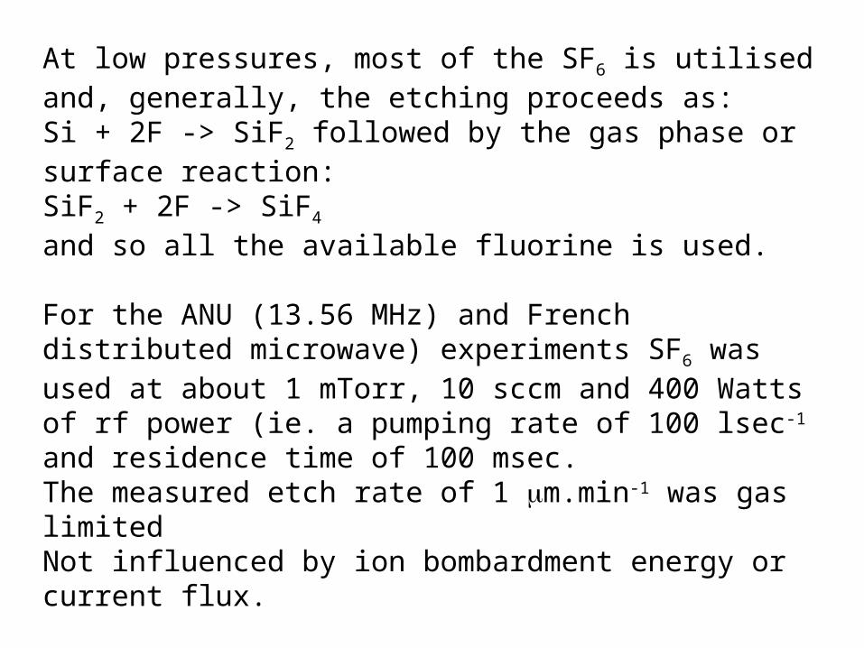
At low pressures, most of the SF6 is utilised and, generally, the etching proceeds as:Si + 2F -> SiF2 followed by the gas phase or surface reaction:SiF2 + 2F -> SiF4
and so all the available fluorine is used.
For the ANU (13.56 MHz) and French distributed microwave) experiments SF6 was used at about 1 mTorr, 10 sccm and 400 Watts of rf power (ie. a pumping rate of 100 lsec-1 and residence time of 100 msec.The measured etch rate of 1 m.min-1 was gas limited Not influenced by ion bombardment energy or current flux.
The etch was completely chemical and the profile was “isotropic”

Estimate power needed for dissociation of SF6:typically a covalent bond is about 2 eV (40,000 kiloCalories) but SF6 can absorb a lot of vibrational energy (20 eV??) so we take 10 eV for the production of the 4 atoms of fluorine.
10 sccm 10 x 2 x 1019/60 ~ 3 x 10¹⁸ molecules.sec-1
each molecule absorbs 10 eV, yielding power absorbedPSF6 ~ 1.6 x 10-19 x 10 x 3 x 1018
~ 5 watts ie, about 1% of the input power.
Nota bene: for some LAM systems, the SF6 flow is 500 sccm and then the power absorbed by the SF6 could be 250 Watts.
This would probably result in the incomplete dissociation of SF6 yielding SFx fragments that are not as active as atomic fluorine.

For low pressure etching we can account for all of the SF6 and atomic fluorine entering and leaving the system. For the previous example at ANU, actinometry of atomic fluorine showed that a full 4” wafer reduced the fluorine density by a factor of about 4, and that the etch product was SiF, hence it was not possible to etch faster.
stainless steel wafer
silicon wafer

However, by assuming the SiF picked up another 3 atoms of fluorine in the gas phase or on the walls of the reactor or in the pumping system to form SF4, then all the SF6 can be accounted for: entering, dissociating to yield 4 atoms of fluorine, etching to form SiF and subsequently SiF4 being pumped out. SF6 + Si -> SF2 + SiF4
In the LAM fast silicon etch systems (and other systems operating above about 5 mTorr) the etch rate is about 10 times slower at 10 m.min-1 at 100 Torr, AND the etch profiles suggest that the reactivity of the etchant is only 10%.
Why this is so is a bit of a mystery and we are working on it.
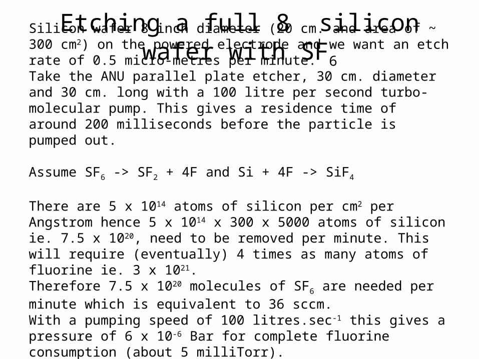
Etching a full 8” silicon wafer with SF6
Silicon wafer 8 inch diameter (20 cm. and area of ~ 300 cm2) on the powered electrode and we want an etch rate of 0.5 micro-metres per minute. Take the ANU parallel plate etcher, 30 cm. diameter and 30 cm. long with a 100 litre per second turbo-molecular pump. This gives a residence time of around 200 milliseconds before the particle is pumped out.
Assume SF6 -> SF2 + 4F and Si + 4F -> SiF4
There are 5 x 10¹⁴ atoms of silicon per cm2 per Angstrom hence 5 x 1014 x 300 x 5000 atoms of silicon ie. 7.5 x 10²⁰, need to be removed per minute. This will require (eventually) 4 times as many atoms of fluorine ie. 3 x 10²¹. Therefore 7.5 x 10²⁰ molecules of SF6 are needed per minute which is equivalent to 36 sccm.With a pumping speed of 100 litres.sec-1 this gives a pressure of 6 x 10⁻⁶ Bar for complete fluorine consumption (about 5 milliTorr). For safety (to remove fluctuations) usually take a 10 times higher flow.

The fluorine accounting suggests that a full 8” wafer etched at 5 m.min-1 would require 360 sccm of SF6 at 50 mTorr (with the same pumping speed of 100 l.sec-1). This assumes that flow fields and dissociation remain the same, BUT about 200 Watts would be absorbed by the SF6 so considerably more rf power would be required, some kiloWatts.
However, the pressure will have an effect: the plasma electrons will be cooled by the collisions and the electropositive plasma near the antenna (powered electrode) will be surrounded by an electro-negative plasma. Additionally, the fluorine atoms will suffer attaching collisions with various molecules and their density will decrease away from the visible (electro-positive) plasma.
Assuming fluorine atoms are very sticky (looking for an electron) then their mean free path at 100 mTorr would be about 1 cm.

Etch profiles and chemical etchingisotropic etching
Shaqfeh and Jurgensen Bell Labs 1989, solid angle subtended by the mask as seen on the etch face assuming etchant comes through the hole. Discovered the etch front propagates as a wave.

Use Mathematica (Bob Dewar) to calculate stream lines and etch front as a wave progressing into the silicon as a function of time. Assuming just chemical etching of silicon by fluorine. For great distances from the hole, etch rate cos/r2 due to flux conservation. The shape of the etch surface with a small hole is a sphere.
mask
Marcos, Rhallabi and Ranson in France used particle pushing and Monte/Carlo collisions to simulate the etch front for different sticking (etching efficiency) coefficient. Very similar to the analytical derivation.

Effect of sticking coefficient, basically fluorine usage
fluorine atom enters the hole and reflects from the far wall to the top where it sticks and subsequently etches. The smaller the sticking coefficient, the less overhang, ie. the shape becomes hemispherical rather than spherical. But the absolute etch rate drops.

Anisotropic etching of silicon requires sidewall protection
This is commonly achieved by an alternating deposition/etch proceedure eg. C4F8/SF6 or mixing in oxygen with SF6 to produce an oxide on the side walls. Fluorine etches oxide much slower than silicon and is reflected more easily from oxide.
fluorine atom
Hence the etch rate at the bottom of the via does not proceed as cos/r2 but should be proportional to the flux of fluorine arriving at the top of the hole.


