carbon nanotube modified electrodes for enhanced brightness in
TRANSCRIPT
1
Carbon nanotube modified electrodes for enhanced brightness in organic light emitting
devices
A.R. Inigo, J.M. Underwood and S.R.P. Silva*
Nanoelectronics Center, Advanced Technology Institute,
University of Surrey,
Guildford, GU2 7XH, Surrey, UK.1
Keywords: OLED, CNT, MWCNT, brightness, hole injection
ABSTRACT
Acid oxidized multiwall carbon nanotubes (COOH-MWCNT) have been introduced
as a hole injection buffer layer in an organic light emitting diodes (OLED). We show that the
OLED with COOH-MWCNT as a buffer layer provides higher brightness with lower
operating voltages. The addition of a COOH-MWCNT buffer layer has enabled a further
increase in the brightness of our OLED devices operating in excess of 20,000 cd/m2 due to
enhanced hole injection by several orders of magnitude. The increase in current injection and
brightness does not alter the optical emission spectrum at different operating voltages in these
devices. A model is proposed to explain this increase in current injection and brightness based
on the modified electron energy band alignment.
*Corresponding Author Email: [email protected]
2
1. Introduction
High quality OLEDs has been realised by designing multilayer structures with
balanced electron and hole injection, and efficient transport into the emitting layer using
specific transport materials [1]. N,N'-diphenyl-N,N~-bis(3 -methyl-phenyl)- 1,1’biphenyl-4,4
diamine (TPD) is one among the many favoured hole transport materials due to its ability to
act as a hole injector because of its favourable energy level positions at the anode [2,3].
Likewise, Tris(8-hydroxyquinolinato)aluminium (Alq3) is one of the few efficient electron
transport organic materials due to its relatively high electron mobility and its favourable
energy level positions at the cathode [4]. For better hole and electron injection, further
research is focussed on incorporating single wall (SW) and multiwall (MW) carbon nanotubes
(CNT) [5-8]. CNT have been introduced into the OLED structures in the form of composites
[9] or as a single layer from a solution functionalised CNT spin coated on to the top of an
anode [10] or spin coated prior to evaporation of the cathodes [11].
Indium tin oxide (ITO) which has a work function of ~4.7 eV is widely used as an
anode due to its high optical transmittance and high sheet conductance. A threshold barrier
height of ~0.3 - 0.4 eV or lower with respect to the adjacent hole transporting layer (HTL) is
required for the OLED to operate with space charge limited current (SCLC) and barriers
higher than 0.3 eV lead to injection limited current [12]. However, ITO’s work function of 4.7
eV produces a barrier height higher than 0.3 eV for most hole transporting materials which
have a highest occupied molecular orbital around 5.0 to 5.5 eV [12,13]. To overcome this
barrier, buffer layers such as copper phthalocyanine [6], poly(3,4-
ethylenedioythiophe):poly(styrenesulphonate) (PEDOT:PSS) and PEDOT:PSS:CNT
composites have been introduced between the ITO and the HTL [9,13]. Whilst the
performance improvements from these HTLs are moderate, the conventional HTLs have
shown to introduce other complexities into the device stack. The widely used PEDOT:PSS is
3
acidic in nature, known to affect the underlying ITO layer which is a major disadvantage.
Therefore, cheaper, solution processable HTL candidates such as CNTs show promise in this
regard.
While introduction of various HTLs have been demonstrated to give improved performance,
introduction of CNT as a barrier reduction buffer layer at the anode or at the cathode is still
untested and at the demonstration level. For example, the reference ITO/HTL/Alq3/Al have
demonstrated operation up to 15 to 20V with the highest luminance of 4000 cd/m2 at the
driving voltage of ~20V, and, with the introduction of PEDOT:PSS:MWCNT as an anode
buffer layer, the luminance increased up to 6500 cd/m2 at the driving voltage of ~16V with
the operating voltage of 10 to 16V [9]. Furthermore, CNT has been used as a cathode buffer
layer to achieve the maximum luminance of the reference device from ~1000 cd/m2 to ~5000
cd/m2 at the driving voltage of 15V with the operating voltage of 8 to 15V [11]. Here, we
present a green light emitting device with COOH-MWCNT as the buffer layer in between
ITO and the HTL.
In this work, OLEDs were fabricated with TPD as a hole transport layer and Alq3 as
an emitting layer. The reference ITO anode OLED has the device architecture of
ITO/TPD(35nm)/Alq3(35nm)/LiF/Al. OLED with ITO/COOH-MWCNT as an electrode has
the architecture of ITO/COOH-MWCNT/TPD(35nm)/Alq3(35nm)/LiF/Al. Hole only single
layer devices were also prepared with ITO/TPD(70nm)/Al and ITO/COOH-
MWCNT/TPD(70nm)/Al to compare the current injection characteristics with that of
corresponding OLEDs.
2. Experimental
2. 1 Acid functionalization of MWCNTs
4
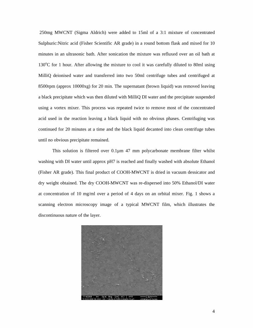
250mg MWCNT (Sigma Aldrich) were added to 15ml of a 3:1 mixture of concentrated
Sulphuric:Nitric acid (Fisher Scientific AR grade) in a round bottom flask and mixed for 10
minutes in an ultrasonic bath. After sonication the mixture was refluxed over an oil bath at
130oC for 1 hour. After allowing the mixture to cool it was carefully diluted to 80ml using
MilliQ deionised water and transferred into two 50ml centrifuge tubes and centrifuged at
8500rpm (approx 10000xg) for 20 min. The supernatant (brown liquid) was removed leaving
a black precipitate which was then diluted with MilliQ DI water and the precipitate suspended
using a vortex mixer. This process was repeated twice to remove most of the concentrated
acid used in the reaction leaving a black liquid with no obvious phases. Centrifuging was
continued for 20 minutes at a time and the black liquid decanted into clean centrifuge tubes
until no obvious precipitate remained.
This solution is filtered over 0.1µm 47 mm polycarbonate membrane filter whilst
washing with DI water until approx pH7 is reached and finally washed with absolute Ethanol
(Fisher AR grade). This final product of COOH-MWCNT is dried in vacuum dessicator and
dry weight obtained. The dry COOH-MWCNT was re-dispersed into 50% Ethanol/DI water
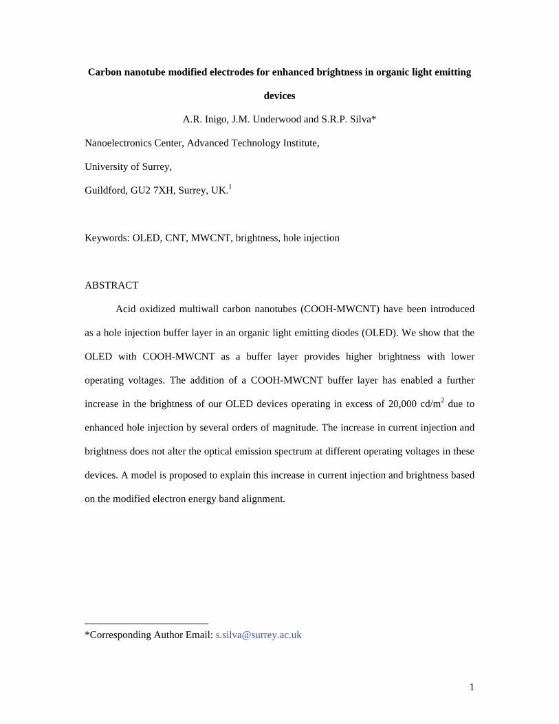
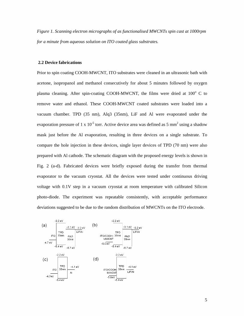
at concentration of 10 mg/ml over a period of 4 days on an orbital mixer. Fig. 1 shows a
scanning electron microscopy image of a typical MWCNT film, which illustrates the
discontinuous nature of the layer.
5
Figure 1. Scanning electron micrographs of as functionalised MWCNTs spin cast at 1000rpm
for a minute from aqueous solution on ITO coated glass substrates.
2.2 Device fabrications
Prior to spin coating COOH-MWCNT, ITO substrates were cleaned in an ultrasonic bath with
acetone, isopropanol and methanol consecutively for about 5 minutes followed by oxygen
plasma cleaning. After spin-coating COOH-MWCNT, the films were dried at 100o C to
remove water and ethanol. These COOH-MWCNT coated substrates were loaded into a
vacuum chamber. TPD (35 nm), Alq3 (35nm), LiF and Al were evaporated under the
evaporation pressure of 1 x 10⁻⁵ torr. Active device area was defined as 5 mm2 using a shadow
mask just before the Al evaporation, resulting in three devices on a single substrate. To
compare the hole injection in these devices, single layer devices of TPD (70 nm) were also
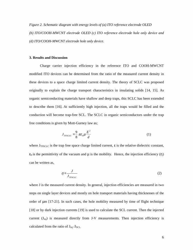
prepared with Al cathode. The schematic diagram with the proposed energy levels is shown in
Fig. 2 (a-d). Fabricated devices were briefly exposed during the transfer from thermal
evaporator to the vacuum cryostat. All the devices were tested under continuous driving
voltage with 0.1V step in a vacuum cryostat at room temperature with calibrated Silicon
photo-diode. The experiment was repeatable consistently, with acceptable performance
deviations suggested to be due to the random distribution of MWCNTs on the ITO electrode.
6
Figure 2. Schematic diagram with energy levels of (a) ITO reference electrode OLED
(b) ITO/COOH-MWCNT electrode OLED (c) ITO reference electrode hole only device and
(d) ITO/COOH-MWCNT electrode hole only device.
3. Results and Discussion
Charge carrier injection efficiency in the reference ITO and COOH-MWCNT
modified ITO devices can be determined from the ratio of the measured current density in
these devices to a space charge limited current density. The theory of SCLC was proposed
originally to explain the charge transport characteristics in insulating solids [14, 15]. As
organic semiconducting materials have shallow and deep traps, this SCLC has been extended
to describe them [16]. At sufficiently high injection, all the traps would be filled and the
conduction will become trap-free SCL. The SCLC in organic semiconductors under the trap
free conditions is given by Mott-Gurney law as;
d
EJTFSCLC
2
08
9 µεε= (1)
where JTFSCLC is the trap free space charge limited current, ε is the relative dielectric constant,
ε0 is the permittivity of the vacuum and µ is the mobility. Hence, the injection efficiency (η)
can be written as,
TFSCLCJ
J=η (2)
where J is the measured current density. In general, injection efficiencies are measured in two
steps on single layer devices and mostly on hole transport materials having thicknesses of the
order of µm [17-21]. In such cases, the hole mobility measured by time of flight technique
[18] or by dark injection currents [19] is used to calculate the SCL current. Then the injected
current (Jinj) is measured directly from J-V measurements. Then injection efficiency is
calculated from the ratio of Jinj /JSCL.
7
In the present study we have used a working OLED device configuration which has
the thickness around 70 nm. In TPD/Alq3 OLED, injection occurs from both electrodes;
anode and cathode. While the electron injection is the same in both devices, the hole injection
varies due to the modification of electrodes at the anode. So, the variation in injection
efficiencies can be assumed to be due to the presence of COOH-MWCNT modified ITO. To
avoid any ambiguity of these double carrier injection devices, we have fabricated hole only
devices of single layer TPD (70nm) with ITO and ITO/COOH-MWCNT anodes and Al as
cathode. TPD hole mobility, µhole= 10-3 cm2/Vs is used to determine the JSCL from equation
(2) [21].
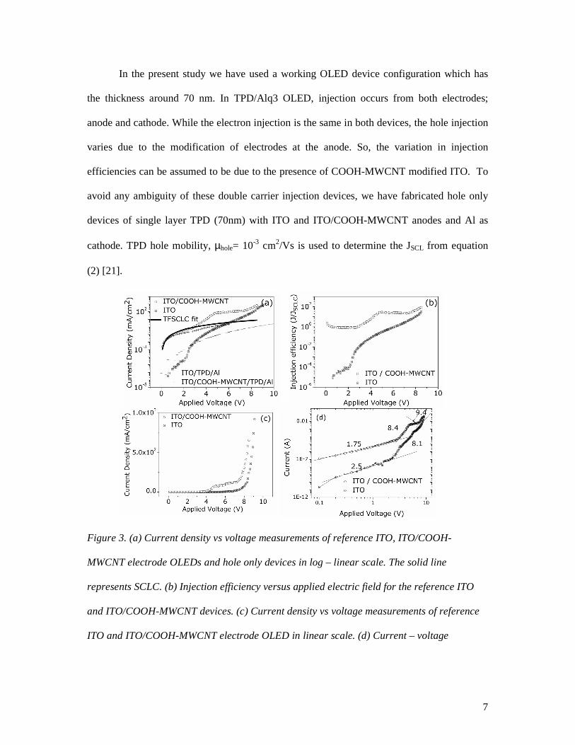
Figure 3. (a) Current density vs voltage measurements of reference ITO, ITO/COOH-
MWCNT electrode OLEDs and hole only devices in log – linear scale. The solid line
represents SCLC. (b) Injection efficiency versus applied electric field for the reference ITO
and ITO/COOH-MWCNT devices. (c) Current density vs voltage measurements of reference
ITO and ITO/COOH-MWCNT electrode OLED in linear scale. (d) Current – voltage
8
characteristics of ITO reference electrode OLED and ITO/COOH-MWCNT electrode OLED
in log-log scale to represent I α Vm behaviour, with fitted m values.
Fig. 3a shows the current density vs voltage (J-V) characteristics of JSCL, OLED and
hole only devices with reference ITO and ITO/COOH-MWCNT electrodes. OLED devices
follow the well established behaviour of OLEDs with an Alq3 emitter in which charge carrier
transport is trap charge limited SCLC. In these devices current – voltage (I-V) characteristics
was described by the power-law (I α Vm, Fig 3d) dependence for different exponent m with
variable operating regions ; before and after the on-set of EL [11]. This exponent m before the
onset of EL determines the type of contact and after the EL onset is determines the type of
bulk conductivity in Alq3 [22]. With voltages lower than the turn-on voltage, these devices
follow a power law dependence of m = ~2.5 and ~1.7 for the reference ITO and ITO/COOH-
MWCNT respectively and after turn on the reference ITO and ITO/COOH-MWCNT OLED
follows a power law dependence with m = ~8 [22].
While the J-V of ITO/TPD/Al devices varies significantly from the calculated JSCL,
ITO/COOH-MWCNT/TPD/Al devices showed a closer match. This indicates that
ITO/COOH-MWCNT electrodes enhances hole injection into TPD. Work function
measurements on ITO and ITO/COOH-MWCNT by our group [23] using Kelvin probe
method which confirms the ITO/COOH-MWCNT/TPD barrier height is within the required
threshold barrier height for SCLC ( i.e. 0.3 to 0.4 eV). Lower current density and high barrier
height of ~0.7 eV in the reference ITO electrode devices indicated the current injection is
limited by this high electrode barrier [24, 25].
Fig. 3b shows the charge carrier injection efficiency in the reference ITO and COOH-
MWCNTs modified ITO OLEDs which was determined from the ratio of the measured
current density in these devices to a space charge limited current density. It is noted that the
9
injection efficiency in COOH-MWCNTs modified ITO OLEDs is a few orders of magnitude
higher at lower applied voltages. This would facilitate achieving OLED operation at very low
voltages. For example a current density of 5 mA/cm2 is injected at ~3.7 V in the ITO/COOH-
MWCNT OLEDs in comparison to a reference ITO OLEDs which has a voltage which is
35% larger at ~5V. It should also be noted that the band discontinuity of 0.4 eV shown
between the ITO/ COOH-MWCNT and TPD in Fig. 2(b) is further modified due to the high
aspect ratio of the MWCNT. Much like in the case of electron field emission [6, 26]. There
will be field enhancement around the MWCNT which will further lower any barrier at the
interface. Due to this very high injection, the effective mobility appears to attain a value of 10-
3cm2/Vs or higher in the composite COOH-MWCNT modified ITO devices.
In addition to high charge carrier injection efficiency, there is a cusp observed from
applied voltage of 4 to 7 V in the J-V characteristics of COOH-MWCNT modified ITO
OLED (Fig. 3c and 3d). The observation of this kind of cusp has been reported earlier in the
literature as an anomalous current-voltage characteristic leading to a “negative differential
resistance (NDR)” for different types of organic materials [27-29]. These were observed due
the charge carrier transport through localised states formed in TPD (generally in organic
semiconducting materials) [27]. The origin and the associated charge transport properties of
these localised states are not well identified, but affected by the device thickness and
temperature [27]. Furthermore, the higher current during this initial turning on of the device
does not give rise to corresponding significant increase in light output and there is no
correlation between the current in the NDR region and the electroluminescence
characteristics. The reproducible nature of J-V ruled out the possibility of the burnt-shunt
effect reported in the devices in the literature [27] and this equally applies to the features
observed with our COOH-MWCNT modified ITO OLEDs. Recently, devices with NDR
have been reported with iodine or nitrogen doped TPD/Alq3 bilayer devices [28, 29]. The
10
NDR was not observed with iodine doped TPD single layer devices, but exhibited higher
current density than that of undoped devices. This behaviour would be expected if the NDR is
a minority carrier phenomenon where a high current density would mask such a phenomena
occurring in a parallel pathway [30, 31]. Higher current injection in single layer device was
attributed to the charge transport through the hopping sites in TPD and the additional hopping
sites created by the doping of iodine or nitrogen. In bilayer devices of TPD/Alq3, the
appearance of NDR behaviour was explained by proposing the emission of phonons during
the recombination process from the highly energetic holes travelling through doping induced
hopping sites and electrons from Alq3 [28,29]. These phonons led to the scattering of charge
carriers and decrease in the current with increasing applied voltage. In order to investigate the
two step turn-on phenomena, attempts were made to fit Fowler-Nordheim model to the two
turn on regions which resulted in poor fits, confirming that although the structure has a
discontinuous buffer layer, the effect is composite, and the relevance of existing models is
speculative and does not fully elucidate the phenomenon occurring in our films. [32]
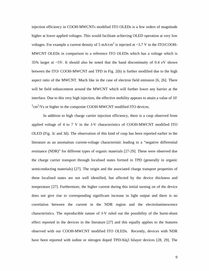
Figure 4. (a) Luminance vs voltage characteristics of reference ITO and ITO/COOH-
MWCNT electrode OLED and (b) Electroluminescence spectra of ITO/COOH-MWCNT
OLEDs where the voltage is ramped from 6.0 V to 9.5V (in steps of 0.5V).
11
Fig. 4a shows the luminescence vs voltage characteristics of reference ITO and
ITO/COOH-MWCNT OLED. Among these devices the reference device exhibits the highest
luminance of 30,434 cd/m2 (~ 9.1 V), while ITO/COOH-MWCNT OLED has a recorded
highest luminance of 20,562 cd/m2 (~ 8.5 V) respectively. It is also observed that the
ITO/COOH-MWCNT OLED has a higher luminance than that of the reference ITO OLED at
voltages between 3 – 8 V. Since the device is operated under a continuous applied voltage
mode with a step voltage of 0.1 V, the device shows evidence of degradation due to joule
heating with extended times. ITO/COOH-MWCNT OLED device turns-on (1 cd/m2) around
2.8 V while the reference ITO OLED turns on at slightly higher voltage of 3.1. The light
output of ITO/COOH-MWCNT OLED devices is not well correlated with the current
densities through the region with lower voltage turn-on, similar to devices reported with NDR
behaviour. For example, at the applied voltage of 5.3V, ITO/COOH-MWCNT OLED
exhibits luminance of 235 cd/m2 (71 mA/cm2), while the reference ITO OLED has its
luminance of ~84 cd/m2 (2.45 mA/cm2); which are equivalent to ~3 times increase in light
emission intensity and about ~30 times increase in current density. If we assume the external
quantum efficiency of the device to be of the order of 1.5%, then the expected increase in
light emission intensity would be less than 50% (as opposed to 300%). The huge increase in
the light output will be discussed in terms of higher charge injection, more localised radiative
recombination and better transport through the device structure as a result of the CNT
incorporation as a hole injection layer.
Fig. 4b shows the electroluminescence spectra of ITO/COOH-MWCNT electrode
OLED which are characteristic of Alq3 OLED with the emission peak around 530 nm. Since
the electroluminescence from the ITO reference and ITO/COOH-MWCNT OLED are similar,
the electroluminescence of reference ITO OLED was not shown in the figure for clarity (but
available in the supporting information). Although the ITO/COOH-MWCNT OLED devices
12
exhibit different exponent values in J-V curves after turn on, the spectra at different applied
voltages do not have a significant spectral shift or the appearance of new emission peaks
compared with the references. These spectra confirm that the presence of COOH-MWCNT
with the corresponding lower turn on region do not change the emission characteristics of
Alq3 devices and the emission is confined to the Alq3 layer. This is also in agreement with
earlier reports that the HTL TPD does not contribute to the light emission [16, 28].
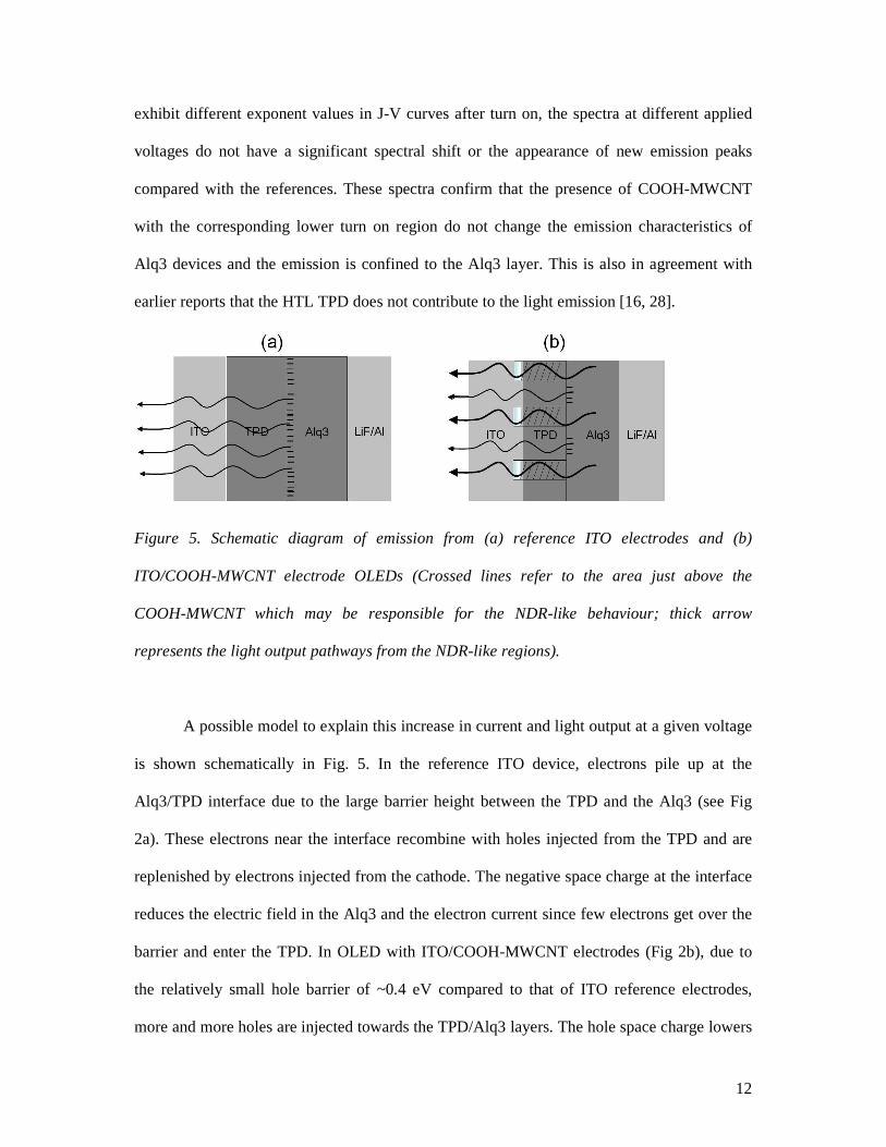
Figure 5. Schematic diagram of emission from (a) reference ITO electrodes and (b)
ITO/COOH-MWCNT electrode OLEDs (Crossed lines refer to the area just above the
COOH-MWCNT which may be responsible for the NDR-like behaviour; thick arrow
represents the light output pathways from the NDR-like regions).
A possible model to explain this increase in current and light output at a given voltage
is shown schematically in Fig. 5. In the reference ITO device, electrons pile up at the
Alq3/TPD interface due to the large barrier height between the TPD and the Alq3 (see Fig
2a). These electrons near the interface recombine with holes injected from the TPD and are
replenished by electrons injected from the cathode. The negative space charge at the interface
reduces the electric field in the Alq3 and the electron current since few electrons get over the
barrier and enter the TPD. In OLED with ITO/COOH-MWCNT electrodes (Fig 2b), due to
the relatively small hole barrier of ~0.4 eV compared to that of ITO reference electrodes,
more and more holes are injected towards the TPD/Alq3 layers. The hole space charge lowers
13
the electron barrier. This barrier height reduction enables more electrons to enter the TPD
layer and recombine with the holes. This leads to higher electron current through the Alq3 and
higher total current. This assumption is supported by the observation of lower external
quantum efficiency, because there is now more non-radiative recombination taking place in
the TPD layer than that of reference ITO electrode OLED. This can be balanced in the future
by increasing the electron transport in the device or moving the recombination pathway away
from the TPD to the Alq3. High electron concentration throughout the Alq3 layer results in
recombination more evenly spread in the Alq3 layer. This leads to the observation of higher
overall luminance in ITO/COOH-MWCNT electrode OLED at any given applied voltage
compared with the reference ITO electrode devices. Earlier reports from our group on hole
only devices of ITO/SWCNT/TPD(100 nm)/Al suggests that the TPD morphology is
modified by the presence of COOH-MWCNT on the top of ITO [9]. TPD on to the top of ITO
appears to have a more crystalline regime just above the COOH-MWCNT, compared to that
of TPD on the top of the ITO. Fig 5b depicts the situation where the TPD morphology is
modified due to the presence of COOH-MWCNT. In the TPD crystalline phases, the lower
barrier for electrons may enable electrons to enter the TPD where they may recombine with
holes non-radiatively. Therefore, the build-up of electrons at the interface is prevented (Fig 5)
and there is a subsequent increase in electric field within the Alq3.
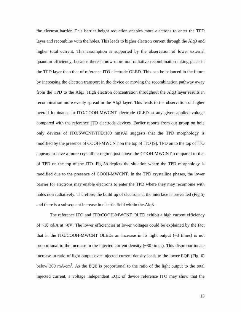
The reference ITO and ITO/COOH-MWCNT OLED exhibit a high current efficiency
of ~18 cd/A at ~8V. The lower efficiencies at lower voltages could be explained by the fact
that in the ITO/COOH-MWCNT OLEDs an increase in its light output (~3 times) is not
proportional to the increase in the injected current density (~30 times). This disproportionate
increase in ratio of light output over injected current density leads to the lower EQE (Fig. 6)
below 200 mA/cm2. As the EQE is proportional to the ratio of the light output to the total
injected current, a voltage independent EQE of device reference ITO may show that the
14
conduction process is not injection-limited [19]. While the barrier height of ~0.7eV at the
ITO/TPD suggests the current is injection limited in the reference devices [24], the voltage
independent EQE could also be due to a balanced of injection in holes and electrons. While
the voltage dependent EQE of the ITO/COOH-MWCNT OLED may initially appear to
indicate that the conduction process is injection limited (electron in this case), the barrier
height of ~0.4eV at the ITO/ COOH-MWCNT interface and SCLC fitting suggests that the
conduction process is not. This voltage dependent EQE is likely to be influenced by the
enhanced hole injection with respect to applied electric field in the ITO/COOH-MWCNT
OLEDs. The basic conclusion of our model, enhanced hole injection efficiency with
ITO/COOH-MWCNT is corroborated by the EQE measurements.
Figure 6. External quantum efficiency of reference ITO and ITO/COOH-MWCNT electrode
OLED. Lower efficiency in the NDR like region is attributed to the disproportionate ratio of
current injection (30 times) to luminance (3 times) in ITO/COOH-MWCNT OLED
The lower EQEs at lower current densities are attributed to the non-optimum carrier
recombination in the Alq3 layer and due to the lower level of electron mobility and lower
electron injection compared to that of the improved holes in the ITO/COOH-MWCNT
15
OLED. There is no one to one correlation to the increase in light output to the increase in
holes passing through the material. We believe this is due to the unavailability of sufficient
electrons [20]. It may be possible that some electrons might get in to the TPD regions due to
SCLC effects as discussed earlier and might recombine non-radiativley. It is more important
that the radiative recombination only occurs in Alq3 and not in TPD.
4. Conclusions
The presence of COOH-MWCNT at the anode increases hole injection, which has an
immediate impact even at low voltages and can be used to mitigate against previous device
architectures which were limited by poor hole injection from ITO reference devices. Though
the presence of COOH-MWCNT creates localised states and space charge in the TPD that has
the effect of lowering the barrier to electron flow between the Alq3 and TPD, the radiative
recombination takes place within the Alq3 and the emission spectrum is not affected. The
appearance of NDR-like phenomena and its effective utilisation in device performance needs
further detailed investigation and can be a useful tool for future designers.
Acknowledgements
This research was partly funded by a portfolio partnership award by the EPSRC, U.K.,
and by E.ON AG, as part of the E.ON International Research Initiative. Responsibility for the
content of this publication lies with the authors.
References
[1] Baldo MA, O’Brian DF, You Y, Shoustikov A, Silby S, Thomson ME, Forrest SR.
Highly efficient phosphorescent emission from organic electroluminescent devices. Nature
1998; 395: 151-4.
16
[2] Weaver MS, Bradley DDC. Organic electroluminescence devices fabricated with
chemical vapour deposited polyazomethine films. Synth. Met. 1996; 83b: 61-6.
[3] Gao XC, Cao H, Huang CH, Li BG, Ibrahim K, Liu FQ, Umitani S.
Electroluminescence from both a light-emitting layer and hole transport layer: spectral
evidence for charge carrier tunneling injection. Chem. Phys. Lett. 1998; 297: 530-6.
[4] Chen BJ, Lai WY, Gao ZQ, Lee CS, Lee ST, Gambling WA. Electron drift mobility
and electroluminescent efficiency of tris(8-hydroxyquinolinolato) aluminium. Appl. Phys.
Lett. 1999; 75: 4010-12.
[5] Dai L. Light-emitting polymers and carbon nanotube electron emitters for
optoelectronic displays. Smart Mater. Struct. 2002; 11: 645-51.
[6] Hatton RA, Blanchard NP, Stolojan V, Miller AJ, Silva SRP. Nanostructured copper
phthalocyanine-sensitized multiwall carbon nanotube films. Langmuir 2007; 23: 6424-30.
[7] Blanchard NP, Hatton RA, Silva SRP. Tuning the work function of surface oxidised
multi-wall carbon nanotubes via cation exchange. Chem. Phys. Lett. 2007; 434 : 92-5.
[8] Aguirre CM, Auvray S, Pigeon S, Izquierdo R, Desjardins P, Martel R. Carbon
nanotube sheets as electrodes in organic light-emitting diodes. Appl. Phys. Lett. 2006; 88
183104.
[9] Wang GF, Tao XM, Wang RX. Fabrication and characterization of OLEDs using
PEDOT:PSS and MWCNT nanocomposites. Comp. Sci and Tech 2008; 68: 2837-41.
[10] Tan LW, Hatton RA, Latini G, Shannon JM, Silva SRP. Modification of charge
transport in triphenyldiamine films induced by acid oxidized single-walled carbon
nanotube interlayers. Nanotechnology 2008; 19: 485706.
[11] Liu D, Fina M, Guo J, Chen X, Liu G, Johnson SG, Mao SS. Organic light-emitting
diodes with carbon nanotube cathode-organic interface layer. Appl. Phys. Lett. 2009; 94:
013110.
17
[12] Davids PS, Campbell IH, Smith DL. Device model for single carrier organic diodes.
J. Appl. Phys. 1997; 82:6319-26.
[13] So SK, Tse SC, Tong KL. Charge Transport and Injection to Phenylamine-Based Hole
Transporters for OLEDs Application. J. Disp. Tech. 2007; 3: 225-232.
[14] Rose A. Space-Charge-Limited Currents in Solids. Phys. Rev. 1955; 97: 1538-44.
[15] Lambert MA. A simplified theory of two-carrier, space-cgarge-limited current flow in
solids. .RCA Review 1959; 20: 682.
[16] Burrows PE, Shen Z, Bulovic V, McCarthy DM, SR Forrest, Cronin JA, Thompson
ME. Relationship between electroluminescence and current transport in organic
heterojunction light‐emitting devices. J. Appl. Phys. 1996; 79: 7991-8006.
[17] Antoniadis H, Miller JN, Roitman DB, Cambell IH. Effects of hole carrier injection
and transport in organic light-emitting diodes. IEEE Transactions on Electron Devices
1997; 44: 1289-94.
[18] Ioannidos A, Facci JS, Abkowitz MA. Evolution in the charge injection efficiency of
evaporated Au contacts on a molecularly doped polymer. J. Appl. Phys. 1998, 84: 1439-
45.
[19] Tse SC, Tsang SW, So SK. Polymeric conducting anode for small organic
transporting molecules in dark injection experiments. J. Appl. Phys. 2009; 100: 063708,
[20] Shen Y, Jacobs DB, Mallaras G, Koley G, Spencer MG, Ioannidis. Modification
of Indium Tin Oxide for Improved Hole Injection in Organic Light Emitting Diodes.
Adv. Mater. 2001; 13: 1234-1238.
[21] Kaliniwski J, Palilis LC, Kim WH, Kafafi ZH. Determination of the width of the
carrier recombination zone in organic light-emitting diodes. J. Appl. Phys. 2003; 94:
7764-8.
18
[22] Lambert MA, Mark P. Current Injection in Solids. Academic, New
York, 1970.
[23] Wu CC, Chun JKM, Burrows PE, Sturm JC, Thomson ME, Forrest SR, Register AR.
Poly(p‐phenylene vinylene)/tris(8‐hydroxy) quinoline aluminum heterostructure light
emitting diode. Appl. Phys. Lett.1995; 66: 653-5
[24] Hatton RA, Blanchard NP, Tan LW, Latini G, Cacialli F, Silva SRP. Oxidised carbon
nanotubes as solution processable, high work function hole-extraction layers for organic
solar cells. Org. Electron. 2009; 10: 388-95.
[25] Campbell AJ, Bradley DDC, Laubender J, Sokolowski M. Thermally activated
injection limited conduction in single layer N,N8-diphenyl-N,N8-bis.3-methylphenyl.1-18-
biphenyl-4,48-diamine light emitting diodes. J. Appl. Phys.1999; 86: 5004-11.
[26] Miller AJ, Hatton RA, Silva SRP. Interpenetrating multiwall carbon nanotube
electrodes for organic solar cells. Appl. Phys. Lett. 2006; 89:133117.
[27] Berlab S, Brutting W, Schwoerer M. Anomalous current-voltage characteristics in
organic light-emitting devices. Synth. Met. 1999; 102:1034-37.
[28] Fanga YK, Chiang YT, Chen SF, Lin CY, Hou SC, Hung CS, Tsai TY, Chang SH,
Chou TH. Observation of room temperature negative differential resistance (NDR) in
organic light-emitting diode with inorganic dopant. J. Phys. & Chem. Solids 2008; 69:
738-41.
[29] Chou TH, Chen SF, Fang YK, Hou CS, Lin FS, Lin CY. Significantly Improved
Luminance of Organic Light-Emitting Diodes by Doping Iodine and Nitrogen Treatment.
Jpn. J. Appl. Phys. 46; 2007 :2753-57.
19
[30] Bhattacharyya S, Henley SJ, Mendoza E, Gomez-Rojas L, Allam J, Silva SRP.
Resonant tunnelling and fast switching in amorphous-carbon quantum-well structures.
Nat. Mater. 2006; 5: 19-22.
[31] Chan KK, Silva SRP, Amartunga G. Electronic properties of semiconducting
diamond-like carbon-diamond . Thin Solid Films 1992; 212: 232-239.
[32] Oey CC, Djurixic AB, Kwong CY, Cheung CH, Chan WK, Nunzi JM, Chui PC.
Nanocomposite hole injection layer for organic device applications. Thin Solid Films
2005; 492:253-258 .