carrier transport phenomena in metal contacts to alingan-based
TRANSCRIPT

3
Carrier Transport Phenomena in Metal Contacts to AlInGaN-Based Laser Diodes
Joon Seop Kwak Department of Printed Electronics Engineering,
Sunchon National University, Maegok, Jeonnam, Korea
1. Introduction
High power AlInGaN-based laser diodes (LDs) have attracted great attention as light sources for high-density optical storage systems and micro-display systems, as well. One of the main concerns in this area is the fabrication of high-quality ohmic contacts to p-GaN with low resistance and thermal stability, since operation power of the AlInGaN-based LDs greatly affects the life time of the LDs.[1] Achieving low resistance ohmic contacts to p-GaN has been particularly challenging, because of difficulty in obtaining a hole concentration over 1018 cm-3 and the absence of metals having a work function higher than that of p-GaN (6.5 eV).[2]
For fabrication of AlInGaN-based LDs with low input power, free-standing GaN has attracted attention as a substrate because of its low dislocation density, high thermal conductivity, and easy cleaving.[3,4] Another advantage of using the GaN substrate is to fabricate devices with a backside n-contact. This allows the fabrication process to be simple and reliable, and reduces the size of devices, which increases yield in mass-production. Free-standing GaN substrate has two faces with a different crystal polarity, Ga- and N-face polarity, which greatly influence on the electrical properties at metal/GaN interface as well as those at AlGaN/GaN heterostructure.[5,6]
In order to achieve high-quality ohmic contacts to AlInGaN-based LDs, carrier transport phenomena at the interface between metal and p-GaN as well as n-GaN should be elucidated. This chaper discusses carrier transport phenomena in metal contacts to AlInGaN-based LDs, and also introduces a design to improve the operating voltage characteistics of the AlInGaN-based LDs based upon the carrier transport mechanism in metal contacts to AlInGaN-based LDs.
2. Carrier transport in metal contacts to p-GaN contact layer of AlInGaN LDs
Many experiments on the electrical characteristics of metal contacts to p-GaN have been carried out, mainly focusing on the variation of metallization scheme, alloying condition, and surface treatment.[7-11] In order to achieve the low-resistance ohmic contacts to p-GaN, carrier transport phenomena at the interface between metal and p-GaN should be elucidated. Kim et al. reported that surface treatment of the p-GaN shifted the Fermi level to
www.intechopen.com

Semiconductor Laser Diode Technology and Applications 30
an energy level near the valence band by removing oxide layer, resulting in the reduction of the barrier height for holes.[7] In addition, Jang et al. showed the increase in carrier concentration at the regions near the surface of p-GaN for the surface-treated p-GaN using the Hall-effect measurements, and suggested that field emission dominated current flow at the interface between non-alloyed Pt contact and the surface-treated p-GaN.[12]
2.1 Dependence of contact resistivity on hole concentration
In order to understand the carrier transport phenomena at the interface between the metal contacts and p-GaN contact layer of AlInGaN LDs, the dependence of contact resistivity on the hole concentration of ohmic contacts to p-GaN should be investigated, because carrier concentration is one of the most important factor to affect carrier transport at the metal-semiconductor interface.
The hole concentration and the concentration of Mg, [Mg] for a series of p-GaN films are shown in Fig. 1 as a function of flow rate of bis-(cyclopentadienyl)-magnesium (Cp2Mg). As shown in Fig. 1, the [Mg] increased with Cp2Mg and reached up to 1x1020 cm-3 when the flow rate of Cp2Mg was 2.8 μmole/min. The hole concentration initially increased from 7.5x10¹⁶ (sample A) to 2.2x1017 cm-3 (sample B) with the increase of the flow rate of Cp2Mg from 0.70 to 1.05 μmole/min. Further increase in the flow rate of Cp2Mg to 1.75 and 2.80 µmole/min, however, resulted in a significant decrease of the hole concentration to 1.2x10¹⁷
(sample C) and 2.0x1016 cm-3 (sample D), respectively. These results are well matched to the previous results, where the hole concentration initially increased with [Mg] and it decreased significantly with further increase in the [Mg].[13]
Fig. 1. The hole concentration and the [Mg] for a series of p-GaN films as a function of flow rate of Cp2Mg.
Figure 2 shows I-V characteristics of the non-alloyed Pd/Pt/Au contacts deposited on the series of p-GaN films with a different [Mg]. For the contacts on sample A having the lowest [Mg] among the samples as shown in Fig. 1, the measured current at 0.5 V between two metal pads with the gap spacing of 5 μm was 19 μA, and it increased to 41 and 54 μA for the contacts on sample B and C, respectively. In case of the contacts on sample D with the
0.5 1.0 1.5 2.0 2.5 3.02x10
19
4x10¹⁹
6x10¹⁹
8x10¹⁹
1x10²⁰
sample D
sample C
sample B
sample A
Flow Rate of Cp2Mg (µmole/min)
Concentr
atio
n o
f M
g (
cm
-3)
1016
1017
1018
Hole
Concentr
atio
n (
cm
-3)
www.intechopen.com

Carrier Transport Phenomena in Metal Contacts to AlInGaN-Based Laser Diodes 31
highest [Mg] and the lowest hole concentration, the current at 0.5 V was measured as 64 μA. It is worth to notice that the non-alloyed Pd/Pt/Au contacts deposited on samples A, B, and C displayed non-linear I-V curves, while I-V curve became linear for the contacts on sample D. This is suggestive of producing the better ohmic contact on sample D having the lowest hole concentration among the samples.
Fig. 2. I-V characteristics of the non-alloyed Pd/Pt/Au contacts deposited on the series of p-GaN films with a different [Mg].
The contact resistivity for the Pd/Pt/Au contacts on the p-GaN films having the different [Mg] is shown in Fig. 3. For comparison, the hole concentration as a function of the [Mg] is also displayed. The contact resistivity for the non-alloyed Pd/Pt/Au contacts on sample A having the [Mg] of 3x1019 cm-3 was 3.0x10⁻¹ Ω-cm2, and it was reduced to 8.9x10⁻² Ω-cm2 for the contacts on sample B, having the higher [Mg] than that of sample A. This can be attributed to the increase in hole concentration with the Mg until the [Mg] is 4.5x1019 cm-3, as shown in Fig. 3. The increase in the hole concentration reduces the barrier width as well as barrier height between the contact and the p-GaN, followed by the enhancement of carrier tunneling through the barrier and the reduction of contact resistivity, as shown in Fig. 3.[14]
In case of the Pd/Pt/Au contacts on sample C, however, the contact resistivity was further reduced to 3.2x10⁻² Ω-cm2, although the hole concentration of sample C (1.2x1017 cm-3) was lower than that of the sample B (2.2x1017 cm-3), as shown in Fig. 3. Furthermore, the contact resistivity for the contacts on sample D, having the lowest hole concentration among the samples (2.0x1016 cm-3), was significantly reduced to 5.5x10⁻⁴ Ω-cm2. This value is more than two orders of magnitude lower than that of the contacts on sample B having the highest hole concentration among the samples.
Figures 2 and 3 clearly show that the non-alloyed Pd/Pt/Au contacts on sample D, having the lowest hole concentration and the highest [Mg] among the samples, had the lowest contact resistivity among the samples and displayed the linear I-V relationship. The metal-semiconductor contact theory indicates that the decrease in carrier concentration increases contact resistivity, especially in field emission which is essential for obtaining ohmic behavior for the metal-semiconductor interface with high barrier height.[14,15] This implies that the
-0.5 0.0 0.5-50
-25
0
25
50
p-GaN(Mg)/Pd/Pt/Au
sample A
sample B
sample C
sample D
Curr
ent (µ
A)
Voltage (V)
www.intechopen.com

Semiconductor Laser Diode Technology and Applications 32
linear I-V relationship and the low contact resistivity of the non-alloyed contacts on sample D cannot be explained by the field emission in the metal-semiconductor contact theory.
Fig. 3. The contact resistivity for the Pd/Pt/Au contacts on the p-GaN films having a different [Mg]. The hole concentration as a function of the [Mg] is also displayed.
2.2 Influence of micro-structural defects on the carrier transport
One possible explanation for the reduction of contact resistivity of Pd/Pt/Au contacts as the hole concentration of p-GaN decreased when the [Mg] is higher than 4.5x1019 cm-3, as shown in Fig. 3, is the influence of microstructural defects such as dislocations on the carrier transport at the interface between the non-alloyed contact and p-GaN. High threading dislocation density, which is produced by large differences in lattice mismatch and thermal expansion between GaN and sapphire substrates, has a significant influence on the performance of InGaN light emitting devices.[16] The LEO method is a popular method used to reduce the threading dislocation density. The LEO method has been used to lower the threading dislocation density by more than two orders of magnitude.[17,18] Indeed, the use of LEO GaN has already increased the lifetime of InGaN LDs to more than 10,000 hours.[19,20]
The electrical characteristics of dislocations in n-GaN have been well studied. Weimann et al. suggested a model in which filled traps along dislocation lines act as Coulomb scattering centers, explaining the low transverse mobility in GaN by the scattering of electrons at charged dislocation lines.[21] Hansen et al. observed free surfaces of undoped GaN by scanning capacitance microscopy, and found the presence of excess negative charge in the region surrounding the dislocations, which implies the presence of deep acceptorlike trap states near the valence band associated with threading dislocations.[22]
The high dislocation density has also greatly affected electrical properties at p-n junctions. Kozodoy et al. examined the effect of dislocations on the reverse bias current density by comparing the reverse bias current for p-n diodes on LEO GaN with that for diodes on the dislocated GaN, and found that reverse-bias leakage current was reduced by three orders of
2x10¹⁹
4x10¹⁹
6x10¹⁹
8x10¹⁹
1x10²⁰
1016
1017
1018
Hole
Concentr
ation (
cm
-3)
10-4
10-3
10-2
10-1
100
sample D
sample C
sample B
sample A
Mg Concentration (atoms/cm3)
Conta
ct R
esis
tivity (
Ω-c
m2)
www.intechopen.com

Carrier Transport Phenomena in Metal Contacts to AlInGaN-Based Laser Diodes 33
magnitude on LEO GaN.[23] Kuksenkov et al. also showed that the dark current was correlated with dislocation density in GaN diodes.[24] However, scant information is available concerning the correlation between the high dislocation density and the electrical properties of ohmic contacts to p-GaN.
In addition, the effect of dislocation density on threshold current and life time of InGaN LDs were reported in several papers,[19,20,25] while, little results on the effects of dislocation density on the operating voltage of the InGaN LDs have been reported until now. Nam et al. reported that the lifetime of the InGaN LDs was greatly influenced by the operating voltage, although it is well known that the lifetime is affected by the operation current and the temperature of the LDs.[26]
To examine the influence of microstructure of p-GaN on carrier transport at the interface between the non-alloyed contact and p-GaN, Kwak and Park have focused on investigating the effect of dislocation on the contact resistivity of ohmic contacts on p-GaN through measurement of the I-V characteristics for non-alloyed Pd ohmic contacts on LEO GaN and on dislocated GaN. They fabricated TLM patterns with a very narrow mesa structure, which enabled the production of TLM patterns on LEO GaN and on dislocated GaN. They grew p-GaN films on c-plane sapphire substrates by metalorganic chemical-vapor deposition (MOCVD). Trimethylgallium (TMGa), trimethylindium (TMIn), and ammonia (NH3) were used as precursors for Ga, In, and N, respectively. The LEO process was performed to decrease the dislocation density of the layers. First, 2-μm-thick GaN layers were grown on the sapphire substrates. Second, silicon dioxide and metal masks were deposited on the GaN layer; striped patterns with widths of 4 μm and a periodicity of 10~18 μm were formed in the <1-100> direction of GaN using standard lithography and inductively coupled plasma reactive ion etching (ICP-RIE). Third, window areas of GaN layers were etched down to the sapphire substrate by ICP-RIE. Finally, the striped-pattern GaN wafers were loaded into the MOCVD reactor for the LEO process.
After the growth of LEO GaN, both the 2-μm-thick, Mg-doped, p-GaN layer and the laser diode structures with a 405 nm wavelength were grown on LEO GaN wafers. For p-GaN, bis-(cyclopentadienyl)-magnesium (Cp2Mg) was used as a precursor for Mg. the 2-μm-thick p-GaN layer had a Mg concentration of 2×1019 cm-3, where the hole concentration measured by the Hall measurement system was 7×1017 cm-3. In addition, an additional thin layer (10 nm) having a Mg concentration of 1×1020 cm-3 was grown on the 2-μm-thick p-GaN layer. Although the p-GaN having a Mg concentration of 1×1020 cm-3 had the hole concentration as low as 2×1016 cm-3, it can reduce the contact resistivity of the non-alloyed contacts to p-GaN significantly.[27]
For the InGaN-based laser diode, a Si-doped GaN layer was first grown on the LEO-GaN layer. Doped AlGaN/GaN superlattice structures and GaN were used as cladding and waveguide layers, respectively. The AlGaN/GaN superlattice structures consisted of 25-Å-thick AlGaN and 25-Å-thick GaN layers. The active layers were InGaN/InGaN MQW structures consisting of a 40-Å-thick In0.08Ga0.92N well and a 100-Å-thick In0.02Ga0.98N barrier. A Mg-doped, AlGaN, electron-blocking layer was grown between the active layer and the p-type waveguide layer. Finally, an additional thin layer (10 nm) having a Mg concentration of 1×1020 cm-3 was grown as a p-contact layer. Conventional annealing was conducted below 900 °C to achieve good p-type conduction for both samples.
www.intechopen.com

Semiconductor Laser Diode Technology and Applications 34
Fig. 4. Schematic diagrams showing the process flow for fabricating the narrow TLM patterns.
Fig. 5. SEM image of the fabricated narrow TLM patterns, having 2 μm-wide narrow mesa structures.
To investigate the effect of dislocation on the contact resistivity of ohmic contacts on p-GaN, Kwak and Park fabricated TLM patterns with a very narrow mesa structure (narrow TLM), which enabled the production of TLM patterns on LEO as well as on dislocated GaN. The narrow TLM patterns were fabricated as described in the process flow shown in Fig. 4. First, a chemically assisted ion beam method was used to etch a 2-μm-wide mesa stripe on the wing and seed regions of the LEO-GaN structures, as shown in Fig. 4(b). This was followed by deposition of the 0.2-μm-thick TiO2 passivation layer and 0.1-μm-thick Pd contacts, as shown in Fig. 4(c). Before deposition of the Pd contacts, the TLM patterns were etched in buffered HF solution, rinsed in DI water, and dried with nitrogen before being loaded into the vacuum system for metal deposition. Pd (100 nm) films were
seedu-GaN
LEOu-GaN
coalescenceboundary
p-GaN
TiO2
Pd
narrowmesa
structure
(a)
(b)
(c)
TLM on
seed GaN
TLM on
LEO GaN
TLM on coalescence
boundary
www.intechopen.com

Carrier Transport Phenomena in Metal Contacts to AlInGaN-Based Laser Diodes 35
deposited by electron beam evaporator. The Pd provides good specific contact resistance in the as-deposited state, therefore, Pd was used as an ohmic material to narrow TLM.[27,28] Figure 5 is a scanning electron microscope (SEM) image of the fabricated narrow TLM patterns with narrow (2-μm in width) mesa structures. The cross-sectional SEM image (inset) shows that the narrow TLM pattern was well fabricated on the wing region of the LEO GaN.
Figure 6 shows the I-V characteristics of the Pd contacts on the LEO GaN (low dislocation density region) as well as on the seed GaN (dislocated region) measured at a gap spacing of 10 μm. The Pd contacts, both on the LEO GaN and the seed GaN, produced linear I-V characteristics, as shown in Fig. 6. It is noteworthy that variations of the I-V characteristics of the contacts on the LEO GaN, as well as on the seed GaN, were small and identical, which implies that dislocation had little effect on the I-V characteristics of the Pd contacts.
Figure 7 shows the specific contact resistances of the Pd contacts on the LEO GaN and that of the contacts on the dislocated GaN, as measured using the narrow TLMs. The non-alloyed Pd contacts on the LEO-GaN (low dislocation density region) showed a specific contact resistance of 2~3Ì10-3 Ω-cm2. The contacts on the dislocated regions (both the seed and coalescence region) also showed a specific contact resistance of 2~3Ì10-3 Ω-cm2. In addition, the Pd contacts located between the LEO-GaN region and the dislocated regions had a specific contact resistance of 2~3Ì10-3 Ω-cm2. These results clearly showed that dislocation had little influence on the specific contact resistance of the non-alloyed Pd contacts on p-GaN.
Fig. 6. I-V characteristics of the Pd contacts on the LEO GaN as well as on the seed GaN measured at 10 μm gap spacing.
-0.50 -0.25 0.00 0.25 0.50-20
-10
0
10
20
Curr
ent
(µA
)
-0.50 -0.25 0.00 0.25 0.50-20
-10
0
10
20
Voltage (V)
Curr
en
t (µ
A)
Pd on seed GaN
Pd on LEO GaN
www.intechopen.com

Semiconductor Laser Diode Technology and Applications 36
Fig. 7. The specific contact resistances of the Pd contacts on LEO GaN and that of the contacts on dislocated GaN, as measured using narrow TLMs.
It has been reported that a neutral region is formed around each dislocation due to a mid-gap state, which reduces electron mobility of n-GaN.[29] The neutral region along the dislocations likely does not contribute to carrier transport through the metal/semiconductor (M/S) interface, which implies that the actual area at the M/S interface could be reduced. In our sample, however, the carrier concentration was relatively high (p=7.0x1017 cm-3), which is essential to InGaN based laser diodes, a smaller depleted area due to the dislocation was expected. Shiojima et al. evaluated the effect of dislocation on current-voltage (I-V) characteristics of Au/Ni/n-GaN Schottky contacts by using a submicrometer Schottky dot array formed by electron beam lithography, and showed that neither dislocations nor steps affected the I-V characteristics, which could be attributed to a relatively higher carrier concentration (n=5.8x1017 cm-3).[30] To confirm this explanation, however, further studies, such as the same experiment with low hole concentrations, are needed to estimate the actual area which contributes the carrier transport at the M/S interface.
To elucidate whether the dislocation affects the voltage characteristics of the InGaN LDs, we fabricated InGaN LDs, in which non-alloyed Pd contacts were produced on a 2- μm -width ridge waveguide structure. The location of the ridge waveguide varied from seed region to coalescence region. Figure 8(a) shows the variation of output power and voltage of the InGaN LDs as a function of injected current for the LDs with the Pd contacts on the LEO GaN and on the dislocated GaN. As shown in Fig. 8(a), the output power-current curve was differed greatly for the different locations of the Pd contacts. In contrast, the voltage-current curve changed little with the location of the contacts. Figure 8(b) displays the variation of the operating voltage at 50 mA and threshold current as a function of location of the ridge waveguide of the InGaN LDs. As shown in Fig. 8(b), the InGaN LDs, which have a ridge structure on the LEO-GaN region, showed a low threshold current of 55 mA. The threshold current of the LDs where the ridge structure is located between the seed and the LEO regions, however, increased to 90 mA. Furthermore, it increased as high as 119 mA in the seed region. This implies that dislocation has a significant influence on the threshold current
10-3
10-2
TLM on
ELO GaN TLM including
coalescence
boundary
TLM between
seed and
ELO GaN
TLM on
seed GaN
Conta
ct R
esis
tivity (
Ω-c
m2)
www.intechopen.com

Carrier Transport Phenomena in Metal Contacts to AlInGaN-Based Laser Diodes 37
characteristics of InGaN LDs. These results agree well with previous reports. It was reported that an increase in dislocation density significantly deteriorated the operating current characteristics of the InGaN LDs.[26] A significant increase in nonradiative recombination in the dislocation region may cause a significant increase in the threshold current of the dislocated region of the InGaN LDs, as shown in Fig. 8.[31]
(a) (b)
Fig. 8. (a) Variation of output power and voltage of the InGaN LDs as a function of injected current for the LDs with the Pd contacts on the LEO GaN and the dislocated GaN, and (b) variation of the operating voltage at 50 mA and threshold current as a function of location of the ridge waveguide of the InGaN LDs.
The density of dislocation, however, had minimal influence on the operating voltage of the ridge waveguide InGaN LDs. As shown in Fig. 8(b), we obtained 5.8 V as the operating voltage at 50 mA for the LEO-GaN region of LDs. Similar operating voltage values were obtained even for the dislocated regions of LDs. This can be attributed to the results shown in Fig. 7, where the density of dislocation had little influence on the specific contact resistance of the non-alloyed Pd contacts. These results clearly suggest that dislocation exerts significant influence on the threshold current of InGaN LDs, but has minimal influence on the specific contact resistance of the contacts to p-GaN.
2.3 Influence of deep level defects on the carrier transport
Another possible explanation for the abnormal dependence of the contact resistivity on the hole concentration observed in this study is the influence of deep level defects in p-GaN on the carrier transport at the Pd/p-GaN interface. Götz et al. reported the presence of compensating deep centers in Mg-doped GaN using capacitance spectroscopy.[32] Bayerl et al. also detected a deep level defect named MM1 located near the mid gap using optically detected magnetic resonance and observed different defect signals for p-GaN with different [Mg].[33] Hofmann et al. suggested that the structure of MM1 center could be a nitrogen vacancy-Mg pair defect (VN-MgGa).[34] In addition, Shiojima et al. found that carrier capture and emission from acceptor-like deep level defects caused depletion layer width to vary significantly in Ni contacts to p-GaN.[35]
40 60 80 100 120 140 160
0
1
2
3
4
5
6
7
8
9
10
0
1
2
3
4
5
6
7
8
9
10
Vo
lta
ge
(V
)
Ou
tpu
t P
ow
er
(mW
)
Current (mA)
LD on LEO GaN
LD on LEO GaN and seed GaN
LD on seed GaN
40
60
80
100
120
Th
resh
old
Cu
rre
nt
(mA
)4
5
6
7
8
LD on
seed GaN
LD on
LEO GaN and
seed GaN
LD on
LEO GaN
Vo
lta
ge
at
50
mA
(V
)
www.intechopen.com

Semiconductor Laser Diode Technology and Applications 38
Kwak et al. have examined the temperature-dependent contact resistivity of non-alloyed Pd/Pt/Au contacts to p-GaN films as well as the temperature-dependent sheet resistivity of the p-GaN films, in order to understand the anomalously low contact resistivity (~10-4 Ω-cm2) considering the large work function difference between the metal and p-GaN and the abnormal dependence of contact resistivity on carrier concentration, as well. In their study, three different p-GaN samples having a different Mg concentration, [Mg], were used (samples A, B, and C). A thin buffer layer and a 1-um-thick undoped GaN layer on a sapphire substrate was grown by the MOCVD, followed by the growth of 1-um-thick p-GaN layers having three different [Mg]. Variation of [Mg] in p-GaN was conducted by changing the flow rate of bis-(cyclopentadienyl)-magnesium. Sample A, B, or C has the [Mg] of 4.5x10¹⁹, 7.5x10¹⁹, or 1.0x1020 cm-3, respectively, which was measured using secondary ion mass spectroscopy. The hole concentration of the sample A, B, or C was determined as 2.2x10¹⁷, 1.2x10¹⁷, or 2.0x1016 cm-3, respectively, which was obtained from Hall-effect measurements. These results indicate that the hole concentration decreased as increase in the [Mg] in the p-GaN films in this study. The temperature dependence of the contact resistivity and the sheet resistance were performed in a cryostat using transfer length method (TLM). Prior to the fabrication of the TLM patterns, mesa structures were patterned using chemically assisted ion beam etching with Cl2. Then, they were etched in buffered HF solution, rinsed in DI water, and dried with nitrogen before being loaded into the vacuum system for metal deposition. Pd (20 nm)/Pt (30 nm)/Au (80 nm) films were deposited by electron beam evaporator.
Fig. 9. The temperature dependence of contact resistivity of the non-alloyed Pd/Pt/Au contacts on the p-GaN samples having the different [Mg]. The [Mg] of the samples A, B, and C were 4.5x10¹⁹, 7.5x10¹⁹, and 1.0x1020 cm-3, respectively, and the hole concentration of the samples A, B, and C were 2.2x10¹⁷, 1.2x10¹⁷, and 2.0x1016 cm-3, respectively
The temperature dependence of contact resistivity of the non-alloyed Pd/Pt/Au contacts on the p-GaN samples having the different [Mg] is shown in Fig.9. As the measured temperature decreased, as shown in Fig. 9, the contact resistivity of the Pd/Pt/Au contacts
0 5 10 15 20 2510
-4
10-3
10-2
10-1
100
101
Co
nta
ct
Re
sis
tivity (
Ω-c
m2)
1000/T (1/K)
non-alloyed
Pd/Pt/Au contacts on
[Mg]=4.5x10¹⁹
/cm3
[Mg]=7.5x10¹⁹
/cm3
[Mg]=1.0x10²⁰
/cm3
www.intechopen.com
Carrier Transport Phenomena in Metal Contacts to AlInGaN-Based Laser Diodes 39
on the p-GaN samples rapidly increased. For the contacts on sample C having the [Mg] of 1x1020 cm-3, the contact resistivity increased from 5.5x10⁻⁴ to 4.0x10⁻² Ω-cm2, as the temperature decreased from 300 to 100 K. In case of the contacts on the sample A or B, the contact resistivity also increased by more than one order of magnitude as the temperature decreased from 300 to 100 K. These results clearly show that the carrier transport at the Pd/p-GaN interface is not dominated by pure-tunneling mechanism because it implies a temperature-independent contact resistance.[15] It is worthwhile to note that the contact resistivity of the non-alloyed Pd/Pt/Au contacts on the sample C (5.5x10⁻⁴ Ω-cm2) having a low hole concentration of 2.0x1016 cm-3 was anomalously low at room temperature, considering the large work function difference between Pd and p-GaN. In addition, in a temperature region higher than 75 K, the contact resistivity of the contacts on the sample C having the lowest hole concentration (2.0x1016 cm-3) was more than one order of magnitude lower than that of the contacts on the sample A or B having a higher hole concentration (2.2x10¹⁷ or 1.2x1017 cm-3, respectively). This is abnormal since the metal-semiconductor contact theory indicates that the decrease in carrier concentration increases contact resistivity.[15]
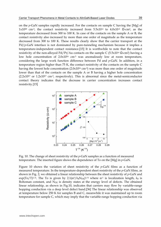
Fig. 10. The change of sheet resistivity of the p-GaN samples as a function of measured temperature. The inserted figure shows the dependence of To on the [Mg] in p-GaN.
Figure 10 shows the variation of sheet resistivity of the p-GaN films as a function of measured temperature. In the temperature-dependent sheet resistivity of the p-GaN films, as shown in Fig. 2, we obtained a linear relationship between the sheet resistivity of p-GaN and exp(To/T)1/4. The To is given by 2.1(α3/kBNDE)1/4 where α-1 is localization length, kB is Boltzman constant, and NDE is density states at the energy level of defects. The obtained linear relationship, as shown in Fig.10, indicates that carriers may flow by variable-range hopping conduction via a deep level defect band.[36] The linear relationship was observed at temperature below 250 K for samples B and C, meanwhile it was maintained up to room temperature for sample C, which may imply that the variable-range hopping conduction via
0.23 0.24 0.25 0.26 0.27 0.28 0.29
100
101
102
103
4 6 8 10100
120
140
To
[Mg] (1019
cm-3)
To1/4
Resis
tivity (
Ω-c
m)
T-1/4
(K-1/4
)
sample A
sample B
sample C
www.intechopen.com

Semiconductor Laser Diode Technology and Applications 40
a deep level defect band still dominates current flow at room temperature for sample C. The linear relationship between sheet resistivity and exp(To/T)1/4 was also reported in low-temperature grown (LTG) GaAs, in which a dense EL2-like deep defect band was produced.[37]
The figure inserted in Fig. 10 shows the dependence of To on the [Mg] in p-GaN. As the [Mg] increased from 4.5x10¹⁹ to 1.0x1020 cm-3, as shown in the inserted figure, the To was reduced from 130 to 106, which implies that the defect density increased as the [Mg] in p-GaN increased since To is 2.1(α3/kBNDE)1/4. It is worthy of note that we can calculate the defect density, NDE, from the obtained To value, if we know localization length, α-1. However, since the localization length of the deep level defect band in the p-GaN films has not been reported yet, we could not obtain the defect density of the p-GaN. Instead, we can estimate the defect density in the p-GaN films having the different [Mg] using the relation between contact resistivity and defect density,[38] which is given by
2 1/3 1/3 exp( )/ exp( / )(3 / 4 )
Bc
D DE DE DE
qk T
kTq k h aN N N
ϕρ
γ π=
Θ − (1)
where ΘD is Debye temperature, γ is constant, a is extent of the wave function, and qφ is the barrier height between the metal and the deep level defect. Figure 11 shows the variation of contact resistivity as a function of defect density calculated from the Eq. (1). As shown in Fig. 11, contact resistivity rapidly decreases as increase in the defect density, and it also decreases when the qφ decreases. In order to obtain the defect density in the p-GaN films, the qφ was measured by using the devised I-V method which utilizes large-area contacts and reverse-biased I-V characteristics,[39] and the measured qφ was 0.36 eV. From the measured
Fig. 11. The variation of contact resistivity as a function of defect density and barrier height between metal and the deep level defects, qφ, which is calculated from the eq. (1). The measured qφ and the obtained contact resistivity for the Pd/Pt/Au contacts on samples A. B, and C were also depicted.
1x10¹⁹
2x10¹⁹
3x10¹⁹
4x10¹⁹
5x10¹⁹
10-5
10-4
10-3
10-2
10-1
100
101
Pd/Pt/Au
contacts on
sample A
sample B
sample C
Φb= 0.30 eV
Φb= 0.35 eV
Φb= 0.40 eV
Φb= 0.45 eV
Φb= 0.50 eV
Con
tact R
esis
tivity (
Ω-c
m2)
Defect Density (cm-3)
www.intechopen.com

Carrier Transport Phenomena in Metal Contacts to AlInGaN-Based Laser Diodes 41
qφ and the contact resistivity of the Pd/Pt/Au contacts on the p-GaN having the different [Mg], as shown in Fig. 11, we obtained the defect densities in the sample A, B, and C as 1.4x10¹⁹, 1.6x10¹⁹, and 2.9x1019 cm-3, respectively. It should be noted that the defect density in the p-GaN increased as increase in [Mg] in the p-GaN, which is well matched to the relation between To and [Mg], as shown in the inserted figure in Fig. 10.
Based on these results, the band diagram of a Pd/p-GaN contact was devised, as shown in Fig. 12. The deep defect level, EDE, is unoccupied with electrons in most of the material, as shown in Fig. 12. However, because of the band bending near the interface between the metal and the p-GaN, occupied region in the deep defect level was produced by the electrons moved from the metal. The occupied region of the deep defect level, which is located below the Fermi level, EF, as shown in Fig. 12, may allow the carriers to flow from the metal directly to the dense deep defect level in the p-GaN, which results in predominant current flow at the Pd/p-GaN interface through the deep level defect band, rather than the usual valence band. The carrier transport at the metal/p-GaN interface through deep level defects is also observed in the Ni/p-GaN interface. Shiojima et al. found that carrier capture and emission from acceptor-like deep level defects caused depletion layer width to vary significantly in Ni contacts to p-GaN.[40] In addition, Yu et al. reported a tunneling component in the Ni contacts to p-GaN due to the defect states located in the near surface region of the semiconductor.[41]
Fig. 12. Band diagram of the Pd/p-GaN in which the carriers flow from the metal directly to the dense deep level defects.
From the devised band diagram, as shown in Fig. 12, the abnormal dependence of the contact resistivity on the carrier concentration, as shown in Fig. 9, as well as the anomalously low contact resistivity (5.5x10⁻⁴ Ω-cm2) of the Pd/Pt/Au contacts on sample C considering the large work function difference between Pd and p-GaN and the low hole concentration of sample C (2.0x1016 cm-3) can be explained as follows. In the samples A, B and C, when the [Mg] in the p-GaN films increased from 4.5x10¹⁹ to 1.0x1020 cm-3, the hole concentration decreased from 2.2x10¹⁷ to 2.0x1016 cm-3, meanwhile the deep level defect density increased from 1.4x10¹⁹ to 2.9x1019 cm-3, as shown in Fig. 11. The increase in the defect density allows more carriers to flow from the Pd to the p-GaN through the deep level defects, followed by the reduction of the contact resistivity. This can result in the abnormal
Pd
EVBM
EF
EDE
ECBM
p - GaN
-----
www.intechopen.com

Semiconductor Laser Diode Technology and Applications 42
dependence of the contact resistivity on the carrier concentration, that is, the decrease in the contact resistivity from 8.9x10⁻² to 5.5x10⁻⁴ Ω-cm2 even though the hole concentration was reduced from 2.2x10¹⁷ to 2.0x1016 cm-3. Furthermore, the unexpectedly low contact resistivity (5.5x10⁻⁴ Ω-cm2) even though the hole concentration was as low as 2.0x1016 cm-3 can be attributed to the large defect density in the sample C (2.9x1019 cm-3), since the very large defect density can greatly lower the contact resistivity, as shown in Fig. 12. The anomalously low contact resistivity considering a low carrier concentration in semiconductors is also observed in non-alloyed ohmic contacts to LTG GaAs, which was explained by the predominant current flow at the metal/LTG GaAs interface through a very large concentration (~3x1019 cm-3) of EL2-like deep defect level, followed by a low contact resistivity of 1.5x10⁻³ Ω-cm2 even though the carrier concentration was less than 1011 cm-
3.[38] As for the deep level defects in the p-GaN films, the energy level and structure of the deep defect are not clearly understood yet. One possible acceptor-like deep defect level is an impurity band. Cheong et al. suggested that Mg acceptors formed an impurity band that had thermal activation energy in a range of 300-360 meV.[42] Clarifying the deep defect level seems to be the key issue to a deeper understanding of the carrier transport at the metal/p-GaN interface, which remains for further study.
Finally, The experimental results and theoretical calculation suggested that a deep level defect band having a large defect density over 1019 cm-3 existed in the p-GaN films and the density of the deep level defects was enlarged as the [Mg] increased. The unexpectedly low contact resistivity (~10-4 Ω-cm2) considering the large work function difference between the metal and p-GaN as well as the abnormal dependence of the contact resistivity on the hole concentration could be explained by the carrier transport model in which the carriers flow from the metal directly to the dense deep level defects.
2.4 Design of p-GaN contact layer to minimize operating voltage of AlInGaN LD
Based on the understanding of carrier transport phenomena in metal contacts to p-GaN contact layer, a p-GaN:Mg contact layer can be designed to minimize the operating voltage of AlInGaN LD. As for the design of p-GaN:Mg contact layer, Kwak et al. reported the p-GaN contact layer having a high Mg-doped thin cap layer.[27,43,44] In this design, an additional thin layer (10 nm) having a high [Mg] (1x1020 cm-3) was grown on p-GaN having the [Mg] of 4.5x1019 cm-3. In x-ray diffraction, the full width at half maximum values of (0002) and (1ī02) for the p-GaN contact layer having a high Mg-doped thin cap layer were identical to those for the p-GaN contact layer without the cap layer, which implies that the microstructure was not changed by the addition of the thin layer. Figure 13 shows a comparison of the measured I-V characteristics of the non-alloyed Pd/Pt/Au contacts deposited on p-GaN contact layer with and without the thin layer having the high [Mg]. The I-V characteristics were measured using two metal pads with 5 μm gap spacing, and the thin layer between the two metal pads was removed by dry etching with Cl2. The addition of the thin layer with the high [Mg], as shown in Fig. 13, significantly increased the measured current at 0.5 V from 41 μA to 670 μA and made I-V curve linear. This result indicates that the addition of a thin layer of p-GaN with high [Mg] on p-GaN with lower [Mg] greatly increased the current across the interface between the contact metal and the p-GaN films with lower [Mg].
www.intechopen.com

Carrier Transport Phenomena in Metal Contacts to AlInGaN-Based Laser Diodes 43
Fig. 13. A comparison of the measured I-V characteristics of the non-alloyed Pd/Pt/Au contacts deposited on sample B with and without the thin layer having the high [Mg].
The concentration of Mg, [Mg], in the thin cap layer is one of the important parameters to minimize the operating voltage of AlInGaN LD. As shown in Fig. 14, for the Pd/Pt/Au contacts on the p-GaN contact layer without the thin p-GaN layer with high [Mg], high contact resistivity of 5.2×10⁻² Ω-cm2 was obtained. When the thin p-GaN layer with the flow rate of Cp2Mg of 1.4 μmole/min was added on the p-GaN film, however, the contact resistivity decreased by one order of magnitude (5.0×10⁻³ Ω-cm2). Further increase in the flow rate of Cp2Mg to 2.1 and 2.8 μmole/min, as shown in Fig. 4, resulted in a reduction of the contact resistivity to 1.7×10⁻³ Ω-cm2 and 9.4×10⁻⁴ Ω-cm2, respectively.
Fig. 14. The effect of the [Mg] in the additional thin p-GaN layer on the contact resistivity.
-0.5 0.0 0.5-100
-50
0
50
100
p-GaN(Mg)/Pd/Pt/Au
sample B
sample B
with cap layer
Curr
en
t (µ
A)
Voltage (V)
No
additional
p-GaN layer
I-V
p-GaNAdditional p-GaN
with high [Mg]
0.5 1.0 1.5 2.0 2.5 3.0
10-3
10-2
10-1
Flow rate of Cp2Mg (µmole/min)
Conta
ct R
esis
tivity (
Ω-c
m2)
www.intechopen.com

Semiconductor Laser Diode Technology and Applications 44
Fig. 15. Variation of the contact resistivity of the Pd/Pt/Au contacts and sheet resistance of p-GaN as a function of thickness of the highly Mg doped p-GaN contact layer.
The thickness of the thickness of the cap layer in the design of a p-GaN contact layer having a high Mg-doped thin cap layer is also important factor to minimize the operating voltage of AlInGaN LD. Figure 15 shows the variation of the contact resistivity of the Pd/Pt/Au contacts and sheet resistance of p-GaN as a function of thickness of the highly Mg doped p-GaN contact layer. As shown in Fig. 15, the sheet resistance of the p-GaN was not changed as increasing the thickness of the p-GaN contact layer. However, the contact resistivity was reduced rapidly as the thickness of the p-GaN contact layer increased from 10 to 30 nm. This result may be attributed to insufficient incorporation of Mg in the highly Mg doped p-GaN contact layer, since growth of the 10 nm-thick p-GaN contact layer required very rapid increase in Cp2Mg flow rate from 1.05 to 2.80 μmol/min. Further increase in the thickness of the p-GaN contact layer up to 50 nm did not change the contact resistivity, as shown in Fig. 15.
Fig. 16. The effect of a p--GaN contact layer having a high Mg-doped thin cap layer on the lowering the operating voltage of the AlInGaN LDs.
10 20 30 40 50
10-3
10-2
Thickness of p-GaN:Mg contact Layer (nm)
Conta
ct
Resis
tivity (
ohm
-cm
2)
4
6
8
10
12
14
Shee
t R
esis
tance (
ohm
/sq.)
I-V
p-GaNAdditional p-GaN
with high [Mg]
0 2 4 6 8 10
0
5
10
15
20
25
30
Curr
ent (m
A)
Voltage (V)
with p--GaN
without p--GaN
n-(AlGaN/GaN)
InGaN/InGaN MQWp-AlGaN
p-GaN
n-GaN
Pd/Pt/Aup--GaN
p-(AlGaN/GaN)
n-GaN
LEO-GaN
Sapphire
SiO2
Ti/Al
www.intechopen.com

Carrier Transport Phenomena in Metal Contacts to AlInGaN-Based Laser Diodes 45
To verify the effect of a p--GaN contact layer having a high Mg-doped thin cap layer on the lowering the operating voltage of the AlInGaN LDs, the thin p--GaN contact layer with high [Mg] at the top of the AlInGaN laser structure was introduced as a contact layer and fabricated the LDs with a ridge stripe, as shown in Fig. 16. When the thin contact layer was heavily doped with Mg, the measured voltage of the LD at 20 mA was measured as 4.9 V, meanwhile the voltage at 20 mA was as high as 8.8 V without the thin heavily doped contact layer. This clearly indicates that the thin p--GaN contact layer reduced the contact resistance, followed by the decrease in operating voltage of the LD.
3. Carrier transport in metal contacts to N-face n-GaN of AlInGaN LDs on free standing GaN substrates
Free-standing GaN has attracted attention as a substrate for AlInGaN LDs because of its low dislocation density, high thermal conductivity, and easy cleaving.[45,46] Another advantage of using the GaN substrate is to fabricate devices with a backside n-contact. This allows the fabrication process to be simple and reliable, and reduces the size of devices, which increases yield in mass-production.
GaN substrate has two faces with a different crystal polarity, Ga- and N-face polarity, which greatly influence on the electrical properties at metal/GaN interface as well as those at AlGaN/GaN heterostructure. Karrer et al. investigated the influence of crystal polarity on the properties of Pt/GaN Schottky diodes grown by plasma-induced molecular-beam epitaxy (PIMBE), and reported that different barrier heights of Pt onto the two different face were obtained to be 1.1 and 0.9 eV for Ga- and N-face GaN, respectively.[5] He suggested that this behavior could be due to the different bend bending of the conduction and valence band caused by the different spontaneous polarization in epitaxial layers with different polarity.[5] Fang et al. also reported that Ni/Au contacts showed higher barrier heights of 1.27 eV on Ga-face free-standing GaN than on N-face GaN (0.75 eV).[6] Since device structures including active layers are normally grown on Ga-polar GaN substrate, the backside ohmic contact should be produced on N-polar GaN side. However, little work has been performed on the comparison of electrical properties between ohmic contacts on Ga- and N-polar GaN substrate.
Kwak et al. investigated the influence of crystal polarity on the electrical properties of Ti/Al contacts to n-type GaN, since the Ti/Al contacts are widely used for ohmic contacts to n-GaN.[45,47,48] For this purpose, free-standing n-GaN substrates grown by hydride vapor phase epitaxy (HVPE) were used, because they have Ga-face polarity in one surface and N-face in the other surface, and a comparison between Ti/Al contacts on Ga-face and N-face n-GaN substrates is made.
The samples were grown by HVPE on sapphire substrate to a thickness of 300 µm. In order to obtain a free standing GaN substrate, the thick GaN layer was separated from the sapphire by laser induced lift-off. The GaN wafers were then mechanically polished and dry etched on both the Ga- and N-face to obtain a smooth epi-ready surface. Structural properties were investigated using double-crystal x-ray diffraction (DXRD). The full width at half maximum (FWHM) of the (0002) peak for the Ga-face and the N-face were measured to be 126 and 153 arc sec, respectively. The typical dislocation density for both the Ga and N-face was lower than 107 cm-2. The samples were doped with Si. The electron concentration and mobility obtained from Hall measurement at room temperature were 1.5x1017 cm-3 and 825 cm2/Vs, respectively.
www.intechopen.com

Semiconductor Laser Diode Technology and Applications 46
Fig. 17. Current–voltage (I-V) curves for the Ti/Al contacts on Ga- and N-face n-GaN annealed for 30 s at various temperatures.
Figure 17 shows I-V characteristics of the Ti/Al contacts deposited on both the Ga-face and N-face n-GaN substrate. The Ti/Al contacts displayed non-linear I-V curves after annealing at 500 °C for 30 s for both the contacts on the Ga-face and N-face n-GaN, as shown in Fig. 17. The I-V curve became linear for the Ti/Al contacts on Ga-face n-GaN after annealing at 700 and 900 °C for 30 s. These are well matched to the previous results, where the Ti/Al contacts became ohmic after annealing at temperatures higher than 600 °C.[47,48] However, the Ti/Al contacts on N-face n-GaN still exhibited non-linear I-V relations and the slope of the I-V curve deceased after annealing at 700 °C, as shown in Fig. 17.
Fig. 18. Variation of currents measured at a bias voltage of 0.1 V between two Ti/Al contact pads deposited on Ga- or N-face n-GaN as a function of annealing temperatures.
-0.75 -0.50 -0.25 0.00 0.25 0.50 0.75-0.8
-0.6
-0.4
-0.2
0.0
0.2
0.4
0.6
0.8
Ti/Al on N polarity
RTA at 500oC
RTA at 700oC
RTA at 900oC
Curr
ent
(mA
)
Voltage (V)
Ti/Al on Ga polarity
RTA at 500oC
RTA at 700oC
RTA at 900oC
500 600 700 800 900 10001x10
-7
1x10⁻⁶
1x10⁻⁵
1x10⁻⁴
1x10⁻³
1x10⁻²
1x10⁻¹
Cu
rre
nt
(A)
Annealing Temperature (oC)
Ti/Al on n-GaN with Ga polarity
Ti/Al on n-GaN with N polarity
www.intechopen.com

Carrier Transport Phenomena in Metal Contacts to AlInGaN-Based Laser Diodes 47
Fig. 19. Current measured at a bias voltage of 0.1 V between two Ti/Al contact pads deposited on Ga-face or N-face n-GaN as a function of the annealing time.
Figure 18 shows the variation of currents measured at a bias voltage of 0.1 V between two Ti/Al contact pads as a function of annealing temperatures. As shown in Fig. 18, the dependence of measured currents on annealing temperature is very different for the Ti/Al contacts on Ga-face n-GaN substrate compared to those on N-face n-GaN. For contacts on Ga-face n-GaN, the currents increased drastically with increasing annealing temperature from 500 to 600 °C, and contact resistivity of 2x10⁻⁵ Ω-cm2 was measured from TLM after 30 s anneals at 600-800 °C. A further increase in annealing temperature resulted in a reduction in the measured current. For the Ti/Al contacts on N-face n-GaN substrate, the current at 0.1 V after annealing for 30 s at 500 °C was similar to that obtained for contacts on Ga-face n-GaN, as shown in Fig. 18. The measured current, however, dropped by one order of magnitude after 30 s anneals at 600 °C, as shown in Fig. 18. The minimum current of 300 nA at 0.1 V was obtained after 30 s anneal at 700 °C, which is four orders of magnitude lower than that obtained for the contacts on Ga-face n-GaN substrate, as shown in Fig. 18.
The most significant difference in the results shown in Fig. 18 is evident after annealing ranged from 500 to 600 °C. Contacts were further annealed at 500 °C, and currents at 0.1 V were measured after various time intervals, as shown in Fig. 19. The dependence of the measured currents on annealing time is very different for the Ti/Al contacts on the Ga-face n-GaN compared to those on the N-face n-GaN. For the contacts on the Ga-face n-GaN, the currents increased drastically after annealing for 10 min at 500°C, and the measured current at 0.1 V was 3 mA. For the Ti/Al contacts on the N-face n-GaN, however, the measured current dropped by one order of magnitude after 90 min anneals at 500 °C, as shown in Fig. 3. The measured current of the contact on the N-face n-GaN was 313 nA at 0.1 V, which is four orders of magnitude lower than that obtained for the contact on the Ga-face n-GaN. Figure 3 clearly shows that the dependences of the electrical properties of the Ti/Al contacts on annealing time are opposite, depending on the polarity of the n-GaN wafer.
0 20 40 60 80 1001x10
-7
1x10⁻⁶
1x10⁻⁵
1x10⁻⁴
1x10⁻³
1x10⁻²
1x10⁻¹
Isothermal Annealing at 500oC
Cu
rre
nt
(A)
Annealing Time (min)
Ti/Al on Ga polar n-GaN
Ti/Al on N polar n-GaN
www.intechopen.com

Semiconductor Laser Diode Technology and Applications 48
Fig. 20. I-V characteristics of the Ti/Al Schottky diodes produced on N-face n-GaN.
For further investigation of the electrical properties of the Ti/Al contacts on the N-face n-GaN, Schottky barrier heights were measured using current-voltage measurements, and the results are displayed in Fig. 20. For measuring the barrier height, we deposited Ti/Al contact on the Ga-face n-GaN and annealed it at 700 °C for 30 s; it became ohmic with a low contact resistivity. Ti/Al contacts with a 180-µm diameter were produced on the N-face n-GaN. The Ti/Al contacts on the N-face n-GaN after annealing at 500 °C for 30s, as shown in Fig. 20, did not show a linear region in lnI-V graph, although the contacts annealed at 500 °C for 90 min displayed a linear region, which is characteristic of a Schottky diode. The barrier heights and ideality factors of the Ti/Al contacts on the N-face n-GaN annealed at 500 °C for 90 min were calculated to be over 0.7 eV and 1.67, respectively.
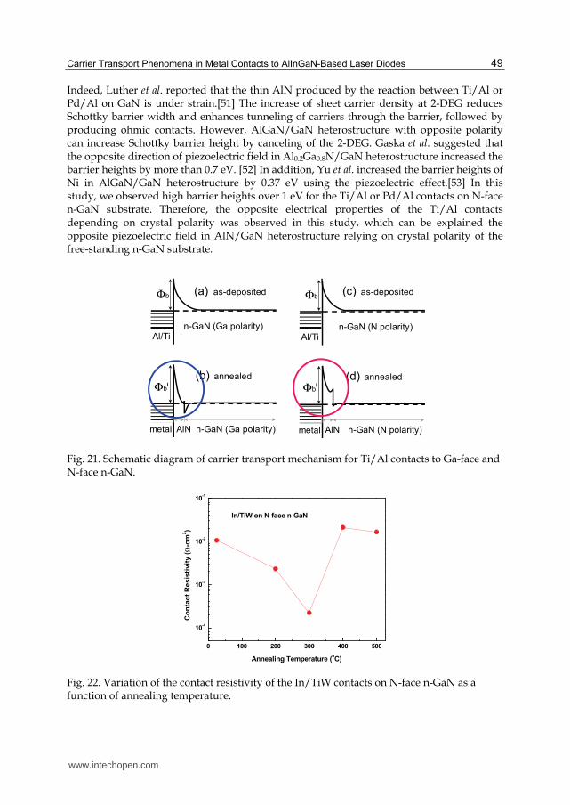
Luther et al. have characterized the interface of the Ti/Al and Pd/Al contacts on GaN, and a very thin layer of AlN has been observed at the interfaces of Ti/Al contact as well as Pd/Al contact annealed at 600 °C.[49] We also analyzed the Ti/Al on N-face n-GaN using field emission Auger electron spectroscopy, and found that Al peak was detected at the surface of GaN after annealing at 600 °C for 30 s.[50] As for the role of a thin AlN layer at the interface between Ti/Al or Pd/Al contacts and GaN, Luther et al. suggested that the formation of thin AlN layer (2-3 nm) could affect the band lineup between the metal contact and n-GaN by eliminating any Fermi level pinning at the metal/GaN interface, or could lower the barrier height, as is the case for other metal-insulator-semiconductor structures.[47,49] This suggestion can explain the formation of ohmic contact for the Ti/Al on Ga-face n-GaN substrate, meanwhile it cannot elucidate the production of Schottky contacts for the Ti/Al on N-face n-GaN observed in this study. Another possible explanation for the role of a thin AlN layer on the formation of the ohmic or Schottky contacts of Ti/Al depending on crystal polarity is production of opposite piezoelectric field at the AlN/GaN interface resulted from different polarity of GaN. Figure 21 shows the schematic diagrams of carrier transport mechanism for Ti/Al contacts to Ga-face and N-face n-GaN. Asbeck et al. reported that AlGaN/GaN heterostructure with Ga polarity increased the density of two-dimensional electron gas (2-DEG) by addition of the piezoelectrically-induced donor.[51] The addition of the piezoelectrically-induced donor occurs only in strained heterostructure with Ga polarity.
0.0 0.1 0.2 0.3 0.41x10⁻⁸
1x10⁻⁷
1x10⁻⁶
1x10⁻⁵
1x10⁻⁴
1x10⁻³
Ti/Al contacts on N-polar GaN wafer
Ti/Al, 500oC 30 s anneal
Ti/Al, 500oC 90 min anneal
Curr
en
t (A
)
Applied Voltage (V)
www.intechopen.com
Carrier Transport Phenomena in Metal Contacts to AlInGaN-Based Laser Diodes 49
Indeed, Luther et al. reported that the thin AlN produced by the reaction between Ti/Al or Pd/Al on GaN is under strain.[51] The increase of sheet carrier density at 2-DEG reduces Schottky barrier width and enhances tunneling of carriers through the barrier, followed by producing ohmic contacts. However, AlGaN/GaN heterostructure with opposite polarity can increase Schottky barrier height by canceling of the 2-DEG. Gaska et al. suggested that the opposite direction of piezoelectric field in Al0.2Ga0.8N/GaN heterostructure increased the barrier heights by more than 0.7 eV. [52] In addition, Yu et al. increased the barrier heights of Ni in AlGaN/GaN heterostructure by 0.37 eV using the piezoelectric effect.[53] In this study, we observed high barrier heights over 1 eV for the Ti/Al or Pd/Al contacts on N-face n-GaN substrate. Therefore, the opposite electrical properties of the Ti/Al contacts depending on crystal polarity was observed in this study, which can be explained the opposite piezoelectric field in AlN/GaN heterostructure relying on crystal polarity of the free-standing n-GaN substrate.
Fig. 21. Schematic diagram of carrier transport mechanism for Ti/Al contacts to Ga-face and N-face n-GaN.
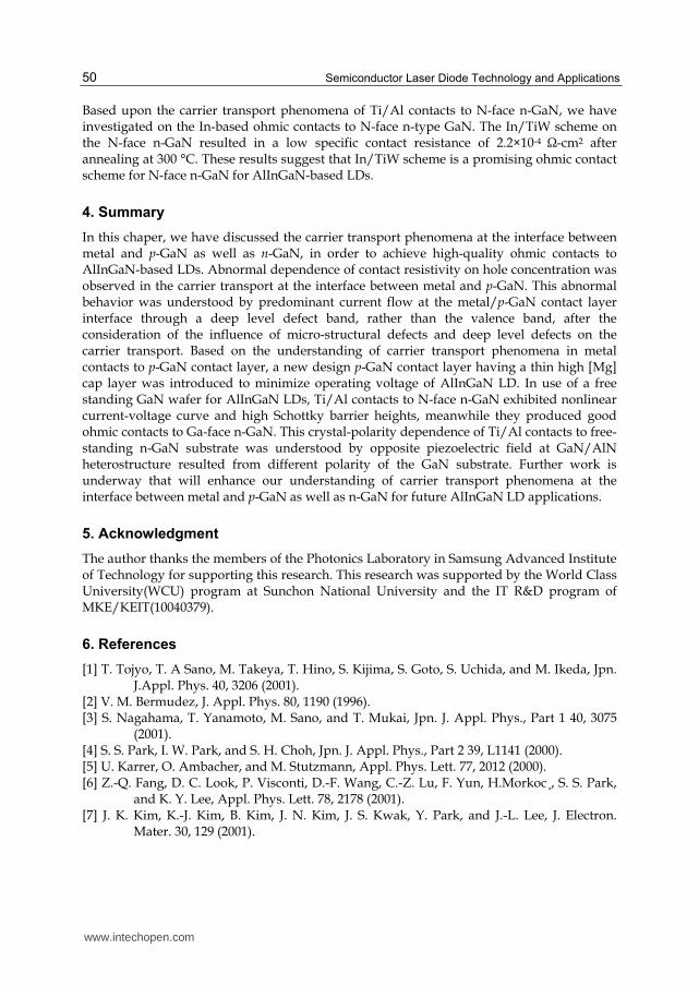
Fig. 22. Variation of the contact resistivity of the In/TiW contacts on N-face n-GaN as a function of annealing temperature.
n-GaN (Ga polarity)Al/Ti
Φb (a) as-deposited
(b) annealed
n-GaN (Ga polarity)metal
ΦbI
AlN
n-GaN (N polarity)Al/Ti
Φb(c) as-deposited
(d) annealed
n-GaN (N polarity)metal
ΦbI
AlN
0 100 200 300 400 500
10-4
10-3
10-2
10-1
Co
nta
ct
Re
sis
tivit
y (
Ω-c
m2)
Annealing Temperature (oC)
In/TiW on N-face n-GaN
www.intechopen.com
Semiconductor Laser Diode Technology and Applications 50
Based upon the carrier transport phenomena of Ti/Al contacts to N-face n-GaN, we have investigated on the In-based ohmic contacts to N-face n-type GaN. The In/TiW scheme on the N-face n-GaN resulted in a low specific contact resistance of 2.2×10⁻⁴ Ω-cm2 after annealing at 300 °C. These results suggest that In/TiW scheme is a promising ohmic contact scheme for N-face n-GaN for AlInGaN-based LDs.
4. Summary
In this chaper, we have discussed the carrier transport phenomena at the interface between metal and p-GaN as well as n-GaN, in order to achieve high-quality ohmic contacts to AlInGaN-based LDs. Abnormal dependence of contact resistivity on hole concentration was observed in the carrier transport at the interface between metal and p-GaN. This abnormal behavior was understood by predominant current flow at the metal/p-GaN contact layer interface through a deep level defect band, rather than the valence band, after the consideration of the influence of micro-structural defects and deep level defects on the carrier transport. Based on the understanding of carrier transport phenomena in metal contacts to p-GaN contact layer, a new design p-GaN contact layer having a thin high [Mg] cap layer was introduced to minimize operating voltage of AlInGaN LD. In use of a free standing GaN wafer for AlInGaN LDs, Ti/Al contacts to N-face n-GaN exhibited nonlinear current-voltage curve and high Schottky barrier heights, meanwhile they produced good ohmic contacts to Ga-face n-GaN. This crystal-polarity dependence of Ti/Al contacts to free-standing n-GaN substrate was understood by opposite piezoelectric field at GaN/AlN heterostructure resulted from different polarity of the GaN substrate. Further work is underway that will enhance our understanding of carrier transport phenomena at the interface between metal and p-GaN as well as n-GaN for future AlInGaN LD applications.
5. Acknowledgment
The author thanks the members of the Photonics Laboratory in Samsung Advanced Institute of Technology for supporting this research. This research was supported by the World Class University(WCU) program at Sunchon National University and the IT R&D program of MKE/KEIT(10040379).
6. References
[1] T. Tojyo, T. A Sano, M. Takeya, T. Hino, S. Kijima, S. Goto, S. Uchida, and M. Ikeda, Jpn. J.Appl. Phys. 40, 3206 (2001).
[2] V. M. Bermudez, J. Appl. Phys. 80, 1190 (1996). [3] S. Nagahama, T. Yanamoto, M. Sano, and T. Mukai, Jpn. J. Appl. Phys., Part 1 40, 3075
(2001). [4] S. S. Park, I. W. Park, and S. H. Choh, Jpn. J. Appl. Phys., Part 2 39, L1141 (2000). [5] U. Karrer, O. Ambacher, and M. Stutzmann, Appl. Phys. Lett. 77, 2012 (2000). [6] Z.-Q. Fang, D. C. Look, P. Visconti, D.-F. Wang, C.-Z. Lu, F. Yun, H.Morkoc¸, S. S. Park,
and K. Y. Lee, Appl. Phys. Lett. 78, 2178 (2001). [7] J. K. Kim, K.-J. Kim, B. Kim, J. N. Kim, J. S. Kwak, Y. Park, and J.-L. Lee, J. Electron.
Mater. 30, 129 (2001).
www.intechopen.com

Carrier Transport Phenomena in Metal Contacts to AlInGaN-Based Laser Diodes 51
[8] J. S. Kwak, J. Cho, S. Chae, O. H. Nam, C. Sone, and Y. Park, Jpn. J.Appl. Phys., Part 1 40, 6221 (2001).
[9] J.-S. Jang, S.-J. Park, and T.-Y. Seong, Appl. Phys. Lett. 76, 2898 (2000). [10] J. Ho, C. Jong, C. C. Chiu, C. Huang, C. Chen, and K. Shih, Appl. Phys. Lett. 74, 1275
(1999). [11] L. Zhou, W. Lanford, A. T. Ping, I. Adesida, J. W. Yang, and A. Khan, Appl. Phys. Lett.
76, 3451 (2000). [12] J.-S. Jang and T.-Y. Seong, Appl. Phys. Lett. 76, 2743 (2000). [13] L. T. Romano, M. Kneissl, J. E. Northrup, C. G. Van de Walle and D. W. Treat, Appl.
Phys. Lett. 79, 2734 (2001). [14] V. L. Rideout, Solid-State Electron. 18, 541 (1975). [15] S. M. Sze, Physics of Semiconductor Devices (Wiley, New York, 1981) pp. 245-311. [16] H. Morkoc, Nitride Semiconductors and Devices (Springer, Berlin, 1999), p. 155. [17] T. S. Zheleva, O. -H. Nam, M. D. Bremser, and R. F. Davis, Appl. Phys. Lett. 71, 2638
(1997). [18] A. Usui, H. Sunakawa, A. Sakai, and A. Yamaguchi, Jpn. J. Appl. Phys., Part 2 36, L899
(1997). [19] S. Nagahama, N. Iwasa, M. Senoh, T. Matsushita, Y. Sugimoto, H. Kiyoku, T. Kozaki, M.
Sano, H. Matsumura, H. Umemoto, K. Chocho, and T. Mukai, Jpn. J. Appl. Phys. 39, 647 (2000).
[20] T. Tojyo, T. Asano, M. Takeya, T. Hino, S. Goto, S. Uchida, and M. Ikeda, Jpn. J. Appl. Phys. 40, 3206 (2001).
[21] N. G. Weimann and L. F. Eastman, in Proceedings of the IEEE Cornell Conference, Cornell, NY, 1997.
[22] P. J. Hansen, Y. E. Strausser, A. N. Erickson, E. J. Tarse, P. Kozodoy, E. G. Brazel, J. P. Ibbetson, U. Mishra, V. Narayanamurti, S. P. DenBaars, and J. S. Speck, Appl. Phys. Lett. 72, 2247 (1998).
[23] P. Kozodoy, J. P. Ibbetson, H. Marchand, P. T. Fini, S. Keller, J. S. Speck, S. P. DenBaars, and U. K. Mishra, Appl. Phys. Lett. 73, 975 (1998).
[24] D. V. Kuksenkov, H. Temkin, A. Osinsky, R. Gaska, and M. A. Khan, Proceedings of the IEEE IEDM, 1997, p. 759.
[25] S. Tomiya, H. Nakajima, K. Funato, T. Miyajima, K. Kobayashi, T. Hino, S. Kijima, T. Asano, and M. Ikeda, Phys. Stat. Sol. (a) 188, 69 (2001)
[26] O. H. Nam, K. H. Ha, J. S. Kwak, S. N. Lee, K. K. Choi, T. H. Chang, S. H. Chae, W. S. Lee, Y. J. Sung, H. S. Paek, J. H. Chae, T. Sakong, and Y. Park, Phys. Stat. Sol. (c) 0, 2278 (2003).
[27] J. S. Kwak, O. H. Nam, and Y. Park, Appl. Phys. Lett. 80, 3554 (2002). [28] J. S. Kwak, O. H. Nam, and Y. Park, J. Appl. Phys. 95, 5917 (2004). [29] N. G. Weimann, L. F. Eastman, D. Doppalapudi, H. M. Ng, and T. D. Moustakas, J.
Appl. Phys. 38, 3656 (1998). [30] K. Shiojima, T. Suemitsu, and M. Ogura, Appl. Phys. Lett. 78, 3636 (2001). [31] S. J. Rosner, E. C. Carr, M. J. Ludowise, G. Girolami, and H. I. Erikson, Appl. Phys. Lett.
70, 420 (1997). [32] W. Götz, N. M. Johnson, and D. P. Bour, Appl. Phys. Lett. 68, 3470 (1996).
www.intechopen.com

Semiconductor Laser Diode Technology and Applications 52
[33] M.W. Bayerl, M. S. Brandt, O. Ambacher, M. Stutzmann, E. R. Glaser, R. L. Henry, A. E. Wickenden, D. D. Koleske, T. Suski, I. Grzegory, and S. Porowski, Phys. Rev. B 63, 125203 (2001).
[34] D. M. Hofmann, B. K. Meyer, H. Alves, F. Leiter, W. Burkhard, N. Romanov, Y. Kim, J. Krüger, and E. R. Weber, Phys. State. Sol. 180, 261 (2000).
[35] K. Shiojima, T. Sugahara, and S. Sakai, Appl. Phys. Lett. 77, 4353 (2000). [36] N. F. Mott, Phil. Mag. 19, 835 (1969). [37] D. C. Look, D. C. Walters, M. O. Manasreh, J. R. Sizelove, C. E. Stutz, and K. R. Evans,
Phys. Rev. B 42, 3578 (1990). [38] H. Yamamoto, Z-Q. Fang, and D. C. Look, Appl. Phys. Lett. 57, 1537 (1990). [39] T. Mori, T. Kozawa, T. Ohwaki, Y.Taga, S. Nagai, S. Yamasaki, S. Asami, N. Shibata, and
M. Koike, Appl. Phys. Lett. 69, 3537 (1996). [40] K. Shiojima, T. Sugahara, and S. Sakai, Appl. Phys. Lett. 77, 4353 (2000). [41] L. S. Yu, D. Qiao, L. Jia, S. S. Lau, Y. Qi, and K. M. Lau, Appl. Phys. Lett. 79, 4536 (2001). [42] M. G. Cheong, K. S. Kim, C. S. Kim, R. J. Choi, H. S. Yoon, N. W. Namgung, E. –K. Suh,
and J. L. Lee, Appl. Phys. Lett. 80, 1001 (2002). [43] J. S. Kwak, J. Cho, S. Chae, K. K. Choi, Y. J. Sung, S. N. Lee, O. H. Nam, and Y. Park,
Phys. Stat. Sol. (a) 194, 587 (2002). [44] J. S. Kwak, T. Jang, K. K. Choi, Y. J. Sung, Y. H. Kim, S. Chae, S. N. Lee, K. H. Ha, O. H.
Nam, and Y. Park, Phys. Stat. Sol. (a) 201, 2649 (2004). [45] S. Nagahama, T. Yanamoto, M. Sano, and T. Mukai, Jpn. J. Appl. Phys. 40, 3075 (2001). [46] S. S. Park, I. W. Park, and S. H. Choh, Jpn. J. Appl. Phys. 39, L1141 (2000). [47] B. P. Luther, S. E. Mohney, J. M. DeLucca, and R. F. Karlicek, Jr, J. Electron. Mater. 27,
196 (1998). [48] J. S. Kwak, S. E. Mohney, J. –Y. Lin, and R. S. Kern, Semicond. Sci. Technol. 15, 756
(2000). [49] B. P. Luther, J. M. DeLucca, S. E. Mohney, and R. F. Karlicek, Jr, Appl. Phys. Lett. 71,
3859 (1997). [50] J. S. Kwak, J. Cho and C. Sone, J. Kor. Phys. Soc. 48, 1259 (2006). [51] P. M. Asbeck, E. T. Yu, S. S. Lau, G. J. Sullivan, J. Van Hove, and J. Redwing, Electron.
Lett. 33, 1231 (1997). [52] R. Gaska, J. W. Yang, A. D. Bykhovski, M. S. Shur, V. V. Kaminski, and S. M. Soloviov,
Appl. Phys. Lett. 72, 64 (1998). [53] E. T. Yu, X. Z. Dang, L. S. Yu, D. Qiao, P. M. Asbeck, S. S. Lau, G. J. Sullivan, K. S.
Boutros, and J. Redwing, Appl. Phys. Lett. 73, 1880 (1998).
www.intechopen.com

Semiconductor Laser Diode Technology and ApplicationsEdited by Dr. Dnyaneshwar Shaligram Patil
ISBN 978-953-51-0549-7Hard cover, 376 pagesPublisher InTechPublished online 25, April, 2012Published in print edition April, 2012
InTech EuropeUniversity Campus STeP Ri Slavka Krautzeka 83/A 51000 Rijeka, Croatia Phone: +385 (51) 770 447 Fax: +385 (51) 686 166www.intechopen.com
InTech ChinaUnit 405, Office Block, Hotel Equatorial Shanghai No.65, Yan An Road (West), Shanghai, 200040, China
Phone: +86-21-62489820 Fax: +86-21-62489821
This book represents a unique collection of the latest developments in the rapidly developing world ofsemiconductor laser diode technology and applications. An international group of distinguished contributorshave covered particular aspects and the book includes optimization of semiconductor laser diode parametersfor fascinating applications. This collection of chapters will be of considerable interest to engineers, scientists,technologists and physicists working in research and development in the field of semiconductor laser diode, aswell as to young researchers who are at the beginning of their career.
How to referenceIn order to correctly reference this scholarly work, feel free to copy and paste the following:
Joon Seop Kwak (2012). Carrier Transport Phenomena in Metal Contacts to AlInGaN-Based Laser Diodes,Semiconductor Laser Diode Technology and Applications, Dr. Dnyaneshwar Shaligram Patil (Ed.), ISBN: 978-953-51-0549-7, InTech, Available from: http://www.intechopen.com/books/semiconductor-laser-diode-technology-and-applications/carrier-transport-phenomena-in-metal-contacts-to-alingan-based-laser-diodes

© 2012 The Author(s). Licensee IntechOpen. This is an open access articledistributed under the terms of the Creative Commons Attribution 3.0License, which permits unrestricted use, distribution, and reproduction inany medium, provided the original work is properly cited.