cathodoluminescence studies of electron injection effects
TRANSCRIPT
1
Cathodoluminescence Studies of Electron Injection Effects in Wide-Band-Gap
Semiconductors
Casey Schwarz, Leonid Chernyak and Elena Flitsiyan*
Physics Department, University of Central Florida, Orlando, FL, USA
1. Introduction
Recent developments in doping and growth of ZnO stimulated a renewal of interest in this material from the point of view of its applications in optoelectronic devices. As a direct wide bandgap semiconductor (Eg ≈ 3.35 eV at room temperature) with high exciton binding energy (60 meV, compared to 25 meV in GaN), ZnO is a superior candidate for minority-carrier-based devices, such as light emitting diodes, laser diodes, and transparent p-n junctions.
In the present state of the art, the development of the full potential of ZnO applications hinges in part on the availability of quality, highly conductive materials of both n- and p-type. Similar to GaN, achieving n-type conductivity in ZnO does not present a problem, since even nominally undoped material is generally n-type, due to the electrical activity of native defects, such as zinc interstitials, zinc antisites, and oxygen vacancies [1,2], as well as hydrogen impurities [3].
On the other hand, p-type conductivity with sufficiently high carrier concentrations appears to be much more elusive, mainly due to high ionization energies of potential acceptors, such as nitrogen, phosphorus, and arsenic. This problem is compounded by high concentrations of native and unintentional donors, which act as compensating centers, thus further reducing the free carrier concentration. It has been shown that the background donor concentration can be lowered if Mg is incorporated into the ZnO lattice, since each percent of Mg increases the bandgap of ZnO by 0.02 eV, suppressing the ionization of shallow donors [4]. The conversion to p-type can then be obtained by heavily doping the resultant material with phosphorus followed by annealing in O2 atmosphere [5].
Recently, successful p-type doping of ZnO also has been attained using phosphorus [6,7], nitrogen [8], arsenic [9], and antimony [10] yielding net hole concentrations up to 1018 cm-3. Even with the advent of new technology enabling the production of viable p-type materials, the performance of bipolar devices is fundamentally limited by the transport properties of minority carriers. In direct band gap semiconductors, including ZnO, minority carrier
*Corresponding author
www.intechopen.com
Cathodoluminescence
4
diffusion length is generally several orders of magnitude lower than in indirect gap materials such as silicon or germanium. In order to noticeably increase minority carrier diffusion length by reducing scattering by the dislocation walls, the edge threading dislocation density must be reduced by at least two orders of magnitude from a typical value of about 109 cm-2 in epitaxial ZnO layers [11-14].
Investigation of minority carrier diffusion lengths and lifetimes in both n- and p-type ZnO is an issue of practical importance, since it has direct implications on the performance of bipolar devices. Moreover, considering possible applications of these devices in high-temperature electronics, the insight into the temperature dependence of minority carrier properties is also of great value. Nonetheless, to the best of our knowledge, the reports on this subject are rather scarce. It is therefore the goal of this work to summarize the available information on the subject of minority carrier transport in ZnO and related compounds, focusing on its temperature dependence and the dynamics of non-equilibrium carrier recombination. This discussion will be preceded by a brief summary of the role of minority carrier transport in the performance of bipolar devices, as well as by the review of techniques of choice for measurement of the minority carrier diffusion length.
2. Role of minority carrier diffusion length in bipolar device performance
In general, when non-equilibrium carriers are generated in a material due to external excitation in the absence of an electric field, they diffuse over a certain distance before undergoing recombination. This parameter, namely the average distance traveled in a particular direction between generation and recombination, is characterized by the diffusion length, L. The diffusion length is related to the carrier lifetime, , (i.e., the time between generation and recombination of non-equilibrium carriers) through carrier diffusivity, D:
L D (1)
Diffusivity, or diffusion coefficient, is determined in turn by the mobility of the carriers, , according to the Einstein relation:
Bk TD
q (2)
where kB is the Boltzmann’s constant, T is absolute temperature, and q is the fundamental charge.
The diffusion process is driven by concentration gradients; since external excitation has a much larger impact on the concentration of minority carriers than that of majority ones (because generation density is usually much lower than the majority carrier density), it is the minority carriers that are more susceptible to diffusion. The electron diffusion current density is proportional to the gradient of the electron density, n, by the following relation;
n n
dnJ eD
dx (3)
www.intechopen.com
Cathodoluminescence Studies of Electron Injection Effects in Wide-Band-Gap Semiconductors
5
Where e is the charge of the electron and Dn is the electron diffusion coefficient. Relating the diffusion coefficient to temperature we get:
0 exp a
B
ED D
k T
(4)
With aE being the activation energy of the process. Using equation (1) we arrive at the equation relating the diffusion length to temperature by:
0 exp2
a
nB
EL L
k T (5)
CL peak intensity, ICL, of Near Band Edge (NBE) luminescence decays systematically with decreasing temperature. Since CL intensity is proportional to the rate of recombination, as the intensity decreases it is shown that the number of recombination events also decreases. Also, since the intensity is inversely proportional to the lifetime of carriers in the band, the decay of ICL indicates the increase of τ with temperature. This follows in an exponential relationship represented in this equation;
,1 exp
CLa T
B
AI
EB
k T
(6)
Where A and B are scaling factors, ΔEa,T is the thermal activation energy, kB is the Boltzmann constant and T is temperature.
Diffusion of minority carriers is a process that is fundamental to the operation of bipolar photovoltaic devices, with minority carrier diffusion length being the central parameter defining the device performance. In the presence of a p-n junction or a Schottky barrier, the non-equilibrium minority carriers generated by external excitation (e.g., light incident on a photodiode) within a few diffusion lengths of the space-charge region can be collected by the built-in field and thus contribute to the current flow across the device. The greater the diffusion length of the carriers, the more current can be collected, leading to the higher efficiency of the device. In photodiodes, it is usually only one side of the p-n junction that contributes to photocurrent. If the light is absorbed in the p-region of the junction, the quantum efficiency, , can be represented as follows:
exp( )
(1 ) 11 n
aWr
aL (7)
where r and a are the reflection and absorption coefficients, respectively, W is the width of the space-charge region, and Ln is the diffusion length of minority electrons.
Quantum efficiency is directly related to the spectral responsivity, R, of a photodiode:
( ) ph
op
I qR E
P E
(8)
www.intechopen.com
Cathodoluminescence
6
where Iph is total photocurrent, Pop is optical power incident on the device, q is the fundamental charge, and E is the energy of the incident photons. The relationship between minority carrier diffusion length and responsivity of Schottky photodiodes has been examined in great detail in Ref. [15]. Schottky photodiodes are among the simplest photovoltaic devices, where the non-equilibrium minority carriers, generated in the bulk of the semiconductor due to light absorption, are collected by the built-in field of the Schottky barrier deposited on the surface of the semiconductor. In order for the carriers to contribute to device current, they have to be generated within a few diffusion lengths of the collector.
For incident energies greater than the bandgap of the absorber material, non-equilibrium electron-hole pairs are generated only in the thin layer next to the surface of incidence, with the maximum depth of 1/aThis value is on the order of 100 nm in ZnO [16,17] and is generally much smaller than the thickness of the absorber layer. Considering a front-illuminated configuration (in which the incident light passes through the semitransparent Schottky contact), if L is greater than the generation depth, most of the non-equilibrium minority carriers are collected by the built-in field of the space-charge region. In this case, the internal quantum efficiency of the device approaches 100% and the responsivity is independent of the diffusion length value. Below this threshold, the responsivity decreases with L, provided that the width of the space-charge region is smaller than the generation depth.
If the energy of incident light is below the bandgap, light penetration depth is large (several micrometers), and a fair portion of the non-equilibrium carriers is generated in the neutral region of the semiconductor due to the ionization of the mid-gap levels. Since only the carriers within a few diffusion lengths of the space-charge region contribute to photocurrent, the responsivity at below-bandgap energies is limited by the diffusion length (unless the diffusion length exceeds the thickness of the absorber layer, in which case the latter is the limiting factor) [15].
3. Methods for determination of minority carrier lifetime and diffusion length
Although as of the date of this writing minority carrier transport in ZnO remains, with a few exceptions, essentially unexplored, however, the measurement of minority carrier diffusion length is a well-established subject. This section reviews three of the most widely used techniques, namely Electron Beam Induced Current (EBIC), Time-Resolved Photoluminescence (TRPL), and Time-Dependent Cathodoluminescence (CL) Measurements.
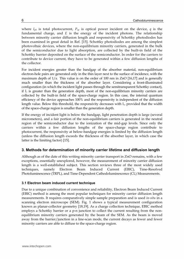
3.1 Electron beam induced current technique
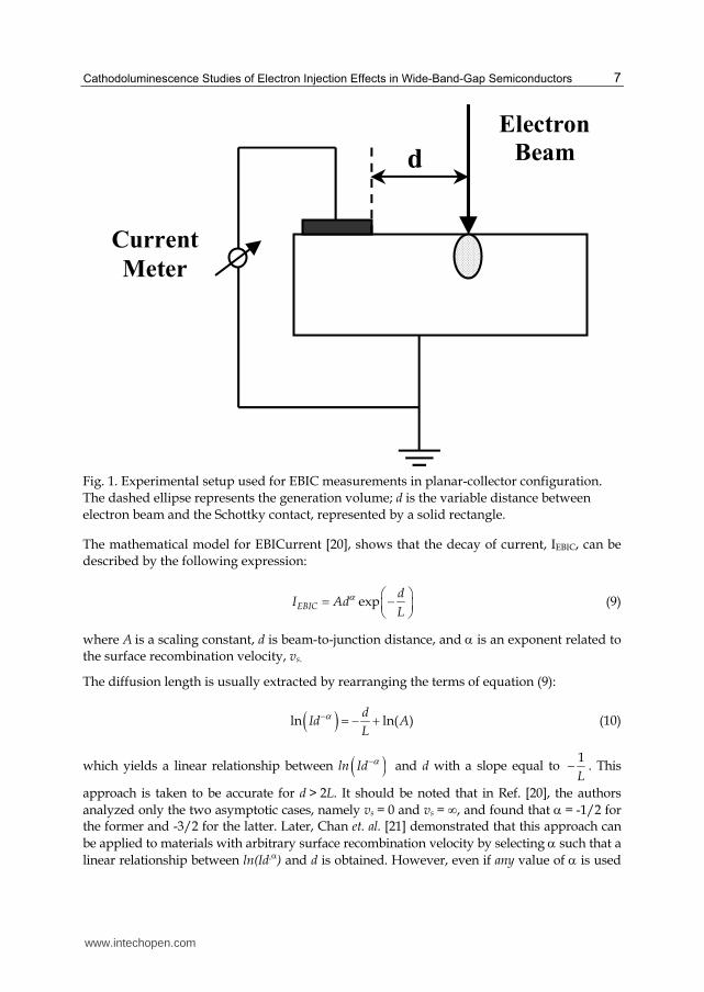
Due to a unique combination of convenience and reliability, Electron Beam Induced Current (EBIC) method is among the most popular techniques for minority carrier diffusion length measurements. It requires comparatively simple sample preparation and is used in-situ in a scanning electron microscope (SEM). Fig. 1 shows a typical measurement configuration known as planar-collector geometry [18,19]. As a charge collection technique, EBIC method employs a Schottky barrier or a p-n junction to collect the current resulting from the non-equilibrium minority carriers generated by the beam of the SEM. As the beam is moved away from the barrier/junction in a line-scan mode, the current decays as fewer and fewer minority carriers are able to diffuse to the space-charge region.
www.intechopen.com
Cathodoluminescence Studies of Electron Injection Effects in Wide-Band-Gap Semiconductors
7
d
Electron
Beam
Current
Meter
Fig. 1. Experimental setup used for EBIC measurements in planar-collector configuration. The dashed ellipse represents the generation volume; d is the variable distance between electron beam and the Schottky contact, represented by a solid rectangle.
The mathematical model for EBICurrent [20], shows that the decay of current, IEBIC, can be described by the following expression:
expEBIC
dI Ad
L (9)
where A is a scaling constant, d is beam-to-junction distance, and is an exponent related to the surface recombination velocity, vs.
The diffusion length is usually extracted by rearranging the terms of equation (9):
ln ln( )d
Id AL
(10)
which yields a linear relationship between ln Id and d with a slope equal to 1L
. This
approach is taken to be accurate for d > 2L. It should be noted that in Ref. [20], the authors analyzed only the two asymptotic cases, namely vs = 0 and vs = ∞, and found that = -1/2 for the former and -3/2 for the latter. Later, Chan et. al. [21] demonstrated that this approach can be applied to materials with arbitrary surface recombination velocity by selecting such that a linear relationship between ln(Id-) and d is obtained. However, even if any value of is used
www.intechopen.com
Cathodoluminescence
8
(such that -3/2 ≤ ≤-1/2), the result for the diffusion length changes by less than 20% [22] this is due to the fact that the exponential term dominating the value of IEBIC is independent of .
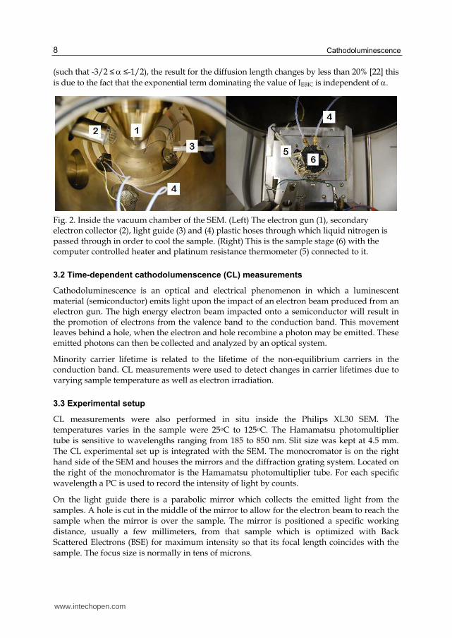
Fig. 2. Inside the vacuum chamber of the SEM. (Left) The electron gun (1), secondary electron collector (2), light guide (3) and (4) plastic hoses through which liquid nitrogen is passed through in order to cool the sample. (Right) This is the sample stage (6) with the computer controlled heater and platinum resistance thermometer (5) connected to it.
3.2 Time-dependent cathodolumenscence (CL) measurements
Cathodoluminescence is an optical and electrical phenomenon in which a luminescent material (semiconductor) emits light upon the impact of an electron beam produced from an electron gun. The high energy electron beam impacted onto a semiconductor will result in the promotion of electrons from the valence band to the conduction band. This movement leaves behind a hole, when the electron and hole recombine a photon may be emitted. These emitted photons can then be collected and analyzed by an optical system.
Minority carrier lifetime is related to the lifetime of the non-equilibrium carriers in the conduction band. CL measurements were used to detect changes in carrier lifetimes due to varying sample temperature as well as electron irradiation.
3.3 Experimental setup
CL measurements were also performed in situ inside the Philips XL30 SEM. The temperatures varies in the sample were 25oC to 125oC. The Hamamatsu photomultiplier tube is sensitive to wavelengths ranging from 185 to 850 nm. Slit size was kept at 4.5 mm. The CL experimental set up is integrated with the SEM. The monocromator is on the right hand side of the SEM and houses the mirrors and the diffraction grating system. Located on the right of the monochromator is the Hamamatsu photomultiplier tube. For each specific wavelength a PC is used to record the intensity of light by counts.
On the light guide there is a parabolic mirror which collects the emitted light from the samples. A hole is cut in the middle of the mirror to allow for the electron beam to reach the sample when the mirror is over the sample. The mirror is positioned a specific working distance, usually a few millimeters, from that sample which is optimized with Back Scattered Electrons (BSE) for maximum intensity so that its focal length coincides with the sample. The focus size is normally in tens of microns.
www.intechopen.com
Cathodoluminescence Studies of Electron Injection Effects in Wide-Band-Gap Semiconductors
9
The light collected from this focal point comes from a parallel beam through the hollow waveguide tube and focused onto the entrance slits of the monochromator. The electron beam may be used in spot or line scan mode. New areas are sampled after each temperature measurement is made to avoid contamination.
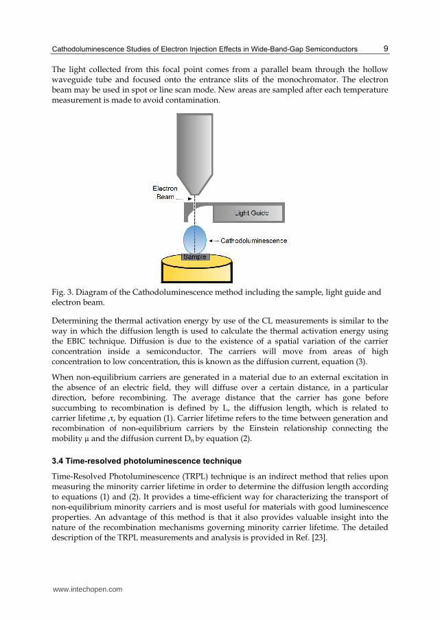
Fig. 3. Diagram of the Cathodoluminescence method including the sample, light guide and electron beam.
Determining the thermal activation energy by use of the CL measurements is similar to the way in which the diffusion length is used to calculate the thermal activation energy using the EBIC technique. Diffusion is due to the existence of a spatial variation of the carrier concentration inside a semiconductor. The carriers will move from areas of high concentration to low concentration, this is known as the diffusion current, equation (3).
When non-equilibrium carriers are generated in a material due to an external excitation in the absence of an electric field, they will diffuse over a certain distance, in a particular direction, before recombining. The average distance that the carrier has gone before succumbing to recombination is defined by L, the diffusion length, which is related to carrier lifetime ,τ, by equation (1). Carrier lifetime refers to the time between generation and recombination of non-equilibrium carriers by the Einstein relationship connecting the mobility µ and the diffusion current Dn by equation (2).
3.4 Time-resolved photoluminescence technique
Time-Resolved Photoluminescence (TRPL) technique is an indirect method that relies upon measuring the minority carrier lifetime in order to determine the diffusion length according to equations (1) and (2). It provides a time-efficient way for characterizing the transport of non-equilibrium minority carriers and is most useful for materials with good luminescence properties. An advantage of this method is that it also provides valuable insight into the nature of the recombination mechanisms governing minority carrier lifetime. The detailed description of the TRPL measurements and analysis is provided in Ref. [23].
www.intechopen.com
Cathodoluminescence
10
TRPL measurements are based on recording the transient decay of near-bandgap (NBE) photoluminescence excited by a short pulse of light, such as from a pulsed laser source. If the concentration of non-equilibrium minority carriers decreases exponentially from its initial value o, the intensity of the photoluminescence, IPL, also follows an exponential decay:
0 expPLR
tI
(11)
where R is the radiative recombination lifetime. In most cases, however, the photoluminescence intensity is affected not only by lifetime of minority carriers in the band, but also by the diffusion rate out of the absorber region, since the escape of the carriers from the active region is in this case equivalent to the reduction in their lifetime. Therefore, the lifetime obtained from the TRPL measurements is often less than the true minority carrier lifetime. In order to obtain an accurate measurement, it is necessary to introduce a confinement structure to reduce the influence of diffusion. In such a confinement structure the semiconductor of interest is “sandwiched” between two layers with wider bandgap and like doping type, so that the wide bandgap layers act as minority carrier mirrors.
4. Temperature dependence of minority carrier diffusion length and lifetime
4.1 Studies in n-type ZnO
Because of its intrinsic thermal stability, ZnO is a good candidate for high-temperature optoelectronic devices. However, the subject of the temperature dependence of minority carrier transport properties has not yet been adequately addressed in the literature. This section reviews the results obtained from variable-temperature diffusion length measurements performed on n-type ZnO [24].
The samples under investigation were weakly n-type ZnO substrates with electron concentration of ~ 1014 cm-3 and mobility of ~ 150 cm2/Vs. Secondary Ion Mass Spectroscopy (SIMS) measurements revealed the Li concentration of about 3x1016 cm-3 [25]. The Schottky contacts for EBIC measurements were deposited on the non-polar a-plane of ZnO crystal by electron beam evaporation of 80 nm-thick Au layer and subsequent lift-off. ZnO:N samples were grown using molecular beam epitaxy by SVT Associates. Hall effect measurements revealed hole concentration of 4.5x1017 cm-3 and mobility of ~1 cm2/V·s.
The studies of L as a function of temperature were carried out using EBIC method in a planar-collector configuration with a Schottky barrier (Sec. 3.1). At each temperature, several measurements were taken by scanning the beam of the SEM along a line perpendicular to the edge of the Schottky contact and recording the exponential decay of current. The recorded data were fitted with equation (9) using = -1/2. This value corresponds to zero surface recombination velocity which, given the excellent luminescence properties of this sample and a good fit to the experimental results, is a reasonably good approximation. It should be noted that each EBIC line-scan was recorded on a previously unexposed area in order to avoid the influence of electron irradiation on the value of diffusion length (cf. Sec. 5 below).
www.intechopen.com
Cathodoluminescence Studies of Electron Injection Effects in Wide-Band-Gap Semiconductors
11
Table 1 summarizes the results of EBIC measurements performed on one of the bulk ZnO samples and shows that the diffusion length of minority holes in n-ZnO increases with increasing temperature, T. The increase of L with T is not unique to this semiconductor. Similar trends were previously observed in GaAs [26] and later in GaN epitaxial layers [27]. In all cases, this increase was exponential with temperature and was modeled with the expression (5).
Temperature (oC) Diffusion Length (m) CL Intensity (103 counts)
25oC 0.438 ± 0.022 72.1 ± 3.7
50oC 0.472 ± 0.060 54.4 ± 3.8
75oC 0.493 ± 0.028 49.2 ± 2.4
100oC 0.520 ± 0.074 44.6 ± 4.7
125oC 0.547 ± 0.086 38.5 ± 6.8
EA (eV) 0.045 ± 0.002 0.058 ± 0.007
Table 1. Temperature dependence of minority carrier diffusion length and cathodoluminescence intensity of the near-band-edge peak in n-ZnO. After Ref. [24].
With the fit using equation (5), the experimental results for n-ZnO yields activation energy of 45 ± 2 meV [24]. This energy represents carrier de-localization energy, since it determines the increase of the diffusion length due to reduction of recombination efficiency [26]. The smaller is the activation energy, the more efficient is the de-trapping of captured carriers at a fixed temperature (see discussion below).
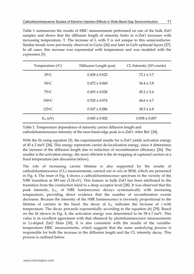
The role of increasing carrier lifetime is also supported by the results of cathodoluminescence (CL) measurements, carried out in-situ in SEM, which are presented in Fig. 4. The inset of Fig. 4 shows a cathodoluminescence spectrum in the vicinity of the NBE transition at 383 nm (3.24 eV). This feature in bulk ZnO has been attributed to the transition from the conduction band to a deep acceptor level [28]. It was observed that the peak intensity, ICL, of NBE luminescence decays systematically with increasing temperature, providing direct evidence that the number of recombination events decreases. Because the intensity of the NBE luminescence is inversely proportional to the lifetime of carriers in the band, the decay of ICL indicates the increase of with temperature. The decay proceeds exponentially according to the equation (6) [29]. Based on the fit shown in Fig. 4, the activation energy was determined to be 58 ± 7 meV. This value is in excellent agreement with that obtained by photoluminescence measurements in Li-doped ZnO films [30]. It is also consistent with the results of the variable-temperature EBIC measurements, which suggests that the same underlying process is responsible for both the increase in the diffusion length and the CL intensity decay. This process is outlined below.
www.intechopen.com
Cathodoluminescence
12
Fig. 4. Experimentally obtained values for the peak NBE CL intensity in ZnO:Li as a function of temperature (open circles) and the fit (solid line; equation (10)), yielding activation energy of 58 ± 7 meV. Inset: CL spectrum on n-ZnO showing the NBE transition at 25 oC. After Ref. [24].
The increase in minority hole lifetime in the valence band is likely associated with a smaller recombination capture cross-section for this carrier at elevated temperatures. In GaAs, for example, detailed analysis for temperature dependence of capture cross-section indicates an order of magnitude decrease of recombination efficiency, measured in terms of an “effective capture radius”, in the temperature range from 100 to 300 K [26]. Non-equilibrium electron-hole pairs are generated by the beam of the SEM and subsequently annihilate by recombining with each other. Since the hole capture cross-section is inversely proportional to temperature [26,31], the frequency of the recombination events (and, hence, the CL intensity) decreases as the temperature is raised. This means that non-equilibrium holes exist in the valence band for longer periods of time and, consequently, diffuse longer distances before undergoing recombination. Note that carrier diffusivity, D, is also a temperature-dependent quantity and, therefore, can affect the diffusion length (cf. equation (1)). On the other hand, it has been demonstrated for n-ZnO that the mobility, , of majority carriers decreases in the temperature range of our experiments by about a factor of 2 [32]. Assuming that the mobility of the minority carriers exhibits the same behavior [27] and combining equations (1) and (2), it is clear that the value of the diffusion length is dominated by the growing lifetime of minority holes. From the Einstein relation (equation (2)), the above-referenced difference in mobility translates to about a 30% decrease in diffusivity at 125 oC as compared to 25 oC. Based on a 30% difference in diffusivity and using experimentally obtained values of diffusion length, we conclude that the lifetime of minority holes at 125 oC is nearly 2.5 times greater than at room temperature.
www.intechopen.com
Cathodoluminescence Studies of Electron Injection Effects in Wide-Band-Gap Semiconductors
13
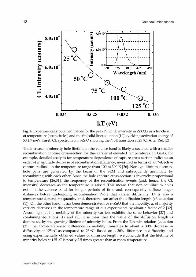
Preliminary results indicate that temperature-induced increase in carrier lifetime also occurs in epitaxial ZnO. Nitrogen-doped ZnO samples grown using molecular beam epitaxy were provided by SVT Associates. Hall effect measurements revealed hole concentration of 4.5x1017 cm-3 and mobility of ~1 cm2/V·s. Fig. 5 shows the decay of NBE CL intensity fitted with equation (6). The measurements yielded activation energy of 118 ± 12 meV. This value is comparable to the activation energy of the nitrogen acceptor in ZnO [34,35], which indicates possible non-equilibrium carrier trapping on nitrogen-related deep levels.
Fig. 5. Maximum CL intensity of the NBE transition in p-ZnO:N as a function of temperature (open circles). Solid line shows the fit with equation (10), resulting in activation energy of 118 ± 12 meV. After Ref. [33].
4.2 Studies in p-type ZnO doped with antimony
The possibility of p-type doping with larger radii atoms, such as antimony, has been explored in Refs. [10,36]. The studies demonstrated that despite the large size mismatch, which in principle should inhibit the substitution of this impurity on the oxygen site, effective p-type doping with hole concentrations up to 1020 cm-3 can be achieved [36]. These findings prompted the first-principles investigation by Limpijumnong et al., who suggested that the role of acceptors in size-mismatched impurity doped ZnO is performed by a complex of the impurity with two zinc vacancies SbZn-2VZn, the ionization energy of which is several-fold lower than that of a substitutional configuration and is consistent with the independent experimental observations [37]. Despite the encouraging predictions, however, very few attempts at achieving p-type conductivity in antimony-doped ZnO have been effective. Aoki et al. reported surprisingly high hole concentrations of up to 5 × 1020 cm-3 in ZnO:Sb films prepared by excimer laser doping [36]. Some of the authors also obtained p-type ZnO:Sb by molecular beam epitaxy (MBE) [10].
www.intechopen.com
Cathodoluminescence
14
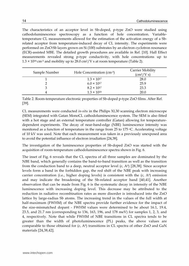
The characteristics of an acceptor level in Sb-doped, p-type ZnO were studied using cathodoluminescence spectroscopy as a function of hole concentration. Variable-temperature CL measurements allowed for the estimation of the activation energy of a Sb-related acceptor from temperature-induced decay of CL intensity. The experiments were performed on ZnO:Sb layers grown on Si (100) substrates by an electron cyclotron resonance (ECR)-assisted MBE. The detailed growth procedures are available in Ref. [10]. Hall Effect measurements revealed strong p-type conductivity, with hole concentrations up to 1.3 × 1018 cm-3 and mobility up to 28.0 cm2/V s at room temperature (Table 2).
Sample Number Hole Concentration (cm-3) Carrier Mobility
(cm2/V s) 1 1.3 × 10¹⁷ 28.0 2 6.0 × 10¹⁷ 25.9 3 8.2 × 10¹⁷ 23.3 4 1.3 × 10¹⁸ 20.0
Table 2. Room-temperature electronic properties of Sb-doped p-type ZnO films. After Ref. [39].
CL measurements were conducted in-situ in the Philips XL30 scanning electron microscope (SEM) integrated with Gatan MonoCL cathodoluminescence system. The SEM is also fitted with a hot stage and an external temperature controller (Gatan) allowing for temperature-dependent experiments. The decay of near-band-edge (NBE) luminescence intensity was monitored as a function of temperature in the range from 25 to 175 oC. Accelerating voltage of 10 kV was used. Note that each measurement was taken in a previously unexposed area to avoid the potential influence of electron irradiation [24,38].
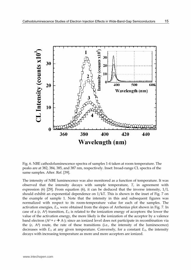
The investigation of the luminescence properties of Sb-doped ZnO was started with the acquisition of room-temperature cathodoluminescence spectra shown in Fig. 6.
The inset of Fig. 6 reveals that the CL spectra of all three samples are dominated by the NBE band, which generally contains the band-to-band transition as well as the transition from the conduction band to a deep, neutral acceptor level (e, A0) [28,38]. Since acceptor levels form a band in the forbidden gap, the red shift of the NBE peak with increasing carrier concentration (i.e., higher doping levels) is consistent with the (e, A0) emission and may indicate the broadening of the Sb-related acceptor band [40,41]. Another observation that can be made from Fig. 6 is the systematic decay in intensity of the NBE luminescence with increasing doping level. This decrease may be attributed to the reduction in radiative recombination rates as more disorder is introduced into the ZnO lattice by large-radius Sb atoms. The increasing trend in the values of the full width at half-maximum (FWHM) of the NBE spectra provide further evidence for the impact of the size-mismatched dopant - FWHM values were determined to be about 16.1, 19.4, 23.5, and 21.7 nm (corresponding to 136, 163, 196, and 178 meV) for samples 1, 2, 3, and 4, respectively. Note that while FWHM of NBE transitions in CL spectra tends to be greater than the width of photoluminescence (PL) peaks, the above values are comparable to those obtained for (e, A0) transitions in CL spectra of other ZnO and GaN materials [24,38,42].
www.intechopen.com
Cathodoluminescence Studies of Electron Injection Effects in Wide-Band-Gap Semiconductors
15
Fig. 6. NBE cathodoluminescence spectra of samples 1-4 taken at room temperature. The peaks are at 382, 384, 385, and 387 nm, respectively. Inset: broad-range CL spectra of the same samples. After. Ref. [39].
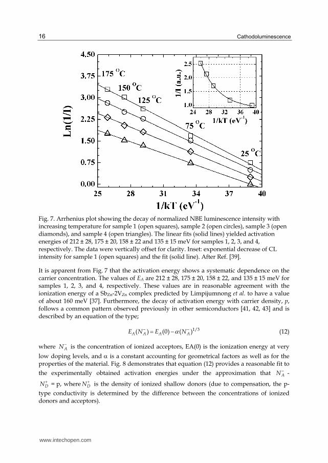
The intensity of NBE luminescence was also monitored as a function of temperature. It was observed that the intensity decays with sample temperature, T, in agreement with expression (6) [29]. From equation (6), it can be deduced that the inverse intensity, 1/I, should exhibit an exponential dependence on 1/kT. This is shown in the inset of Fig. 7 on the example of sample 1. Note that the intensity in this and subsequent figures was normalized with respect to its room-temperature value for each of the samples. The activation energies, EA, were obtained from the slopes of Arrhenius plot shown in Fig. 7. In case of a (e, A0) transition, EA is related to the ionization energy of acceptors: the lower the value of the activation energy, the more likely is the ionization of the acceptor by a valence band electron (A0 + e A-); since an ionized level does not participate in recombination via the (e, A0) route, the rate of these transitions (i.e., the intensity of the luminescence) decreases with EA at any given temperature. Conversely, for a constant EA, the intensity decays with increasing temperature as more and more acceptors are ionized.
www.intechopen.com
Cathodoluminescence
16
Fig. 7. Arrhenius plot showing the decay of normalized NBE luminescence intensity with increasing temperature for sample 1 (open squares), sample 2 (open circles), sample 3 (open diamonds), and sample 4 (open triangles). The linear fits (solid lines) yielded activation energies of 212 ± 28, 175 ± 20, 158 ± 22 and 135 ± 15 meV for samples 1, 2, 3, and 4, respectively. The data were vertically offset for clarity. Inset: exponential decrease of CL intensity for sample 1 (open squares) and the fit (solid line). After Ref. [39].
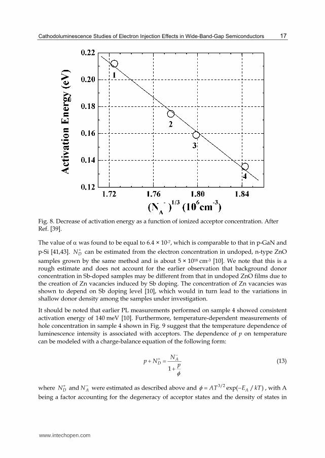
It is apparent from Fig. 7 that the activation energy shows a systematic dependence on the carrier concentration. The values of EA are 212 ± 28, 175 ± 20, 158 ± 22, and 135 ± 15 meV for samples 1, 2, 3, and 4, respectively. These values are in reasonable agreement with the ionization energy of a SbZn-2VZn complex predicted by Limpijumnong et al. to have a value of about 160 meV [37]. Furthermore, the decay of activation energy with carrier density, p, follows a common pattern observed previously in other semiconductors [41, 42, 43] and is described by an equation of the type;
1/3( ) (0) ( )A A A AE N E N (12)
where AN is the concentration of ionized acceptors, EA(0) is the ionization energy at very
low doping levels, and is a constant accounting for geometrical factors as well as for the properties of the material. Fig. 8 demonstrates that equation (12) provides a reasonable fit to the experimentally obtained activation energies under the approximation that AN -
DN = p, where DN is the density of ionized shallow donors (due to compensation, the p-type conductivity is determined by the difference between the concentrations of ionized donors and acceptors).
www.intechopen.com
Cathodoluminescence Studies of Electron Injection Effects in Wide-Band-Gap Semiconductors
17
Fig. 8. Decrease of activation energy as a function of ionized acceptor concentration. After Ref. [39].
The value of was found to be equal to 6.4 × 10⁻⁷, which is comparable to that in p-GaN and p-Si [41,43]. DN can be estimated from the electron concentration in undoped, n-type ZnO samples grown by the same method and is about 5 × 1018 cm-3 [10]. We note that this is a rough estimate and does not account for the earlier observation that background donor concentration in Sb-doped samples may be different from that in undoped ZnO films due to the creation of Zn vacancies induced by Sb doping. The concentration of Zn vacancies was shown to depend on Sb doping level [10], which would in turn lead to the variations in shallow donor density among the samples under investigation.
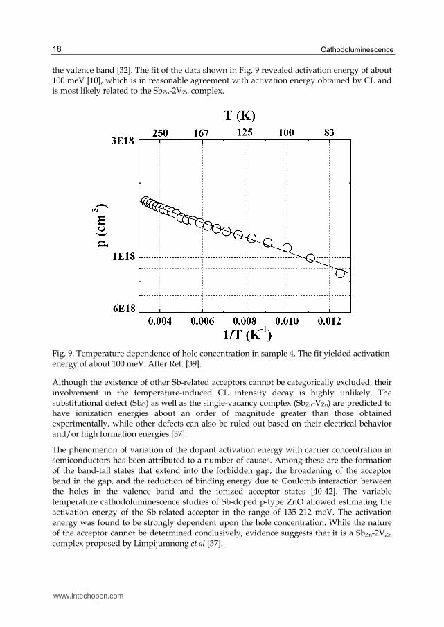
It should be noted that earlier PL measurements performed on sample 4 showed consistent activation energy of 140 meV [10]. Furthermore, temperature-dependent measurements of hole concentration in sample 4 shown in Fig. 9 suggest that the temperature dependence of luminescence intensity is associated with acceptors. The dependence of p on temperature can be modeled with a charge-balance equation of the following form:
1
AD
Np N
p
(13)
where DN and AN were estimated as described above and 3/2 exp( / )AAT E kT , with A being a factor accounting for the degeneracy of acceptor states and the density of states in
www.intechopen.com
Cathodoluminescence
18
the valence band [32]. The fit of the data shown in Fig. 9 revealed activation energy of about 100 meV [10], which is in reasonable agreement with activation energy obtained by CL and is most likely related to the SbZn-2VZn complex.
Fig. 9. Temperature dependence of hole concentration in sample 4. The fit yielded activation energy of about 100 meV. After Ref. [39].
Although the existence of other Sb-related acceptors cannot be categorically excluded, their involvement in the temperature-induced CL intensity decay is highly unlikely. The substitutional defect (SbO) as well as the single-vacancy complex (SbZn-VZn) are predicted to have ionization energies about an order of magnitude greater than those obtained experimentally, while other defects can also be ruled out based on their electrical behavior and/or high formation energies [37].
The phenomenon of variation of the dopant activation energy with carrier concentration in semiconductors has been attributed to a number of causes. Among these are the formation of the band-tail states that extend into the forbidden gap, the broadening of the acceptor band in the gap, and the reduction of binding energy due to Coulomb interaction between the holes in the valence band and the ionized acceptor states [40-42]. The variable temperature cathodoluminescence studies of Sb-doped p-type ZnO allowed estimating the activation energy of the Sb-related acceptor in the range of 135-212 meV. The activation energy was found to be strongly dependent upon the hole concentration. While the nature of the acceptor cannot be determined conclusively, evidence suggests that it is a SbZn-2VZn complex proposed by Limpijumnong et al [37].
www.intechopen.com
Cathodoluminescence Studies of Electron Injection Effects in Wide-Band-Gap Semiconductors
19
5. Studies of minority carrier recombination
Deep carrier traps have pronounced implications on minority carrier transport and often give rise to such undesirable phenomena as radiation-induced optical metastability, persistent photoconductivity and optical quenching of photocurrent [44-46]. On the other hand, it has been demonstrated that capture of minority carriers by deep metastable traps is associated with the increase of minority carrier diffusion length and lifetime [24,38,47]. Furthermore, in GaN this increase was shown to result in a significant (several-fold) improvement of photoresponse in agreement with equation (7) [22,47].
Extensive studies aimed at achieving p-type conductivity in ZnO reveal that most potential acceptors, such as nitrogen, phosphorus, and arsenic, tend to form acceptor levels far from the valence band maximum [48]. Since the ionization fraction of such acceptors is low (due to their high activation energy), there is a large concentration of neutral states that may act as traps for non-equilibrium electrons. The effects of electron trapping on the diffusion length and lifetime of minority carriers can be probed by subjecting the material of interest to the excitation by the electron beam of the scanning electron microscope. The remainder of this review deals with the influence of electron irradiation on minority carrier diffusion length (Sec. 5) and lifetime (Sec. 5.2).
5.1 Influence of electron trapping on minority carrier diffusion length
The measurements of diffusion length as a function of beam irradiation duration were carried out on bulk n-ZnO doped with lithium [24], molecular beam epitaxy (MBE) p-ZnO doped with nitrogen [49], phosphorus-doped ZnMgO grown by pulsed laser deposition (PLD) [38], and on Sb-doped epitaxial ZnO layers MBE grown on a Si substrate [39].
As was already mentioned, bulk ZnO samples (Tokyo Denpa Co.) were weakly n-type, showing electron concentrations of ~ 1014 cm-3 and mobility of ~ 150 cm2/Vs at room temperature. Secondary Ion Mass Spectroscopy (SIMS) measurements revealed the Li concentration of about 3x1016 cm-3 [25] (Li is often added to ZnO to increase the resistivity of initially n-type samples).
Phosphorus-doped Zn0.9Mg0.1O layers were fabricated using PLD. Capacitance-Voltage profiling of similar films, grown using the same procedure, resulted in net acceptor concentration of ~ 2x1018 cm-3 after annealing. Pt/Au (200/800 Å) layers were deposited on phosphorus-doped Zn0.9Mg0.1O films by electron beam evaporation and patterned by lift-off with contact diameters ranging from 50 to 375 m. Circular electrode pairs with significantly different surface areas were employed for the EBIC measurements. The electrodes create an asymmetric rectifying junction, based on back to back Schottky diodes, with the larger area electrode being pseudo-Ohmic.
EBIC experiments were conducted at room temperature in-situ in a Philips XL30 SEM using a planar-collector configuration with a Schottky barrier (Sec. 3.1) to monitor the changes in minority carrier diffusion length as a function of time. The results of EBIC experiments are presented in Fig. 10. Note that the results shown in the left panel of Fig. 10 and those discussed in Sec. 4 were obtained from different bulk ZnO samples, which may offer an explanation for the significant difference in the initial, room temperature values of diffusion length. Additionally, while the large diffusion length value of bulk ZnO can be attributed to
www.intechopen.com
Cathodoluminescence
20
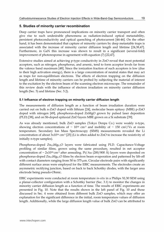
the higher quality of the bulk material (compared to the epitaxial layers), the diffusion length of ~ 2 µm in PLD-grown ZnMgO is rather surprising because of polycrystalline nature of the layers. It appears that in the latter sample, the transport of minority carriers is not significantly influenced by scattering from the grain boundaries.
Fig. 10. Experimental dependence of minority carrier diffusion length on duration of electron beam irradiation at room temperature (open circles) and the linear fit (solid line). After Refs. [24, 38, 49].
The experiments revealed that diffusion length follows a general trend in all samples studied. Fig. 10 shows that irradiation by the electron beam clearly results in a significant increase of the carrier diffusion length, and that this increase is linear with respect to the duration of electron irradiation (t). Up to 50% increase of diffusion length was achieved (cf. Fig. 10 (center)), with the rates of diffusion length increase ranging from ~13% to ~30% per 1000 s. This appears to be a common occurrence in wide bandgap semiconductors doped with species that create deep acceptor levels, as similar observations were made in (Al)GaN doped with Mg, Mn, Fe, and C [39,50,51]. It is also noteworthy that similar experiments conducted on bulk ZnO without any intentional dopants did no show any significant changes in minority carrier diffusion length [38].
The observed increase of L is ascribed to charging of the deep, neutral acceptor states by the electrons generated by the SEM beam, since trapping of non-equilibrium electrons prevents these levels from participating in recombination [38,39]. Therefore, the difference in the rates of diffusion length increase is likely explained, at least in part, by the difference in the concentrations of these deep centers [52].
EBIC measurements in Sb-doped ZnO were performed on the samples by moving the electron beam of the SEM from the edge of the Schottky barrier (created on the top surface of ZnO:Sb samples by Ti/Au evaporation followed by lift off) outwards (line-scan) and recording an exponential decay of induced current.
www.intechopen.com
Cathodoluminescence Studies of Electron Injection Effects in Wide-Band-Gap Semiconductors
21
After a single EBIC line-scan was completed (12 seconds), the excitation of the sample was continued by moving the electron beam back and forth along the same line for the total time of ~2200 seconds. EBIC measurements were periodically repeated to extract the minority carrier diffusion length [52], L, as a function of the duration of electron beam irradiation, t.
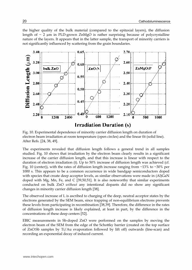
The effects of electron injection for Sb-doped 0.2 µm-thick p-type ZnO epitaxial layers (p = 1.3x1017 cm-3; µ = 28 cm2/Vs at room temperature) grown on Si substrate by MBE are summarized in Fig. 11. The activation energy for the e-beam injection-induced increase of L, EA,I = 219 ± 8 meV, was obtained from the graphs in Fig. 11b,c using the following equation:
, ,0 exp exp
2A I A TE E
R RkT kT
(14)
where R0 is a scaling constant, T is temperature, k is the Boltzmann’s constant, EA,I is the activation energy of electron irradiation effect, and EA,T is the activation energy of thermally-induced increase of L presented in Fig. 11a (EA,T = 184 ± 10 meV). The value of EA,I is in reasonable agreement with that for a SbZn-2VZn acceptor complex, predicted by Limpijumnong et al. [37] (see Ref. [53] for details).
Fig. 11. a) Diffusion length of minority electrons as a function of temperature (open circles) and the fit (solid line). Inset: Arrhenius plot of the same data yielding activation energy of 184 ± 10 meV. b) Electron beam irradiation-induced increase of minority electron diffusion length at different temperatures. The values of the diffusion length were vertically offset for clarity and are not intended to illustrate the temperature dependence. c) Rate of irradiation-induced increase of diffusion length as a function of temperature (open circles).The fit with equation 5 (solid line) gives activation energy of 219 ± 8 meV. After Ref. [53].
It can also be seen from Fig. 11 that the rate, R, of the diffusion length increase is reduced with increasing temperature. The increase of the diffusion length due to trapping is counteracted by the release of the trapped electrons that occurs if the carriers gain sufficient energy to escape the trap. As the temperature is raised, the likelihood of de-trapping increases, which dampens the irradiation-induced growth of the diffusion length.
www.intechopen.com
Cathodoluminescence
22
The saturation and relaxation of irradiation-induced change of diffusion length was studied at room temperature [53]. It was demonstrated that L reached its maximum value after about 50 min of continuous exposure to the electron beam. Further monitoring revealed that irradiation-induced increase persists for at least one week. Annealing the sample at 175 C for about 30 minutes resulted in a decrease of the diffusion length to about 1 µm. This behavior further supports the involvement of deep electron traps in the phenomenon of interest, since temperature-induced de- trapping of carriers (cf. Fig. 11,c) re-activates the original recombination route (cf. Fig. 11,a), thus reducing carrier lifetime and diffusion length.
5.2 Optical studies of the effects of electron trapping on minority carrier lifetime
According to equation (1), electron irradiation-induced increase in minority carrier diffusion length discussed above is associated with the increase of lifetime of non-equilibrium carriers. Experimental evidence for this dependence was obtained from the cathodoluminescence measurements performed on the same samples. Time-dependent CL measurements were conducted in-situ in SEM using setup described in section 3.2. This setup allows combining periodic acquisition of CL spectra with continuous excitation of the sample by scanning the beam over the same location. For temperature-dependent CL measurements, the sample temperature was varied in-situ using specially designed hot stage and an external temperature controller (Gatan). At each temperature, the electron beam irradiation and CL measurements were conducted at a different location.
5.2.1 Optical studies of Zn0.9Mg0.1O doped with phosphorus
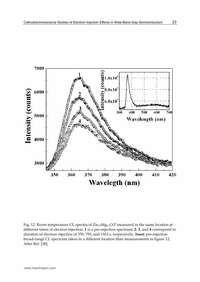
Fig. 12 shows a series of NBE transitions in p-type Zn0.9Mg0.1O:P recorded under continuous electron irradiation and numbered in order of increasing irradiation duration. The edge of this spectrum at ~ 355 nm (see also inset of Fig. 12) is in agreement with 10% Mg content in ZnO lattice, since each atomic percent of Mg is known to increase the ZnO band gap by 0.02 eV [4]. The observed CL spectrum is attributed to the band-to-band as well as band-to-impurity (P-acceptor) optical transitions. The inset of Fig. 12 shows a wider range spectrum featuring a broad band, which is likely defect related [54].
While no changes were observed in the broad band CL (cf. inset of Fig. 12), the near band-edge luminescence in Fig. 12 exhibits a continuous decay with increasing duration of electron beam irradiation. This demonstrates that exposure to the electron beam results in the increase of carrier lifetime (), since ICL is proportional to 1/. Similar phenomena were also observed in GaN, where the decay of NBE CL intensity occurred concomitantly with increasing diffusion length [38,50,51].
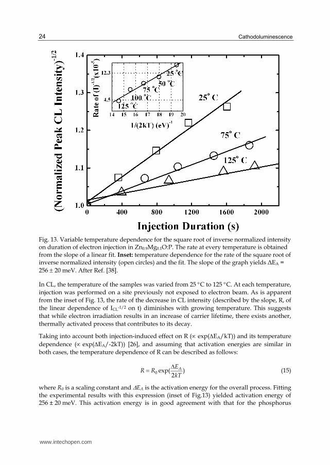
To characterize the intensity decay, we relate it to the diffusion length, L, which is known to vary linearly with duration of irradiation (cf. Fig. 13). Since L is proportional to 1/2 (equation (1)), the inverse square root of normalized (with respect to the initial maximum value) intensity must also be proportional to L, and consequently, would be expected to change linearly with duration of electron irradiation. Fig. 13 shows that this is indeed the case, indicating that the observed increase of the diffusion length is attributable to the growing lifetime of non-equilibrium carriers.
www.intechopen.com
Cathodoluminescence Studies of Electron Injection Effects in Wide-Band-Gap Semiconductors
23
Fig. 12. Room temperature CL spectra of Zn0.9Mg0.1O:P measured in the same location at different times of electron injection. 1 is a pre-injection spectrum; 2, 3, and 4 correspond to duration of electron injection of 359, 793, and 1163 s, respectively. Inset: pre-injection broad-range CL spectrum taken in a different location than measurements in figure 12. After Ref. [38].
www.intechopen.com
Cathodoluminescence
24
Fig. 13. Variable temperature dependence for the square root of inverse normalized intensity on duration of electron injection in Zn0.9Mg0.1O:P. The rate at every temperature is obtained from the slope of a linear fit. Inset: temperature dependence for the rate of the square root of inverse normalized intensity (open circles) and the fit. The slope of the graph yields ΔEA = 256 20 meV. After Ref. [38].
In CL, the temperature of the samples was varied from 25 C to 125 C. At each temperature, injection was performed on a site previously not exposed to electron beam. As is apparent from the inset of Fig. 13, the rate of the decrease in CL intensity (described by the slope, R, of the linear dependence of ICL-1/2 on t) diminishes with growing temperature. This suggests that while electron irradiation results in an increase of carrier lifetime, there exists another, thermally activated process that contributes to its decay.
Taking into account both injection-induced effect on R ( exp(EA/kT)) and its temperature dependence ( exp(EA/-2kT)) [26], and assuming that activation energies are similar in both cases, the temperature dependence of R can be described as follows:
0 exp( )2
AER R
kT
(15)
where R0 is a scaling constant and EA is the activation energy for the overall process. Fitting the experimental results with this expression (inset of Fig.13) yielded activation energy of 256 ± 20 meV. This activation energy is in good agreement with that for the phosphorus
www.intechopen.com
Cathodoluminescence Studies of Electron Injection Effects in Wide-Band-Gap Semiconductors
25
acceptor obtained based on the simple hydrogenic model. The model assumes phosphorus substitution on the oxygen site and predicts the activation energy of about 250-300 meV [55]. The experimentally obtained value of the activation energy, combined with the fact that no electron irradiation effects were observed in undoped ZnO [38], suggests that carrier trapping on phosphorus acceptor levels plays a crucial role in this phenomenon.
5.2.2 Optical studies of bulk ZnO
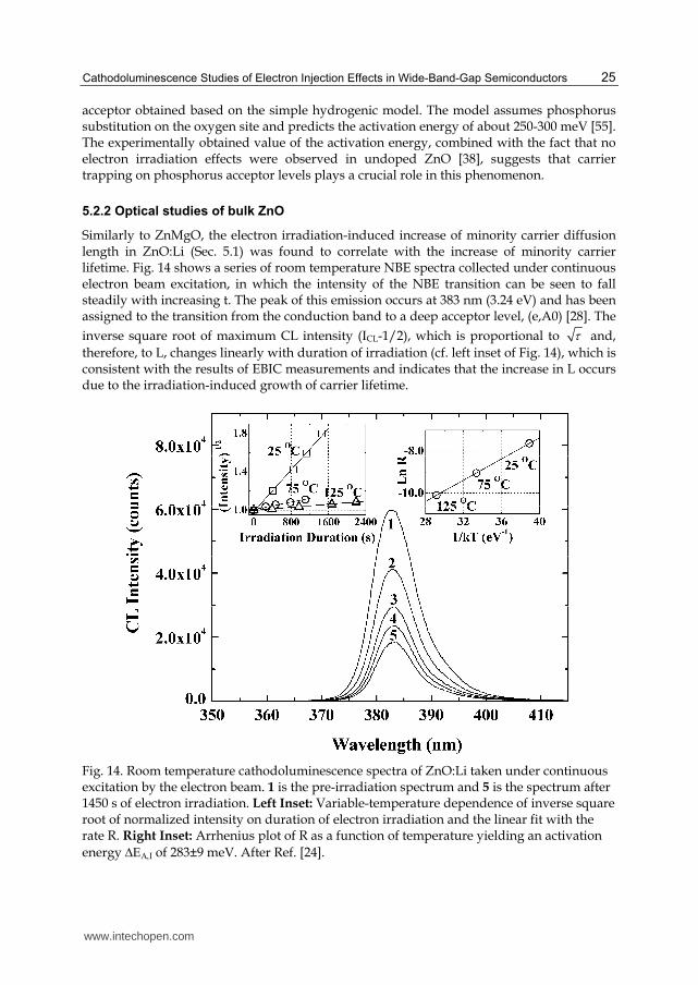
Similarly to ZnMgO, the electron irradiation-induced increase of minority carrier diffusion length in ZnO:Li (Sec. 5.1) was found to correlate with the increase of minority carrier lifetime. Fig. 14 shows a series of room temperature NBE spectra collected under continuous electron beam excitation, in which the intensity of the NBE transition can be seen to fall steadily with increasing t. The peak of this emission occurs at 383 nm (3.24 eV) and has been assigned to the transition from the conduction band to a deep acceptor level, (e,A0) [28]. The inverse square root of maximum CL intensity (ICL-1/2), which is proportional to and, therefore, to L, changes linearly with duration of irradiation (cf. left inset of Fig. 14), which is consistent with the results of EBIC measurements and indicates that the increase in L occurs due to the irradiation-induced growth of carrier lifetime.
Fig. 14. Room temperature cathodoluminescence spectra of ZnO:Li taken under continuous excitation by the electron beam. 1 is the pre-irradiation spectrum and 5 is the spectrum after 1450 s of electron irradiation. Left Inset: Variable-temperature dependence of inverse square root of normalized intensity on duration of electron irradiation and the linear fit with the rate R. Right Inset: Arrhenius plot of R as a function of temperature yielding an activation energy of 283±9 meV. After Ref. [24].
www.intechopen.com
Cathodoluminescence
26
CL measurements conducted at elevated temperatures confirmed the same trend for the irradiation-induced change of luminescence intensity. It can be seen from the left inset of Fig. 14 that the inverse square root of intensity increases linearly for all temperatures. The temperature dependence of rate, R, can be used to determine the activation energy of the irradiation-induced processes according to equation (15). On the other hand, our earlier studies of the temperature-induced CL intensity decay (Sec. 4) yielded the activation energy of about 60 meV [38], thus allowing us to separate the two components as followed from equation (14): the activation energy of electron irradiation effect ,A IE ; and, the previously determined, activation energy of thermally induced intensity decay ,A TE . This treatment yielded the value for ,A IE of 283 ± 9 meV. Incidentally, Ref. [25] also reports high concentration of ~0.3 eV electron traps found in the same material by Deep Level Transient Spectroscopy (DLTS). The significant difference between ,A IE and ,A TE observed in bulk ZnO suggests that, unlike in other materials, temperature- and irradiation-induced changes of the minority carrier transport characteristics are two distinctly different processes.
Although several theoretical works have predicted a very shallow LiZn level [56,57], these predictions have not been substantiated experimentally, as most studies find a rather deep Li-acceptor with activation energies of several hundred meVs [34,58]. In fact, recent first-principles calculations by Wardle et al., also suggest that the LiZn acceptor state lies at about 0.2 eV above the valence band maximum [58], which is in reasonable agreement with the
,A IE of 283 ± 9 meV obtained in this work.
It should be clarified that the weak n-type character of the sample is not necessarily in contradiction with the dominant behavior of acceptor states observed in electron trapping phenomena. As was mentioned, the n-type conductivity in nominally undoped ZnO is due to the shallow donor states, whereas in presence of deep electron traps the Fermi level may lie far below these states. Although shallow donors may capture non-equilibrium electrons under excitation, those are quickly released if the temperature is sufficiently high. Therefore, if the difference in the energetic position between the donor and trap states is large, the latter dominate the kinetics of electron trapping [59].
5.2.3 Optical studies of ZnO Doped with nitrogen
CL measurements performed on MBE-grown, nitrogen-doped p-ZnO revealed behavior similar to that of bulk ZnO [40] and PLD-grown ZnMgO [38]. Room temperature ZnO:N spectra are shown in Fig. 15 and feature a NBE luminescence band with a maximum at about 388 nm (~3.20 eV). This band includes the (e, A0) transition as well as the donor-acceptor pair (DAP) recombination, with nitrogen identified as the acceptor in both processes [60]. Additionally, a violet band centered on 435 nm has been attributed to the radiative recombination of the electrons trapped at grain boundaries with the holes in the valence band [61].
As expected, irradiation with electron beam resulted in decay of the intensity of NBE luminescence, indicating increasing lifetime. One can observe from the inset of Fig. 15 that, in agreement with the diffusion length measurements (cf. Fig. 10 in Sec. 5.1), the inverse square root of the peak normalized intensity of the NBE transition changes linearly with irradiation time, yielding the rate R. Note that the intensity of the violet band is not affected by electron irradiation, which suggests that electron trapping at the grain boundaries does not play a significant role in the irradiation-induced increase of carrier lifetime.
www.intechopen.com
Cathodoluminescence Studies of Electron Injection Effects in Wide-Band-Gap Semiconductors
27
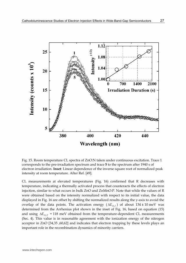
Fig. 15. Room temperature CL spectra of ZnO:N taken under continuous excitation. Trace 1 corresponds to the pre-irradiation spectrum and trace 5 to the spectrum after 1940 s of electron irradiation. Inset: Linear dependence of the inverse square root of normalized peak intensity at room temperature. After Ref. [49].
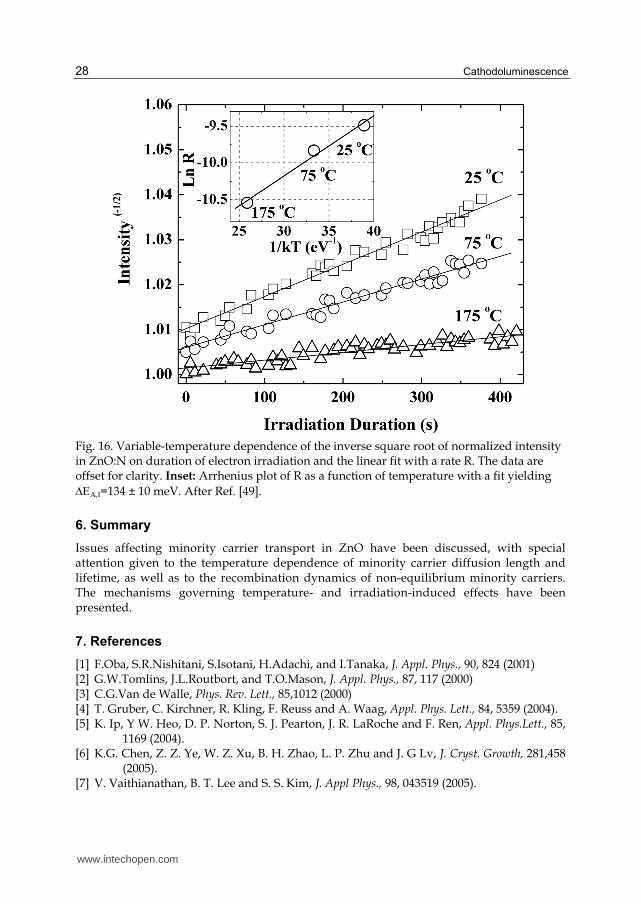
CL measurements at elevated temperatures (Fig. 16) confirmed that R decreases with temperature, indicating a thermally activated process that counteracts the effects of electron injection, similar to what occurs in bulk ZnO and ZnMnO:P. Note that while the values of R were obtained based on the intensity normalized with respect to its initial value, the data displayed in Fig. 16 are offset by shifting the normalized results along the y-axis to avoid the overlap of the data points. The activation energy ( ,A IE ) of about 134 ± 10 meV was determined from the Arrhenius plot shown in the inset of Fig. 16, based on equation (15) and using ,A TE = 118 meV obtained from the temperature-dependent CL measurements (Sec. 4). This value is in reasonable agreement with the ionization energy of the nitrogen acceptor in ZnO [34,35 ,60,62] and indicates that electron trapping by these levels plays an important role in the recombination dynamics of minority carriers.
www.intechopen.com
Cathodoluminescence
28
Fig. 16. Variable-temperature dependence of the inverse square root of normalized intensity in ZnO:N on duration of electron irradiation and the linear fit with a rate R. The data are offset for clarity. Inset: Arrhenius plot of R as a function of temperature with a fit yielding =134 ± 10 meV. After Ref. [49].
6. Summary
Issues affecting minority carrier transport in ZnO have been discussed, with special attention given to the temperature dependence of minority carrier diffusion length and lifetime, as well as to the recombination dynamics of non-equilibrium minority carriers. The mechanisms governing temperature- and irradiation-induced effects have been presented.
7. References
[1] F.Oba, S.R.Nishitani, S.Isotani, H.Adachi, and I.Tanaka, J. Appl. Phys., 90, 824 (2001) [2] G.W.Tomlins, J.L.Routbort, and T.O.Mason, J. Appl. Phys., 87, 117 (2000) [3] C.G.Van de Walle, Phys. Rev. Lett., 85,1012 (2000) [4] T. Gruber, C. Kirchner, R. Kling, F. Reuss and A. Waag, Appl. Phys. Lett., 84, 5359 (2004). [5] K. Ip, Y W. Heo, D. P. Norton, S. J. Pearton, J. R. LaRoche and F. Ren, Appl. Phys.Lett., 85,
1169 (2004). [6] K.G. Chen, Z. Z. Ye, W. Z. Xu, B. H. Zhao, L. P. Zhu and J. G Lv, J. Cryst. Growth, 281,458
(2005). [7] V. Vaithianathan, B. T. Lee and S. S. Kim, J. Appl Phys., 98, 043519 (2005).
www.intechopen.com
Cathodoluminescence Studies of Electron Injection Effects in Wide-Band-Gap Semiconductors
29
[8] E. J. Egerton, A. K. Sood, R. Singh, Y R. Puri, R. F. Davis, J. Pierce, D. C. Look, and T. Steiner, J. Electron. Mater., 34, 949 (2005).
[9] V. Vaithianathan, B. T. Lee, and S. S. Kim, Appl Phys. Lett., 86, 062101 (2005). [10] F. X. Xiu, Z. Yang, L. J. Mandalapu, D. T. Zhao, J. L. Liu, and W. P. Beyermann,
Appl.Phys. Lett., 87, 152101 (2005). [11] S. H. Lim, D. Shindo, H. B. Kang and K. Nakamura, J. Vac. Sci. Technol B, 19, 506 (2001). [12] K. Miyamoto, M. Sano, H. Kato and T. Yao, J. Cryst. Growth, 265, 34 (2004). [13] Y Wang, X. L. Du, Z. X. Mei, Z. Q. Zeng, Q. Y Xu, Q. K. Xue and Z. Zhang, J. Cryst.
Growth, 273, 100 (2004). [14] M. W. Cho, A. Setiawan, H. J. Ko, S. K. Hong and T. Yao, Semicond. Sci. Technol,20, S13
(2005). [15] E. Monroy, F. Calle, J. L. Pau, F. J. Sanchez, E. Munoz, F. Omnes, B. Beaumont, and P.
Gibart, J. Appl. Phys., 88, 2081 (2000). [16] J. F. Muth, R. M. Kolbas, A. K. Sharma, S. Oktyabrsky and J. Narayan, J. Appl. Phys.,85,
7884 (1999). [17] H. Yoshikawa and S. Adachi, Jpn. J. Appl. Phys. Part 1 - Regul. Pap. Short Notes Rev. Pap.,
36, 6237 (1997). [18] D. E. loannou and S. M. Davidson, J. Phys. D-Appl. Phys., 12, 1339 (1979). [19] D. E. loannou and C. A. Dimitriadis, IEEE Trans. Electron. Devices, 29, 445 (1982). [20] J. Boersma, J. J. E.Iindenkleef, and H. K. Kuiken, J. Eng. Math, 18, 315 (1984). [21] D. S. H. Chan, V. K. S. Ong, and J. C. H. Phang, IEEE Trans. Electron. Devices, 42, 963
(1995). [22] L. Chernyak, A. Osinsky and A. Schulte, Solid-State Electron., 45, 1687 (2001). [23] R. K. Ahrenkiel, Solid-State Electron., 35, 239 (1992). [24] O. Lopatiuk, L. Chernyak, A. Osinsky, J. Q. Xie, and P. P. Chow, Appl. Phys. Lett., 87,
214110 (2005) [25] A. Y. Polyakov, N. B. Smirnov, A. V. Govorkov, E. A. Kozhukhova, S. J. Pearton, D. P.
Norton, A. Osinsky, and A. Dabiran, J. Electron. Mater, 35, 663 (2006). [26] M. Eckstein and H. U. Habermeier, J. Phys. IV, 1, 23 (1991). [27] L. Chernyak, A. Osinsky, H. Temkin, J. W. Yang, Q. Chen and M. A. Khan, Appl Phys.
Lett., 69, 2531 (1996). [28] K. Thonke, T. Gruber, N. Teofilov, R. Schonfelder, A. Waag, and R. Sauer, Physica B,
308, 945 (2001). [29] D. S. Jiang, H. Jung and K. Ploog, J. Appl. Phys., 64, 1371 (1988). [30] A. Ortiz, C. Falcony, J. Hernandez, M. Garcia and J. C. Alonso, Thin Solid Films, 293, 103
(1997). [31] J. I. Pankove, Optical Processes in Semiconductors, Prentice-Hall, Englewood Cliffs, New
Jersey (1971). [32] D. C. Look, D. C. Reynolds, J. R. Sizelove, R. L. Jones, C. W. Litton, G. Cantwell and W.
C. Harsch, Solid State Commun., 105, 399 (1998). [33] O. Lopatiuk-Tirpak, “Influence of Electron Trapping on Minority Carrier Transport
Properties of Wide Band Gap Semiconductors”, Ph.D. Dissertation, University of Central Florida, Orlando, 2007.
[34] B. K. Meyer, H. Alves, D. M. Hofmann, W. Kriegseis, D. Forster, F. Bertram, J. Christen, A. Hoffmann, M. Strassburg, M. Dworzak, U. Haboeck, and A. V. Rodina, Phys. Status Solidi B - Basic Res., 241, 231 (2004).
www.intechopen.com
Cathodoluminescence
30
[35] S. Yamauchi, Y. Goto, and T. Hariu, J. Cryst. Growth, 260, 1 (2004). [36] T. Aoki, Y. Shimizu, A. Miyake, A. Nakamura, Y. Nakanishi and Y. Hatanaka, Phys.
Status Solidi B-Basic Res., 229, 911 (2002). [37] S. Limpijumnong, S. B. Zhang, S. H. Wei and C. H. Park, Phys. Rev. Lett., 92, 155504
(2004). [38] O. Lopatiuk, W. Burdett, L. Chernyak, K. P. Ip, Y. W. Heo, D. P. Norton, S. J. Pearton, B.
Hertog, P. P. Chow and A. Osinsky, Appl. Phys. Lett., 86, 012105 (2005). [39] O.Lopatiuk-Tirpak, W.V.Schoenfeld, L.Chernyak, F.X.Xiu, J.L.Liu, S.Jang, F.Ren,
S.J.Pearton, A.Osinsky, P.Chow, Appl. Phys. Lett., 88, 202110 (2006). [40] M. G. Cheong, K. S. Kim, C. S. Kim, R. J. Choi, H. S. Yoon, N. W. Namgung, E. K. Suh
and H. J. Lee, Appl. Phys. Lett., 80, 1001 (2002). [41] P. Kozodoy, H. L. Xing, S. P. DenBaars, U. K. Mishra, A. Saxler, R. Perrin, S. Elhamri
and W. C. Mitchel, J. Appl. Phys., 87, 1832 (2000). [42] W. Gotz, R. S. Kern, C. H. Chen, H. Liu, D. A. Steigerwald and R. M. Fletcher, Mater. Sci.
Eng. B-Solid State Mater. Adv. Technol., 59, 211 (1999). [43] P. P. Debye and E. M. Conwell, Phys. Rev., 93, 693 (1954). [44] S. Dhar and S. Ghosh, Appl. Phys. Lett., 80, 4519 (2002). [45] V. Ursaki, I. M. Tiginyanu, P. C. Ricci, A. Anedda, S. Hubbard and D. Pavlidis, J. Appl.
Phys., 94, 3875 (2003). [46] J. Ryan, D. P. Lowney, M. O. Henry, P. J. McNally, E. McGlynn, K. Jacobs and L.
Considine, Thin Solid Films, 473, 308 (2005). [47] L. Chernyak, G Nootz and A. Osinsky, Electron. Lett., 37, 922 (2001). [48] C. Look and B. Claftin, Phys. Status Solidi B - Basic Res., 241, 624 (2004). [49] O. Lopatiuk, A.Osinsky, L.Chernyak, in Zinc Oxide Bulk, Thin Films and Nanostructures,
pp.241-265, Edited by C. Jagadish and S. Pearton, Elsevier Ltd. (2006) [50] L. Chernyak, W. Burdett, M. Klimov and A. Osinsky, Appl. Phys. Lett., 82, 3680 (2003). [51] W. Burdett, O. Lopatiuk, L. Chernyak, M. Hermann, M. Stutzmann, and M. Eickhoff, J.
Appl. Phys., 96, 3556 (2004). [52] L. Chernyak, A. Osinsky, V. Fuflyigin and E. F. Schubert, Appl. Phys. Lett., 77, 875 (2000). [53] O.Lopatiuk-Tirpak, L.Chernyak, F.X.Xiu, J.L.Liu, S.Jang, F.Ren, S.J.Pearton,
K.Gartsman, Y.Feldman, A.Osinsky, P.Chow, J.Appl. Phys.,100, 086101 (2006). [54] Y. W. Heo, K. Ip, S. J. Pearton and D. P. Norton, Phys. Status Solidi A - Appl. Res., 201,
1500 (2004). [55] S. J. Pearton, D. P. Norton, K. Ip, Y. W. Heo and T. Steiner, Prog. Mater. Sci, 50, 293
(2005). [56] C. H. Park, S. B. Zhang and S. H. Wei, Phys. Rev. B, 66, 073202 (2002). [57] E. C. Lee and K. J. Chang, Phys. Rev. B, 70, 115210 (2004). [58] M. G. Wardle, J. P. Goss and P. R. Briddon, Phys. Rev. B, 71, 155205 (2005). [59] M. Salis, A. Anedda, F. Quarati, A. J. Blue and W. Cunningham, J. Appl. Phys., 97,
033709 (2005). [60] F. Reuss, C. Kirchner, T. Gruber, R. Kling, S. Maschek, W. Limmer, A. Waag, and P.
Ziemann, J. Appl. Phys., 95, 3385 (2004). [61] R. Ghosh, B. Mallik, S. Fujihara, and D. Basak, Chem. Phys. Lett., 403, 415 (2005). [62] G. Xiong, K. B. Ucer, R. T. Williams, J. Lee, D. Bhattacharyya, J. Metson, and P. Evans, J.
Appl. Phys., 97, 043528 (2005).
www.intechopen.com
CathodoluminescenceEdited by Dr. Naoki Yamamoto
ISBN 978-953-51-0362-2Hard cover, 324 pagesPublisher InTechPublished online 28, March, 2012Published in print edition March, 2012
InTech EuropeUniversity Campus STeP Ri Slavka Krautzeka 83/A 51000 Rijeka, Croatia Phone: +385 (51) 770 447 Fax: +385 (51) 686 166www.intechopen.com
InTech ChinaUnit 405, Office Block, Hotel Equatorial Shanghai No.65, Yan An Road (West), Shanghai, 200040, China
Phone: +86-21-62489820 Fax: +86-21-62489821
Cathodoluminescence (CL) is a non-destructive technique to characterize optical and electronic properties ofnanostructures in many kinds of materials. Major subject is to investigate basic parameters in semiconductors,impurities in oxides and phase determination of minerals. CL gives information on carrier concentration,diffusion length and life time of minority carriers in semiconductors, and impurity concentration and phasecomposition in composite materials. This book involves 13 chapters to present the basics in the CL techniqueand applications to particles, thin films and nanostructures in semiconductors, oxides and minerals. Thechapters covered in this book include recent development of CL technique and applications to wide range ofmaterials used in modern material science.
How to referenceIn order to correctly reference this scholarly work, feel free to copy and paste the following:
Casey Schwarz, Leonid Chernyak and Elena Flitsiyan (2012). Cathodoluminescence Studies of ElectronInjection Effects in Wide-Band-Gap Semiconductors, Cathodoluminescence, Dr. Naoki Yamamoto (Ed.), ISBN:978-953-51-0362-2, InTech, Available from:http://www.intechopen.com/books/cathodoluminescence/cathodoluminescence-studies-of-electron-injection-effects-in-wide-band-gap-semiconductors-

© 2012 The Author(s). Licensee IntechOpen. This is an open access articledistributed under the terms of the Creative Commons Attribution 3.0License, which permits unrestricted use, distribution, and reproduction inany medium, provided the original work is properly cited.