cbm2095 datasheet rev2.0
TRANSCRIPT

CBM2095 USB 2.0 Flash Disk Controller
Datasheet
Rev 2.0
Shenzhen Chipsbank Technologies Co.,Ltd. 7/F,Building No.12,Keji Central Road 2, Software Park, High-Tech Industrial Park, Shenzhen, P.R.China 518057 Tel: 0755-86169650-808 Fax: 0755-86169690 Email: [email protected]: http://www.chipsbank.com Contained herein Copyright by Shenzhen Chipsbank Technologies Co.,Ltd. all rights reserved.
CBM2095 Datasheet - 1 - 24/06/2010

Revision History
Date Rev No Description 2010-6-24 2.0 Initial release
CBM2095 Datasheet - 2 - 24/06/2010
Contents
1 DESCRIPTION ........................................................................................................................................ 4
2 FEATURES .............................................................................................................................................. 4
3 BLOCK DIAGRAM ................................................................................................................................. 6
4 PIN ASSIGNMENT ................................................................................................................................. 7
4.1 TQFP48 (TOP SIDE) ....................................................................................................................................... 7
5 PIN DESCRIPTION ................................................................................................................................ 8
6 ELECTRICAL CHARACTERISTICS ..................................................................................................11
6.1 ABSOLUTE MAXIMUM RATINGS .................................................................................................................... 11 6.2 RECOMMENDED OPERATING CONDITIONS..................................................................................................... 11 6.3 STATIC CHARACTERISTICS ............................................................................................................................ 12 6.4 DYNAMIC CHARACTERISTICS ....................................................................................................................... 12
6.4.1 Normal NAND FLASH Dynamic characteristics .................................................................................... 12 6.4.2 ONFI NAND FLASH Dynamic characteristics ....................................................................................... 14 6.4.3 TOGGLE NAND FLASH Dynamic characteristics................................................................................. 19
7 MECHANICAL DIMENSIONS ............................................................................................................ 24
7.1 48-PIN CBM2095 PACKAGE OUTLINE DIMENSION ...................................................................................... 24
8 COPYRIGHT NOTICE ......................................................................................................................... 25
CBM2095 Datasheet - 3 - 24/06/2010

1 Description
Fastest & Securest USB 2.0 Flash Disk Controller with dedicated 32-bit microprocessor
The CBM2095 is the USB 2.0 Flash Disk controller with the fastest transfer speed on the market. CBM2095 can reach theoretical flash access speed limit of over 32MByte/s for read and 20MByte/s for write.
The on-the-fly ECC engine is capable of correcting up to 16/25/29/30bits per 1024 bytes page . For data security, CBM2095 is designed with both hardware and software data protection technology to prevent data corruption even if it is powered off or unplugged during data transfer.
The CBM2095 supports all 8 /16 bit BUS wide async NAND flash memory available in the market. New flash can be supported by software re-configuration.
The CBM2095 supports all 8 bit BUS wide ONFI/TOGGLE NAND flash memory available in the market. New flash can be supported by software re-configuration.
The CBM2095 has both a) 5V to 3.3V LDO and b) power on reset circuits integrated. Thus greatly reduced BOM cost and eased layout burden.
The CBM2095 can work properly with no external crystal. It was popularly used for UDP products.
The CBM2095 runs smoothly with all available hosts and PC platforms. Complied with USB specification rev. 2.0, the CBM2095 can be supported without additional driver under Win XP, Win 2000, Windows Me, Mac OS and Linux OS. With device driver installed, it can support Win 98/98SE as well. Comprehensive applications, such as PC boot up, disk partitions, password check for security disk, are available as part of our standard mass production software package.
The CBM2095 is available in 48-pin TQFP and 64-pin LQFP package, which are thinnest and smallest on the market. The 48-pin CBM2095 supports up to 4 flash chips and the 64-pin CBM2095 supports up to 8 flash chips. Customers can choose different packages to meet their design requirement.
2 Features
USB Interface
High-speed USB 2.0 interface;
Fastest data transfer rate on the market
Dual-channel mode: 32MB/s for Read, 20MB/s for Write Single-channel mode: 26MB/s for Read, 20MB/s for Write
Fastest file copy rate on the market.
On-the-fly ECC built-in Hardware enhances reliability
ECC for NAND flash: 16/25/29/30 bit per page (1 page = 1024 bytes)
Special wear leveling algorithm to improve the flash life-time
Hardware & Software Data Protection Technology
CBM2095 Datasheet - 4 - 24/06/2010
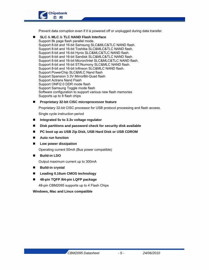
Prevent data corruption even if it is powered off or unplugged during data transfer.
SLC & MLC & TLC NAND Flash Interface Support 8k page flash parallel mode. Support 8-bit and 16-bit Samsung SLC&MLC&TLC NAND flash. Support 8-bit and 16-bit Toshiba SLC&MLC&TLC NAND flash. Support 8-bit and 16-bit Hynix SLC&MLC&TLC NAND flash. Support 8-bit and 16-bit Sandisk SLC&MLC&TLC NAND flash. Support 8-bit and 16-bit Micron/Intel SLC&MLC&TLC NAND flash. Support 8-bit and 16-bit ST/Numony SLC&MLC NAND flash. Support 8-bit and 16-bit Infineon SLC&MLC NAND flash. Support PowerChip SLC&MLC Nand flash Support Spansion 3.3V MirrorBit-Quad flash Support Actrans Nand Flash Support ONFI2.0 DDR mode flash Support Samsung Toggle mode flash Software configuration to support various new flash memories Supports up to 8 flash chips
Proprietary 32-bit CISC microprocessor feature
Proprietary 32-bit CISC processor for USB protocol processing and flash access.
Single cycle instruction period
Integrated 5v to 3.3v voltage regulator
Disk partitions and password check for security disk available
PC boot up as USB Zip Disk, USB Hard Disk or USB CDROM
Auto run function
Low power dissipation
Operating current 50mA (Bus power compatible)
Build-in LDO
Output maximum current up to 300mA
Build-in crystal
Leading 0.16um CMOS technology
48-pin TQFP /64-pin LQFP package
48-pin CBM2095 supports up to 4 Flash Chips
Windows, Mac and Linux compatible
CBM2095 Datasheet - 5 - 24/06/2010

3 Block Diagram
CBM2095 Datasheet - 6 - 24/06/2010
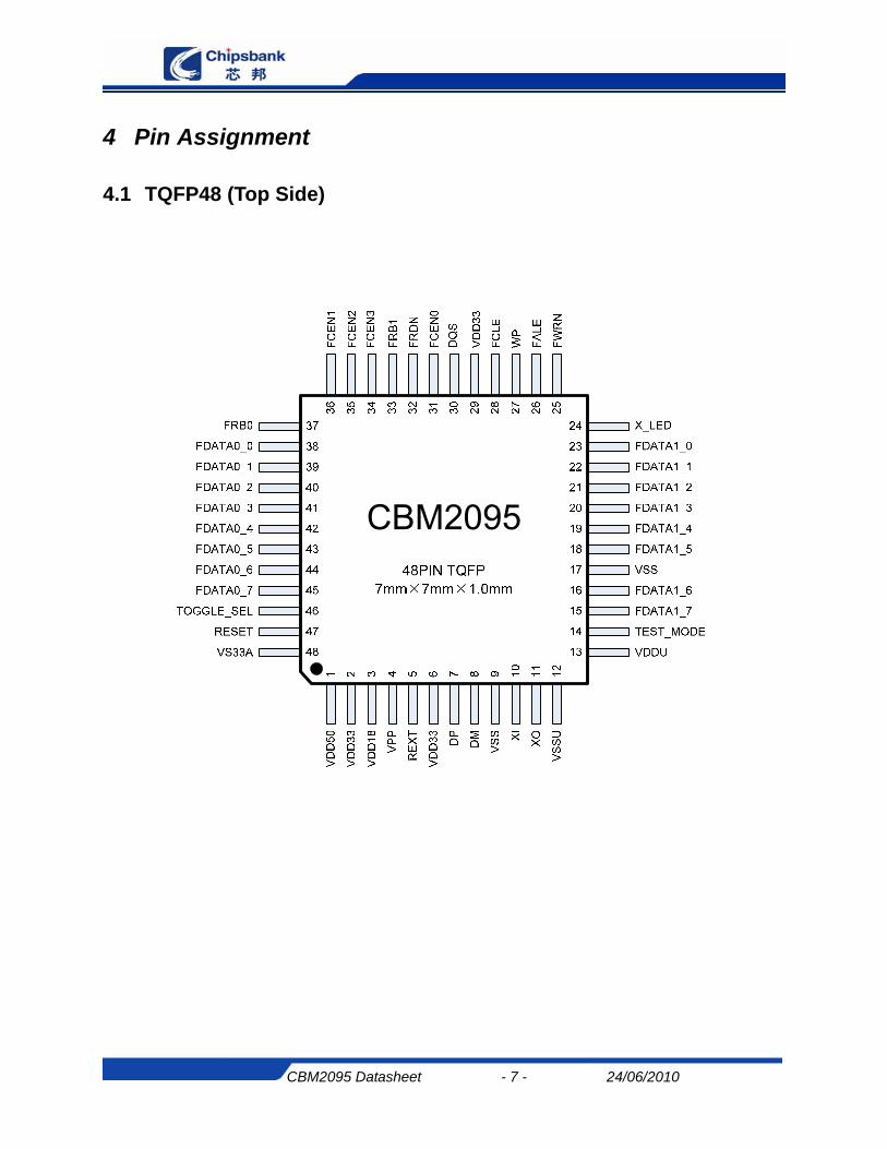
4 Pin Assignment
4.1 TQFP48 (Top Side)
CBM2095 Datasheet - 7 - 24/06/2010
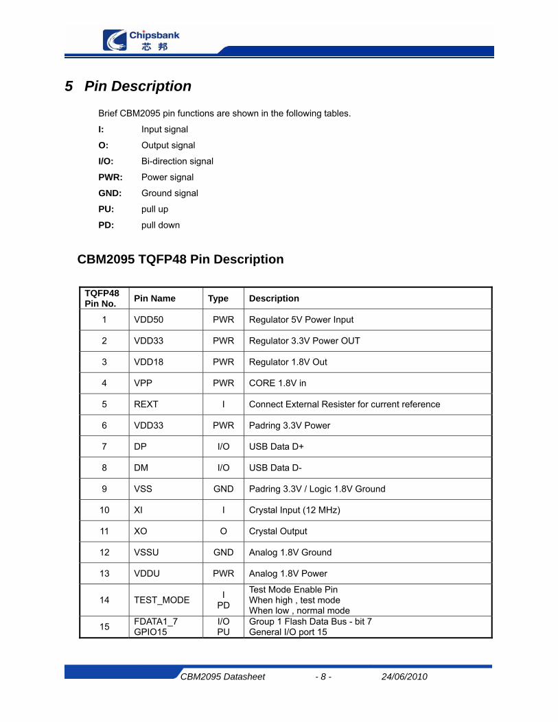
5 Pin Description
Brief CBM2095 pin functions are shown in the following tables.
I: Input signal
O: Output signal
I/O: Bi-direction signal
PWR: Power signal
GND: Ground signal
PU: pull up
PD: pull down
CBM2095 TQFP48 Pin Description
TQFP48 Pin No. Pin Name Type Description
1 VDD50 PWR Regulator 5V Power Input
2 VDD33 PWR Regulator 3.3V Power OUT
3 VDD18 PWR Regulator 1.8V Out
4 VPP PWR CORE 1.8V in
5 REXT I Connect External Resister for current reference
6 VDD33 PWR Padring 3.3V Power
7 DP I/O USB Data D+
8 DM I/O USB Data D-
9 VSS GND Padring 3.3V / Logic 1.8V Ground
10 XI I Crystal Input (12 MHz)
11 XO O Crystal Output
12 VSSU GND Analog 1.8V Ground
13 VDDU PWR Analog 1.8V Power
14 TEST_MODE I PD
Test Mode Enable Pin When high , test mode When low , normal mode
15 FDATA1_7 GPIO15
I/O PU
Group 1 Flash Data Bus - bit 7 General I/O port 15
CBM2095 Datasheet - 8 - 24/06/2010

When select spi mode ,as spi chip select . (configure as GPIO and clear pin_64( detail in spi_ctl[13] .when select master mode , configure output , otherwise, configure as input.).
16 FDATA1_6 GPIO14
I/O PU
Group 1 Flash Data Bus - bit 6 General I/O port 14 When select spi mode, as clock out support ligh-tun sensor (configure as GPIO and clear pin_64( detail in spi_ctl[13] .when select ligh-tun mode , configure output).
17 VSS GND Padring 3.3V / Logic 1.8V Ground
18 FDATA1_5 GPIO13
I/O PU
Group 1 Flash Data Bus - bit 5 General I/O port 13
19 FDATA1_4 GPIO12
I/O PU
Group 1 Flash Data Bus - bit 4 General I/O port 12
20 FDATA1_3 GPIO11
I/O PU
Group 1 Flash Data Bus - bit 3 General I/O port 11
21 FDATA1_2 GPIO10
I/O PU
Group 1 Flash Data Bus - bit 2 General I/O port 10
22 FDATA1_1 GPIO9
I/O PU
Group 1 Flash Data Bus - bit 1 General I/O port 9
23 FDATA1_0 GPIO8
I/O PU
Group 1 Flash Data Bus - bit 0 General I/O port 8
24 X_LED I/O When TEST_MODE =1, as scan clock input. When TEST_MODE =0, as LED Indication
25 FWRN O Group Flash Write Enable (active low)
26 FALE O Group Flash Address Latch Enable
27 WP I Write Protect Switch Input
28 FCLE O Group Flash Command Latch Enable
29 VDD33 PWR Padring 3.3V Power
30 DQS I/O PD DQS, only for onfi/toggle nand flash
31 FCEN0 O Flash Chip Enable - Chip 0 (active low)
32 FRDN O Group Flash Read Enable (active low)
33 FRB1 /INTR I
Group Flash Ready_Busy 1, when select flash_rb1 mode, as Group Flash Ready_Busy1 signal input(detail in soft_flag [25]). 2, when select intr mode, as external interrupt input signal(detail in soft_flag [25]).
34 /SCK(I2c) FCEN3 O
1, When select test-mode, as scan-chain output 2, When select i2c , as sck 3, When select chip select2/3 mode, as CE3 output
35 FCEN2
I/O PU
1, When select test_mode, As scan-chain input 2, when select chip select2/3 mode, as CE2 output .(active when disable test_mode)
CBM2095 Datasheet - 9 - 24/06/2010
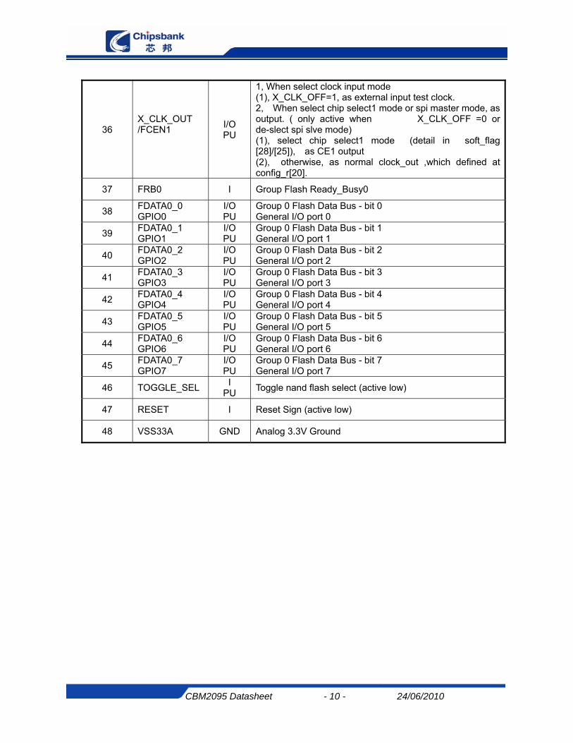
36 X_CLK_OUT /FCEN1
I/O PU
1, When select clock input mode (1), X_CLK_OFF=1, as external input test clock. 2, When select chip select1 mode or spi master mode, as output. ( only active when X_CLK_OFF =0 or de-slect spi slve mode) (1), select chip select1 mode (detail in soft_flag [28]/[25]), as CE1 output (2), otherwise, as normal clock_out ,which defined at config_r[20].
37 FRB0 I Group Flash Ready_Busy0
38 FDATA0_0 GPIO0
I/O PU
Group 0 Flash Data Bus - bit 0 General I/O port 0
39 FDATA0_1 GPIO1
I/O PU
Group 0 Flash Data Bus - bit 1 General I/O port 1
40 FDATA0_2 GPIO2
I/O PU
Group 0 Flash Data Bus - bit 2 General I/O port 2
41 FDATA0_3 GPIO3
I/O PU
Group 0 Flash Data Bus - bit 3 General I/O port 3
42 FDATA0_4 GPIO4
I/O PU
Group 0 Flash Data Bus - bit 4 General I/O port 4
43 FDATA0_5 GPIO5
I/O PU
Group 0 Flash Data Bus - bit 5 General I/O port 5
44 FDATA0_6 GPIO6
I/O PU
Group 0 Flash Data Bus - bit 6 General I/O port 6
45 FDATA0_7 GPIO7
I/O PU
Group 0 Flash Data Bus - bit 7 General I/O port 7
46 TOGGLE_SEL I PU Toggle nand flash select (active low)
47 RESET I Reset Sign (active low)
48 VSS33A GND Analog 3.3V Ground
CBM2095 Datasheet - 10 - 24/06/2010
6 Electrical Characteristics
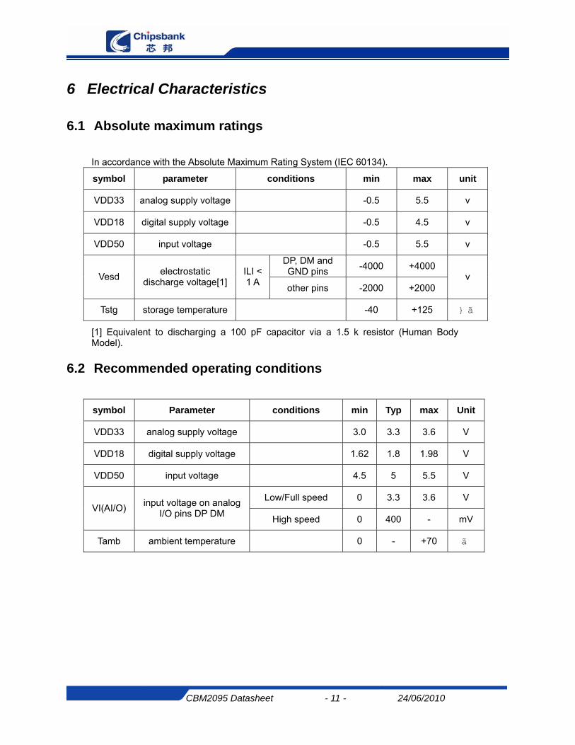
6.1 Absolute maximum ratings
In accordance with the Absolute Maximum Rating System (IEC 60134).
symbol parameter conditions min max unit
VDD33 analog supply voltage -0.5 5.5 v
VDD18 digital supply voltage -0.5 4.5 v
VDD50 input voltage -0.5 5.5 v
DP, DM and GND pins -4000 +4000
Vesd electrostatic discharge voltage[1]
ILI < 1 A other pins -2000 +2000
v
Tstg storage temperature -40 +125 ℃
[1] Equivalent to discharging a 100 pF capacitor via a 1.5 k resistor (Human Body Model).
6.2 Recommended operating conditions
symbol Parameter conditions min Typ max Unit
VDD33 analog supply voltage 3.0 3.3 3.6 V
VDD18 digital supply voltage 1.62 1.8 1.98 V
VDD50 input voltage 4.5 5 5.5 V
Low/Full speed 0 3.3 3.6 V VI(AI/O) input voltage on analog
I/O pins DP DM High speed 0 400 - mV
Tamb ambient temperature 0 - +70 ℃
CBM2095 Datasheet - 11 - 24/06/2010

6.3 Static characteristics
All parameters are measured at VCCA = VCCD = 3.0 to 3.6 V; VAGND = VDGND = 0 V; Tamb = 40 to 85 ℃;
symbol Parameter Conditions min Typ max Unit
Full-speed transmitting and receiving; - 29.5 -
ICC operating supply current high-speed transmitting and
receiving - 50 mA
ICC(susp) suspend supply current in suspend mode - 500 uA
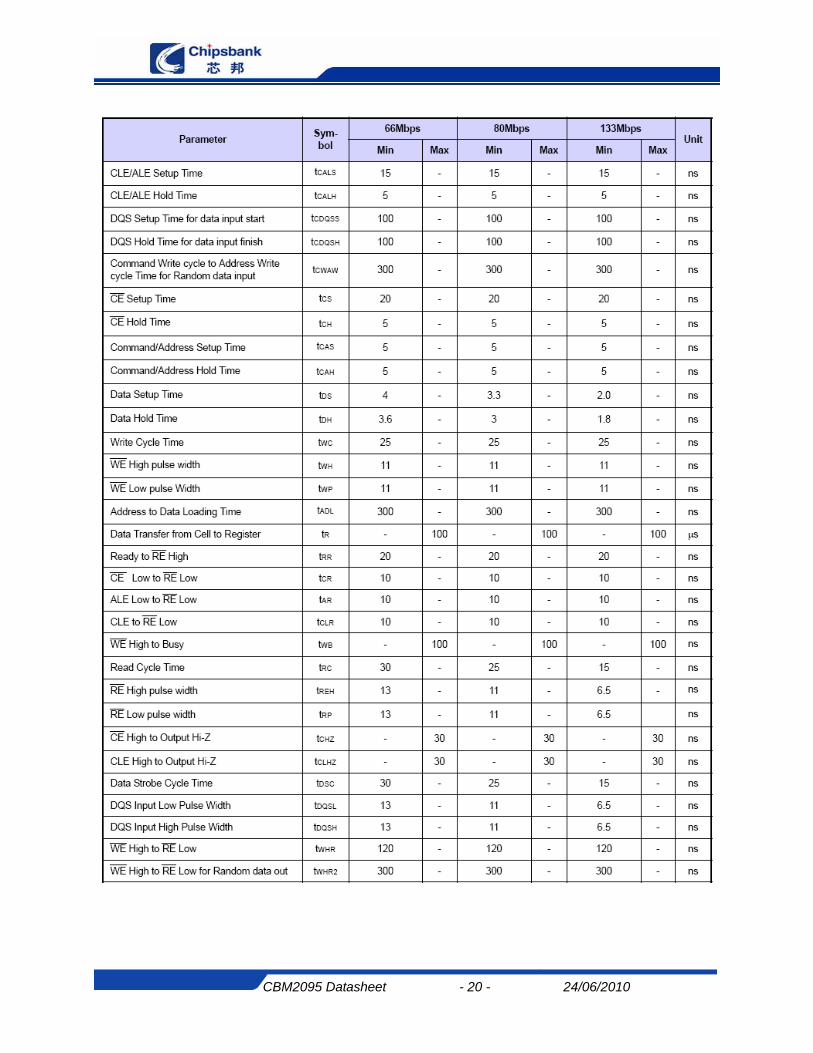
6.4 Dynamic characteristics
6.4.1 Normal NAND FLASH Dynamic characteristics
All parameters are measured at VCCA = VCCD = 3.0 to 3.6 V; VAGND = VDGND = 0 V; Tamb = -40 to 85 ℃ ;
symbol Parameter conditions min Typ max Unit
Ts(FDATA*) FDATA* setup time relative to rising FWRN* edge
Configured by firmware 8 33 75 ns
Th(FDATA*) FDATA* hold time relative to falling FWRN* edge
Configured by firmware 8 33 75 ns
Ts (FCLE*) FCLE* setup time relative to falling FWRN* edge
Configured by firmware 8 16 25 ns
Th (FCLE*) FCLE* hold time relative to rising FWRN* edge
Configured by firmware 10 16 75 ns
Ts (FALE*) FALE* setup time relative to falling FWRN* edge
Configured by firmware 8 16 25 ns
Th (FALE*) FALE* hold time relative to rising FWRN* edge
Configured by firmware 10 16 75 ns
Ts (FCEN*) FCEN* setup time relative to falling FWRN* edge
Configured by firmware - 99 ns
Tpw (FWRN*) FWRN* Pulse Width Configured by firmware 8 33 75 ns
Thh (FWRN*) FWRN* high hold time Configured by firmware 8 33 75 ns
Ta(FDATA*) FDATA* access time
relative to falling FRDN* edge
-5 0 5 ns
Tpw (FRDN*) FWRN* Pulse Width Configured by firmware 8 33 75 ns
Thh (FRDN*) FWRN* high hold time Configured by firmware 8 33 75 ns
CBM2095 Datasheet - 12 - 24/06/2010

Timing diagram for Writing of Data
Timing diagram for Reading of Data
CBM2095 Datasheet - 13 - 24/06/2010
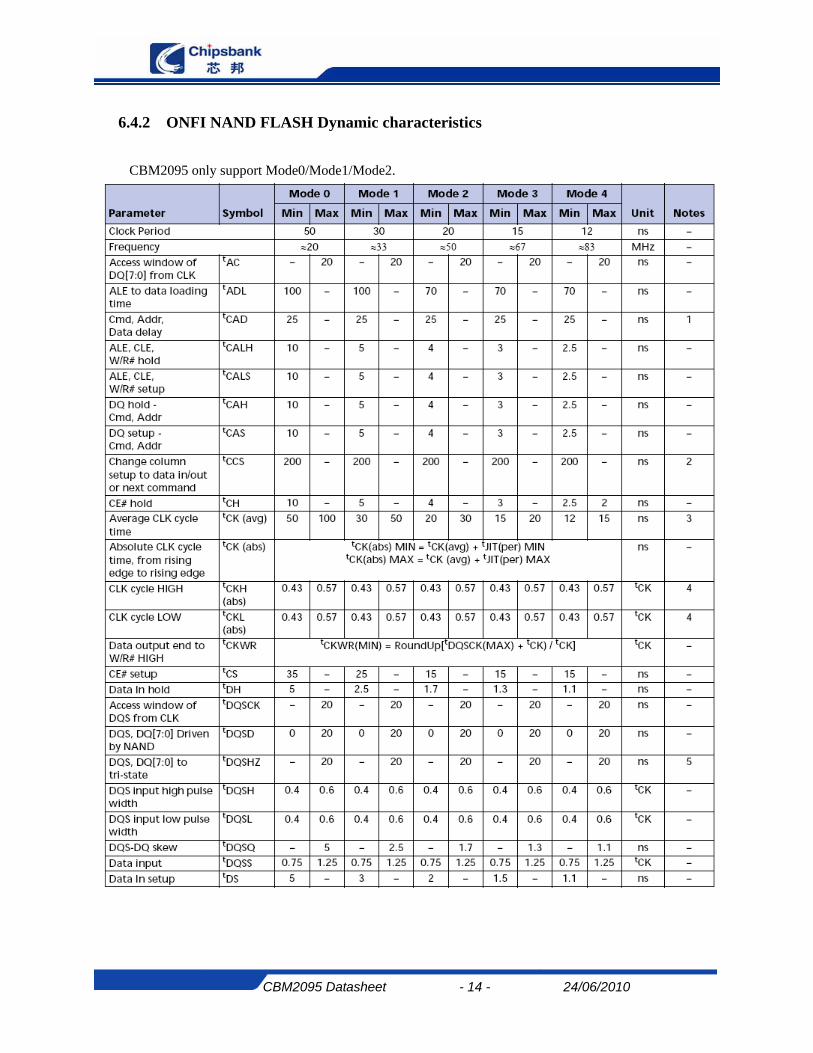
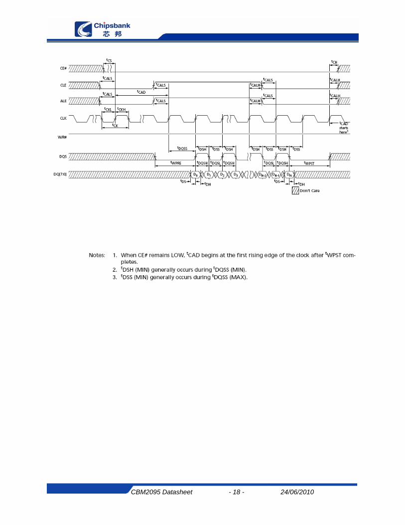
6.4.2 ONFI NAND FLASH Dynamic characteristics
CBM2095 only support Mode0/Mode1/Mode2.
CBM2095 Datasheet - 14 - 24/06/2010

CBM2095 Datasheet - 15 - 24/06/2010

CBM2095 Datasheet - 16 - 24/06/2010

CBM2095 Datasheet - 17 - 24/06/2010
CBM2095 Datasheet - 18 - 24/06/2010
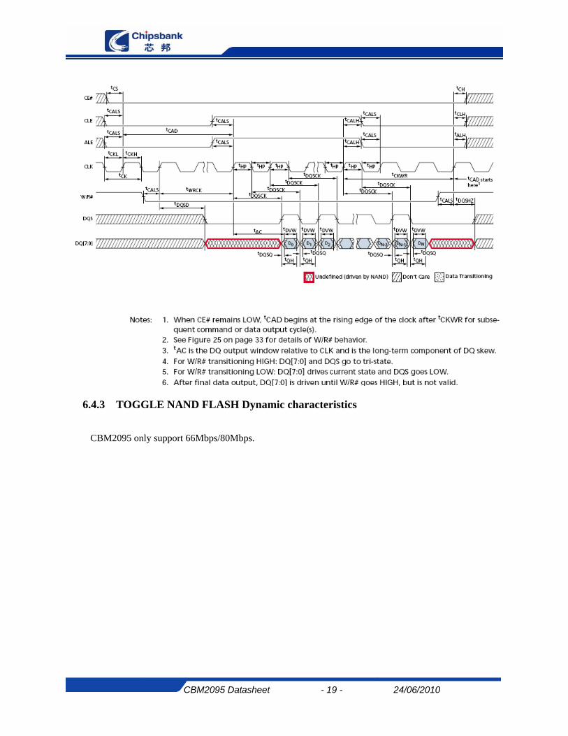
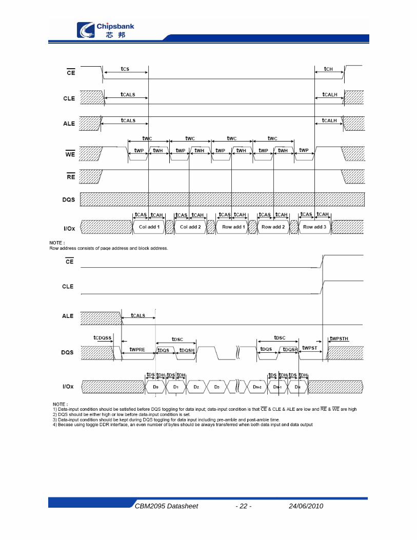
6.4.3 TOGGLE NAND FLASH Dynamic characteristics
CBM2095 only support 66Mbps/80Mbps.
CBM2095 Datasheet - 19 - 24/06/2010
CBM2095 Datasheet - 20 - 24/06/2010

CBM2095 Datasheet - 21 - 24/06/2010
CBM2095 Datasheet - 22 - 24/06/2010

CBM2095 Datasheet - 23 - 24/06/2010
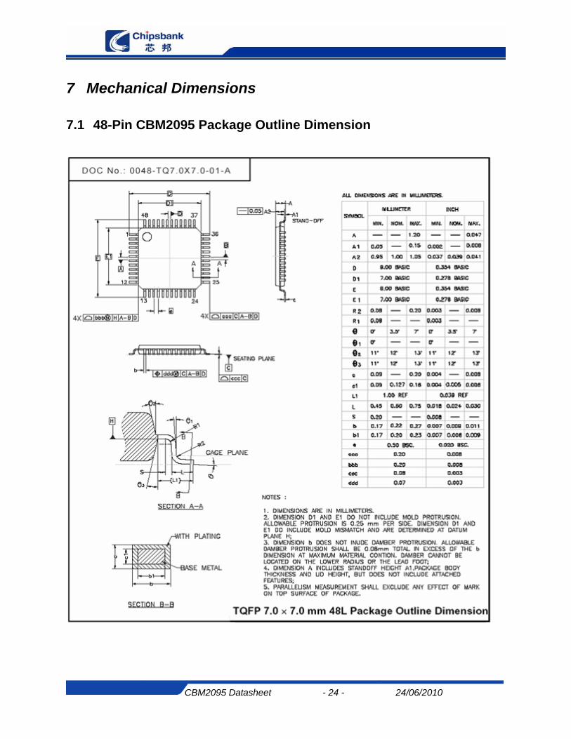
7 Mechanical Dimensions
7.1 48-Pin CBM2095 Package Outline Dimension
CBM2095 Datasheet - 24 - 24/06/2010

8 Copyright Notice
Copyright by Shenzhen Chipsbank Technologies Co.,Ltd. All Rights Reserved.
Right to make changes —Shenzhen Chipsbank Technologies Co.,Ltd. reserves the right to make changes in the products - including circuits, standard cells, and/or software - described or contained herein in order to improve design and/or performance. The information contained in this manual is provided for the general use by our customers. Our customers should be aware that the personal computer field is the subject of many patents. Our customers should ensure that they take appropriate action so that their use of our products does not infringe upon any patents. It is the policy of Shenzhen Chipsbank Technologies Co.,Ltd. to respect the valid patent rights of third parties and not to infringe upon or assist others to infringe upon such rights.
This manual is copyrighted by Shenzhen Chipsbank Technologies Co.,Ltd. You may not reproduce, transmit, transcribe, store in a retrieval system, or translate into any language, in any form or by any means, electronic, mechanical, magnetic, optical, chemical, manual, or otherwise, any part of this publication without the expressly written permission from Shenzhen Chipsbank Technologies Co.,Ltd.
CBM2095 Datasheet - 25 - 24/06/2010