ccd-in-cmos tdi & multispectral tdi imaging multispectral...ccd-in-cmos tdi & multispectral...
TRANSCRIPT

CCD-IN-CMOS TDI & MULTISPECTRAL TDI IMAGINGImec integrates the advantages of CCD and CMOS in a single sensor and this combined with wafer-level or glass-level spectral filters. The result is a next-generation multispectral TDI imager. To maximally support your product development, we offer various business models ranging from full-custom design to off-the-shelf prototype TDI sensors and evaluation cameras with a customized number of bands.
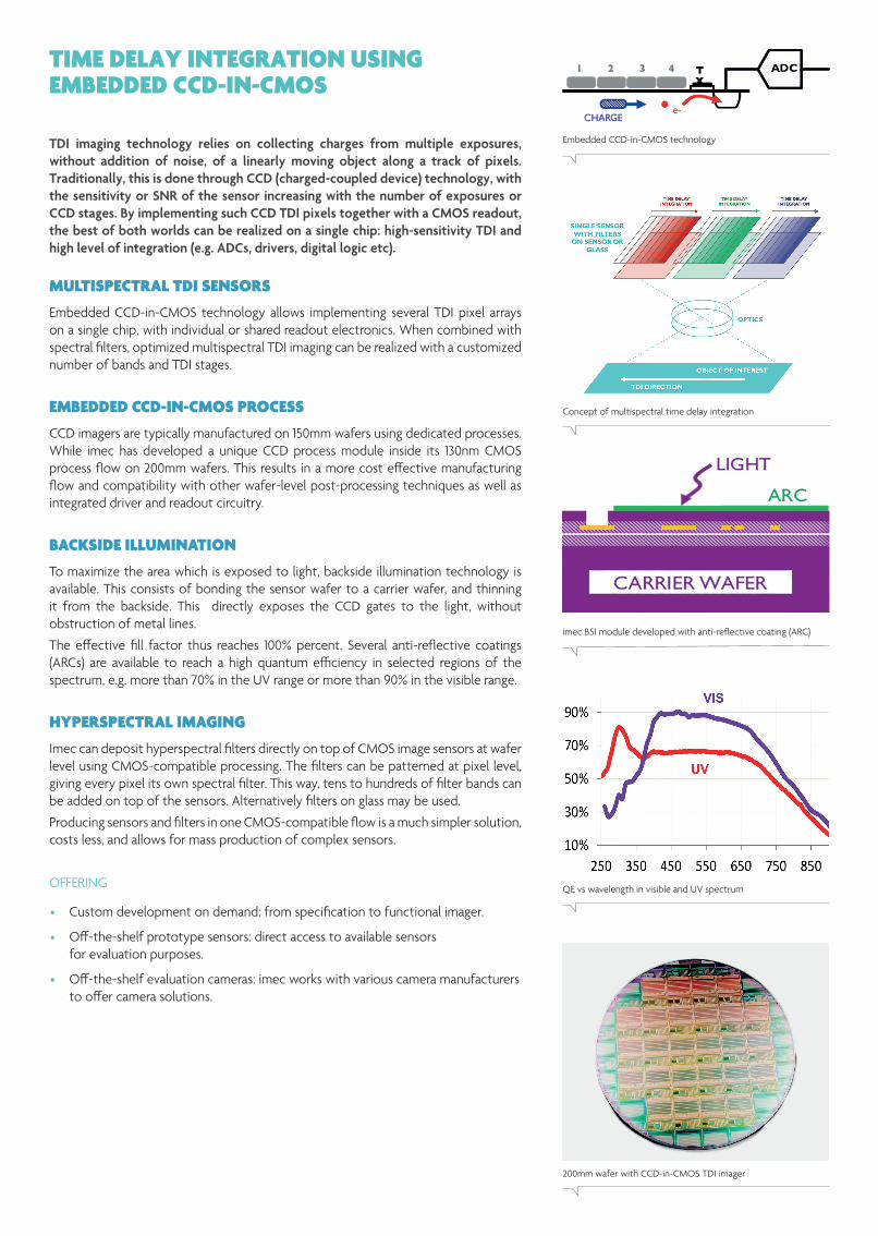
Embedded CCD-in-CMOS technology
Concept of multispectral time delay integration
TIME DELAY INTEGRATION USING EMBEDDED CCD-IN-CMOS
TDI imaging technology relies on collecting charges from multiple exposures, without addition of noise, of a linearly moving object along a track of pixels. Traditionally, this is done through CCD (charged-coupled device) technology, with the sensitivity or SNR of the sensor increasing with the number of exposures or CCD stages. By implementing such CCD TDI pixels together with a CMOS readout, the best of both worlds can be realized on a single chip: high-sensitivity TDI and high level of integration (e.g. ADCs, drivers, digital logic etc).
MULTISPECTRAL TDI SENSORSEmbedded CCD-in-CMOS technology allows implementing several TDI pixel arrays on a single chip, with individual or shared readout electronics. When combined with spectral filters, optimized multispectral TDI imaging can be realized with a customized number of bands and TDI stages.
EMBEDDED CCD-IN-CMOS PROCESSCCD imagers are typically manufactured on 150mm wafers using dedicated processes. While imec has developed a unique CCD process module inside its 130nm CMOS process flow on 200mm wafers. This results in a more cost effective manufacturing flow and compatibility with other wafer-level post-processing techniques as well as integrated driver and readout circuitry.
BACKSIDE ILLUMINATIONTo maximize the area which is exposed to light, backside illumination technology is available. This consists of bonding the sensor wafer to a carrier wafer, and thinning it from the backside. This directly exposes the CCD gates to the light, without obstruction of metal lines.The effective fill factor thus reaches 100% percent. Several anti-reflective coatings (ARCs) are available to reach a high quantum efficiency in selected regions of the spectrum, e.g. more than 70% in the UV range or more than 90% in the visible range.
HYPERSPECTRAL IMAGINGImec can deposit hyperspectral filters directly on top of CMOS image sensors at wafer level using CMOS-compatible processing. The filters can be patterned at pixel level, giving every pixel its own spectral filter. This way, tens to hundreds of filter bands can be added on top of the sensors. Alternatively filters on glass may be used. Producing sensors and filters in one CMOS-compatible flow is a much simpler solution, costs less, and allows for mass production of complex sensors.
OFFERING
• Custom development on demand: from specification to functional imager.
• Off-the-shelf prototype sensors: direct access to available sensors for evaluation purposes.
• Off-the-shelf evaluation cameras: imec works with various camera manufacturers to offer camera solutions.
imec BSI module developed with anti-reflective coating (ARC)
QE vs wavelength in visible and UV spectrum
200mm wafer with CCD-in-CMOS TDI imager
TDI sensor with integrated RGB fi lterPackaged 7 band TDI sensor
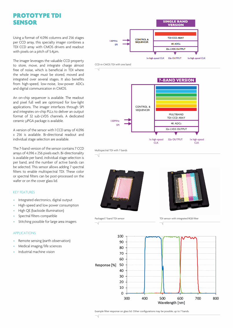
PROTOTYPE TDI SENSOR
Using a format of 4,096 columns and 256 stages per CCD array, this specialty imager combines a TDI CCD array with CMOS drivers and readout with pixels on a pitch of 5.4μm.
The imager leverages the valuable CCD property to store, move, and integrate charge almost free of noise, which is benefi cial in TDI where the whole image must be stored, moved and integrated over several stages. It also benefi ts from high-speed, low-noise, low-power ADCs and digital communication in CMOS.
An on-chip sequencer is available. The readout and pixel full well are optimized for low-light applications. The imager interfaces through SPI and integrates on-chip PLLs to deliver an output format of 32 sub-LVDS channels. A dedicated ceramic μPGA package is available.
A version of the sensor with 1 CCD array of 4,096 x 256 is available. Bi-directional readout and individual stage selection are available.
The 7-band version of the sensor contains 7 CCD arrays of 4,096 x 256 pixels each. Bi-directionality is available per band, individual stage selection is per band, and the number of active bands can be selected. This sensor allows adding 7 spectral fi lters to enable multispectral TDI. These color or spectral fi lters can be post-processed on the wafer or on the cover glass lid.
KEY FEATURES
• Integrated electronics, digital output• High-speed and low power consumption• High QE (backside illumination) • Spectral fi lters compatible
• Stitching possible for large area imagers
APPLICATIONS
• Remote sensing (earth observation)• Medical imaging/life sciences
• Industrial machine vision
CCD-in-CMOS TDI with one band
Multispectral TDI with 7 bands
Example fi lter response on glass lid. Other confi gurations may be possible, up to 7 bands.

imec • Kapeldreef 75 • 3001 Leuven • Belgium • www.imec.be
DISCLAIMER - This information is provided ‘AS IS’, without any representation or warranty. Imec is a registered trademark for the activities of IMEC International (a legal entity set up under Belgian law as a “stichting van openbaar nut”), imec Belgium (IMEC vzw supported by the Flemish Government), imec the Netherlands (Stichting IMEC Nederland, part of Holst Centre which is supported by the Dutch Government), imec Taiwan (IMEC Taiwan Co.) and imec China (IMEC Microelectronics (Shanghai) Co. Ltd.) and imec India (Imec India Private Limited), imec Florida (IMEC USA nanoelectronics design center).
PIET DE [email protected]
+32 16 28 17 05
SPECIFICATIONS
Size 77mm x 77mm x 99mm
Interface 4 x CXP-6
Mount type F-mount
OFF-THE-SHELF EVALUATION CAMERA A prototype camera is available for evaluation of the sensors. The camera is compatible with the available TDI sensors. A 4x lane CoaxPress is provided with firmware and simple API.
Off-the-shelf evaluation camera
OFF-THE-SHELF PROTOTYPE TDI SENSORSPECIFICATION TARGET
SENSOR SPEC TARGET 1-BAND 7-BAND
Array size 4k x 256 stages per band
Pixel size 5.4μm
Stage selection 1-to-256 reconfigurable per band individually
Line rate Up to 300kHz Up to 300kHz aggregate e.g. 42kHz for 7-bands active)
Operation mode Bi-directional Bi-directional Individual band activation
Power < 3W
Package type Ceramic μPGA
Output type 32 x sub-LVDS
Control SPI
Dynamic range / SNR > 60dB / 43dB
CTE > 99.995% @ 300 kHz
QE 60% (UV) - 90% (VIS)
Color filters Processed on wafer or glass lid per band (custom)Package drawing TDI sensor