cdcvf25081 3.3-v phased-lock loop clock driver · voh high-level output voltagehigh level out ut...
TRANSCRIPT

CDCVF250813.3-V PHASED-LOCK LOOP CLOCK DRIVER
SCAS671A – OCTOBER 2001 – REVISED FEBRUARY 2003
1POST OFFICE BOX 655303 • DALLAS, TEXAS 75265
Phase-Locked Loop-Based Zero-DelayBuffer
Operating Frequency: 8 MHz to 200 MHz
Low Jitter (Cycle-Cycle): ±100 ps Over theRange 66 MHz to 200 MHz
Distributes One Clock Input to Two Banksof Four Outputs
Auto Frequency Detection to DisableDevice (Power Down Mode)
Consumes Less Than 20 µA in Power DownMode
Operates From Single 3.3-V Supply
Industrial Temperature Range –40°C to85°C
25-Ω On-Chip Series Damping Resistors
No External RC Network Required
Spread Spectrum Clock Compatible (SSC)
Available in 16-Pin TSSOP or 16-Pin SOICPackages
description
The CDCVF25081 is a high-performance, low-skew, low-jitter, phase-lock loop clock driver. It uses a PLL toprecisely align, in both frequency and phase, the output clocks to the input clock signal. The CDCVF25081operates from a nominal supply voltage of 3.3 V. The device also includes integrated series-damping resistorsin the output drivers that make it ideal for driving point-to-point loads.
Two banks of four outputs each provide low-skew, low-jitter copies of CLKIN. All outputs operate at the samefrequency. Output duty cycles are adjusted to 50%, independent of duty cycle at CLKIN. The deviceautomatically goes into power-down mode when no input signal is applied to CLKIN and the outputs go into alow state. Unlike many products containing PLLs, the CDCVF25081 does not require an external RC network.The loop filter for the PLL is included on-chip, minimizing component count, space, and cost.
Because it is based on a PLL circuitry, the CDCVF25081 requires a stabilization time to achieve phase lock ofthe feedback signal to the reference signal. This stabilization is required following power up and application ofa fixed-frequency signal at CLKIN and any following changes to the PLL reference.
The CDCVF25081 is characterized for operation from -40°C to 85°C.
FUNCTION TABLE
S2 S1 1Y0–1Y3 2Y0–2Y3 OUTPUT SOURCE PLL SHUTDOWN
0 0 Hi-Z Hi-Z N/A. Yes
0 1 Active Hi-Z PLL† No
1 0 Active Active Input clock (PLL bypass) Yes
1 1 Active Active PLL† No† CLK input frequency < 2 MHz switches the outputs to low level
Copyright 2001 – 2003, Texas Instruments IncorporatedPRODUCTION DATA information is current as of publication date.Products conform to specifications per the terms of Texas Instrumentsstandard warranty. Production processing does not necessarily includetesting of all parameters.
Please be aware that an important notice concerning availability, standard warranty, and use in critical applications ofTexas Instruments semiconductor products and disclaimers thereto appears at the end of this data sheet.
1
2
3
4
5
6
78
16
15
14
13
12
11
109
CLKIN1Y01Y1VDDGND2Y02Y1S2
FBIN1Y31Y2VDDGND2Y32Y2S1
D PACKAGE (SOIC)PW PACKAGE (TSSOP)
(TOP VIEW)

CDCVF250813.3-V PHASED-LOCK LOOP CLOCK DRIVER
SCAS671A – OCTOBER 2001 – REVISED FEBRUARY 2003
2 POST OFFICE BOX 655303 • DALLAS, TEXAS 75265
Terminal Functions
TERMINALTYPE DESCRIPTION
NAME PIN NO.TYPE DESCRIPTION
1Y[0:3] 2, 3, 14, 15 O Bank 1Yn clock outputs. These outputs are low-skew copies of CLKIN. Each output has an integrated25-Ω series-damping resistor.
2Y[0:3] 6, 7, 10, 11 O Bank 2Yn clock outputs. These outputs are low-skew copies of CLKIN. Each output has an integrated25-Ω series-damping resistor.
CLKIN 1 I Clock input. CLKIN provides the clock signal to be distributed by the CDCVF25081 clock driver. CLKIN isused to provide the reference signal to the integrated PLL that generates the output signal. CLKIN musthave a fixed frequency and phase in order for the PLL to acquire lock. Once the circuit is powered up anda valid signal is applied, a stabilization time is required for the PLL to phase lock the feedback signal toCLKIN.
FBIN 16 I Feedback input. FBIN provides the feedback signal to the internal PLL. FBIN must be wired to one of theoutputs to complete the feedback loop of the internal PLL. The integrated PLL synchronizes the FBIN andoutput signal so there is nominally zero-delay from input clock to output clock.
GND 5, 12 Ground Ground
S1, S2 9, 8 I Select pins to determine mode of operation. See the FUNCTION TABLE for mode selection options.
VDD 4, 13 Power Supply voltage. The supply voltage range is 3 V to 3.6 V

CDCVF250813.3-V PHASED-LOCK LOOP CLOCK DRIVER
SCAS671A – OCTOBER 2001 – REVISED FEBRUARY 2003
3POST OFFICE BOX 655303 • DALLAS, TEXAS 75265
functional block diagram
2 1Y0
PLL16
FBIN
25 Ω
3 1Y125 Ω
141Y2
25 Ω
151Y3
25 Ω
MUX
1CLKIN
InputSelect
Decoding
8S2
9S1
6 2Y025 Ω
72Y1
25 Ω
102Y2
25 Ω
112Y3
25 Ω

CDCVF250813.3-V PHASED-LOCK LOOP CLOCK DRIVER
SCAS671A – OCTOBER 2001 – REVISED FEBRUARY 2003
4 POST OFFICE BOX 655303 • DALLAS, TEXAS 75265
absolute maximum ratings over operating free-air temperature (unless otherwise noted)†
Supply voltage range, VDD –0.5 V to 4.6 V. . . . . . . . . . . . . . . . . . . . . . . . . . . . . . . . . . . . . . . . . . . . . . . . . . . . . . . . . Input voltage range, VI (see Notes 1 and 2) –0.5 V to 4.6 V. . . . . . . . . . . . . . . . . . . . . . . . . . . . . . . . . . . . . . . . . . Output voltage range, VO (see Notes 1 and 2) –0.5 V to VDD + 0.5 V. . . . . . . . . . . . . . . . . . . . . . . . . . . . . . . . . . Input clamp current, IIK (VI < 0) –50 mA. . . . . . . . . . . . . . . . . . . . . . . . . . . . . . . . . . . . . . . . . . . . . . . . . . . . . . . . . . . Output clamp current, IOK (VO < 0) –50 mA. . . . . . . . . . . . . . . . . . . . . . . . . . . . . . . . . . . . . . . . . . . . . . . . . . . . . . . . Continuous total output current, IO (VO = 0 to VDD) –50 mA. . . . . . . . . . . . . . . . . . . . . . . . . . . . . . . . . . . . . . . . . . Package thermal impedance, θJA (see Note 3): PW package 147°C/W. . . . . . . . . . . . . . . . . . . . . . . . . . . . . . .
D package 112°C/W. . . . . . . . . . . . . . . . . . . . . . . . . . . . . . . . . Storage temperature range, Tstg –65°C to 150°C. . . . . . . . . . . . . . . . . . . . . . . . . . . . . . . . . . . . . . . . . . . . . . . . . . .
† Stresses beyond those listed under “absolute maximum ratings” may cause permanent damage to the device. These are stress ratings only, andfunctional operation of the device at these or any other conditions beyond those indicated under “recommended operating conditions” is notimplied. Exposure to absolute-maximum-rated conditions for extended periods may affect device reliability.
NOTES: 1. The input and output negative voltage ratings may be exceeded if the input and output clamp-current ratings are observed.2. This value is limited to 4.6 V maximum.3. The package thermal impedance is calculated in accordance with JESD 51.
recommended operating conditions
MIN NOM MAX UNIT
Supply voltage, VDD 3 3.3 3.6 V
Low level input voltage, VIL 0.8 V
High level input voltage, VIH 2 V
Input voltage, VI 0 3.6 V
High-level output current, IOH –12 mA
Low-level output current, IOL 12 mA
Operating free-air temperature, TA -40 85 °C
timing requirements over recommended ranges of supply voltage, load and operating free-airtemperature
MIN NOM MAX UNIT
Clock frequency fCL = 25 pF 8 100
MHzClock frequency, fclk CL = 15 pF 66 200MHz

CDCVF250813.3-V PHASED-LOCK LOOP CLOCK DRIVER
SCAS671A – OCTOBER 2001 – REVISED FEBRUARY 2003
5POST OFFICE BOX 655303 • DALLAS, TEXAS 75265
electrical characteristics over recommended operating free-air temperature range (unlessotherwise noted)
PARAMETER TEST CONDITIONS MIN TYP† MAX UNIT
VIK Input voltage VDD = 3 V, II = -18 mA –1.2 V
II Input current VI = 0 V or VDD ±5 µA
IPD‡ Power down current fCLKIN = 0 MHz, VDD = 3.3 V 20 µA
IOZ Output 3-state Vo = 0 V or VDD, VDD = 3.6 V ±5 µA
CI Input capacitance at FBIN, CLKIN VI = 0 V or VDD 4 pF
CI Input capacitance at S1, S2 VI = 0 V or VDD 2.2 pF
CO Output capacitance VI = 0 V or VDD 3 pF
VDD = min to max, IOH = -100 µA VDD – 0.2
VOH High-level output voltage VDD = 3 V, IOH = -12 mA 2.1 VVOH High level out ut voltage
VDD = 3 V, IOH = -6 mA 2.4
V
VDD = min to max, IOL = 100 µA 0.2
VOL Low-level output voltage VDD = 3 V, IOL = 12 mA 0.8 VVOL Low level out ut voltage
VDD = 3 V, IOL = 6 mA 0.55
V
VDD = 3 V, VO = 1 V –24
IOH High-level output current VDD = 3.3 V, VO = 1.65 V –30 mAIOH High level out ut current
VDD = 3.6 V, VO = 3.135 V -15
mA
VDD = 3 V, VO = 1.95 V 26
IOL Low-level output current VDD = 3.3 V, VO = 1.65 V 33 mAOL
VDD = 3.6 V, VO = 0.4 V 14† All typical values are at respective nominal VDD.‡ For IDD over frequency see Figure 7.

CDCVF250813.3-V PHASED-LOCK LOOP CLOCK DRIVER
SCAS671A – OCTOBER 2001 – REVISED FEBRUARY 2003
6 POST OFFICE BOX 655303 • DALLAS, TEXAS 75265
switching characteristics over recommended operating free-air temperature range (unlessotherwise noted)
PARAMETER TEST CONDITIONS MIN TYP† MAX UNIT
t(lock) PLL lock time f = 100 MHz 10 µs
t Phase offset (CLKIN to FBIN)
f = 8 MHz to 66 MHz,Vth = VDD/2 (see Note 5)
–200 200
pst(phoffset) Phase offset (CLKIN to FBIN)f = 66 MHz to 200 MHz, Vth = VDD/2 (see Note 5)
–150 150ps
tPLH Low-to-high level output propagation delay S2 = High, S1 = Low (PLL bypass) 2.5 6 ns
tPHL High-to-low level output propagation delayS2 = High, S1 = Low (PLL by ass) f = 1 MHz, CL = 25 pF
tsk(o) Output skew (Yn to Yn) (see Note 4) 150 ps
t Part to part skewS2 = high, S1 = high (PLL mode) 600
pstsk(pp) Part-to-part skewS2 = high, S1 = low (PLL bypass) 700
ps
f = 66 MHz to 200 MHz, CL = 15 pF ±100
tjit(cc) Jitter (cycle-to-cycle) f = 66 MHz to 100 MHz, CL = 25 pFf = 8 MHz to 66 MHz (see Figure 6)
±150ps
odc Output duty cycle f = 8 MHz to 200 MHz 43% 57%
tsk(p) Pulse skewS2 = High, S1 = low (PLL bypass)f = 1 MHz, CL = 25 pF
0.7 ns
t Rise time rateCL = 15 pF, See Figure 4 0.8 3.3
V/nstr Rise time rateCL = 25 pF, See Figure 4 0.5 2
V/ns
t Fall time rateCL = 15 pF, See Figure 4 0.8 3.3
V/nstf Fall time rateCL = 25 pF, See Figure 4 0.5 2
V/ns
† All typical values are at respective nominal VDD.NOTES: 4. The tsk(o) specification is only valid for equal loading of all outputs.
5. Similar waveform at CLKIN and FBIN are required. For phase displacement between CLKIN and Y-outputs see Figure 5.

CDCVF250813.3-V PHASED-LOCK LOOP CLOCK DRIVER
SCAS671A – OCTOBER 2001 – REVISED FEBRUARY 2003
7POST OFFICE BOX 655303 • DALLAS, TEXAS 75265
PARAMETER MEASUREMENT INFORMATION
NOTES: A. CL includes probe and jig capacitance.B. All input pulses are supplied by generators having the following characteristics: ZO = 50 Ω, tr < 1.2 ns, tf < 1.2 ns.C. The outputs are measured one at a time with one transition per measurement.
1000 Ω
From Output Under Test
VDD
1000 Ω
CL = 25 pF at f = 8 MHz to 100 MHzCL = 15 pF at f = 66 MHz to 200 MHz
Figure 1. Test Load Circuit
FBIN
50% VDD
VOL
VOH
CLKIN 0 V
VDD
50% VDD
t(phoffset)
Figure 2. Voltage Thresholds for Measurements, Phase Offset (PLL Mode)
NOTE: odc = t1/(t1 + t2) x 100%
50% VDD
Any Y
Any Y
tsk(0)
50% VDD
tsk(0)
50% VDD
t1
t2
Figure 3. Output Skew and Output Duty Cycle (PLL Mode)

CDCVF250813.3-V PHASED-LOCK LOOP CLOCK DRIVER
SCAS671A – OCTOBER 2001 – REVISED FEBRUARY 2003
8 POST OFFICE BOX 655303 • DALLAS, TEXAS 75265
PARAMETER MEASUREMENT INFORMATION
NOTE: tsk(p)=|tPLH–tPHL|
80%
Any Y
50% VDD20%
tf
VOL
VOH
tr
CLKIN 0 V
VDD
tPHL
50% VDD
tPLH
80%
50% VDD20%
Figure 4. Propagation Delay and Pulse Skew (Non-PLL Mode)
Figure 5
Cload Difference Between FBIN and Yn Pins – pF(CFB + 4 pF) – CYn
–150
–100
–50
0
50
100
–10 –8 –6 –4 –2 0 2 4 6 8 10
VDD = 3 V
Ph
ase
Dis
pla
cem
ent –
ps
PHASE DISPLACEMENTvs
CLOAD
VDD = 3.6 V
VDD = 3.3 V
Figure 6
f – Frequency – MHz
0
50
100
150
200
250
300
350
400
450
500
10 20 30 40 50 60 70 80 90 100
VDD = 3.3 VAll Outputs SwitchingCL(Yn) = 25 pF || 500 Ω
Cyc
le-t
o-C
ycle
Jit
ter
– p
s
CYCLE-TO-CYCLE JITTERvs
FREQUENCY

CDCVF250813.3-V PHASED-LOCK LOOP CLOCK DRIVER
SCAS671A – OCTOBER 2001 – REVISED FEBRUARY 2003
9POST OFFICE BOX 655303 • DALLAS, TEXAS 75265
PARAMETER MEASUREMENT INFORMATION
f – Frequency – MHz
0
20
40
60
80
100
120
140
160
180
0 20 40 60 80 100 120 140 160 180 200
VDD = 3 V to 3.6 VCL(Yn) = 15 pF || 500 ΩTA = –40°C to 85°C
I DD
– S
up
ply
cu
rren
t –
mA
SUPPLY CURRENTvs
FREQUENCY
VDD = 3.6 VTA = –40°C
VDD = 3.6 VTA = 85°C
VDD = 3 VTA = –40°C
VDD = 3 VTA = 85°C
Figure 7

PACKAGE OPTION ADDENDUM
www.ti.com 11-Apr-2013
Addendum-Page 1
PACKAGING INFORMATION
Orderable Device Status(1)
Package Type PackageDrawing
Pins PackageQty
Eco Plan(2)
Lead/Ball Finish MSL Peak Temp(3)
Op Temp (°C) Top-Side Markings(4)
Samples
CDCVF25081D ACTIVE SOIC D 16 40 Green (RoHS& no Sb/Br)
CU NIPDAU Level-1-260C-UNLIM -40 to 85 CKV25081
CDCVF25081DG4 ACTIVE SOIC D 16 40 Green (RoHS& no Sb/Br)
CU NIPDAU Level-1-260C-UNLIM -40 to 85 CKV25081
CDCVF25081DR ACTIVE SOIC D 16 2500 Green (RoHS& no Sb/Br)
CU NIPDAU Level-1-260C-UNLIM -40 to 85 CKV25081
CDCVF25081DRG4 ACTIVE SOIC D 16 2500 Green (RoHS& no Sb/Br)
CU NIPDAU Level-1-260C-UNLIM -40 to 85 CKV25081
CDCVF25081PW ACTIVE TSSOP PW 16 90 Green (RoHS& no Sb/Br)
CU NIPDAU Level-1-260C-UNLIM -40 to 85 CK081
CDCVF25081PWG4 ACTIVE TSSOP PW 16 90 Green (RoHS& no Sb/Br)
CU NIPDAU Level-1-260C-UNLIM -40 to 85 CK081
CDCVF25081PWR ACTIVE TSSOP PW 16 2000 Green (RoHS& no Sb/Br)
CU NIPDAU Level-1-260C-UNLIM -40 to 85 CK081
CDCVF25081PWRG4 ACTIVE TSSOP PW 16 2000 Green (RoHS& no Sb/Br)
CU NIPDAU Level-1-260C-UNLIM -40 to 85 CK081
(1) The marketing status values are defined as follows:ACTIVE: Product device recommended for new designs.LIFEBUY: TI has announced that the device will be discontinued, and a lifetime-buy period is in effect.NRND: Not recommended for new designs. Device is in production to support existing customers, but TI does not recommend using this part in a new design.PREVIEW: Device has been announced but is not in production. Samples may or may not be available.OBSOLETE: TI has discontinued the production of the device.
(2) Eco Plan - The planned eco-friendly classification: Pb-Free (RoHS), Pb-Free (RoHS Exempt), or Green (RoHS & no Sb/Br) - please check http://www.ti.com/productcontent for the latest availabilityinformation and additional product content details.TBD: The Pb-Free/Green conversion plan has not been defined.Pb-Free (RoHS): TI's terms "Lead-Free" or "Pb-Free" mean semiconductor products that are compatible with the current RoHS requirements for all 6 substances, including the requirement thatlead not exceed 0.1% by weight in homogeneous materials. Where designed to be soldered at high temperatures, TI Pb-Free products are suitable for use in specified lead-free processes.Pb-Free (RoHS Exempt): This component has a RoHS exemption for either 1) lead-based flip-chip solder bumps used between the die and package, or 2) lead-based die adhesive used betweenthe die and leadframe. The component is otherwise considered Pb-Free (RoHS compatible) as defined above.Green (RoHS & no Sb/Br): TI defines "Green" to mean Pb-Free (RoHS compatible), and free of Bromine (Br) and Antimony (Sb) based flame retardants (Br or Sb do not exceed 0.1% by weightin homogeneous material)
(3) MSL, Peak Temp. -- The Moisture Sensitivity Level rating according to the JEDEC industry standard classifications, and peak solder temperature.

PACKAGE OPTION ADDENDUM
www.ti.com 11-Apr-2013
Addendum-Page 2
(4) Multiple Top-Side Markings will be inside parentheses. Only one Top-Side Marking contained in parentheses and separated by a "~" will appear on a device. If a line is indented then it is acontinuation of the previous line and the two combined represent the entire Top-Side Marking for that device.
Important Information and Disclaimer:The information provided on this page represents TI's knowledge and belief as of the date that it is provided. TI bases its knowledge and belief on informationprovided by third parties, and makes no representation or warranty as to the accuracy of such information. Efforts are underway to better integrate information from third parties. TI has taken andcontinues to take reasonable steps to provide representative and accurate information but may not have conducted destructive testing or chemical analysis on incoming materials and chemicals.TI and TI suppliers consider certain information to be proprietary, and thus CAS numbers and other limited information may not be available for release.
In no event shall TI's liability arising out of such information exceed the total purchase price of the TI part(s) at issue in this document sold by TI to Customer on an annual basis.

TAPE AND REEL INFORMATION
*All dimensions are nominal
Device PackageType
PackageDrawing
Pins SPQ ReelDiameter
(mm)
ReelWidth
W1 (mm)
A0(mm)
B0(mm)
K0(mm)
P1(mm)
W(mm)
Pin1Quadrant
CDCVF25081DR SOIC D 16 2500 330.0 16.4 6.5 10.3 2.1 8.0 16.0 Q1
CDCVF25081PWR TSSOP PW 16 2000 330.0 12.4 6.9 5.6 1.6 8.0 12.0 Q1
PACKAGE MATERIALS INFORMATION
www.ti.com 14-Jul-2012
Pack Materials-Page 1
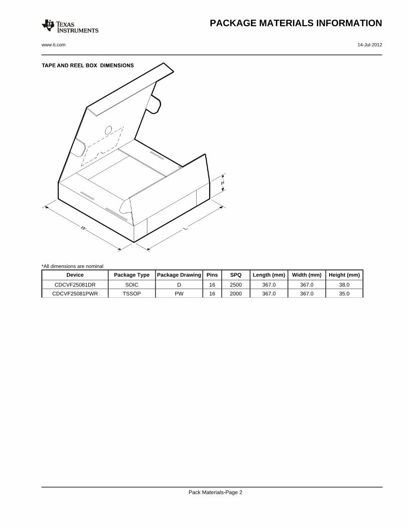
*All dimensions are nominal
Device Package Type Package Drawing Pins SPQ Length (mm) Width (mm) Height (mm)
CDCVF25081DR SOIC D 16 2500 367.0 367.0 38.0
CDCVF25081PWR TSSOP PW 16 2000 367.0 367.0 35.0
PACKAGE MATERIALS INFORMATION
www.ti.com 14-Jul-2012
Pack Materials-Page 2


IMPORTANT NOTICE
Texas Instruments Incorporated (TI) reserves the right to make corrections, enhancements, improvements and other changes to itssemiconductor products and services per JESD46, latest issue, and to discontinue any product or service per JESD48, latest issue. Buyersshould obtain the latest relevant information before placing orders and should verify that such information is current and complete.TI’s published terms of sale for semiconductor products (http://www.ti.com/sc/docs/stdterms.htm) apply to the sale of packaged integratedcircuit products that TI has qualified and released to market. Additional terms may apply to the use or sale of other types of TI products andservices.Reproduction of significant portions of TI information in TI data sheets is permissible only if reproduction is without alteration and isaccompanied by all associated warranties, conditions, limitations, and notices. TI is not responsible or liable for such reproduceddocumentation. Information of third parties may be subject to additional restrictions. Resale of TI products or services with statementsdifferent from or beyond the parameters stated by TI for that product or service voids all express and any implied warranties for theassociated TI product or service and is an unfair and deceptive business practice. TI is not responsible or liable for any such statements.Buyers and others who are developing systems that incorporate TI products (collectively, “Designers”) understand and agree that Designersremain responsible for using their independent analysis, evaluation and judgment in designing their applications and that Designers havefull and exclusive responsibility to assure the safety of Designers' applications and compliance of their applications (and of all TI productsused in or for Designers’ applications) with all applicable regulations, laws and other applicable requirements. Designer represents that, withrespect to their applications, Designer has all the necessary expertise to create and implement safeguards that (1) anticipate dangerousconsequences of failures, (2) monitor failures and their consequences, and (3) lessen the likelihood of failures that might cause harm andtake appropriate actions. Designer agrees that prior to using or distributing any applications that include TI products, Designer willthoroughly test such applications and the functionality of such TI products as used in such applications.TI’s provision of technical, application or other design advice, quality characterization, reliability data or other services or information,including, but not limited to, reference designs and materials relating to evaluation modules, (collectively, “TI Resources”) are intended toassist designers who are developing applications that incorporate TI products; by downloading, accessing or using TI Resources in anyway, Designer (individually or, if Designer is acting on behalf of a company, Designer’s company) agrees to use any particular TI Resourcesolely for this purpose and subject to the terms of this Notice.TI’s provision of TI Resources does not expand or otherwise alter TI’s applicable published warranties or warranty disclaimers for TIproducts, and no additional obligations or liabilities arise from TI providing such TI Resources. TI reserves the right to make corrections,enhancements, improvements and other changes to its TI Resources. TI has not conducted any testing other than that specificallydescribed in the published documentation for a particular TI Resource.Designer is authorized to use, copy and modify any individual TI Resource only in connection with the development of applications thatinclude the TI product(s) identified in such TI Resource. NO OTHER LICENSE, EXPRESS OR IMPLIED, BY ESTOPPEL OR OTHERWISETO ANY OTHER TI INTELLECTUAL PROPERTY RIGHT, AND NO LICENSE TO ANY TECHNOLOGY OR INTELLECTUAL PROPERTYRIGHT OF TI OR ANY THIRD PARTY IS GRANTED HEREIN, including but not limited to any patent right, copyright, mask work right, orother intellectual property right relating to any combination, machine, or process in which TI products or services are used. Informationregarding or referencing third-party products or services does not constitute a license to use such products or services, or a warranty orendorsement thereof. Use of TI Resources may require a license from a third party under the patents or other intellectual property of thethird party, or a license from TI under the patents or other intellectual property of TI.TI RESOURCES ARE PROVIDED “AS IS” AND WITH ALL FAULTS. TI DISCLAIMS ALL OTHER WARRANTIES ORREPRESENTATIONS, EXPRESS OR IMPLIED, REGARDING RESOURCES OR USE THEREOF, INCLUDING BUT NOT LIMITED TOACCURACY OR COMPLETENESS, TITLE, ANY EPIDEMIC FAILURE WARRANTY AND ANY IMPLIED WARRANTIES OFMERCHANTABILITY, FITNESS FOR A PARTICULAR PURPOSE, AND NON-INFRINGEMENT OF ANY THIRD PARTY INTELLECTUALPROPERTY RIGHTS. TI SHALL NOT BE LIABLE FOR AND SHALL NOT DEFEND OR INDEMNIFY DESIGNER AGAINST ANY CLAIM,INCLUDING BUT NOT LIMITED TO ANY INFRINGEMENT CLAIM THAT RELATES TO OR IS BASED ON ANY COMBINATION OFPRODUCTS EVEN IF DESCRIBED IN TI RESOURCES OR OTHERWISE. IN NO EVENT SHALL TI BE LIABLE FOR ANY ACTUAL,DIRECT, SPECIAL, COLLATERAL, INDIRECT, PUNITIVE, INCIDENTAL, CONSEQUENTIAL OR EXEMPLARY DAMAGES INCONNECTION WITH OR ARISING OUT OF TI RESOURCES OR USE THEREOF, AND REGARDLESS OF WHETHER TI HAS BEENADVISED OF THE POSSIBILITY OF SUCH DAMAGES.Unless TI has explicitly designated an individual product as meeting the requirements of a particular industry standard (e.g., ISO/TS 16949and ISO 26262), TI is not responsible for any failure to meet such industry standard requirements.Where TI specifically promotes products as facilitating functional safety or as compliant with industry functional safety standards, suchproducts are intended to help enable customers to design and create their own applications that meet applicable functional safety standardsand requirements. Using products in an application does not by itself establish any safety features in the application. Designers mustensure compliance with safety-related requirements and standards applicable to their applications. Designer may not use any TI products inlife-critical medical equipment unless authorized officers of the parties have executed a special contract specifically governing such use.Life-critical medical equipment is medical equipment where failure of such equipment would cause serious bodily injury or death (e.g., lifesupport, pacemakers, defibrillators, heart pumps, neurostimulators, and implantables). Such equipment includes, without limitation, allmedical devices identified by the U.S. Food and Drug Administration as Class III devices and equivalent classifications outside the U.S.TI may expressly designate certain products as completing a particular qualification (e.g., Q100, Military Grade, or Enhanced Product).Designers agree that it has the necessary expertise to select the product with the appropriate qualification designation for their applicationsand that proper product selection is at Designers’ own risk. Designers are solely responsible for compliance with all legal and regulatoryrequirements in connection with such selection.Designer will fully indemnify TI and its representatives against any damages, costs, losses, and/or liabilities arising out of Designer’s non-compliance with the terms and provisions of this Notice.
Mailing Address: Texas Instruments, Post Office Box 655303, Dallas, Texas 75265Copyright © 2017, Texas Instruments Incorporated