cdma and gsm / umts mini card - siongboon.com 3g module p… · 1.7 apr 2008 † removed ... gprs /...
TRANSCRIPT
CDMA and GSM / UMTS Mini Card
Hardware Integration Guide
Proprietary and Confidential
2130114Rev 1.14
Includes:
MC5725 MC8775
MC5725V MC8775V
MC5727 MC8780
MC5727V MC8781
MC5728V MC8790
MC8790V
MC8791V
MC8792V
MC8795V
MC8700

Preface
Important Notice
Due to the nature of wireless communications, transmission and reception of data can never be guaranteed. Data may be delayed, corrupted (i.e., have errors) or be totally lost. Although significant delays or losses of data are rare when wireless devices such as the Sierra Wireless modem are used in a normal manner with a well-constructed network, the Sierra Wireless modem should not be used in situations where failure to transmit or receive data could result in damage of any kind to the user or any other party, including but not limited to personal injury, death, or loss of property. Sierra Wireless accepts no responsibility for damages of any kind resulting from delays or errors in data transmitted or received using the Sierra Wireless modem, or for failure of the Sierra Wireless modem to transmit or receive such data.
Safety and Hazards
Do not operate the Sierra Wireless modem in areas where blasting is in progress, where explosive atmospheres may be present, near medical equipment, near life support equipment, or any equipment which may be susceptible to any form of radio interference. In such areas, the Sierra Wireless modem MUST BE POWERED OFF. The Sierra Wireless modem can transmit signals that could interfere with this equipment.
Do not operate the Sierra Wireless modem in any aircraft, whether the aircraft is on the ground or in flight. In aircraft, the Sierra Wireless modem MUST BE POWERED OFF. When operating, the Sierra Wireless modem can transmit signals that could interfere with various onboard systems.
Note: Some airlines may permit the use of cellular phones while the aircraft is on the ground and the door is open. Sierra Wireless modems may be used at this time.
The driver or operator of any vehicle should not operate the Sierra Wireless modem while in control of a vehicle. Doing so will detract from the driver or operator's control and operation of that vehicle. In some states and provinces, operating such communications devices while in control of a vehicle is an offence.
Limitation of Liability
The information in this manual is subject to change without notice and does not represent a commitment on the part of Sierra Wireless. SIERRA WIRELESS AND ITS AFFILIATES SPECIFICALLY DISCLAIM LIABILITY FOR ANY AND ALL DIRECT, INDIRECT, SPECIAL, GENERAL, INCIDENTAL, CONSEQUENTIAL, PUNITIVE OR EXEMPLARY DAMAGES INCLUDING, BUT NOT LIMITED TO, LOSS OF PROFITS OR REVENUE OR ANTICIPATED PROFITS OR REVENUE ARISING OUT OF THE USE OR INABILITY TO USE ANY SIERRA WIRELESS PRODUCT, EVEN IF SIERRA WIRELESS AND/OR ITS AFFILIATES HAS BEEN ADVISED OF THE POSSIBILITY OF SUCH DAMAGES OR THEY ARE FORESEEABLE OR FOR CLAIMS BY ANY THIRD PARTY.
Notwithstanding the foregoing, in no event shall Sierra Wireless and/or its affiliates aggregate liability arising under or in connection with the Sierra Wireless product, regardless of the number of events, occurrences, or claims giving rise to liability, be in excess of the price paid by the purchaser for the Sierra Wireless product.
Rev 1.14 Feb.10 Proprietary and Confidential 3 In the event of a discrepancy in values between this guide and the Product Specification Document (PSD), the PSD takes precedence.
CDMA and GSM / UMTS Mini Card Hardware Integration Guide
Patents Portions of this product may be covered by some or all of the following US patents:5,515,013 5,629,960 5,845,216 5,847,553 5,878,234 5,890,057 5,929,815 6,169,8846,191,741 6,199,168 6,339,405 6,359,591 6,400,336 6,516,204 6,561,851 6,643,5016,653,979 6,697,030 6,785,830 6,845,249 6,847,830 6,876,697 6,879,585 6,886,0496,968,171 6,985,757 7,023,878 7,053,843 7,106,569 7,145,267 7,200,512 7,295,1717, 287,162 D442,170 D459,303 D599,256 D560,911
and other patents pending.
This product includes technology licensed from QUALCOMM® 3G
Manufactured or sold by Sierra Wireless or its licensees under one or more patents licensed from InterDigital Group.
Copyright ©2010 Sierra Wireless. All rights reserved.
Trademarks AirCard® and Watcher® are registered trademarks of Sierra Wireless. Sierra Wireless, AirPrime, AirLink, AirVantage and the Sierra Wireless logo are trademarks of Sierra Wireless.
Windows® and Windows Vista® are registered trademarks of Microsoft Corporation.
Macintosh and Mac OS are registered trademarks of Apple Inc., registered in the U.S. and other countries.
QUALCOMM® is a registered trademark of QUALCOMM Incorporated. Used under license.
Other trademarks are the property of their respective owners.
Contact Information
Consult our website for up-to-date product descriptions, documentation, application notes, firmware upgrades, troubleshooting tips, and press releases:
www.sierrawireless.com
Sales Desk: Phone: 1-604-232-1488
Hours: 8:00 AM to 5:00 PM Pacific Time
E-mail: [email protected]
Post: Sierra Wireless13811 Wireless WayRichmond, BCCanada V6V 3A4
Fax: 1-604-231-1109
Web: www.sierrawireless.com
4 Proprietary and Confidential 2130114 In the event of a discrepancy in values between this guide and the Product Specification Document (PSD), the PSD takes precedence.
Preface
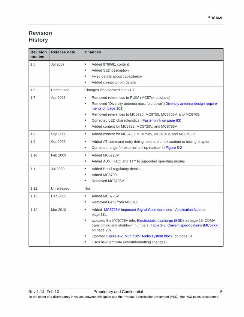
Revision History
Revision number
Release date Changes
1.5 Jul 2007 • Added 8780/81 content
• Added SED description
• Fixed details about capacitance
• Added connector pin details
1.6 Unreleased Changes incorporated into v1.7.
1.7 Apr 2008 • Removed references to RUIM (MC57xx products)
• Removed “Diversity antenna must fold down” (Diversity antenna design require-ments on page 101).
• Removed references to MC5720, MC8755, MC8755V, and MC8765.
• Corrected LED characteristics (Faster blink on page 63)
• Added content for MC5725, MC5725V, and MC8785V
1.8 Sep 2008 • Added content for MC8790, MC8790V, MC8791V, and MC8792V
1.9 Oct 2008 • Added AT command entry timing note and Linux content to testing chapter
• Corrected range for external pull up resistor in Figure 5-2
1.10 Feb 2009 • Added MC5728V
• Added AUX (HAC) and TTY to supported operating modes
1.11 Jul 2009 • Added Brazil regulatory details
• Added MC8700
• Removed MC8785V
1.12 Unreleased N/a
1.13 Dec 2009 • Added MC8795V
• Removed GPS from MC8700
1.14 Mar 2010 • Added MC5728V Important Signal Considerations - Application Note on page 111.
• Updated the MC5728V info: Electrostatic discharge (ESD) on page 18; CDMA transmitting and shutdown numbers (Table 2-3, Current specifications (MC57xx), on page 28).
• Updated Figure 4-2, MC5728V Audio system block, on page 54.
• Uses new template (layout/formatting changes)
Rev 1.14 Feb.10 Proprietary and Confidential 5 In the event of a discrepancy in values between this guide and the Product Specification Document (PSD), the PSD takes precedence.
CDMA and GSM / UMTS Mini Card Hardware Integration Guide
6 Proprietary and Confidential 2130114 In the event of a discrepancy in values between this guide and the Product Specification Document (PSD), the PSD takes precedence.
Rev 1.14 In the event
Contents
Introduction . . . . . . . . . . . . . . . . . . . . . . . . . . . . . . . . . . . . . . . . . . . . . . . . . . . .11
The Universal Development Kit . . . . . . . . . . . . . . . . . . . . . . . . . . . . . . . . . . 11
Required connectors . . . . . . . . . . . . . . . . . . . . . . . . . . . . . . . . . . . . . . . . . . 12
Guide organization . . . . . . . . . . . . . . . . . . . . . . . . . . . . . . . . . . . . . . . . . . . . 12
Related documents . . . . . . . . . . . . . . . . . . . . . . . . . . . . . . . . . . . . . . . . . . . 13
Power Interface . . . . . . . . . . . . . . . . . . . . . . . . . . . . . . . . . . . . . . . . . . . . . . . . .17
Overview of operation . . . . . . . . . . . . . . . . . . . . . . . . . . . . . . . . . . . . . . . . . 17
Power signals . . . . . . . . . . . . . . . . . . . . . . . . . . . . . . . . . . . . . . . . . . . . . .17
Electrostatic discharge (ESD) . . . . . . . . . . . . . . . . . . . . . . . . . . . . . . . . .18
Module power states . . . . . . . . . . . . . . . . . . . . . . . . . . . . . . . . . . . . . . . . . . 18
Disconnected state . . . . . . . . . . . . . . . . . . . . . . . . . . . . . . . . . . . . . . . . .19
Off state . . . . . . . . . . . . . . . . . . . . . . . . . . . . . . . . . . . . . . . . . . . . . . . . . .19
Normal state . . . . . . . . . . . . . . . . . . . . . . . . . . . . . . . . . . . . . . . . . . . . . . .19
Low power mode . . . . . . . . . . . . . . . . . . . . . . . . . . . . . . . . . . . . . . . . . . .19
Voltage monitoring state machine . . . . . . . . . . . . . . . . . . . . . . . . . . . . . .20
Temperature monitoring state machine . . . . . . . . . . . . . . . . . . . . . . . . . .22
Inrush currents . . . . . . . . . . . . . . . . . . . . . . . . . . . . . . . . . . . . . . . . . . . . . . . 24
Timing requirements. . . . . . . . . . . . . . . . . . . . . . . . . . . . . . . . . . . . . . . . . . . 26
Power ramp-up . . . . . . . . . . . . . . . . . . . . . . . . . . . . . . . . . . . . . . . . . . . .26
Power-up timing . . . . . . . . . . . . . . . . . . . . . . . . . . . . . . . . . . . . . . . . . . . .26
Transmit power wave form (GSM) . . . . . . . . . . . . . . . . . . . . . . . . . . . . . . . . 26
Current consumption . . . . . . . . . . . . . . . . . . . . . . . . . . . . . . . . . . . . . . . . . . 27
Current consumption overview . . . . . . . . . . . . . . . . . . . . . . . . . . . . . . . .27
Modes . . . . . . . . . . . . . . . . . . . . . . . . . . . . . . . . . . . . . . . . . . . . . . . . . . .35
SED (Smart Error Detection) . . . . . . . . . . . . . . . . . . . . . . . . . . . . . . . . . .35
Usage models . . . . . . . . . . . . . . . . . . . . . . . . . . . . . . . . . . . . . . . . . . . . .36
RF Integration . . . . . . . . . . . . . . . . . . . . . . . . . . . . . . . . . . . . . . . . . . . . . . . . . .37
RF connection . . . . . . . . . . . . . . . . . . . . . . . . . . . . . . . . . . . . . . . . . . . . . . . 39
Feb.10 Proprietary and Confidential 7of a discrepancy in values between this guide and the Product Specification Document (PSD), the PSD takes precedence.
CDMA and GSM / UMTS Mini Card Hardware Integration Guide
8 In the event
Ground connection . . . . . . . . . . . . . . . . . . . . . . . . . . . . . . . . . . . . . . . . . . . 40
Shielding . . . . . . . . . . . . . . . . . . . . . . . . . . . . . . . . . . . . . . . . . . . . . . . . . 40
Antenna and cabling . . . . . . . . . . . . . . . . . . . . . . . . . . . . . . . . . . . . . . . . 40
Interference and sensitivity . . . . . . . . . . . . . . . . . . . . . . . . . . . . . . . . . . . . . 41
Power supply noise . . . . . . . . . . . . . . . . . . . . . . . . . . . . . . . . . . . . . . . . . 41
Interference from other wireless devices . . . . . . . . . . . . . . . . . . . . . . . . . 41
Device-generated RF . . . . . . . . . . . . . . . . . . . . . . . . . . . . . . . . . . . . . . . 42
Methods to mitigate decreased Rx performance . . . . . . . . . . . . . . . . . . . 42
Radiated sensitivity measurement. . . . . . . . . . . . . . . . . . . . . . . . . . . . . . . . 43
Sierra Wireless’ sensitivity testing and desensitization investigation . . . 43
OTA test chamber configuration . . . . . . . . . . . . . . . . . . . . . . . . . . . . . . . 43
Path loss calculation . . . . . . . . . . . . . . . . . . . . . . . . . . . . . . . . . . . . . . . . 44
Positioning the DUT (Device Under Test) . . . . . . . . . . . . . . . . . . . . . . . . 44
Sensitivity vs. frequency . . . . . . . . . . . . . . . . . . . . . . . . . . . . . . . . . . . . . 45
Audio Interface . . . . . . . . . . . . . . . . . . . . . . . . . . . . . . . . . . . . . . . . . . . . . . . . . 51
System block diagrams . . . . . . . . . . . . . . . . . . . . . . . . . . . . . . . . . . . . . . 52
Modes of operation . . . . . . . . . . . . . . . . . . . . . . . . . . . . . . . . . . . . . . . . . 55
Sidetone support . . . . . . . . . . . . . . . . . . . . . . . . . . . . . . . . . . . . . . . . . . . 55
Gain distribution . . . . . . . . . . . . . . . . . . . . . . . . . . . . . . . . . . . . . . . . . . . 56
Echo cancellation support . . . . . . . . . . . . . . . . . . . . . . . . . . . . . . . . . . . . 56
Audio signal interface . . . . . . . . . . . . . . . . . . . . . . . . . . . . . . . . . . . . . . . 57
Audio function partitioning . . . . . . . . . . . . . . . . . . . . . . . . . . . . . . . . . . . . 58
Host / Module Interfaces . . . . . . . . . . . . . . . . . . . . . . . . . . . . . . . . . . . . . . . . . 59
Host interface pin details . . . . . . . . . . . . . . . . . . . . . . . . . . . . . . . . . . . . . . . 59
USB interface. . . . . . . . . . . . . . . . . . . . . . . . . . . . . . . . . . . . . . . . . . . . . . . . 61
USB handshaking . . . . . . . . . . . . . . . . . . . . . . . . . . . . . . . . . . . . . . . . . . 61
LED output . . . . . . . . . . . . . . . . . . . . . . . . . . . . . . . . . . . . . . . . . . . . . . . 62
USIM interface . . . . . . . . . . . . . . . . . . . . . . . . . . . . . . . . . . . . . . . . . . . . . 64
USIM operation . . . . . . . . . . . . . . . . . . . . . . . . . . . . . . . . . . . . . . . . . . . . 66
Extended AT commands . . . . . . . . . . . . . . . . . . . . . . . . . . . . . . . . . . . . . . . 67
Proprietary and Confidential 2130114of a discrepancy in values between this guide and the Product Specification Document (PSD), the PSD takes precedence.
Contents
Rev 1.14 In the event
Thermal Considerations . . . . . . . . . . . . . . . . . . . . . . . . . . . . . . . . . . . . . . . . . .71
Design Checklist . . . . . . . . . . . . . . . . . . . . . . . . . . . . . . . . . . . . . . . . . . . . . . . .73
Testing . . . . . . . . . . . . . . . . . . . . . . . . . . . . . . . . . . . . . . . . . . . . . . . . . . . . . . . .75
AT command entry timing requirement . . . . . . . . . . . . . . . . . . . . . . . . . .75
Acceptance testing. . . . . . . . . . . . . . . . . . . . . . . . . . . . . . . . . . . . . . . . . . . . 75
Test requirements . . . . . . . . . . . . . . . . . . . . . . . . . . . . . . . . . . . . . . . . . .75
Test procedure . . . . . . . . . . . . . . . . . . . . . . . . . . . . . . . . . . . . . . . . . . . . .76
Certification testing. . . . . . . . . . . . . . . . . . . . . . . . . . . . . . . . . . . . . . . . . . . . 76
Production testing. . . . . . . . . . . . . . . . . . . . . . . . . . . . . . . . . . . . . . . . . . . . . 77
Suggested manual functional test procedure . . . . . . . . . . . . . . . . . . . . . . . . 77
Suggested test plan procedure . . . . . . . . . . . . . . . . . . . . . . . . . . . . . . . .78
Testing RF transmission path—MC57xx . . . . . . . . . . . . . . . . . . . . . . . . .82
Testing RF transmission path—MC87xx . . . . . . . . . . . . . . . . . . . . . . . . .84
Testing RF Receive path—MC57xx . . . . . . . . . . . . . . . . . . . . . . . . . . . . .86
Testing RF Receive path—MC87xx . . . . . . . . . . . . . . . . . . . . . . . . . . . . .87
Testing GPS Receiver—MC8775V . . . . . . . . . . . . . . . . . . . . . . . . . . . . .90
Test Audio Loop-back—MC5725V / MC5727V / MC5728V / MC8775V / MC8790V / MC8791V / MC8792V / MC8795V . . . . . . . . . . . . . . . . . . . .91
Quality assurance testing . . . . . . . . . . . . . . . . . . . . . . . . . . . . . . . . . . . . . . . 93
Suggested testing equipment. . . . . . . . . . . . . . . . . . . . . . . . . . . . . . . . . . . . 93
Antenna Specification . . . . . . . . . . . . . . . . . . . . . . . . . . . . . . . . . . . . . . . . . . .97
Required antennas. . . . . . . . . . . . . . . . . . . . . . . . . . . . . . . . . . . . . . . . . . . . 97
Frequency bands . . . . . . . . . . . . . . . . . . . . . . . . . . . . . . . . . . . . . . . . . . .98
Antenna design . . . . . . . . . . . . . . . . . . . . . . . . . . . . . . . . . . . . . . . . . . . . . 100
General antenna design requirements . . . . . . . . . . . . . . . . . . . . . . . . . .101
Main antenna design requirements . . . . . . . . . . . . . . . . . . . . . . . . . . . .101
Diversity antenna design requirements . . . . . . . . . . . . . . . . . . . . . . . . .101
GPS antenna design requirements . . . . . . . . . . . . . . . . . . . . . . . . . . . .102
Feb.10 Proprietary and Confidential 9of a discrepancy in values between this guide and the Product Specification Document (PSD), the PSD takes precedence.
CDMA and GSM / UMTS Mini Card Hardware Integration Guide
10 In the event
Testing. . . . . . . . . . . . . . . . . . . . . . . . . . . . . . . . . . . . . . . . . . . . . . . . . . . . 102
Voltage Standing Wave Ratio (VSWR) . . . . . . . . . . . . . . . . . . . . . . . . . 103
Efficiency . . . . . . . . . . . . . . . . . . . . . . . . . . . . . . . . . . . . . . . . . . . . . . . . 104
Antenna-to-antenna isolation . . . . . . . . . . . . . . . . . . . . . . . . . . . . . . . . 104
Peak gain and radiation patterns . . . . . . . . . . . . . . . . . . . . . . . . . . . . . . 105
Fading correlation coefficient . . . . . . . . . . . . . . . . . . . . . . . . . . . . . . . . 105
Regulatory Information . . . . . . . . . . . . . . . . . . . . . . . . . . . . . . . . . . . . . . . . . 107
Important notice . . . . . . . . . . . . . . . . . . . . . . . . . . . . . . . . . . . . . . . . . . . . . 107
Safety and hazards . . . . . . . . . . . . . . . . . . . . . . . . . . . . . . . . . . . . . . . . . . 107
Important compliance information for North American users. . . . . . . . . . . 108
EU regulatory conformity . . . . . . . . . . . . . . . . . . . . . . . . . . . . . . . . . . . . . . 109
Brazil ANATEL homologation . . . . . . . . . . . . . . . . . . . . . . . . . . . . . . . . . . 110
MC5728V Important Signal Considerations - Application Note . . . . . . . . . 111
MDL_RESET_N — Module reset input . . . . . . . . . . . . . . . . . . . . . . . . . . . 111
W_Disable# — Wireless disable . . . . . . . . . . . . . . . . . . . . . . . . . . . . . . . . 112
Acronyms and Definitions . . . . . . . . . . . . . . . . . . . . . . . . . . . . . . . . . . . . . . . 113
Proprietary and Confidential 2130114of a discrepancy in values between this guide and the Product Specification Document (PSD), the PSD takes precedence.
Rev 1.14 In the event
11: IntroductionSierra Wireless’ Mini Card modules form the radio component for the products in which they are embedded. Mini Cards are available for use on CDMA and GSM networks, including:
Note: Throughout this document, MC57xx and MC87xx refer to the entire suites of CDMA and GSM Mini Cards respectively.
• MC5725 /MC5725V /MC5727 /MC5727V /MC5728V—Operate on CDMA networks using the CDMA IS-95A, 1X, and 1xEV-DO (IS-856) network standards, and support GPS.
• MC8775 / MC8775V—Operate on GSM networks using the GSM / GPRS / EDGE / UMTS / HSDPA network standards, and support Standalone GPS functionality.
• MC8780 / MC8781 / MC8790 / MC8790V / MC8791V / MC8792V / MC8795V—Operate on GSM networks using the GSM / GPRS / EDGE / UMTS / HSDPA / HSUPA network standards, and support Standalone GPS, gpsOneXTRA™, A-GPS, selected enhanced Navigation 2.0 features, and five NMEA sentences.
• MC8700—Operate on GSM networks using the GSM / GPRS / EDGE / UMTS / HSDPA / HSUPA / HSPA+ network standards.
Purpose of this guide
This guide addresses issues that affect the integration of Sierra Wireless modules into host products, and includes design recommendations for the host products.
Note: An understanding of network technology and experience in integrating hardware components into electronic equipment is assumed.
The Universal Development Kit
Sierra Wireless manufactures a Universal Development Kit (UDK) that facilitates all phases of the integration process.
This kit is a hardware development platform that is designed to support multiple members of the wireless embedded module product family. It contains the hardware components that are typically necessary for evaluating and developing with the module, including:
• Development board
• Cables
• Antennas
• Other accessories
For instructions on setting up the UDK, see PCI Express Mini Card Dev Kit Quick Start Guide (Document 2130705).
Feb.10 Proprietary and Confidential 11of a discrepancy in values between this guide and the Product Specification Document (PSD), the PSD takes precedence.
CDMA and GSM / UMTS Mini Card Hardware Integration Guide
Required connectors
Note: Contact vendors before choosing your connectors — the numbers included here are for reference only. Choose connectors that are appro-priate to your design.
When integrating these modules into your host device, you need the following connector types:
• RF cables that mate with Hirose U.FL connectors (model U.FL #CL331-0471-0-10). Modules include one or two connector jacks depending on individual module support for diversity or GPS functionality.
• Industry-standard mating connector for 52-pin EDGE—some manufacturers include Tyco, Foxconn, and Molex. For example, the connector used on the Mini Card Dev Kit board is a Molex 67910-0001.
• Industry-standard USIM connector (MC87xx only)—the actual connector you use depends on how your device exposes the USIM socket. For example, the USIM connector used on the Mini Card Dev Kit board is an ITT CCM03-3518.
Guide organization
This guide includes the following sections:
1. Introduction (this section)2. Power Interface (p.17)
Describes power control signals used by the module and discusses design issues related to power supply integration.
3. RF Integration (p.37)Describes antenna connection methods and grounding issues, RF inter-ference and desense issues.
4. Audio Interface (p.51)Describes supported audio modes and related details.
5. Host / Module Interfaces (p.59)Describes the USB interface for host / module communication, and the USIM interface for host / module integration.
6. Thermal Considerations (p.71)Describes thermal characteristics of the module and provides suggestions for testing and addressing thermal issues.
7. Design Checklist (p.73)Summarizes design considerations for integration of Mini Cards in your host devices.
8. Testing (p.75)Describes suggested acceptance, certification, production, and quality assurance tests.
9. Antenna Specification (p.97)Describes antenna requirements and testing details.
10. Regulatory Information (p.107)Describes regulatory approvals and regulatory information requirements.
11. MC5728V Important Signal Considerations - Application Note (p.111)Describes important signal considerations regarding MDL_RESET_N and W_DISABLE# signals of the MC5728V module.
12. Acronyms and Definitions (p.113)Lists acronyms and definitions used throughout this guide.
12 Proprietary and Confidential 2130114 In the event of a discrepancy in values between this guide and the Product Specification Document (PSD), the PSD takes precedence.
Introduction
13. Index (p.115)
Note: The term "host" always refers to the host device.
Related documents
This guide deals specifically with hardware integration issues that are unique to the MC57xx and MC87xx modules.
Table 1-1 lists other documents referenced in this guide.
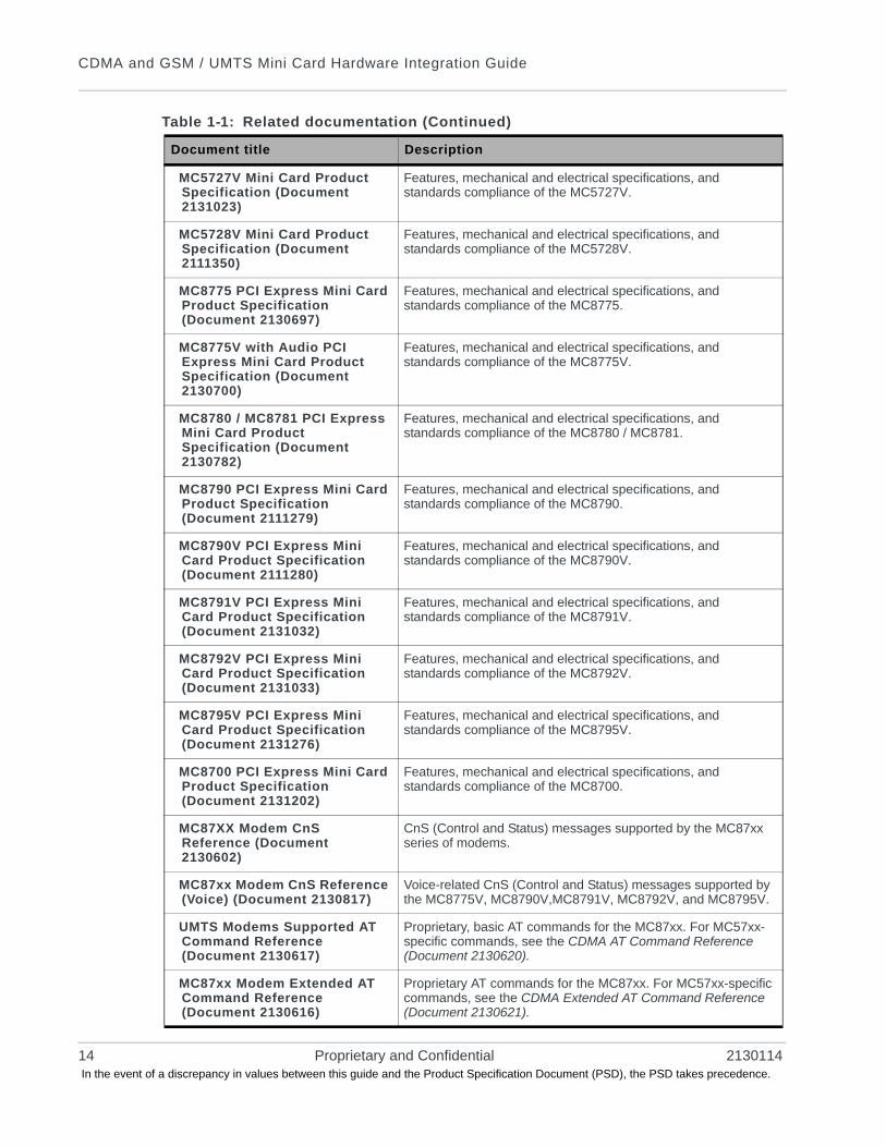
Table 1-1: Related documentation
Document title Description
AT Command Set for User Equipment (UE) (Release 6)
Standard AT commands for GSM / UMTS devices.Download this document (3GPP TS 27.007) from www.3gpp.org.
CDMA 1X Standard Technical requirements for CDMA systems, including details on sleep cycle index (SCI) values.Order this document, CDMA 2000 Series Release A (2000) (document # TIA/EIA/IS-2000 Series, Release A) from www.tiaonline.org.
CDMA CnS Reference (Document 2130754)
CnS (Control and Status) messages that are supported by the MC5725 / MC5725V / MC5727 / MC5727V / MC5728V.
CDMA AT Command Reference (Document 2130620)
Proprietary, basic AT commands for the MC5725 / MC5725V / MC5727 / MC5727V / MC5728V.For MC87xx-specific commands, see UMTS Modems Supported AT Command Reference (Document 2130617).
CDMA Extended AT Command Reference (Document 2130621)
Proprietary AT commands for the MC5725 / MC5725V / MC5727 / MC5727V / MC5728V.For MC87xx-specific commands, see MC87xx Modem Extended AT Command Reference (Document 2130616).
FCC Regulations - Part 15 - Radio Frequency Devices
This section of the FCC Code of Federal Regulations, Title 47 deals with radio frequency devices, including shielding requirements for embedded modules.Download this regulation from http://wireless.fcc.gov.
IEC-61000-4-2 level 3 Techniques for testing and measuring electrostatic discharge (ESD) immunity.Order this document from www.iec.ch.
MC5725 Mini Card Product Specification (Document 2130663)
Features, mechanical and electrical specifications, and standards compliance of the MC5725.
MC5725V Mini Card Product Specification (Document 2130671)
Features, mechanical and electrical specifications, and standards compliance of the MC5725V.
MC5727 Mini Card Product Specification (Document 2130958)
Features, mechanical and electrical specifications, and standards compliance of the MC5727.
Rev 1.14 Feb.10 Proprietary and Confidential 13 In the event of a discrepancy in values between this guide and the Product Specification Document (PSD), the PSD takes precedence.
CDMA and GSM / UMTS Mini Card Hardware Integration Guide
MC5727V Mini Card Product Specification (Document 2131023)
Features, mechanical and electrical specifications, and standards compliance of the MC5727V.
MC5728V Mini Card Product Specification (Document 2111350)
Features, mechanical and electrical specifications, and standards compliance of the MC5728V.
MC8775 PCI Express Mini Card Product Specification (Document 2130697)
Features, mechanical and electrical specifications, and standards compliance of the MC8775.
MC8775V with Audio PCI Express Mini Card Product Specification (Document 2130700)
Features, mechanical and electrical specifications, and standards compliance of the MC8775V.
MC8780 / MC8781 PCI Express Mini Card Product Specification (Document 2130782)
Features, mechanical and electrical specifications, and standards compliance of the MC8780 / MC8781.
MC8790 PCI Express Mini Card Product Specification (Document 2111279)
Features, mechanical and electrical specifications, and standards compliance of the MC8790.
MC8790V PCI Express Mini Card Product Specification (Document 2111280)
Features, mechanical and electrical specifications, and standards compliance of the MC8790V.
MC8791V PCI Express Mini Card Product Specification (Document 2131032)
Features, mechanical and electrical specifications, and standards compliance of the MC8791V.
MC8792V PCI Express Mini Card Product Specification (Document 2131033)
Features, mechanical and electrical specifications, and standards compliance of the MC8792V.
MC8795V PCI Express Mini Card Product Specification (Document 2131276)
Features, mechanical and electrical specifications, and standards compliance of the MC8795V.
MC8700 PCI Express Mini Card Product Specification (Document 2131202)
Features, mechanical and electrical specifications, and standards compliance of the MC8700.
MC87XX Modem CnS Reference (Document 2130602)
CnS (Control and Status) messages supported by the MC87xx series of modems.
MC87xx Modem CnS Reference (Voice) (Document 2130817)
Voice-related CnS (Control and Status) messages supported by the MC8775V, MC8790V,MC8791V, MC8792V, and MC8795V.
UMTS Modems Supported AT Command Reference (Document 2130617)
Proprietary, basic AT commands for the MC87xx. For MC57xx-specific commands, see the CDMA AT Command Reference (Document 2130620).
MC87xx Modem Extended AT Command Reference (Document 2130616)
Proprietary AT commands for the MC87xx. For MC57xx-specific commands, see the CDMA Extended AT Command Reference (Document 2130621).
Table 1-1: Related documentation (Continued)
Document title Description
14 Proprietary and Confidential 2130114 In the event of a discrepancy in values between this guide and the Product Specification Document (PSD), the PSD takes precedence.
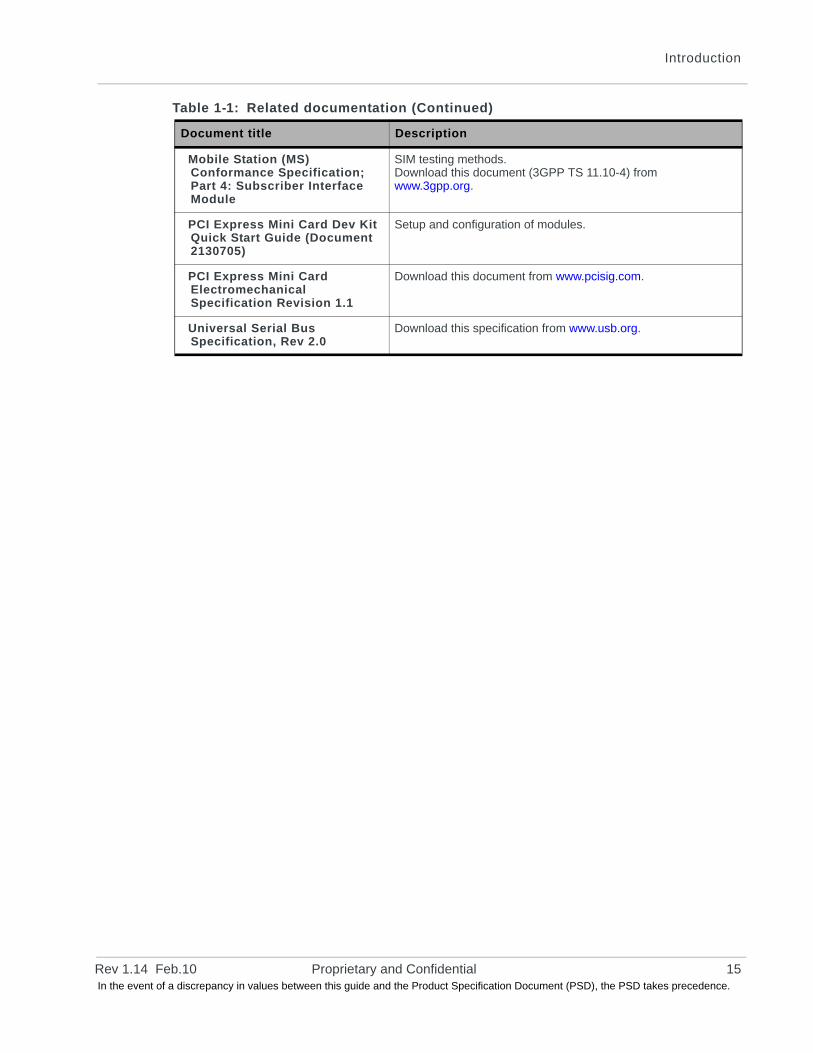
Introduction
Mobile Station (MS) Conformance Specification; Part 4: Subscriber Interface Module
SIM testing methods.Download this document (3GPP TS 11.10-4) from www.3gpp.org.
PCI Express Mini Card Dev Kit Quick Start Guide (Document 2130705)
Setup and configuration of modules.
PCI Express Mini Card Electromechanical Specification Revision 1.1
Download this document from www.pcisig.com.
Universal Serial Bus Specification, Rev 2.0
Download this specification from www.usb.org.
Table 1-1: Related documentation (Continued)
Document title Description
Rev 1.14 Feb.10 Proprietary and Confidential 15 In the event of a discrepancy in values between this guide and the Product Specification Document (PSD), the PSD takes precedence.
CDMA and GSM / UMTS Mini Card Hardware Integration Guide
16 Proprietary and Confidential 2130114 In the event of a discrepancy in values between this guide and the Product Specification Document (PSD), the PSD takes precedence.
Rev 1.14 In the event
22: Power Interface
Overview of operation
Note: This chapter contains information for CDMA (MC57xx) and GSM (MC87xx) modules.
Information that is unique to specific module types is clearly identified.
The module is designed to use a 3.3V (nominal) power supply, provided by the host. It is the host’s responsibility to provide safe and continuous power to the module at all times; the module does NOT have an independent power supply, or protection circuits to guard against electrical issues.
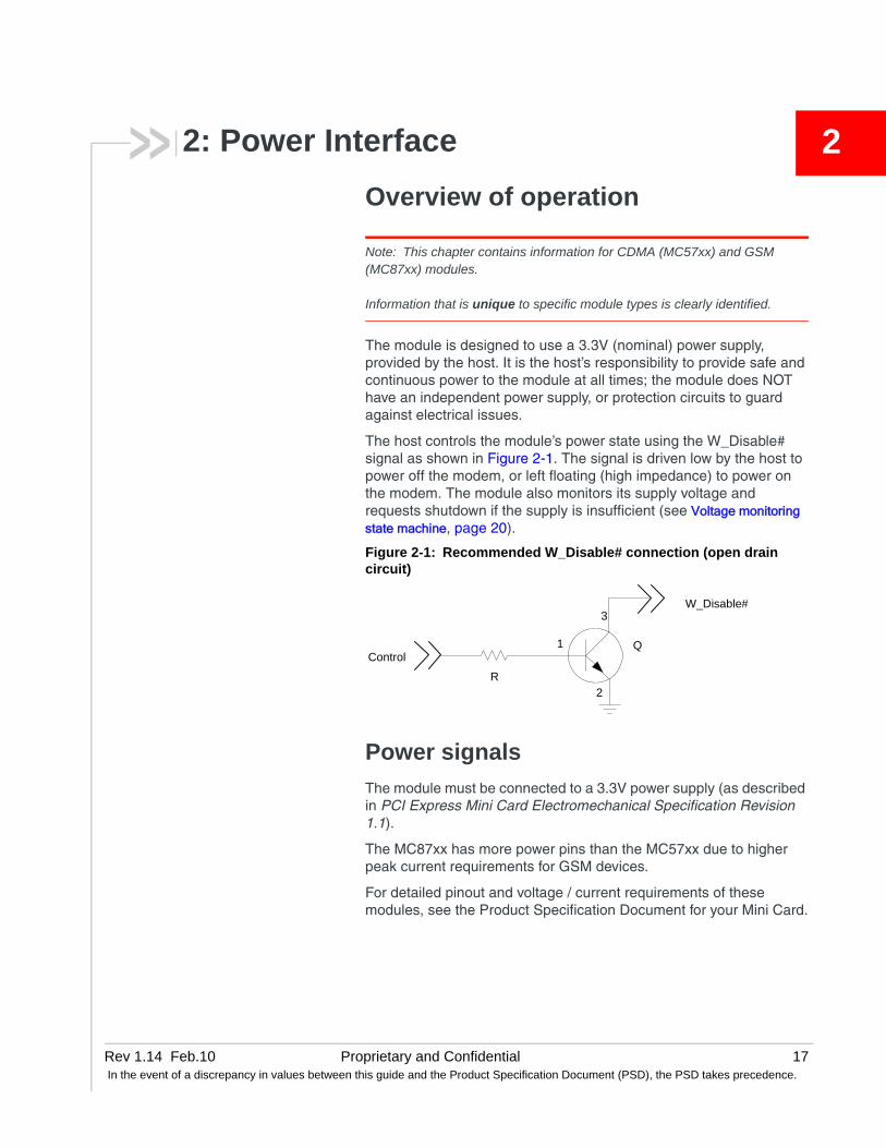
The host controls the module’s power state using the W_Disable# signal as shown in Figure 2-1. The signal is driven low by the host to power off the modem, or left floating (high impedance) to power on the modem. The module also monitors its supply voltage and requests shutdown if the supply is insufficient (see Voltage monitoring state machine, page 20).
Figure 2-1: Recommended W_Disable# connection (open drain circuit)
Power signals
The module must be connected to a 3.3V power supply (as described in PCI Express Mini Card Electromechanical Specification Revision 1.1).
The MC87xx has more power pins than the MC57xx due to higher peak current requirements for GSM devices.
For detailed pinout and voltage / current requirements of these modules, see the Product Specification Document for your Mini Card.
Control
R
W_Disable#
1
2
3
Q
Feb.10 Proprietary and Confidential 17of a discrepancy in values between this guide and the Product Specification Document (PSD), the PSD takes precedence.
CDMA and GSM / UMTS Mini Card Hardware Integration Guide
Note: The Product Specification Document’s pin connection table describes the internal structure of the module. For example, a Mini Card standard-compliant host platform provides +3.3Vaux on pin 24, but this pin is not connected internally on the MC8775V. Thus, the pin is flagged as ‘No connect’.
Electrostatic discharge (ESD)
You are responsible for ensuring that the host has adequate ESD protection on digital circuits and antenna ports:
• (Operational) RF port (antenna launch and RF connector): IEC-61000-4-2 — Level (Electrostatic Discharge Immunity Test)
• (Non-operational) Host connector interface: JESD22-A114-B +/- 1kV Human Body Model and JESD22-C101 +/- 125 V Charged Device Model
• MC5728V only: (Non-operational) Host connector interface: JESD22-A114-B +/- 125V Human Body Model and JESD22-C101 +/- 100 V Charged Device ModelMC5728V has placeholders for additional ESD devices, for cases where the device must, per customer requirements, meet the higher Human Body Model (+/-1kV) ESD rating.
Specific recommendations are provided where needed in this guide, however, the level of protection required depends on your application.
Note: ESD protection is highly recommended for the USIM connector at the point where the contacts are exposed, and for any other signals from the host interface that would be subjected to ESD by the user of the product.
Module power states
Note: The module unit defaults to the Normal state when VCC3.3 is first applied in the absence of W_Disable# control.
The module has four power states:
• DisconnectedNo power to the module.
• OffPower to the module, but the module is powered off.
• NormalThe module is active. Several modes are possible (Receive, Transmit, Sleep, Shutdown).
• Low power (“airplane mode”)The module is active, but RF is disabled.
State machines are implemented in the module to monitor the power supply and operating temperature.
18 Proprietary and Confidential 2130114 In the event of a discrepancy in values between this guide and the Product Specification Document (PSD), the PSD takes precedence.
Power Interface
Disconnected state
Note: The difference between the Discon-nected and Off states is that, in the Off state, the module is still connected to the power source and draws minimal current.
This state occurs when there is no power to the module — the host power source is disconnected from the module and all voltages associated with the module are at 0 V.
Whether the host device is also powered off depends on the power rail design. If the connection between the power rail and the module is controlled by the host, the host can stay powered on and cut the power to put the modem into the disconnected state. If the power rail is shared between the host device and the module, the host is powered off when the module is powered off.
Note: The module enters the Off state if W_Disable# is driven low and power (Vcc) is applied to the module, or if the module is in a powered state and W_Disable# is driven low for a module-dependent minimum period. See State change: Power off / on on page 23 for details.
Off state
In this state, the host is powered up and the module is powered down (but still connected to the power source).
The host keeps the module powered off by driving the W_Disable# signal low. In this state, the module draws minimal current.
For additional MC5728V information, see W_Disable# — Wireless disable on page 112.
Note: This is the default state when VCC3.3 is first applied in the absence of W_Disable# control.
Normal state
This is the active state of the module. In this state:
• The module is fully powered.
• The module is capable of placing / receiving calls or establishing data connections on the wireless network.
• The USB interface is fully active.
Low power mode
In this state, RF (both Rx and Tx) is disabled in the module, but the USB interface is still active. This low power mode ("airplane mode") is controlled by software commands through the host interface.
For instructions on using the commands, refer to AT Command Set for User Equipment (UE) (Release 6) (+CFUN=0 command), CDMA CnS Reference (Document 2130754) (CNS_RADIO_POWER [0x1075] command), or MC87XX Modem CnS Reference (Document 2130602) (Disable Modem command).
Rev 1.14 Feb.10 Proprietary and Confidential 19 In the event of a discrepancy in values between this guide and the Product Specification Document (PSD), the PSD takes precedence.
CDMA and GSM / UMTS Mini Card Hardware Integration Guide
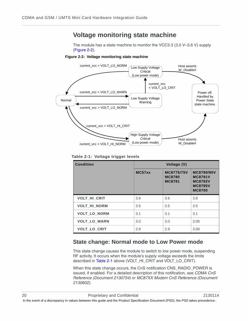
Voltage monitoring state machine
The module has a state machine to monitor the VCC3.3 (3.0 V–3.6 V) supply (Figure 2-2).
Figure 2-2: Voltage monitoring state machine
State change: Normal mode to Low Power mode
This state change causes the module to switch to low power mode, suspending RF activity. It occurs when the module’s supply voltage exceeds the limits described in Table 2-1 above (VOLT_HI_CRIT and VOLT_LO_CRIT).
When this state change occurs, the CnS notification CNS_RADIO_POWER is issued, if enabled. For a detailed description of this notification, see CDMA CnS Reference (Document 2130754) or MC87XX Modem CnS Reference (Document 2130602).
Table 2-1: Voltage trigger levels
Condition Voltage (V)
MC57xx MC8775/75VMC8780MC8781
MC8790/90VMC8791VMC8792VMC8795VMC8700
VOLT_HI_CRIT 3.6 3.6 3.8
VOLT_HI_NORM 3.5 3.5 3.5
VOLT_LO_NORM 3.1 3.1 3.1
VOLT_LO_WARN 3.0 3.0 3.05
VOLT_LO_CRIT 2.9 2.9 3.00
Normal
Low Supply VoltageCritical
(Low power mode)
Low Supply VoltageWarning
High Supply VoltageCritical
(Low power mode)
current_vcc > VOLT_LO_NORM
current_vcc < VOLT_LO_WARN
current_vcc > VOLT_LO_NORM
Host assertsW_Disable#
Host assertsW_Disable#
current_vcc< VOLT_LO_CRIT
current_vcc > VOLT_HI_CRIT
current_vcc < VOLT_HI_NORM
Power off.Handled byPower State
state machine.
20 Proprietary and Confidential 2130114 In the event of a discrepancy in values between this guide and the Product Specification Document (PSD), the PSD takes precedence.
Power Interface
State change: Low Power mode to Normal mode
This state change causes the module to switch to normal mode, resuming RF activity. It occurs when the module’s supply voltage returns from critical to normal limits as described in Table 2-1 on page 20 (VOLT_HI_NORM and VOLT_LO_NORM).
When this state change occurs, the CnS notification CNS_RADIO_POWER is issued, if enabled. For a detailed description of this notification, see CDMA CnS Reference (Document 2130754) or MC87XX Modem CnS Reference (Document 2130602).
Note: The module is still connected to the power source in this state, drawing minimal power.
State change: Power off / on
The module begins a shutdown sequence and powers off if it has been in a powered-on state for more than 10.5 seconds and the host device drives the W_Disable# signal low for:
• 50 ms (MC8775 / MC8775V)
• 500 ms (MC5725 / MC5725V / MC5727 / MC5727V / MC5728V / MC8780 / MC8781 / MC8790 / MC8790V / MC8791V / MC8792V / MC8795V / MC8700)
Note: The module ignores changes in the W_Disable# line for the first 10.5 seconds after it enters a powered-on state.
The module powers on when the host device leaves the W_Disable# signal floating (high impedance) as shown in Figure 2-1 on page 17.
Figure 2-2 on page 20 shows the transition from ‘Low Supply Voltage Critical’ or ‘High Supply Voltage Critical’ to ‘Power off’:
1. The module enters low power mode because it detects that the supply voltage level is critically low (VOLT_LO_CRIT) or critically high (VOLT_HI_CRIT).
2. The module sends a CnS notification (Return Radio Voltage—0x0009) to the host indicating that it is now in low power mode.
3. The host has the option, at this point, of driving W_Disable# low (forcing the module to power off) to prevent damage to the unit.
Rev 1.14 Feb.10 Proprietary and Confidential 21 In the event of a discrepancy in values between this guide and the Product Specification Document (PSD), the PSD takes precedence.
CDMA and GSM / UMTS Mini Card Hardware Integration Guide
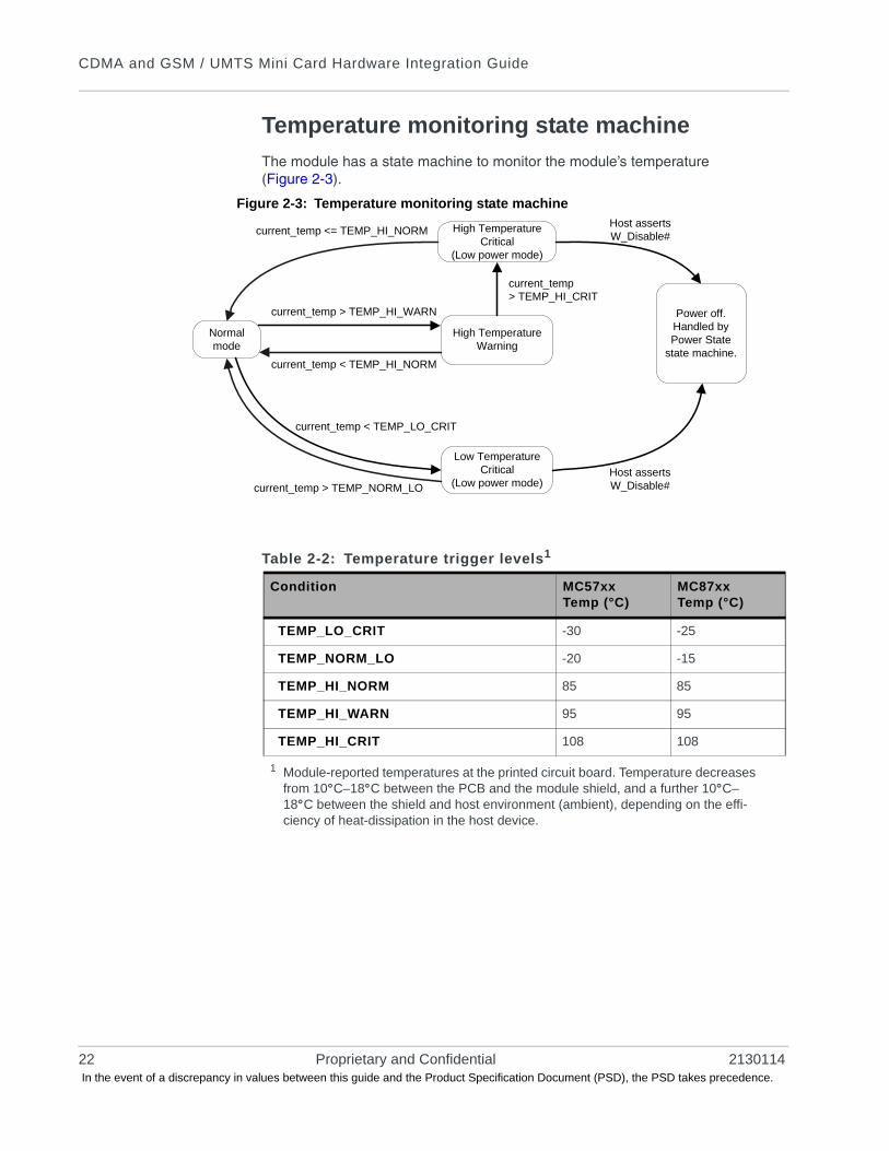
Temperature monitoring state machine
The module has a state machine to monitor the module’s temperature (Figure 2-3).
Figure 2-3: Temperature monitoring state machine
Table 2-2: Temperature trigger levels1
Condition MC57xxTemp (°C)
MC87xxTemp (°C)
TEMP_LO_CRIT -30 -25
TEMP_NORM_LO -20 -15
TEMP_HI_NORM 85 85
TEMP_HI_WARN 95 95
TEMP_HI_CRIT 108 108
1 Module-reported temperatures at the printed circuit board. Temperature decreases from 10°C–18°C between the PCB and the module shield, and a further 10°C–18°C between the shield and host environment (ambient), depending on the effi-ciency of heat-dissipation in the host device.
Normal mode
High Temperature Critical
(Low power mode)
High Temperature Warning
Low Temperature Critical
(Low power mode)
current_temp <= TEMP_HI_NORM
current_temp > TEMP_HI_WARN
current_temp < TEMP_HI_NORM
Host assertsW_Disable#
Host assertsW_Disable#
current_temp> TEMP_HI_CRIT
current_temp < TEMP_LO_CRIT
current_temp > TEMP_NORM_LO
Power off.Handled by Power State
state machine.
22 Proprietary and Confidential 2130114 In the event of a discrepancy in values between this guide and the Product Specification Document (PSD), the PSD takes precedence.
Power Interface
State change: Normal mode to Low Power mode
This state change causes the module to switch to low power mode, suspending RF activity. It occurs when the module temperature exceeds the limits described in Table 2-2 on page 22 (TEMP_HI_CRIT and TEMP_LO_CRIT).
When this state change occurs, the CnS notification CNS_RADIO_POWER is issued, if enabled. For a detailed description of this notification, see CDMA CnS Reference (Document 2130754) or MC87XX Modem CnS Reference (Document 2130602). As well, the MC57xx issues the CnS notification Modem Too Hot [0x4500] if it has to drop a call when shifting to low power mode.
State change: Low Power mode to Normal mode
This state change causes the module to switch to normal mode, resuming RF activity. It occurs when the module temperature returns from critical to normal limits as described in Table 2-2 on page 22 (TEMP_HI_NORM and TEMP_LO_NORM).
When this state change occurs, the CnS notification CNS_RADIO_POWER is issued, if enabled. For a detailed description of this notification, see CDMA CnS Reference (Document 2130754) or MC87XX Modem CnS Reference (Document 2130602).
State change: Power off / on
The module begins a shutdown sequence and powers off if it has been in a powered-on state for more than 10.5 seconds and the host device drives the W_Disable# signal low for:
• 50 ms (MC8775 / MC8775V)
• 500 ms (MC5725 / MC5725V / MC5727 / MC5727V / MC5728V / MC8780 / MC8781 / MC8790 / MC8790V / MC8791V / MC8792V / MC8795V / MC8700)
Note: The module ignores changes in the W_Disable# line for the first 10.5 seconds after it enters a powered-on state.
The module powers on when the host device leaves the W_Disable# signal floating (high impedance) as shown in Figure 2-1 on page 17.
Figure 2-3 shows the transition from ‘Low Temperature Critical’ or ‘High Temperature Critical’ to ‘Power off’.
1. The module enters low power mode because it detects that the operating temperature is critically low (TEMP_LO_CRIT) or critically high (TEMP_HI_CRIT).
2. The module sends a CnS notification (Return Radio Temperature—0x0008) to the host indicating that it is now in low power mode.
3. The host has the option, at this point, of driving W_Disable# low (forcing the module to power off) to prevent damage to the unit.
Rev 1.14 Feb.10 Proprietary and Confidential 23 In the event of a discrepancy in values between this guide and the Product Specification Document (PSD), the PSD takes precedence.
CDMA and GSM / UMTS Mini Card Hardware Integration Guide
Note: (MC57xx only) If the ambient temperature of the module exceeds 60 °C, the RF level is automatically lowered for max power transmission.
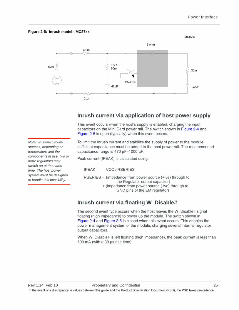
Inrush currents
Two power events can cause large inrush currents from the host supply to the module on the power pins:
• Application of the host’s power supply
• Host leaves W_Disable# floating (high impedance) to power up the module (as shown in Figure 2-1 on page 17).
Figure 2-4 and Figure 2-5 show the inrush models for the MC57xx and MC87xx. Application of the host’s power supply typically occurs when the switch is open; W_Disable# is left floating (high impedance) when the switch is closed.
Figure 2-4: Inrush model - MC57xx
REG
PWR (1,2,3,4,5)
ON/OFF (18)
Current
+3.3VDC
Power source
250m
LDO pass element
1 ohm typ
ESR80m
8.5m 2.8m 1.7m 2.2m
1uF
ESR20mESR
20m
38m
Cin2x 1uF
10m32m
Current ProbeMC57xx
Regulator input capacitor
Regulator output
capacitor
ESR + trace Z
60m
RF Cap4.7uF
EM board decoupling cap
Recommended host power rail capacitance = 470 µF - 1000 µF
Cin2x 1uF
ESR + trace Z
40m
EM board decoupling cap
15m
24 Proprietary and Confidential 2130114 In the event of a discrepancy in values between this guide and the Product Specification Document (PSD), the PSD takes precedence.
Power Interface
Figure 2-5: Inrush model - MC87xx
Inrush current via application of host power supply
This event occurs when the host’s supply is enabled, charging the input capacitors on the Mini Card power rail. The switch shown in Figure 2-4 and Figure 2-5 is open (typically) when this event occurs.
Note: In some circum-stances, depending on temperature and the components in use, two or more regulators may switch on at the same time. The host power system must be designed to handle this possibility.
To limit the inrush current and stabilize the supply of power to the module, sufficient capacitance must be added to the host power rail. The recommended capacitance range is 470 µF–1000 µF.
Peak current (IPEAK) is calculated using:
Inrush current via floating W_Disable#
The second event type occurs when the host leaves the W_Disable# signal floating (high impedance) to power up the module. The switch shown in Figure 2-4 and Figure 2-5 is closed when this event occurs. This enables the power management system of the module, charging several internal regulator output capacitors.
When W_Disable# is left floating (high impedance), the peak current is less than 500 mA (with a 30 µs rise time).
ON/OFF
50m
2 ohm
30m
0.1m
10uF
ESR50m
4.5m
47uF
MC87xx
IPEAK = VCC / RSERIES
RSERIES = (impedance from power source (+ive) through tothe Regulator output capacitor)
+ (impedance from power source (-ive) through toGND pins of the EM regulator)
Rev 1.14 Feb.10 Proprietary and Confidential 25 In the event of a discrepancy in values between this guide and the Product Specification Document (PSD), the PSD takes precedence.
CDMA and GSM / UMTS Mini Card Hardware Integration Guide
Timing requirements
Power ramp-up
During the first 0.5 seconds, as the internal voltage regulators are activated in sequence, several current transients of up to 500 mA with a 30 µs rise time may occur.
The supply voltage must remain within specified tolerances while this is occurring.
Power-up timing
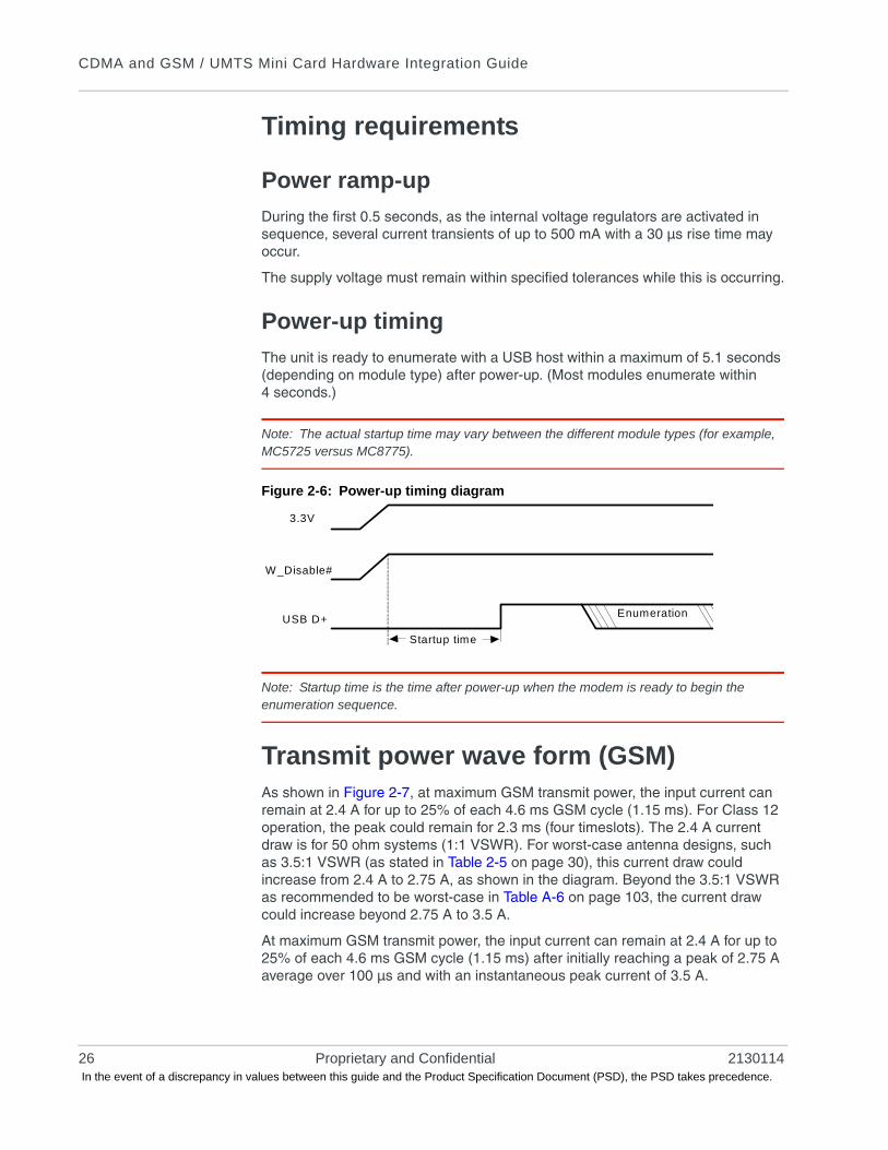
The unit is ready to enumerate with a USB host within a maximum of 5.1 seconds (depending on module type) after power-up. (Most modules enumerate within 4 seconds.)
Note: The actual startup time may vary between the different module types (for example, MC5725 versus MC8775).
Figure 2-6: Power-up timing diagram
Note: Startup time is the time after power-up when the modem is ready to begin the enumeration sequence.
Transmit power wave form (GSM)As shown in Figure 2-7, at maximum GSM transmit power, the input current can remain at 2.4 A for up to 25% of each 4.6 ms GSM cycle (1.15 ms). For Class 12 operation, the peak could remain for 2.3 ms (four timeslots). The 2.4 A current draw is for 50 ohm systems (1:1 VSWR). For worst-case antenna designs, such as 3.5:1 VSWR (as stated in Table 2-5 on page 30), this current draw could increase from 2.4 A to 2.75 A, as shown in the diagram. Beyond the 3.5:1 VSWR as recommended to be worst-case in Table A-6 on page 103, the current draw could increase beyond 2.75 A to 3.5 A.
At maximum GSM transmit power, the input current can remain at 2.4 A for up to 25% of each 4.6 ms GSM cycle (1.15 ms) after initially reaching a peak of 2.75 A average over 100 µs and with an instantaneous peak current of 3.5 A.
Enumeration
3.3V
W_Disable#
USB D+
Startup time
26 Proprietary and Confidential 2130114 In the event of a discrepancy in values between this guide and the Product Specification Document (PSD), the PSD takes precedence.
Power Interface
Figure 2-7: GSM transmit power wave form
Current consumptionCurrent consumption depends on the module’s operating mode at any given time.
This section describes:
• Current consumption for both module types (MC57xx and MC87xx)
• Operating modes
Current consumption overview
Note: Values in this guide are taken from the appro-priate product specifi-cation documents (PSDs) (listed in Related documents, page 13) — in the case of a discrepancy between this document and the relevant PSD, use the value listed in the PSD.
Electrical requirements and current specifications are listed in Table 2-3 on page 28 (MC57xx), Table 2-4 on page 28 (MC8775/MC8775V), Table 2-5 on page 30 (MC8780/MC8781), Table 2-6 on page 31 (MC8790/MC8790V/MC8791V/MC8792V/MC8795V), and Table 2-8 on page 33 (MC8700). These specifications identify minimum, typical, and maximum current drain for each operating mode (while in the Normal state):
• Transmit
• Receive
• Sleep
• Deep sleep
• Shutdown
The current consumption values in these tables were measured using a supply voltage of 3.3 V. The device’s supply voltage is 3.0–3.6 V with a typical voltage of 3.3 V.
2.4
0.15
Current(A)
2.75A peak
2.75
25 µs1.15 ms
4.6 ms
3.5:1 VSWR = 2.75A
1:1 VSWR = 2.40A
Rev 1.14 Feb.10 Proprietary and Confidential 27 In the event of a discrepancy in values between this guide and the Product Specification Document (PSD), the PSD takes precedence.
CDMA and GSM / UMTS Mini Card Hardware Integration Guide
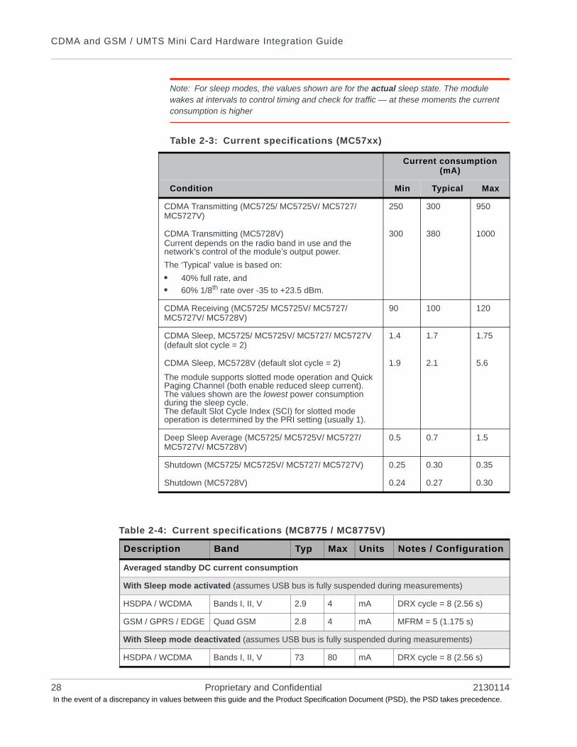
Note: For sleep modes, the values shown are for the actual sleep state. The module wakes at intervals to control timing and check for traffic — at these moments the current consumption is higher
Table 2-3: Current specifications (MC57xx)
Current consumption (mA)
Condition Min Typical Max
CDMA Transmitting (MC5725/ MC5725V/ MC5727/ MC5727V)
250 300 950
CDMA Transmitting (MC5728V)Current depends on the radio band in use and the network’s control of the module’s output power.
The ‘Typical’ value is based on:
• 40% full rate, and
• 60% 1/8th rate over -35 to +23.5 dBm.
300 380 1000
CDMA Receiving (MC5725/ MC5725V/ MC5727/ MC5727V/ MC5728V)
90 100 120
CDMA Sleep, MC5725/ MC5725V/ MC5727/ MC5727V (default slot cycle = 2)
1.4 1.7 1.75
CDMA Sleep, MC5728V (default slot cycle = 2)
The module supports slotted mode operation and Quick Paging Channel (both enable reduced sleep current). The values shown are the lowest power consumption during the sleep cycle.The default Slot Cycle Index (SCI) for slotted mode operation is determined by the PRI setting (usually 1).
1.9 2.1 5.6
Deep Sleep Average (MC5725/ MC5725V/ MC5727/ MC5727V/ MC5728V)
0.5 0.7 1.5
Shutdown (MC5725/ MC5725V/ MC5727/ MC5727V) 0.25 0.30 0.35
Shutdown (MC5728V) 0.24 0.27 0.30
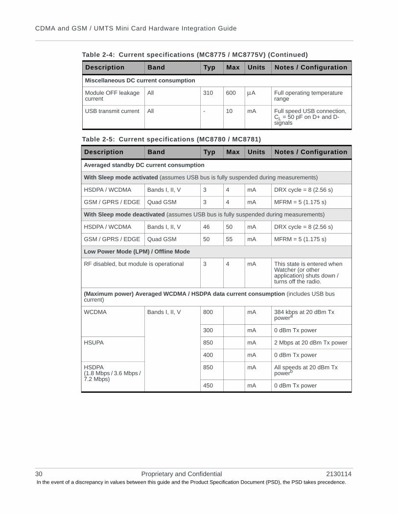
Table 2-4: Current specifications (MC8775 / MC8775V)
Description Band Typ Max Units Notes / Configuration
Averaged standby DC current consumption
With Sleep mode activated (assumes USB bus is fully suspended during measurements)
HSDPA / WCDMA Bands I, II, V 2.9 4 mA DRX cycle = 8 (2.56 s)
GSM / GPRS / EDGE Quad GSM 2.8 4 mA MFRM = 5 (1.175 s)
With Sleep mode deactivated (assumes USB bus is fully suspended during measurements)
HSDPA / WCDMA Bands I, II, V 73 80 mA DRX cycle = 8 (2.56 s)
28 Proprietary and Confidential 2130114 In the event of a discrepancy in values between this guide and the Product Specification Document (PSD), the PSD takes precedence.
Power Interface
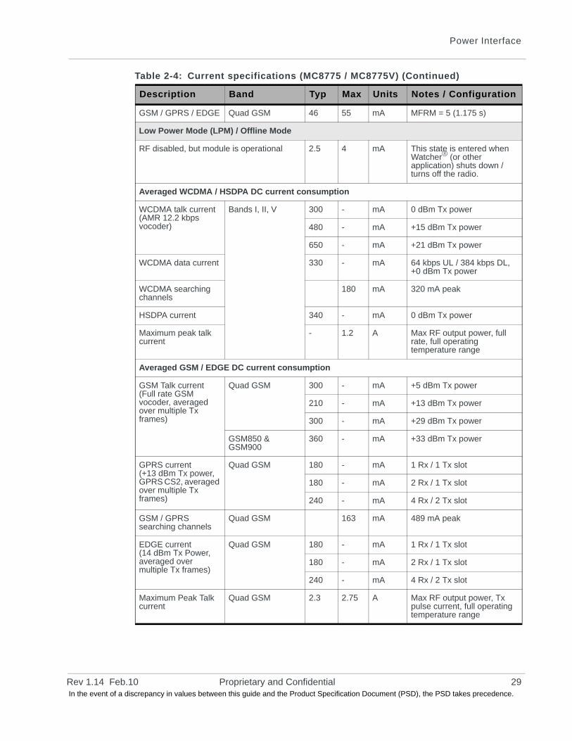
GSM / GPRS / EDGE Quad GSM 46 55 mA MFRM = 5 (1.175 s)
Low Power Mode (LPM) / Offline Mode
RF disabled, but module is operational 2.5 4 mA This state is entered when Watcher® (or other application) shuts down / turns off the radio.
Averaged WCDMA / HSDPA DC current consumption
WCDMA talk current (AMR 12.2 kbps vocoder)
Bands I, II, V 300 - mA 0 dBm Tx power
480 - mA +15 dBm Tx power
650 - mA +21 dBm Tx power
WCDMA data current 330 - mA 64 kbps UL / 384 kbps DL, +0 dBm Tx power
WCDMA searching channels
180 mA 320 mA peak
HSDPA current 340 - mA 0 dBm Tx power
Maximum peak talk current
- 1.2 A Max RF output power, full rate, full operating temperature range
Averaged GSM / EDGE DC current consumption
GSM Talk current (Full rate GSM vocoder, averaged over multiple Tx frames)
Quad GSM 300 - mA +5 dBm Tx power
210 - mA +13 dBm Tx power
300 - mA +29 dBm Tx power
GSM850 & GSM900
360 - mA +33 dBm Tx power
GPRS current (+13 dBm Tx power, GPRS CS2, averaged over multiple Tx frames)
Quad GSM 180 - mA 1 Rx / 1 Tx slot
180 - mA 2 Rx / 1 Tx slot
240 - mA 4 Rx / 2 Tx slot
GSM / GPRS searching channels
Quad GSM 163 mA 489 mA peak
EDGE current (14 dBm Tx Power, averaged over multiple Tx frames)
Quad GSM 180 - mA 1 Rx / 1 Tx slot
180 - mA 2 Rx / 1 Tx slot
240 - mA 4 Rx / 2 Tx slot
Maximum Peak Talk current
Quad GSM 2.3 2.75 A Max RF output power, Tx pulse current, full operating temperature range
Table 2-4: Current specifications (MC8775 / MC8775V) (Continued)
Description Band Typ Max Units Notes / Configuration
Rev 1.14 Feb.10 Proprietary and Confidential 29 In the event of a discrepancy in values between this guide and the Product Specification Document (PSD), the PSD takes precedence.
CDMA and GSM / UMTS Mini Card Hardware Integration Guide
Miscellaneous DC current consumption
Module OFF leakage current
All 310 600 A Full operating temperature range
USB transmit current All - 10 mA Full speed USB connection, CL = 50 pF on D+ and D- signals
Table 2-5: Current specifications (MC8780 / MC8781)
Description Band Typ Max Units Notes / Configuration
Averaged standby DC current consumption
With Sleep mode activated (assumes USB bus is fully suspended during measurements)
HSDPA / WCDMA Bands I, II, V 3 4 mA DRX cycle = 8 (2.56 s)
GSM / GPRS / EDGE Quad GSM 3 4 mA MFRM = 5 (1.175 s)
With Sleep mode deactivated (assumes USB bus is fully suspended during measurements)
HSDPA / WCDMA Bands I, II, V 46 50 mA DRX cycle = 8 (2.56 s)
GSM / GPRS / EDGE Quad GSM 50 55 mA MFRM = 5 (1.175 s)
Low Power Mode (LPM) / Offline Mode
RF disabled, but module is operational 3 4 mA This state is entered when Watcher (or other application) shuts down / turns off the radio.
(Maximum power) Averaged WCDMA / HSDPA data current consumption (includes USB bus current)
WCDMA Bands I, II, V 800 mA 384 kbps at 20 dBm Tx powera
300 mA 0 dBm Tx power
HSUPA 850 mA 2 Mbps at 20 dBm Tx power
400 mA 0 dBm Tx power
HSDPA(1.8 Mbps / 3.6 Mbps / 7.2 Mbps)
850 mA All speeds at 20 dBm Tx powerb
450 mA 0 dBm Tx power
Table 2-4: Current specifications (MC8775 / MC8775V) (Continued)
Description Band Typ Max Units Notes / Configuration
30 Proprietary and Confidential 2130114 In the event of a discrepancy in values between this guide and the Product Specification Document (PSD), the PSD takes precedence.
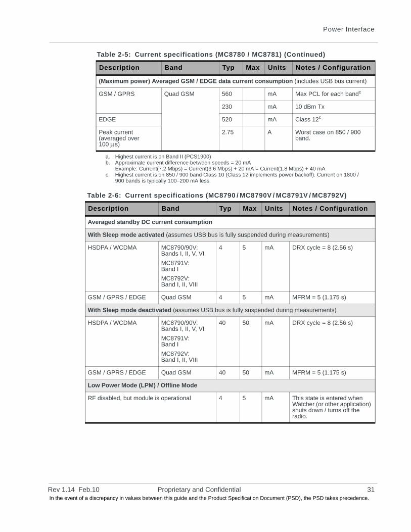
Power Interface
(Maximum power) Averaged GSM / EDGE data current consumption (includes USB bus current)
GSM / GPRS Quad GSM 560 mA Max PCL for each bandc
230 mA 10 dBm Tx
EDGE 520 mA Class 12c
Peak current (averaged over 100 s)
2.75 A Worst case on 850 / 900 band.
a. Highest current is on Band II (PCS1900)b. Approximate current difference between speeds = 20 mA
Example: Current(7.2 Mbps) = Current(3.6 Mbps) + 20 mA = Current(1.8 Mbps) + 40 mAc. Highest current is on 850 / 900 band Class 10 (Class 12 implements power backoff). Current on 1800 /
900 bands is typically 100–200 mA less.
Table 2-6: Current specifications (MC8790 / MC8790V / MC8791V / MC8792V)
Description Band Typ Max Units Notes / Configuration
Averaged standby DC current consumption
With Sleep mode activated (assumes USB bus is fully suspended during measurements)
HSDPA / WCDMA MC8790/90V: Bands I, II, V, VI
MC8791V:Band I
MC8792V:Band I, II, VIII
4 5 mA DRX cycle = 8 (2.56 s)
GSM / GPRS / EDGE Quad GSM 4 5 mA MFRM = 5 (1.175 s)
With Sleep mode deactivated (assumes USB bus is fully suspended during measurements)
HSDPA / WCDMA MC8790/90V: Bands I, II, V, VI
MC8791V:Band I
MC8792V:Band I, II, VIII
40 50 mA DRX cycle = 8 (2.56 s)
GSM / GPRS / EDGE Quad GSM 40 50 mA MFRM = 5 (1.175 s)
Low Power Mode (LPM) / Offline Mode
RF disabled, but module is operational 4 5 mA This state is entered when Watcher (or other application) shuts down / turns off the radio.
Table 2-5: Current specifications (MC8780 / MC8781) (Continued)
Description Band Typ Max Units Notes / Configuration
Rev 1.14 Feb.10 Proprietary and Confidential 31 In the event of a discrepancy in values between this guide and the Product Specification Document (PSD), the PSD takes precedence.
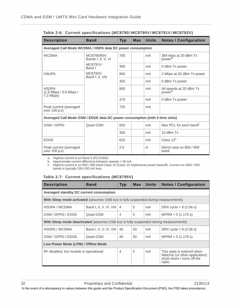
CDMA and GSM / UMTS Mini Card Hardware Integration Guide
Averaged Call Mode WCDMA / HSPA data DC power consumption
WCDMA MC8790/90V: Bands I, II, V, VI
MC8791V:Band I
MC8792V:Band I, II, VIII
700 mA 384 kbps at 20 dBm Tx powera
300 mA 0 dBm Tx power
HSUPA 800 mA 2 Mbps at 20 dBm Tx power
350 mA 0 dBm Tx power
HSDPA(1.8 Mbps / 3.6 Mbps / 7.2 Mbps)
800 mA All speeds at 20 dBm Tx powerb
370 mA 0 dBm Tx power
Peak current (averaged over 100 s)
720 mA
Averaged Call Mode GSM / EDGE data DC power consumption (with 4 time slots)
GSM / GPRS Quad GSM 650 mA Max PCL for each bandc
300 mA 10 dBm Tx
EDGE 620 mA Class 12c
Peak current (averaged over 100 s)
2.6 A Worst case on 850 / 900 band.
a. Highest current is on Band II (PCS1900)b. Approximate current difference between speeds = 30 mAc. Highest current is on 850 / 900 band Class 10 (Class 12 implements power backoff). Current on 1800 / 900
bands is typically 100–200 mA less.
Table 2-7: Current specifications (MC8795V)
Description Band Typ Max Units Notes / Configuration
Averaged standby DC current consumption
With Sleep mode activated (assumes USB bus is fully suspended during measurements)
HSDPA / WCDMA Band I, II, V, VI, VIII 4 5 mA DRX cycle = 8 (2.56 s)
GSM / GPRS / EDGE Quad GSM 4 5 mA MFRM = 5 (1.175 s)
With Sleep mode deactivated (assumes USB bus is fully suspended during measurements)
HSDPA / WCDMA Band I, II, V, VI, VIII 40 50 mA DRX cycle = 8 (2.56 s)
GSM / GPRS / EDGE Quad GSM 40 50 mA MFRM = 5 (1.175 s)
Low Power Mode (LPM) / Offline Mode
RF disabled, but module is operational 4 5 mA This state is entered when Watcher (or other application) shuts down / turns off the radio.
Table 2-6: Current specifications (MC8790 / MC8790V / MC8791V / MC8792V)
Description Band Typ Max Units Notes / Configuration
32 Proprietary and Confidential 2130114 In the event of a discrepancy in values between this guide and the Product Specification Document (PSD), the PSD takes precedence.
Power Interface
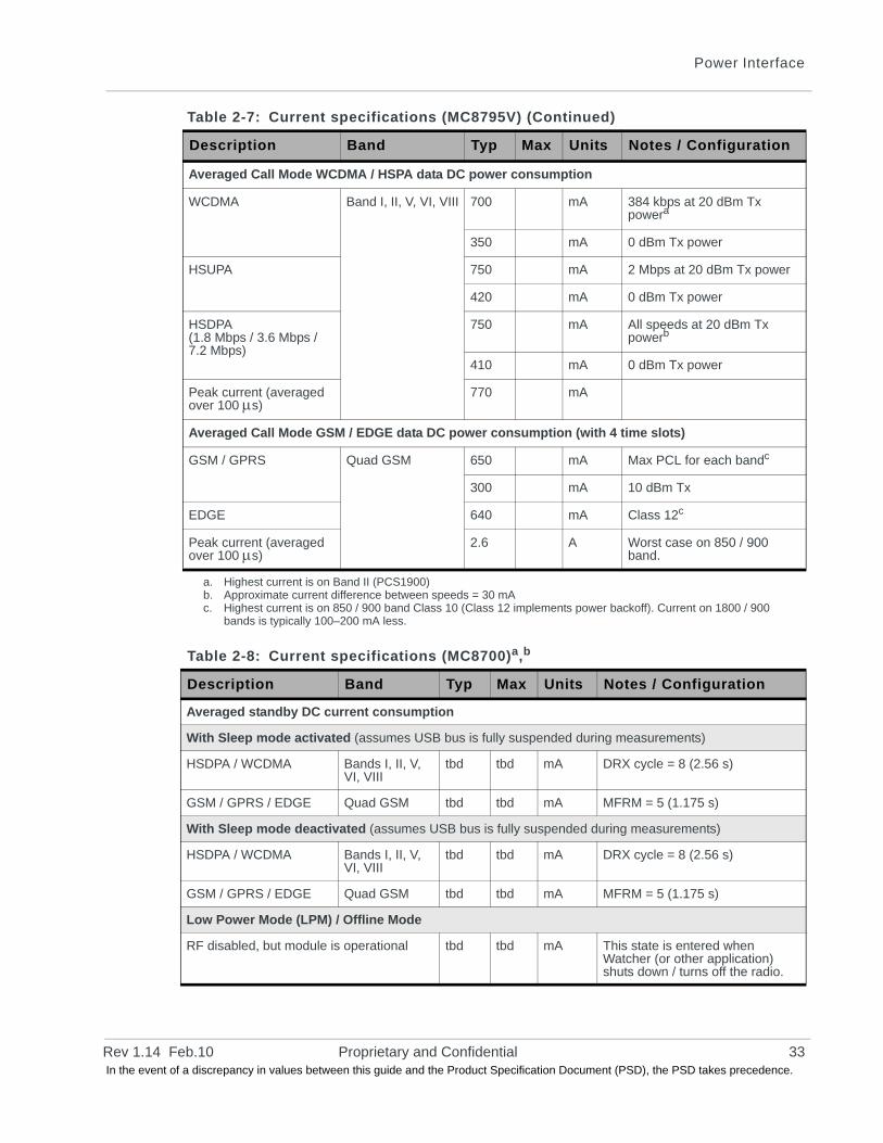
Averaged Call Mode WCDMA / HSPA data DC power consumption
WCDMA Band I, II, V, VI, VIII 700 mA 384 kbps at 20 dBm Tx powera
350 mA 0 dBm Tx power
HSUPA 750 mA 2 Mbps at 20 dBm Tx power
420 mA 0 dBm Tx power
HSDPA(1.8 Mbps / 3.6 Mbps / 7.2 Mbps)
750 mA All speeds at 20 dBm Tx powerb
410 mA 0 dBm Tx power
Peak current (averaged over 100 s)
770 mA
Averaged Call Mode GSM / EDGE data DC power consumption (with 4 time slots)
GSM / GPRS Quad GSM 650 mA Max PCL for each bandc
300 mA 10 dBm Tx
EDGE 640 mA Class 12c
Peak current (averaged over 100 s)
2.6 A Worst case on 850 / 900 band.
a. Highest current is on Band II (PCS1900)b. Approximate current difference between speeds = 30 mAc. Highest current is on 850 / 900 band Class 10 (Class 12 implements power backoff). Current on 1800 / 900
bands is typically 100–200 mA less.
Table 2-8: Current specifications (MC8700)a,b
Description Band Typ Max Units Notes / Configuration
Averaged standby DC current consumption
With Sleep mode activated (assumes USB bus is fully suspended during measurements)
HSDPA / WCDMA Bands I, II, V, VI, VIII
tbd tbd mA DRX cycle = 8 (2.56 s)
GSM / GPRS / EDGE Quad GSM tbd tbd mA MFRM = 5 (1.175 s)
With Sleep mode deactivated (assumes USB bus is fully suspended during measurements)
HSDPA / WCDMA Bands I, II, V, VI, VIII
tbd tbd mA DRX cycle = 8 (2.56 s)
GSM / GPRS / EDGE Quad GSM tbd tbd mA MFRM = 5 (1.175 s)
Low Power Mode (LPM) / Offline Mode
RF disabled, but module is operational tbd tbd mA This state is entered when Watcher (or other application) shuts down / turns off the radio.
Table 2-7: Current specifications (MC8795V) (Continued)
Description Band Typ Max Units Notes / Configuration
Rev 1.14 Feb.10 Proprietary and Confidential 33 In the event of a discrepancy in values between this guide and the Product Specification Document (PSD), the PSD takes precedence.
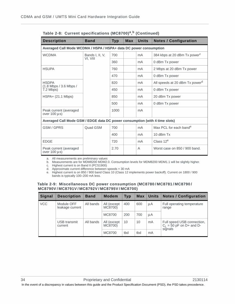
CDMA and GSM / UMTS Mini Card Hardware Integration Guide
Averaged Call Mode WCDMA / HSPA / HSPA+ data DC power consumption
WCDMA Bands I, II, V, VI, VIII
700 mA 384 kbps at 20 dBm Tx powerc
360 mA 0 dBm Tx power
HSUPA 760 mA 2 Mbps at 20 dBm Tx power
470 mA 0 dBm Tx power
HSDPA(1.8 Mbps / 3.6 Mbps / 7.2 Mbps)
820 mA All speeds at 20 dBm Tx powerd
450 mA 0 dBm Tx power
HSPA+ (21.1 Mbps) 850 mA 20 dBm Tx power
500 mA 0 dBm Tx power
Peak current (averaged over 100 s)
1000 mA
Averaged Call Mode GSM / EDGE data DC power consumption (with 4 time slots)
GSM / GPRS Quad GSM 700 mA Max PCL for each bande
400 mA 10 dBm Tx
EDGE 720 mA Class 12e
Peak current (averaged over 100 s)
2.70 A Worst case on 850 / 900 band.
a. All measurements are preliminary valuesb. Measurements are for MDM8200 MDM2.0. Consumption levels for MDM8200 MDM1.1 will be slightly higher.c. Highest current is on Band II (PCS1900)d. Approximate current difference between speeds = 30 mAe. Highest current is on 850 / 900 band Class 10 (Class 12 implements power backoff). Current on 1800 / 900
bands is typically 100–200 mA less.
Table 2-9: Miscellaneous DC power consumption (MC8780 / MC8781 / MC8790 /MC8790V / MC8791V / MC8792V / MC8795V / MC8700)
Signal Description Band Modem Typ Max Units Notes / Configuration
VCC Module OFF leakage current
All bands All (except MC8700)
400 600 A Full operating temperature range
MC8700 200 700 A
USB transmit current
All bands All (except MC8700)
10 10 mA Full speed USB connection, CL = 50 pF on D+ and D- signals
MC8700 tbd tbd mA
Table 2-8: Current specifications (MC8700)a,b (Continued)
Description Band Typ Max Units Notes / Configuration
34 Proprietary and Confidential 2130114 In the event of a discrepancy in values between this guide and the Product Specification Document (PSD), the PSD takes precedence.
Power Interface
Modes
Transmit and Receive modes
Current consumption in transmit or receive mode (in a call or data connection) is affected by several factors, such as:
• Radio band being used
• Transmit power
• Receive gain settings
• Data rate
• Number of active Transmit time slots (for transmit mode)
Sleep mode
Sleep mode is the normal state of the module between calls or data connections. In this reduced power mode, the module cycles between wake (polling the network) and sleep, at an interval determined by the network provider.
Deep sleep
Deep sleep mode is a reduced power, out-of-network-coverage mode, that the module enters when it cannot acquire network service after several minutes.
The module then exits deep sleep periodically to try to acquire service, and if successful, attempts to register.
Shutdown mode
While in shutdown mode, the module is powered off, but still draws a minimal current from the host power supply.
SED (Smart Error Detection)(MC87xx only)
The MC87xx modem uses a form of SED to track recurrent premature modem resets. In such cases, the modem automatically forces a pause in boot-and-hold mode at power-on to accept an expected firmware download to resolve the problem.
The SED process is implemented as follows:
• The modem tracks consecutive resets of the modem within 30 seconds of power-on.
• After a third consecutive reset occurs, the modem automatically waits up to 30 seconds in boot-and-hold mode, waiting for a firmware download to resolve the power-cycle problem.
• After 30 seconds (if no firmware download begins), the modem continues to power-on.
• If the modem resets again within 30 seconds of power-on, the modem again waits in boot-and-hold mode.
Rev 1.14 Feb.10 Proprietary and Confidential 35 In the event of a discrepancy in values between this guide and the Product Specification Document (PSD), the PSD takes precedence.
CDMA and GSM / UMTS Mini Card Hardware Integration Guide
This process continues until the unexpected power-cycle issue is resolved—either a firmware download occurs, or the modem doesn’t reset spontaneously within 30 seconds of power-on.
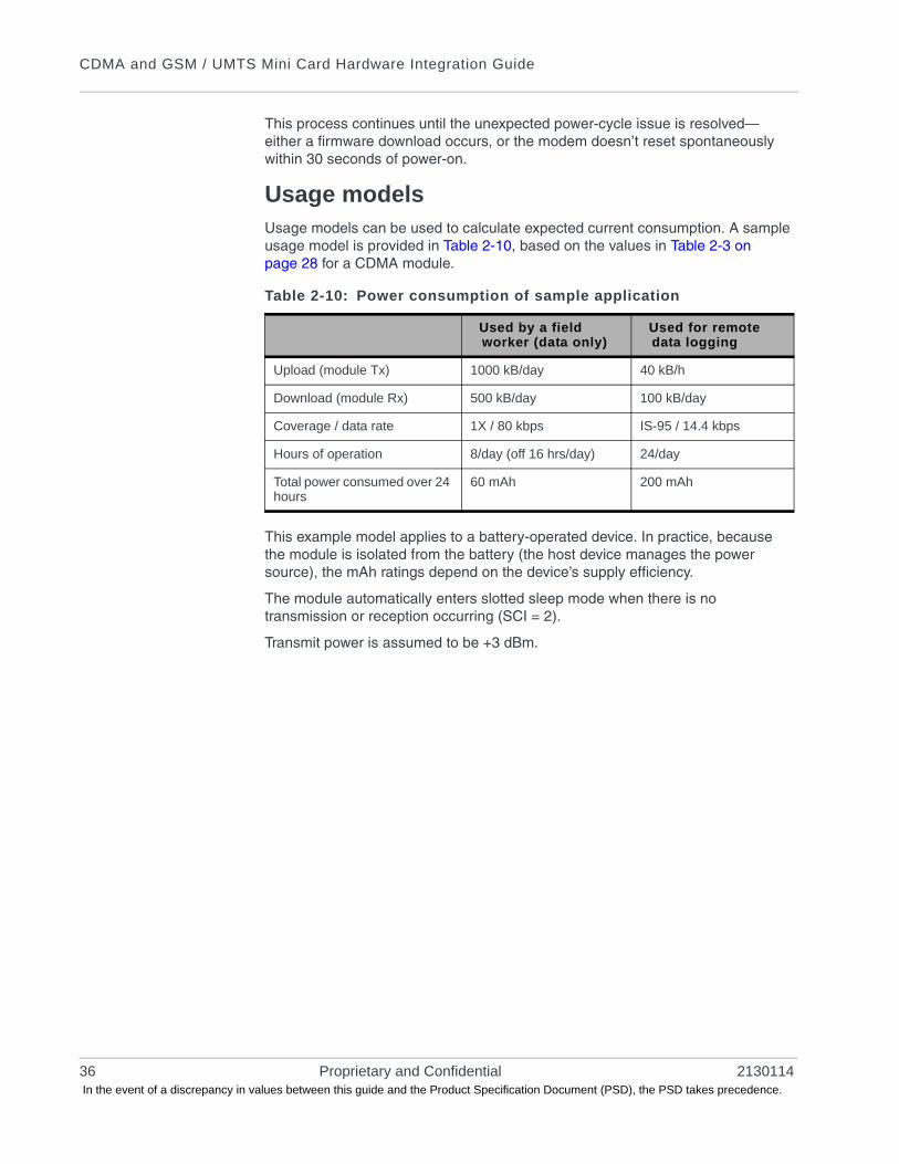
Usage modelsUsage models can be used to calculate expected current consumption. A sample usage model is provided in Table 2-10, based on the values in Table 2-3 on page 28 for a CDMA module.
This example model applies to a battery-operated device. In practice, because the module is isolated from the battery (the host device manages the power source), the mAh ratings depend on the device’s supply efficiency.
The module automatically enters slotted sleep mode when there is no transmission or reception occurring (SCI = 2).
Transmit power is assumed to be +3 dBm.
Table 2-10: Power consumption of sample application
Used by a field worker (data only)
Used for remote data logging
Upload (module Tx) 1000 kB/day 40 kB/h
Download (module Rx) 500 kB/day 100 kB/day
Coverage / data rate 1X / 80 kbps IS-95 / 14.4 kbps
Hours of operation 8/day (off 16 hrs/day) 24/day
Total power consumed over 24 hours
60 mAh 200 mAh
36 Proprietary and Confidential 2130114 In the event of a discrepancy in values between this guide and the Product Specification Document (PSD), the PSD takes precedence.
Rev 1.14 In the event
Product
MC8775MC8775VMC8780MC8781MC8790MC8790VMC8791VMC8792VMC8795VMC8700
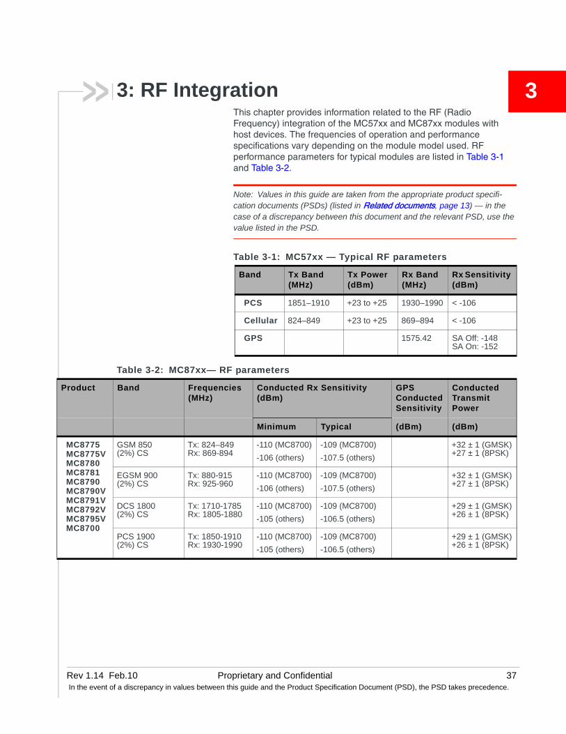
33: RF IntegrationThis chapter provides information related to the RF (Radio Frequency) integration of the MC57xx and MC87xx modules with host devices. The frequencies of operation and performance specifications vary depending on the module model used. RF performance parameters for typical modules are listed in Table 3-1 and Table 3-2.
Note: Values in this guide are taken from the appropriate product specifi-cation documents (PSDs) (listed in Related documents, page 13) — in the case of a discrepancy between this document and the relevant PSD, use the value listed in the PSD.
Table 3-1: MC57xx — Typical RF parameters
Band Tx Band (MHz)
Tx Power (dBm)
Rx Band (MHz)
Rx Sensitivity (dBm)
PCS 1851–1910 +23 to +25 1930–1990 < -106
Cellular 824–849 +23 to +25 869–894 < -106
GPS 1575.42 SA Off: -148SA On: -152
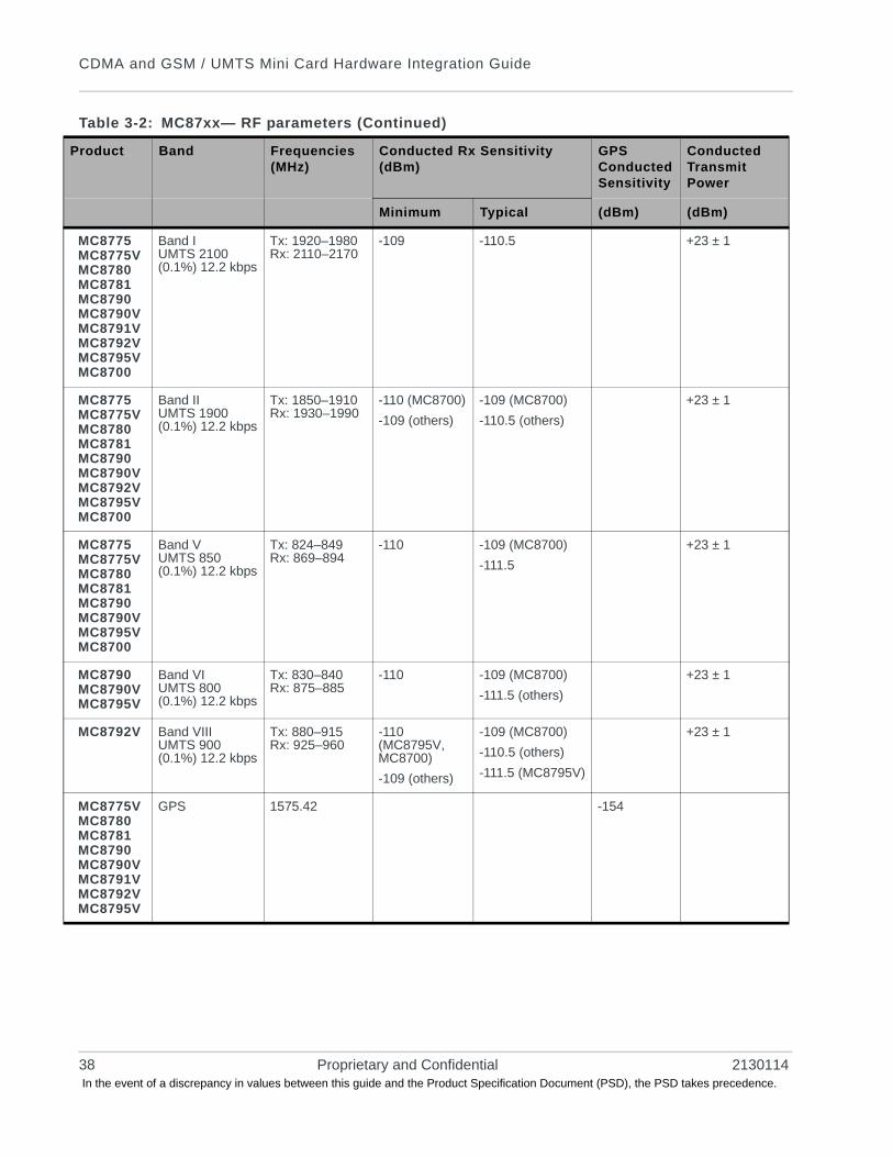
Table 3-2: MC87xx— RF parameters
Band Frequencies (MHz)
Conducted Rx Sensitivity (dBm)
GPS Conducted Sensitivity
Conducted Transmit Power
Minimum Typical (dBm) (dBm)
GSM 850(2%) CS
Tx: 824–849Rx: 869-894
-110 (MC8700)
-106 (others)
-109 (MC8700)
-107.5 (others)
+32 ± 1 (GMSK)+27 ± 1 (8PSK)
EGSM 900(2%) CS
Tx: 880-915Rx: 925-960
-110 (MC8700)
-106 (others)
-109 (MC8700)
-107.5 (others)
+32 ± 1 (GMSK)+27 ± 1 (8PSK)
DCS 1800(2%) CS
Tx: 1710-1785Rx: 1805-1880
-110 (MC8700)
-105 (others)
-109 (MC8700)
-106.5 (others)
+29 ± 1 (GMSK)+26 ± 1 (8PSK)
PCS 1900(2%) CS
Tx: 1850-1910Rx: 1930-1990
-110 (MC8700)
-105 (others)
-109 (MC8700)
-106.5 (others)
+29 ± 1 (GMSK)+26 ± 1 (8PSK)
Feb.10 Proprietary and Confidential 37of a discrepancy in values between this guide and the Product Specification Document (PSD), the PSD takes precedence.
CDMA and GSM / UMTS Mini Card Hardware Integration Guide
MC8775MC8775VMC8780MC8781MC8790MC8790VMC8791VMC8792VMC8795VMC8700
Band IUMTS 2100(0.1%) 12.2 kbps
Tx: 1920–1980Rx: 2110–2170
-109 -110.5 +23 ± 1
MC8775MC8775VMC8780MC8781MC8790MC8790VMC8792VMC8795VMC8700
Band IIUMTS 1900(0.1%) 12.2 kbps
Tx: 1850–1910Rx: 1930–1990
-110 (MC8700)
-109 (others)
-109 (MC8700)
-110.5 (others)
+23 ± 1
MC8775MC8775VMC8780MC8781MC8790MC8790VMC8795VMC8700
Band VUMTS 850(0.1%) 12.2 kbps
Tx: 824–849Rx: 869–894
-110 -109 (MC8700)
-111.5
+23 ± 1
MC8790MC8790VMC8795V
Band VIUMTS 800(0.1%) 12.2 kbps
Tx: 830–840Rx: 875–885
-110 -109 (MC8700)
-111.5 (others)
+23 ± 1
MC8792V Band VIIIUMTS 900(0.1%) 12.2 kbps
Tx: 880–915Rx: 925–960
-110 (MC8795V, MC8700)
-109 (others)
-109 (MC8700)
-110.5 (others)
-111.5 (MC8795V)
+23 ± 1
MC8775VMC8780MC8781MC8790MC8790VMC8791VMC8792VMC8795V
GPS 1575.42 -154
Table 3-2: MC87xx— RF parameters (Continued)
Product Band Frequencies (MHz)
Conducted Rx Sensitivity (dBm)
GPS Conducted Sensitivity
Conducted Transmit Power
Minimum Typical (dBm) (dBm)
38 Proprietary and Confidential 2130114 In the event of a discrepancy in values between this guide and the Product Specification Document (PSD), the PSD takes precedence.
RF Integration
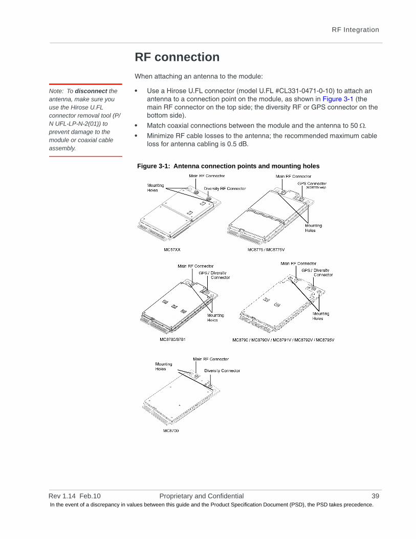
RF connection
When attaching an antenna to the module:
Note: To disconnect the antenna, make sure you use the Hirose U.FL connector removal tool (P/N UFL-LP-N-2(01)) to prevent damage to the module or coaxial cable assembly.
• Use a Hirose U.FL connector (model U.FL #CL331-0471-0-10) to attach an antenna to a connection point on the module, as shown in Figure 3-1 (the main RF connector on the top side; the diversity RF or GPS connector on the bottom side).
• Match coaxial connections between the module and the antenna to 50 • Minimize RF cable losses to the antenna; the recommended maximum cable
loss for antenna cabling is 0.5 dB.
Figure 3-1: Antenna connection points and mounting holes
Rev 1.14 Feb.10 Proprietary and Confidential 39 In the event of a discrepancy in values between this guide and the Product Specification Document (PSD), the PSD takes precedence.
CDMA and GSM / UMTS Mini Card Hardware Integration Guide
Ground connectionWhen connecting the module to system ground:
• Prevent noise leakage by establishing a very good ground connection to the module through the host connector.
• Connect to system ground using the two mounting holes at the top of the module (as shown in Figure 3-1).
• Minimize ground noise leakage into the RF.Depending on the host board design, noise could potentially be coupled to the module from the host board. This is mainly an issue for host designs that have signals traveling along the length of the module, or circuitry operating at both ends of the module interconnects.
ShieldingThe module is fully shielded to protect against EMI and to ensure compliance with FCC Part 15 - “Radio Frequency Devices” (or equivalent regulations in other jurisdictions).
Note: The module shields must NOT be removed.
Note: Values in this guide are taken from the appro-priate product specifi-cation documents (PSDs) (listed in Related documents, page 13) — in the case of a discrepancy between this document and the relevant PSD, use the value listed in the PSD.
Antenna and cabling
When selecting the antenna and cable, it is critical to RF performance to match antenna gain and cable loss.
Choosing the correct antenna and cabling
Consider the following points for proper matching of antennas and cabling:
• The antenna (and associated circuitry) should have a nominal impedance of 50 with a return loss 10 dB across each frequency band of operation.
• The system gain value affects both radiated power and regulatory (FCC, IC, CE, etc.) test results.
Developing custom antennas
Consider the following points when developing custom-designed antennas:
• A skilled RF engineer should do the development to ensure that the RF performance is maintained.
• Identify the bands that need to be supported, particularly when both the MC57xx and MC87xx will be installed in the same platform. In this case, you may want to develop separate antennas for maximum performance.
Note: For detailed electrical performance criteria, see Appendix A: Antenna Specification, page 97.
40 Proprietary and Confidential 2130114 In the event of a discrepancy in values between this guide and the Product Specification Document (PSD), the PSD takes precedence.
RF Integration
Determining the antenna’s location
Consider the following points when deciding where to put the antenna:
• Antenna location may affect RF performance. Although the module is shielded to prevent interference in most applications, the placement of the antenna is still very important — if the host device is insufficiently shielded, high levels of broadband or spurious noise can degrade the module’s perfor-mance.
• Connecting cables between the module and the antenna must have 50 impedance. If the impedance of the module is mismatched, RF performance is reduced significantly.
• Antenna cables should be routed, if possible, away from noise sources (switching power supplies, LCD assemblies, etc.). If the cables are near the noise sources, the noise may be coupled into the RF cable and into the antenna.
Disabling the diversity antenna
• MC57xx—If your host device is not designed to use the MC57xx module’s diversity antenna, terminate the interface with a 50 load.
• MC8780/MC8781/MC8790/MC8790V/MC8791V/MC8792V/MC8795V/MC8700—Use the AT command !RXDEN=0 to disable receive diversity or !RXDEN=1 to enable receive diversity.
Note: These modules are based on ZIF (Zero Inter-mediate Frequency) technologies; when performing EMC (Electro-magnetic Compatibility) tests, there are no IF (Intermediate Frequency) components from the module to consider.
Interference and sensitivitySeveral sources of interference can affect the RF performance of the module (RF desense). Common sources include power supply noise and device-generated RF.
RF desense can be addressed through a combination of mitigation techniques and radiated sensitivity measurement.
Power supply noise
Noise in the power supply can lead to noise in the RF signal.
Note: Values in this guide are taken from the appro-priate product specifi-cation documents (PSDs) (listed in Related documents, page 13) — in the case of a discrepancy between this document and the relevant PSD, use the value listed in the PSD.
The power supply ripple limit for the module is no more than 200 mVp-p 1 Hz to 100 kHz. This limit includes voltage ripple due to transmitter burst activity.
Interference from other wireless devices
Wireless devices operating inside the host device can cause interference that affects the module.
To determine the most suitable locations for antennas on your host device, evaluate each wireless device’s radio system, considering the following:
• Any harmonics, sub-harmonics, or cross-products of signals generated by wireless devices that fall in the module’s Rx range may cause spurious response, resulting in decreased Rx performance.
Rev 1.14 Feb.10 Proprietary and Confidential 41 In the event of a discrepancy in values between this guide and the Product Specification Document (PSD), the PSD takes precedence.
CDMA and GSM / UMTS Mini Card Hardware Integration Guide
• The Tx power and corresponding broadband noise of other wireless devices may overload or increase the noise floor of the module’s receiver, resulting in Rx desense.
The severity of this interference depends on the closeness of the other antennas to the module’s antenna. To determine suitable locations for each wireless device’s antenna, thoroughly evaluate your host device’s design.
Device-generated RF
Note: The module can cause interference with other devices such as hearing aids and on-board speakers.
Wireless devices such as the Mini Card transmit in bursts (pulse transients) for set durations (RF burst frequencies). Hearing aids and speakers convert these burst frequencies into audible frequencies, resulting in audible noise.
All electronic computing devices generate RF interference that can negatively affect the receive sensitivity of the module.
The proximity of host electronics to the antenna in wireless devices can contribute to decreased Rx performance. Components that are most likely to cause this include:
• Microprocessor and memory
• Display panel and display drivers
• Switching-mode power supplies
These and other high-speed devices (in particular, the processor) can decrease Rx performance because they run at frequencies of tens of MHz. The rapid rise and fall of these clock signals generates higher-order harmonics that often fall within the operating frequency band of the module, affecting the module’s receive sensitivity.
Example
On a sub-system running at 40 MHz, the 22nd harmonic falls at 880 MHz, which is within the cellular receive frequency band.
Note: In practice, there are usually numerous interfering frequencies and harmonics. The net effect can be a series of desensitized receive channels.
Note: It is important to investigate sources of localized interference early in the design cycle.
Methods to mitigate decreased Rx performance
To reduce the effect of device-generated RF on Rx performance:
• Put the antenna as far as possible from sources of interference. The drawback is that the module may be less convenient to use.
• Shield the host device. The module itself is well shielded to avoid external interference. However, the antenna cannot be shielded for obvious reasons. In most instances, it is necessary to employ shielding on the components of the host device (such as the main processor and parallel bus) that have the highest RF emissions.
• Filter out unwanted high-order harmonic energy by using discrete filtering on low frequency lines.
• Form shielding layers around high-speed clock traces by using multi-layer PCBs.
• Route antenna cables away from noise sources.
42 Proprietary and Confidential 2130114 In the event of a discrepancy in values between this guide and the Product Specification Document (PSD), the PSD takes precedence.
RF Integration
Radiated sensitivity measurement
A wireless device contains many sources of noise that contribute to a reduction in Rx performance.
To determine the extent of any desensitization of receiver performance due to self-generated noise in the host device, over-the-air (OTA) or radiated testing is required. This testing can be performed by Sierra Wireless or you can use your own OTA test chamber for in-house testing.
Sierra Wireless’ sensitivity testing and desensitization investigation
Most carriers require a certain level of receiver performance to ensure proper functioning of the device on their networks. Although the module has been designed to meet these carrier requirements, it is still susceptible to various performance inhibitors.
As part of the Engineering Services package, Sierra Wireless offers modem OTA sensitivity testing and desensitization (desense) investigation. For more information, contact your account manager or the Sales Desk (see page 5).
Note: Sierra Wireless has the capability to measure TIS (Total Isotropic Sensitivity) and TRP (Total Radiated Power) according to CTIA's published test procedure.
OTA test chamber configuration
To make OTA measurements, a test chamber is required. A full-size anechoic chamber is not necessarily required. Figure 3-2 shows a small anechoic chamber manufactured by Lindgren. This does not provide power to the same accuracy as a full-size anechoic chamber, but is sufficient for this application. A base station simulator, such as an Agilent 8960 (shown) or Rohde & Schwarz CMU200, is used to provide FER (Frame Error Rate) measurements.
Rev 1.14 Feb.10 Proprietary and Confidential 43 In the event of a discrepancy in values between this guide and the Product Specification Document (PSD), the PSD takes precedence.
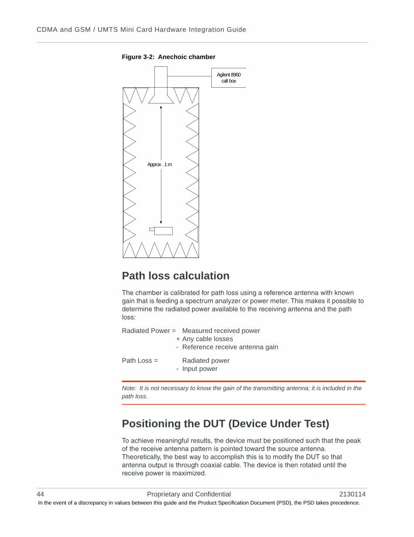
CDMA and GSM / UMTS Mini Card Hardware Integration Guide
Figure 3-2: Anechoic chamber
Path loss calculation
The chamber is calibrated for path loss using a reference antenna with known gain that is feeding a spectrum analyzer or power meter. This makes it possible to determine the radiated power available to the receiving antenna and the path loss:
Radiated Power = Measured received power+ Any cable losses- Reference receive antenna gain
Path Loss = Radiated power- Input power
Note: It is not necessary to know the gain of the transmitting antenna; it is included in the path loss.
Positioning the DUT (Device Under Test)
To achieve meaningful results, the device must be positioned such that the peak of the receive antenna pattern is pointed toward the source antenna. Theoretically, the best way to accomplish this is to modify the DUT so that antenna output is through coaxial cable. The device is then rotated until the receive power is maximized.
Approx . 1 m
Agilent 8960call box
44 Proprietary and Confidential 2130114 In the event of a discrepancy in values between this guide and the Product Specification Document (PSD), the PSD takes precedence.
RF Integration
Alternate path loss calculation method
Path loss can also be calculated, without modifying the DUT, by using the transmit capabilities of the unit. This method of calculation is possible because the position that maximizes transmitter power provides a sufficiently accurate location for receiver desense measurements. The unit is placed in a call and set to generate peak output power, either through a test mode, or by configuring the base station simulator to issue the appropriate command. The unit is then positioned for maximum power as determined by the call box.
Sensitivity vs. frequency
For the MC57xx, sensitivity is defined as the input power level in dBm that produces a FER (Frame Error Rate) of 0.5%. Sensitivity should be measured at all CDMA frequencies across each band. For example, Figure 3-3 illustrates sensitivity in the US PCS band. There are 25 physical channels with a spacing of 50 KHz; the first CDMA channel is CH25.
For the MC87xx, sensitivity is defined as the input power level in dBm that produces a BER (Bit Error Rate) of 2% (GSM) or 0.1% (UMTS). Sensitivity should be measured at all GSM / UMTS frequencies across each band, as shown in Figures 3-4 through 3-11.
Rev 1.14 Feb.10 Proprietary and Confidential 45 In the event of a discrepancy in values between this guide and the Product Specification Document (PSD), the PSD takes precedence.
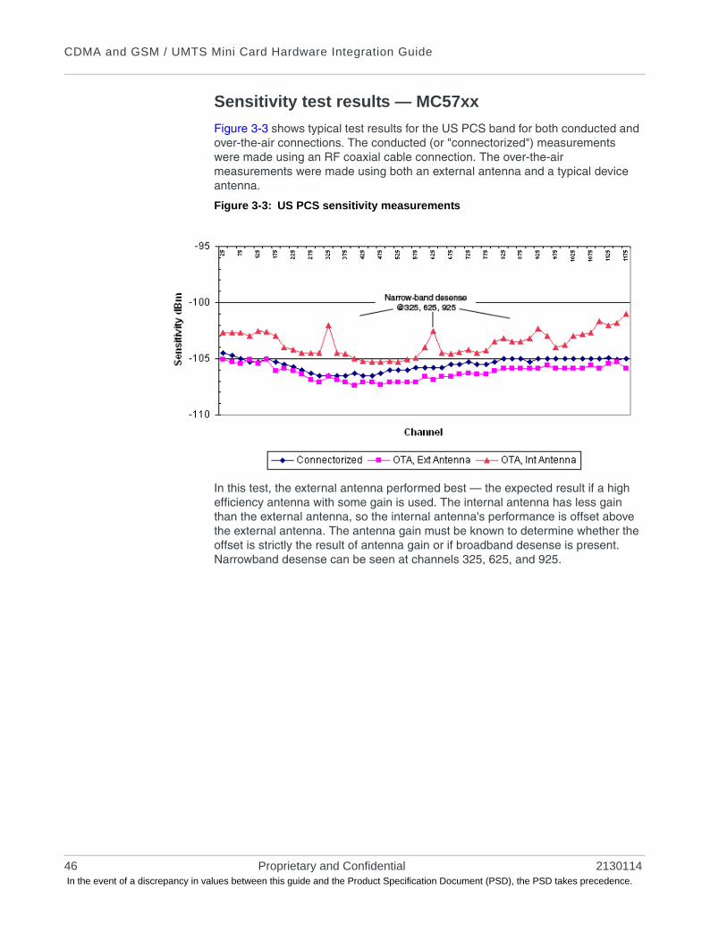
CDMA and GSM / UMTS Mini Card Hardware Integration Guide
Sensitivity test results — MC57xx
Figure 3-3 shows typical test results for the US PCS band for both conducted and over-the-air connections. The conducted (or "connectorized") measurements were made using an RF coaxial cable connection. The over-the-air measurements were made using both an external antenna and a typical device antenna.
Figure 3-3: US PCS sensitivity measurements
In this test, the external antenna performed best — the expected result if a high efficiency antenna with some gain is used. The internal antenna has less gain than the external antenna, so the internal antenna's performance is offset above the external antenna. The antenna gain must be known to determine whether the offset is strictly the result of antenna gain or if broadband desense is present. Narrowband desense can be seen at channels 325, 625, and 925.
46 Proprietary and Confidential 2130114 In the event of a discrepancy in values between this guide and the Product Specification Document (PSD), the PSD takes precedence.
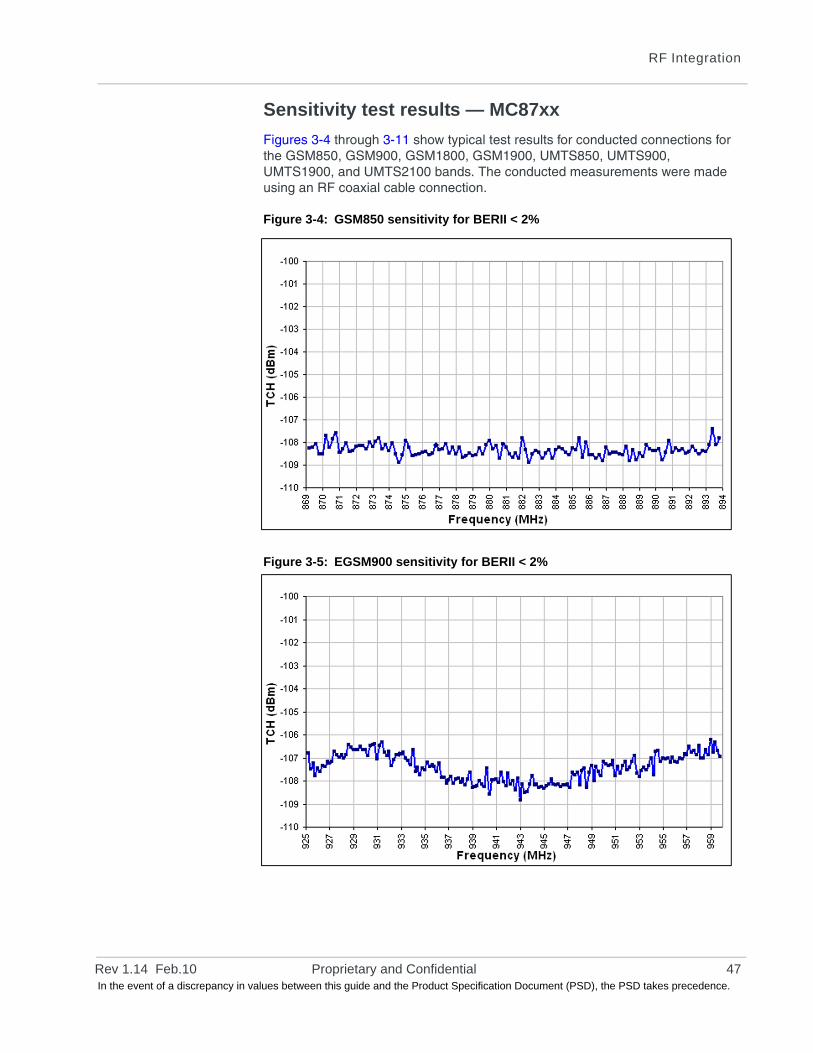
RF Integration
Sensitivity test results — MC87xx
Figures 3-4 through 3-11 show typical test results for conducted connections for the GSM850, GSM900, GSM1800, GSM1900, UMTS850, UMTS900, UMTS1900, and UMTS2100 bands. The conducted measurements were made using an RF coaxial cable connection.
Figure 3-4: GSM850 sensitivity for BERII < 2%
Figure 3-5: EGSM900 sensitivity for BERII < 2%
Rev 1.14 Feb.10 Proprietary and Confidential 47 In the event of a discrepancy in values between this guide and the Product Specification Document (PSD), the PSD takes precedence.
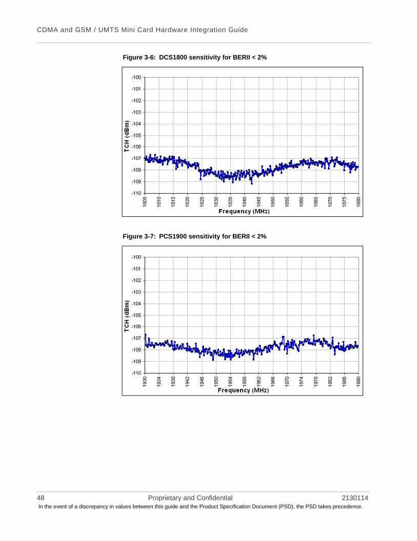
CDMA and GSM / UMTS Mini Card Hardware Integration Guide
Figure 3-6: DCS1800 sensitivity for BERII < 2%
Figure 3-7: PCS1900 sensitivity for BERII < 2%
48 Proprietary and Confidential 2130114 In the event of a discrepancy in values between this guide and the Product Specification Document (PSD), the PSD takes precedence.
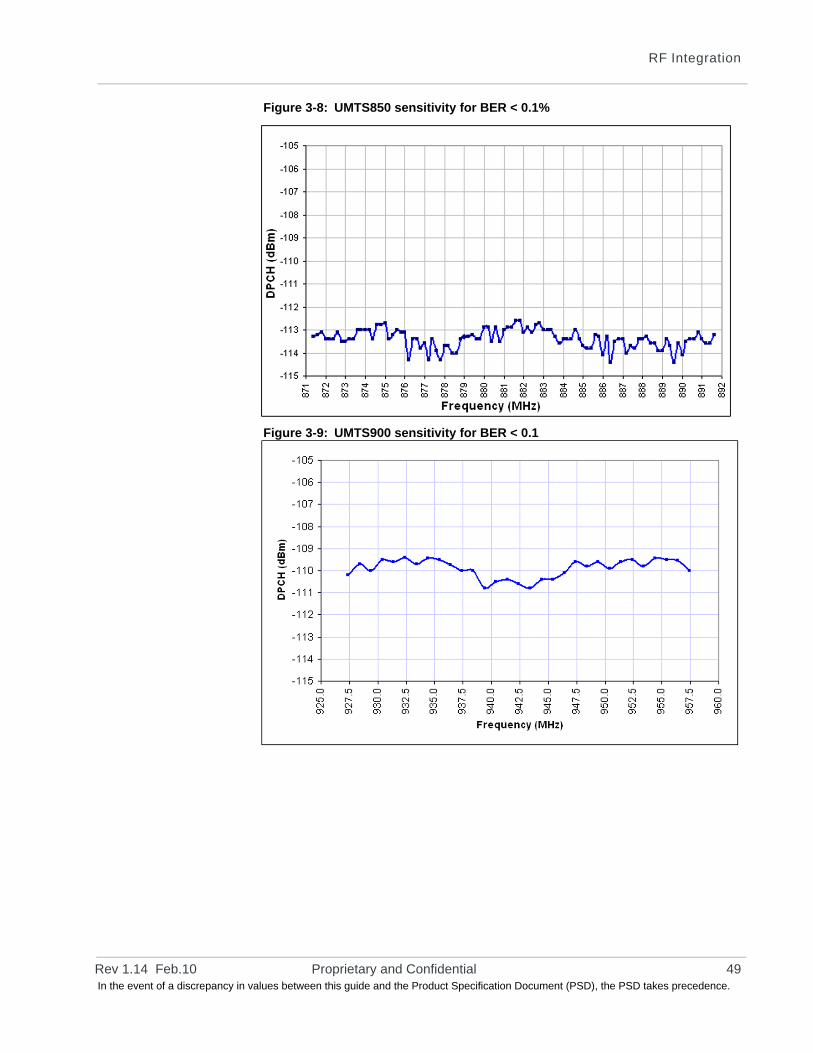
RF Integration
Figure 3-8: UMTS850 sensitivity for BER < 0.1%
Figure 3-9: UMTS900 sensitivity for BER < 0.1
Rev 1.14 Feb.10 Proprietary and Confidential 49 In the event of a discrepancy in values between this guide and the Product Specification Document (PSD), the PSD takes precedence.
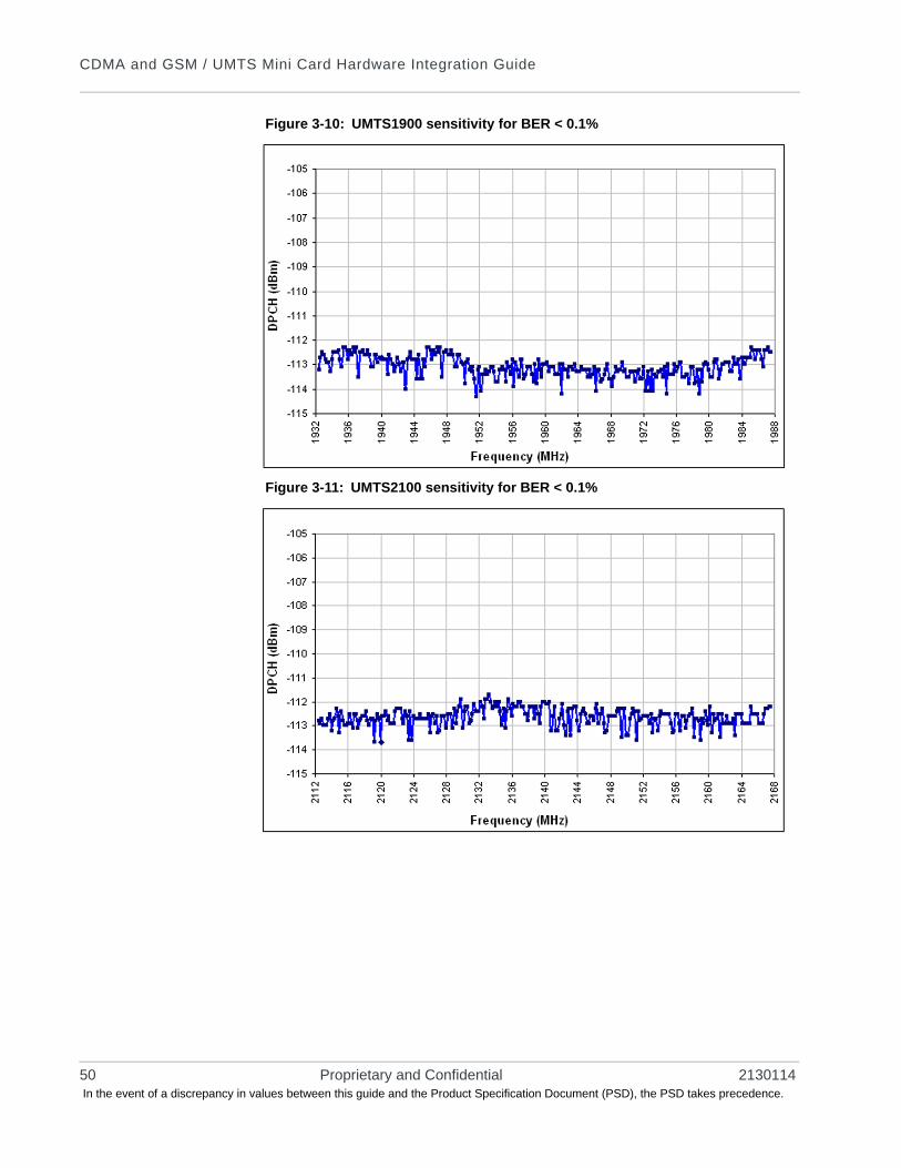
CDMA and GSM / UMTS Mini Card Hardware Integration Guide
Figure 3-10: UMTS1900 sensitivity for BER < 0.1%
Figure 3-11: UMTS2100 sensitivity for BER < 0.1%
50 Proprietary and Confidential 2130114 In the event of a discrepancy in values between this guide and the Product Specification Document (PSD), the PSD takes precedence.
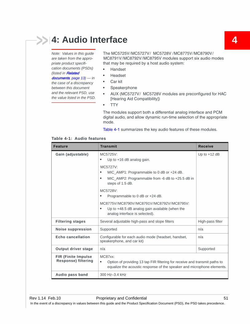
Rev 1.14 In the event
44: Audio InterfaceNote: Values in this guide are taken from the appro-priate product specifi-cation documents (PSDs) (listed in Related documents, page 13) — in the case of a discrepancy between this document and the relevant PSD, use the value listed in the PSD.
The MC5725V/MC5727V/ MC5728V /MC8775V/MC8790V/MC8791V/MC8792V/MC8795V modules support six audio modes that may be required by a host audio system:
• Handset
• Headset
• Car kit
• Speakerphone
• AUX (MC5727V/ MC5728V modules are preconfigured for HAC [Hearing Aid Compatibility])
• TTY
The modules support both a differential analog interface and PCM digital audio, and allow dynamic run-time selection of the appropriate mode.
Table 4-1 summarizes the key audio features of these modules.
Table 4-1: Audio features
Feature Transmit Receive
Gain (adjustable) MC5725V:
• Up to +16 dB analog gain.
MC5727V:
• MIC_AMP1: Programmable to 0 dB or +24 dB.
• MIC_AMP2: Programmable from -6 dB to +25.5 dB in steps of 1.5 dB.
MC5728V:
• Programmable to 0 dB or +24 dB.
MC8775V/MC8790V/MC8791V/MC8792V/MC8795V:
• Up to +48.5 dB analog gain available (when the analog interface is selected).
Up to +12 dB
Filtering stages Several adjustable high-pass and slope filters High-pass filter
Noise suppression Supported n/a
Echo cancellation Configurable for each audio mode (headset, handset, speakerphone, and car kit)
n/a
Output driver stage n/a Supported
FIR (Finite Impulse Response) filtering
MC87xx:
• Option of providing 13 tap FIR filtering for receive and transmit paths to equalize the acoustic response of the speaker and microphone elements.
Audio pass band 300 Hz–3.4 kHz
Feb.10 Proprietary and Confidential 51of a discrepancy in values between this guide and the Product Specification Document (PSD), the PSD takes precedence.
CDMA and GSM / UMTS Mini Card Hardware Integration Guide
These modules are intended to serve as an integral component of a more complex audio system—for example, a PDA with a separate codec interfaced to the Host Application processor.
Usually, the interface between the module and the host audio system is set to line-level amplitudes with no transducer considerations. The responsibility of the module codec or host codec for special functions is detailed in Table 4-2.
System block diagrams
Note: When integrating the module into your host platform, make sure the module has sufficient shielding to prevent RF interference.
MC5725V / MC5727V system block
Figure 4-1 represents the MC5725V / MC5727V module’s audio system block, and includes the following features:
• Module interconnects are shown on the left side of the diagram. The audio interface uses the signals:· MIC_P / MIC_N· SPK_P / SPK_N
Note: Make sure the host device includes DC blocking capacitors on the Audio In lines – the module does not include series capacitors.
• Dynamic ranges for each programmable gain stage are listed, with the following constraints:· MIC_AMP1 is programmable in discrete steps only· MIC_AMP2 (MC5727V only) is programmable in discrete steps only· CodecSTGain, when set to the minimum setting, effectively mutes sidetone
in the module codec
Table 4-2: Functions - responsibility codecs
Function Responsible Codec
Phone oriented (e.g., echo cancellation, FIR filtering)
Module codec
Path-switching Host codec
Transducer interfaces Host codec
Adjustable gain / volume settings Either
DTMF / ringer tone generation Either
Mixing Host codec
52 Proprietary and Confidential 2130114 In the event of a discrepancy in values between this guide and the Product Specification Document (PSD), the PSD takes precedence.
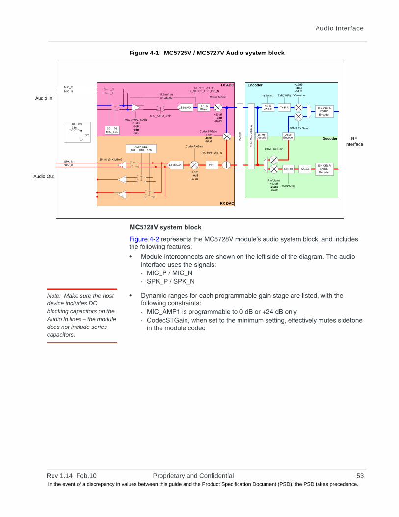
Audio Interface
Aud
Aud
Figure 4-1: MC5725V / MC5727V Audio system block
MC5728V system block
Figure 4-2 represents the MC5728V module’s audio system block, and includes the following features:
• Module interconnects are shown on the left side of the diagram. The audio interface uses the signals:· MIC_P / MIC_N· SPK_P / SPK_N
Note: Make sure the host device includes DC blocking capacitors on the Audio In lines – the module does not include series capacitors.
• Dynamic ranges for each programmable gain stage are listed, with the following constraints:· MIC_AMP1 is programmable to 0 dB or +24 dB only· CodecSTGain, when set to the minimum setting, effectively mutes sidetone
in the module codec
Decoder
RX DAC
EncoderTX ADC
HPF & Slope
HPF
Ech
o C
an
cella
tion
NS & AAGC
Tx FIR
Rx FIR13K CELP/
EVRC Decoder
AAGC
13 bit A/D
13 bit D/A
CodecRxGain
RX_HPF_DIS_N
CodecSTGain
CodecTxGain
TX_HPF_DIS_NTX_SLOPE_FILT_DIS_N
MIC_AMP1_GAIN+16dB+8dB+6dB-2dB
nsSwitch TxPCMFilt TxVolume
RxVolume
RxPCMFilt
AMP_SEL001 010 100
10 01MIC_SEL
35mW @ +3dBm0
RF Filter33n
22p
MIC_AMP2_BYP
PC
M I/
F
+12dB-25dB-84dB
+12dB-3dB-84dB
+12dB0dB
-81dB
+12dB-48dB-96dB
+12dB0dB
-84dB
57.3mVrms@ 0dBm0
SPK_P
SPK_N
MIC_P
MIC_N
13K CELP/EVRC
Encoder
DTMFEncoder
DTMF Rx Gain
DTMF Tx Gain
DTMFDecoder
io In
io Out
RF Interface
Rev 1.14 Feb.10 Proprietary and Confidential 53 In the event of a discrepancy in values between this guide and the Product Specification Document (PSD), the PSD takes precedence.
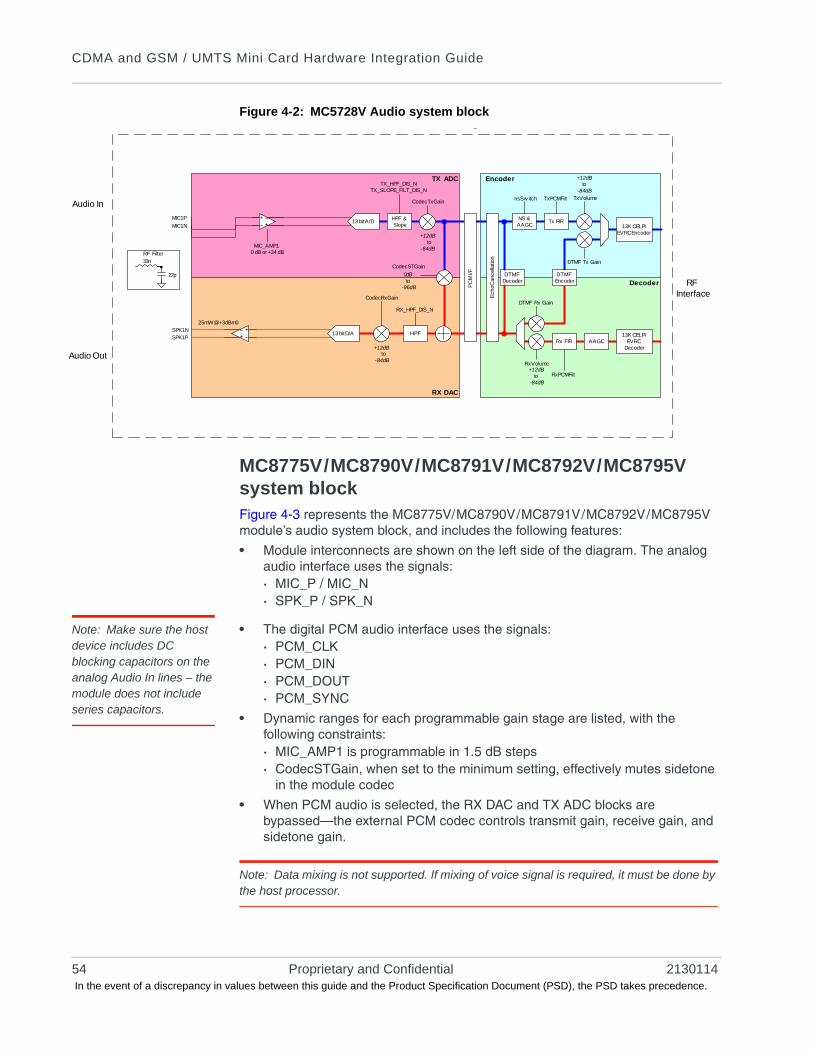
CDMA and GSM / UMTS Mini Card Hardware Integration Guide
Figure 4-2: MC5728V Audio system block
MC8775V/MC8790V/MC8791V/MC8792V/MC8795V system blockFigure 4-3 represents the MC8775V/MC8790V/MC8791V/MC8792V/MC8795V module’s audio system block, and includes the following features:
• Module interconnects are shown on the left side of the diagram. The analog audio interface uses the signals:· MIC_P / MIC_N· SPK_P / SPK_N
Note: Make sure the host device includes DC blocking capacitors on the analog Audio In lines – the module does not include series capacitors.
• The digital PCM audio interface uses the signals:· PCM_CLK· PCM_DIN· PCM_DOUT· PCM_SYNC
• Dynamic ranges for each programmable gain stage are listed, with the following constraints:· MIC_AMP1 is programmable in 1.5 dB steps· CodecSTGain, when set to the minimum setting, effectively mutes sidetone
in the module codec
• When PCM audio is selected, the RX DAC and TX ADC blocks are bypassed—the external PCM codec controls transmit gain, receive gain, and sidetone gain.
Note: Data mixing is not supported. If mixing of voice signal is required, it must be done by the host processor.
Decoder
RX DAC
EncoderTX ADC
HPF &Slope
HPF
Ech
o Can
cella
tion
NS &AAGC
Tx FIR
Rx FIR13K CELP/
EVRCDecoder
AAGC
13 bit A/D
13 bit D/A
CodecRxGain
RX_HPF_DIS_N
CodecSTGain
CodecTxGain
TX_HPF_DIS_NTX_SLOPE_FILT_DIS_N
MIC_AMP10 dB or +24 dB
nsSw itch TxPCMFilt TxVolume
RxVolume
RxPCMFilt
25mW @ +3dBm0
RF Filter33n
22p
PC
M I/
F
+12dBto
-84dB
+12dBto
-84dB
+12dB to
-84dB
0dBto
-96dB
+12dB to
-84dB
g
SPK1NSPK1P
MIC1P
MIC1N 13K CELP/EVRC Encoder
DTMFEncoder
DTMF Rx Gain
DTMF Tx Gain
DTMFDecoder
Audio In
Audio Out
RFInterface
54 Proprietary and Confidential 2130114 In the event of a discrepancy in values between this guide and the Product Specification Document (PSD), the PSD takes precedence.
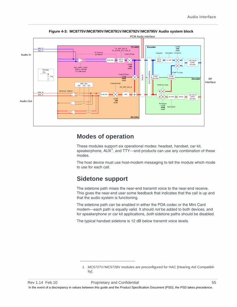
Audio Interface
Aud
Aud
Figure 4-3: MC8775V/MC8790V/MC8791V/MC8792V/MC8795V Audio system block
Modes of operation
These modules support six operational modes: headset, handset, car kit, speakerphone, AUX1, and TTY—end products can use any combination of these modes.
The host device must use host-modem messaging to tell the module which mode to use for each call.
Sidetone support
The sidetone path mixes the near-end transmit voice to the near-end receive. This gives the near-end user some feedback that indicates that the call is up and that the audio system is functioning.
The sidetone path can be enabled in either the PDA codec or the Mini Card modem—each path is equally valid. It should not be added to both devices, and for speakerphone or car kit applications, both sidetone paths should be disabled.
The typical handset sidetone is 12 dB below transmit voice levels.
Decoder
RX DAC
EncoderTX ADC
HPF & Slope
HPF
Ech
o C
an
cella
tion
NS & AAGC
Tx FIR
Rx FIR13K CELP/
EVRC Decoder
AAGC
13 bit A/D
13 bit D/A
CodecRxGain
RX_HPF_DIS_N
CodecSTGain
CodecTxGain
TX_HPF_DIS_NTX_SLOPE_FILT_DIS_N
MIC_AMP1_GAIN-6dB to +49.5dBin 1.5dB steps
nsSwitch TxPCMFilt TxVolume
RxVolume
RxPCMFilt
AMP_SEL001 010 100
35mW @ +3dBm0
RF Filter33n
22p
PC
M I/
F
+12dB-25dB-84dB
+12dB-3dB-84dB
+12dB0dB
-81dB
+12dB-48dB-96dB
+12dB0dB
-84dB
57.3mVrms@ 0dBm0
SPK_P
SPK_N
MIC_P
MIC_N
13K CELP/EVRC
Encoder
DTMFEncoder
DTMF Rx Gain
DTMF Tx Gain
DTMFDecoder
io In
io Out
RF Interface
PCM Audio interface
1. MC5727V/MC5728V modules are preconfigured for HAC [Hearing Aid Compatibil-ity].
Rev 1.14 Feb.10 Proprietary and Confidential 55 In the event of a discrepancy in values between this guide and the Product Specification Document (PSD), the PSD takes precedence.
CDMA and GSM / UMTS Mini Card Hardware Integration Guide
Gain distribution
For Handset and Headset mode, the threshold of pain (+120 dBSPL) must not be exceeded at the maximum volume setting. A good target for the medium volume setting is +94 dBSPL, as this is a typical level for conversational speech.
Most audio gain should be added to the host audio front end (within the PDA style codec gain blocks or amplifiers between the host codec and transducers). Refer to the appropriate Mini Card Product Specification Document for reference levels on the modem receive and transmit side.
Echo cancellation support
The Mini Card offers four modes of echo cancellation to support unique end-unit audio capabilities (echo cancellation can also be turned off completely). All echo cancellation is near-end (mobile TX) cancellation only. The network provides some level of far-end echo cancellation.
Table 4-3: System gain values1
Mode Modem TX gain (dB)
Modem RX gain (dB)
Typical system TX gain (dB)
Typical system RX gain (dB)
Handset +8 +8 +28 +32
Headset +8 +8 +28 +24
Car Kit +16 +8 +36 +32
Speakerphone +16 +8 +36 +32
1 Typical system gains are estimates only and vary from system to system depend-ing upon transducer sensitivity.
Table 4-4: Echo cancellation details
Mode Details
Handset • Short echo path (<16 ms travel time from speaker to microphone)
• Handset design requires good isolation between speaker and microphone
• Echo canceller allows full-duplex conversation with absolute minimum echo
Headset • Short echo path (<16 ms travel time from speaker to microphone)
• Headset design may allow higher echo than handset mode—microphone and speaker are physically closer
• More aggressive echo canceller algorithm allows full-duplex conversation on headsets with good isolation
56 Proprietary and Confidential 2130114 In the event of a discrepancy in values between this guide and the Product Specification Document (PSD), the PSD takes precedence.
Audio Interface
Audio signal interface
The differential microphone input offers superior noise rejection performance to the single-ended approach. The termination of the differential pair rejects common signals (such as noise). The pair should be routed together for optimal noise rejection. Since MIC_P and MIC_N are high impedance inputs, it is important to isolate these from possible noise sources (toggling digital lines with fast edges).
The speaker interface can be single-ended or differential depending on product. Single-ended speaker outputs rely on modem ground as an audio reference.
The audio passband for both receive and transmit paths (speaker and microphone) extends from 300 Hz to 3.4 kHz. A programmable sidetone with a range from mute to unity gain is available for both headset and main audio paths. Sidetone should be muted for speakerphone use.
Note that certain carriers now require use of hearing-aid compatible transducers in a handset design. The Primary audio path can be interfaced directly to such devices. Refer to ANSI C63.19 for details regarding reduced RF emissions ("U3 rating") and inductive / telecoil coupling ("U3T" rating) devices.
Car kit • Long echo path (<64 ms travel time from speaker to micro-phone)
• Loud echo
• For use with hands-free car kit or speakerphone applica-tions with mild distortion
Speakerphone • Long echo path (<64 ms travel time from speaker to micro-phone)
• Loud echo
• For use with speakerphone applications with high distortion
• Half-duplex algorithm, very aggressive in near-end Tx muting to eliminate transmitted echo
Off
Table 4-5: Primary audio signal interface
Signal Pin # Type Direction Description
MIC_P 1 Analog Input Non-inverted microphone input (+)
MIC_N 3 Analog Input Inverted microphone input (-)
SPK_P 5 Analog Output Non-inverted speaker output (+)
SPK_N 7 Analog Output Inverted speaker output (-)
Table 4-4: Echo cancellation details (Continued)
Mode Details
Rev 1.14 Feb.10 Proprietary and Confidential 57 In the event of a discrepancy in values between this guide and the Product Specification Document (PSD), the PSD takes precedence.
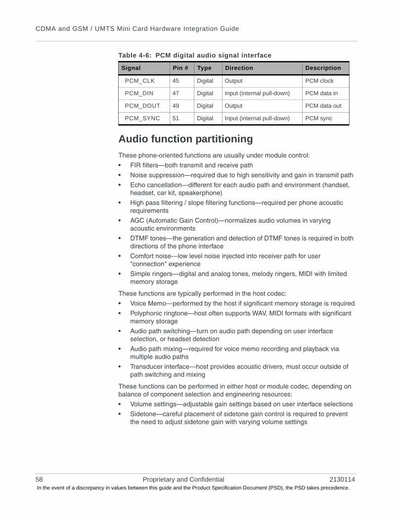
CDMA and GSM / UMTS Mini Card Hardware Integration Guide
Audio function partitioning
These phone-oriented functions are usually under module control:
• FIR filters—both transmit and receive path
• Noise suppression—required due to high sensitivity and gain in transmit path
• Echo cancellation—different for each audio path and environment (handset, headset, car kit, speakerphone)
• High pass filtering / slope filtering functions—required per phone acoustic requirements
• AGC (Automatic Gain Control)—normalizes audio volumes in varying acoustic environments
• DTMF tones—the generation and detection of DTMF tones is required in both directions of the phone interface
• Comfort noise—low level noise injected into receiver path for user "connection" experience
• Simple ringers—digital and analog tones, melody ringers, MIDI with limited memory storage
These functions are typically performed in the host codec:
• Voice Memo—performed by the host if significant memory storage is required
• Polyphonic ringtone—host often supports WAV, MIDI formats with significant memory storage
• Audio path switching—turn on audio path depending on user interface selection, or headset detection
• Audio path mixing—required for voice memo recording and playback via multiple audio paths
• Transducer interface—host provides acoustic drivers, must occur outside of path switching and mixing
These functions can be performed in either host or module codec, depending on balance of component selection and engineering resources:
• Volume settings—adjustable gain settings based on user interface selections
• Sidetone—careful placement of sidetone gain control is required to prevent the need to adjust sidetone gain with varying volume settings
Table 4-6: PCM digital audio signal interface
Signal Pin # Type Direction Description
PCM_CLK 45 Digital Output PCM clock
PCM_DIN 47 Digital Input (internal pull-down) PCM data in
PCM_DOUT 49 Digital Output PCM data out
PCM_SYNC 51 Digital Input (internal pull-down) PCM sync
58 Proprietary and Confidential 2130114 In the event of a discrepancy in values between this guide and the Product Specification Document (PSD), the PSD takes precedence.
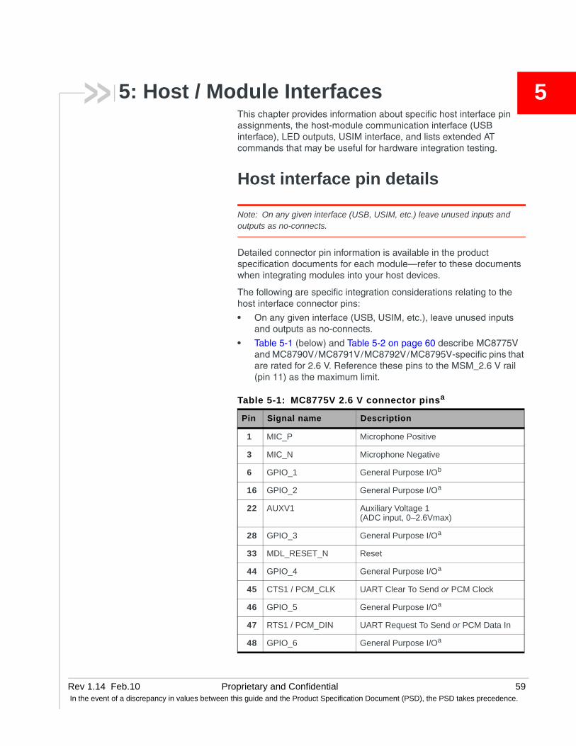
Rev 1.14 In the event
55: Host / Module InterfacesThis chapter provides information about specific host interface pin assignments, the host-module communication interface (USB interface), LED outputs, USIM interface, and lists extended AT commands that may be useful for hardware integration testing.
Host interface pin details
Note: On any given interface (USB, USIM, etc.) leave unused inputs and outputs as no-connects.
Detailed connector pin information is available in the product specification documents for each module—refer to these documents when integrating modules into your host devices.
The following are specific integration considerations relating to the host interface connector pins:
• On any given interface (USB, USIM, etc.), leave unused inputs and outputs as no-connects.
• Table 5-1 (below) and Table 5-2 on page 60 describe MC8775V and MC8790V/MC8791V/MC8792V/MC8795V-specific pins that are rated for 2.6 V. Reference these pins to the MSM_2.6 V rail (pin 11) as the maximum limit.
Table 5-1: MC8775V 2.6 V connector pinsa
Pin Signal name Description
1 MIC_P Microphone Positive
3 MIC_N Microphone Negative
6 GPIO_1 General Purpose I/Ob
16 GPIO_2 General Purpose I/Oa
22 AUXV1 Auxiliary Voltage 1(ADC input, 0–2.6Vmax)
28 GPIO_3 General Purpose I/Oa
33 MDL_RESET_N Reset
44 GPIO_4 General Purpose I/Oa
45 CTS1 / PCM_CLK UART Clear To Send or PCM Clock
46 GPIO_5 General Purpose I/Oa
47 RTS1 / PCM_DIN UART Request To Send or PCM Data In
48 GPIO_6 General Purpose I/Oa
Feb.10 Proprietary and Confidential 59of a discrepancy in values between this guide and the Product Specification Document (PSD), the PSD takes precedence.
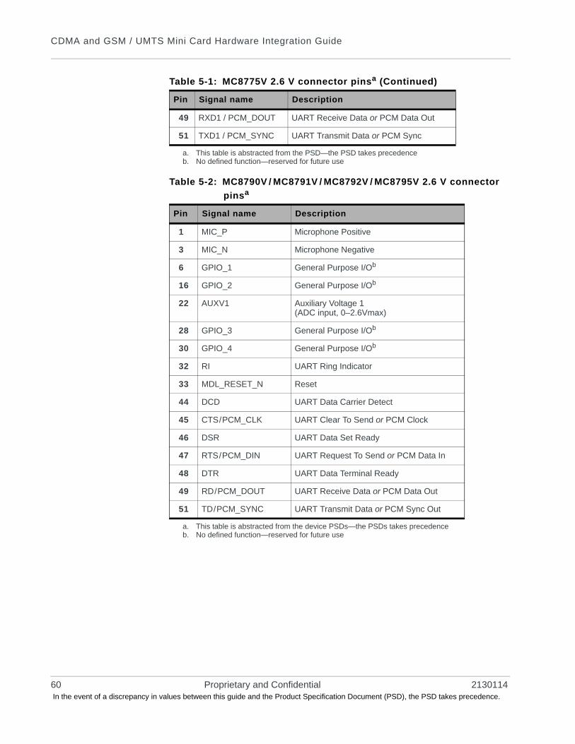
CDMA and GSM / UMTS Mini Card Hardware Integration Guide
49 RXD1 / PCM_DOUT UART Receive Data or PCM Data Out
51 TXD1 / PCM_SYNC UART Transmit Data or PCM Sync
a. This table is abstracted from the PSD—the PSD takes precedenceb. No defined function—reserved for future use
Table 5-2: MC8790V / MC8791V / MC8792V / MC8795V 2.6 V connector
pinsa
Pin Signal name Description
1 MIC_P Microphone Positive
3 MIC_N Microphone Negative
6 GPIO_1 General Purpose I/Ob
16 GPIO_2 General Purpose I/Ob
22 AUXV1 Auxiliary Voltage 1(ADC input, 0–2.6Vmax)
28 GPIO_3 General Purpose I/Ob
30 GPIO_4 General Purpose I/Ob
32 RI UART Ring Indicator
33 MDL_RESET_N Reset
44 DCD UART Data Carrier Detect
45 CTS/PCM_CLK UART Clear To Send or PCM Clock
46 DSR UART Data Set Ready
47 RTS/PCM_DIN UART Request To Send or PCM Data In
48 DTR UART Data Terminal Ready
49 RD/PCM_DOUT UART Receive Data or PCM Data Out
51 TD/PCM_SYNC UART Transmit Data or PCM Sync Out
a. This table is abstracted from the device PSDs—the PSDs takes precedenceb. No defined function—reserved for future use
Table 5-1: MC8775V 2.6 V connector pinsa (Continued)
Pin Signal name Description
60 Proprietary and Confidential 2130114 In the event of a discrepancy in values between this guide and the Product Specification Document (PSD), the PSD takes precedence.
Host / Module Interfaces
USB interface
The USB interface is the only path for communication between the host and module.
The interface complies with the Universal Serial Bus Specification, Rev 2.0.
Features of the USB interface include:
• Support for the full-speed (12 Mbps) data rate
• (MC8790/MC8790V/MC8791V/MC8792V/MC8795V/MC8700) Support for the high-speed (480 Mbps) data rate
• Transfer of general, phone diagnostic, and over-the-air data between the module and the host
• Enumeration of the module as a set of Modem (MC57xx) or COM (MC57xx and MC87xx) ports, using host Windows drivers
• Enumeration of the module as a set of /dev/ttyUSBn devices for Linux systems with the Sierra Wireless driver installed
• USB-compliant transceivers
USB handshaking
Note: If you are using the Windows or Linux drivers provided by Sierra Wireless, you can skip this section — it is intended for developers who are creating their own USB drivers.
The host must act as a USB host device to interface with the module.
The module uses the USB standard Suspend and Resume functions (described further) to control the sleep and wakeup states. For detailed specifications of Resume and Suspend, refer to Universal Serial Bus Specification, Rev 2.0.
Suspending
The module supports USB Suspend mode.
When the module enters suspend mode, it shuts down the USB clock to save power.
While in the suspend state:
• The module provides power to the D+/- interface to signal its current state to the host device.
• The host must maintain the VCC_3V3 voltage.
Refer to Universal Serial Bus Specification, Rev 2.0 for critical timing parameters for the suspend state.
Rev 1.14 Feb.10 Proprietary and Confidential 61 In the event of a discrepancy in values between this guide and the Product Specification Document (PSD), the PSD takes precedence.
CDMA and GSM / UMTS Mini Card Hardware Integration Guide
Resume
USB activity may be resumed by either the USB host or by the module.
If the host initiates USB activity:
1. The USB transceiver detects the change in bus activity and triggers the USB_RESUME interrupt to the module's processor.
2. The module then enables its USB clock and responds to the host.
If the module initiates USB communication (Remote Wakeup):
1. The module enables its USB clock.
2. The module enables the USB transceiver.
3. The module sends the resume signal for at least 20 ms.
Refer to Universal Serial Bus Specification, Rev 2.0 for critical timing parameters for the resume state.
Host USB driver requirements
The USB driver on the host device must meet these critical requirements:
• The host USB driver must support remote wakeup, resume, and suspend operations as described in Universal Serial Bus Specification, Rev 2.0.
• The host USB driver must support serial port emulation. The module imple-ments both 27.010 multiplexing and USB-CDC.
• When the host doesn’t have any valid data to send, the host USB driver should NOT send any SOF tokens (start-of-frames) to the module. These tokens keep the module awake and cause unnecessary power consumption.
LED output
The module drives the LED output according to the PCI-Express Mini Card specification (summarized in Table 5-3, below).
Table 5-3: LED states
State Indicates Characteristics
Off Module is not powered. Light is off.
On Module is powered and connected, but not transmitting or receiving.
Light is on.
62 Proprietary and Confidential 2130114 In the event of a discrepancy in values between this guide and the Product Specification Document (PSD), the PSD takes precedence.
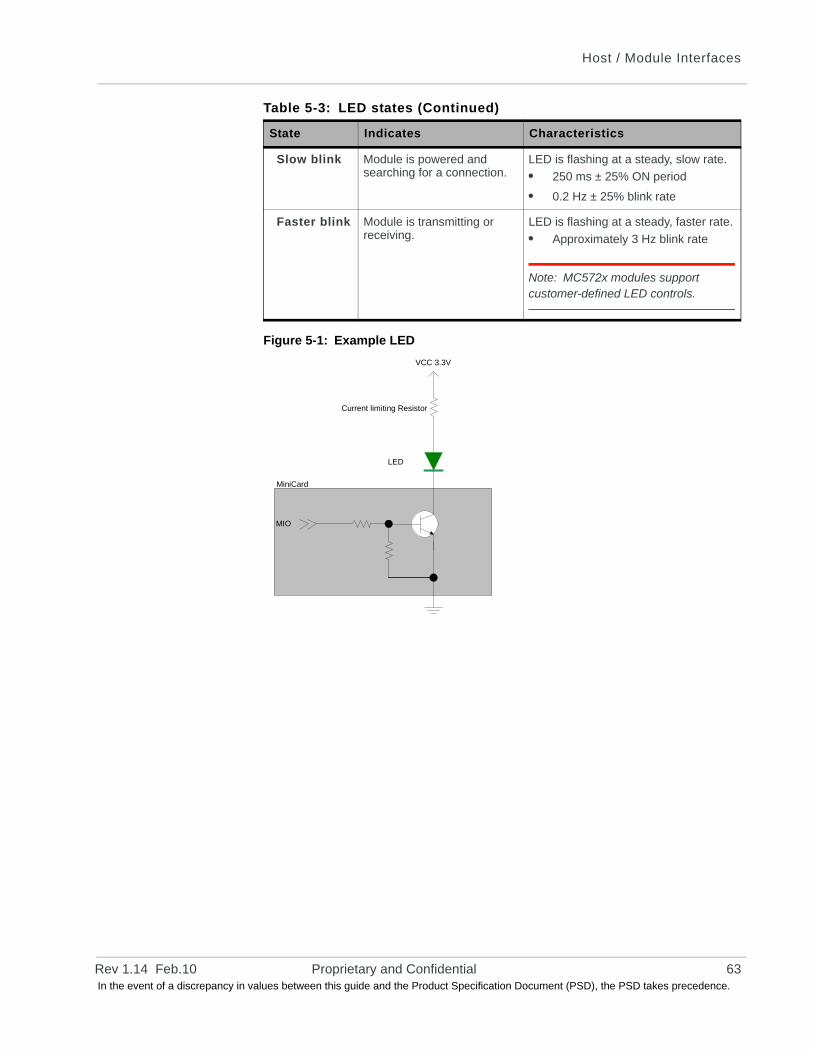
Host / Module Interfaces
Figure 5-1: Example LED
Slow blink Module is powered and searching for a connection.
LED is flashing at a steady, slow rate.
• 250 ms ± 25% ON period
• 0.2 Hz ± 25% blink rate
Faster blink Module is transmitting or receiving.
LED is flashing at a steady, faster rate.
• Approximately 3 Hz blink rate
Note: MC572x modules support customer-defined LED controls.
Table 5-3: LED states (Continued)
State Indicates Characteristics
Current limiting Resistor
LED
VCC 3.3V
MIO
MiniCard
Rev 1.14 Feb.10 Proprietary and Confidential 63 In the event of a discrepancy in values between this guide and the Product Specification Document (PSD), the PSD takes precedence.
CDMA and GSM / UMTS Mini Card Hardware Integration Guide
USIM interface
Note: This section applies only to GSM (MC87xx) modules.
The module is designed to support one USIM (Universal Subscriber Identity Module). The USIM holds account information, allowing users to use their account on multiple devices.
The USIM interface has four signals (plus Ground). These are defined in Table 5-4 (below) with an example circuit shown in Figure 5-2. (For USIM card contacts, see Figure 5-3.)
Table 5-4: USIM pins
Pin name USIM contact number Function
XIM_VCC 1 USIM VCC
XIM_RESET 2 Active low USIM reset
XIM_CLK 3 Serial clock for USIM data
XIM_DATA 7 Bi-directional USIM data line
XIM_GND 5 Ground
64 Proprietary and Confidential 2130114 In the event of a discrepancy in values between this guide and the Product Specification Document (PSD), the PSD takes precedence.
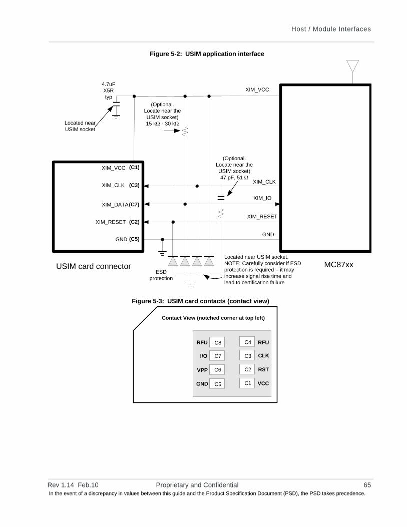
Host / Module Interfaces
Figure 5-2: USIM application interface
Figure 5-3: USIM card contacts (contact view)
MC87xx
XIM_VCC
XIM_RESET
XIM_DATA
XIM_CLK
USIM card connector
GND
(Optional. Locate near the USIM socket)47 pF, 51
4.7uFX5Rtyp
(C1)
XIM_VCC
XIM_CLK
XIM_IO
XIM_RESET
Located near USIM socket
Located near USIM socket.NOTE: Carefully consider if ESD protection is required – it may increase signal rise time and lead to certification failure
GND
ESD protection
(C3)
(C7)
(C2)
(C5)
(Optional. Locate near the USIM socket)15 k - 30 k
C8
C7
C6
C5
C4
C3
C2
C1GND VCC
VPP RST
I/O CLK
RFU RFU
Contact View (notched corner at top left)
Rev 1.14 Feb.10 Proprietary and Confidential 65 In the event of a discrepancy in values between this guide and the Product Specification Document (PSD), the PSD takes precedence.
CDMA and GSM / UMTS Mini Card Hardware Integration Guide
USIM operation
Note: For interface design requirements, refer to:(2G) 3GPP TS 51.010-1, section 27.17, or(3G) ETSI TS 102 230 V5.5.0, section 5.2
When designing the remote USIM interface, you must make sure that the USIM signal integrity is not compromised. Some design recommendations include:
• The total impedance of the VCC and GND connections to the USIM, measured at the module connector, should be less than 1 to minimize voltage drop (includes any trace impedance and lumped element compo-nents — inductors, filters, etc.).
Note: The MC87xx is designed for use with either a 1.8 V or 3 V USIM.
• Position the USIM connector no more than 10 cm from the module. If a longer distance is required because of the design of the host device, a shielded wire assembly is recommended—connect one end as close as possible to the USIM connector and the other end as close as possible to the module connector. The shielded assembly may help shield the USIM interface from system noise.
• Reduce crosstalk on the XIM_data line to reduce the risk of failures during GCF approval testing.
• Avoid routing the XIM_CLK and XIM_DATA lines in parallel over distances greater than 2 cm—cross-coupling of these lines can cause failures.
• Keep USIM signals as short as possible, and keep very low capacitance traces on the XIM_DATA and XIM_CLK signals to minimize signal rise time—signal rise time must be <1 µs. High capacitance increases signal rise time, potentially causing your device to fail certification tests.
• Add external pull-up resistors (15 k — 30 k), if required, between the SIM_IO and SIM_VCC lines to optimize the signal rise time.
• 3GPP has stringent requirements for I/O rise time (<1 µs), signal level limits, and noise immunity—consider this carefully when developing your PCB layout.
• The VCC line should be decoupled close to the USIM socket.
• USIM is specified to run up to 5 MHz (USIM clock rate). Take note of this speed in the placement and routing of the USIM signals and connectors.
• You must decide if, and how much, additional ESD protection and series resistors are suitable for your product. The MC87xx already includes additional ESD protection. Adding more protection (additional circuits) than is necessary could decrease signal rise time, increase load impedance, and cause USIM certification failure.
• Putting an optional decoupling capacitor at XIM_VCC near the USIM socket is recommended—the longer the trace length (impedance) from the socket to the module, the greater the capacitance requirement to meet compliance tests.
• Putting an optional series capacitor and resistor termination (to ground) at XIM_CLK at the USIM socket to reduce EMI and increase signal integrity is recommended if the trace length between the USIM socket and module is long—47 pF and 50 resistor are recommended.
• Protect the USIM socket to make sure that the USIM cannot be removed while the module / host device is powered up. For example, you could place
66 Proprietary and Confidential 2130114 In the event of a discrepancy in values between this guide and the Product Specification Document (PSD), the PSD takes precedence.
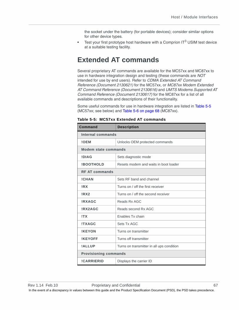
Host / Module Interfaces
the socket under the battery (for portable devices); consider similar options for other device types.
• Test your first prototype host hardware with a Comprion IT3 USIM test device at a suitable testing facility.
Extended AT commands
Several proprietary AT commands are available for the MC57xx and MC87xx to use in hardware integration design and testing (these commands are NOT intended for use by end users). Refer to CDMA Extended AT Command Reference (Document 2130621) for the MC57xx, or MC87xx Modem Extended AT Command Reference (Document 2130616) and UMTS Modems Supported AT Command Reference (Document 2130617) for the MC87xx for a list of all available commands and descriptions of their functionality.
Some useful commands for use in hardware integration are listed in Table 5-5 (MC57xx; see below) and Table 5-6 on page 68 (MC87xx).
Table 5-5: MC57xx Extended AT commands
Command Description
Internal commands
!OEM Unlocks OEM protected commands
Modem state commands
!DIAG Sets diagnostic mode
!BOOTHOLD Resets modem and waits in boot loader
RF AT commands
!CHAN Sets RF band and channel
!RX Turns on / off the first receiver
!RX2 Turns on / off the second receiver
!RXAGC Reads Rx AGC
!RX2AGC Reads second Rx AGC
!TX Enables Tx chain
!TXAGC Sets Tx AGC
!KEYON Turns on transmitter
!KEYOFF Turns off transmitter
!ALLUP Turns on transmitter in all ups condition
Provisioning commands
!CARRIERID Displays the carrier ID
Rev 1.14 Feb.10 Proprietary and Confidential 67 In the event of a discrepancy in values between this guide and the Product Specification Document (PSD), the PSD takes precedence.
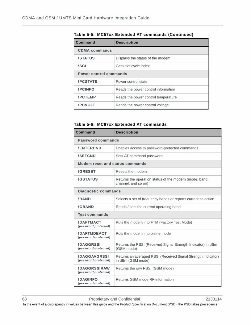
CDMA and GSM / UMTS Mini Card Hardware Integration Guide
CDMA commands
!STATUS Displays the status of the modem
!SCI Gets slot cycle index
Power control commands
!PCSTATE Power control state
!PCINFO Reads the power control information
!PCTEMP Reads the power control temperature
!PCVOLT Reads the power control voltage
Table 5-6: MC87xx Extended AT commands
Command Description
Password commands
!ENTERCND Enables access to password-protected commands
!SETCND Sets AT command password
Modem reset and status commands
!GRESET Resets the modem
!GSTATUS Returns the operation status of the modem (mode, band, channel, and so on)
Diagnostic commands
!BAND Selects a set of frequency bands or reports current selection
!GBAND Reads / sets the current operating band
Test commands
!DAFTMACT(password protected)
Puts the modem into FTM (Factory Test Mode)
!DAFTMDEACT(password-protected)
Puts the modem into online mode
!DAGGRSSI(password-protected)
Returns the RSSI (Received Signal Strength Indicator) in dBm (GSM mode)
!DAGGAVGRSSI(password-protected)
Returns an averaged RSSI (Received Signal Strength Indicator) in dBm (GSM mode)
!DAGGRSSIRAW(password-protected)
Returns the raw RSSI (GSM mode)
!DAGINFO(password-protected)
Returns GSM mode RF information
Table 5-5: MC57xx Extended AT commands (Continued)
Command Description
68 Proprietary and Confidential 2130114 In the event of a discrepancy in values between this guide and the Product Specification Document (PSD), the PSD takes precedence.
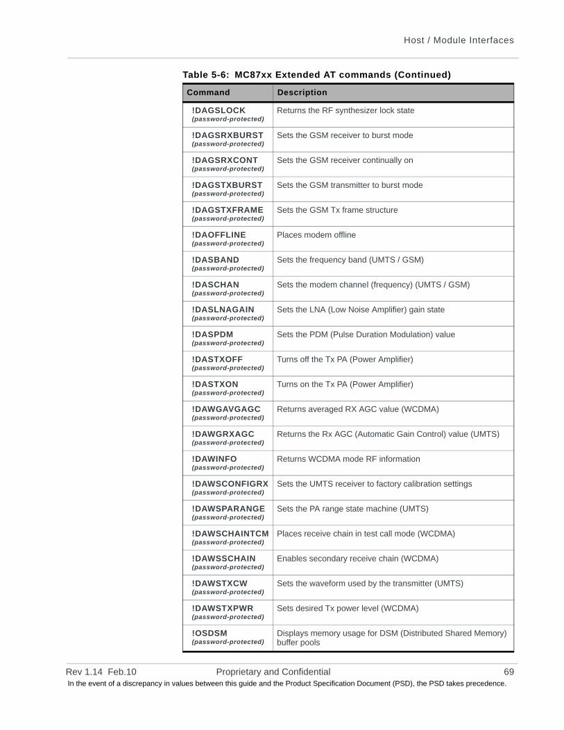
Host / Module Interfaces
!DAGSLOCK(password-protected)
Returns the RF synthesizer lock state
!DAGSRXBURST(password-protected)
Sets the GSM receiver to burst mode
!DAGSRXCONT(password-protected)
Sets the GSM receiver continually on
!DAGSTXBURST(password-protected)
Sets the GSM transmitter to burst mode
!DAGSTXFRAME(password-protected)
Sets the GSM Tx frame structure
!DAOFFLINE(password-protected)
Places modem offline
!DASBAND(password-protected)
Sets the frequency band (UMTS / GSM)
!DASCHAN(password-protected)
Sets the modem channel (frequency) (UMTS / GSM)
!DASLNAGAIN(password-protected)
Sets the LNA (Low Noise Amplifier) gain state
!DASPDM(password-protected)
Sets the PDM (Pulse Duration Modulation) value
!DASTXOFF(password-protected)
Turns off the Tx PA (Power Amplifier)
!DASTXON(password-protected)
Turns on the Tx PA (Power Amplifier)
!DAWGAVGAGC(password-protected)
Returns averaged RX AGC value (WCDMA)
!DAWGRXAGC(password-protected)
Returns the Rx AGC (Automatic Gain Control) value (UMTS)
!DAWINFO(password-protected)
Returns WCDMA mode RF information
!DAWSCONFIGRX(password-protected)
Sets the UMTS receiver to factory calibration settings
!DAWSPARANGE(password-protected)
Sets the PA range state machine (UMTS)
!DAWSCHAINTCM(password-protected)
Places receive chain in test call mode (WCDMA)
!DAWSSCHAIN(password-protected)
Enables secondary receive chain (WCDMA)
!DAWSTXCW(password-protected)
Sets the waveform used by the transmitter (UMTS)
!DAWSTXPWR(password-protected)
Sets desired Tx power level (WCDMA)
!OSDSM(password-protected)
Displays memory usage for DSM (Distributed Shared Memory) buffer pools
Table 5-6: MC87xx Extended AT commands (Continued)
Command Description
Rev 1.14 Feb.10 Proprietary and Confidential 69 In the event of a discrepancy in values between this guide and the Product Specification Document (PSD), the PSD takes precedence.

CDMA and GSM / UMTS Mini Card Hardware Integration Guide
70 Proprietary and Confidential 2130114 In the event of a discrepancy in values between this guide and the Product Specification Document (PSD), the PSD takes precedence.
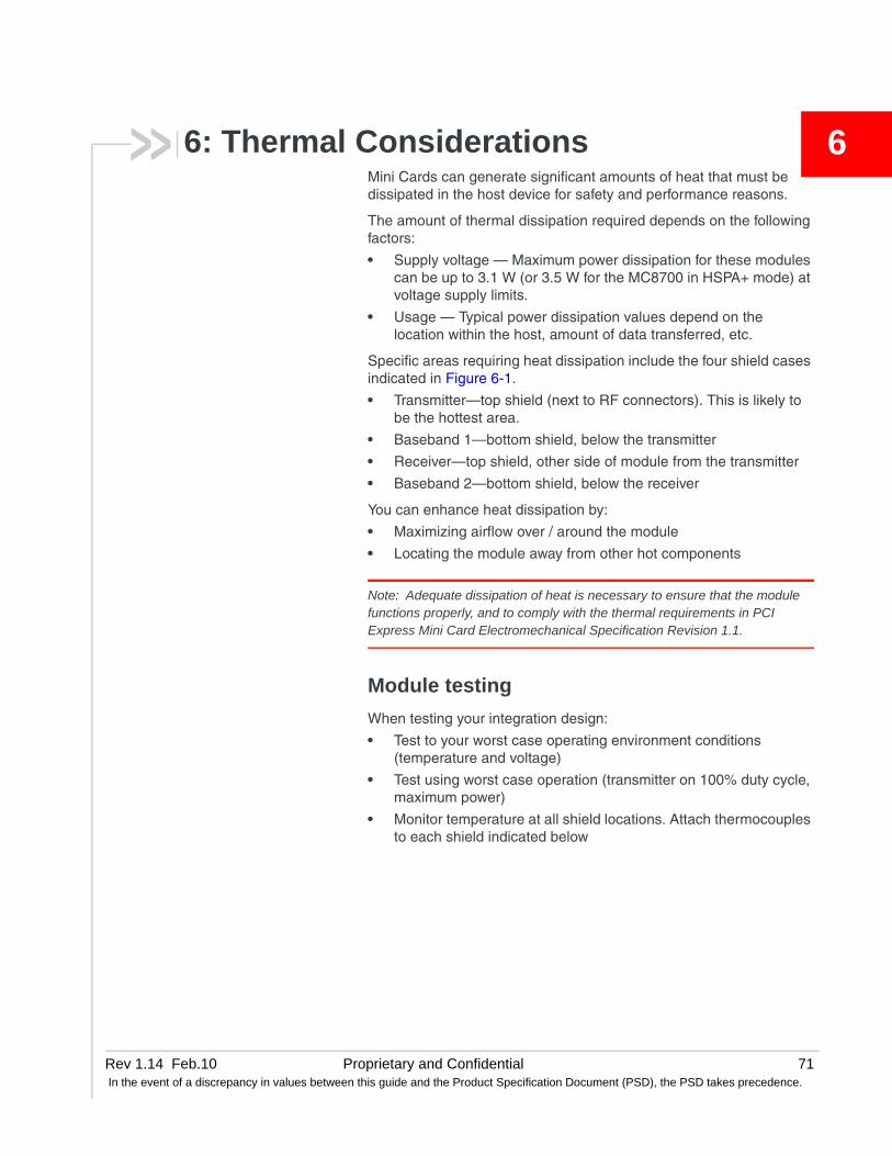
Rev 1.14 In the event
66: Thermal ConsiderationsMini Cards can generate significant amounts of heat that must be dissipated in the host device for safety and performance reasons.
The amount of thermal dissipation required depends on the following factors:
• Supply voltage — Maximum power dissipation for these modules can be up to 3.1 W (or 3.5 W for the MC8700 in HSPA+ mode) at voltage supply limits.
• Usage — Typical power dissipation values depend on the location within the host, amount of data transferred, etc.
Specific areas requiring heat dissipation include the four shield cases indicated in Figure 6-1.
• Transmitter—top shield (next to RF connectors). This is likely to be the hottest area.
• Baseband 1—bottom shield, below the transmitter
• Receiver—top shield, other side of module from the transmitter
• Baseband 2—bottom shield, below the receiver
You can enhance heat dissipation by:
• Maximizing airflow over / around the module
• Locating the module away from other hot components
Note: Adequate dissipation of heat is necessary to ensure that the module functions properly, and to comply with the thermal requirements in PCI Express Mini Card Electromechanical Specification Revision 1.1.
Module testing
When testing your integration design:
• Test to your worst case operating environment conditions (temperature and voltage)
• Test using worst case operation (transmitter on 100% duty cycle, maximum power)
• Monitor temperature at all shield locations. Attach thermocouples to each shield indicated below
Feb.10 Proprietary and Confidential 71of a discrepancy in values between this guide and the Product Specification Document (PSD), the PSD takes precedence.
CDMA and GSM / UMTS Mini Card Hardware Integration Guide
Figure 6-1: Shield locations
Note: Make sure that your system design provides sufficient cooling for the module. The RF shield temperature should be kept below 90 °C when integrated to prevent damage to the module’s components.
72 Proprietary and Confidential 2130114 In the event of a discrepancy in values between this guide and the Product Specification Document (PSD), the PSD takes precedence.
Rev 1.14 In the event
77: Design ChecklistThis chapter provides a summary of the design considerations mentioned throughout this guide. This includes items relating to the power interface, RF integration, thermal considerations, cabling issues, and so on.
Note: This is NOT an exhaustive list of design considerations. It is expected that you will employ good design practices and engineering principles in your integration.
Table 7-1: Hardware integration design considerations
Suggestion Section where discussed
Component placement
Protect the USIM socket so that the USIM cannot be removed while the host is powered up.
USIM operationpage 66
If an ESD suppressor is not used, allow space on the USIM connector for series resistors in layout (up to 100 may be used depending on ESD testing requirements).
USIM operationpage 66
Minimize RF cable losses as these affect the performance values listed in the product specification document.
RF connectionpage 39
Antennas
Match the module / antenna coax connections to 50 W — mismatched antenna impedance and cable loss negatively affects RF performance.
RF connectionpage 39
If installing both the MC57xx and MC87xx in the same device, consider using separate antennas for maximum performance.
Antenna and cablingpage 40
Power
Limit host power rail dips caused by module inrush current by adding sufficient capacitance to the host power rail.
Inrush currentspage 24
Make sure the power supply can handle the maximum current specified for the module type.
Current consumption overviewpage 27
Limit the total impedance of VCC and GND connections to the USIM at the connector to less than 1 W (including any trace impedance and lumped element components — inductors, filters, etc.). All other lines must have a trace impedance less than 2 W.
USIM operationpage 66
Decouple the VCC line close to the USIM socket. The longer the trace length (impedance) from socket to module, the greater the capacitance requirement to meet compliance tests.
USIM operationpage 66
Feb.10 Proprietary and Confidential 73of a discrepancy in values between this guide and the Product Specification Document (PSD), the PSD takes precedence.
CDMA and GSM / UMTS Mini Card Hardware Integration Guide
EMI / ESD
Investigate sources of localized interference early in the design cycle.
Methods to mitigate decreased Rx performancepage 42
Provide ESD protection for the USIM connector at the exposed contact point (in particular, the CLK, VCC, IO, and RESET lines).
USIM operationpage 66
Keep very low capacitance traces on the XIM_DATA and XIM_CLK signals.
To minimize noise leakage, establish a very good ground connection between the module and host.
Ground connectionpage 40
Route cables away from noise sources (for example, power supplies, LCD assemblies, etc.).
Methods to mitigate decreased Rx performancepage 42
Shield high RF-emitting components of the host device (for example, main processor, parallel bus, etc.).
Methods to mitigate decreased Rx performancepage 42
Use discrete filtering on low frequency lines to filter out unwanted high-order harmonic energy.
Methods to mitigate decreased Rx performancepage 42
Use multi-layer PCBs to form shielding layers around high-speed clock traces.
Methods to mitigate decreased Rx performancepage 42
Thermal
Test to worst case operating conditions — temperature, voltage, and operation mode (transmitter on 100% duty cycle, maximum power).
Thermal Considerationspage 71
Use appropriate techniques to reduce module temperatures. (airflow, heat sinks, heat-relief tape, module placement, etc.)
Thermal Considerationspage 71
Host / Modem communication
Make sure the host USB driver supports remote wakeup, resume, and suspend operations, and serial port emulation.
USB handshakingpage 61
When no valid data is being sent, do not send SOF tokens from the host (causes unnecessary power consumption).
USB handshakingpage 61
Table 7-1: Hardware integration design considerations (Continued)
Suggestion Section where discussed
74 Proprietary and Confidential 2130114 In the event of a discrepancy in values between this guide and the Product Specification Document (PSD), the PSD takes precedence.
Rev 1.14 In the event
88: TestingNote: All Sierra Wireless embedded modules are factory-tested to ensure they conform to published product specifications.
Developers of OEM devices integrating Sierra Wireless modules should include a series of test phases in their manufacturing process to make sure that their devices work properly with the embedded modules.
Suggested phases include:
• Acceptance testing—testing of modules when they are received from Sierra Wireless
• Certification testing—testing of completed devices to obtain required certifications before beginning mass production
• Production testing—testing of completed devices with the modules embedded
• Quality assurance testing—post-production
AT command entry timing requirement
Some commands require time to process before additional commands are entered. For example, the modem will return “OK” when it receives AT!DAFTMACT. If AT!DASBAND is received too soon after this, the modem will return an error.
When building automated test scripts, ensure that sufficient delays are embedded where necessary to avoid these errors.
Acceptance testing
Note: Acceptance testing is typically performed for each shipment received.
When you receive a shipment from Sierra Wireless, you should make sure it is suitable before beginning production.
From a random sampling of units, test that:
• The units are operational
• The units are loaded with the correct firmware version
Test requirements
To perform the suggested tests, you require a test system in which to temporarily install the module, and you must be able to observe the test device’s LED indicator.
Feb.10 Proprietary and Confidential 75of a discrepancy in values between this guide and the Product Specification Document (PSD), the PSD takes precedence.
CDMA and GSM / UMTS Mini Card Hardware Integration Guide
Test procedure
The following is a suggested acceptance testing procedure using Sierra Wireless’ Watcher software:
Note: You can perform these tests using appro-priate AT commands.
Test 1: Check power-up and initialization
1. After installing the module, start the test system.
2. Launch Watcher.
3. Check the LED—if the LED is off, there is a problem with the module or with the connection to the LED.
Test 2: Check version numbers
1. From Watcher, select Help > About.
2. Verify that the firmware version in the About window is correct.
3. Close the About window.
If the module fails either of these tests, or is not recognized by Watcher:
1. Replace the module with one that is known to work correctly and repeat the tests.
2. If the tests are successful, reinstall the original module and repeat the tests.
If the module still does not work correctly, contact your account manager.
Certification testing
Note: Typically, you need to pass certification testing of your device with the integrated module one time only.
When you produce a host device with an embedded Sierra Wireless module, you must obtain certifications for the final product from appropriate regulatory bodies in the jurisdictions where it will be distributed.
Note: The module itself (MC57xx, MC87xx) has been certified already—only the integrated device needs certification.
The following are some of the regulatory bodies from which you may require certification—it is your responsibility to make sure that you obtain all necessary certifications for your product from these or other groups:
• FCC (Federal Communications Commission—www.fcc.gov)
• Industry Canada (www.ic.gc.ca)
• CSA (Canadian Standards Association—www.csa.ca)
• Factory Mutual (FM Global—www.allendale.com)
• Underwriters Laboratories Inc. (www.ul.com)
• (MC57xx only) CDG (CDMA Development Group—www.cdg.org)
• (MC87xx only) GCF (Global Certification Forum—gcf.gsm.org) outside of North America
76 Proprietary and Confidential 2130114 In the event of a discrepancy in values between this guide and the Product Specification Document (PSD), the PSD takes precedence.
Testing
• (MC87xx only) PTCRB (PCS Type Certification Review Board—www.ptcrb.com) in North America
Production testing
Note: Production testing typically continues for the life of the product.
Each assembled device should be tested to make sure the module is installed correctly and is functioning within normal operating parameters.
Note: All Sierra Wireless embedded modules are fully factory-tested to ensure they conform to published product specifications.
In general, production testing ensures that the module is installed correctly (I/O signals are passed between the host and module), and the antenna is connected and performing to specifications (RF tests).
Typical items to test include host connectivity, the RF assembly (Tx and/or Rx, as appropriate), and the audio assembly (for voice-enabled modules).
Note: The amount and types of tests to perform are your decision—the tests listed in this section are guidelines only. Make sure that the tests you perform exercise functionality to the degree that your situation requires—this may include, for example, testing network availability, any host device configuration issues, baseband testing (GPIO / Audio, host / module connectors) and appropriate RF testing (Tx and/or Rx).
Use an appropriate test station for your testing environment (see Test requirements on page 75 for suggestions) and use AT commands to control the integrated module.
Note: Your test location must be protected from ESD to avoid interference with the module and antenna(s) (assuming that your test computer is in a disassembled state).
Also, consider using an RF shielding box as shown in the suggested test equipment—local government regulations may prohibit unauthorized transmissions.
Suggested manual functional test procedure
This section presents a procedure for performing a basic manual functional test on a laboratory bench using the Mini Card and a Mini Card Dev Kit. When you have become familiar with the testing method, use it to develop your own automated production testing procedures.
Rev 1.14 Feb.10 Proprietary and Confidential 77 In the event of a discrepancy in values between this guide and the Product Specification Document (PSD), the PSD takes precedence.
CDMA and GSM / UMTS Mini Card Hardware Integration Guide
Suggested tests
Consider the following tests when you design your production test procedures for devices with the MC57xx and/or MC87xx installed.
• Visual check of the module’s connectors, RF assemblies, and audio assem-blies (if applicable)
• Module is operational
• USB connection is functional
• LED is functional• W_Disable# (module power down)
• Firmware revision check
• Rx tests on main and auxiliary paths
• Tx test
• Audio (microphone and speaker) tests (for voice-enabled modules)
Suggested test plan procedure
Note: The following is a suggested outline for a relatively comprehensive test plan—you must decide which tests are appropriate for your product.This is not an exhaustive list of tests—you may wish to add additional tests that more fully exercise the capabilities of your product.
Note: You may choose to create and run a test program that automates portions of the test procedure.
Using an appropriate Dev Kit-based test station (a suggested setup is described in Suggested testing equipment on page 93), and referring to the appropriate standard and extended AT command references:
1. Visually inspect the module’s connectors and RF assemblies for obvious defects before installing it in the test station.
Note: To power-off the module, drive W_Disable# low for the required minimum period. See State change: Power off / on on page 23 for details.
2. Ensure that the module is turned off before beginning your tests (set W_Disable# low).
3. If using Linux, determine if any USB devices are currently connected to the computer:
a. Open a shell window and enter the command ls /dev/tty/USB*.
b. Record the ttyUSBn values that are returned; these are the currently connected USB devices. If the command returns “no such file or directory”, there are no devices currently connected.
4. Test W_Disable#—Turn on the module by letting W_Disable# float (high impedance). Depending on your device, this may just require powering up the device. Refer to the PCI Express Mini Card Dev Kit Quick Start Guide (Document 2130705) for more details.
5. Test USB functionality—Check for USB enumeration.
78 Proprietary and Confidential 2130114 In the event of a discrepancy in values between this guide and the Product Specification Document (PSD), the PSD takes precedence.
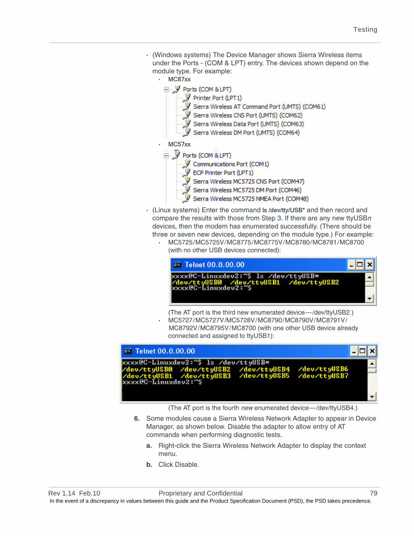
Testing
· (Windows systems) The Device Manager shows Sierra Wireless items under the Ports - (COM & LPT) entry. The devices shown depend on the module type. For example:
· MC87xx
· MC57xx
· (Linux systems) Enter the command ls /dev/tty/USB* and then record and compare the results with those from Step 3. If there are any new ttyUSBn devices, then the modem has enumerated successfully. (There should be three or seven new devices, depending on the module type.) For example:
· MC5725/MC5725V/MC8775/MC8775V/MC8780/MC8781/MC8700 (with no other USB devices connected):
(The AT port is the third new enumerated device—/dev/ttyUSB2.)· MC5727/MC5727V/MC5728V/MC8790/MC8790V/MC8791V/
MC8792V/MC8795V/MC8700 (with one other USB device already connected and assigned to ttyUSB1):
(The AT port is the fourth new enumerated device—/dev/ttyUSB4.)
6. Some modules cause a Sierra Wireless Network Adapter to appear in Device Manager, as shown below. Disable the adapter to allow entry of AT commands when performing diagnostic tests.
a. Right-click the Sierra Wireless Network Adapter to display the context menu.
b. Click Disable.
Rev 1.14 Feb.10 Proprietary and Confidential 79 In the event of a discrepancy in values between this guide and the Product Specification Document (PSD), the PSD takes precedence.
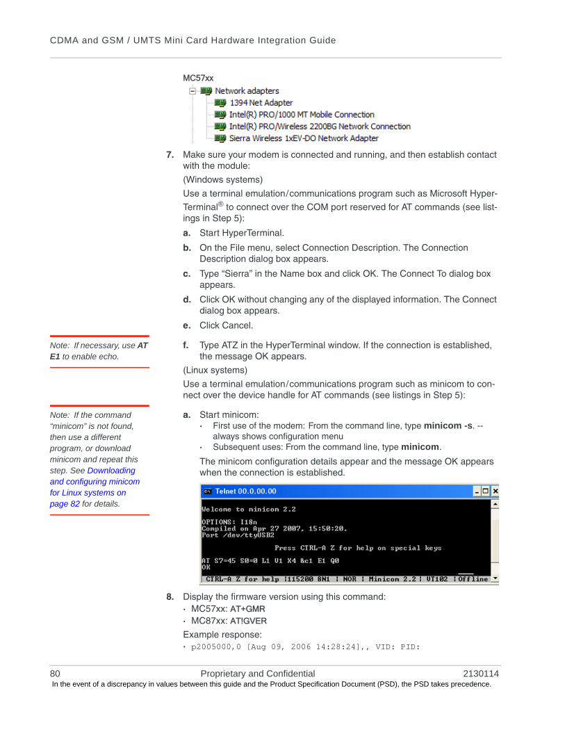
CDMA and GSM / UMTS Mini Card Hardware Integration Guide
MC57xx
7. Make sure your modem is connected and running, and then establish contact with the module:
(Windows systems)
Use a terminal emulation/communications program such as Microsoft Hyper-
Terminal® to connect over the COM port reserved for AT commands (see list-ings in Step 5):
a. Start HyperTerminal.
b. On the File menu, select Connection Description. The Connection Description dialog box appears.
c. Type “Sierra” in the Name box and click OK. The Connect To dialog box appears.
d. Click OK without changing any of the displayed information. The Connect dialog box appears.
e. Click Cancel.
Note: If necessary, use AT E1 to enable echo.
f. Type ATZ in the HyperTerminal window. If the connection is established, the message OK appears.
(Linux systems)
Use a terminal emulation/communications program such as minicom to con-nect over the device handle for AT commands (see listings in Step 5):
Note: If the command “minicom” is not found, then use a different program, or download minicom and repeat this step. See Downloading and configuring minicom for Linux systems on page 82 for details.
a. Start minicom:· First use of the modem: From the command line, type minicom -s. --
always shows configuration menu· Subsequent uses: From the command line, type minicom.
The minicom configuration details appear and the message OK appears when the connection is established.
8. Display the firmware version using this command:· MC57xx: AT+GMR
· MC87xx: AT!GVER
Example response:· p2005000,0 [Aug 09, 2006 14:28:24],, VID: PID:
80 Proprietary and Confidential 2130114 In the event of a discrepancy in values between this guide and the Product Specification Document (PSD), the PSD takes precedence.
Testing
Characters 5–6 are the firmware version (50 in this example).
9. Test the LED—Set the LED in blinking mode using this command, then visually verify that the LED turns off and on:· MC57xx: AT!LED=0,1
· MC87xx: AT!DLED or AT!LEDCTRL
10. Unlock the extended AT command set, using:· MC57xx: AT!OEM=176
· MC87xx: AT!ENTERCND
11. Put the module in diagnostic / factory test mode using:· MC57xx: AT!DIAG
· MC87xx: AT!DAFTMACT
12. (MC87xx only) Communicate with the USIM using +CPIN or +CIMI.
Note: When performing RF tests, use a test platform similar to those shown in Figure 8-2 (page 94) and Figure 8-3 (page 95).
13. Test RF transmission, if desired:· MC57xx—See Testing RF transmission path—MC57xx on page 82.· MC87xx—See Testing RF transmission path—MC87xx on page 84.
14. Test RF reception, if desired:· MC57xx—See Testing RF Receive path—MC57xx on page 86.· MC87xx— See Testing RF Receive path—MC87xx on page 87.
Note: The GPS receiver does not need to be tested for UMTS (MC878x) or CDMA (MC57xx) modules supporting diversity because RF connectivity is validated by testing the diversity receiver in Step 14.
15. (MC8775V only) Test the GPS receiver, if desired. See Testing GPS Receiver—MC8775V on page 90.
16. Test Audio loop-back. See Test Audio Loop-back—MC5725V / MC5727V / MC5728V / MC8775V / MC8790V / MC8791V / MC8792V / MC8795V on page 91.
17. Finish testing
a. If the network adapter was disabled in Step 6, re-enable it (same instruc-tions, except click Enable instead of Disable).
Note: To power-off the module, drive W_Disable# low for the required minimum period. See State change: Power off / on on page 23 for details.
b. Set the W_Disable# signal low and confirm that the module powers down:· Windows systems—The Sierra Wireless items under the Ports (COM &
LPT) entry in Device Manager disappear as the module powers off.· Linux systems—Enter the command ls /dev/tty/USB*. The devices
enumerated in Step 5 will not appear after the module powers off.
Rev 1.14 Feb.10 Proprietary and Confidential 81 In the event of a discrepancy in values between this guide and the Product Specification Document (PSD), the PSD takes precedence.
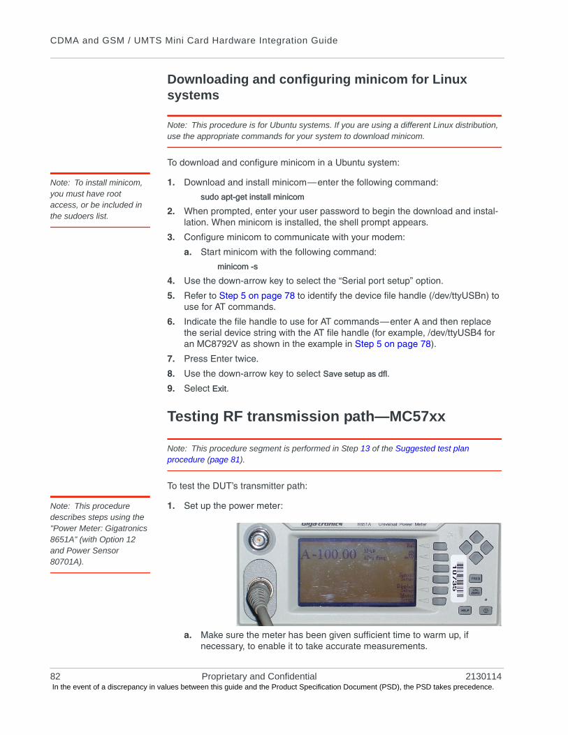
CDMA and GSM / UMTS Mini Card Hardware Integration Guide
Downloading and configuring minicom for Linux systems
Note: This procedure is for Ubuntu systems. If you are using a different Linux distribution, use the appropriate commands for your system to download minicom.
To download and configure minicom in a Ubuntu system:
Note: To install minicom, you must have root access, or be included in the sudoers list.
1. Download and install minicom—enter the following command:
sudo apt-get install minicom
2. When prompted, enter your user password to begin the download and instal-lation. When minicom is installed, the shell prompt appears.
3. Configure minicom to communicate with your modem:
a. Start minicom with the following command:
minicom -s
4. Use the down-arrow key to select the “Serial port setup” option.
5. Refer to Step 5 on page 78 to identify the device file handle (/dev/ttyUSBn) to use for AT commands.
6. Indicate the file handle to use for AT commands—enter A and then replace the serial device string with the AT file handle (for example, /dev/ttyUSB4 for an MC8792V as shown in the example in Step 5 on page 78).
7. Press Enter twice.
8. Use the down-arrow key to select Save setup as dfl.
9. Select Exit.
Testing RF transmission path—MC57xx
Note: This procedure segment is performed in Step 13 of the Suggested test plan procedure (page 81).
To test the DUT’s transmitter path:
Note: This procedure describes steps using the "Power Meter: Gigatronics 8651A” (with Option 12 and Power Sensor 80701A).
1. Set up the power meter:
a. Make sure the meter has been given sufficient time to warm up, if necessary, to enable it to take accurate measurements.
82 Proprietary and Confidential 2130114 In the event of a discrepancy in values between this guide and the Product Specification Document (PSD), the PSD takes precedence.
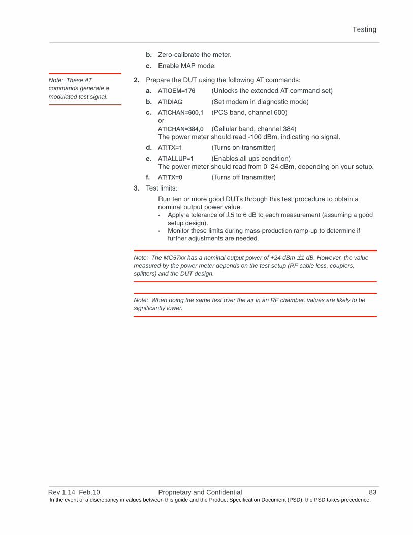
Testing
b. Zero-calibrate the meter.
c. Enable MAP mode.
Note: These AT commands generate a modulated test signal.
2. Prepare the DUT using the following AT commands:
a. AT!OEM=176 (Unlocks the extended AT command set)
b. AT!DIAG (Set modem in diagnostic mode)
c. AT!CHAN=600,1 (PCS band, channel 600)orAT!CHAN=384,0 (Cellular band, channel 384)The power meter should read -100 dBm, indicating no signal.
d. AT!TX=1 (Turns on transmitter)
e. AT!ALLUP=1 (Enables all ups condition)The power meter should read from 0–24 dBm, depending on your setup.
f. AT!TX=0 (Turns off transmitter)
3. Test limits:
Run ten or more good DUTs through this test procedure to obtain a nominal output power value.· Apply a tolerance of 5 to 6 dB to each measurement (assuming a good
setup design).· Monitor these limits during mass-production ramp-up to determine if
further adjustments are needed.
Note: The MC57xx has a nominal output power of +24 dBm 1 dB. However, the value measured by the power meter depends on the test setup (RF cable loss, couplers, splitters) and the DUT design.
Note: When doing the same test over the air in an RF chamber, values are likely to be significantly lower.
Rev 1.14 Feb.10 Proprietary and Confidential 83 In the event of a discrepancy in values between this guide and the Product Specification Document (PSD), the PSD takes precedence.
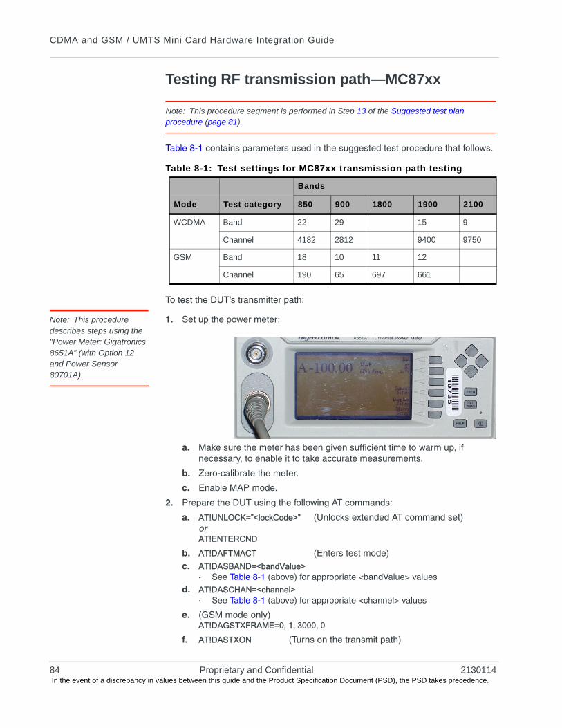
CDMA and GSM / UMTS Mini Card Hardware Integration Guide
Testing RF transmission path—MC87xx
Note: This procedure segment is performed in Step 13 of the Suggested test plan procedure (page 81).
Table 8-1 contains parameters used in the suggested test procedure that follows.
To test the DUT’s transmitter path:
Note: This procedure describes steps using the "Power Meter: Gigatronics 8651A” (with Option 12 and Power Sensor 80701A).
1. Set up the power meter:
a. Make sure the meter has been given sufficient time to warm up, if necessary, to enable it to take accurate measurements.
b. Zero-calibrate the meter.
c. Enable MAP mode.
2. Prepare the DUT using the following AT commands:
a. AT!UNLOCK=”<lockCode>” (Unlocks extended AT command set)orAT!ENTERCND
b. AT!DAFTMACT (Enters test mode)c. AT!DASBAND=<bandValue>
· See Table 8-1 (above) for appropriate <bandValue> values
d. AT!DASCHAN=<channel>· See Table 8-1 (above) for appropriate <channel> values
e. (GSM mode only)AT!DAGSTXFRAME=0, 1, 3000, 0
f. AT!DASTXON (Turns on the transmit path)
Table 8-1: Test settings for MC87xx transmission path testing
Bands
Mode Test category 850 900 1800 1900 2100
WCDMA Band 22 29 15 9
Channel 4182 2812 9400 9750
GSM Band 18 10 11 12
Channel 190 65 697 661
84 Proprietary and Confidential 2130114 In the event of a discrepancy in values between this guide and the Product Specification Document (PSD), the PSD takes precedence.
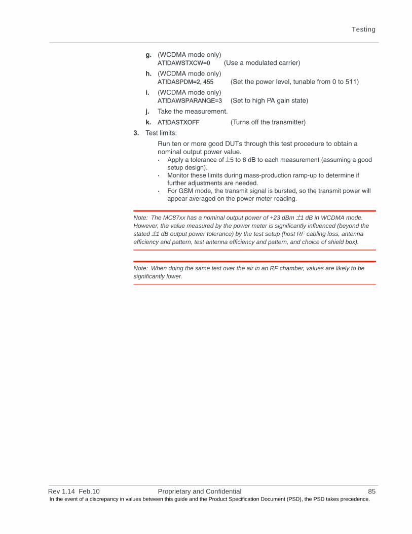
Testing
g. (WCDMA mode only)AT!DAWSTXCW=0 (Use a modulated carrier)
h. (WCDMA mode only)AT!DASPDM=2, 455 (Set the power level, tunable from 0 to 511)
i. (WCDMA mode only)AT!DAWSPARANGE=3 (Set to high PA gain state)
j. Take the measurement.
k. AT!DASTXOFF (Turns off the transmitter)
3. Test limits:
Run ten or more good DUTs through this test procedure to obtain a nominal output power value.· Apply a tolerance of 5 to 6 dB to each measurement (assuming a good
setup design).· Monitor these limits during mass-production ramp-up to determine if
further adjustments are needed.· For GSM mode, the transmit signal is bursted, so the transmit power will
appear averaged on the power meter reading.
Note: The MC87xx has a nominal output power of +23 dBm 1 dB in WCDMA mode. However, the value measured by the power meter is significantly influenced (beyond the stated 1 dB output power tolerance) by the test setup (host RF cabling loss, antenna efficiency and pattern, test antenna efficiency and pattern, and choice of shield box).
Note: When doing the same test over the air in an RF chamber, values are likely to be significantly lower.
Rev 1.14 Feb.10 Proprietary and Confidential 85 In the event of a discrepancy in values between this guide and the Product Specification Document (PSD), the PSD takes precedence.
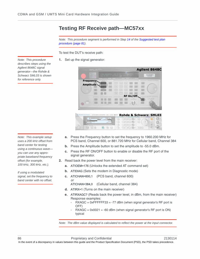
CDMA and GSM / UMTS Mini Card Hardware Integration Guide
Testing RF Receive path—MC57xx
Note: This procedure segment is performed in Step 14 of the Suggested test plan procedure (page 81).
To test the DUT’s receive path:
Note: This procedure describes steps using the Agilent 8648C signal generator—the Rohde & Schwarz SML03 is shown for reference only.
1. Set up the signal generator:
Note: This example setup uses a 200 kHz offset from band center for testing using a continuous wave—you can use any appro-priate baseband frequency offset (for example, 100 kHz, 300 kHz, etc.).
If using a modulated signal, set the frequency to band center with no offset.
a. Press the Frequency button to set the frequency to 1960.200 MHz for PCS band, Channel 600, or 881.720 MHz for Cellular band, Channel 384
b. Press the Amplitude button to set the amplitude to -55.0 dBm.
c. Press the RF ON/OFF button to enable or disable the RF port of the signal generator.
2. Read back the power level from the main receiver:
a. AT!OEM=176 (Unlocks the extended AT command set)
b. AT!DIAG (Sets the modem in Diagnostic mode)
c. AT!CHAN=600,1 (PCS band, channel 600)orAT!CHAN=384,0 (Cellular band, channel 384)
d. AT!RX=1 (Turns on the main receiver)
e. AT!RXAGC? (Reads back the power level, in dBm, from the main receiver)Response examples:· RXAGC = 0xFFFFFF33 = -77 dBm (when signal generator’s RF port is
OFF)· RXAGC = 0x0021 = -60 dBm (when signal generator’s RF port is ON)
typical
Note: The dBm value displayed is calculated to reflect the power at the input connector.
86 Proprietary and Confidential 2130114 In the event of a discrepancy in values between this guide and the Product Specification Document (PSD), the PSD takes precedence.
Testing
f. AT!RX2=1 (Turns on diversity receiver)
g. AT!RX2AGC? (Reads back the power level, in dBm, from the diversity receiver)Response examples:· RX2AGC = 0xFFFFFF76 = -84 dBm (when signal generator’s RF port is
OFF)· RX2AGC = 0xFFFFFFC6 = -69 dBm (when signal generator’s RF port is
ON) typical
h. AT!RX=0 (Turns off main receiver)
i. AT!RX2=0 (Turns off diversity receiver)
3. Test limits
Run ten or more good DUTs through this test procedure to obtain a nominal received power value.· Apply a tolerance of 5 to 6 dB to each measurement (assuming a good
setup design).· Make sure the measurement is made at a high enough level that it is not
influenced by DUT-generated and ambient noise.· The Signal Generator power level should be at least -50 dBm.· Monitor these limits during mass-production ramp-up to determine if
further adjustments are needed.
Note: The value measured by the DUT depends on the test setup and DUT design. Host RF cabling loss, antenna efficiency and pattern, test antenna efficiency and pattern, and choice of shield box all significantly influence the measurement.
Note: When doing the same test over the air in an RF chamber, values are likely to be significantly lower.
Testing RF Receive path—MC87xx
Note: This procedure segment is performed in Step 14 of the Suggested test plan procedure (page 81).
Table 8-2 contains parameters used in the suggested test procedure that follows.
Table 8-2: Test settings for MC87xx Receive path testing
Bands
Mode Test category 850 900 1800 1900 2100
WCDMA Frequencya(MHz) 882.60 948.60 1961.2 2141.2
Band 22 29 15 9
Channel 4182 2812 9400 9750
Rev 1.14 Feb.10 Proprietary and Confidential 87 In the event of a discrepancy in values between this guide and the Product Specification Document (PSD), the PSD takes precedence.
CDMA and GSM / UMTS Mini Card Hardware Integration Guide
To test the DUT’s receive path:
Note: This procedure describes steps using the Agilent 8648C signal generator—the Rohde & Schwarz SML03 is shown for reference only.
1. Set up the signal generator:
a. Set the amplitude to:· -80 dBm (WCDMA mode)· -60 dBm (GSM mode)
b. Set the frequency for the band being tested. See Table 8-2 on page 87 for frequency values.
2. Set up the DUT:
a. AT!UNLOCK=”<customerCode>” or AT!ENTERCND
b. AT!DAFTMACT
c. AT!DASBAND=<band>· See Table 8-2 on page 87 for <band> values
d. AT!DASCHAN=<channel>· See Table 8-2 on page 87 for <channel> values
e. AT!DASLNAGAIN=0 (sets the LNA to maximum gain)
f. (WCDMA mode)
i. AT!DAWGAVGAGC=9400,0 (for PCS1900, channel 9400 as an example)
(GSM mode)
i. AT!DAGSRXBURST=0 (set to receive bursted mode)
GSM Frequencyb(MHz) 881.667 948.067 1842.267 1960.067
Band 18 10 11 12
Channel 190 65 697 661
a. All values offset from actual center channel by +1.2 MHzb. All values offset from actual center channel by +67 kHz
Table 8-2: Test settings for MC87xx Receive path testing (Continued)
Bands
Mode Test category 850 900 1800 1900 2100
88 Proprietary and Confidential 2130114 In the event of a discrepancy in values between this guide and the Product Specification Document (PSD), the PSD takes precedence.
Testing
ii. AT!DAGGAVGRSSI=190,0 (for channel 190, for example)
The returned value is the RSSI in dBm.
3. Test limits:
Run ten or more good DUTs through this test procedure to obtain a nominal received power value.· Apply a tolerance of 5 to 6 dB to each measurement (assuming a good
setup design).· Make sure the measurement is made at a high enough level that it is not
influenced by DUT-generated and ambient noise.· The Signal Generator power level can be adjusted and new limits found if
the radiated test needs greater signal strength.· Monitor these limits during mass-production ramp-up to determine if
further adjustments are needed.
Note: The value measured from the DUT is significantly influenced by the test setup and DUT design (host RF cabling loss, antenna efficiency and pattern, test antenna efficiency and pattern, and choice of shield box).
Note: Diversity is not available in GSM mode.
4. Test diversity paths:· MC8780 (WCDMA 850 / WCDMA 2100)· MC8781 (WCDMA 850 / WCDMA 1900)· MC8790/MC8790V (WCDMA 850 / WCDMA 1900 / WCDMA 2100)· MC8795V/MC8700 (WCDMA 850 / WCDMA 900 / WCDMA 1900 /
WCDMA 2100):
a. Set up the signal generator as in Step 1.
b. Set up the DUT:
Note: Setup of the DUT is the same as in Step 2, except for a change to AT!DAWGAVGAGC and the addition of AT!DAWSS-CHAIN.
i. AT!UNLOCK=”<customerCode>” or AT!ENTERCND
ii. AT!DAFTMACT
iii. AT!DASBAND=<band>· See Table 8-2 on page 87 for <band> values
iv. AT!DAWSSCHAIN=1 (enables the secondary chain)
v. AT!DASCHAN=<channel>· See Table 8-2 on page 87 for <channel> values
vi. AT!DASLNAGAIN=0 (sets the LNA to maximum gain)
vii.AT!DAWGAVGAGC=9400,0,1 (the ‘1’ indicates the diversity path is used)
c. Test the limits as in Step 3.
Rev 1.14 Feb.10 Proprietary and Confidential 89 In the event of a discrepancy in values between this guide and the Product Specification Document (PSD), the PSD takes precedence.

CDMA and GSM / UMTS Mini Card Hardware Integration Guide
Testing GPS Receiver—MC8775V
Note: The GPS receiver does not need to be tested for UMTS (MC878x) or CDMA (MC57xx) modules supporting diversity because RF connectivity is validated by testing the diversity receiver in Step 14 of the Suggested test plan procedure (page 81).
Note: This procedure segment is performed in Step 15 of the Suggested test plan procedure (page 81).
To test the carrier-to-noise level for the GPS receive path:
Note: This procedure describes steps using the Agilent 8648C signal generator—the Rohde & Schwarz SML03 is shown for reference only.
1. Set up the signal generator:
a. Set the amplitude to -110 dBm.
b. Set the frequency to 1575.52 MHz. This is100 kHz above the center frequency for GPS and is needed to accurately measure the carrier-to-noise (C/N) level.
2. Set up the DUT using the following commands:a. AT!UNLOCK=”<customerCode>”
b. AT!DAFTMACT (Puts modem into factory test mode)
c. AT!DAAGCTON (Queries power difference between carrier signal and receiver)
3. Test limits:
Run ten or more good DUTs through this test procedure to obtain averaged C/N readings.· The GPS receiver responds to signal levels from -130 dBm to -80 dBm.· Measure C/N five times for each DUT to obtain an average reading at
-110 dB.· Make sure the C/N is less than 15 dB when the signal generator is off.· Allow for 5 dB of C/N variation to identify any problems in the GPS
receive path.
90 Proprietary and Confidential 2130114 In the event of a discrepancy in values between this guide and the Product Specification Document (PSD), the PSD takes precedence.
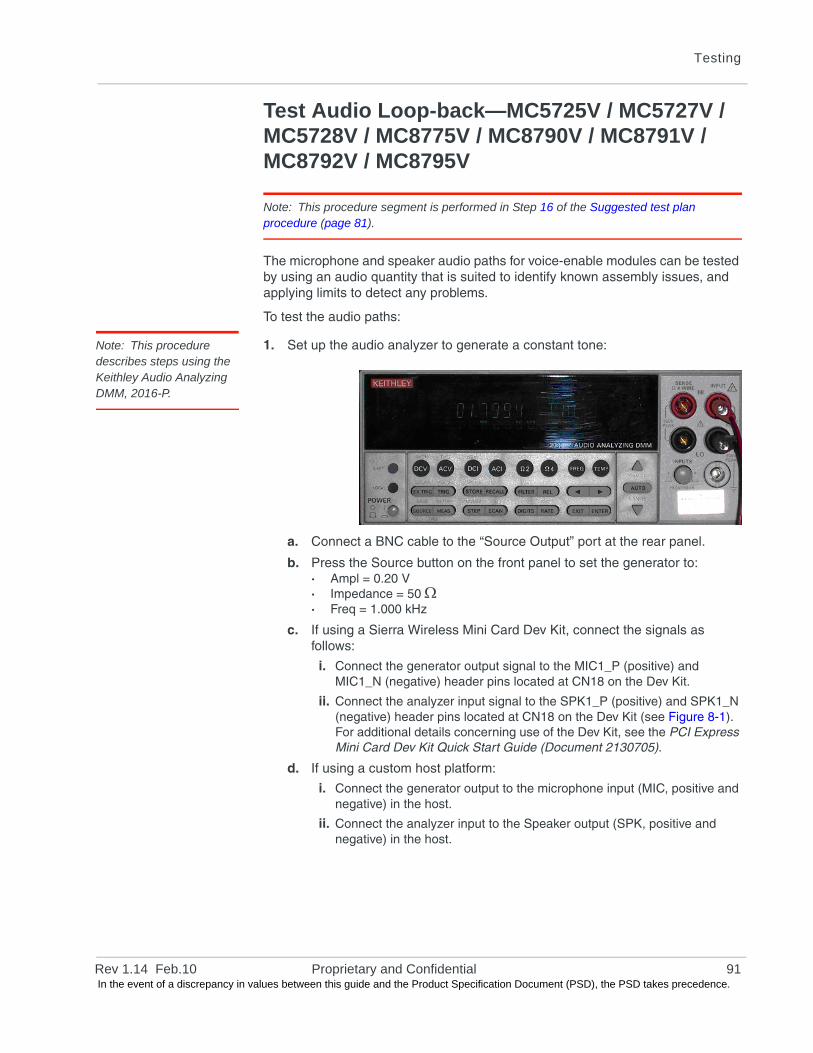
Testing
Test Audio Loop-back—MC5725V / MC5727V / MC5728V / MC8775V / MC8790V / MC8791V / MC8792V / MC8795V
Note: This procedure segment is performed in Step 16 of the Suggested test plan procedure (page 81).
The microphone and speaker audio paths for voice-enable modules can be tested by using an audio quantity that is suited to identify known assembly issues, and applying limits to detect any problems.
To test the audio paths:
Note: This procedure describes steps using the Keithley Audio Analyzing DMM, 2016-P.
1. Set up the audio analyzer to generate a constant tone:
a. Connect a BNC cable to the “Source Output” port at the rear panel.
b. Press the Source button on the front panel to set the generator to:· Ampl = 0.20 V· Impedance = 50 · Freq = 1.000 kHz
c. If using a Sierra Wireless Mini Card Dev Kit, connect the signals as follows:
i. Connect the generator output signal to the MIC1_P (positive) and MIC1_N (negative) header pins located at CN18 on the Dev Kit.
ii. Connect the analyzer input signal to the SPK1_P (positive) and SPK1_N (negative) header pins located at CN18 on the Dev Kit (see Figure 8-1). For additional details concerning use of the Dev Kit, see the PCI Express Mini Card Dev Kit Quick Start Guide (Document 2130705).
d. If using a custom host platform:
i. Connect the generator output to the microphone input (MIC, positive and negative) in the host.
ii. Connect the analyzer input to the Speaker output (SPK, positive and negative) in the host.
Rev 1.14 Feb.10 Proprietary and Confidential 91 In the event of a discrepancy in values between this guide and the Product Specification Document (PSD), the PSD takes precedence.
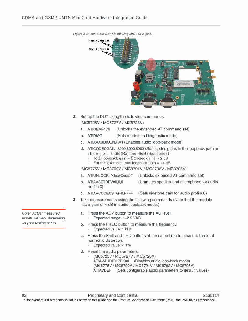
CDMA and GSM / UMTS Mini Card Hardware Integration Guide
Figure 8-1: Mini Card Dev Kit showing MIC / SPK pins.
2. Set up the DUT using the following commands:
(MC5725V / MC5727V / MC5728V)
a. AT!OEM=176 (Unlocks the extended AT command set)
b. AT!DIAG (Sets modem in Diagnostic mode)
c. AT!AVAUDIOLPBK=1 (Enables audio loop-back mode)
d. AT!CODECGAIN=8000,8000,8000 (Sets codec gains in the loopback path to +6 dB (Tx), +6 dB (Rx) and -6dB (SideTone).)· Total loopback gain = (codec gains) - 2 dB· For this example, total loopback gain = +4 dB
(MC8775V / MC8790V / MC8791V / MC8792V / MC8795V)
a. AT!UNLOCK=”<lockCode>” (Unlocks extended AT command set)
b. AT!AVSETDEV=0,0,0 (Unmutes speaker and microphone for audio profile 0)
c. AT!AVCODECSTG=0,FFFF (Sets sidetone gain for audio profile 0)
3. Take measurements using the following commands (Note that the module has a gain of 4 dB in audio loopback mode.)
Note: Actual measured results will vary, depending on your testing setup.
a. Press the ACV button to measure the AC level.· Expected range: 1–2.5 VAC
b. Press the FREQ button to measure the frequency.· Expected value: 1 kHz
c. Press the Shift and THD buttons at the same time to measure the total harmonic distortion.· Expected value: < 1%
d. Reset the audio parameters:· (MC5725V / MC5727V / MC5728V)
AT!AVAUDIOLPBK=0 (Disables audio loop-back mode)· (MC8775V / MC8790V / MC8791V / MC8792V / MC8795V)
AT!AVDEF (Sets configurable audio parameters to default values)
92 Proprietary and Confidential 2130114 In the event of a discrepancy in values between this guide and the Product Specification Document (PSD), the PSD takes precedence.
Testing
Quality assurance testing
Note: QA is an ongoing process based on random samples from a finished batch of devices.
The quality assurance tests that you perform on your finished products should be designed to verify the performance and quality of your devices.
The following are some testing suggestions that can confirm that the antenna is interfaced properly, and the RF module is calibrated and performs to specifications:
• Module registration on cellular networks
• Power consumption
• Originate and terminate data and voice (if applicable) calls
• Cell hand-off
• Transmitter and receiver tests
• FER (Frame Error Rate) as an indicator of receiver sensitivity / performance
• Channel and average power measurements to verify that the device is trans-mitting within product specifications
• RF sensitivity tests
• MC57xx-specific:· Waveform quality tests (calculating the “rho” parameter) to compare the
CDMA signal’s power distribution against the ideal distribution—rho must be >0.97 with max freq error of 0.5 to pass.
· FER testing—test the receiver sensitivity for conditions of minimum cell power. FER can be measured for the specified receiver sensitivity of -104 dBm. The objective of this test is to determine if the FER measured is within the acceptable limits for the specified receiver sensitivity of the module. Unlike the FER tests performed during production testing, this test determines the receiver performance without the influence of the noise factor (AWGN), but with extremely low cell power. The reported FER and the confidence level must be <1% and >95% respectively for the test to be considered a pass.
• MC87xx-specific:· RF sensitivity testing: BER / BLER for different bands and modes· Transmitter and receiver tests (based on relevant sections of the 3GPP
TS51010 and 3GPP 34121 documents)
Suggested testing equipmentTo perform production and post-production tests, you require appropriate testing equipment.
Figure 8-2 shows a suggested test station for use with devices incorporating either the MC57xx or the MC87xx.
In the test station as shown, a test computer coordinates testing between the host device with an integrated module and the measurement equipment. If the test computer does not have direct access to the module, then the host device must have custom software to forward instructions from the test computer to the module.
Rev 1.14 Feb.10 Proprietary and Confidential 93 In the event of a discrepancy in values between this guide and the Product Specification Document (PSD), the PSD takes precedence.
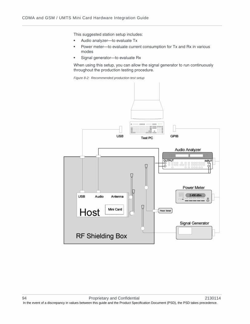
CDMA and GSM / UMTS Mini Card Hardware Integration Guide
This suggested station setup includes:
• Audio analyzer—to evaluate Tx
• Power meter—to evaluate current consumption for Tx and Rx in various modes
• Signal generator—to evaluate Rx
When using this setup, you can allow the signal generator to run continuously throughout the production testing procedure.
Figure 8-2: Recommended production test setup
94 Proprietary and Confidential 2130114 In the event of a discrepancy in values between this guide and the Product Specification Document (PSD), the PSD takes precedence.
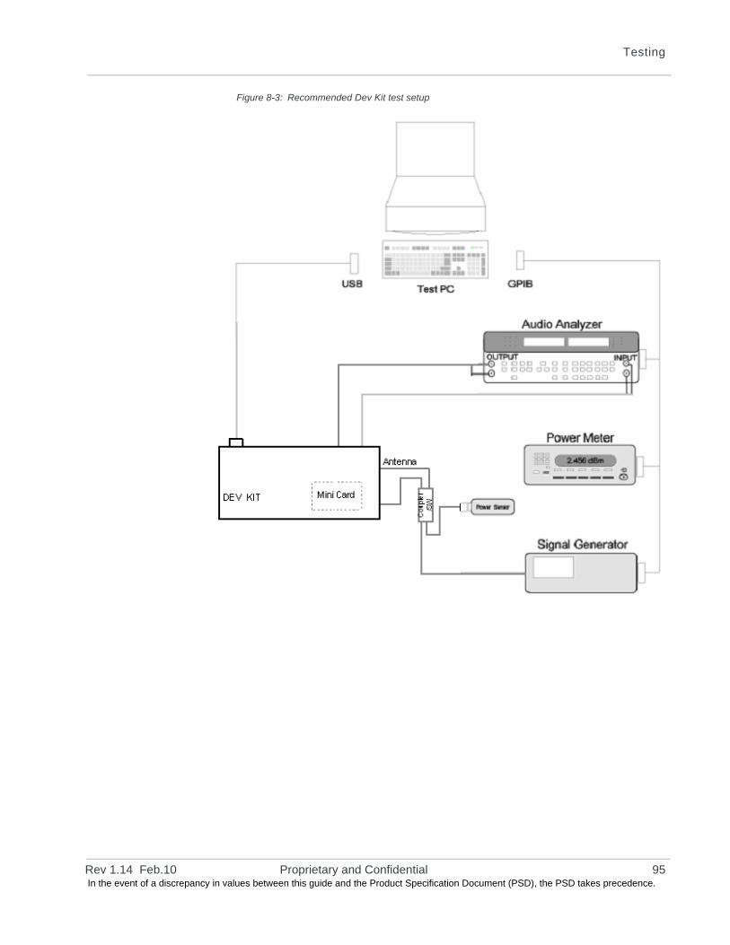
Testing
Figure 8-3: Recommended Dev Kit test setup
Rev 1.14 Feb.10 Proprietary and Confidential 95 In the event of a discrepancy in values between this guide and the Product Specification Document (PSD), the PSD takes precedence.

CDMA and GSM / UMTS Mini Card Hardware Integration Guide
96 Proprietary and Confidential 2130114 In the event of a discrepancy in values between this guide and the Product Specification Document (PSD), the PSD takes precedence.
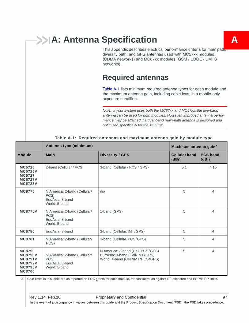
Rev 1.14 In the event
A
Module M
MC5725MC5725VMC5727MC5727VMC5728V
2
MC8775 NPEW
MC8775V NPEW
MC8780 E
MC8781 NP
MC8790MC8790VMC8791VMC8792VMC8795VMC8700
NPEW
a. Gain limits in th
AA: Antenna SpecificationThis appendix describes electrical performance criteria for main path, diversity path, and GPS antennas used with MC57xx modules (CDMA networks) and MC87xx modules (GSM / EDGE / UMTS networks).
Required antennas
Table A-1 lists minimum required antenna types for each module and the maximum antenna gain, including cable loss, in a mobile-only exposure condition.
Note: If your system uses both the MC87xx and MC57xx, the five-band antenna can be used for both modules. However, improved antenna perfor-mance may be attained if a dual-band main-path antenna is designed and optimized specifically for the MC57xx.
Table A-1: Required antennas and maximum antenna gain by module type
ntenna type (minimum) Maximum antenna gaina
ain Diversity / GPS Cellular band (dBi)
PCS band (dBi)
-band (Cellular / PCS) 3-band (Cellular / PCS / GPS) 5.1 4.15
.America: 2-band (Cellular/CS)ur/Asia: 3-bandorld: 5-band
n/a 5 4
.America: 2-band (Cellular/CS)ur/Asia: 3-bandorld: 5-band
1-band (GPS) 5 4
ur/Asia: 3-band 3-band (Cellular/IMT/GPS) 5 4
.America: 2-band (Cellular/CS)
3-band (Cellular/PCS/GPS) 5 4
.America: 2-band (Cellular/CS)ur/Asia: 3-bandorld: 5-band
N.America: 3-band (Cell/PCS/GPS)Eur/Asia: 3-band (Cell/IMT/GPS)World: 4-band (Cell/IMT/PCS/GPS)
5 4
is table are as reported on FCC grants for each module, for consideration against RF exposure and ERP/EIRP limits.
Feb.10 Proprietary and Confidential 97of a discrepancy in values between this guide and the Product Specification Document (PSD), the PSD takes precedence.
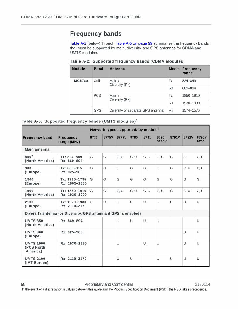
CDMA and GSM / UMTS Mini Card Hardware Integration Guide
Frequency bands
Table A-2 (below) through Table A-5 on page 99 summarize the frequency bands that must be supported by main, diversity, and GPS antennas for CDMA and UMTS modules.
Table A-2: Supported frequency bands (CDMA modules)
Module Band Antenna Mode Frequency range
MC57xx Cell Main /Diversity (Rx)
Tx 824–849
Rx 869–894
PCS Main /Diversity (Rx)
Tx 1850–1910
Rx 1930–1990
GPS Diversity or separate GPS antenna Rx 1574–1576
Table A-3: Supported frequency bands (UMTS modules)a
Network types supported, by moduleb
Frequency band Frequency range (MHz)
8775 8775V 8777V 8780 8781 87908790V
8791V 8792V 8795V8700
Main antenna
850c
(North America)Tx: 824–849Rx: 869–894
G G G, U G, U G, U G, U G G G, U
900(Europe)
Tx: 880–915Rx: 925–960
G G G G G G G G, U G, U
1800(Europe)
Tx: 1710–1785Rx: 1805–1880
G G G G G G G G G
1900(North America)
Tx: 1850–1910Rx: 1930–1990
G G G, U G, U G, U G, U G G, U G, U
2100(Europe)
Tx: 1920–1980Rx: 2110–2170
U U U U U U U U U
Diversity antenna (or Diversity / GPS antenna if GPS is enabled)
UMTS 850(North America)
Rx: 869–894 U U U U U
UMTS 900(Europe)
Rx: 925–960 U U
UMTS 1900(PCS North America)
Rx: 1930–1990 U U U U U
UMTS 2100(IMT Europe)
Rx: 2110–2170 U U U U U U
98 Proprietary and Confidential 2130114 In the event of a discrepancy in values between this guide and the Product Specification Document (PSD), the PSD takes precedence.
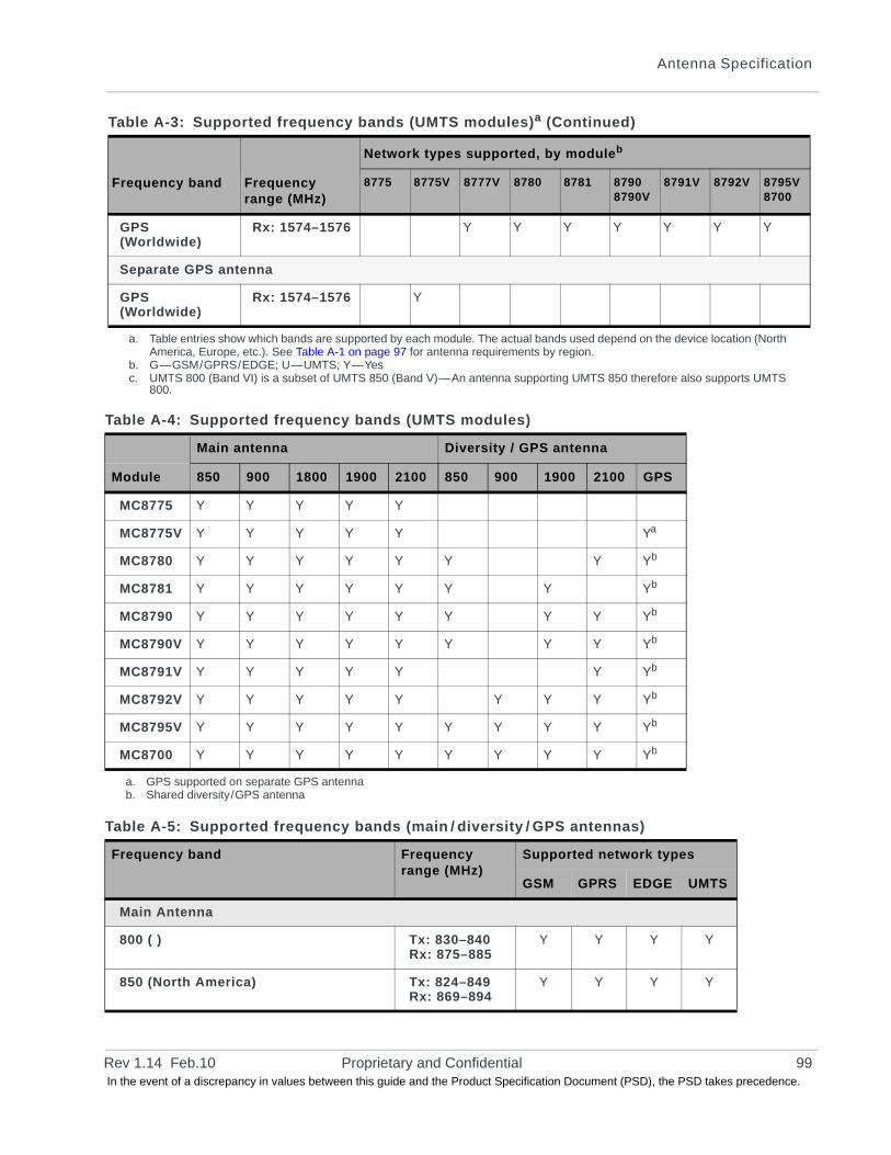
Antenna Specification
GPS(Worldwide)
Rx: 1574–1576 Y Y Y Y Y Y Y
Separate GPS antenna
GPS(Worldwide)
Rx: 1574–1576 Y
a. Table entries show which bands are supported by each module. The actual bands used depend on the device location (North America, Europe, etc.). See Table A-1 on page 97 for antenna requirements by region.
b. G—GSM/GPRS/EDGE; U—UMTS; Y—Yesc. UMTS 800 (Band VI) is a subset of UMTS 850 (Band V)—An antenna supporting UMTS 850 therefore also supports UMTS
800.
Table A-4: Supported frequency bands (UMTS modules)
Main antenna Diversity / GPS antenna
Module 850 900 1800 1900 2100 850 900 1900 2100 GPS
MC8775 Y Y Y Y Y
MC8775V Y Y Y Y Y Ya
MC8780 Y Y Y Y Y Y Y Yb
MC8781 Y Y Y Y Y Y Y Yb
MC8790 Y Y Y Y Y Y Y Y Yb
MC8790V Y Y Y Y Y Y Y Y Yb
MC8791V Y Y Y Y Y Y Yb
MC8792V Y Y Y Y Y Y Y Y Yb
MC8795V Y Y Y Y Y Y Y Y Y Yb
MC8700 Y Y Y Y Y Y Y Y Y Yb
a. GPS supported on separate GPS antennab. Shared diversity/GPS antenna
Table A-5: Supported frequency bands (main / diversity / GPS antennas)
Frequency band Frequency range (MHz)
Supported network types
GSM GPRS EDGE UMTS
Main Antenna
800 ( ) Tx: 830–840Rx: 875–885
Y Y Y Y
850 (North America) Tx: 824–849Rx: 869–894
Y Y Y Y
Table A-3: Supported frequency bands (UMTS modules)a (Continued)
Network types supported, by moduleb
Frequency band Frequency range (MHz)
8775 8775V 8777V 8780 8781 87908790V
8791V 8792V 8795V8700
Rev 1.14 Feb.10 Proprietary and Confidential 99 In the event of a discrepancy in values between this guide and the Product Specification Document (PSD), the PSD takes precedence.
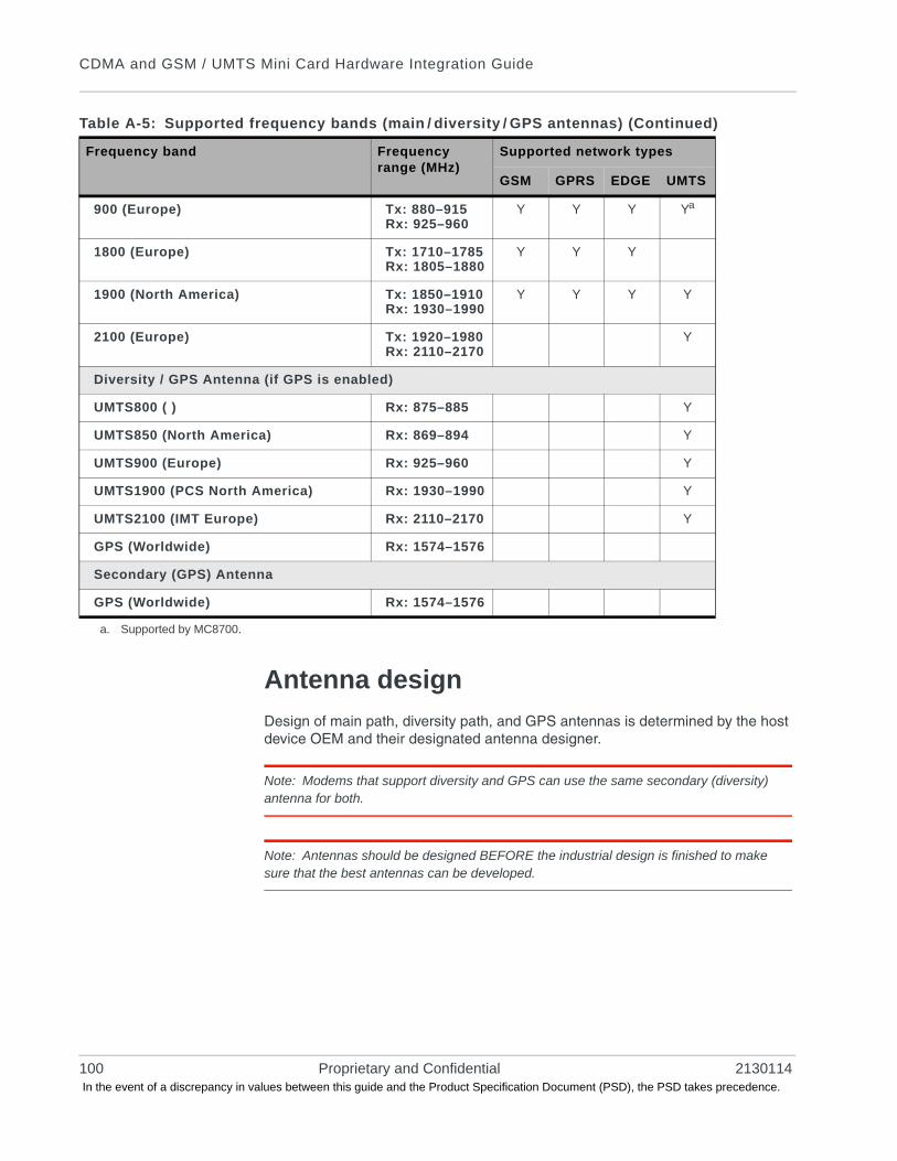
CDMA and GSM / UMTS Mini Card Hardware Integration Guide
Antenna design
Design of main path, diversity path, and GPS antennas is determined by the host device OEM and their designated antenna designer.
Note: Modems that support diversity and GPS can use the same secondary (diversity) antenna for both.
Note: Antennas should be designed BEFORE the industrial design is finished to make sure that the best antennas can be developed.
900 (Europe) Tx: 880–915Rx: 925–960
Y Y Y Ya
1800 (Europe) Tx: 1710–1785Rx: 1805–1880
Y Y Y
1900 (North America) Tx: 1850–1910Rx: 1930–1990
Y Y Y Y
2100 (Europe) Tx: 1920–1980Rx: 2110–2170
Y
Diversity / GPS Antenna (if GPS is enabled)
UMTS800 ( ) Rx: 875–885 Y
UMTS850 (North America) Rx: 869–894 Y
UMTS900 (Europe) Rx: 925–960 Y
UMTS1900 (PCS North America) Rx: 1930–1990 Y
UMTS2100 (IMT Europe) Rx: 2110–2170 Y
GPS (Worldwide) Rx: 1574–1576
Secondary (GPS) Antenna
GPS (Worldwide) Rx: 1574–1576
a. Supported by MC8700.
Table A-5: Supported frequency bands (main / diversity / GPS antennas) (Continued)
Frequency band Frequency range (MHz)
Supported network types
GSM GPRS EDGE UMTS
100 Proprietary and Confidential 2130114 In the event of a discrepancy in values between this guide and the Product Specification Document (PSD), the PSD takes precedence.
Antenna Specification
General antenna design requirements
In addition to passing the specific tests described in Testing beginning on page 102, the main path and diversity / GPS path antennas should satisfy the following requirements:
• Antenna impedance at feeding terminal = 50 (A simple matching circuit with six or fewer components is acceptable at the feeding terminal.)
• Nominally omni-directional radiation pattern in the azimuth plane
Main antenna design requirements
In addition to passing the specific tests described in Testing beginning on page 102, the main path antenna should satisfy the following requirements:
• Must handle 2 W RF power on low bands and 1 W on high bands
Measure the power using the following criteria:
• Measure power endurance over a period of 4 hours (estimated talk time) using a 2 W CW signal—set the frequency of the CW test signal to the middle of the PCS Tx band (1880 MHz for PCS).
• Visual inspection must prove there is no damage to the antenna structure and matching components.
• VSWR / TIS / TRP measurements taken before and after this test must show similar results.
Diversity antenna design requirements
(MC57xx/MC8780/MC8781/MC8790/MC8790V/MC8791V/MC8792V/MC8795V/MC8700)
Antenna diversity is required for end user performance and enhanced coverage on CDMA networks (800 MHz/1900 MHz) for MC57xx, and on UMTS networks (800 MHz/850 MHz/900 MHz/1900 MHz/2100 MHz) for MC8780/MC8781/MC8790/MC8790V/MC8791V/MC8792V/MC8795V/MC8700. (See Table A-4 on page 99 for UMTS diversity support by module.)
In addition to passing the specific tests described in Testing beginning on page 102, the diversity path antenna should satisfy the following requirement:
• Receive performance, measured by forward link throughput, must be 0 to 3 dB better than a single antenna
Performance goals
When designing the antenna system, consider the following performance goals:
• 0 dB gain antenna (or better)
• Diversity antenna receive performance to be similar to primary antenna
• Separation distance or polarity separation to achieve diversity antenna isolation of 10 db (minimum)—otherwise the receive antenna picks up too much power radiating from the primary antenna
Rev 1.14 Feb.10 Proprietary and Confidential 101 In the event of a discrepancy in values between this guide and the Product Specification Document (PSD), the PSD takes precedence.
CDMA and GSM / UMTS Mini Card Hardware Integration Guide
GPS antenna design requirements
(MC57xx/MC8775V/MC878x/MC879x)
A second antenna is required to access GPS functionality—if the modem also supports diversity, the same antenna can be used.
In addition to passing the specific tests described in Testing beginning on page 102, the diversity path antenna should satisfy the following requirements:
• Field of view (FOV): Omni-directional in azimuth, -45 to +90 in elevation
• Polarization (average Gv/Gh): > 0 dB. Vertical linear polarization is sufficient (no need to optimize for circular polarization)
• Free space average gain (Gv+Gh) over FOV: > -6 dBi (preferably > -3 dBi). Note: Average gain is the sum of average values (Gv + Gh) where both Gv and Gh are measured (and averaged) over -45 to +90 in elevation and ±180 in azimuth.
• Maximum gain and uniform coverage in the high elevation angle and zenith. Gain in the azimuth plane is not desired.
• Average 3D gain: > -5 dBi
• Typical VSWR: < 2:1
• Polarization: any other than LHCP (left-hand circular polarized) is acceptable
The same design procedures outlined in Interference and sensitivity on page 41 apply to the GPS path as well.
Testing
The performance specifications described in this section are valid while the antenna is mounted in the host device with the antenna feed cable routed in its final application configuration.
The following guidelines apply to the tests in this section:
• Perform electrical measurements at room temperature (+20°C to +26°C) unless otherwise specified
• For main and diversity path antennas, make sure the antennas (including contact device, coaxial cable, connectors, and matching circuit with no more than six components, if required) have nominal impedances of 50 across the frequency bands in Table A-5 on page 99.
• All tests (except isolation / correlation coefficient)—test the main or diversity antenna with the other antenna terminated.
• Any metallic part of the antenna system that is exposed to the outside environment needs to meet the electrostatic discharge tests per IEC61000-4-2 (conducted discharge +8kV).
• The functional requirements of the antenna system are tested and verified while the MiniCard antenna is integrated in the host device.
Note: Additional testing, including active performance tests, mechanical, and accelerated life tests can be discussed with Sierra Wireless’ engineering services. Contact your Sierra Wireless representative for assistance.
102 Proprietary and Confidential 2130114 In the event of a discrepancy in values between this guide and the Product Specification Document (PSD), the PSD takes precedence.
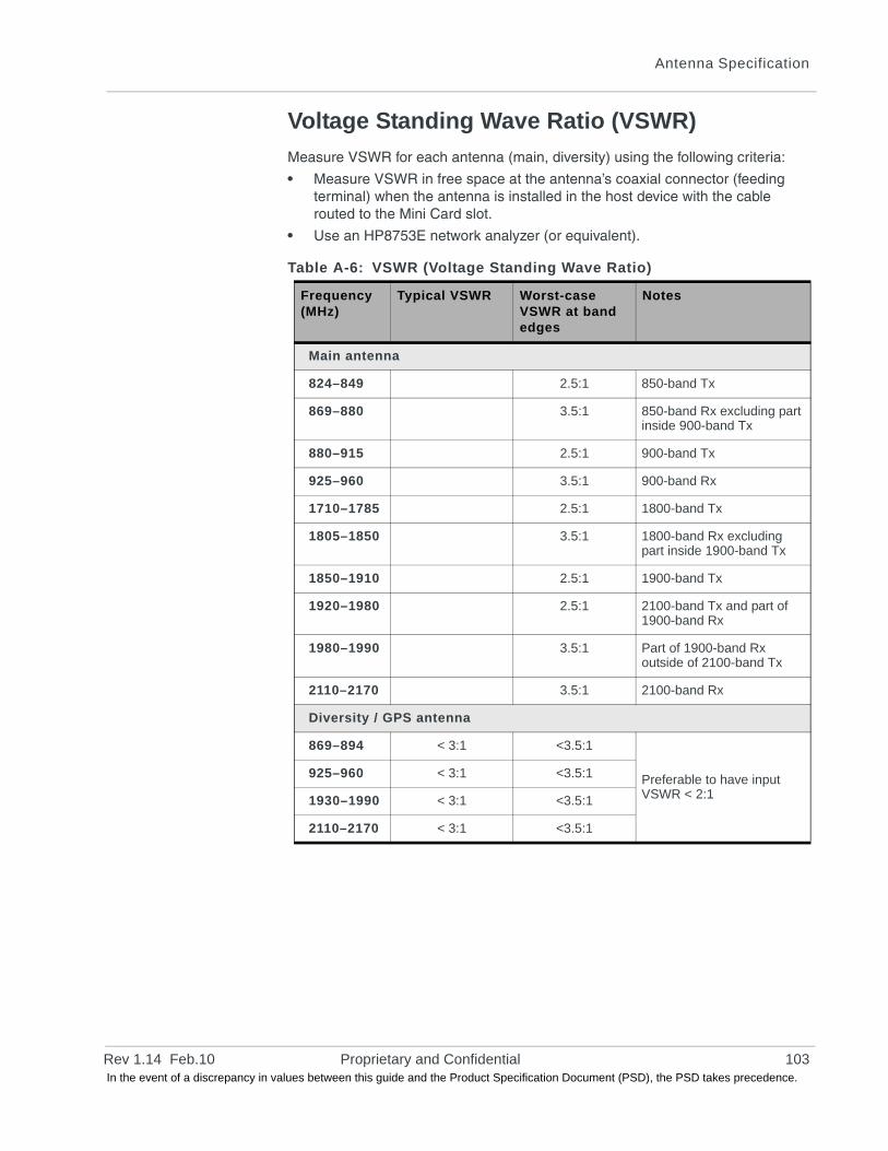
Antenna Specification
Voltage Standing Wave Ratio (VSWR)
Measure VSWR for each antenna (main, diversity) using the following criteria:
• Measure VSWR in free space at the antenna’s coaxial connector (feeding terminal) when the antenna is installed in the host device with the cable routed to the Mini Card slot.
• Use an HP8753E network analyzer (or equivalent).
Table A-6: VSWR (Voltage Standing Wave Ratio)
Frequency (MHz)
Typical VSWR Worst-case VSWR at band edges
Notes
Main antenna
824–849 2.5:1 850-band Tx
869–880 3.5:1 850-band Rx excluding part inside 900-band Tx
880–915 2.5:1 900-band Tx
925–960 3.5:1 900-band Rx
1710–1785 2.5:1 1800-band Tx
1805–1850 3.5:1 1800-band Rx excluding part inside 1900-band Tx
1850–1910 2.5:1 1900-band Tx
1920–1980 2.5:1 2100-band Tx and part of 1900-band Rx
1980–1990 3.5:1 Part of 1900-band Rx outside of 2100-band Tx
2110–2170 3.5:1 2100-band Rx
Diversity / GPS antenna
869–894 < 3:1 <3.5:1
Preferable to have input VSWR < 2:1
925–960 < 3:1 <3.5:1
1930–1990 < 3:1 <3.5:1
2110–2170 < 3:1 <3.5:1
Rev 1.14 Feb.10 Proprietary and Confidential 103 In the event of a discrepancy in values between this guide and the Product Specification Document (PSD), the PSD takes precedence.
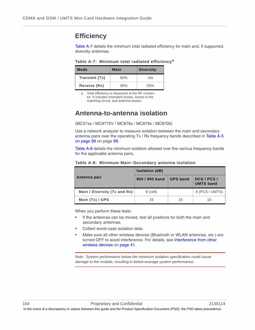
CDMA and GSM / UMTS Mini Card Hardware Integration Guide
Efficiency
Table A-7 details the minimum total radiated efficiency for main and, if supported, diversity antennas.
Antenna-to-antenna isolation
(MC57xx / MC8775V / MC878x / MC879x / MC8700)
Use a network analyzer to measure isolation between the main and secondary antenna pairs over the operating Tx / Rx frequency bands described in Table A-5 on page 99 on page 99.
Table A-8 details the minimum isolation allowed over the various frequency bands for the applicable antenna pairs.
When you perform these tests:
• If the antennas can be moved, test all positions for both the main and secondary antennas.
• Collect worst-case isolation data.
• Make sure all other wireless devices (Bluetooth or WLAN antennas, etc.) are turned OFF to avoid interference. For details, see Interference from other wireless devices on page 41.
Note: System performance below the minimum isolation specification could cause damage to the module, resulting in below-average system performance.
Table A-7: Minimum total radiated efficiencya
a. Total efficiency is measured at the RF connec-tor. It includes mismatch losses, losses in the matching circuit, and antenna losses.
Mode Main Diversity
Transmit (Tx) 50% n/a
Receive (Rx) 30% 25%
Table A-8: Minimum Main–Secondary antenna isolation
Antenna pair
Isolation (dB)
850 / 900 band GPS band DCS / PCS / UMTS band
Main / Diversity (Tx and Rx) 8 (cell) 8 (PCS / UMTS)
Main (Tx) / GPS 15 15 15
104 Proprietary and Confidential 2130114 In the event of a discrepancy in values between this guide and the Product Specification Document (PSD), the PSD takes precedence.
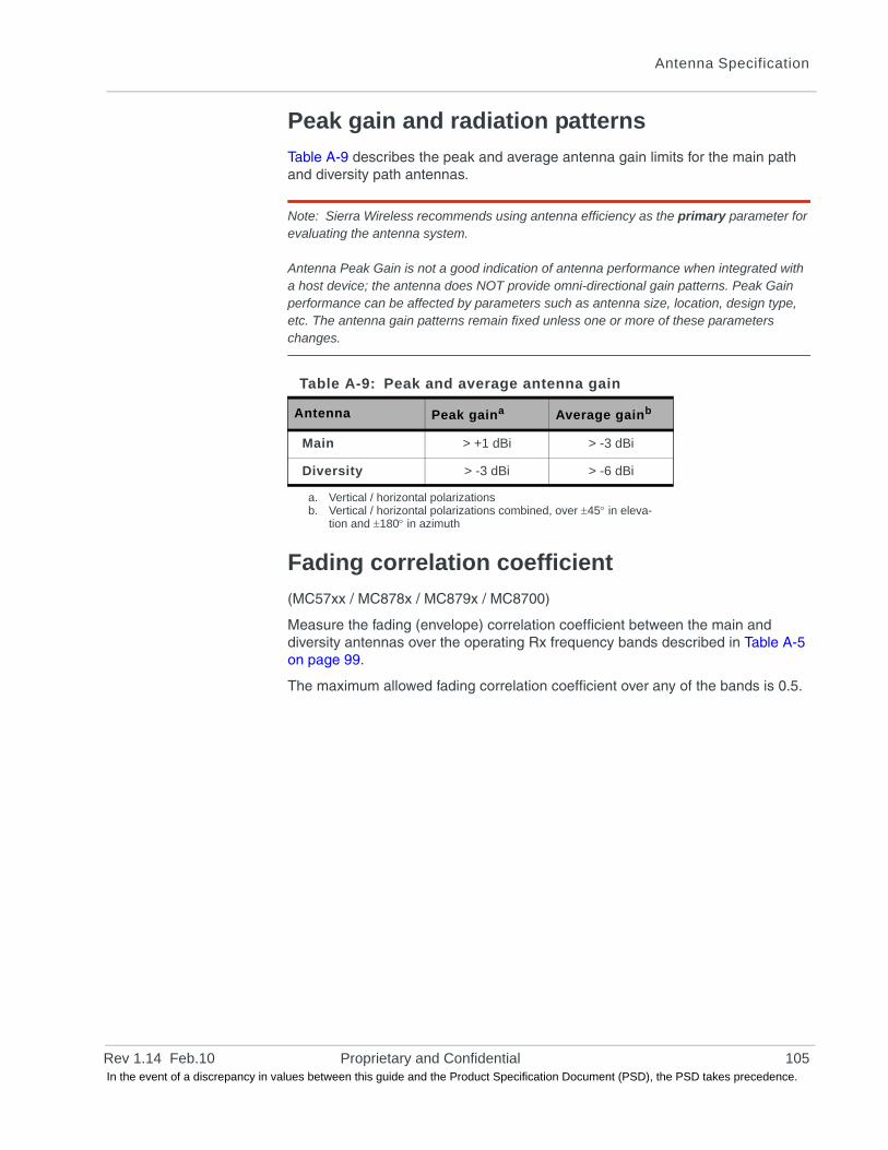
Antenna Specification
Peak gain and radiation patterns
Table A-9 describes the peak and average antenna gain limits for the main path and diversity path antennas.
Note: Sierra Wireless recommends using antenna efficiency as the primary parameter for evaluating the antenna system.
Antenna Peak Gain is not a good indication of antenna performance when integrated with a host device; the antenna does NOT provide omni-directional gain patterns. Peak Gain performance can be affected by parameters such as antenna size, location, design type, etc. The antenna gain patterns remain fixed unless one or more of these parameters changes.
Fading correlation coefficient
(MC57xx / MC878x / MC879x / MC8700)
Measure the fading (envelope) correlation coefficient between the main and diversity antennas over the operating Rx frequency bands described in Table A-5 on page 99.
The maximum allowed fading correlation coefficient over any of the bands is 0.5.
Table A-9: Peak and average antenna gain
Antenna Peak gaina
a. Vertical / horizontal polarizations
Average gainb
b. Vertical / horizontal polarizations combined, over 45 in eleva-tion and 180 in azimuth
Main > +1 dBi > -3 dBi
Diversity > -3 dBi > -6 dBi
Rev 1.14 Feb.10 Proprietary and Confidential 105 In the event of a discrepancy in values between this guide and the Product Specification Document (PSD), the PSD takes precedence.

CDMA and GSM / UMTS Mini Card Hardware Integration Guide
106 Proprietary and Confidential 2130114 In the event of a discrepancy in values between this guide and the Product Specification Document (PSD), the PSD takes precedence.
Rev 1.14 In the event
BB: Regulatory Information
Important notice
Because of the nature of wireless communications, transmission and reception of data can never be guaranteed. Data may be delayed, corrupted (i.e., have errors) or be totally lost. Although significant delays or losses of data are rare when wireless devices such as the Sierra Wireless modem are used in a normal manner with a well-constructed network, the Sierra Wireless modem should not be used in situations where failure to transmit or receive data could result in damage of any kind to the user or any other party, including but not limited to personal injury, death, or loss of property. Sierra Wireless and its affiliates accept no responsibility for damages of any kind resulting from delays or errors in data transmitted or received using the Sierra Wireless modem, or for failure of the Sierra Wireless modem to transmit or receive such data.
Safety and hazards
Do not operate your MC57xx / MC87xx modem:
• In areas where blasting is in progress
• Where explosive atmospheres may be present including refuelling points, fuel depots, and chemical plants
• Near medical equipment, life support equipment, or any equipment which may be susceptible to any form of radio inter-ference. In such areas, the MC57xx / MC87xx modem MUST BE POWERED OFF. Otherwise, the MC57xx / MC87xx modem can transmit signals that could interfere with this equipment.
In an aircraft, the MC57xx / MC87xx modem MUST BE POWERED OFF. Otherwise, the MC57xx / MC87xx modem can transmit signals that could interfere with various onboard systems and may be dangerous to the operation of the aircraft or disrupt the cellular network. Use of a cellular phone in an aircraft is illegal in some jurisdictions. Failure to observe this instruction may lead to suspension or denial of cellular telephone services to the offender, or legal action or both.
Some airlines may permit the use of cellular phones while the aircraft is on the ground and the door is open. The MC57xx / MC87xx modem may be used normally at this time.
Feb.10 Proprietary and Confidential 107of a discrepancy in values between this guide and the Product Specification Document (PSD), the PSD takes precedence.
CDMA and GSM / UMTS Mini Card Hardware Integration Guide
Important compliance information for North American users
The MC57xx / MC87xx modem has been granted modular approval for mobile applications. Integrators may use the MC57xx / MC87xx modem in their final products without additional FCC / IC (Industry Canada) certification if they meet the following conditions. Otherwise, additional FCC / IC approvals must be obtained.
1. At least 20 cm separation distance between the antenna and the user’s body must be maintained at all times.
2. To comply with FCC / IC regulations limiting both maximum RF output power and human exposure to RF radiation, the maximum antenna gain including cable loss in a mobile-only exposure condition must not exceed the levels detailed in Table A-1, Required antennas and maximum antenna gain by module type, on page 97.
3. The MC57xx / MC87xx modem and its antenna must not be co-located or operating in conjunction with any other transmitter or antenna within a host device.
4. A label must be affixed to the outside of the end product into which the MC57xx / MC87xx modem is incorporated, with a statement similar to the following:· For MC5725 / MC5725V:
This device contains FCC ID: N7N-MC5725This equipment contains equipment certified under IC: 2417C-MC5725
· For MC5727 / MC5727V:This device contains FCC ID: N7N-MC5727This equipment contains equipment certified under IC: 2417C-MC5727
· For MC5728V:This device contains FCC ID: N7N-MC5728This equipment contains equipment certified under IC: 2417C-MC5728
· For MC8775 / MC8775V: This device contains FCC ID: N7NMC8775This equipment contains equipment certified under IC: 2417C-MC8775
· For MC8780: This device contains FCC ID: N7NMC8780
· For MC8781: This device contains FCC ID: N7NMC8781This equipment contains equipment certified under IC: 2417C-MC8781
· For MC8790 / MC8790V: This device contains FCC ID: N7NMC8790This equipment contains equipment certified under IC: 2417C-MC8790
· For MC8792V: This device contains FCC ID: N7NMC8792This equipment contains equipment certified under IC: 2417C-MC8792
· For MC8795V: This device contains FCC ID: N7NMC8795This equipment contains equipment certified under IC: 2417C-MC8795
108 Proprietary and Confidential 2130114 In the event of a discrepancy in values between this guide and the Product Specification Document (PSD), the PSD takes precedence.
Regulatory Information
· For MC8700: This device contains FCC ID: N7NMC8700This equipment contains equipment certified under IC: 2417C-MC8700
5. A user manual with the end product must clearly indicate the operating requirements and conditions that must be observed to ensure compliance with current FCC / IC RF exposure guidelines.
The end product with an embedded MC57xx / MC87xx modem may also need to pass the FCC Part 15 unintentional emission testing requirements and be properly authorized per FCC Part 15.
Note: If this module is intended for use in a portable device, you are responsible for separate approval to satisfy the SAR requirements of FCC Part 2.1093 and IC RSS-102.
EU regulatory conformity
Sierra Wireless hereby declares that the MC8775, MC8775V, MC8780, MC8790, MC8790V, MC8791V, MC8792V, MC8795V, and MC8700 modems conform with all essential requirements of Directive 1999/5/EC.
MC8775, MC8775V, MC8780, MC8790, MC8790V, MC8791V, MC8792V:
MC8795V:
MC8700:
The Declaration of Conformity made under Directive 1999/5/EC is available for viewing at the following location in the EU community:
Sierra Wireless (UK), LimitedLakeside House1 Furzeground Way, Stockley Park EastUxbridge, MiddlesexUB11 1BDEngland
Rev 1.14 Feb.10 Proprietary and Confidential 109 In the event of a discrepancy in values between this guide and the Product Specification Document (PSD), the PSD takes precedence.
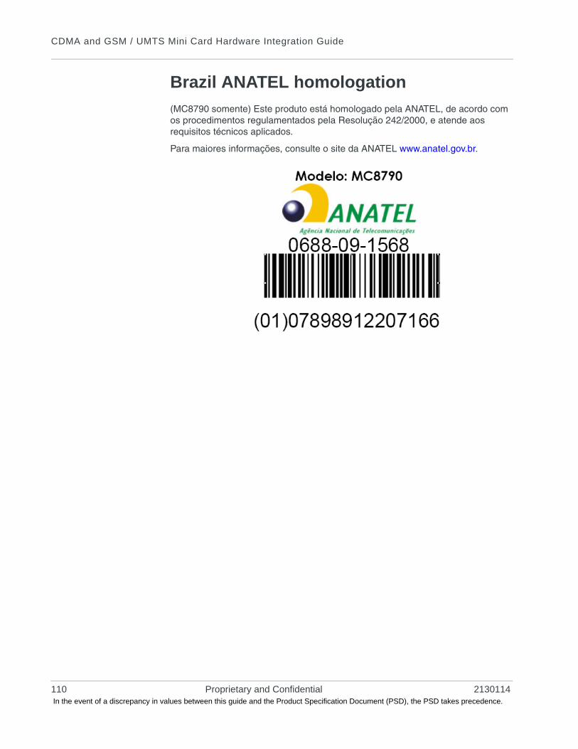
CDMA and GSM / UMTS Mini Card Hardware Integration Guide
Brazil ANATEL homologation
(MC8790 somente) Este produto está homologado pela ANATEL, de acordo com os procedimentos regulamentados pela Resolução 242/2000, e atende aos requisitos técnicos aplicados.
Para maiores informações, consulte o site da ANATEL www.anatel.gov.br.
110 Proprietary and Confidential 2130114 In the event of a discrepancy in values between this guide and the Product Specification Document (PSD), the PSD takes precedence.
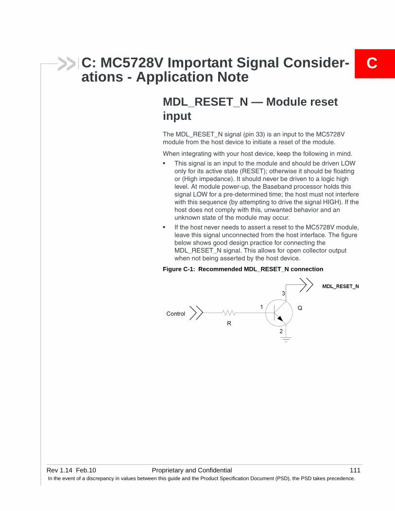
Rev 1.14 In the event
CC: MC5728V Important Signal Consider-ations - Application Note
MDL_RESET_N — Module reset input
The MDL_RESET_N signal (pin 33) is an input to the MC5728V module from the host device to initiate a reset of the module.
When integrating with your host device, keep the following in mind.
• This signal is an input to the module and should be driven LOW only for its active state (RESET); otherwise it should be floating or (High impedance). It should never be driven to a logic high level. At module power-up, the Baseband processor holds this signal LOW for a pre-determined time; the host must not interfere with this sequence (by attempting to drive the signal HIGH). If the host does not comply with this, unwanted behavior and an unknown state of the module may occur.
• If the host never needs to assert a reset to the MC5728V module, leave this signal unconnected from the host interface. The figure below shows good design practice for connecting the MDL_RESET_N signal. This allows for open collector output when not being asserted by the host device.
Figure C-1: Recommended MDL_RESET_N connection
Feb.10 Proprietary and Confidential 111of a discrepancy in values between this guide and the Product Specification Document (PSD), the PSD takes precedence.
CDMA and GSM / UMTS Mini Card Hardware Integration Guide
W_Disable# — Wireless disable
The W_Disable# signal (pin 20) is an input to the module from the host device to control the Power state (power on and shutdown of the MC5728V module, depending on the state of the signal).
When integrating with your host device, keep the following in mind.
• This signal is an input to the module and should be driven LOW only for its active state (controlling the power state); otherwise it should be floating or (High impedance). It should never be driven to a logic high level. The MC5728V module has an internal pull-up resistor to Module Power (3.3V) in place, so if the signal is floating or (high impedance), the module will power on.
• If the host never needs to assert this power state control to the MC5728V module, leave this signal unconnected from the host interface. Figure 2-1 on page 17 shows good design practice for connecting the W_DISABLE# signal. This allows for open collector output when not being asserted by the host device.
112 Proprietary and Confidential 2130114 In the event of a discrepancy in values between this guide and the Product Specification Document (PSD), the PSD takes precedence.
Rev 1.14 In the event
DD: Acronyms and Definitions.
Table D-1: Acronyms and definitions
Acronym or term Definition
AGC Automatic Gain Control
BER Bit Error Rate - a measure of receive sensitivity
BLER Block Error Rate
Call Box Base Station Simulator - Agilent E8285A or 8960, Rohde & Schwarz CMU200
CDMA Code Division Multiple Access
dB Decibel = 10 x log10 (P1/P2)P1 is calculated power; P2 is reference power
Decibel = 20 x log10 (V1/V2)V1 is calculated voltage, V2 is reference voltage
dBm Decibels, relative to 1 mW - Decibel(mW) = 10 x log10 (Pwr (mW)/1mW)
DUT Device Under Test
EDGE Enhanced Data rates for GSM Evolution
EM Embedded Module
ESD ElectroStatic Discharge
FER Frame Error Rate - a measure of receive sensitivity
GPRS General Packet Radio Services
GPS Global Positioning System
GSM Global System for Mobile communications
Hz Hertz = 1 cycle/second
inrush current Peak current drawn when a device is connected or powered on
IS-2000 3G radio standards for voice and data (CDMA only)
IS-95 2G radio standards targeted for voice (cdmaONE)
LDO Low Drop Out - refers to linear regulator
MC5725 / MC5725V / MC5727 / MC5727V / MC5728V
Sierra Wireless Mini Cards used on CDMA networks
MC57xx Any of the following CDMA Mini Cards: MC5725 / MC5725V / MC5727 / MC5727V / MC5728V
Feb.10 Proprietary and Confidential 113of a discrepancy in values between this guide and the Product Specification Document (PSD), the PSD takes precedence.
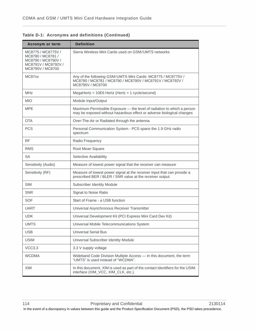
CDMA and GSM / UMTS Mini Card Hardware Integration Guide
MC8775 / MC8775V /MC8780 / MC8781 / MC8790 / MC8790V / MC8791V / MC8792V / MC8795V / MC8700
Sierra Wireless Mini Cards used on GSM/UMTS networks
MC87xx Any of the following GSM/UMTS Mini Cards: MC8775 / MC8775V / MC8780 / MC8781 / MC8790 / MC8790V / MC8791V / MC8792V / MC8795V / MC8700
MHz MegaHertz = 10E6 Hertz (Hertz = 1 cycle/second)
MIO Module Input/Output
MPE Maximum Permissible Exposure — the level of radiation to which a person may be exposed without hazardous effect or adverse biological changes
OTA Over-The-Air or Radiated through the antenna
PCS Personal Communication System - PCS spans the 1.9 GHz radio spectrum
RF Radio Frequency
RMS Root Mean Square
SA Selective Availability
Sensitivity (Audio) Measure of lowest power signal that the receiver can measure
Sensitivity (RF) Measure of lowest power signal at the receiver input that can provide a prescribed BER / BLER / SNR value at the receiver output.
SIM Subscriber Identity Module
SNR Signal to Noise Ratio
SOF Start of Frame - a USB function
UART Universal Asynchronous Receiver Transmitter
UDK Universal Development Kit (PCI Express Mini Card Dev Kit)
UMTS Universal Mobile Telecommunications System
USB Universal Serial Bus
USIM Universal Subscriber Identity Module
VCC3.3 3.3 V supply voltage
WCDMA Wideband Code Division Multiple Access — In this document, the term “UMTS” is used instead of “WCDMA”.
XIM In this document, XIM is used as part of the contact identifiers for the USIM interface (XIM_VCC, XIM_CLK, etc.).
Table D-1: Acronyms and definitions (Continued)
Acronym or term Definition
114 Proprietary and Confidential 2130114 In the event of a discrepancy in values between this guide and the Product Specification Document (PSD), the PSD takes precedence.
Rev 1. In the e
Index
Numerics
1XCDMA Standard 13
A
acceptance tests 75acronyms and definitions 113–114airplane mode 19anechoic chamber, OTA testing 43antenna
connection and mounting points 39connection considerations 39custom, considerations 40design requirements, diversity antenna 101design requirements, general 101design requirements, GPS 102design requirements, main antenna 101diversity antenna, disabling 41diversity, MC57xx 101diversity, MC87xx 101frequency bands, supported 98GPS, MC57xx / MC8775V / MC878x / MC879x /
MC8700 102limit, matching coaxial connections 39location, considerations 41matching, considerations 40maximum cable loss 39specification 97–105testing 102
antennasdesign checklist 73frequency bands supported, by antenna type 99frequency bands supported, MC57xx 98frequency bands supported, MC87xx 99required, by module type and gain 97
AT commands3GPP specification, details 13extended, MC57xx 67extended, MC87xx 68extended, overview 67low power mode, setting 19standard, MC57xx (reference document) 13standard, MC87xx (reference document) 14
AT commands, extendedMC57xx, reference 13MC87xx, reference 14
AT commands, standardMC57xx, reference 13MC87xx, reference 14
audiofeatures, summary 51functions, host-controlled 58functions, module-controlled 58functions, responsible codecs 52interface 51–58
path mixing, host-controlled 58path switching, host-controlled 58PCM digital, signal interface 58primary, signal interface 57signal interface 57system block diagram, MC5725V 52system block diagram, MC5727V 52system block diagram, MC5728V 53system block diagram, MC87xxV 54
audio modes, supported 55audio pass band 51audio passband, Rx and Tx 57automatic gain control (AGC)
module-controlled 58
B
BER (Bit Error Rate) 45bit error rate (BER)
measure of sensitivity, MC87xx 45
C
cable lossantenna, maximum 39
capacitanceinrush current, effect on 25
capacitorswith USIM 66with XIM_DATA / XIM_CLK 66
car kit audio mode 51car kit mode
echo cancellation 57CDMA
1X Standard 13cellular band
RF parameters, MC57xx 37certification tests 76checklist, design 73CnS
MC57xx reference 13MC87xx reference 14notification issued, state change
temperature 23voltage 20, 21
voice reference 14codec
for audio functions 52comfort noise
module-controlled 58communications, host to modem
design checklist 74connection
grounding 40connectors, required
EDGE mating (52-pin) 12
14 Feb.10 Proprietary and Confidential 115vent of a discrepancy in values between this guide and the Product Specification Document (PSD), the PSD takes precedence.
CDMA and GSM / UMTS Mini Card Hardware Integration Guide
host-module 12RF, Hirose 12USIM 12
currentconsumption 27–36consumption, usage models 36peak inrush current, calculation 25specifications, MC57xx 28specifications, MC8700 33–34specifications, MC8775/75V 28–30specifications, MC8780/81 30–31specifications, MC8790/90V/91V/92V/95V 31–32, 32–33
current, consumption 27
D
DCS 1800RF parameters, MC87xx 37sensitivity, test results 48
desense. See RFdesign checklist
antennas 73component placement 73EMI/ESD 74host/modem communications 74power 73thermal 74
devicepositioning, sensitivity testing 44
disconnected, module power state 19diversity antenna
disabling 41DTMF
codec 52module-controlled 58
E
echo cancellationaudio feature 51codec 52details 56module-controlled 58support, all modes 56
EDGE connector, manufacturers 12efficiency
test criteria 104EGSM 900
RF parameters, MC87xx 37sensitivity, test results 47
electrostatic discharge. See ESDESD
design checklist 74protection requirements 18testing techniques document (IEC-61000-4-2) 13
F
fading correlation coefficienttest criteria 105
FCCregulations, relevant section 13
FER (Frame Error Rate) 45filtering
high pass / slope filtering, module-controlled 58filtering stages, audio 51filtering, RF desense 42FIR filtering
audio feature 51codec 52module-controlled 58
frame error rate (FER)measure of sensitivity, MC57xx 45
frequency bands, supported 98
G
gaincodec 52distribution, audio 56limits, adjustable 51
gain, antennatest criteria 105
GPS bandRF parameters, MC57xx 37RF parameters, MC87xx 38
GPS sensitivityconducted, RF parameter, MC87xx 37
groundingconnection considerations 40
GSM 1900sensitivity, test results 48
GSM 850RF parameters, MC87xx 37sensitivity, test results 47
H
handset audio mode 51handset mode
echo cancellation 56handshaking
USB 61headset audio mode 51headset mode
echo cancellation 56Host•Module interface 59–70
I
I/O rise time requirements 66impedance
module-antenna 41USIM 66
116 Proprietary and Confidential 2130114 In the event of a discrepancy in values between this guide and the Product Specification Document (PSD), the PSD takes precedence.
Index
inrush currentsdescription 24host power supply applied 25model, MC57xx 24model, MC87xx 25W_Disable# deasserted 25
interfaceaudio signal 57
interferencedevice generated 42power supply noise 41wireless devices 41
isolationtest criteria 104
L
LEDexample 63states 62
low power modesetting, AT commands 19state change from normal, temperature 23state change from normal, voltage 20state change to normal, temperature 23state change to normal, voltage 21temperature trigger levels 22voltage trigger levels 20
low power, module power state 19
M
MC5725AT commands, extended 67AT reference (extended) 13AT reference (standard) 13CnS reference 13networks supported 11product specification 13RF parameters (MC57xx) 37
MC5725VAT commands, extended 67AT reference (extended) 13AT reference (standard) 13audio interface, supported 51CnS reference 13networks supported 11product specification 13RF parameters (MC57xx) 37
MC5727AT commands, extended 67AT reference (extended) 13AT reference (standard) 13CnS reference 13networks supported 11product specification 13RF parameters (MC57xx) 37
MC5727V
AT commands, extended 67AT reference (extended) 13AT reference (standard) 13audio interface, supported 51CnS reference 13networks supported 11product specification 14RF parameters (MC57xx) 37
MC5728VAT commands, extended 67AT reference (extended) 13AT reference (standard) 13audio interface, supported 51CnS reference 13important signal considerations 111networks supported 11product specification 14RF parameters (MC57xx) 37
MC57xxcurrent specifications 28sensitivity test results 46sensitivity, defined 45
MC8700AT reference (extended), and MC87xx 14AT reference (standard), and MC87xx 14CnS reference, and MC87xx 14current specifications 33–34networks supported 11power consumption 34product specification 14RF parameters 37
MC8775AT reference (extended), and MC87xx 14AT reference (standard), and MC87xx 14CnS reference, and MC87xx 14current specifications 28–30networks supported 11product specification 14RF parameters 37
MC8775VAT reference (extended), and MC87xx 14AT reference (standard), and MC87xx 14audio interface, supported 51CnS reference, and MC87xx 14CnS voice reference, and MC87xxV 14current specifications 28–30networks supported 11product specification 14RF parameters 37
MC8780AT reference (extended), and MC87xx 14AT reference (standard), and MC87xx 14CnS reference, and MC87xx 14current specifications 30–31networks supported 11power consumption 34product specification 14RF parameters 37
MC8781
Rev 1.14 Feb.10 Proprietary and Confidential 117 In the event of a discrepancy in values between this guide and the Product Specification Document (PSD), the PSD takes precedence.
CDMA and GSM / UMTS Mini Card Hardware Integration Guide
AT reference (extended), and MC87xx 14AT reference (standard), and MC87xx 14CnS reference, and MC87xx 14current specifications 30–31networks supported 11power consumption 34product specification 14RF parameters 37
MC8790AT reference (extended), and MC87xx 14AT reference (standard), and MC87xx 14CnS reference, and MC87xx 14current specifications 31–32, 32–33networks supported 11power consumption 34product specification 14RF parameters 37
MC8790VAT reference (extended), and MC87xx 14AT reference (standard), and MC87xx 14audio interface, supported 51CnS reference, and MC87xx 14CnS voice reference, and MC87xxV 14current specifications 31–32, 32–33networks supported 11power consumption 34product specification 14RF parameters 37
MC8791VAT reference (extended), and MC87xx 14AT reference (standard), and MC87xx 14audio interface, supported 51CnS reference, and MC87xx 14CnS voice reference, and MC87xxV 14current specifications 31–32, 32–33networks supported 11power consumption 34product specification 14RF parameters 37
MC8792VAT reference (extended), and MC87xx 14AT reference (standard), and MC87xx 14audio interface, supported 51CnS reference, and MC87xx 14CnS voice reference, and MC87xxV 14current specifications 31–32, 32–33networks supported 11power consumption 34product specification 14RF parameters 37
MC8795VAT reference (extended), and MC87xx 14AT reference (standard), and MC87xx 14audio interface, supported 51CnS reference, and MC87xx 14CnS voice reference, and MC87xxV 14current specifications 31–32, 32–33networks supported 11power consumption 34
product specification 14RF parameters 37
MC87xxAT commands, extended 68sensitivity test results 47–50sensitivity, defined 45
MC87xxVpins, connector (2.6V) 59, 60
MDL_RESET_N (MC5728V) 111Mini Card
Dev Kit Quick Start Guide 15PCI Express Specification 15See also MC5725, MC5725V, MC5727, MC5727V,
MC5728V, MC8775, MC8775V, MC8780,MC8781, MC8790, MC8790V, MC8791V,MC8792V, MC8795V, MC8700
minicomdownloading and installing 82
mixingcodec 52
modesdeep sleep, description 35operating 35shutdown, description 35sleep, description 35transmit / receive, description 35
modulepower states 18–24
N
networkssupported, by module type 11
noiseleakage, minimizing 40RF interference, power supply 41
noise suppressionaudio feature 51module-controlled 58
normal modestate change from low power, temperature 23state change from low power, voltage 21state change to low power, temperature 23state change to low power, voltage 20
normal, module power state 19
O
off, module power state 19output driver stage, audio feature 51
P
path loss, OTA testing 44path switching
codec 52PCB
multi-layer, shielding for RF desense 42
118 Proprietary and Confidential 2130114 In the event of a discrepancy in values between this guide and the Product Specification Document (PSD), the PSD takes precedence.
Index
PCI ExpressMini Card specification 15
PCM digital audio, signal interface 58PCS 1900
RF parameters, MC87xx 37PCS band
RF parameters, MC57xx 37pins
connector (2.6V), MC87xxV 59, 60polyphonic ringtone
host-controlled 58power
consumption, MC8780/81/90/90V/91V/92V/95V/00 34current consumption, overview 27default state 19design checklist 73disconnected, characteristics 19normal, characteristics 19off, characteristics 19off, state change, temperature 23off, state change, voltage 21power-up timing 26ramp-up timing 26required supply voltage 17signals, overview 17state machine, temperature monitoring 22–24state machine, voltage monitoring 20–21state, disconnected 19state, low power 19state, normal 19state, off 19states, module 18–24supply, RF interference 41supply, ripple limit 41transmit, wave form 26
power interface 17–36product specification (PSD) 13, 14production tests 77PSD (Product Specification Document) 13, 14
Q
quality assurance tests 93
R
regulatory information 107–110Brazil 110EU 109FCC 108limitation of liability 107safety and hazards 107
reset module, input (MC5728V) 111resistors, external pull-up 66resume
mode, USB 62RF
antenna cable loss, maximum 39
antenna connection, considerations 39cable type, required 12desense
device-generated 42harmonic energy, filtering 42mitigation suggestions 42shielding suggestions 42
integration 37–50interference
other devices 42power supply 41wireless devices 41
level lowered automatically, high temperature 24parameters
cellular band, MC57xx 37GPS, MC57xx 37MC57xx 37MC87xx 37PCS band, MC57xx 37
parameters, MC87xxDCS 1800 37EGSM 900 37GPS 38GSM 850 37PCS 1900 37UMTS 1900 38UMTS 2100 38UMTS 850 38
ringer tonecodec 52
ringersmodule-controlled 58
ringtone, polyphonichost-controlled 58
Rx bandRF parameters, MC57xx 37
Rx sensitivityconducted, RF parameter, MC87xx 37RF parameter, MC57xx 37
S
SCI (Slot Cycle Index) 28SED
see Smart Error Detectionsensitivity
conducted, RF parameter, MC87xx 37defined, MC57xx and MC87xx 45GPS conducted, MC87xx 37MC57xx, defined (frame error rate) 45MC87xx, defined (bit error rate) 45measurements 47–50radiated measurement, overview 43RF parameter, MC57xx 37test results
MC57xx 46MC87xx 47–50
testingdevice under test, positioning 44
Rev 1.14 Feb.10 Proprietary and Confidential 119 In the event of a discrepancy in values between this guide and the Product Specification Document (PSD), the PSD takes precedence.
CDMA and GSM / UMTS Mini Card Hardware Integration Guide
testing, overview 43testing, path loss calculation 44
sensitivity, OTA test chamber configuration 43shielding
module, compliance 40reducing RF desense 42
sidetoneresponsible codec 58support 55
SIMtesting methods, MS conformance specification 15See also USIM
Slot Cycle Index 28Smart Error Detection
detecting module reset 35speakerphone audio mode 51speakerphone mode
echo cancellation 57state machine
temperature monitoring 22–24voltage monitoring 20–21
suspendmode, USB 61
system blockMC5725V, audio 52MC5727V, audio 52MC5728V, audio 53MC87xxV, audio 54
T
temperature monitoring state machinetrigger levels 22
temperature, module. See thermaltest
efficiency 104fading correlation coefficient 105gain, antenna 105isolation 104VSWR (Voltage Standing Wave Ratio) 103
testingoverview 75acceptance tests 75audio loop-back, MC5725V / MC5727V / MC5728V /
MC8775V / MC8790V / MC8791V / MC8792V 91certification tests 76equipment, suggested 93ESD immunity, techniques document (IEC-61000-4-2) 13GPS receiver, MC8775V 90manual functional test, suggested 77production tests 77quality assurance tests 93RF receive path, MC57xx 86RF receive path, MC87xx 87RF transmission path, MC57xx 82RF transmission path, MC87xx 84sensitivity, OTA test chamber configuration 43suggestions 75–95
testing, path loss calculation 45
thermalconsiderations 71–72design checklist 74dissipation, factors affecting 71dissipation, suggestions 71RF shield temperature, maximum 72testing, module 71–72
timingpower ramp-up 26power-up 26
transducer interfacehost-controlled 58
transducer interfacescodec 52
transmit power wave form 26Tx band
RF parameters, MC57xx 37Tx power
conducted, RF parameter, MC87xx 37RF parameters, MC57xx 37
U
UDK (Universal Development Kit)components, included 11
UMTS 1900RF parameters, MC87xx 38sensitivity, test results 50
UMTS 2100RF parameters, MC87xx 38sensitivity, test results 50
UMTS 850RF parameters, MC87xx 38sensitivity, test results 49
Universal Development Kit (UDK)components, included 11
Universal Serial Bus. See USB.usage models
current consumption 36USB
enumeration, power-up 26handshaking 61host driver requirements 62interface
host•module communication 61–62overview 61
resume mode 62specification 15suspend mode 61
USIMcapacitor recommendations 66card contacts 65clock rate 66connector type, required 12electrical specifications 66impedance, connectors 66interface diagram 65interface, overview 64operation 66–67
120 Proprietary and Confidential 2130114 In the event of a discrepancy in values between this guide and the Product Specification Document (PSD), the PSD takes precedence.
Index
pin assignments 64socket placement 66
V
voice memohost-controlled 58
voltage monitoring state machinetrigger levels 20
Voltage Standing Wave Ratio (VSWR)test criteria 103
volume, settingresponsible codec 58
VSWR (Voltage Standing Wave Ratio)test criteria 103
W
W_Disable#deasserted, causes inrush current event 25de-asserted, peak current 25inrush currents 24MC5728V information 112module, powering off 21, 23Normal state 19off state 19
Z
ZIF (Zero Intermediate Frequency) 41
Rev 1.14 Feb.10 Proprietary and Confidential 121 In the event of a discrepancy in values between this guide and the Product Specification Document (PSD), the PSD takes precedence.
CDMA and GSM / UMTS Mini Card Hardware Integration Guide
122 Proprietary and Confidential 2130114 In the event of a discrepancy in values between this guide and the Product Specification Document (PSD), the PSD takes precedence.