cell proliferation tracking using graphene sensor - school of physics
TRANSCRIPT
Hindawi Publishing CorporationJournal of SensorsVolume 2012, Article ID 219485, 7 pagesdoi:10.1155/2012/219485
Research Article
Cell Proliferation Tracking Using Graphene Sensor Arrays
Ronan Daly,1 Shishir Kumar,1 Gyongyi Lukacs,2 Kangho Lee,1 Anne Weidlich,1
Martin Hegner,2 and Georg S. Duesberg1
1 CRANN and School of Chemistry, Trinity College Dublin, Dublin 2, Ireland2 CRANN and School of Physics, Trinity College Dublin, Dublin 2, Ireland
Correspondence should be addressed to Ronan Daly, [email protected] andMartin Hegner, [email protected]
Received 15 June 2011; Revised 25 August 2011; Accepted 25 August 2011
Academic Editor: Maria Tenje
Copyright © 2012 Ronan Daly et al. This is an open access article distributed under the Creative Commons Attribution License,which permits unrestricted use, distribution, and reproduction in any medium, provided the original work is properly cited.
The development of a novel label-free graphene sensor array is presented. Detection is based on modification of grapheneFET devices and specifically monitoring the change in composition of the nutritive components in culturing medium. Micro-dispensing of Escherichia coli in medium shows feasibility of accurate positioning over each sensor while still allowing cellproliferation. Graphene FET device fabrication, sample dosing, and initial electrical characterisation have been completed andshow a promising approach to reducing the sample size and lead time for diagnostic and drug development protocols through alabel-free and reusable sensor array fabricated with standard and scalable microfabrication technologies.
1. Introduction
Controlled monitoring of bacterial growth has long beenessential both as a diagnostic tool and as a standarddrug development testing procedure. Common laboratorytechniques involve bacterial proliferation on a Petri dish orin solution, providing an excess supply of nutrition and acontrolled environment while sampling regularly for paralleltests by optical techniques. The need for higher throughputtesting, more rapid diagnoses, and a more efficient useof samples has led to the implementation of miniaturisedwell-plate techniques. However, the drive for continuousimprovement along with the concurrent growth in nanotech-nology has led to a paradigm shift in sensing of biologicalactivity. Significant advances in the coupling of proliferationto microcantilever [1–3] or quartz crystal microbalance(QCM) [4, 5] measurements have shown the potential forsensitivity to ultrasmall quantities of cells. In this work we arefocused on the incorporation of graphene into label-free fieldeffect transistor (FET) sensors to offer an alternative path tomonitoring cell growth. In the approaches mentioned, it isthe bacterium, the least abundant component, that acts as theanalyte. Here we present initial results for the developmentof a novel label-free sensor for biological activity andspecifically cell proliferation that relies upon measuring the
change in the components of the bulk nutritive liquid. Wepropose the use of a scalable graphene FET microfabricationtechnology to (i) grow graphene films by chemical vapourdeposition, (ii) transfer them to functional substrates and(iii) microstructure and contact graphene devices. Thesegraphene FETs are functionalised by direct microdispensingof biological materials. We show initial evidence for cellproliferation on the microfabricated devices and the changein graphene charge transport responses with concentrationchanges of the lysogeny broth (LB) medium. This providesthe basis for a scalable system allowing in situ tracking overthe culture lifecycles in a range of parallel devices without theneed for repeated sampling.
For diagnostics and drug development, one of thekey drivers in sensor development is the reduction of therequired sample volume. In a similar way that Moore’s lawdrives the trend in decreasing transistor size for optimiseddevice speed, there is a consistent decrease in sensor dimen-sions used for detecting proliferating bacteria. It has beennoted in the literature that with a decrease in sample volumesthere is an expected decrease in testing time. This is dueto a number of factors, including the more rapid diffusionof nutrients because of the exponentially smaller systemdimensions and the increased sensitivity requiring fewerlifecycles before detection occurs. This has been exploited
2 Journal of Sensors
(a)
(b)
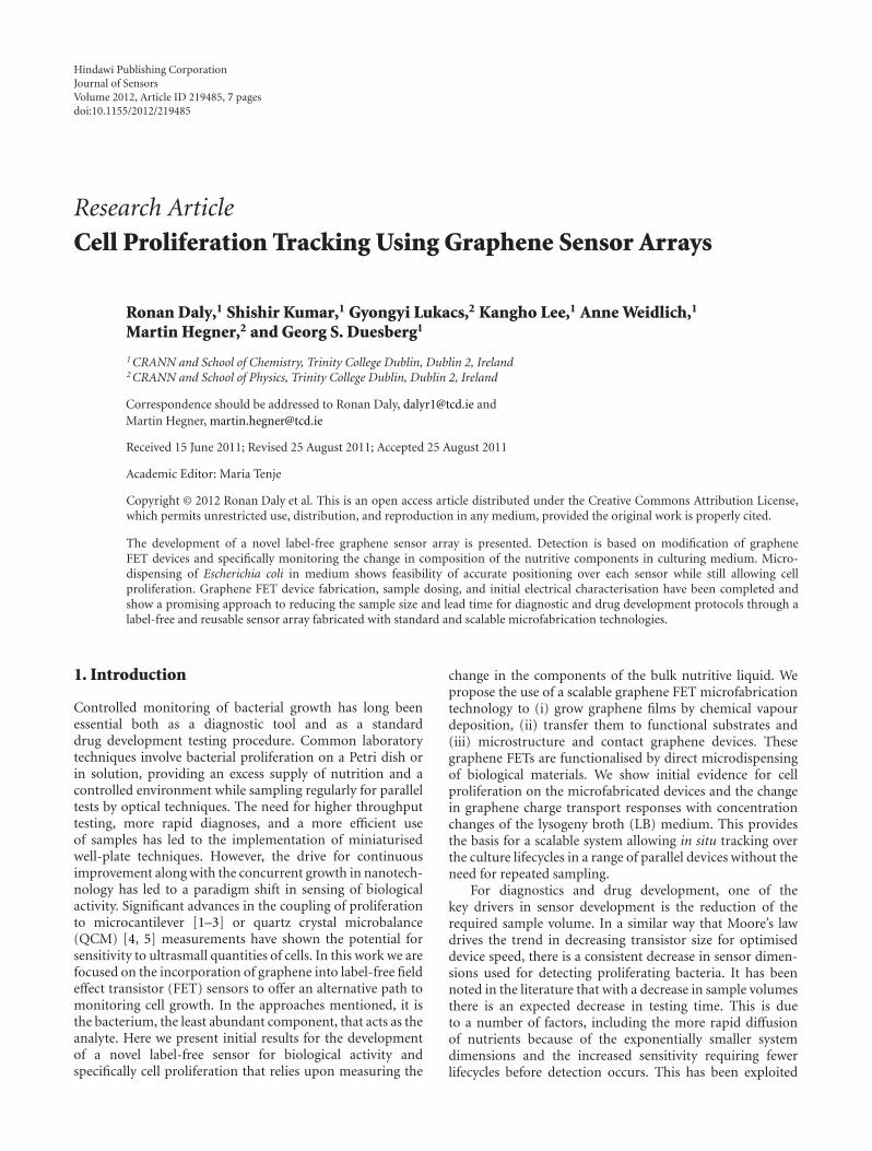
Figure 1: Metal electrodes contacting an underlying graphene layeracting as a sensor device with (a) bacteria proliferation occurringwithin a dosed volume of LB medium and (b) bacteria proliferationoccurring on a thin agar layer, filled with a nutritive medium.
previously using micromechanical approaches, for example,by Gfeller et al. [1] where bacteria grew on an agar layer ofa microcantilever array. However, these methods still havesome drawbacks, namely, multistep fabrication techniqueswith limited device reusability and intricate surroundingmeasurement apparatus. For the devices proposed in thiswork, as shown in Figure 1, the sensor area is in completecontact with the sample and, through rapid diffusion andconvection in such small sample volumes, is expected tobe highly sensitive to changes. Large arrays of these sensorsenable multiple parallel testing and improvement of thestatistical confidence while still decreasing the batch timeand conserving the low sample volume requirements. Therobust nature of the graphene FETs allows repeated cleaningand reuse while the output is a simple electrical resistancemeasurement in the kΩ range. In standard laboratory tech-niques and the microfabricated devices shown in Figure 1,LB is used as a feedstock to promote the binary fissionprocess and bacterial growth on an agar layer or in solution.The nutrition contained within the aqueous broth includesvitamins, minerals, and organic compounds such as aminoacids all of which are essential to the proliferation and growthof Escherichia coli (E. coli), the bacteria examined in thisreport.
The growth of cells is most often monitored by opticaldensity (OD) measurements, where light absorption is usedto identify the presence of bacteria in suspension. Thereare bulk-scale techniques to monitor the change in the LBcontent as a means to understanding the growth rate ofbacteria. These track solution conductivity, pH, or fluores-cence [6], but there are to-date limited attempts to scale thisapproach down to microscale arrays and to our knowledgeno attempts to incorporate two-dimensional carbon sensorsfor this purpose. The unique electrical and mechanicalproperties of graphene lend themselves to incorporation intoFET devices in this case. The relative freedom from catalyticimpurities, the low levels of noise, flexibility, robustness, andease of microstructuring have all been noted [7] as benefits tousing this material as an ultrasensitive recognition element inbiosensor devices. Such devices have proven effective in airand liquids for the sensing of individual gas molecules [8],proteins [9], and bacteria [10] when direct graphene-analyteinteractions occur. The direct contact is believed to lead tocharge transfer and hence a change in the electrical responseof the graphene sheet.
2. Experimental Details
2.1. Sensor Fabrication. Sensor devices are manufacturedon 15 × 15 mm pieces of p-doped (Boron) silicon (100)with a 300 nm layer of SiO2 from Si-Mat Silicon Materials,Germany, and cut using the Disco DAD 3220 wafer dicer.Samples are cleaned prior to microfabrication using ultra-sonication in HPLC grade acetone, ultrasonication and rinsein HPLC grade propan-2-ol and subsequent drying in a rapidflow of filtered, dry nitrogen. An oxygen plasma treatment isalso carried out to remove organic contamination using theDiener PICO barrel asher. Masks for UV lithography weredesigned in-house and created using the Heidelberg DWL66FS direct writing system. UV lithography was carried outwith the OAI Mask Aligner using Microposit S1813 positivephoto resist and MF319 developer (both from Rohm andHaas Electronic Materials). Metal sputter deposition wascarried out using the Gatan 682 Precision Etching CoatingSystem at a rate of 0.1 A s−1. After standard polymer lift-offprocedures, residual polymer was removed by oxygen plasmatreatment except when graphene was present, when solventcleaning alone was used.
2.2. Graphene Transfer and Etching. Graphene, produced bychemical vapour deposition (CVD) as described in Results, istransferred from metal foil to the substrate as follows. A layerof poly(methyl methacrylate) (PMMA), (Mr-I 35 K PMMAfrom Microresist Technology GmBH) was spin coated ontop of graphene film/copper foil pieces. Thermal-releasetape was adhered on top of this PMMA support film,and the copper was then etched by floating the sample inetchant (0.25 M FeCl3 + 0.2 M HCl). The resulting layeredfilm of thermal-release tape/PMMA/graphene was cleanedwith DI water, dried, and placed onto the substrate (asshown in Figure 3(b)). Because the graphene follows thecontours of the PMMA/thermal-release tape layer, a uniformpressure was applied to the film to ensure close contact andconformation to the substrate. A range of pressures wereused successfully ranging from 10 to 25 bar approximately.Heating the substrate from below promoted release of theupper tape layer. The remaining PMMA layer was removedby an initial soak in HPLC-grade acetone followed by anovernight soak in HPLC grade chloroform. The process canbe carried out without thermal-release tape to avoid somecontamination. In this case, PMMA-supported graphene isdredged from DI water onto the substrate. After the sampledries, PMMA can be removed as before.
2.3. Chemicals and Bacterial Culture. Chemicals and cul-turing medium were purchased from Sigma Aldrich (Ark-low, Ireland) unless otherwise stated. E. coli CIP 53.126was obtained from Collection de l’Institut Pasteur (Paris,France). Overnight cultures were prepared (200 rpm, 35◦C,15–18 h) in LB (1% NaCl, 1% tryptone, 0.5% yeast extract)from single colonies of E. coli. 1 mL of the overnight cultureswere transferred into 30 mL of 50% LB, and 25% glycerol,25% DI water and cultured (200 rpm, 35◦C) for 110 min inorder to reach a logarithmic growth rate. Glycerol was added
Journal of Sensors 3
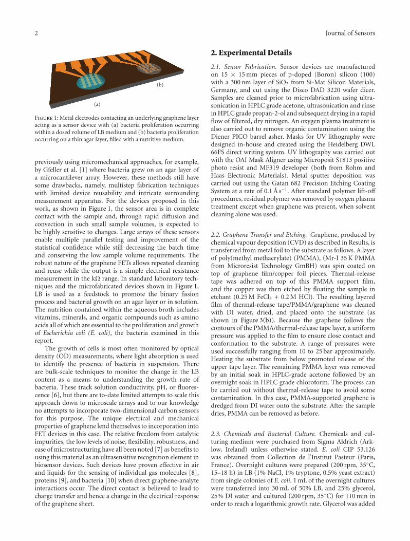
Pristine DI water LB 1%w/w LB 10%w/w LB
Diracpoint +10 V +4 V −17 V −34 V −43 V
44
45
46
47
48
49
50
51
−60 −40 −20 0 20 40 60
Cu
rren
t(µ
A)
Gate voltage (V)
(A) Pristine(B) DI water and dry
(C) LB and dry
Figure 2: Performing gate sweep using back-gated graphene FET device shows that with exposure to LB medium there is a shift in the Diraccurve towards the negative bias voltage.
to ensure droplets did not evaporate prior to measurement.Observations confirmed evaporation was inhibited. Twoadditional diluted solutions were prepared from the LB stock.The first solution consisted of 500 µL LB, 250 µL glycerol, and250 µL DI water. The second, more dilute solution consistedof 31 µL LB, 250 µL glycerol, and 469 µL deionised water(twice dilution and thirty-two times dilution, resp.). Theseare referred to as 2LB and 32LB in the text.
2.4. Microdispensing and Electrical Measurement. LB me-dium both with and without cells was dosed during this workusing an Autodrop microdispensing system from MicrodropTechnologies and a nozzle with a diameter of 50 µm.Subsequent electrical measurements on the graphene FETdevices were carried out using a Keithley 2400 Sourcemeterattached to a Karl Suss probe station. Substrates weretransferred between the dosing and measurement deviceswithin a Petri dish containing a pad saturated with waterto maintain humidity and inhibit evaporation of the doseddroplets during transport.
2.5. Additional Analysis. Raman spectroscopy was carriedout using a Horriba Jobin Yvon LabRam HR system and aline of 632.8 nm. Scanning electron microscopy (SEM) wascarried out using the Zeiss ULTRA Plus in the AdvancedMicroscopy Laboratory, CRANN, Trinity College Dublin.Prior to SEM imaging, bacteria were fixed by soakingin 5% v/v glutaraldehyde solution in 0.05 M phosphatebuffer (pH7) and incubated at room conditions with gentleagitation for 3-4 h. Glutaraldehyde was then removed by 6successive washes in fresh 0.05 M phosphate buffer, each of10 minutes duration. Samples were subsequently dehydratedwith a sequence of 10-minute rinses in 10, 30, 50, 70, 90, 100,and 100% v/v ethanol.
3. Results and Discussion
The fundamental premise of LB components affecting theconductance of graphene was confirmed using high-qualitygraphene flakes grown on Ni by chemical vapour deposi-tion (CVD) and contacted with e-beam lithography. Thegraphene preparation and contacting process is describedelsewhere [11]. The crucial step in this case is that thegraphene has been cleaved by the Scotch tape to leave a cleansurface. By dosing (i) 18 MΩ deionised water and (ii) LBmedium onto a graphene FET device and comparing theelectrical response of the sensor upon solvent evaporation,we see the precipitated materials from the LB mediumlead to a slight increase in the measured resistance of thegraphene strips and a clear shift in the Dirac point, asindicated in Figure 2. Graphene has linear dispersion inboth valence and conduction bands. The degenerate pointwhere these bands meet is known as the Dirac point. TheFermi level of graphene can move across the Dirac pointunder a bias, changing the concentration of charge carriersand therefore the resistance of samples. Thus, the minimumconductance (or maximum resistance) point observed in I–Vcharacteristics displayed in Figure 2 corresponds to the Diracpoint. A negative shift, as is observed for the samples exposedto LB, is equivalent to n-doping of the graphene.
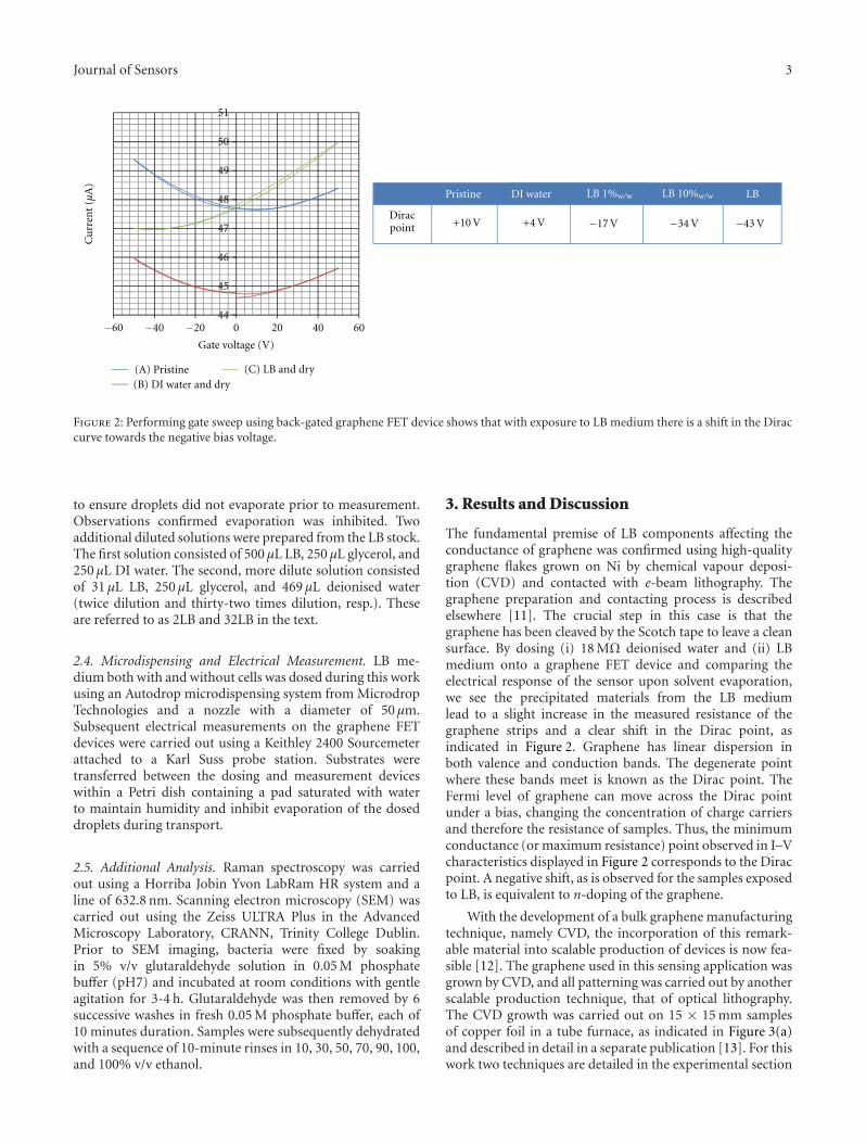
With the development of a bulk graphene manufacturingtechnique, namely CVD, the incorporation of this remark-able material into scalable production of devices is now fea-sible [12]. The graphene used in this sensing application wasgrown by CVD, and all patterning was carried out by anotherscalable production technique, that of optical lithography.The CVD growth was carried out on 15 × 15 mm samplesof copper foil in a tube furnace, as indicated in Figure 3(a)and described in detail in a separate publication [13]. For thiswork two techniques are detailed in the experimental section
4 Journal of Sensors
CH4/H2 flow
Graphene
Copper
(a)
Thermal release tapePMMA
Graphene
Si substrate
Pressure applied
Heated substrate
(b)
Ni pattern to protect graphene
(c)
oxygen plasma etchingGraphene patterns formed by
(d)
Graphene strips contacted byNi/Au electrodes
20 µm
(e)
Devices can be wire-bonded to
chip carrier for analysis
(f)
Figure 3: Production and microfabrication of graphene. (a) CVD growth of graphene on copper foil in a tube furnace, (b) graphene isattached to SiO2/Si by attaching to a support layer of PMMA and thermal-release tape and transferring by a combination of heat andpressure, (c) after transfer to SiO2/Si substrate, a Ni protection layer is patterned on the graphene, (d) oxygen plasma removes the unprotectedgraphene and the Nickel is subsequently removed by HCl etching. (e) shows the contacted graphene strips and (f) shows integration of thesensor into a chip carrier.
attempting to optimise the transfer of approximately 15 ×15 mm films of graphene to the SiO2/Si substrates. In sum-mary, after coating the graphene film/copper foil pieces witha PMMA support layer and a further layer of thermal releasetape, the copper can be removed by etching with FeCl3.Transfer of graphene to SiO2/Si substrates is completed byapplying pressure through the tape and PMMA supportlayers, pressing the graphene surface onto the substrate asindicated in Figure 3(b). Heat applied through the substrateallows easy release of the thermal-release tape leaving behindthe PMMA/graphene layers with the graphene adhering tothe substrate very strongly by the van der Waals forces [14].The PMMA can be removed with solvent cleaning. Due toconcerns regarding contamination from the thermal-releasetape and the fracturing effects of the mechanical transfermethod, a second approach was developed. The PMMAsupport layer is still applied to the graphene film/copperfoil pieces and the etching occurs as before at the liquid-air interface, leaving a graphene/PMMA layer floating onthe surface. This is carefully transferred to the substratesurface through dip coating, and the same solvent cleaningsteps occur to remove PMMA. The substrates have beenprestructured by UV lithography with distinct, chromiumalignment marks. These were included to enable a sequence
of UV lithography patterning steps to occur that lead tometal-contacted graphene strips with good adhesion to thesubstrate, using a technique described by Kumar et al.,[13]. As shown in Figures 3(c)–3(f), a sacrificial maskingpattern of nickel is formed to protect the areas requiredfor the devices and the uncovered graphene is removed byan oxygen plasma. The nickel protection layers are thencompletely removed by an acid etch with 1 M HCl, andthe remaining graphene strips are contacted by four Ni/Auelectrodes (4 µm/48 µm) using a final UV lithography step.The contacted samples can then be probed directly using aneedle prober or wire-bonded to a chip carrier for electricalmeasurements. This technique was modified from previouswork to include a range of alignment marks for accuratepositioning of all layers and a design that can be directlyincorporated into an inkjet dosing system.
It is observed that the gate voltage behaviour and thescale of resistances recorded for graphene prepared with thistechnique have changed. This is partly due to the known issueof contamination during the incorporation of graphene intofunctional devices using multistep lithography processes.Graphene is notoriously difficult to maintain free of con-tamination and defects, and novel cleaning techniques willbecome essential for large-scale manufacture of graphene
Journal of Sensors 5
0
200
400
600
800
1000
1200
1400
1100 1600 2100 2600
Inte
nsi
ty
Frequency (cm−1)
2D
D
G
(a)(b)
1.5
2
2.5
3
3.5
4
4.5
−70 −50 −30 −10 10 30 50 70
Gate voltage (V)
(A) Pristine(B) 3% v/v LB(C) 21% v/v LB(D) 29% v/v LB
(E) 33% v/v LB(F) 36% v/v LB(G) 38% v/v LB
Sou
rce-
drai
nC
urr
ent
(µA
)
(c)
16
17
18
19
20
21
22
0 5 10 15 20 25 30 35 40
Res
ista
nce
(kΩ
)
Concentration of LB (% v/v)
(d)
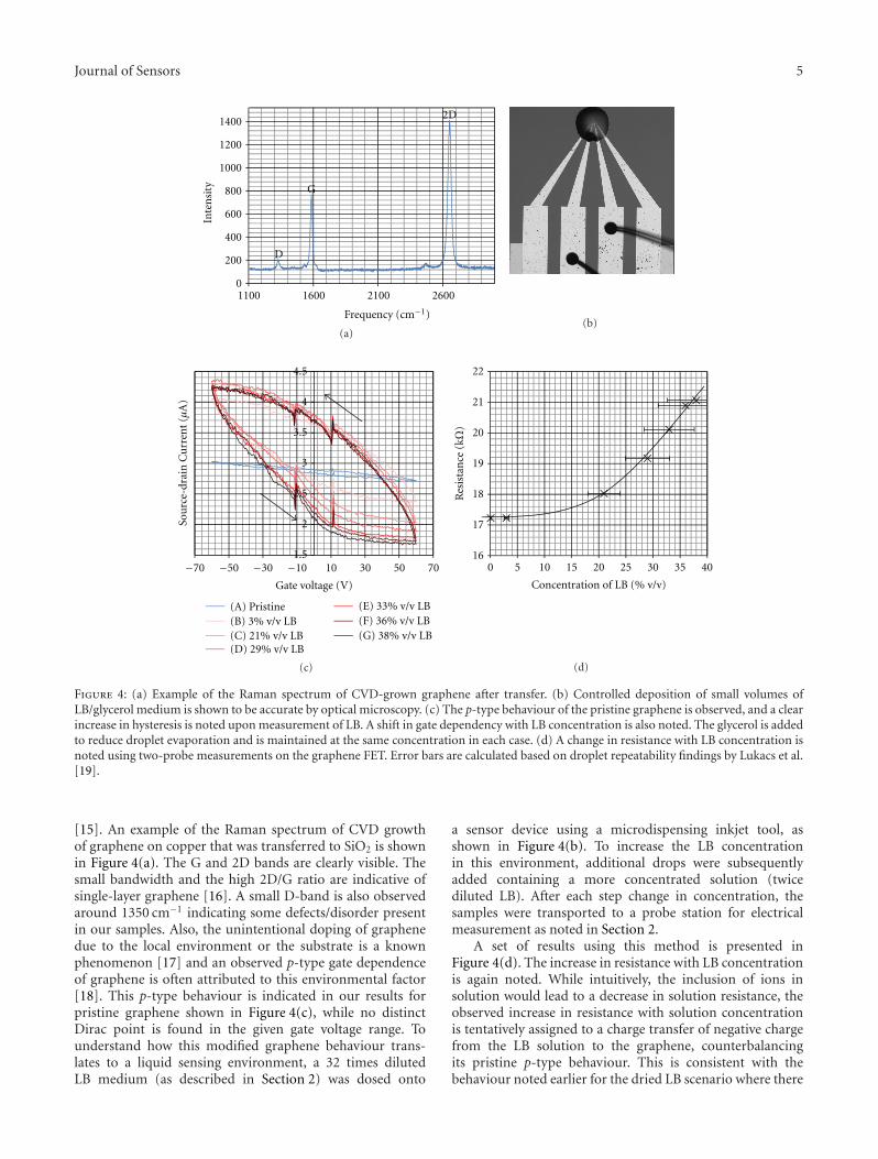
Figure 4: (a) Example of the Raman spectrum of CVD-grown graphene after transfer. (b) Controlled deposition of small volumes ofLB/glycerol medium is shown to be accurate by optical microscopy. (c) The p-type behaviour of the pristine graphene is observed, and a clearincrease in hysteresis is noted upon measurement of LB. A shift in gate dependency with LB concentration is also noted. The glycerol is addedto reduce droplet evaporation and is maintained at the same concentration in each case. (d) A change in resistance with LB concentration isnoted using two-probe measurements on the graphene FET. Error bars are calculated based on droplet repeatability findings by Lukacs et al.[19].
[15]. An example of the Raman spectrum of CVD growthof graphene on copper that was transferred to SiO2 is shownin Figure 4(a). The G and 2D bands are clearly visible. Thesmall bandwidth and the high 2D/G ratio are indicative ofsingle-layer graphene [16]. A small D-band is also observedaround 1350 cm−1 indicating some defects/disorder presentin our samples. Also, the unintentional doping of graphenedue to the local environment or the substrate is a knownphenomenon [17] and an observed p-type gate dependenceof graphene is often attributed to this environmental factor[18]. This p-type behaviour is indicated in our results forpristine graphene shown in Figure 4(c), while no distinctDirac point is found in the given gate voltage range. Tounderstand how this modified graphene behaviour trans-lates to a liquid sensing environment, a 32 times dilutedLB medium (as described in Section 2) was dosed onto
a sensor device using a microdispensing inkjet tool, asshown in Figure 4(b). To increase the LB concentrationin this environment, additional drops were subsequentlyadded containing a more concentrated solution (twicediluted LB). After each step change in concentration, thesamples were transported to a probe station for electricalmeasurement as noted in Section 2.
A set of results using this method is presented inFigure 4(d). The increase in resistance with LB concentrationis again noted. While intuitively, the inclusion of ions insolution would lead to a decrease in solution resistance, theobserved increase in resistance with solution concentrationis tentatively assigned to a charge transfer of negative chargefrom the LB solution to the graphene, counterbalancingits pristine p-type behaviour. This is consistent with thebehaviour noted earlier for the dried LB scenario where there
6 Journal of Sensors
100 µm
(a)
1 µm
(b)
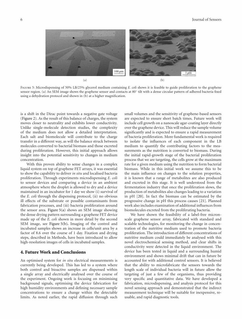
Figure 5: Microdispensing of 50% LB/25% glycerol medium containing E. coli shows it is feasible to guide proliferation to the graphenesensor region. (a) An SEM image shows the graphene sensor and contacts at 80◦ tilt with a dense circular pattern of adhered bacteria fixedusing a dehydration protocol and shown in (b) at a higher magnification.
is a shift in the Dirac point towards a negative gate voltage(Figure 2). As the result of this balance of charges, the systemmoves closer to neutrality and exhibits lower conductivity.Unlike single-molecule detection studies, the complexityof the medium does not allow a detailed interpretation.Each salt and biomolecule will contribute to the chargetransfer in a different way, as will the balance struck betweenmolecules converted to bacterial biomass and those excretedduring proliferation. However, this initial approach allowsinsight into the potential sensitivity to changes in mediumconcentration.
With this proven ability to sense changes in a complexliquid system on top of graphene FET arrays, it was essentialto show the capability to deliver in situ and localised bacteriaproliferation. Through experiments microdispensing E. colito sensor devices and comparing a device in an ambientatmosphere where the droplet is allowed to dry and a devicemaintained in an incubator for 1 day we show (i) survival ofthe E. coli through the dispensing protocol, (ii) no obviousill effects of the substrate or possible contaminants fromfabrication processes, and (iii) bacteria proliferation aroundthe sensor area. Figure 5(a) shows an SEM image showingthe dense drying pattern surrounding a graphene FET devicemade up of the E. coli shown in more detail by the secondSEM image, see Figure 5(b). Imaging of the control andincubated samples shows an increase in cells/unit area by afactor of 8.6 over the course of 1 day. Fixation and dryingsteps, described in Methods, have been introduced to allowhigh-resolution images of cells in incubated samples.
4. Future Work and Conclusions
An optimised system for in situ electrical measurements iscurrently being developed. This has led to a system whereboth control and bioactive samples are dispensed withina single array and electrically analysed over the course ofthe experiment. Ongoing work is focusing on minimisingbackground signals, optimising the device fabrication forhigh humidity environments and defining necessary sampleconcentrations to ensure a change within the detectablelimits. As noted earlier, the rapid diffusion through such
small volumes and the sensitivity of graphene-based sensorsare expected to ensure short batch times. Future work willinclude cell growth on a nanoscale agar-coating layer directlyover the graphene device. This will reduce the sample volumesignificantly and is expected to ensure a rapid measurementof bacteria proliferation. More fundamental work is requiredto isolate the influences of each component in the LBmedium to quantify the contributing factors to the mea-surements as the nutrition is converted to biomass. Duringthe initial rapid-growth stage of the bacterial proliferationprocess that we are targeting, the cells grow at the maximumrate for a given medium using the nutrition to form bacterialbiomass. While in this initial work we assume this to bethe main influence on changes to the solution properties,it is known that a range of metabolites are also producedand excreted in this stage. It is well understood from thefermentation industry that once the proliferation slows, theproduction of metabolites also changes leading to a variationin pH [20]. In fact the biomass can be estimated by theprogressive change in pH this process causes [21]. Plannedwork also includes examination of additional influences frombiomolecules excreted from the proliferating bacteria.
We have shown the feasibility of a label-free micron-scale graphene sensor array, fabricated with standard andscalable technologies, for monitoring the change in concen-tration of the nutritive medium used to promote bacteriaproliferation. The introduction of different concentrations ofnutritive medium could immediately be analysed with thisnovel electrochemical sensing method, and clear shifts inconductivity were detected in the liquid environment. Thedevice has been tested in liquid and a surrounding humidenvironment and shows minimal drift that can in future beaccounted for with additional control sensors. It is believedthat the ability to microfabricate the sensors towards thelength scale of individual bacteria will in future allow thetargeting of just a few of the organisms, thus providingvery specific and quantitative data. We have developed afabrication, microdispensing, and analysis protocol for thisnovel sensing approach and demonstrated that the indirectmeasurement technique will be suitable for inexpensive, re-usable, and rapid diagnostic tools.
Journal of Sensors 7
Acknowledgments
This work was supported by the Science Foundation Irelandunder the CSET scheme SFI08/CE/I1432. The SEM imagingwas enabled by the Advanced Microscopy Laboratory, TrinityTechnology and Enterprise Campus, Dublin 2, Ireland underthe framework of the INSPIRE programme, funded by theIrish Government’s Programme for Research in Third LevelInstitutions, Cycle 4, National Development Plan 2007–2013.GSD acknowledges SFI for the PICA grant and SK theEmbark Initiative for an IRCSET scholarship.
References
[1] K. Y. Gfeller, N. Nugaeva, and M. Hegner, “Rapid biosensor fordetection of antibiotic-selective growth of Escherichia coli,”Applied and Environmental Microbiology, vol. 71, no. 5, pp.2626–2631, 2005.
[2] D. Ramos, J. Tamayo, J. Mertens, M. Calleja, and A. Zaballos,“Origin of the response of nanomechanical resonators tobacteria adsorption,” Journal of Applied Physics, vol. 100, no.10, Article ID 106105, pp. 106105-1–106105-3, 2006.
[3] N. Nugaeva, K. Y. Gfeller, N. Backmann, H. P. Lang, H. J.Guntherodt, and M. Hegner, “An antibody-sensitized micro-fabricated cantilever for the growth detection of Aspergillusniger spores,” Microscopy and Microanalysis, vol. 13, no. 1, pp.13–17, 2007.
[4] N. Kim and I. S. Park, “Application of a flow-type antibodysensor to the detection of Escherichia coli in various foods,”Biosensors and Bioelectronics, vol. 18, no. 9, pp. 1101–1107,2003.
[5] X. L. Su and Y. Li, “A QCM immunosensor for Salmonelladetection with simultaneous measurements of resonant fre-quency and motional resistance,” Biosensors and Bioelectronics,vol. 21, no. 6, pp. 840–848, 2005.
[6] C. Faber, “Assessment of the inhibitory potency by MRI,” inNMR Spectroscopy in Pharmaceutical Analysis, U. Holzgrabe etal., Ed., Elsevier, 2008.
[7] W. Yang, K. R. Ratinac, S. R. Ringer, P. Thordarson, J. J.Gooding, and F. Braet, “Carbon nanomaterials in biosen-sors: Should you use nanotubes or graphene,” AngewandteChemie—International Edition, vol. 49, no. 12, pp. 2114–2138,2010.
[8] F. Schedin, A. K. Geim, S. V. Morozov et al., “Detectionof individual gas molecules adsorbed on graphene,” NatureMaterials, vol. 6, no. 9, pp. 652–655, 2007.
[9] Y. Ohno, K. Maehashi, Y. Yamashiro, and K. Matsumoto,“Electrolyte-gated graphene field-effect transistors for detect-ing ph and protein adsorption,” Nano Letters, vol. 9, no. 9, pp.3318–3322, 2009.
[10] N. Mohanty and V. Berry, “Graphene-based single-bacteriumresolution biodevice and DNA transistor: Interfacinggraphene derivatives with nanoscale and microscalebiocomponents,” Nano Letters, vol. 8, no. 12, pp. 4469–4476, 2008.
[11] P. N. Nirmalraj, T. Lutz, S. Kumar, G. S. Duesberg, and J.J. Boland, “Nanoscale mapping of electrical resistivity andconnectivity in graphene strips and networks,” NanoLetters,vol. 11, pp. 16–22, 2011.
[12] X. Li, W. Cai, J. An et al., “Large-area synthesis of high-qualityand uniform graphene films on copper foils,” Science, vol. 324,no. 5932, pp. 1312–1314, 2009.
[13] S. Kumar, N. Peltekis, K. Lee, H. Kim, and G. S. Duesberg,“Reliable processing of graphene using metal etchmasks,”Nanoscale Research Letters, vol. 6, no. 1, p. 390, 2011.
[14] J. S. Bunch, S. S. Verbridge, J. S. Alden et al., “Impermeableatomic membranes from graphene sheets,” Nano Letters, vol.8, no. 8, pp. 2458–2462, 2008.
[15] N. Peltekis, S. Kumar, N. McEvoy, K. Lee, A. Weidlich, and G.S. Duesberg, “The effect of downstream plasma treatments ongraphene surfaces,” Carbon, vol. 50, no. 2, pp. 395–403, 2012.
[16] A. C. Ferrari, J. C. Meyer, V. Scardaci et al., “Raman spectrumof graphene and graphene layers,” Physical Review Letters, vol.97, no. 18, Article ID 187401, 2006.
[17] Y. H. Wu, T. Yu, and Z. X. Shen, “Two-dimensional carbonnanostructures: fundamental properties, synthesis, character-ization, and potential applications,” Journal of Applied Physics,vol. 108, no. 7, Article ID 071301, 2010.
[18] H. E. Romero, N. Shen, P. Joshi et al., “n-type behavior ofgraphene supported on Si/SiO2 substrates,” ACS Nano, vol. 2,no. 10, pp. 2037–2044, 2008.
[19] G. Lukacs, N. Maloney, and M. Hegner, “Ink-jet printing: per-fect tool for cantilever array sensor preparation for microbialgrowth detection,” Journal of Sensors. In press.
[20] M. Scheidle, B. Dittrich, J. Klinger, H. Ikeda, D. Klee, and J.Buchs, “Controlling pH in shake flasks using polymer-basedcontrolled-release discs with pre-determined release kinetics,”BMC Biotechnology, vol. 11, p. 25, 2011.
[21] M. L. Christensen and N. T. Eriksen, “Growth and protonexchange in recombinant Escherichia coli BL21,” Enzyme andMicrobial Technology, vol. 31, no. 4, pp. 566–574, 2002.