challenges probing next generation full array … probing next generation full array products with...
TRANSCRIPT
Challenges probing next generation full array products with 60 µm
pitch and below
Presenter: Raffaele Vallauri – Technoprobe
Co-authors: Erik Jan Marinissen – IMEC Jerry Broz – ITS
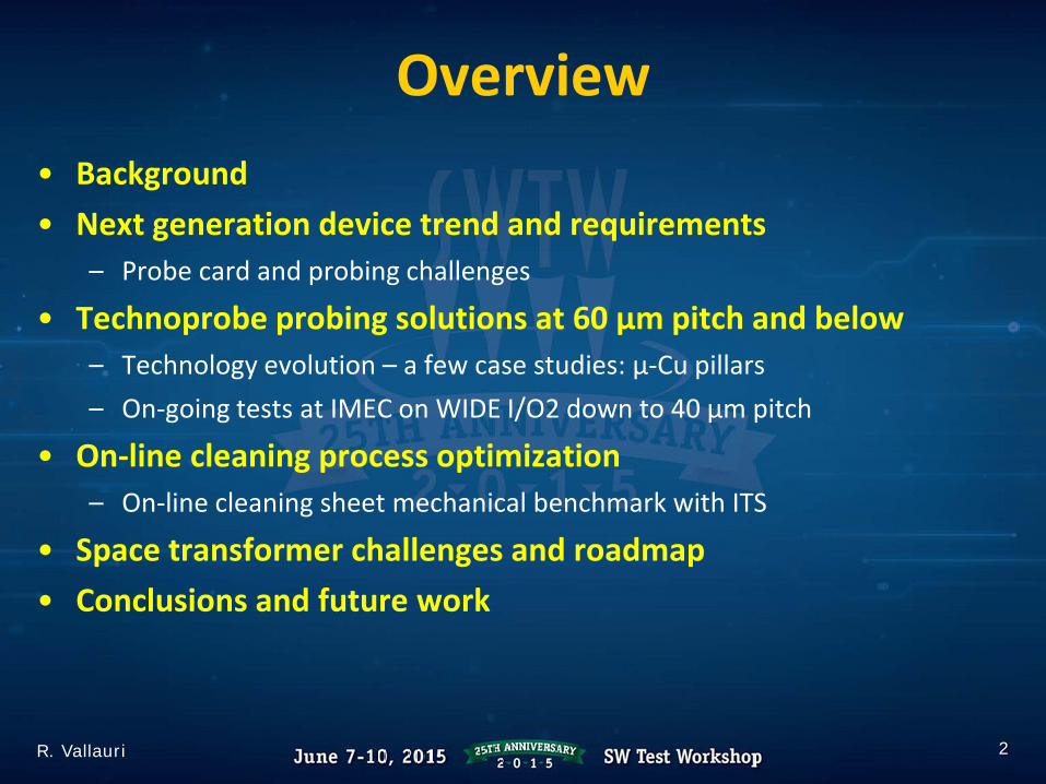
Overview• Background• Next generation device trend and requirements
– Probe card and probing challenges
• Technoprobe probing solutions at 60 µm pitch and below– Technology evolution – a few case studies: µ-Cu pillars– On-going tests at IMEC on WIDE I/O2 down to 40 µm pitch
• On-line cleaning process optimization – On-line cleaning sheet mechanical benchmark with ITS
• Space transformer challenges and roadmap• Conclusions and future work
2R. Vallauri
Background• Over the last 3-4 years, the requirements of probing dense
arrays of bumps have been more and more demanding
• To address our customers needs we have been developing new approaches in probing and space transformer technologies (presented at SWTW 2013-14) introducing:– TPEG™ MEMS T3, to overcome all limitations of previous Cobra-like
technologies (SWTW 2013)– TPEG™ MEMS T1, to allow probe on µ-Cu pillar bumps (SWTW 2014)
• Furthermore, understanding the overall industry needs is a critical step to translate our customers’ next generation challenges in probe cards evolution
3R. Vallauri
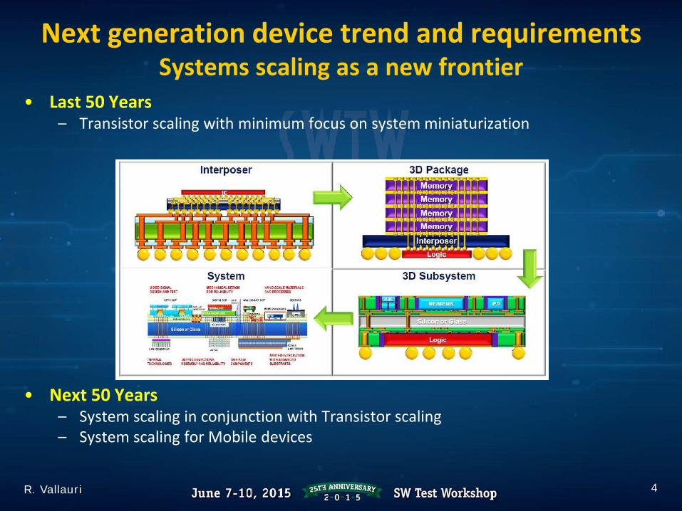
Next generation device trend and requirementsSystems scaling as a new frontier
• Last 50 Years– Transistor scaling with minimum focus on system miniaturization
• Next 50 Years– System scaling in conjunction with Transistor scaling– System scaling for Mobile devices
4R. Vallauri
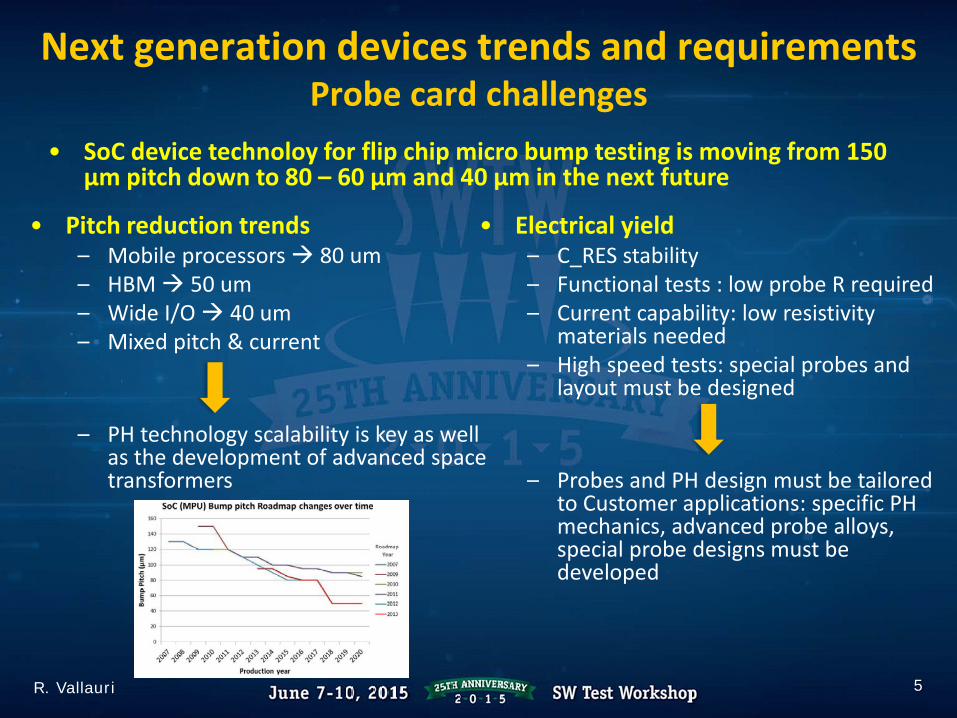
• Pitch reduction trends– Mobile processors 80 um– HBM 50 um– Wide I/O 40 um– Mixed pitch & current
– PH technology scalability is key as well as the development of advanced space transformers
Next generation devices trends and requirementsProbe card challenges
5
• SoC device technoloy for flip chip micro bump testing is moving from 150 µm pitch down to 80 – 60 µm and 40 µm in the next future
• Electrical yield – C_RES stability– Functional tests : low probe R required– Current capability: low resistivity
materials needed– High speed tests: special probes and
layout must be designed
– Probes and PH design must be tailored to Customer applications: specific PH mechanics, advanced probe alloys, special probe designs must be developed
R. Vallauri
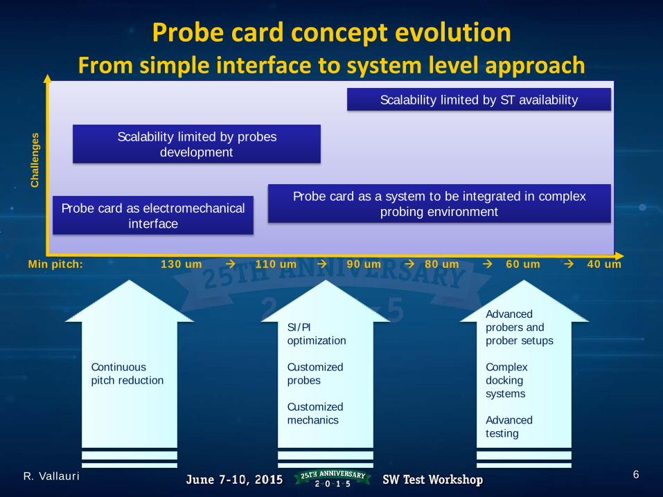
Probe card concept evolutionFrom simple interface to system level approach
6
Continuous pitch reduction
SI/PI optimization
Customized probes
Customized mechanics
Advanced probers and prober setups
Complex docking systems
Advanced testing
Min pitch: 130 um 110 um 90 um 80 um 60 um 40 um
Probe card as electromechanical interface
Probe card as a system to be integrated in complex probing environment
Scalability limited by ST availability
Scalability limited by probes development
Cha
lleng
es
R. Vallauri
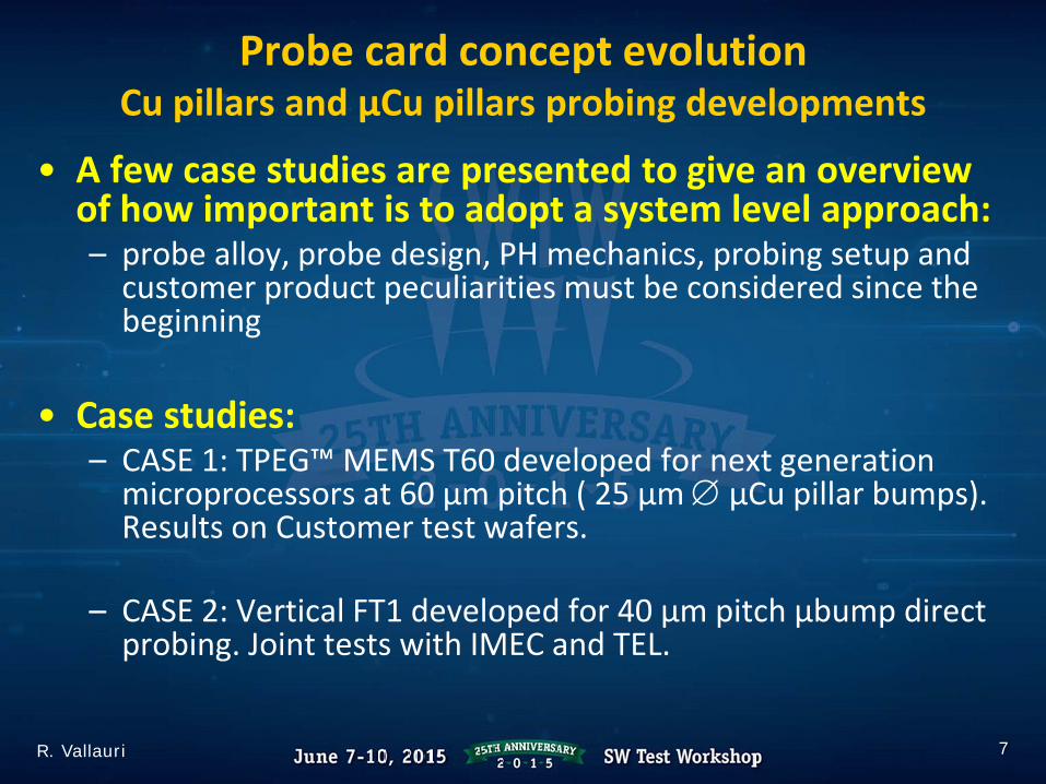
• A few case studies are presented to give an overview of how important is to adopt a system level approach: – probe alloy, probe design, PH mechanics, probing setup and
customer product peculiarities must be considered since the beginning
• Case studies:– CASE 1: TPEG™ MEMS T60 developed for next generation
microprocessors at 60 µm pitch ( 25 µm ∅ µCu pillar bumps). Results on Customer test wafers.
– CASE 2: Vertical FT1 developed for 40 µm pitch µbump direct probing. Joint tests with IMEC and TEL.
Probe card concept evolutionCu pillars and µCu pillars probing developments
7R. Vallauri
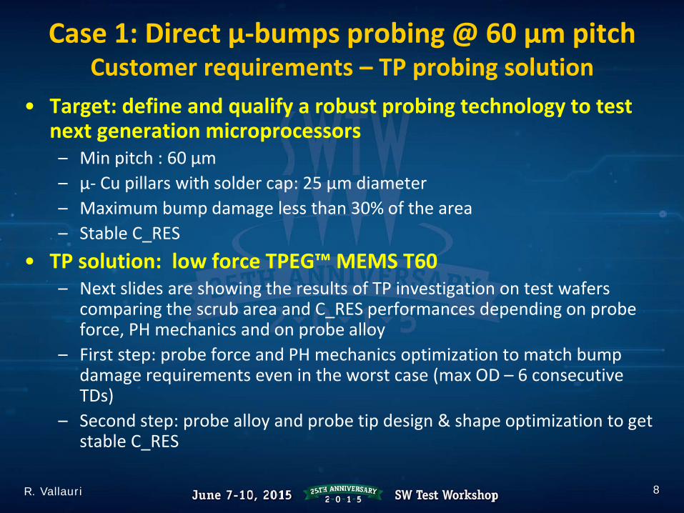
Case 1: Direct µ-bumps probing @ 60 µm pitchCustomer requirements – TP probing solution
• Target: define and qualify a robust probing technology to test next generation microprocessors– Min pitch : 60 µm– µ- Cu pillars with solder cap: 25 µm diameter– Maximum bump damage less than 30% of the area – Stable C_RES
• TP solution: low force TPEG™ MEMS T60– Next slides are showing the results of TP investigation on test wafers
comparing the scrub area and C_RES performances depending on probe force, PH mechanics and on probe alloy
– First step: probe force and PH mechanics optimization to match bump damage requirements even in the worst case (max OD – 6 consecutive TDs)
– Second step: probe alloy and probe tip design & shape optimization to get stable C_RES
8R. Vallauri
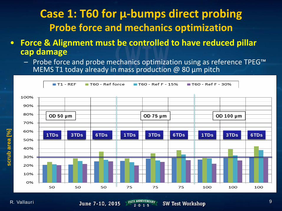
Case 1: T60 for µ-bumps direct probing Probe force and mechanics optimization
• Force & Alignment must be controlled to have reduced pillar cap damage– Probe force and probe mechanics optimization using as reference TPEG™
MEMS T1 today already in mass production @ 80 µm pitch
9
1TDs 3TDs 6TDs
OD 50 µm OD 75 µm OD 100 µm
scru
b ar
ea [%
]
3TDs 6TDs 1TDs 3TDs 6TDs 1TDs 3TDs 6TDs
R. Vallauri

Case 1: T60 for µ-bumps direct probing C_RES tests setup
• C_RES TESTS SETUP on Customer TV wfs– A few C_RES pairs available (in short @ wafer top metal level)
• Measurement principle: Force V – Measure I– Force V = 10 mV– Clamp I = 50 mA– R Pair = 0.5 x (V/I)
10R. Vallauri
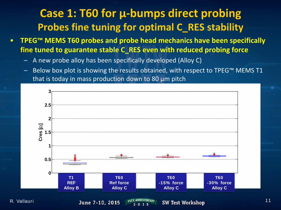
Case 1: T60 for µ-bumps direct probing Probes fine tuning for optimal C_RES stability
• TPEG™ MEMS T60 probes and probe head mechanics have been specifically fine tuned to guarantee stable C_RES even with reduced probing force
– A new probe alloy has been specifically developed (Alloy C)– Below box plot is showing the results obtained, with respect to TPEG™ MEMS T1
that is today in mass production down to 80 µm pitch
11
0
0.5
1
1.5
2
2.5
3
T1 REF (B) T60 REF (C) T60 -15% (C) T60 -30% (C)
Cre
s [ Ω
]
T1REF
Alloy B
T60Ref forceAlloy C
T60-15% force
Alloy C
T60-30% force
Alloy C
R. Vallauri
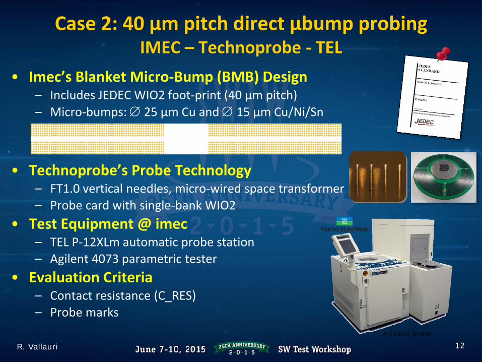
Case 2: 40 µm pitch direct µbump probingIMEC – Technoprobe - TEL
12
• Imec’s Blanket Micro-Bump (BMB) Design– Includes JEDEC WIO2 foot-print (40 µm pitch)– Micro-bumps: ∅ 25 µm Cu and ∅ 15 µm Cu/Ni/Sn
• Technoprobe’s Probe Technology– FT1.0 vertical needles, micro-wired space transformer– Probe card with single-bank WIO2
• Test Equipment @ imec– TEL P-12XLm automatic probe station– Agilent 4073 parametric tester
• Evaluation Criteria– Contact resistance (C_RES)– Probe marks
P-12XLm prober
R. Vallauri
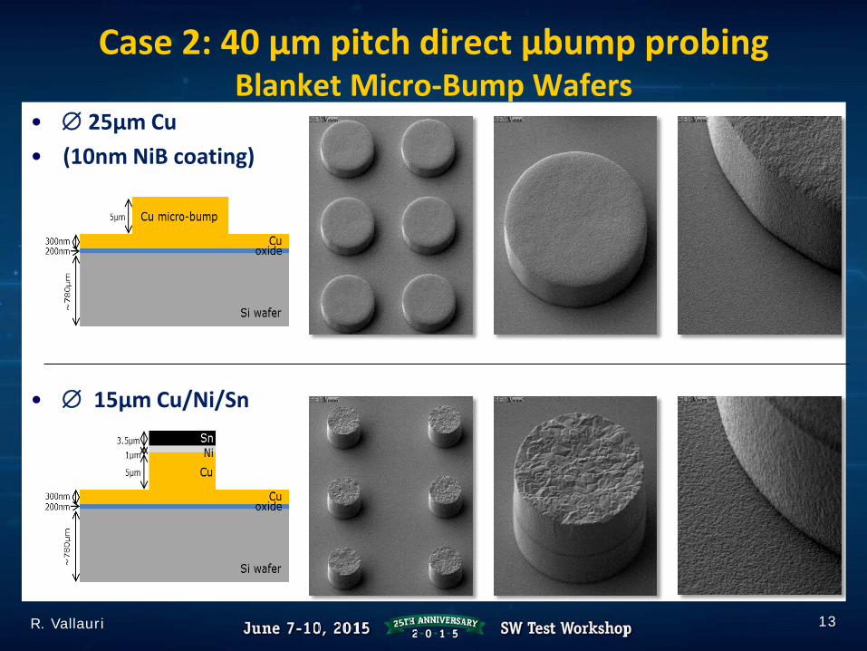
Case 2: 40 µm pitch direct µbump probingBlanket Micro-Bump Wafers
13
• ∅ 25µm Cu• (10nm NiB coating)
• ∅ 15µm Cu/Ni/Sn
R. Vallauri

Case 2: 40 µm pitch direct µbump probingInitial results with pointed tips
• Preliminary C_RES results with pointed tips are summarized here below.
• Pointed Tips, OT=75µm - Mean C_RES– Overall: 30.97 Ω– Zero dummy rings : 28.49 Ω– One dummy ring : 31.04 Ω– Two dummy rings : 33.38 Ω
• Pointed Tips, OT=85µm - Mean C_RES– Overall: 27.69 Ω– Zero dummy rings : 26.19 Ω– One dummy ring : 28.69 Ω– Two dummy rings : 28.18 Ω
14R. Vallauri

Case 2: 40 µm pitch direct µbump probingInitial results with flat tips
• First results with flat tips are reported below
15
D02
: Cu+
NiB
D03
: Cu
D04
: Cu/
Ni/
Sn
D03: Cu C_RES remains in range 4-50 Ω Mean* C_RES = 17.20 Ω
D04: Cu/Ni/Sn C_RES remains largely in range 4-6 Ω Mean* C_RES = 4.44 Ω Sn is a lot easier to probe than Cu
D02: Cu+NiB C_RES remains in range 4-50 Ω Mean* C_RES = 28.39 Ω Cu even harder to probe due to NiB
R. Vallauri
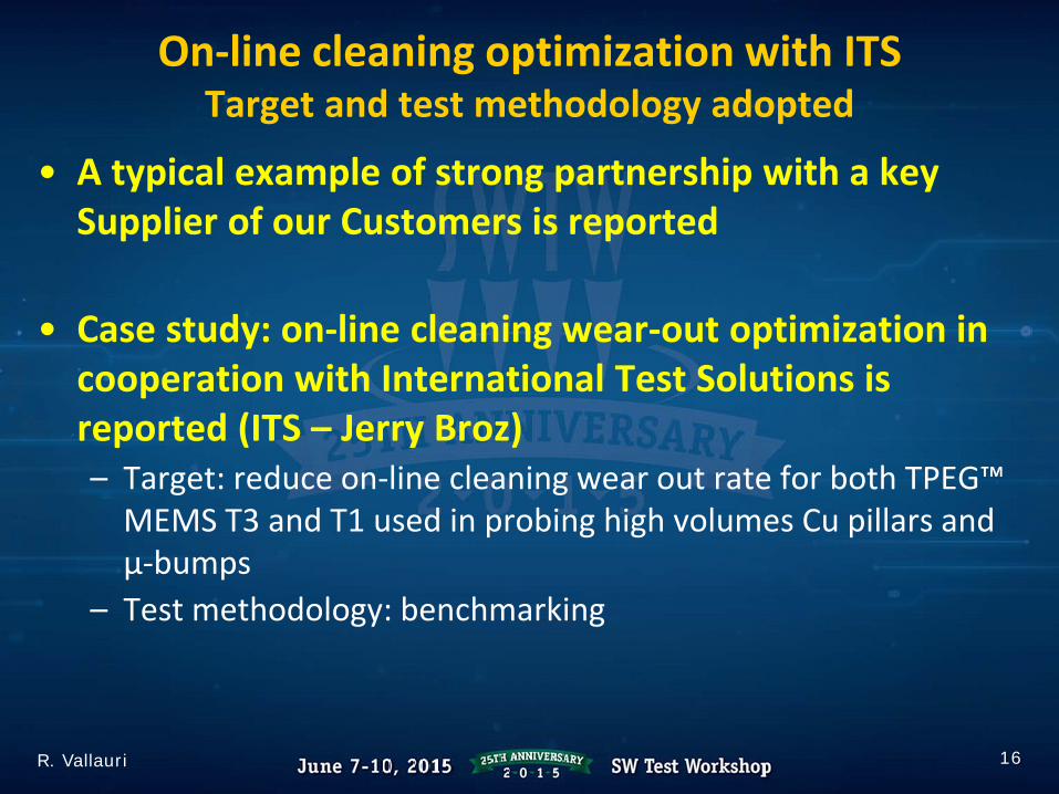
On-line cleaning optimization with ITSTarget and test methodology adopted
• A typical example of strong partnership with a key Supplier of our Customers is reported
• Case study: on-line cleaning wear-out optimization in cooperation with International Test Solutions is reported (ITS – Jerry Broz)– Target: reduce on-line cleaning wear out rate for both TPEG™
MEMS T3 and T1 used in probing high volumes Cu pillars and µ-bumps
– Test methodology: benchmarking
16R. Vallauri
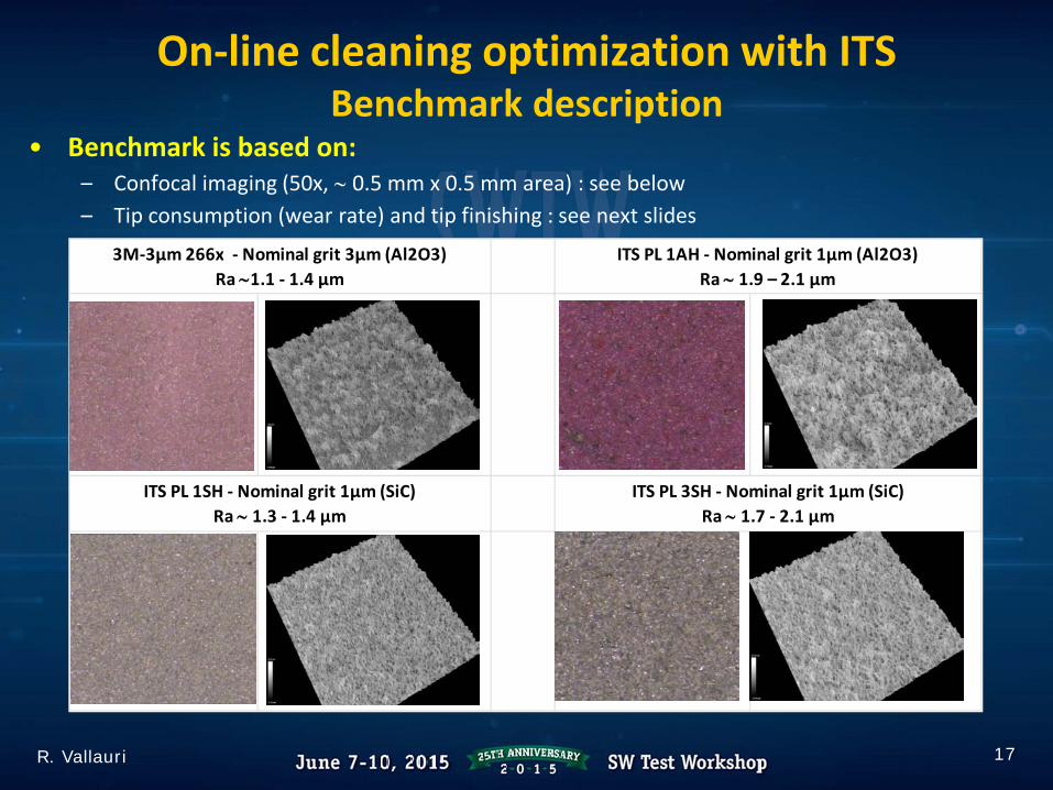
On-line cleaning optimization with ITSBenchmark description
• Benchmark is based on:– Confocal imaging (50x, ∼ 0.5 mm x 0.5 mm area) : see below– Tip consumption (wear rate) and tip finishing : see next slides
17R. Vallauri
3M-3µm 266x - Nominal grit 3µm (Al2O3)Ra ∼1.1 - 1.4 µm
ITS PL 1AH - Nominal grit 1µm (Al2O3)Ra ∼ 1.9 – 2.1 µm
ITS PL 1SH - Nominal grit 1µm (SiC)Ra ∼ 1.3 - 1.4 µm
ITS PL 3SH - Nominal grit 1µm (SiC)Ra ∼ 1.7 - 2.1 µm
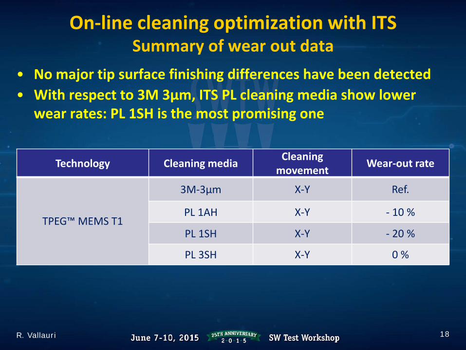
On-line cleaning optimization with ITSSummary of wear out data
• No major tip surface finishing differences have been detected • With respect to 3M 3µm, ITS PL cleaning media show lower
wear rates: PL 1SH is the most promising one
18R. Vallauri
Technology Cleaning media Cleaning movement Wear-out rate
TPEG™ MEMS T1
3M-3µm X-Y Ref.
PL 1AH X-Y - 10 %
PL 1SH X-Y - 20 %
PL 3SH X-Y 0 %
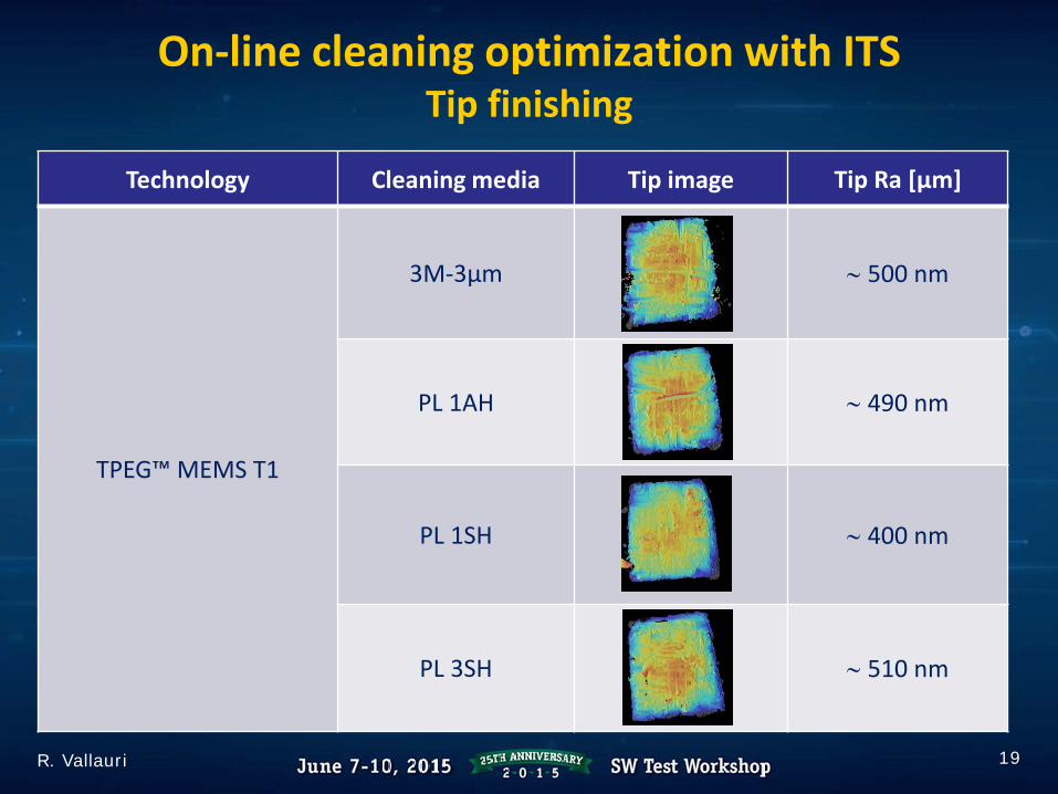
On-line cleaning optimization with ITSTip finishing
19R. Vallauri
Technology Cleaning media Tip image Tip Ra [µm]
TPEG™ MEMS T1
3M-3µm ∼ 500 nm
PL 1AH ∼ 490 nm
PL 1SH ∼ 400 nm
PL 3SH ∼ 510 nm
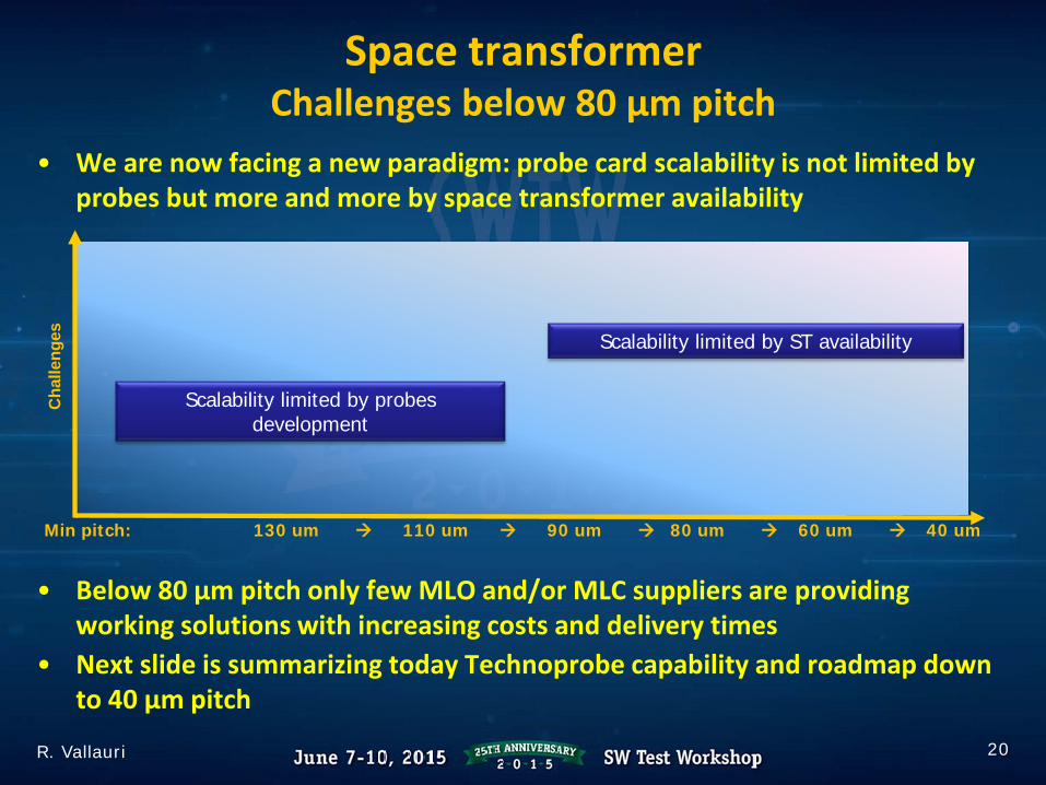
Space transformerChallenges below 80 µm pitch
20
• We are now facing a new paradigm: probe card scalability is not limited by probes but more and more by space transformer availability
• Below 80 µm pitch only few MLO and/or MLC suppliers are providing working solutions with increasing costs and delivery times
• Next slide is summarizing today Technoprobe capability and roadmap down to 40 µm pitch
Min pitch: 130 um 110 um 90 um 80 um 60 um 40 um
Cha
lleng
es Scalability limited by ST availability
Scalability limited by probes development
R. Vallauri
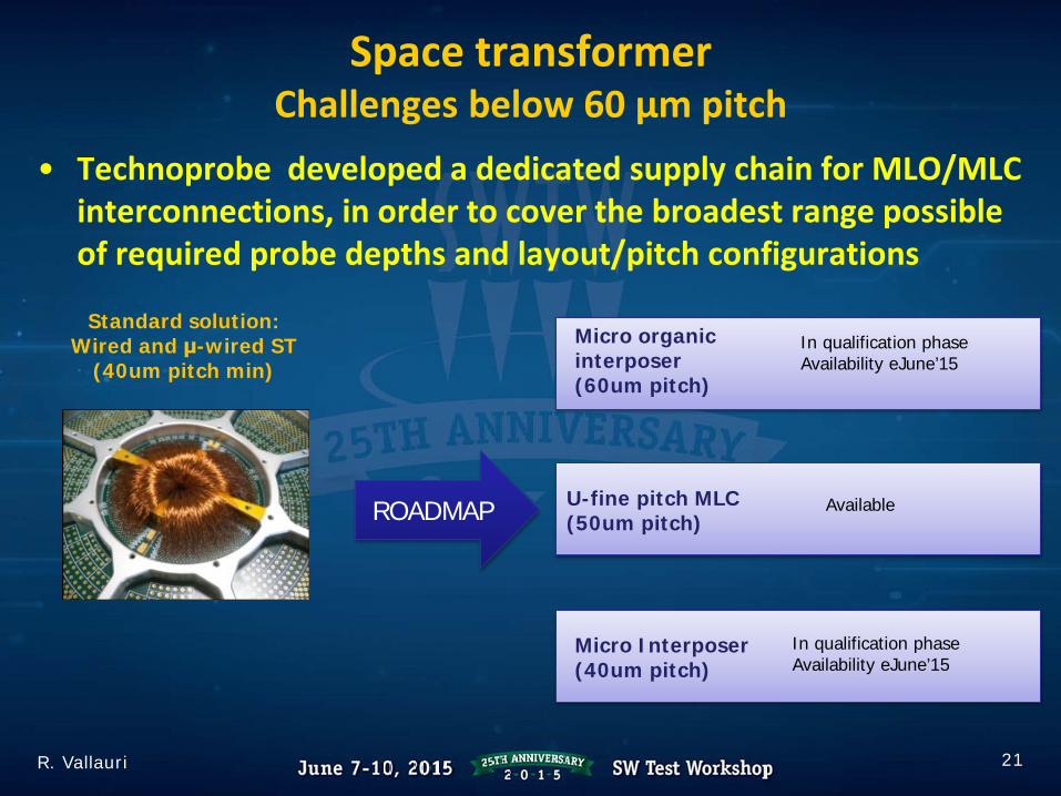
Space transformerChallenges below 60 µm pitch
21
• Technoprobe developed a dedicated supply chain for MLO/MLC interconnections, in order to cover the broadest range possible of required probe depths and layout/pitch configurations
Standard solution:Wired and μ-wired ST
(40um pitch min)
U-fine pitch MLC (50um pitch)
Micro Interposer (40um pitch)
Available
In qualification phaseAvailability eJune’15
ROADMAP
Micro organic interposer(60um pitch)
In qualification phaseAvailability eJune’15
R. Vallauri
22R. Vallauri
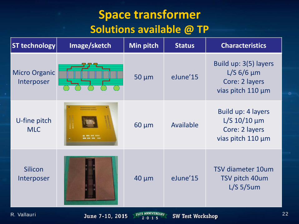
Space transformerSolutions available @ TP
ST technology Image/sketch Min pitch Status Characteristics
Micro Organic Interposer 50 µm eJune’15
Build up: 3(5) layers L/S 6/6 µm
Core: 2 layers vias pitch 110 µm
U-fine pitchMLC 60 µm Available
Build up: 4 layers L/S 10/10 µmCore: 2 layers
vias pitch 110 µm
SiliconInterposer 40 µm eJune’15
TSV diameter 10umTSV pitch 40um
L/S 5/5um
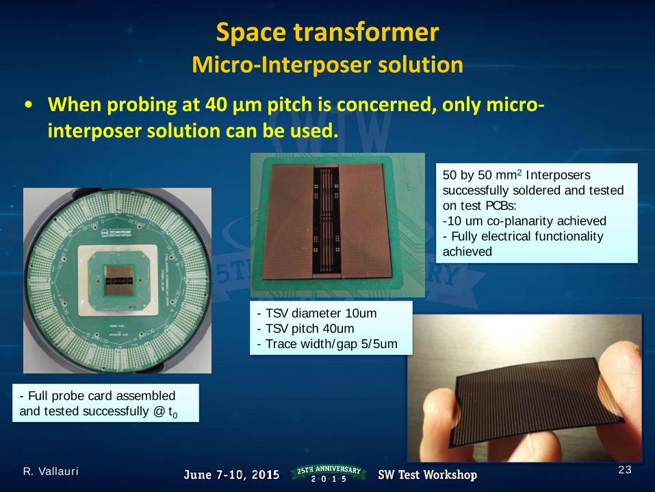
Space transformerMicro-Interposer solution
23
• When probing at 40 µm pitch is concerned, only micro-interposer solution can be used.
50 by 50 mm2 Interposers successfully soldered and tested on test PCBs:-10 um co-planarity achieved- Fully electrical functionality achieved
- Full probe card assembled and tested successfully @ t0
- TSV diameter 10um- TSV pitch 40um- Trace width/gap 5/5um
R. Vallauri
Conclusions
24
• We are in front of a two fold, huge change of probe card paradigms:– Probe cards moved from just an electro-mechanical interface to a system,
to be integrated in a high complexity probing environment– More recently probe card scalability is moving from probes/probe head
limitations to space transformer availability limitations
• Win/win strong partnerships are needed between main Suppliers and Customers to have full visibility of evolving requirements and full control of the design and manufacturing of most critical probe card components.
• The presentation gave you a quick overview of how Technoprobe is working to achieve this target
R. Vallauri
Future workOn-going developments down to 40 µm pitch
25
• Further developments are on-going to define the best possible probing solution to probe over µ-pads and µ-Cu pillars down to 40 µm pitch full array
• TPEG™ MEMS T40, recently introduced, will be tested within the cooperation frame between IMEC, Technoprobe and TEL
R. Vallauri
Thank you !
26
Raffaele VallauriR&D & Process Engineering Technoprobe Italy(+39) [email protected]
Daniele PeregoR&D EngineerTechnoprobe Italy(+39) [email protected]
Emanuele BertarelliR&D Technoprobe Italy(+39) [email protected]
Marco PreaMarketing MgrTechnoprobe Italy(+39) [email protected]
Erik-Jan MarinissenPrincipal Scientist 3D integration – Test & DFTIMEC Belgium(+32) 16 28-8755 [email protected]
Jerry BrozApplications Engineering Team LeaderInternational Test Solutions USA(+001) [email protected]