chapter 1
TRANSCRIPT

CHAPTER 1
INTRODUCTION
1.0. OVERVIEW OF THE PROJECT.
The Digital clock is the type of clock that displays time digitally. The digital clock was design in order to
enhance the student’s knowledge on circuit design using software’s, circuit building using bread board
and implementation of the circuit on PCB. This was made through contributions from all the group
members. Each and every member contributed to his best ability to ensure that the digital clock is being
created.
The digital clock has three mainly parts namely, the hour section, minute’s sections and the second’s
sections. Each of the minute and second section has been designed to give a count from 00 to 59 after
which it resets to 00 and the hour section to give a count from 00 to 23 hours after which it resets to 00.
For each cycle of 00 to 59 in second section the minute section increases its count by 1. Where all the
three sections will be generated from AT89C51 microcontroller which is from the 8051 family.
The Atmel AT89C51 is a powerful microcontroller which provides a highly-flexible and cost-effective
solution to many embedded control applications. The AT89C51 microcontroller is the one responsible in
generating the timing because it’s a programmable chip that has input and output pins, and also having
timer.
Finally all the three parts will be discussed later in the chapters.
1.1 AIM OF THE PROJECT
The main aim of this project is to build team work among the students and also to help the students to
enhance their knowledge and apply their knowledge to design and build a 24hrs digital clock.
1.2 OBJECTIVE OF THE PROJECT
1. To build a team working experience among students.
2. To design and build a digital clock
3. To develop a program for the microcontroller
1
1.3 PROJECT SPECIFICATIONS
The students were required to design a working 24hrs alarm digital clock. The students were given the
opportunity to use any method in creating the digital alarm or day indication clock which show’s hours,
minutes and seconds.
It was stated that the digital clock should have alarm or day indicator. Students were also required to
provide a power supply unit for the digital clock with a battery backup facility.
1.4 Module Structure
The entire project has been divided into Five modules. They are as follows:
Second section
Using port 1(Microcontroller) in such a way that this portion produces output from 00 to 59
continuously .
Using Driver IC (IC 7447) and seven-segment display to display the counts. Both the ICs are of
common anode type.
Checking the output of the circuit.
Minute section
Using port 2 (Microcontroller) in such a way that this portion produces output, the output should
count from 00 to 59 with a frequency of 1Hz.for
Using Driver IC (IC 7447) and seven-segment display to display the counts. Both the ICs are of
common anode type.
Checking the output of the circuit.
Hour section
Using port 0(Microcontroller) in such a way so that this portion produces output, the output should
counts from 23.59.59 then resets to 00.
Here the counting proceeds with a frequency of one pulse per hour.
Using Driver IC (IC 7447) and seven-segment display to display the counts. Both the ICs are of
common anode type.
Checking the output.
2

Day indication section
Port 3 is programmed in such a way to produce the day indications. When the time reaches 24hrs the
LED will light.
The 74138 IC will be used to switch on or off the LED when it reaches 24hrs.
Assembling the Four sections together.
Checking the final output of the circuit.
CHAPTER 23
LITERATURE REVIEW
2.1 Introduction
This chapter will present the overview about the digital clock.
2.2 Digital Clock Overview
Digital clock is a type of clock that displays the time digitally, as opposed to an analog clock,
where the time is displayed by hands. Digital clocks were invented in 1959 and became more popular as
microchips and LEDs became cheaply available. Digital clocks typically use the 50 or 60 hertz oscillation
of AC power or a crystal oscillator as in a quartz movement to keep time. To represent the time most
digital clocks use a seven segment LED or LCD.Usually, digital clocks are associated with electronic
drivers, unlike the analog clock which function is mechanically or also electrically driven. There are
many ways to design a digital clock such as using PIC, Atmel etc and C++, C or assembly languages are
used for the program. (http://www.waset.org/journals/waset/v42/v42-67.pdf)
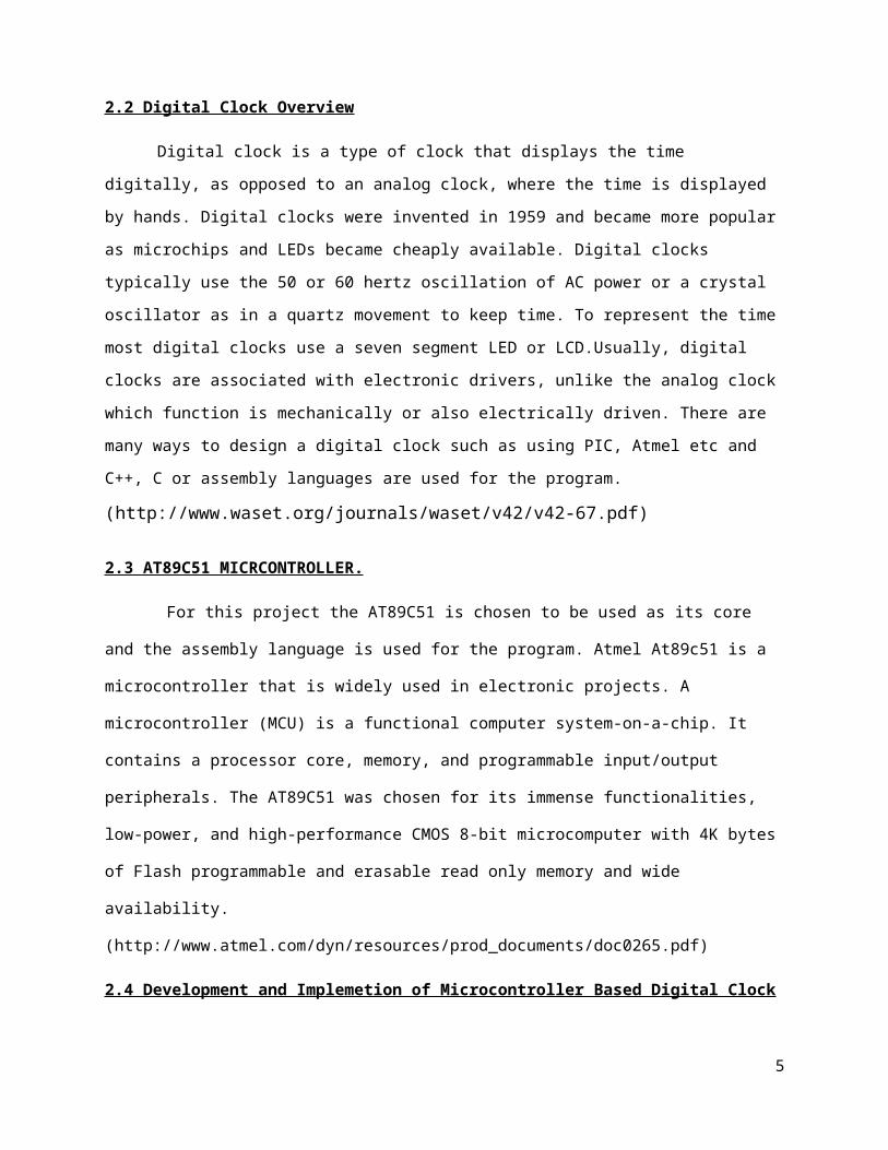
2.3 AT89C51 MICRCONTROLLER.
For this project the AT89C51 is chosen to be used as its core and the assembly language is used
for the program. Atmel At89c51 is a microcontroller that is widely used in electronic projects. A
microcontroller (MCU) is a functional computer system-on-a-chip. It contains a processor core, memory,
and programmable input/output peripherals. The AT89C51 was chosen for its immense functionalities,
low-power, and high-performance CMOS 8-bit microcomputer with 4K bytes of Flash programmable and
erasable read only memory and wide availability.
(http://www.atmel.com/dyn/resources/prod_documents/doc0265.pdf)
2.4 Development and Implemetion of Microcontroller Based Digital Clock
The digital electronic clocks have replaced the analog mechanical clock because they are much
reliable, accurate, maintenance free and portable. Mechanical analog clocks will need to be wound, and
their time keeping is not as accurate as quartz analog clocks or digital clocks. A digital clock is quite
accurate, and depending on the type it can also tell you the date, temperature and other information that an
analog clock simply cannot provide. (http://www.ehow.com/facts_7211103_analog-vs_-digital-clocks.html)
4
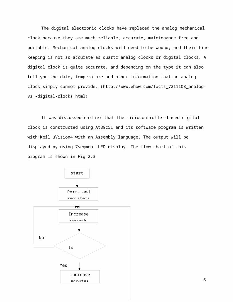
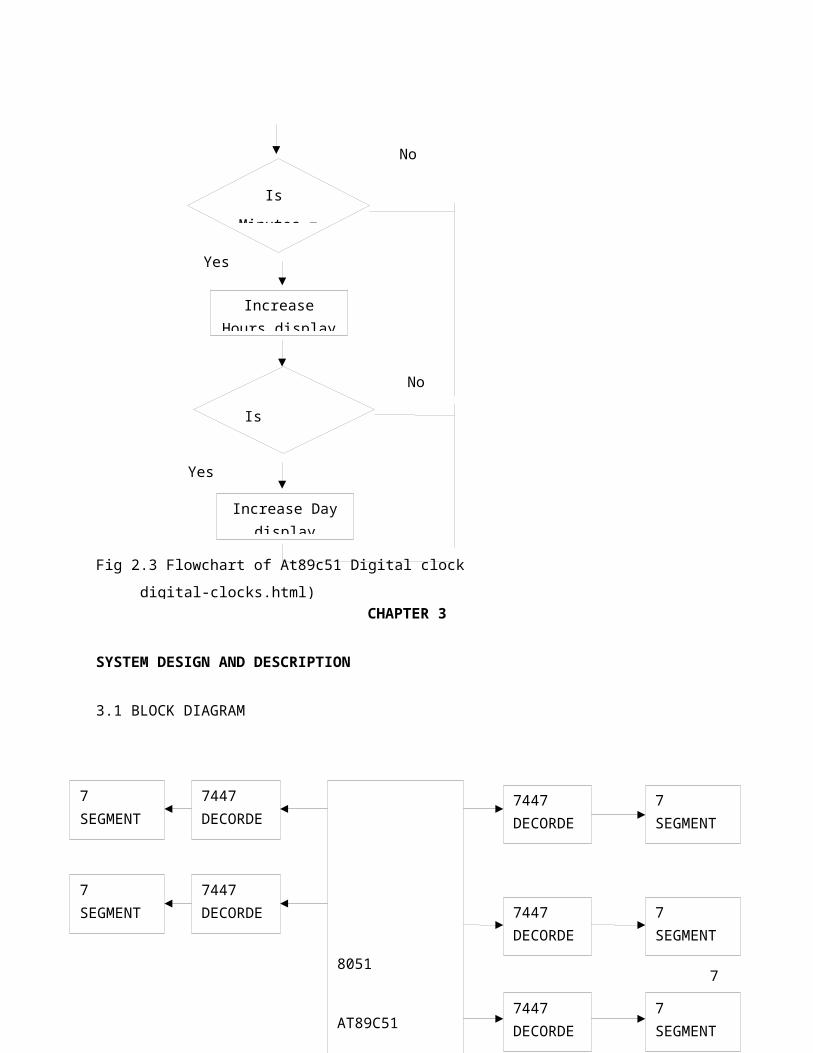
It was discussed earlier that the microcontroller-based digital clock is constructed using At89c51
and its software program is written with Keil uVision4 with an Assembly language. The output will be
displayed by using 7segment LED display. The flow chart of this program is shown in Fig 2.3
Fig 2.3 Flowchart of At89c51 Digital clock
5
start
Increase seconds display
Is
Seconds = 60
No
Ports and registers initialization
Yeso
Increase minutes display
Is
Minutes = 60
No
Increase Hours display
Yeso
Is
Hours=24
No
Yeso
Increase Day display
(http://www.ehow.com/facts_7211103_analog-vs_-digital-clocks.html)
CHAPTER 3
SYSTEM DESIGN AND DESCRIPTION
3.1 BLOCK DIAGRAM
3.2 POWER SUPPLY BLOCK DIGARAM
3.3 SYSTEM CIRCUIT DIAGRAM
6
PURE DC VOLTAGEAC VOLTAGE
8051
AT89C51
7447 DECORDER
7 SEGMENT
DISPLAY
7 SEGMENT
DISPLAY
7447 DECORDER
7447 DECORDER
7447 DECORDER
7447 DECORDER
7447 DECORDER
7 SEGMENT
DISPLAY
7 SEGMENT
DISPLAY
7 SEGMENT
DISPLAY
7 SEGMENT
DISPLAY
CRYSTAL
OSSILATOR
ALARM BUZZER
PUSH BUTTON
240 AC TRANSFORMER
BRIDGE RECTIFIER FILTER REGULATOR
HALF WAVE DC( impure) dc)
U1
8051
P1B0T21
P1B1T2EX2
P1B23
P1B34
P1B45
P1B5MOSI6
P1B6MISO7
P1B7SCK8
RST9
P3B0RXD10
P3B1TXD11
P3B4T014
P3B5T115
XTAL218
XTAL119
GND20 P2B0A8 21P2B1A9 22P2B2A10 23P2B3A11 24P2B4A12 25P2B5A13 26P2B6A14 27P2B7A15 28
P0B7AD7 32P0B6AD6 33P0B5AD5 34P0B4AD4 35P0B3AD3 36P0B2AD2 37P0B1AD1 38P0B0AD0 39VCC 40
P3B2INT012
P3B3INT113
P3B6WR16
P3B7RD17
PSEN 29ALEPROG 30EAVPP 31
U3
7447N
A 7B 1C 2D 6
OA13
OD10OE9OF15
OC11OB12
OG14~LT 3~RBI 5
~BI/RBO 4
U4
7447N
A 7B 1C 2D 6
OA13
OD10OE9OF15
OC11OB12
OG14~LT 3~RBI 5
~BI/RBO 4
U5
7447N
A7B1C2D6
OA 13
OD 10OE 9OF 15
OC 11OB 12
OG 14~LT3~RBI5~BI/RBO4
VCC5V
X1HC-49/U_11MHz
C3
33pF
C533pF C6
33pF
R210kΩ
J2
Key = Space
U8
7447N
A7B1C2D6
OA 13
OD 10OE 9OF 15
OC 11OB 12
OG 14~LT3~RBI5~BI/RBO4
U2
7447N
A7B1C2D6
OA 13
OD 10OE 9OF 15
OC 11OB 12
OG 14~LT3~RBI5~BI/RBO4
V1
230 Vrms 50 Hz 0°
U6LM7805CTLINE VREG
COMMON
VOLTAGEC11mF
T1D1
1B4B42 1
2
4
3
D21N4001
Battery9 V
U7
74LS138D
Y015Y114Y213Y312Y411Y510Y69Y77
A 1B 2C 3
G1 6~G2A 4~G2B 5
TUEmon
WEDTHU
FRISATSUN
U9
7447N
A7B1C2D6
OA 13
OD 10OE 9OF 15
OC 11OB 12
OG 14~LT3~RBI5~BI/RBO4
3.4 COMPONENTS USED
Material quantity
i. AT89C51 microcontroller 1ii. 7447 decoder 6
iii. 74138 decoder 1iv. LED 7v. Transformer 1
vi. Bridge rectifier 1vii. Electrolytic capacitor (1000uF) 1
viii. Regulator(LM7805) 1ix. Push button 1x. Diode 1
xi. 9V Battery
7

3.5 MICROCONTROLLER AT89C51
The AT89C51 is a low-power, high-performance CMOS 8-bit microcomputer with 4Kbytes of Flash
programmable and erasable read only memory. The Atmel AT89C51 is a powerful microcomputer which
provides a highly-flexible and cost-effective solution to many embedded control applications.
The device is manufactured using Atmel's high-density nonvolatile memory technology and is compatible
with the industry-standard 8051 instruction set and pin-out. The AT89C51 provides s, two 16-bit
timer/counters, on-chip oscillator, and clock circuitry
http://www.atmel.com/dyn/resources/prod_documents/doc0265.pdf
3.6 AT89C51 PIN DESCRIPTION
The Atmel AT89C51 used in this project is a 40 pin AT89C51. Where it
is divided into port 0, port 1, port 2, port 3, while the remaining pins
went to ground, Vcc, reset and crystal oscillator etc.
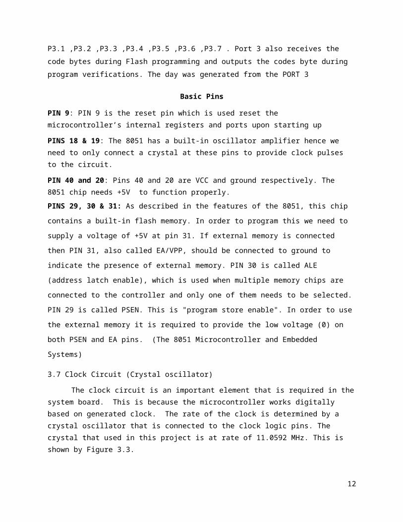
PORT 0 (pins 32 to 39)
The port zero is the first upper right side port of the microcontroller, which consists of 8 pins which are P1.0, P1.1 ,P2.2 ,P3.3 ,P4.4,P5.5 ,P6.6 ,P7.7 . Port 0 also receives the code bytes during Flash programming and outputs the codes byte during program verifications. The Hours’ section was generated from the PORT 0
PORT 1 Pins 1 to 8)
The port zero is the first upper left side port of the microcontroller, which consists of 8 pins which are P1.0, P1.1 ,P1.2 ,P1.3 ,P1.4 ,P1.5 ,P1.6 ,P1.7 . Port 1 also receives the code bytes during Flash programming and outputs the codes byte during program verifications. The second’s section was generated from the PORT 1
PORT 2 (pins 21 to 28)
8

The port zero is the second lower right side port of the microcontroller, which consists of 8 pins which
are P2.0, P2.1 ,P2.2 ,P2.3 ,P2.4 ,P2.5 ,P2.6 ,P2.7 . Port 2 also receives the code bytes during Flash
programming and outputs the codes byte during program verifications. The minutes section was
generated from the PORT 2
PORT 3 (Pins 10 to 17)
The port zero is the second lower left side port of the microcontroller, which consists of 8 pins which are
P3.0, P3.1 ,P3.2 ,P3.3 ,P3.4 ,P3.5 ,P3.6 ,P3.7 . Port 3 also receives the code bytes during Flash
programming and outputs the codes byte during program verifications. The day was generated from the
PORT 3
Basic Pins
PIN 9: PIN 9 is the reset pin which is used reset the microcontroller’s internal registers and ports upon
starting up
PINS 18 & 19: The 8051 has a built-in oscillator amplifier hence we need to only connect a crystal at
these pins to provide clock pulses to the circuit.
PIN 40 and 20: Pins 40 and 20 are VCC and ground respectively. The 8051 chip needs +5V to function
properly.
PINS 29, 30 & 31: As described in the features of the 8051, this chip contains a built-in flash memory. In
order to program this we need to supply a voltage of +5V at pin 31. If external memory is connected then
PIN 31, also called EA/VPP, should be connected to ground to indicate the presence of external memory.
PIN 30 is called ALE (address latch enable), which is used when multiple memory chips are connected to
the controller and only one of them needs to be selected. PIN 29 is called PSEN. This is "program store
enable". In order to use the external memory it is required to provide the low voltage (0) on both PSEN
and EA pins. (The 8051 Microcontroller and Embedded Systems)
3.7 Clock Circuit (Crystal oscillator)
The clock circuit is an important element that is required in the system board. This is because the
microcontroller works digitally based on generated clock. The rate of the clock is determined by a crystal
oscillator that is connected to the clock logic pins. The crystal that used in this project is at rate of
11.0592 MHz. This is shown by Figure 3.3.
X1HC-49/U_11MHz
C3
33pF
C6
33pF
9
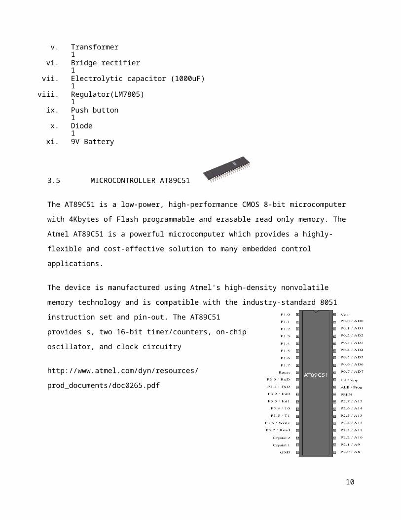
Figure 3.3
3.8 7 SEGMENT LED DISPLAY.
A seven-segment display, is a form of electronic display device for displaying decimal numerals that are
widely used in digital clocks and electronic meters etc. The seven segment display is the most basic
electronic display device that can display digits from 0-9.The seven-segment display is divided into two
kinds namely:- common anode and common cathode. But in this project the common anode seven-
segment display was used because 7447 is used as the decoder.
PIN DISCRIPTION
In a common anode display, the anodes of all the LEDs are joined together and the individual segments
are illuminated by connecting to a low voltage. The common anode seven- segment is having a-g outputs,
Vcc pin and dp pin. The a-g outputs are connected to the 7447 decoder respectively. And the Vcc pin is
connected to the 5 Voltage supply, while the dp is connected to ground. The diagram below shows a
common anode 7 segment display. (http://www.thelearningpit.com/lp/doc/7seg/7seg.htm)
http://www.thelearningpit.com/lp/doc/7seg/7seg.html
3.9.74LS139 DECODER/ DEMULTIPLEXER
The 74LS139 is a 16 pin decoder that is designed to be used in high-performance memory-decoding or
data-routing applications, requiring very short propagation delay times. It is used in the digital clock on
the day indication to be switching ON one LED and switching OFF the remaining 6 LED’s when the time
reaches 24hrs, as the day LED will automatically change.
3.10.PIN DESCRIPTION
10

The 74138 is having a total of 16 pins. Where the inputs are all connected the port 3 of microcontroller
and the outputs to each LED.
(http://focus.ti.com/lit/ds/symlink/sn74ls138.pdf)Connection Procedure.
1. Pin 16, pin 6 are connected to 5volts supply and pin 4, pin 5and pin 8 to ground.
2. Pins 13, 12, 11, 10, 9, 15 and 14 of the 74138, are connected to the cathode of the 7 LED’s.
3. Connect the pins1 , pin 2 and pin 3 to the port 3( P3.0,P3.1,P3.2) of the microcontroller.
3.11 7447 DECORDER
The 7447 decoder is used in displaying the time as numbers because the microcontroller accepts and
provides data’s in binary or hexadecimal form , so then the 7447 is used in displaying time as numerical.
The 7447 decoder IC is a 16 pin IC from the 74LS family. Which is designed for driving common anode
LED or 7 segment LED displays. The display is only sensible if the binary number is between
DCBA=0000 (0) and DCBA=1001 (9); this is called Binary Coded Decimal or BCD for short. If the
number is larger than 9 you get a strange output on the display. The 7447 only drives a common anode
seven- segment. (http://focus.ti.com/lit/ds/symlink/sn74ls47.pdf
3.12 7447 PIN DESCRIPTION
The 7447 is having a total of 16 pins. Where the inputs are all connected the port 0,port1 and port 2 of
microcontroller.
http://focus.ti.com/lit/ds/symlink/sn74ls47.pdf
11
Connection Procedure
1. Connect 330-ohm resistors to Pin 16 to 5volts supply and pin 8 to ground.2. Connect pins 13, 12, 11, 10, 9, 15 and 14 of the 7447, to the, b, c, d, e, f, and g segments of the 7-
segment LED.3. Connect the pins 1,2,6 and pin 7 of the 7447 to the A,B,C,D of the microcontroller.
BCD INPUT OUTPUT ( 7segment) DISPLAY
D C B A a b c d e f g
0 0 0 0 1 1 1 1 1 1 0 0
0` 0 0 1 0 1 1 0 0 0 0 1
0 0 1 0 1 1 0 1 1 0 1 2
0 0 1 1 1 1 1 1 0 0 1 3
0 1 0 0 0 1 1 0 0 1 1 4
0 1 0 1 1 0 1 1 0 1 1 5
0 1 1 0 0 0 1 1 1 1 1 6
0 1 1 1 1 1 1 0 0 0 0 7
1 0 0 0 1 1 1 1 1 1 1 8
1 0 0 1 1 1 1 0 0 1 1 9
TRUTH TABLE
CHAPTER 4
4.1 SOFTWARE IMPLEMETATION
i. Description of codings:-
The hour, minutes, seconds and the day indication section were obtained or generated from the
AT89C51 microcontroller through series of codes. The four sections codes will be explained below:
12

Seconds section
First initialize the data value to the port 1 by moving 00 hexadecimal to register 0, then move the register 0
to port 1 of the microcontroller because the digital clock starts at 0 seconds. Acall delay is a function used
as a time delay for setting the clock frequency. The whole program starts from increasing the second by one
using the accumulator (A) and the seconds is converted from hexadecimal to decimal using DA, which
mean decimal adjustment, then move A back to register 0 then to port 1 It will then compare the value at the
register 0 with 60 hexadecimal; if it is not equal 60, it will jump back to the start and add one to the second.
After the second is equal to 60, it will reset the value of the R0 to 00 and start increasing the minute by one.
Note:-
- DA A means decimal adjustment for addition, which converts hexadecimal to decimal values. The
DA instruction works only on A. In other word, while the source can be an operand of any
addressing mode, the destination must be in register A in order for DA to work.
- The A is a register called the accumulator, and by default it receives the result of all arithmetic
operations.
- R0 is a register in port 1 used to store information temporarily.
PSEUDOCODES IMPLEMENTATION
SECONDS
Move data 00 to register0
Move register0 to port1
Label START
13

Move register0 to port1
Move register0 to Accumulator A
Call DELAY
Add 1 to Accumulator
Decimal adjustment Accumulator
Move Accumulator to register0
Move register1 to port1
Compare register0 with 60
If register0 not equal to 60
Go to START
If register0 equal 60
Move data 00 to register0
DELAY
Move data 10 to register7
Label L3
Move data 200 to register6
Label L2
Move data 250 to register5
Label L1
Compare register5 with 0
If register5 not equal to 0
Decrease register5 by 1 and go to L1
If register5 equal to 0
Compare register6 with 0
If register6 not equal to 0
14

Decrease register6 by 1 and go to L2
If register6 equal to 0
Compare register7 with 0
If register7 not equal to 0
Decrease register7 by 1 and go to L3
If register7 equal to 0
Return to program after delay.
Minutes section:
First initialize the data value to the port 2 by moving 00 hexadecimal to register 2, then move the register 2
to port 2 of the microcontroller because the digital clock starts at 0 minutes. The whole program starts from
increasing the minutes by one using the accumulator (A) and the minutes is converted from hexadecimal to
decimal using DA, which mean decimal adjustment, then move A back to register 2 then to port 2. It will
then compare the value at the register 2 with 60 hexadecimal; if it is not equal 60 it will jump all the way
back to the increment of seconds till the seconds reaches 60 seconds before adding one to the minutes. After
the minute is equal to 60, it will reset the value of the R2 to 00 and start increasing the hour by one.
MINUTES PSEUDOCODES
Move data 00 to register2
Move register2 to port2
Move register2 to Accumulator A
Add 1 to Accumulator
Decimal adjustment Accumulator
Move Accumulator to register2
Move register2 to port2
Compare register2 with 60
If register2 not equal to 60
Go to START
15

If register2 equal 60
Move data 00 to register2
Move register2 to port2
Hour section:-
Once the minute reach 60, it will reset the value of Register2 to 00 and start increasing the hour by one.
Port0 is used for the hour display. After adding one to Register1, the program will compare Register1
with 24, if it is not equal; it will jump back to seconds counting till it reaches 60 seconds and go all the
way to 60 minutes again before adding one to the hour. When the hour reaches 24, it will be reset to 00
and the whole digital clock will reset to 0, which is the initial condition. And then repeat the entire three
processes continuously, That was why SJMP was used.
Note:-
- SJMP mean short jump, which is used in repeating the seconds, minutes and hours continuously.
HOURS PSEUDOCODES
Move register1 to Accumulator A
Add 1 to Accumulator
Decimal adjustment Accumulator
Move Accumulator to register1
Compare register1 with 24
If register1 not equal to 24
Go to START
If register1 equal 24
Move data 00 to register1
Move register1 to port1
Day indication section:-
Port 3 of the microcontroller is used for day indicator. First, declare register 3 as 0 and move it to port 3. This will be the initial condition, which is the first day when the digital clock starts. This data is then comparing with 7, if it is not equal; it will continue showing 0 until the next 24 hours
16

reached. The port 3 of microcontroller is connected with a demultiplexer 74138, which will convert the data to binary and light the respective LED.
After 24 hours, the value of register 3 will be increased by 1 and compare again with 7. The whole process will continue until the value reaches 7, where it will be reset to 0 again after 24 hours.
DAY INDICATOR PSEUDOCODES
Increase register3
Compare register3 with 7
If register3 not equal to 7
Go to SKIP
If register3 equal to 7
Move data 00 to register3
Label SKIP
Move register3 to port3
4.2.HARDWARE CONSTRUCTION
The entire digital clock was first build on a breadboard to test the connections, and later on the
components were placed on a Printed circuited board. The printed circuit processes will be explained
below:
P.C.B. DESIGNING
i. P.C.B. LAYOUT
The entire circuit was assembled on a general purpose PCB board. PCB layout of the circuit and
preparations are the first and most important in any printed circuit board. Firstly layouts of components
were designed according to the available component dimensions in a PCB software.
The following points are to be observed while forming a PCB:
1. Between two components, sufficient space should be maintained to avoid partial contacts
2. High voltage dissipated components should be mounted at a sufficient distance from
semiconductor and electrolytic capacitors.
17
P.C.B. DESIGNING & WORKING

Printed circuit board (P.B.C) is used to avoid most of all the disadvantages of convectional breadboard.
These also avoid the use of thin wires for connecting the components.
PCB consist of the following processes:-
1. Designing in the software
2. Ironing
3. Etching
4. Drilling
5. Soldering
6. Troubleshooting.
4.3 ELECTRICAL CONSTRUCTION.
The entire clock was controlled electrically with the use of the power supply unit. Where the power supply unit consists of different components as shown in Fig 4.3 :-
V1
230 Vrms 50 Hz 0°
U6LM7805CTLINE VREG
COMMON
VOLTAGEC11mF
T1D1
1B4B42 1
2
4
3
D21N4001
Battery9 V
Fig 4.3
1. Transformer:-To step down high voltage AC mains to low voltage AC.
2. Bridge Rectifier:- To convert AC to DC, but the DC output is varying.
3. Electrolytic capacitor:- To smooth the DC from varying greatly to a small ripple.
4. 7805:- To eliminate ripple by setting DC output to a 5 voltage.
5. 1N4001: To serve as switch between main supply and the battery.
6. Battery: To serve as backup power supply.
CHAPTER 5
RESULTS AND DISCUSSION.
5.1. SIMULATION RESULTS AND DISCUSSION 18

In this chapter, the power supply unit will be discussed in detail.
1. Transformer:- To step down high voltage AC to low voltage AC.The output result is shown below:
Input signal output signal
2. Bridge Rectifier:- To convert AC to DC, but the DC output is varying. The output is shown below:
V1
230 Vrms 50 Hz 0°
D1
1B4B42
1
2
4
3
T1
XSC1
A B
Ext Trig+
+
_
_ + _
3. Filter:- smooth the DC from varying greatly to a small ripple. The output result is shown below:
T1C21mF
V1
230 Vrms 50 Hz 0°
D1
1B4B42
1
2
4
3
XSC1
A B
Ext Trig+
+
_
_ + _
4. Regulator:- To eliminate ripple by setting DC output to a 5 voltage. The output result is shown below:
19
V1
230 Vrms 50 Hz 0°
D1
1B4B42
1
2
4
3
T1C11mF
U1LM7805CTLINE VREG
COMMON
VOLTAGE
XSC1
A B
Ext Trig+
+
_
_ + _
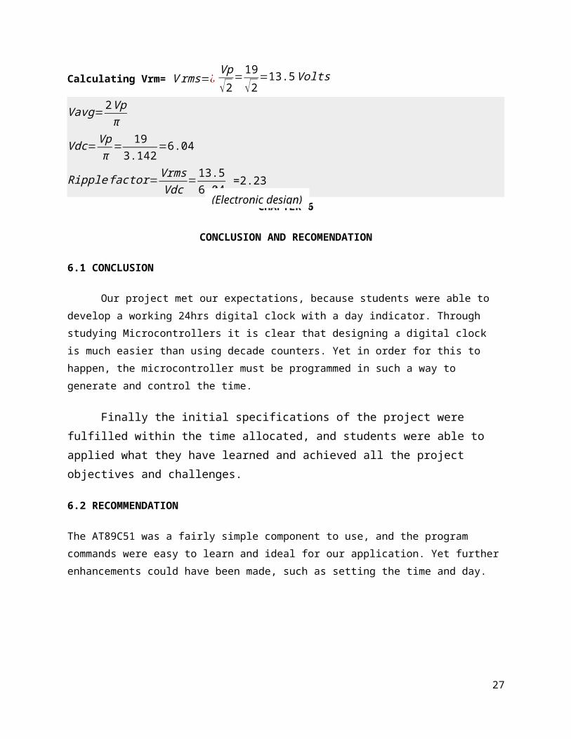
5.2 DESIGN CALCULATIONS
Calculating 330 ohms resistor for 7 segment
7 segment voltage=1.7volts
7 segment current=10mA
Total voltage=5Volts
R= 5 v−1.7 v
10 mA=330ohms
Calculating electrolytic capacitor.
c= Vsmax∆ V . Fp. RL
c= 25(25−7 )∗50 Hz∗29
=957.85uF ≅ 1000 uF
Calculating the period , T= 1F
= 150 Hz
=20 mS
Calculating Vpp = Vpp=Vmax−Vmin=19.2 — (−18.8)
Vpp=38.0 Volts
Vp=Vpp2
=382
=19 V
Calculating Vrm= V rms=¿ Vp
√2=19
√2=13.5Volts
Vavg=2 Vpπ
20
Where :−Vsmax of regulator=25 volts
Vmin of regulator=7 volts ,
∆ V ¿ ¿ the regulator ¿=25 V−7 V
Fp=50 Hz
RL=29 Ώ
Vdc=Vpπ
= 193.142
=6.04
Ripple factor=VrmsVdc
=13.56.04
=2.23
CHAPTER 6
CONCLUSION AND RECOMENDATION
6.1 CONCLUSION
Our project met our expectations, because students were able to develop a working 24hrs digital
clock with a day indicator. Through studying Microcontrollers it is clear that designing a digital clock is
much easier than using decade counters. Yet in order for this to happen, the microcontroller must be
programmed in such a way to generate and control the time.
Finally the initial specifications of the project were fulfilled within the time allocated, and
students were able to applied what they have learned and achieved all the project objectives and
challenges.
6.2 RECOMMENDATION
The AT89C51 was a fairly simple component to use, and the program commands were easy to learn and
ideal for our application. Yet further enhancements could have been made, such as setting the time and
day.
21
(Electronic design)
REFERENCE:-
Online:
At89c51 datasheet available at http://www.keil.com/dd/docs/datashts/atmel/at89c51_ds.pdf
accessed march 6th 2011
http://en.wikibooks.org/wiki/Embedded_Systems/8051_Microcontroller accessed March 10th
2011
JOHN HEWES power supply unit 2010 available at http://www.kpsec.freeuk.com/powersup.htm,
accessed april 1st 2011.
PERRY ANDREWS Digital Clock September 2007 available at
http://www.pelnet.co.uk/elect/projects/clock/Clock_a.pdf accessed April 2nd 2011
NOOR AZIANA Real time clock display MAY 2006 available at
http://library.utem.edu.my/index2.php?
option=com_docman&task=doc_view&gid=691&Itemid=113 accessed April 2nd 2011
74LS47 datasheet available at http://focus.ti.com/lit/ds/symlink/sn74ls47.pdf accessed on 4th April
2011
74LS138 datasheet available at http://focus.ti.com/lit/ds/symlink/sn74ls138.pdf accessed 6th
April 2011
Interfacing to7-Segment Numeric Displays available at
http://www.thelearningpit.com/lp/doc/7seg/7seg.htm accessed march 10
7447 BCD to 7-segment display driver available at http://www.elektropage.com/default.asp?
tid=438&kw=Drives accessed march 2nd 2011
Elaine Anderson Analog Vs. Digital Clocks 2010 available at
(http://www.ehow.com/facts_7211103_analog-vs_-digital-clocks.html) accessed march 12th 2011
Pan Thu Tun Development and Implementation of Microcontroller-based Digital Clock
2008available at (http://www.waset.org/journals/waset/v42/v42-67.pdf) accessed 20th march 2011
BOOKS:-
1. Muhammad Ali Mazidi, Janice Gillispie Mazidi, Rolin D. McKinlay The8051 Microcontroller
and Embedded Systems Using Assembly and C Second Edition Prentice Hall Inc.
22
2. Savant, Roben, Carpenter Electronic design second edition 1991 Addison-wesley .
APPENDIX
Coding using assembly language
ORG 00 // Start for the program
MOV R3,#00H
MOV P3,R3
LOOP: MOV R0,#00H
MOV P0, R0
MOV R1,#00H
MOV P1,R1
MOV R2,#00H
MOV P2,R2
START: MOV P0, R0
MOV A, R0
ACALL DELAY
ADD A,#1
DA A
MOV R0,A
MOV P1,R1
SKIP1: CJNE R0,#60H,START
MOV R0,#00H
MOV A,R2
ADD A,#1
DA A
MOV R2,A
23

MOV P2,R2
CJNE R2,#60H,START
MOV R2,#00H
MOV P2,R2
MOV A,R1
ADD A,#1
DA A
MOV R1,A
CJNE R1, #24H, START
MOV R1,#00H
MOV P1,R1
INC R3
CJNE R3,#7H,SKIP
MOV R3,#00H
SKIP: MOV P3,R3
SJMP LOOP
DELAY: MOV R7,#10
L3: MOV R6,#200
L2: MOV R5,#250
L1: DJNZ R5,L1
DJNZ R6,L2
DJNZ R7,L3
RET
END
PCB LAYOUT
Seven segment
24

Complete system with power supply unit.
Power supply unit from a digital oscilloscope
Main digital clock on PCB board
25

PCB processes
26
7447 and 7 a segment on breadboard System on breadboard
Cost Analysis of components used
27

28
PROJECT SCHEDULE
ACTIVITIES DURATION
(WEEKS)
JANUARY FEBUARY MARCH APRIL
- - 1 2 3 4 5 6 7 8 9 10 11 12
1. TITLE SELECTION 1
2. LITERATURE RESEARCH
2
3. PROJECT PLANNING 1
4. CIRCUIT DESIGN 4
5. HARDWARE DESIGN 3
6. SOFTWARE DEVELOPMENT
2
7. PROJECT TESTING 1
8. FINAL REPORT PREPARATION AND SUBMISSION
2
9. PROJECT DEMONSTRATION
1
10. PROJECT PRESENTATION PREPARATION
1